JP4914119B2 - Plasma processing method and plasma processing apparatus - Google Patents
Plasma processing method and plasma processing apparatus Download PDFInfo
- Publication number
- JP4914119B2 JP4914119B2 JP2006152305A JP2006152305A JP4914119B2 JP 4914119 B2 JP4914119 B2 JP 4914119B2 JP 2006152305 A JP2006152305 A JP 2006152305A JP 2006152305 A JP2006152305 A JP 2006152305A JP 4914119 B2 JP4914119 B2 JP 4914119B2
- Authority
- JP
- Japan
- Prior art keywords
- discharge
- break
- plasma processing
- plasma
- determining
- Prior art date
- Legal status (The legal status is an assumption and is not a legal conclusion. Google has not performed a legal analysis and makes no representation as to the accuracy of the status listed.)
- Expired - Fee Related
Links
- 238000012545 processing Methods 0.000 title claims description 171
- 238000003672 processing method Methods 0.000 title claims description 4
- 239000007789 gas Substances 0.000 claims description 40
- 230000007423 decrease Effects 0.000 claims description 23
- 239000003990 capacitor Substances 0.000 claims description 19
- 229910052799 carbon Inorganic materials 0.000 claims description 9
- OKTJSMMVPCPJKN-UHFFFAOYSA-N Carbon Chemical compound [C] OKTJSMMVPCPJKN-UHFFFAOYSA-N 0.000 claims description 8
- 229910052739 hydrogen Inorganic materials 0.000 claims description 5
- 239000001257 hydrogen Substances 0.000 claims description 5
- 125000004435 hydrogen atom Chemical class [H]* 0.000 claims 2
- 238000005530 etching Methods 0.000 description 43
- 238000004140 cleaning Methods 0.000 description 38
- 235000012431 wafers Nutrition 0.000 description 35
- 238000000034 method Methods 0.000 description 21
- 238000010586 diagram Methods 0.000 description 16
- 238000001179 sorption measurement Methods 0.000 description 16
- 230000007704 transition Effects 0.000 description 15
- 239000007795 chemical reaction product Substances 0.000 description 9
- 238000012546 transfer Methods 0.000 description 8
- 238000004519 manufacturing process Methods 0.000 description 7
- 238000001020 plasma etching Methods 0.000 description 7
- PXGOKWXKJXAPGV-UHFFFAOYSA-N Fluorine Chemical compound FF PXGOKWXKJXAPGV-UHFFFAOYSA-N 0.000 description 6
- 229910052731 fluorine Inorganic materials 0.000 description 6
- 239000011737 fluorine Substances 0.000 description 6
- 239000004065 semiconductor Substances 0.000 description 6
- 230000008859 change Effects 0.000 description 5
- 229910021420 polycrystalline silicon Inorganic materials 0.000 description 4
- 229920005591 polysilicon Polymers 0.000 description 4
- 230000001186 cumulative effect Effects 0.000 description 3
- 150000002431 hydrogen Chemical class 0.000 description 3
- 238000012544 monitoring process Methods 0.000 description 3
- 230000008569 process Effects 0.000 description 3
- 238000013480 data collection Methods 0.000 description 2
- 230000004069 differentiation Effects 0.000 description 2
- 230000003993 interaction Effects 0.000 description 2
- 230000007246 mechanism Effects 0.000 description 2
- 239000013307 optical fiber Substances 0.000 description 2
- 239000000126 substance Substances 0.000 description 2
- 239000000758 substrate Substances 0.000 description 2
- HSFWRNGVRCDJHI-UHFFFAOYSA-N Acetylene Chemical compound C#C HSFWRNGVRCDJHI-UHFFFAOYSA-N 0.000 description 1
- LFQSCWFLJHTTHZ-UHFFFAOYSA-N Ethanol Chemical compound CCO LFQSCWFLJHTTHZ-UHFFFAOYSA-N 0.000 description 1
- 230000009471 action Effects 0.000 description 1
- 238000001514 detection method Methods 0.000 description 1
- 238000007599 discharging Methods 0.000 description 1
- 238000009826 distribution Methods 0.000 description 1
- 230000005684 electric field Effects 0.000 description 1
- 238000002474 experimental method Methods 0.000 description 1
- 235000011194 food seasoning agent Nutrition 0.000 description 1
- 229910052736 halogen Inorganic materials 0.000 description 1
- 150000002367 halogens Chemical class 0.000 description 1
- 239000000463 material Substances 0.000 description 1
- 238000010606 normalization Methods 0.000 description 1
- 230000002093 peripheral effect Effects 0.000 description 1
- 238000000513 principal component analysis Methods 0.000 description 1
- 239000000047 product Substances 0.000 description 1
- 238000001228 spectrum Methods 0.000 description 1
- 230000000087 stabilizing effect Effects 0.000 description 1
- XLYOFNOQVPJJNP-UHFFFAOYSA-N water Substances O XLYOFNOQVPJJNP-UHFFFAOYSA-N 0.000 description 1
Images


Classifications
-
- H—ELECTRICITY
- H01—ELECTRIC ELEMENTS
- H01J—ELECTRIC DISCHARGE TUBES OR DISCHARGE LAMPS
- H01J37/00—Discharge tubes with provision for introducing objects or material to be exposed to the discharge, e.g. for the purpose of examination or processing thereof
- H01J37/32—Gas-filled discharge tubes
- H01J37/32917—Plasma diagnostics
- H01J37/32935—Monitoring and controlling tubes by information coming from the object and/or discharge
- H01J37/32963—End-point detection
-
- H—ELECTRICITY
- H01—ELECTRIC ELEMENTS
- H01L—SEMICONDUCTOR DEVICES NOT COVERED BY CLASS H10
- H01L21/00—Processes or apparatus adapted for the manufacture or treatment of semiconductor or solid state devices or of parts thereof
- H01L21/02—Manufacture or treatment of semiconductor devices or of parts thereof
- H01L21/04—Manufacture or treatment of semiconductor devices or of parts thereof the devices having potential barriers, e.g. a PN junction, depletion layer or carrier concentration layer
- H01L21/18—Manufacture or treatment of semiconductor devices or of parts thereof the devices having potential barriers, e.g. a PN junction, depletion layer or carrier concentration layer the devices having semiconductor bodies comprising elements of Group IV of the Periodic Table or AIIIBV compounds with or without impurities, e.g. doping materials
- H01L21/30—Treatment of semiconductor bodies using processes or apparatus not provided for in groups H01L21/20 - H01L21/26
- H01L21/302—Treatment of semiconductor bodies using processes or apparatus not provided for in groups H01L21/20 - H01L21/26 to change their surface-physical characteristics or shape, e.g. etching, polishing, cutting
- H01L21/306—Chemical or electrical treatment, e.g. electrolytic etching
- H01L21/3065—Plasma etching; Reactive-ion etching
-
- H—ELECTRICITY
- H01—ELECTRIC ELEMENTS
- H01J—ELECTRIC DISCHARGE TUBES OR DISCHARGE LAMPS
- H01J37/00—Discharge tubes with provision for introducing objects or material to be exposed to the discharge, e.g. for the purpose of examination or processing thereof
- H01J37/32—Gas-filled discharge tubes
- H01J37/32009—Arrangements for generation of plasma specially adapted for examination or treatment of objects, e.g. plasma sources
- H01J37/32082—Radio frequency generated discharge
- H01J37/32091—Radio frequency generated discharge the radio frequency energy being capacitively coupled to the plasma
-
- H—ELECTRICITY
- H01—ELECTRIC ELEMENTS
- H01J—ELECTRIC DISCHARGE TUBES OR DISCHARGE LAMPS
- H01J37/00—Discharge tubes with provision for introducing objects or material to be exposed to the discharge, e.g. for the purpose of examination or processing thereof
- H01J37/32—Gas-filled discharge tubes
- H01J37/32009—Arrangements for generation of plasma specially adapted for examination or treatment of objects, e.g. plasma sources
- H01J37/32082—Radio frequency generated discharge
- H01J37/321—Radio frequency generated discharge the radio frequency energy being inductively coupled to the plasma
-
- H—ELECTRICITY
- H01—ELECTRIC ELEMENTS
- H01J—ELECTRIC DISCHARGE TUBES OR DISCHARGE LAMPS
- H01J37/00—Discharge tubes with provision for introducing objects or material to be exposed to the discharge, e.g. for the purpose of examination or processing thereof
- H01J37/32—Gas-filled discharge tubes
- H01J37/32009—Arrangements for generation of plasma specially adapted for examination or treatment of objects, e.g. plasma sources
- H01J37/32192—Microwave generated discharge
-
- H—ELECTRICITY
- H01—ELECTRIC ELEMENTS
- H01J—ELECTRIC DISCHARGE TUBES OR DISCHARGE LAMPS
- H01J37/00—Discharge tubes with provision for introducing objects or material to be exposed to the discharge, e.g. for the purpose of examination or processing thereof
- H01J37/32—Gas-filled discharge tubes
- H01J37/32917—Plasma diagnostics
- H01J37/32926—Software, data control or modelling
-
- H—ELECTRICITY
- H01—ELECTRIC ELEMENTS
- H01J—ELECTRIC DISCHARGE TUBES OR DISCHARGE LAMPS
- H01J37/00—Discharge tubes with provision for introducing objects or material to be exposed to the discharge, e.g. for the purpose of examination or processing thereof
- H01J37/32—Gas-filled discharge tubes
- H01J37/32917—Plasma diagnostics
- H01J37/32935—Monitoring and controlling tubes by information coming from the object and/or discharge
- H01J37/32981—Gas analysis
-
- H—ELECTRICITY
- H01—ELECTRIC ELEMENTS
- H01J—ELECTRIC DISCHARGE TUBES OR DISCHARGE LAMPS
- H01J37/00—Discharge tubes with provision for introducing objects or material to be exposed to the discharge, e.g. for the purpose of examination or processing thereof
- H01J37/32—Gas-filled discharge tubes
- H01J37/32917—Plasma diagnostics
- H01J37/3299—Feedback systems
-
- H—ELECTRICITY
- H01—ELECTRIC ELEMENTS
- H01L—SEMICONDUCTOR DEVICES NOT COVERED BY CLASS H10
- H01L21/00—Processes or apparatus adapted for the manufacture or treatment of semiconductor or solid state devices or of parts thereof
- H01L21/67—Apparatus specially adapted for handling semiconductor or electric solid state devices during manufacture or treatment thereof; Apparatus specially adapted for handling wafers during manufacture or treatment of semiconductor or electric solid state devices or components ; Apparatus not specifically provided for elsewhere
- H01L21/67005—Apparatus not specifically provided for elsewhere
- H01L21/67242—Apparatus for monitoring, sorting or marking
-
- H—ELECTRICITY
- H05—ELECTRIC TECHNIQUES NOT OTHERWISE PROVIDED FOR
- H05H—PLASMA TECHNIQUE; PRODUCTION OF ACCELERATED ELECTRICALLY-CHARGED PARTICLES OR OF NEUTRONS; PRODUCTION OR ACCELERATION OF NEUTRAL MOLECULAR OR ATOMIC BEAMS
- H05H1/00—Generating plasma; Handling plasma
- H05H1/24—Generating plasma
- H05H1/46—Generating plasma using applied electromagnetic fields, e.g. high frequency or microwave energy
-
- H—ELECTRICITY
- H01—ELECTRIC ELEMENTS
- H01J—ELECTRIC DISCHARGE TUBES OR DISCHARGE LAMPS
- H01J2237/00—Discharge tubes exposing object to beam, e.g. for analysis treatment, etching, imaging
- H01J2237/18—Vacuum control means
- H01J2237/182—Obtaining or maintaining desired pressure
- H01J2237/1825—Evacuating means
-
- H—ELECTRICITY
- H01—ELECTRIC ELEMENTS
- H01J—ELECTRIC DISCHARGE TUBES OR DISCHARGE LAMPS
- H01J2237/00—Discharge tubes exposing object to beam, e.g. for analysis treatment, etching, imaging
- H01J2237/32—Processing objects by plasma generation
- H01J2237/327—Arrangements for generating the plasma
-
- H—ELECTRICITY
- H01—ELECTRIC ELEMENTS
- H01J—ELECTRIC DISCHARGE TUBES OR DISCHARGE LAMPS
- H01J37/00—Discharge tubes with provision for introducing objects or material to be exposed to the discharge, e.g. for the purpose of examination or processing thereof
- H01J37/32—Gas-filled discharge tubes
- H01J37/32009—Arrangements for generation of plasma specially adapted for examination or treatment of objects, e.g. plasma sources
- H01J37/32082—Radio frequency generated discharge
- H01J37/321—Radio frequency generated discharge the radio frequency energy being inductively coupled to the plasma
- H01J37/3211—Antennas, e.g. particular shapes of coils
-
- H—ELECTRICITY
- H01—ELECTRIC ELEMENTS
- H01L—SEMICONDUCTOR DEVICES NOT COVERED BY CLASS H10
- H01L21/00—Processes or apparatus adapted for the manufacture or treatment of semiconductor or solid state devices or of parts thereof
- H01L21/67—Apparatus specially adapted for handling semiconductor or electric solid state devices during manufacture or treatment thereof; Apparatus specially adapted for handling wafers during manufacture or treatment of semiconductor or electric solid state devices or components ; Apparatus not specifically provided for elsewhere
- H01L21/67005—Apparatus not specifically provided for elsewhere
- H01L21/67011—Apparatus for manufacture or treatment
- H01L21/67017—Apparatus for fluid treatment
- H01L21/67063—Apparatus for fluid treatment for etching
- H01L21/67069—Apparatus for fluid treatment for etching for drying etching
Landscapes
- Engineering & Computer Science (AREA)
- Physics & Mathematics (AREA)
- Plasma & Fusion (AREA)
- Analytical Chemistry (AREA)
- Chemical & Material Sciences (AREA)
- Condensed Matter Physics & Semiconductors (AREA)
- General Physics & Mathematics (AREA)
- Manufacturing & Machinery (AREA)
- Computer Hardware Design (AREA)
- Microelectronics & Electronic Packaging (AREA)
- Power Engineering (AREA)
- Spectroscopy & Molecular Physics (AREA)
- Electromagnetism (AREA)
- Drying Of Semiconductors (AREA)
- Plasma Technology (AREA)
Description
本発明は、プラズマ処理技術に係り、特に慣らし放電の終了を高精度に判定することができるプラズマ処理技術に関する。 The present invention relates to a plasma processing technique, and more particularly to a plasma processing technique that can determine the end of a break-in discharge with high accuracy.
プラズマ処理装置は、半導体基板等の試料を収容する処理容器を有しており、前記試料のプラズマ処理中に生じた不揮発性の反応生成物が前記処理容器内壁等に堆積する。その後の処理において、前記堆積物は処理容器内壁から剥離し、異物となって前記試料表面へ落下し、付着することがある。 The plasma processing apparatus has a processing container for storing a sample such as a semiconductor substrate, and a non-volatile reaction product generated during the plasma processing of the sample is deposited on the inner wall of the processing container. In the subsequent processing, the deposit may peel from the inner wall of the processing container, become a foreign substance, and fall onto the sample surface and adhere.
付着した異物は、試料表面に設けた集積回路の配線の短絡、断線あるいはエッチング残り等を引き起こし、半導体デバイス不良の原因となる。このため、半導体デバイス製造における歩留まりが低下する。これを防ぐためには、処理容器を大気開放して、処理容器内部品を予め洗浄されたスワップ品と交換し、あるいは純水またはアルコール拭き等により処理容器内を洗浄する、いわゆるウエットクリーニングが行われる。 The adhered foreign matter causes a short circuit, disconnection or etching residue of the integrated circuit wiring provided on the sample surface, and causes a semiconductor device failure. For this reason, the yield in semiconductor device manufacture falls. In order to prevent this, so-called wet cleaning is performed in which the processing container is opened to the atmosphere, and the parts in the processing container are replaced with a pre-cleaned swap product, or the processing container is cleaned with pure water or alcohol wipes. .
ウエットクリーニングを行った直後の処理容器内壁の状態は、量産安定時とは異なる。このため、ウエットクリーニング直後のプラズマエッチング装置におけるエッチング速度、試料表面内におけるエッチング速度分布、試料上の被エッチング材とマスクあるいは下地とのエッチング選択比(エッチング速度の比)、あるいはエッチングによる加工形状などの処理性能は量産安定時とは異なるものとなる。 The state of the inner wall of the processing container immediately after the wet cleaning is different from that at the time of stable mass production. Therefore, the etching rate in the plasma etching apparatus immediately after the wet cleaning, the etching rate distribution in the sample surface, the etching selection ratio (etching rate ratio) between the material to be etched and the mask or the base on the sample, or the processing shape by etching, etc. The processing performance is different from that when mass production is stable.
このような問題の発生を防ぐためには、慣らし放電(シーズニング)と呼ばれる処理を行い、ウエットクリーニングによって変化した処理容器内状態を量産安定時に近づけることが一般的に行われている。なお、この慣らし放電は半導体基板処理を模擬して行われることが多い。また、慣らし放電の処理時間は、ウエットクリーニングの実施状態により1ないし数ロット(1ロット:25枚)分が必要とされ、この値は大きくばらつくことが多い。 In order to prevent the occurrence of such a problem, a process called break-in discharge (seasoning) is generally performed to bring the state in the processing container changed by wet cleaning closer to a stable mass production. This break-in discharge is often performed by simulating semiconductor substrate processing. In addition, the processing time for break-in discharge requires one to several lots (one lot: 25 sheets) depending on the state of wet cleaning, and this value often varies greatly.
このように、慣らし放電に要する処理時間がロット単位となる場合、慣らし放電時に必要以上の枚数の試料(ダミーウエハ)処理することとなる。また、必要以上のダミーウエハの処理は、装置の非稼動時間を増加させることになり、半導体デバイスの製造コストを増加させる。 As described above, when the processing time required for the break-in discharge is a lot unit, more samples (dummy wafers) than necessary are processed during the break-in discharge. Further, the processing of the dummy wafer more than necessary increases the non-operation time of the apparatus and increases the manufacturing cost of the semiconductor device.
このような問題を解決する技術として、特許文献1が知られている。この文献には、あるロットのプラズマ発光データを主成分解析して作成した主成分スコアと、前のロットにおける主成分スコアとの差を取り、その差のロット内の平均値およびロット内の最大値と最小値の差ならびにロット内の標準偏差を求め、それらの値を予め設定された標準偏差と比較することにより処理容器内の状態を判定することが示されている。
しかしながら、前記従来技術の方法では、試料の処理条件毎に、慣らし放電の終点判定に用いるデータの条件出しが必要となり、取り扱いが困難となる。また、ウエットクリーニングの実施状態あるいは慣らし放電の条件によっては、終点判定が困難な場合が生じる。 However, in the method of the prior art, it is necessary to determine the condition of data used for determining the end point of the break-in discharge for each processing condition of the sample, and handling becomes difficult. Further, depending on the state of wet cleaning or the condition of break-in discharge, it may be difficult to determine the end point.
本発明は、これらの問題点に鑑みてなされたもので、慣らし放電の終点を汎用性のある方法で高精度に判定することのできるプラズマ処理技術を提供するものである。 The present invention has been made in view of these problems, and provides a plasma processing technique that can determine the end point of a break-in discharge with high accuracy by a versatile method.
本発明は上記課題を解決するため、次のような手段を採用した。 In order to solve the above problems, the present invention employs the following means.
試料を載置する下部電極を内部に具備するプラズマ処理容器と、前記プラズマ処理容器内に処理ガスを供給するガス供給装置と、前記プラズマ処理容器内に供給された前記処理ガスを排気バルブを介して排気する排気ポンプと、アンテナ電極に整合器を介して高周波電力を供給する高周波電源と、前記下部電極に高周波バイアスを供給する高周波バイアス電源とを備えるプラズマ処理装置を用いて前記試料にプラズマ処理を施す処理を、複数の試料に対して順次繰り返す慣らし放電を行うプラズマ処理方法において、次の条件(1)ないし(6)のうち複数の条件が成立したとき慣らし放電の終了と判定する。
(1)プラズマ中の炭素C2と水素Hの発光強度比(C2/H)が減少して予め設定された慣らし放電の終了と判定する判定値に達したとき、
(2)下部電極に供給する高周波バイアスのピークツーピーク電圧がプラズマ処理時間の増加とともに増加して予め設定された慣らし放電の終了と判定する判定値に達したとき、
(3)プラズマ処理中における前記排気バルブの開度がプラズマ処理時間の増加とともに減少して予め設定された慣らし放電の終了と判定する判定値に達したとき、
(4)プラズマ放電終了後、処理容器内圧力が所定真空圧に排気されるまでに要する時間がプラズマ処理時間の増加とともに減少して予め設定された慣らし放電の終了と判定する判定値に達したとき、
(5)前記整合器を構成するコンデンサの整合動作時の静電容量がプラズマ処理時間の増加とともに増加して予め設定された慣らし放電の終了と判定する判定値に達したとき、
(6)前記アンテナ電極に整合器を介して高周波電力を供給してから、プラズマが着火するまでの時間がプラズマ処理時間の増加とともに減少して予め設定された慣らし放電の終了と判定する判定値に達したとき、
A plasma processing chamber having a lower electrode inside for placing a specimen, a gas supply unit for supplying a processing gas into said plasma processing chamber, an exhaust valve of the processing gas supplied into said plasma processing chamber an exhaust pump for exhausting through, the high frequency power source and the plasma in the sample by using a plasma processing apparatus and a high frequency bias power supply for supplying high frequency bias to the lower electrode for supplying a high-frequency power through a matching unit to the antenna electrode In the plasma processing method for performing the running-in discharge, which repeats the processing to be performed sequentially on a plurality of samples, it is determined that the running-in discharge has ended when a plurality of conditions among the following conditions (1) to (6) are satisfied.
(1) When the emission intensity ratio (C2 / H) of carbon C2 and hydrogen H in the plasma decreases and reaches a predetermined determination value for determining the end of the break-in discharge ,
(2) When the peak-to-peak voltage of the high-frequency bias supplied to the lower electrode increases as the plasma processing time increases and reaches a preset determination value for determining the end of the break-in discharge ,
(3) When the opening degree of the exhaust valve during plasma processing decreases as the plasma processing time increases and reaches a preset judgment value for determining the end of break-in discharge ,
(4) After the plasma discharge is completed, the time required for the pressure in the processing vessel to be exhausted to a predetermined vacuum pressure decreases with the increase of the plasma processing time, and reaches a predetermined judgment value for determining the end of the break-in discharge . When
(5) When the capacitance during the matching operation of the capacitor constituting the matching unit increases with the increase of the plasma processing time and reaches a predetermined determination value for determining the end of the break-in discharge ,
(6) A determination value for determining the end of the break-in discharge set in advance by reducing the time from when high-frequency power is supplied to the antenna electrode through the matching unit to when the plasma is ignited as the plasma processing time increases. When we reach
本発明は、以上の構成を備えるため、ウエットクリーニング後の慣らし放電の終点を汎用性のある方法で高精度に判定することのできるプラズマ処理技術を提供することができる。 Since the present invention has the above-described configuration, it is possible to provide a plasma processing technique capable of accurately determining the end point of break-in discharge after wet cleaning by a versatile method.
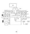
以下、最良の実施形態を添付図面を参照しながら説明する。図1は、本発明を適用できるUHF−ECR(Electron Cyclotron Resonance)を用いたプラズマエッチング装置を示す図である。UHF−ECRを用いたプラズマエッチング装置は、UHF電磁波をアンテナ102より放射し、磁場との相互作用によってプラズマを生成するUHF−ECR方式のプラズマエッチング装置である。
Hereinafter, the best embodiment will be described with reference to the accompanying drawings. FIG. 1 is a diagram showing a plasma etching apparatus using UHF-ECR (Electron Cyclotron Resonance) to which the present invention can be applied. A plasma etching apparatus using UHF-ECR is a UHF-ECR type plasma etching apparatus that emits UHF electromagnetic waves from an
このエッチング装置におけるプラズマ処理容器(この例の場合はエッチング処理容器101)は図示しない温調手段によりその内壁面を20〜100℃の温度範囲で温度調整可能となっている。エッチング処理容器101の上部にはアンテナ102が配置され、エッチング処理容器101とアンテナ102との間にはUHF電磁波を透過可能な誘電体103が設けられている。アンテナ102には、導波管104および整合器105を介して、UHF電磁波を発生する高周波電源106が接続されている。
The plasma processing container (
エッチング処理容器101の外周部にはエッチング処理容器101内に磁場を形成するための磁場コイル107が配置されている。エッチング処理容器101内のアンテナ102の下方にはウエハ108等の試料を配置するための試料台としての下部電極109が設けられている。下部電極109には、エッチング処理容器101の外にある高周波電源111が高周波バイアス整合器110を介して接続されている。
A
このように構成したプラズマエッチング装置では、高周波電源106から出力されたUHF電磁波は、整合器105、導波管104およびアンテナ102を介してエッチング処理容器101に供給される。
In the plasma etching apparatus configured as described above, the UHF electromagnetic wave output from the high-
一方、エッチング処理容器101の周囲に配置した磁場コイル107による磁界がエッチング処理容器101に形成され、前記UHF電磁波の電界と磁場コイルの磁界との相互作用によって、図示しないガス供給装置を介してエッチング処理容器101内に導入されたエッチングガスは効率良くプラズマ化される。
On the other hand, a magnetic field generated by the
図2は、このようなプラズマエッチング装置において、慣らし放電の終了を判定するための構成を説明する図である。図2において、117はデータ収集部であり、プラズマ処理中にエッチングパラメータを逐次モニタリングし、モニタリングしたデータを収集する。なお、収集するエッチングパラメータとしては、(1)プラズマ発光強度(スペクトル強度)、(2)ウエハバイアス電圧、(3)排気バルブの開度、(4)エッチング処理容器の真空排気時間、(5)整合器を構成するコンデンサの整合時容量、(6)プラズマ着火時間、(7)静電吸着電圧、(8)伝熱ガス流量、等を設定する。 FIG. 2 is a diagram illustrating a configuration for determining the end of break-in discharge in such a plasma etching apparatus. In FIG. 2, 117 is a data collection unit that sequentially monitors etching parameters during plasma processing and collects the monitored data. Etching parameters to be collected include (1) plasma emission intensity (spectrum intensity), (2) wafer bias voltage, (3) exhaust valve opening, (4) evacuation time of the etching process vessel, (5) The matching capacity of the capacitors constituting the matching unit, (6) plasma ignition time, (7) electrostatic adsorption voltage, (8) heat transfer gas flow rate, etc. are set.
119はデータベース部であり、慣らし放電の終了を判定するための判定値等を保存する。118は演算処理部であり、前記収集部117が収集したデータと前記データベース部119に保存されている判定値と比較演算する。これにより、ウェットクリーニング後に行う慣らし放電の終了時点を判定することができる。120は制御部であり、演算処理部118の出力信号を基にエッチング装置を制御する。また、前記収集部が収集したデータをもとにエッチング装置を制御する。
A
以下に、慣らし放電の終了時点を判定する例を詳述する。 Hereinafter, an example of determining the end point of break-in discharge will be described in detail.
[実施例1]
本実施例ではモニタリングするパラメータとしてプラズマ発光を選定する。なお、プラズマ発光は、エッチング処理容器101内で発生したプラズマ発光を光ファイバ121を介して導出し、導出した光を光検出器113によりモニタする。
[Example 1]
In this embodiment, plasma emission is selected as a parameter to be monitored. The plasma emission is derived from the plasma emission generated in the
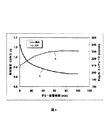
図3は第1の実施例を説明する図であり、ウエットクリーニング後に、フッ素(F)を主体とした混合ガスを用いて慣らし放電(慣らし放電は、ダミーウエハに対するプラズマ処理を、ダミーウエハを交換しながら継続して行われる。また、前記モニタリングは、例えば、各ウエハに対するプラズマ処理の終期に行われる)を行った場合において、慣らし放電の累積時間に対するエッチングレートの変化の推移を示した例である。 FIG. 3 is a diagram for explaining the first embodiment. After wet cleaning, a break-in discharge using a mixed gas mainly composed of fluorine (F) (break-in discharge is performed while plasma processing is performed on a dummy wafer while replacing the dummy wafer. Further, the monitoring is an example in which the change in the etching rate with respect to the accumulative discharge time is shown, for example, when the monitoring is performed at the end of the plasma processing for each wafer.
本実施例に使用したフッ素(F)を含む処理ガスはSF6とCHF3の混合ガスであり、流量はそれぞれ15mL/min,112mL/minである。また、処理圧力は0.4Pa、プラズマ生成用電力は800W、下部電極109に印加する高周波バイアスは15Wである。
The processing gas containing fluorine (F) used in this example is a mixed gas of SF 6 and CHF 3 , and the flow rates are 15 mL / min and 112 mL / min, respectively. The processing pressure is 0.4 Pa, the plasma generating power is 800 W, and the high frequency bias applied to the
図3において、曲線aは、試料であるウエハ(ダミーウエハ)108上に形成されたポリシリコンのエッチングレートの推移を表す。また、曲線bは、慣らし放電時の炭素(C2)および水素(H)の発光強度比(C2/H)の推移を表す。 In FIG. 3, a curve a represents transition of the etching rate of polysilicon formed on a wafer (dummy wafer) 108 as a sample. Curve b represents the transition of the emission intensity ratio (C 2 / H) of carbon (C2) and hydrogen (H) during break-in discharge.
図3に示すように、慣らし放電時間が長くなるにつれて、ポリシリコンのエッチングレートが安定することがわかる。このような現象は以下のように推測される。すなわち、慣らし放電により発生するカーボン系の反応生成物(デポ、C,CF.CH等からなる)は、その一部はプラズマ処理容器の内壁に付着し、他は排気される。 As shown in FIG. 3, it can be seen that the etching rate of polysilicon becomes stable as the break-in discharge time becomes longer. Such a phenomenon is estimated as follows. That is, a part of the carbon-based reaction product (deposited, C, CF.CH, etc.) generated by the break-in discharge adheres to the inner wall of the plasma processing vessel, and the other is exhausted.
慣らし放電が不十分な場合、即ちウエットクリーニング直後は、カーボン系デポが処理容器内壁に付着する確率が高い。このため、供給された前記混合ガス中のフッ素(F)が処理容器内壁に付着しているカーボン系デポに消費される。したがって、ウエハに供給されるフッ素(F)が減少してポリシリコンのエッチングレートが低下すると考えられる。 When the break-in discharge is insufficient, that is, immediately after wet cleaning, there is a high probability that the carbon-based deposit adheres to the inner wall of the processing container. For this reason, the fluorine (F) in the supplied mixed gas is consumed in the carbon-based deposit attached to the inner wall of the processing container. Therefore, it is considered that fluorine (F) supplied to the wafer is reduced and the etching rate of polysilicon is lowered.
一方、十分な慣らし放電を実施すると、チャンバ内壁に付着したカーボン系デポが減少するため、処理容器内壁で消費されるフッ素(F)が減少し、ウエハに供給されるフッ素(F)が増加してポリシリコンのエッチレートが増加したと考えられる。 On the other hand, if sufficient running-in discharge is performed, carbon-based deposits adhering to the inner wall of the chamber are reduced, so that fluorine (F) consumed on the inner wall of the processing vessel is reduced and fluorine (F) supplied to the wafer is increased. It is thought that the etch rate of polysilicon increased.
すなわち、図3の曲線bに示すように、プラズマ発光の発光強度比(C2/H)の推移モニタし、発光強度比(C2/H)が安定値に達したとき慣らし放電の終了と判定することができる。 That is, as shown by a curve b in FIG. 3, the transition of the emission intensity ratio (C 2 / H) of plasma emission is monitored, and when the emission intensity ratio (C 2 / H) reaches a stable value, Can be determined.
[実施例2]
図4は、第2の実施例を説明する図である。本実施例では、モニタリングするパラメータとしてウエハバイアス電圧Vpp(ピークツーピーク電圧)を選定する。
[Example 2]
FIG. 4 is a diagram for explaining the second embodiment. In this embodiment, a wafer bias voltage Vpp (peak-to-peak voltage) is selected as a parameter to be monitored.
本実施例では、3台の同一仕様のエッチング装置(装置1,装置2,装置3)を用い、それぞれのエッチング装置にウエットクリーニングを施した後、真空排気を開始する。処理容器内の圧力が0.0005Pa以下に到達するまで排気を継続する。また、処理容器内のアウトガス・レートが0.08Pa・L/sec以下であることを確認する。その後、新品のSiウエハ(ダミーウエハ)を用いて、慣らし放電を繰り返し実施しながら、高周波バイアス電源111のVpp電圧を測定した。なお、前記Vppは高周波バイアス整合器110の部分で検出する。
In this embodiment, three etching apparatuses having the same specifications (
処理条件としては、例えばプラズマ生成用電力600Wで、処理ガスとしてCl2/HBr/O2の混合ガスを用いてプラズマを生成し、高周波バイアスを50W印加した条件で処理を行った。 As processing conditions, for example, plasma was generated using a plasma generating power of 600 W, a plasma was generated using a mixed gas of Cl 2 / HBr / O 2 as a processing gas, and processing was performed under a condition where a high frequency bias of 50 W was applied.
本実施例では、前記3台のエッチング装置の処理圧力を、1.6Pa,1.2Paおよび0.4Paに設定し処理を行い、Vpp変動を前記処理圧力毎にモニタした。なお、処理容器101の圧力は圧力計114を介してモニタすることができる。
In this example, the processing pressures of the three etching apparatuses were set to 1.6 Pa, 1.2 Pa, and 0.4 Pa, and processing was performed, and Vpp fluctuation was monitored for each processing pressure. Note that the pressure in the
図4の処理圧力:1.6Paの例に示すように、ウエットクリーニング直後のVpp電圧は3台とも異なる値を示すが、慣らし放電を続けていくと、ある一定の電圧で安定していくことががわかる。この現象は以下のように推測される。すなわち、慣らし放電が不十分なときには処理容器内壁にSiとエッチングガスとの反応生成物が付着する。しかし慣らし放電が十分になると、前記処理容器内壁付着した反応生成物、あるいはウエットクリーニングの際に処理容器内に残留した水分等が除去され、装置状態が安定化したことによるとものと考えられる。 As shown in the example of the processing pressure of 1.6 Pa in FIG. 4, the Vpp voltage immediately after wet cleaning shows a different value for all three units. However, as the running-in discharge continues, the Vpp voltage becomes stable at a certain voltage. I understand. This phenomenon is presumed as follows. That is, when the break-in discharge is insufficient, a reaction product of Si and etching gas adheres to the inner wall of the processing vessel. However, if the break-in discharge is sufficient, it is considered that the reaction product adhering to the inner wall of the processing container or moisture remaining in the processing container during the wet cleaning is removed and the apparatus state is stabilized.
すなわち、下部電極に供給する高周波バイアスのピークツーピーク電圧Vppが慣らし放電の処理時間の増加とともに増加して安定値に達したとき、慣らし放電の終了と判定することができる。 That is, when the peak-to-peak voltage Vpp of the high-frequency bias supplied to the lower electrode increases with the increase of the break-in processing time and reaches a stable value, it can be determined that the break-in discharge has ended.
なお、図4に示す処理圧力:1.2Paの例、あるいは処理圧力:0.4Paの例に示すように、処理圧力が1.6Paに満たない処理条件の場合には、処理容器内壁からのアウトガス等の影響を受けにくく、Vpp変動を有効に検出することは難しくなる。 In addition, as shown in the example of the processing pressure: 1.2 Pa shown in FIG. 4 or the example of the processing pressure: 0.4 Pa, when the processing pressure is less than 1.6 Pa, the pressure from the inner wall of the processing container It is difficult to be affected by outgas and the like, and it becomes difficult to detect Vpp fluctuation effectively.
[実施例3]
図5は第3の実施例を説明する図である。本実施例では、モニタリングするパラメータとして排気バルブ115の開度(VV開度)を選定する。排気バルブ開度は、処理容器内圧力が設定圧力になるようにターボ分子ポンプ116の排気具合を調整する排気バルブの開度である。
[Example 3]
FIG. 5 is a diagram for explaining the third embodiment. In this embodiment, the opening degree (VV opening degree) of the
本実施例では、3台の同一仕様のエッチング装置(装置1,装置2,装置3)のそれぞれにウエットクリーニングを施した後、ターボ分子ポンプ116により、例えば一定流量で真空排気を開始し、処理容器内圧力が0.0005Pa以下になるまで真空排気を継続する。次いで、処理条件として、例えば処理容器内圧力を2.0Paに制御し、プラズマ生成用電力を600Wに設定し、処理ガスとしてCl2/HBr/O2の混合ガスを用いてプラズマを生成し、RFバイアスを50W印加した条件で処理を行った。試料としてはSiウエハ(ダミーウエハ)を用い、慣らし放電毎に前記処理容器圧力を2.0Paに維持するに要する排気バルブ開度を測定した。
In this embodiment, after wet cleaning is performed on each of three etching apparatuses having the same specifications (
図5の、処理圧力:2.0Paの例に示すように、ウエットクリーニング直後は、排気バルブ開度が大きいことがわかる。 As shown in the example of the processing pressure of 2.0 Pa in FIG. 5, it can be seen that the exhaust valve opening is large immediately after the wet cleaning.
慣らし放電が不十分な場合には、ウエットクリーニングにより処理容器内に残留した水分あるいは大気中の成分と反応して生成されたデポからアウトガスが生成し、生成したアウトガスが処理容器内の圧力をわずかに上昇させるためである。慣らし放電が十分になると、前記残留した水分あるいはデポが除去されて生成するアウトガスが減少する。このため、処理容器内の圧力の上昇が抑制されることにより、排気バルブ開度は小さくなる。なお、図5の、処理圧力:5.0Paの例に示すように、処理容器圧力を5.0Paに制御する場合においても、処理容器圧力を2.0Paに制御する場合と同様な傾向が得られる。 When the break-in discharge is insufficient, outgas is generated from the depot generated by reaction with moisture or atmospheric components remaining in the processing container by wet cleaning, and the generated outgas slightly reduces the pressure in the processing container. It is for raising to. When the break-in discharge is sufficient, the residual moisture or deposit is removed and the generated outgas decreases. For this reason, the exhaust valve opening is reduced by suppressing an increase in the pressure in the processing container. In addition, as shown in the example of the processing pressure of 5.0 Pa in FIG. 5, the same tendency as in the case of controlling the processing container pressure to 2.0 Pa is obtained even when the processing container pressure is controlled to 5.0 Pa. It is done.
すなわち、排気バルブ開度が、慣らし放電の処理時間の増加とともに減少して安定値に達したとき、慣らし放電の終了と判定することができる
[実施例4]
図6は、第4の実施例を説明する図である。本実施例では、モニタリングするパラメータとして、Siウエハ(ダミーウエハ)を用いた慣らし放電後に、処理容器内の残留ガスをターボ分子ポンプにより排出する際、一定圧力までに到達するに要する時間を設定し、この時間の推移を測定する。
That is, when the exhaust valve opening decreases with the increase of the running-in treatment time and reaches a stable value, it can be determined that the running-in discharge has ended (Example 4).
FIG. 6 is a diagram for explaining the fourth embodiment. In this embodiment, as a parameter to be monitored, after the break-in discharge using the Si wafer (dummy wafer), when discharging the residual gas in the processing container by the turbo molecular pump, the time required to reach a certain pressure is set, The transition of this time is measured.
この例では、2台の同一仕様のエッチング装置(装置1,装置2)にウエットクリーニングを施した後、真空排気を開始し、処理容器内の圧力を0.0005Pa以下に到達させる。このとき処理容器内のアウトガス・レートが0.08Pa・L/sec以下であることを確認した後、新品のSiウエハ(ダミーウエハ)を用いて、慣らし放電を実施した。
In this example, after wet cleaning is performed on two etching apparatuses having the same specifications (
処理条件としては、例えば処理圧力を0.4Paに制御し、プラズマ生成用電力を600Wに設定し、処理ガスとしてCl2/HBr/O2の混合ガスを用いてプラズマを生成し、RFバイアスを50W印加した条件で処理を行った。 As the processing conditions, for example, the processing pressure is controlled to 0.4 Pa, the power for plasma generation is set to 600 W, plasma is generated using a mixed gas of Cl 2 / HBr / O 2 as the processing gas, and the RF bias is set. The treatment was performed under the condition that 50 W was applied.
Siウエハ(ダミーウエハ)を用いた慣らし放電を行った後に、処理容器内の残留ガスをターボ分子ポンプ116により、例えば一定流量で排出する。このとき一定圧力(目標圧力)まで到達するに要する時間を測定する。
After the break-in discharge using the Si wafer (dummy wafer), the residual gas in the processing container is discharged by the turbo
本実施例では、到達圧力を0.005Paに設定し、この圧力に到達するまでの時間を測定した。なお、処理容器内圧力は圧力計114によりモニタすることができる。
In this example, the ultimate pressure was set to 0.005 Pa, and the time until this pressure was reached was measured. The internal pressure of the processing container can be monitored by the
図6は、前記目標圧力(0.005Pa)に到達するまでの時間(排気時間)の推移を示す図である。図6に示すように、ウエットクリーニング直後は、目標圧力までの到達時間が長いことがわかる。これは、ウエットクリーニングにより、処理容器内に残留した水分、あるいは大気中の成分と反応して生成された物質が、プラズマ放電により解離され、プラズマ放電後の排気時間に影響を与えていると考えられる。 FIG. 6 is a graph showing a transition of time (exhaust time) until the target pressure (0.005 Pa) is reached. As shown in FIG. 6, it can be seen that the time to reach the target pressure is long immediately after the wet cleaning. This is thought to be due to the fact that wet cleaning causes moisture remaining in the processing vessel or substances generated by reaction with atmospheric components to be dissociated by plasma discharge, affecting the exhaust time after plasma discharge. It is done.
なお、前記排気時間は、Siウエハ(ダミーウエハ)を用いた慣らし放電を重ねると短縮されて行き、一定の時間で安定していくようになる。これは処理容器内の状態が安定したことを示している。すなわち、図6に示すように、慣らし放電後における排気時間の推移モニタし、プラズマ放電終了後、処理容器内圧力が目標圧力に排気されるまでに要する時間が慣らし放電時間の増加とともに減少して、安定値に達したとき、慣らし放電の終了と判定することができる。 The evacuation time is shortened when the break-in discharge using the Si wafer (dummy wafer) is repeated, and becomes stable in a certain time. This indicates that the state in the processing container is stable. That is, as shown in FIG. 6, the transition of the exhaust time after the break-in discharge is monitored, and after the plasma discharge is completed, the time required for the process vessel pressure to be exhausted to the target pressure decreases as the break-in discharge time increases. When the stable value is reached, it can be determined that the break-in discharge has ended.
[実施例5]
図7,8は、第5の実施例を説明する図である。本実施例では、モニタリングするパラメータとしてプラズマ生成用高周波電源に接続した整合器105(ソースバイアス整合器)を構成するコンデンサの整合時の静電容量を設定し、該容量の変化の推移を測定する。
[Example 5]
7 and 8 are diagrams for explaining the fifth embodiment. In this embodiment, as a parameter to be monitored, an electrostatic capacitance at the time of matching of a capacitor constituting the matching unit 105 (source bias matching unit) connected to the plasma generating high frequency power source is set, and a change in the capacitance is measured. .
図7は、整合器105の構成を説明する図である。図7において、71はプラズマ生成用高周波電源106と導波管104を接続する同軸線路である。72,73,74はそれぞれ同軸線路71に接続した分岐路であり、分岐路72にはコンデンサC1、リアクトルL1からなる共振回路が挿入され、分岐路73にはコンデンサC2、リアクトルL2からなる共振回路が挿入され、分岐路74にはコンデンサC3、リアクトルL3からなる共振回路が挿入される。
FIG. 7 is a diagram for explaining the configuration of the
図7は、ウエットクリーニング後の慣らし放電時間に対する整合器105の整合時における容量(整合容量)の推移を示した図である。なお、慣らし放電に使用したハロゲンを含むガスは、Cl2/O2/HBrの混合ガスであり、流量はそれぞれ40mL/min,5mL/min,140mL/min、処理圧力は0.4Pa、プラズマ生成用電力は500W、下部電極に印加する高周波バイアスは20Wである。
FIG. 7 is a graph showing the transition of the capacity (matching capacity) during matching of the
図8(a)は整合器105を構成するコンデンサC1の整合容量の推移を示し、図8(b)はコンデンサC2の整合容量の推移を示し、図8(c)はコンデンサC3の整合容量の推移を示す。
8A shows the transition of the matching capacity of the capacitor C1 constituting the
慣らし放電時間が長くなるにつれて、図8(a)に示すコンデンサC1および図8(c)に示すコンデンサC3の整合容量は大きく変動しないのに対し、図8(b)に示すコンデンサC2の整合容量は大きく変動する。また、図6(b)に示すようにコンデンサC2の整合容量は、慣らし放電時間40分以上で安定する。 As the break-in discharge time becomes longer, the matching capacity of the capacitor C1 shown in FIG. 8 (a) and the matching capacity of the capacitor C3 shown in FIG. 8 (c) do not vary greatly, whereas the matching capacity of the capacitor C2 shown in FIG. 8 (b). Fluctuates greatly. Further, as shown in FIG. 6B, the matching capacity of the capacitor C2 is stabilized after the break-in time of 40 minutes or more.
このような現象は以下のように推測される。慣らし放電が不十分な場合、即ちウエットクリーニング直後は、残留した水分や大気中で生成されたデポがアウトガス成分となるため、処理容器内雰囲気が不安定となり、コンデンサの整合容量が安定しないと考えられる。しかし、慣らし放電が十分な場合は、慣らし放電にて生成されたデポで処理容器内雰囲気が安定することにより、コンデンサの整合容量も安定すると考えられる。このように、整合器105を構成するコンデンサの整合時の静電容量(整合容量)を検出し、検出容量がプラズマ処理時間の増加とともに増加して安定値に達したとき、慣らし放電の終了と判定することができる。
Such a phenomenon is estimated as follows. If the break-in discharge is insufficient, that is, immediately after wet cleaning, residual moisture or depot generated in the atmosphere becomes an outgas component, so the atmosphere in the processing vessel becomes unstable and the matching capacity of the capacitor is not stable. It is done. However, when the break-in discharge is sufficient, it is considered that the matching capacity of the capacitor is also stabilized by stabilizing the atmosphere in the processing container at the deposit generated by the break-in discharge. In this way, when the capacitance (matching capacitance) at the time of matching of the capacitors constituting the
[実施例6]
図9は、第6の実施例を説明する図である。本実施例では、モニタリングするパラメータとしてプラズマ着火検出時間(プラズマ生成用高周波電力を印加してからプラズマが生成するまでの時間)を設定する。
[Example 6]
FIG. 9 is a diagram for explaining the sixth embodiment. In the present embodiment, a plasma ignition detection time (a time from application of high-frequency power for generating plasma to generation of plasma) is set as a parameter to be monitored.
本実施例では、2台の同一仕様のエッチング装置(装置1,装置2)にウエットクリーニングを施した後に真空排気を開始する。処理容器内の圧力を0.0005Pa以下に設定し、その後、Siウエハ(ダミーウエハ)を順次搬入して慣らし放電を繰り返す。このとき、光検出器113により、前記プラズマ着火時間を測定する。
In this embodiment, evacuation is started after wet cleaning is performed on two etching apparatuses having the same specifications (
慣らし放電の条件として、プラズマ生成用電力を400Wに設定し、処理ガスとしてAr/CF4/CHF3/O2の混合ガスを用い、下部電極に印加する高周波バイアスとして150Wを設定した。 As conditions for the break-in discharge, the power for plasma generation was set to 400 W, a mixed gas of Ar / CF 4 / CHF 3 / O 2 was used as the processing gas, and 150 W was set as the high-frequency bias applied to the lower electrode.
図9は、ウエットクリーニング後の慣らし放電時間に対するプラズマ着火時間の推移を示した図である。図9に示すように、ウエットクリーニング直後は慣らし放電を行っても、プラズマ着火時間は装置1および装置2共に不安定である。しかし、慣らし放電を繰り返すことによりプラズマ着火時間は安定する。これは、ウエットクリーニング後に処理容器内壁に残留している水分あるいは洗浄での残留物が慣らし放電を繰り返すことにより除去され、処理容器内壁の表面状態が安定し、また、慣らし放電によるエッチング作用に伴って生成された反応生成物が処理容器内壁へ堆積し安定したことを示している。
FIG. 9 is a graph showing the transition of the plasma ignition time with respect to the break-in discharge time after wet cleaning. As shown in FIG. 9, the plasma ignition time is unstable in both the
すなわち、処理容器にプラズマ生成用高周波電力を供給してから、プラズマが着火するまでの時間を検出し、該時間がプラズマ処理時間の増加とともに減少して安定値に達したとき、慣らし放電の終了と判定することができる。 That is, the time from supplying high-frequency power for generating plasma to the processing vessel until the plasma is ignited is detected, and when the time decreases with increasing plasma processing time and reaches a stable value, the break-in discharge ends. Can be determined.
[実施例7]
図10は、第7の実施例を説明する図である。本実施例では、モニタリングするパラメータとして静電吸着電圧(ESC電圧)を設定する。なお、静電吸着電圧は静電吸着電源112が発生する直流電圧であり、ウエハ108を下部電極109に静電吸着させる電圧である。静電吸着電圧は、静電吸着用電源112の電源電圧が一定であっても電源の内部抵抗により変動する。すなわち静電吸着電流の変動に応じて変動する。
[Example 7]
FIG. 10 is a diagram for explaining the seventh embodiment. In this embodiment, an electrostatic adsorption voltage (ESC voltage) is set as a parameter to be monitored. The electrostatic chucking voltage is a DC voltage generated by the electrostatic
本実施例では、3台の同一仕様のエッチング装置(装置1,装置2,装置3)のそれぞれにウエットクリーニングを施した後、ターボ分子ポンプ116により真空排気を開始し、処理容器内圧力が0.0005Pa以下になるまで真空排気を継続する。次いで、処理条件として、例えば処理容器内圧力を2.0Paに制御し、プラズマ生成用電力を600Wに設定し、処理ガスとしてCl2/HBr/O2の混合ガスを用いてプラズマを生成し、RFバイアスを50W印加した条件で処理を行った。
In this embodiment, after performing wet cleaning on each of the three etching apparatuses having the same specifications (
図10は、静電吸着電圧の時間推移を示す図である。図に示すように、ウエットクリーニング直後は静電吸着電圧が小さくて、慣らし放電が十分になるにつれて、静電吸着電圧が安定する。この現象は以下のように推測する。慣らし放電が不十分なときはウエットクリーニングによる残留水分あるいは反応生成物からのアウトガスにより、放電が不安定になる。このため、静電吸着電圧は小さく、その値もばらつく。慣らし放電が十分になると、前記残留水分あるいは前記反応生成物は除去され、アウトガスが減少して、プラズマは安定する。これにより静電吸着電圧が安定する。 FIG. 10 is a diagram illustrating a time transition of the electrostatic adsorption voltage. As shown in the figure, the electrostatic adsorption voltage is small immediately after the wet cleaning, and the electrostatic adsorption voltage becomes stable as the break-in discharge becomes sufficient. This phenomenon is estimated as follows. When the break-in discharge is insufficient, the discharge becomes unstable due to residual moisture by wet cleaning or outgas from the reaction product. For this reason, the electrostatic adsorption voltage is small and its value varies. When the break-in discharge is sufficient, the residual moisture or the reaction product is removed, the outgas is reduced, and the plasma is stabilized. This stabilizes the electrostatic adsorption voltage.
このように、下部電極に供給する静電吸着電圧のばらつきがプラズマ処理時間の増加とともに減少し、かつ前記静電吸着電圧が増加して安定値に達したとき、慣らし放電の終了と判定することができる。 Thus, when the variation in the electrostatic adsorption voltage supplied to the lower electrode decreases as the plasma processing time increases and the electrostatic adsorption voltage increases to reach a stable value, it is determined that the break-in discharge has ended. Can do.
[実施例8]
本実施例では、モニタするパラメータとして下部電極と該下部電極上に載置したウエハ間に供給する伝熱ガスの流量を設定する。伝熱ガス(He)の流量は、ウエットクリーニング直後は大きくて、慣らし放電が十分になるにつれて、減少して安定する。
[Example 8]
In this embodiment, the flow rate of the heat transfer gas supplied between the lower electrode and the wafer placed on the lower electrode is set as a parameter to be monitored. The flow rate of the heat transfer gas (He) is large immediately after wet cleaning, and decreases and stabilizes as the break-in discharge becomes sufficient.
本実施例では、3台の同一仕様のエッチング装置のそれぞれにウエットクリーニングを施した後、ターボ分子ポンプ116により真空排気を開始し、処理容器内圧力が0.0005Pa以下になるまで真空排気を継続する。次いで、処理条件として、例えば処理容器内圧力を2.0Paに制御し、プラズマ生成用電力を600Wに設定し、処理ガスとしてCl2/HBr/O2の混合ガスを用いてプラズマを生成し、RFバイアスを50W印加した条件で処理を行った。
In this embodiment, after performing wet cleaning on each of the three etching apparatuses of the same specification, evacuation is started by the turbo
ウエットクリーニング後、Siウエハ(ダミーウエハ)を用いて慣らし放電を繰り返し実施しすることにより、下部電極のヘッド部の残留水分が除去され、また、下部電極表面の外周部が反応生成物に覆われてウエハの吸着力が回復する。これにより、伝熱ガスの流量が減少して安定するものと考えられる。 なお、伝熱ガスの流量に代えて伝熱ガスの圧力(ウエハの裏面側における圧力)の推移を利用することができる。 After wet cleaning, repeated running-in using a Si wafer (dummy wafer) removes residual moisture from the head portion of the lower electrode, and the outer peripheral portion of the lower electrode surface is covered with reaction products. The wafer adsorption force is restored. Thereby, it is thought that the flow rate of the heat transfer gas decreases and stabilizes. Instead of the flow rate of the heat transfer gas, the transition of the pressure of the heat transfer gas (pressure on the back side of the wafer) can be used.
すなわち、下部電極と該下部電極上に載置した試料間に供給する伝熱ガスの流量を検出し、該流量がプラズマ処理時間の増加とともに減少して安定値に達したとき、慣らし放電の終了と判定することができる。 That is, the flow rate of the heat transfer gas supplied between the lower electrode and the sample placed on the lower electrode is detected, and when the flow rate decreases with increasing plasma processing time and reaches a stable value, the break-in discharge ends. Can be determined.
以上説明したように、各実施例において慣らし放電の終了と判定した時点、すなわち、(1)プラズマ中の炭素C2と水素Hの発光強度比(C2/H)が減少して安定値に達したとき、
(2)下部電極に供給する高周波バイアスのピークツーピーク電圧がプラズマ処理時間の増加とともに増加して安定値に達したとき、
(3)プラズマ処理中における前記排気バルブの開度がプラズマ処理時間の増加とともに減少してて安定値に達したとき、
(4)プラズマ放電終了後、処理容器内圧力が所定真空圧に排気されるまでに要する時間がプラズマ処理時間の増加とともに減少して安定値に達したとき、
(5)整合器を構成するコンデンサの整合動作時の静電容量がプラズマ処理時間の増加とともに増加して安定値に達したとき、
(6)アンテナ電極に整合器を介して高周波電力を供給してから、プラズマが着火するまでの時間がプラズマ処理時間の増加とともに減少して安定値に達したとき、
(7)下部電極に供給する静電吸着電圧のばらつきがプラズマ処理時間の増加とともに減少し、かつ前記静電吸着電圧が増加して安定値に達したとき、
(8)下部電極と該下部電極上に載置した試料間に供給する伝熱ガスの流量がプラズマ処理時間の増加とともに減少して安定値に達したとき、
はいずれもウエットクリーニングの際に付着した水分(残留水分)等に基づくアウトガスの供給が消失した時点、あるいは装置に所定量の反応生成物が付着して装置が安定化した時点、に密接に関連していると考えられる。
As described above, when it is determined that the break-in discharge is finished in each example, that is, (1) the emission intensity ratio (C 2 / H) of carbon C 2 and hydrogen H in the plasma decreases to a stable value. When you reach
(2) When the peak-to-peak voltage of the high frequency bias supplied to the lower electrode increases as the plasma processing time increases and reaches a stable value,
(3) When the opening of the exhaust valve during plasma processing decreases with increasing plasma processing time and reaches a stable value,
(4) When the time required for the pressure in the processing vessel to be exhausted to a predetermined vacuum pressure after the plasma discharge is finished decreases with the increase of the plasma processing time and reaches a stable value,
(5) When the capacitance at the matching operation of the capacitors constituting the matching unit increases with the increase of the plasma processing time and reaches a stable value,
(6) When the time from when high frequency power is supplied to the antenna electrode via the matching unit until the plasma is ignited decreases with increasing plasma processing time and reaches a stable value,
(7) When the variation in the electrostatic adsorption voltage supplied to the lower electrode decreases as the plasma processing time increases, and the electrostatic adsorption voltage increases to reach a stable value,
(8) When the flow rate of the heat transfer gas supplied between the lower electrode and the sample placed on the lower electrode decreases with increasing plasma processing time and reaches a stable value,
Are closely related to the point at which the outgas supply based on moisture (residual moisture) attached during wet cleaning disappears, or the point when a predetermined amount of reaction product adheres to the device and the device stabilizes. it seems to do.
したがって、少なくとも前記アウトガスに伴う処理室内圧力の上昇(排気に要する時間の増大)を間接的に測定することで慣らし放電の終了時点を判定することができる。このため、以上に説明した各実施例では、慣らし放電中に、ある特定の物理量(パラメータ)が慣らし放電時間の経過と共に変化し、その後安定することを利用して、慣らし放電の終点を判定している。 Therefore, it is possible to determine the end point of the break-in discharge by indirectly measuring at least an increase in the pressure in the processing chamber (an increase in time required for exhaust) accompanying the outgas. For this reason, in each of the embodiments described above, the end point of the break-in discharge is determined using the fact that a specific physical quantity (parameter) changes during the break-in discharge time and then stabilizes during the break-in discharge. ing.
前記物理量が安定したと判定する基準の設定に際して、発明者らは、事前に数多く実験を行い、前記物理量がどのように推移するかを記録した。 When setting the standard for determining that the physical quantity is stable, the inventors conducted a number of experiments in advance and recorded how the physical quantity changes.
前記実験結果によれば、ウエットクリーニング後に慣らし放電を継続した場合、毎回安定して一定値になるパラメータもあれば、ウエットクリーニング毎に安定する値が異なるパラメータもある。 According to the experimental results, there are parameters that become stable and constant each time when the break-in discharge is continued after wet cleaning, and there are parameters that have different values that stabilize every wet cleaning.
例えば、前記パラメータの値が、関係する部品の消耗度等に影響されない場合には、ウエットクリーニング毎にパラメータの安定する値が変化することはない(例えば、実施例2,3,4,5,6,7,8)。 For example, when the parameter value is not affected by the degree of wear or the like of related parts, the stable value of the parameter does not change every wet cleaning (for example, Examples 2, 3, 4, 5, 6, 7, 8).
一方、前記パラメータの値が、関係する部品の消耗度等に影響される場合には、ウエットクリーニング毎にパラメータの安定する値が異なることになる(例えば、実施例1)。 On the other hand, when the parameter value is affected by the degree of wear of related parts, the stable parameter value differs for each wet cleaning (for example, Example 1).
前者の場合(パラメータの値が毎回再現する場合)には、終点判定においてはパラメータの値がある閾値を超える(あるいは下回る)ことにより判定できる。この判定方法を以下、レベル判定と呼ぶこととする。 In the former case (when the parameter value is reproduced every time), the end point can be determined by exceeding (or falling below) a certain threshold value. Hereinafter, this determination method is referred to as level determination.
また、後者の場合(パラメータの値が毎回異なる場合)には、ある特定時点のパラメータの値を単独に用いるのみでは終点判定が行えない。このため、何度か実施する慣らし放電中のパラメータの変化量をチェックすることにより終点判定を行う必要がある。このような判定は従来よりプラズマ発光を用いたエッチング終点判定では実施されている。この方法では、パラメータの1次、もしくは2次微分値を計算し、その変化量により判定を行う。以下、この方法を1次、2次あわせて微分判定法と呼ぶ。 In the latter case (when the parameter values are different each time), the end point cannot be determined only by using the parameter values at a specific time point alone. For this reason, it is necessary to determine the end point by checking the amount of parameter change during the break-in discharge that is performed several times. Such determination is conventionally performed in the etching end point determination using plasma emission. In this method, a first-order or second-order differential value of a parameter is calculated and a determination is made based on the amount of change. Hereinafter, this method is referred to as a differential determination method by combining the first order and second order.
図11は、レベル判定法の原理を説明する図である。図11に示すように、慣らし放電時間の経過とともにパラメータの値が変化し、安定領域において安定する。ウエットクリーニング毎にこのように安定領域で安定し、その再現性が十分である場合には、安定領域における安定値の、例えば90%を越えた時点を慣らし放電の終点とすることができる。なお、この終点では、実際には未だ安定領域に入ってないので、実運用では終点判定後さらに一定のダミー放電時間を追加するとよい。 FIG. 11 is a diagram for explaining the principle of the level determination method. As shown in FIG. 11, the parameter value changes with the passage of the break-in discharge time, and is stabilized in the stable region. When stable in the stable region at each wet cleaning and the reproducibility is sufficient, the time point when the stable value in the stable region exceeds 90%, for example, can be used as the end point of the break-in discharge. It should be noted that at this end point, since it has not actually entered the stable region, a certain dummy discharge time may be added after the end point determination in actual operation.
図12は微分法の原理を説明する図である。図12(a)に示すように推移するパラメータを1次微分すると図12(b)に示す1次微分値が得られ、2次微分すると図12(c)に示す2次微分値が得られる。このようにして得られた1次微分値あるいは2次微分値を閾値と比較して慣らし放電の終点を判定する。終点判定に際しては、誤判定防止用のデッドタイムを設定し、設定したデッドタイム経過した後の1次微分値あるいは2次微分値と閾値を比較して判定する。 FIG. 12 is a diagram for explaining the principle of the differential method. As shown in FIG. 12 (a), the first-order differentiation of the transition parameter yields the first-order differential value shown in FIG. 12 (b), and the second-order differentiation yields the second-order differential value shown in FIG. 12 (c). . The end point of the break-in discharge is determined by comparing the primary differential value or the secondary differential value thus obtained with a threshold value. When determining the end point, a dead time for preventing erroneous determination is set, and the primary differential value or the secondary differential value after the set dead time elapses is compared with a threshold value for determination.
図12(b)の例では、1次微分値が閾値を下回った場合、パラメータの変動が小さくなったことを表しているため、1次微分値が閾値を下回った時点を終点と判定する。 In the example of FIG. 12B, when the primary differential value falls below the threshold value, it indicates that the fluctuation of the parameter has become small. Therefore, the time point when the primary differential value falls below the threshold value is determined as the end point.
図12(c)の例では、2次微分値が閾値1を下回り、次いで閾値2を超えた時点を終点と判定する。2次微分値の極大、極小値は元の信号の変曲点を表すため、前述のように2次微分値と閾値を2度比較することにより、元の信号が一定状態から上昇に転じ、再度一定値に安定したことがわかる。
In the example of FIG. 12C, the time when the secondary differential value falls below the
[実施例9]
本実施例では、モニタするパラメータとして前記実施例1ないし8においてモニタしたパラメータの全てをモニタする。すなわち、前記各実施例においてモニタしたパラメータは、ダミーウエハを用いた慣らし放電中に、同時にモニタすることができる。したがって実施例1ないし8の各々に開示した方法により慣らし放電の終点を検出することが可能であるが、すべての項目を用いて総合的に判定することもできる。以下に総合判定の例(総合判定例1,2,3)を図13,14,15を参照して説明する。
[Example 9]
In this embodiment, all parameters monitored in the first to eighth embodiments are monitored as parameters to be monitored. That is, the parameters monitored in each of the above embodiments can be monitored simultaneously during the break-in discharge using the dummy wafer. Therefore, the end point of the break-in discharge can be detected by the method disclosed in each of Examples 1 to 8, but it can also be comprehensively determined using all items. Hereinafter, examples of comprehensive determination (comprehensive determination examples 1, 2, and 3) will be described with reference to FIGS.
(総合判定例1)
図13は総合判定例1を説明する図である。この例では、まずモニタする項目(パラメータ)毎に点数を付与する。次に、モニタした項目毎に慣らし放電の終点が判定できたか否かを判別し、終点が判定できた項目に対して付与された前記点数のみを累積加算する。
(Comprehensive judgment example 1)
FIG. 13 is a diagram for explaining the comprehensive determination example 1. In this example, first, a score is assigned to each item (parameter) to be monitored. Next, it is determined whether or not the end point of the break-in discharge has been determined for each monitored item, and only the points given to the item for which the end point has been determined are cumulatively added.
図13の例では、各項目毎に各10点を付与し、終点が判定できた項目(1,2,6,7,8)に付与された点数を累積加算する。この例では、終点が判定できた項目が5項目あるので累積加算値は50点となる。また、モニタする項目は8項目あるので合計点数は最大80点となる。このうち、例えば60点獲得すれば、その時点で総合判定として慣らし放電が終了したものとすることができる。 In the example of FIG. 13, 10 points are assigned to each item, and the points assigned to the items (1, 2, 6, 7, 8) for which the end point can be determined are cumulatively added. In this example, since there are five items whose end point can be determined, the cumulative added value is 50 points. In addition, since there are 8 items to be monitored, the total score is a maximum of 80 points. Of these, for example, if 60 points are acquired, it is assumed that the break-in discharge has been completed as a comprehensive determination at that time.
(総合判定例2)
図14は総合判定例2を説明する図である。この例では、まずモニタする項目(パラメータ)毎に重み係数を付与する。また、図13の例と同様に各項目に10点を付与しておく。次に、モニタした項目毎に慣らし放電の終点が判定できたか否かを判別し、終点が判定できた項目に対して付与された前記点数のみに前記重み係数を積算して累積加算する。
(Comprehensive judgment example 2)
FIG. 14 is a diagram for explaining the comprehensive determination example 2. In this example, a weighting coefficient is first assigned to each item (parameter) to be monitored. Also, 10 points are assigned to each item as in the example of FIG. Next, it is determined whether or not the end point of the break-in discharge has been determined for each monitored item, and the weighting coefficient is integrated and cumulatively added only to the number of points given to the item for which the end point has been determined.
図14の例では、各項目毎に各10点を付与し、更に図に示す重み係数を付与する。次に終点が判定できた項目(1,2,6,7,8)に付与された点数に重み係数を累積加算する。この例では、終点が判定できた項目が5項目あるので累積加算値は80点となる。また、モニタする項目は8項目あるので合計点数は最大135点となる。このうち、例えば90点獲得すれば、その時点で総合判定として慣らし放電が終了したものとすることができる。なお、この例では合計点が最大135点となるため、適当に正規化を行うとよい。 In the example of FIG. 14, 10 points are assigned to each item, and the weighting coefficient shown in the figure is further given. Next, a weighting factor is cumulatively added to the points assigned to the items (1, 2, 6, 7, 8) for which the end point has been determined. In this example, since there are five items whose end point can be determined, the cumulative added value is 80 points. Further, since there are 8 items to be monitored, the total score is a maximum of 135 points. Among these, for example, if 90 points are acquired, it can be assumed that the break-in discharge is completed as a comprehensive determination at that time. In this example, since the total number is 135 at the maximum, normalization may be performed appropriately.
(総合判定例3)
図15は総合判定例3を説明する図である。前述のレベル判定法では、現在の値が目標値の何パーセントかという途中経過の値を得ることができる。
(Comprehensive judgment example 3)
FIG. 15 is a diagram for explaining the comprehensive determination example 3. In the above-described level determination method, it is possible to obtain an intermediate value indicating what percentage of the target value the current value is.
したがって、この例では、モニタしたパラメータの中で、そのレベルが測定可能なものについては、測定したレベルに応じて進行度(0ないし100%)を付与するようにした。 Therefore, in this example, among the monitored parameters, if the level can be measured, the degree of progress (0 to 100%) is given according to the measured level.
図15の例では、まずモニタする項目(パラメータ)毎に重み係数を付与する。また、図13の例と同様に各項目に10点を付与しておく。次に、モニタした項目毎に慣らし放電の終点が判定できたか否かを判別し、終点が判定できた項目に対して付与された前記点数のみに前記重み係数および進行度を積算して累積加算する。すなわち、(点数=10(点)×(進行度÷100)×係数)で計算する。なお、進行度に「−」表記のあるものは微分判定によるものであることを表している。 In the example of FIG. 15, a weighting coefficient is first assigned to each item (parameter) to be monitored. Also, 10 points are assigned to each item as in the example of FIG. Next, it is determined whether or not the end point of the break-in discharge has been determined for each monitored item, and the weighting factor and the degree of progress are added only to the points given to the item for which the end point has been determined, and cumulative addition is performed. To do. That is, it is calculated by (number of points = 10 (points) × (progress degree ÷ 100) × coefficient). In addition, the thing with "-" notation in the degree of progress represents that it is based on differential determination.
このように、重み係数および進行度を加味して総合判定することにより、より細かな総合判定が行えるようになり、余分な慣らし電時間を削減し、更に慣らし放電に使用するダミーウエハを節約することができる。 In this way, it is possible to make a finer overall judgment by comprehensively considering the weighting factor and the degree of progress, thereby reducing the extra running-in time and further saving dummy wafers used for the running-in discharge. Can do.
以上説明したように、エッチングパラメータの時間推移をモニタリングする機構を有し、モニタリングしたエッチングパラメータを予め設定した判定値と比較演算して、エッチング装置を制御する機構を制御するので、ウエットクリーニング後の慣らし放電の終了を高精度に判定して慣らし放電を終了することができる。これにより、 慣らし放電を必要最低限の処理枚数にすることができ、半導体製造装置の不稼動時間を短縮し、製造コストを低減することができる。 As described above, it has a mechanism for monitoring the time transition of etching parameters, and compares the calculated etching parameters with preset judgment values to control the mechanism for controlling the etching apparatus. The end of the break-in discharge can be determined with high accuracy to end the break-in discharge. As a result, the break-in discharge can be reduced to the minimum required number of processing, the downtime of the semiconductor manufacturing apparatus can be shortened, and the manufacturing cost can be reduced.
101 エッチング処理容器(プラズマ処理容器)
102 アンテナ
103 誘電体
104 導波管
105 整合器
106 プラズマ生成用高周波電源(UHF電源)
107 磁場コイル
108 ウエハ(試料)
109 下部電極(試料台)
110 高周波バイアス整合器
111 高周波バイアス電源
112 静電吸着用電源
113 光検出器
114 圧力計
115 排気バルブ
116 ターボ分子ポンプ
117 データ収集部
118 演算処理部
119 データベース部
120 制御部
121 光ファイバ
101 Etch processing vessel (plasma processing vessel)
102
104 Waveguide
105 matcher
106 High frequency power supply for plasma generation (UHF power supply)
107
109 Lower electrode (sample stage)
110 RF
DESCRIPTION OF
Claims (2)
前記プラズマ処理容器内に処理ガスを供給するガス供給装置と、
前記プラズマ処理容器内に供給された前記処理ガスを排気バルブを介して排気する排気ポンプと、
アンテナ電極に整合器を介して高周波電力を供給する高周波電源と、
前記下部電極に高周波バイアスを供給する高周波バイアス電源とを備えるプラズマ処理装置を用いて前記試料にプラズマ処理を施す処理を、複数の試料に対して順次繰り返す慣らし放電を行うプラズマ処理方法において、
次の条件(1)ないし(6)のうち複数の条件が成立したとき慣らし放電の終了と判定することを特徴とするプラズマ処理方法。
(1)プラズマ中の炭素C2と水素Hの発光強度比(C2/H)が減少して予め設定された慣らし放電の終了と判定する判定値に達したとき、
(2)下部電極に供給する高周波バイアスのピークツーピーク電圧がプラズマ処理時間の増加とともに増加して予め設定された慣らし放電の終了と判定する判定値に達したとき、
(3)プラズマ処理中における前記排気バルブの開度がプラズマ処理時間の増加とともに減少して予め設定された慣らし放電の終了と判定する判定値に達したとき、
(4)プラズマ放電終了後、処理容器内圧力が所定真空圧に排気されるまでに要する時間がプラズマ処理時間の増加とともに減少して予め設定された慣らし放電の終了と判定する判定値に達したとき、
(5)前記整合器を構成するコンデンサの整合動作時の静電容量がプラズマ処理時間の増加とともに増加して予め設定された慣らし放電の終了と判定する判定値に達したとき、
(6)前記アンテナ電極に整合器を介して高周波電力を供給してから、プラズマが着火するまでの時間がプラズマ処理時間の増加とともに減少して予め設定された慣らし放電の終了と判定する判定値に達したとき、 A plasma processing chamber having a lower electrode inside for placing a specimen,
A gas supply device for supplying a processing gas into the plasma processing vessel ;
An exhaust pump for exhausting the processing gas supplied into the plasma processing vessel through an exhaust valve;
A high frequency power supply for supplying high-frequency power through a matching unit to the antenna electrode,
In a plasma processing method of performing a break-in discharge that sequentially repeats a plurality of samples by performing a plasma processing on the sample using a plasma processing apparatus including a high-frequency bias power source that supplies a high-frequency bias to the lower electrode ,
A plasma processing method, characterized in that when a plurality of conditions among the following conditions (1) to (6) are satisfied, it is determined that the break-in discharge has ended.
(1) When the emission intensity ratio (C2 / H) of carbon C2 and hydrogen H in the plasma decreases and reaches a predetermined determination value for determining the end of the break-in discharge ,
(2) When the peak-to-peak voltage of the high-frequency bias supplied to the lower electrode increases as the plasma processing time increases and reaches a preset determination value for determining the end of the break-in discharge ,
(3) When the opening degree of the exhaust valve during plasma processing decreases as the plasma processing time increases and reaches a preset judgment value for determining the end of break-in discharge ,
(4) After the plasma discharge is completed, the time required for the pressure in the processing vessel to be exhausted to a predetermined vacuum pressure decreases with the increase of the plasma processing time, and reaches a predetermined judgment value for determining the end of the break-in discharge . When
(5) When the capacitance during the matching operation of the capacitor constituting the matching unit increases with the increase of the plasma processing time and reaches a predetermined determination value for determining the end of the break-in discharge ,
(6) A determination value for determining the end of the break-in discharge set in advance by reducing the time from when high-frequency power is supplied to the antenna electrode through the matching unit to when the plasma is ignited as the plasma processing time increases. When we reach
前記プラズマ処理容器内に処理ガスを供給するガス供給装置と、
前記プラズマ処理容器内に供給された前記処理ガスを排気バルブを介して排気する排気ポンプと、
アンテナ電極に整合器を介して高周波電力を供給する高周波電源と、
前記下部電極に高周波バイアスを供給する高周波バイアス電源とを備え、
前記試料にプラズマ処理を施す処理を、複数の試料に対して順次繰り返す慣らし放電を行うプラズマ処理装置において、
次の条件(1)ないし(6)のうち複数の条件が成立したとき慣らし放電の終了と判定することを特徴とするプラズマ処理装置。
(1)プラズマ中の炭素C2と水素Hの発光強度比(C2/H)が減少して予め設定された慣らし放電の終了と判定する判定値に達したとき、
(2)下部電極に供給する高周波バイアスのピークツーピーク電圧がプラズマ処理時間の増加とともに増加して予め設定された慣らし放電の終了と判定する判定値に達したとき、
(3)プラズマ処理中における前記排気バルブの開度がプラズマ処理時間の増加とともに減少して予め設定された慣らし放電の終了と判定する判定値に達したとき、
(4)プラズマ放電終了後、処理容器内圧力が所定真空圧に排気されるまでに要する時間がプラズマ処理時間の増加とともに減少して予め設定された慣らし放電の終了と判定する判定値に達したとき、
(5)前記整合器を構成するコンデンサの整合動作時の静電容量がプラズマ処理時間の増加とともに増加して予め設定された慣らし放電の終了と判定する判定値に達したとき、
(6)前記アンテナ電極に整合器を介して高周波電力を供給してから、プラズマが着火するまでの時間がプラズマ処理時間の増加とともに減少して予め設定された慣らし放電の終了と判定する判定値に達したとき、 A plasma processing chamber having a lower electrode inside for placing a specimen,
A gas supply device for supplying a processing gas into the plasma processing vessel ;
An exhaust pump for exhausting the processing gas supplied into the plasma processing vessel through an exhaust valve;
A high frequency power supply for supplying high-frequency power through a matching unit to the antenna electrode,
A high frequency bias power supply for supplying a high frequency bias to the lower electrode ,
In the plasma processing apparatus for performing a break-in discharge that sequentially repeats the processing for performing the plasma processing on the sample for a plurality of samples,
A plasma processing apparatus, characterized in that when a plurality of conditions among the following conditions (1) to (6) are satisfied, it is determined that the break-in discharge has ended.
(1) When the emission intensity ratio (C2 / H) of carbon C2 and hydrogen H in the plasma decreases and reaches a predetermined determination value for determining the end of the break-in discharge,
(2) When the peak-to-peak voltage of the high-frequency bias supplied to the lower electrode increases as the plasma processing time increases and reaches a preset determination value for determining the end of the break-in discharge,
(3) When the opening degree of the exhaust valve during plasma processing decreases as the plasma processing time increases and reaches a preset judgment value for determining the end of break-in discharge,
(4) After the plasma discharge is completed, the time required for the pressure in the processing vessel to be exhausted to a predetermined vacuum pressure decreases with the increase of the plasma processing time, and reaches a predetermined judgment value for determining the end of the break-in discharge. When
(5) When the capacitance during the matching operation of the capacitor constituting the matching unit increases with the increase of the plasma processing time and reaches a predetermined determination value for determining the end of the break-in discharge,
(6) A determination value for determining the end of the break-in discharge set in advance by reducing the time from when high-frequency power is supplied to the antenna electrode through the matching unit to when the plasma is ignited as the plasma processing time increases. When we reach
Priority Applications (6)
| Application Number | Priority Date | Filing Date | Title |
|---|---|---|---|
| JP2006152305A JP4914119B2 (en) | 2006-05-31 | 2006-05-31 | Plasma processing method and plasma processing apparatus |
| KR1020060075692A KR100780021B1 (en) | 2006-05-31 | 2006-08-10 | Plasma processing method and plasma processing apparatus |
| TW095129644A TW200744129A (en) | 2006-05-31 | 2006-08-11 | Plasma processing method and apparatus thereof |
| US11/502,416 US8038896B2 (en) | 2006-05-31 | 2006-08-11 | Plasma processing method and apparatus |
| US12/846,403 US8900401B2 (en) | 2006-05-31 | 2010-07-29 | Plasma processing method and apparatus |
| US14/508,859 US9230782B2 (en) | 2006-05-31 | 2014-10-07 | Plasma processing method and apparatus |
Applications Claiming Priority (1)
| Application Number | Priority Date | Filing Date | Title |
|---|---|---|---|
| JP2006152305A JP4914119B2 (en) | 2006-05-31 | 2006-05-31 | Plasma processing method and plasma processing apparatus |
Publications (3)
| Publication Number | Publication Date |
|---|---|
| JP2007324341A JP2007324341A (en) | 2007-12-13 |
| JP2007324341A5 JP2007324341A5 (en) | 2009-06-18 |
| JP4914119B2 true JP4914119B2 (en) | 2012-04-11 |
Family
ID=38790792
Family Applications (1)
| Application Number | Title | Priority Date | Filing Date |
|---|---|---|---|
| JP2006152305A Expired - Fee Related JP4914119B2 (en) | 2006-05-31 | 2006-05-31 | Plasma processing method and plasma processing apparatus |
Country Status (4)
| Country | Link |
|---|---|
| US (3) | US8038896B2 (en) |
| JP (1) | JP4914119B2 (en) |
| KR (1) | KR100780021B1 (en) |
| TW (1) | TW200744129A (en) |
Families Citing this family (29)
| Publication number | Priority date | Publication date | Assignee | Title |
|---|---|---|---|---|
| JP4914119B2 (en) * | 2006-05-31 | 2012-04-11 | 株式会社日立ハイテクノロジーズ | Plasma processing method and plasma processing apparatus |
| US9157151B2 (en) * | 2006-06-05 | 2015-10-13 | Applied Materials, Inc. | Elimination of first wafer effect for PECVD films |
| KR100816453B1 (en) * | 2006-06-28 | 2008-03-27 | (주)쎄미시스코 | Real time leak detection system of process chamber |
| JP2009231718A (en) * | 2008-03-25 | 2009-10-08 | Renesas Technology Corp | Method for detecting dry etching endpoint |
| US8393197B2 (en) * | 2008-07-24 | 2013-03-12 | Pivotal Systems Corporation | Method and apparatus for the measurement of atmospheric leaks in the presence of chamber outgassing |
| JP5160393B2 (en) * | 2008-12-16 | 2013-03-13 | 東京エレクトロン株式会社 | Plasma processing method, plasma processing apparatus, and moisture detection method for plasma processing apparatus |
| JP2010165738A (en) * | 2009-01-13 | 2010-07-29 | Hitachi High-Technologies Corp | Method for seasoning plasma processing apparatus, and method for determining end point of seasoning |
| US20100332010A1 (en) * | 2009-06-30 | 2010-12-30 | Brian Choi | Seasoning plasma processing systems |
| KR101604844B1 (en) * | 2009-12-16 | 2016-03-18 | 주성엔지니어링(주) | Substrate treatment appratus and method of treating substrate using the same |
| JP5397215B2 (en) * | 2009-12-25 | 2014-01-22 | ソニー株式会社 | Semiconductor manufacturing apparatus, semiconductor device manufacturing method, simulation apparatus, and simulation program |
| JP6078419B2 (en) * | 2013-02-12 | 2017-02-08 | 株式会社日立ハイテクノロジーズ | Control method of plasma processing apparatus, plasma processing method and plasma processing apparatus |
| US10386828B2 (en) | 2015-12-17 | 2019-08-20 | Lam Research Corporation | Methods and apparatuses for etch profile matching by surface kinetic model optimization |
| US9792393B2 (en) | 2016-02-08 | 2017-10-17 | Lam Research Corporation | Methods and apparatuses for etch profile optimization by reflectance spectra matching and surface kinetic model optimization |
| US10032681B2 (en) | 2016-03-02 | 2018-07-24 | Lam Research Corporation | Etch metric sensitivity for endpoint detection |
| US10197908B2 (en) | 2016-06-21 | 2019-02-05 | Lam Research Corporation | Photoresist design layout pattern proximity correction through fast edge placement error prediction via a physics-based etch profile modeling framework |
| KR102543349B1 (en) * | 2016-07-11 | 2023-06-30 | 삼성전자주식회사 | Plasma monitoring apparatus |
| US10730082B2 (en) * | 2016-10-26 | 2020-08-04 | Varian Semiconductor Equipment Associates, Inc. | Apparatus and method for differential in situ cleaning |
| US10254641B2 (en) | 2016-12-01 | 2019-04-09 | Lam Research Corporation | Layout pattern proximity correction through fast edge placement error prediction |
| US10534257B2 (en) | 2017-05-01 | 2020-01-14 | Lam Research Corporation | Layout pattern proximity correction through edge placement error prediction |
| JP6772117B2 (en) | 2017-08-23 | 2020-10-21 | 株式会社日立ハイテク | Etching method and etching equipment |
| WO2019053836A1 (en) * | 2017-09-14 | 2019-03-21 | 株式会社日立ハイテクノロジーズ | Plasma processing device and wet cleaning method |
| US10134569B1 (en) * | 2017-11-28 | 2018-11-20 | Lam Research Corporation | Method and apparatus for real-time monitoring of plasma chamber wall condition |
| US10572697B2 (en) | 2018-04-06 | 2020-02-25 | Lam Research Corporation | Method of etch model calibration using optical scatterometry |
| US11624981B2 (en) | 2018-04-10 | 2023-04-11 | Lam Research Corporation | Resist and etch modeling |
| US11921433B2 (en) | 2018-04-10 | 2024-03-05 | Lam Research Corporation | Optical metrology in machine learning to characterize features |
| US10896833B2 (en) | 2018-05-09 | 2021-01-19 | Applied Materials, Inc. | Methods and apparatus for detecting an endpoint of a seasoning process |
| US10977405B2 (en) | 2019-01-29 | 2021-04-13 | Lam Research Corporation | Fill process optimization using feature scale modeling |
| WO2020217266A1 (en) | 2019-04-22 | 2020-10-29 | 株式会社日立ハイテクノロジーズ | Plasma processing method and plasma processing device |
| US11875978B2 (en) | 2020-06-16 | 2024-01-16 | Hitachi High-Tech Corporation | Plasma processing apparatus and plasma processing method |
Family Cites Families (35)
| Publication number | Priority date | Publication date | Assignee | Title |
|---|---|---|---|---|
| JPH06120173A (en) * | 1992-10-09 | 1994-04-28 | Fujitsu Ltd | Method of detecting end point of etching |
| JPH07263408A (en) * | 1994-03-17 | 1995-10-13 | Hitachi Ltd | Plasma etching method |
| JP3257328B2 (en) * | 1995-03-16 | 2002-02-18 | 株式会社日立製作所 | Plasma processing apparatus and plasma processing method |
| JPH0982645A (en) * | 1995-09-08 | 1997-03-28 | Hitachi Ltd | Cleaning method of cvd device |
| JP3766991B2 (en) * | 1995-10-20 | 2006-04-19 | 株式会社日立製作所 | End point detection method and apparatus for plasma processing, and semiconductor manufacturing method and apparatus using the detection method and apparatus |
| JPH1050662A (en) | 1996-07-29 | 1998-02-20 | Hitachi Ltd | Method and apparatus for fabricating semiconductor, and semiconductor element fabricated by using the same |
| US6624064B1 (en) * | 1997-10-10 | 2003-09-23 | Applied Materials, Inc. | Chamber seasoning method to improve adhesion of F-containing dielectric film to metal for VLSI application |
| JP3408409B2 (en) * | 1997-10-29 | 2003-05-19 | 松下電器産業株式会社 | Semiconductor device manufacturing method and reaction chamber environment control method for dry etching apparatus |
| KR200183543Y1 (en) * | 1997-12-08 | 2000-08-01 | 김영환 | Etching device for semiconductor wafer |
| KR19990065311A (en) | 1998-01-12 | 1999-08-05 | 윤종용 | Etch end point detection method |
| JPH11233487A (en) * | 1998-02-13 | 1999-08-27 | Hitachi Ltd | Cleaning method for electrostatic attraction electrode and its detection device |
| JP4051470B2 (en) * | 1999-05-18 | 2008-02-27 | 東京エレクトロン株式会社 | End point detection method |
| JP2001081545A (en) * | 1999-09-09 | 2001-03-27 | Tokyo Electron Ltd | Cleaning method and cleaning equipment for film deposition system |
| JP3535785B2 (en) * | 1999-11-26 | 2004-06-07 | Necエレクトロニクス株式会社 | Cleaning end point detection device and cleaning end point detection method |
| US6472822B1 (en) * | 2000-04-28 | 2002-10-29 | Applied Materials, Inc. | Pulsed RF power delivery for plasma processing |
| JP2002057149A (en) * | 2000-08-08 | 2002-02-22 | Tokyo Electron Ltd | Treatment device and its cleaning method |
| US6566270B1 (en) * | 2000-09-15 | 2003-05-20 | Applied Materials Inc. | Integration of silicon etch and chamber cleaning processes |
| US6589868B2 (en) * | 2001-02-08 | 2003-07-08 | Applied Materials, Inc. | Si seasoning to reduce particles, extend clean frequency, block mobile ions and increase chamber throughput |
| JP3642299B2 (en) * | 2001-07-16 | 2005-04-27 | 松下電器産業株式会社 | Plasma cleaning method for electronic parts |
| JP4574422B2 (en) * | 2001-11-29 | 2010-11-04 | 株式会社日立ハイテクノロジーズ | Optical emission processing equipment |
| US20030159778A1 (en) * | 2002-02-27 | 2003-08-28 | Kunihiko Koroyasu | Plasma processing apparatus, protecting layer therefor and installation of protecting layer |
| US7313451B2 (en) * | 2002-03-12 | 2007-12-25 | Tokyo Electron Limited | Plasma processing method, detecting method of completion of seasoning, plasma processing apparatus and storage medium |
| JP4476551B2 (en) | 2003-01-29 | 2010-06-09 | 株式会社日立ハイテクノロジーズ | Plasma processing apparatus and processing method |
| JP5404984B2 (en) * | 2003-04-24 | 2014-02-05 | 東京エレクトロン株式会社 | Plasma monitoring method, plasma monitoring apparatus, and plasma processing apparatus |
| US7067432B2 (en) * | 2003-06-26 | 2006-06-27 | Applied Materials, Inc. | Methodology for in-situ and real-time chamber condition monitoring and process recovery during plasma processing |
| US7420653B2 (en) * | 2003-10-02 | 2008-09-02 | Asml Netherlands B.V. | Lithographic projection apparatus, mirror, method of supplying a protective cap layer, device manufacturing method and device manufactured accordingly |
| JP4448335B2 (en) * | 2004-01-08 | 2010-04-07 | 東京エレクトロン株式会社 | Plasma processing method and plasma processing apparatus |
| JP4490704B2 (en) * | 2004-02-27 | 2010-06-30 | 株式会社日立ハイテクノロジーズ | Plasma processing method |
| JP4723871B2 (en) * | 2004-06-23 | 2011-07-13 | 株式会社日立ハイテクノロジーズ | Dry etching equipment |
| JP4378234B2 (en) * | 2004-07-01 | 2009-12-02 | 株式会社日立ハイテクノロジーズ | Etching method |
| JP2006073751A (en) * | 2004-09-01 | 2006-03-16 | Ulvac Japan Ltd | Endpoint detecting method and device for plasma cleaning treatment |
| US20060151429A1 (en) * | 2005-01-11 | 2006-07-13 | Hiroyuki Kitsunai | Plasma processing method |
| JP4628807B2 (en) * | 2005-01-28 | 2011-02-09 | 株式会社日立ハイテクノロジーズ | Vacuum processing apparatus and vacuum processing method |
| JP2007073751A (en) * | 2005-09-07 | 2007-03-22 | Hitachi High-Technologies Corp | Plasma processing apparatus and method therefor |
| JP4914119B2 (en) * | 2006-05-31 | 2012-04-11 | 株式会社日立ハイテクノロジーズ | Plasma processing method and plasma processing apparatus |
-
2006
- 2006-05-31 JP JP2006152305A patent/JP4914119B2/en not_active Expired - Fee Related
- 2006-08-10 KR KR1020060075692A patent/KR100780021B1/en not_active IP Right Cessation
- 2006-08-11 US US11/502,416 patent/US8038896B2/en not_active Expired - Fee Related
- 2006-08-11 TW TW095129644A patent/TW200744129A/en not_active IP Right Cessation
-
2010
- 2010-07-29 US US12/846,403 patent/US8900401B2/en not_active Expired - Fee Related
-
2014
- 2014-10-07 US US14/508,859 patent/US9230782B2/en not_active Expired - Fee Related
Also Published As
| Publication number | Publication date |
|---|---|
| US20100288195A1 (en) | 2010-11-18 |
| US8900401B2 (en) | 2014-12-02 |
| TWI342046B (en) | 2011-05-11 |
| KR100780021B1 (en) | 2007-11-27 |
| US9230782B2 (en) | 2016-01-05 |
| US8038896B2 (en) | 2011-10-18 |
| US20150020970A1 (en) | 2015-01-22 |
| JP2007324341A (en) | 2007-12-13 |
| TW200744129A (en) | 2007-12-01 |
| US20070281478A1 (en) | 2007-12-06 |
Similar Documents
| Publication | Publication Date | Title |
|---|---|---|
| JP4914119B2 (en) | Plasma processing method and plasma processing apparatus | |
| TWI656573B (en) | Dry etching treatment feature control using optical emission spectroscopy of waferless dry cleaning | |
| US6499492B1 (en) | Plasma process apparatus with in situ monitoring, monitoring method, and in situ residue cleaning | |
| KR100881045B1 (en) | Duo-step plasma cleaning of chamber residues | |
| US20040263827A1 (en) | Novel methodology for in-situ and real-time chamber condition monitoring and process recovery during plasma processing | |
| TWI529788B (en) | Method and apparatus for detecting plasma unconfinement | |
| US7959970B2 (en) | System and method of removing chamber residues from a plasma processing system in a dry cleaning process | |
| US20090165951A1 (en) | Plasma processing apparatus capable of suppressing variation of processing characteristics | |
| WO2002091453A9 (en) | High pressure wafer-less auto clean for etch applications | |
| TWI442468B (en) | Plasma processing device and plasma processing method | |
| US20190043700A1 (en) | Effluent impedance based endpoint detection | |
| US8114244B2 (en) | Method for etching a sample | |
| JP2010165738A (en) | Method for seasoning plasma processing apparatus, and method for determining end point of seasoning | |
| US20040235303A1 (en) | Endpoint determination of process residues in wafer-less auto clean process using optical emission spectroscopy | |
| KR100473856B1 (en) | Method for observing recipe of plasma chamber | |
| US7312865B2 (en) | Method for in situ monitoring of chamber peeling | |
| JP5160393B2 (en) | Plasma processing method, plasma processing apparatus, and moisture detection method for plasma processing apparatus | |
| JP2002110642A (en) | Plasma treatment method | |
| US10854433B2 (en) | In-situ real-time plasma chamber condition monitoring | |
| JP5189859B2 (en) | Plasma processing method | |
| JP2008109071A (en) | Method for manufacturing semiconductor device, semiconductor manufacturing apparatus, and semiconductor device | |
| JP2009260091A (en) | Seasoning method of plasma treatment device | |
| KR20230119605A (en) | Substrate processing method and substrate processing apparatus |
Legal Events
| Date | Code | Title | Description |
|---|---|---|---|
| A521 | Written amendment |
Free format text: JAPANESE INTERMEDIATE CODE: A523 Effective date: 20090422 |
|
| A621 | Written request for application examination |
Free format text: JAPANESE INTERMEDIATE CODE: A621 Effective date: 20090422 |
|
| A977 | Report on retrieval |
Free format text: JAPANESE INTERMEDIATE CODE: A971007 Effective date: 20091127 |
|
| A131 | Notification of reasons for refusal |
Free format text: JAPANESE INTERMEDIATE CODE: A131 Effective date: 20111011 |
|
| A521 | Written amendment |
Free format text: JAPANESE INTERMEDIATE CODE: A523 Effective date: 20111122 |
|
| TRDD | Decision of grant or rejection written | ||
| A01 | Written decision to grant a patent or to grant a registration (utility model) |
Free format text: JAPANESE INTERMEDIATE CODE: A01 Effective date: 20120110 |
|
| A01 | Written decision to grant a patent or to grant a registration (utility model) |
Free format text: JAPANESE INTERMEDIATE CODE: A01 |
|
| A61 | First payment of annual fees (during grant procedure) |
Free format text: JAPANESE INTERMEDIATE CODE: A61 Effective date: 20120120 |
|
| R150 | Certificate of patent or registration of utility model |
Free format text: JAPANESE INTERMEDIATE CODE: R150 |
|
| FPAY | Renewal fee payment (event date is renewal date of database) |
Free format text: PAYMENT UNTIL: 20150127 Year of fee payment: 3 |
|
| LAPS | Cancellation because of no payment of annual fees |