JP4912270B2 - Image processing apparatus and control method thereof - Google Patents
Image processing apparatus and control method thereof Download PDFInfo
- Publication number
- JP4912270B2 JP4912270B2 JP2007269528A JP2007269528A JP4912270B2 JP 4912270 B2 JP4912270 B2 JP 4912270B2 JP 2007269528 A JP2007269528 A JP 2007269528A JP 2007269528 A JP2007269528 A JP 2007269528A JP 4912270 B2 JP4912270 B2 JP 4912270B2
- Authority
- JP
- Japan
- Prior art keywords
- pixel
- image data
- edge
- input image
- processing
- Prior art date
- Legal status (The legal status is an assumption and is not a legal conclusion. Google has not performed a legal analysis and makes no representation as to the accuracy of the status listed.)
- Expired - Fee Related
Links
Images


Classifications
-
- G—PHYSICS
- G06—COMPUTING; CALCULATING OR COUNTING
- G06K—GRAPHICAL DATA READING; PRESENTATION OF DATA; RECORD CARRIERS; HANDLING RECORD CARRIERS
- G06K15/00—Arrangements for producing a permanent visual presentation of the output data, e.g. computer output printers
- G06K15/02—Arrangements for producing a permanent visual presentation of the output data, e.g. computer output printers using printers
- G06K15/18—Conditioning data for presenting it to the physical printing elements
- G06K15/1867—Post-processing of the composed and rasterized print image
- G06K15/1872—Image enhancement
- G06K15/1881—Halftoning
-
- H—ELECTRICITY
- H04—ELECTRIC COMMUNICATION TECHNIQUE
- H04N—PICTORIAL COMMUNICATION, e.g. TELEVISION
- H04N1/00—Scanning, transmission or reproduction of documents or the like, e.g. facsimile transmission; Details thereof
- H04N1/40—Picture signal circuits
- H04N1/405—Halftoning, i.e. converting the picture signal of a continuous-tone original into a corresponding signal showing only two levels
-
- H—ELECTRICITY
- H04—ELECTRIC COMMUNICATION TECHNIQUE
- H04N—PICTORIAL COMMUNICATION, e.g. TELEVISION
- H04N1/00—Scanning, transmission or reproduction of documents or the like, e.g. facsimile transmission; Details thereof
- H04N1/40—Picture signal circuits
- H04N1/409—Edge or detail enhancement; Noise or error suppression
- H04N1/4092—Edge or detail enhancement
Landscapes
- Engineering & Computer Science (AREA)
- Multimedia (AREA)
- Signal Processing (AREA)
- General Engineering & Computer Science (AREA)
- Physics & Mathematics (AREA)
- General Physics & Mathematics (AREA)
- Theoretical Computer Science (AREA)
- Facsimile Image Signal Circuits (AREA)
- Image Processing (AREA)
- Color, Gradation (AREA)
Description
本発明は画像処理方法および装置に関し、特に多値の入力データに対して擬似中間調処理を行う画像処理方法および装置に関する。 The present invention relates to an image processing method and apparatus, and more particularly to an image processing method and apparatus for performing pseudo halftone processing on multi-valued input data.
従来、電子写真プリンタ等の画像処理装置は、記録紙上のドットのオン/オフ、すなわち、ドットを形成する/しないを示す2値信号を生成し、この2値信号に従って画像を記録している。画像の階調は、単位面積当たりの形成されたドット数で表現される。このための2値化処理は、一般に、擬似中間調処理と呼ばれる。 2. Description of the Related Art Conventionally, an image processing apparatus such as an electrophotographic printer generates a binary signal indicating ON / OFF of a dot on a recording sheet, that is, whether or not to form a dot, and records an image according to the binary signal. The gradation of the image is expressed by the number of dots formed per unit area. The binarization processing for this purpose is generally called pseudo halftone processing.
ドットのオン・オフを決定する擬似中間調処理には、ハーフトーンスクリーンまたは網点が用いられている。デジタル化された画像処理装置におけるハーフトーンスクリーン処理では、2次元の閾値マトリクスを用い、ドットのオン・オフを決定するための2値化処理を行う。具体的には、この閾値マトリクス内の各閾値と、入力した多値画像の該当する画素値とを比較し、閾値以上、閾値未満を{0、1}の2値で表現するものである。 A halftone screen or a halftone dot is used for the pseudo halftone process for determining whether dots are turned on or off. In the halftone screen process in the digitized image processing apparatus, a binarization process is performed for determining dot on / off using a two-dimensional threshold matrix. Specifically, each threshold value in this threshold value matrix is compared with the corresponding pixel value of the input multi-valued image, and a value not less than the threshold value and less than the threshold value is represented by binary values {0, 1}.
ところで、従来から、低解像度のプリンタ等で発生するジャギーを改善する技術が、いくつか提案されている。ここでいうジャギーとは、文字画像のエッジ部などで発生するガタツキ(ギザギザ)のことである。その様子の一例を図11に示した。同図は複数の升目があり、この1つ1つが1画素に相当する。なお、図11では、300DPIの例である。図11のように画像解像度が300DPIのように低いと、特に斜めの輪郭のエッジ部にジャギーが発生する。 By the way, conventionally, several techniques for improving jaggy generated in a low-resolution printer or the like have been proposed. The jaggy here refers to rattling (jagged edges) that occurs at the edge of a character image. An example of this is shown in FIG. In the figure, there are a plurality of cells, each of which corresponds to one pixel. FIG. 11 shows an example of 300 DPI. When the image resolution is as low as 300 DPI as shown in FIG. 11, jaggy is generated particularly at the edge portion of the oblique contour.
このようなジャギーに対して、従来の技術では、パターンマッチングをおこなってパターンに一致した箇所に画像データを付加またはジャギーの原因となる画素を除去し、ジャギーを改善していた。ここでいうパターンマッチングの詳細については、公知の技術であるため、詳細な説明は省略する。特許文献1にはスムージング処理技術の一例が開示されている。
In contrast to such jaggies, in the conventional technique, pattern matching is performed to add image data to a portion that matches the pattern or remove pixels that cause jaggy, thereby improving jaggy. The details of the pattern matching here are well-known techniques, and thus detailed description thereof is omitted.
図12に、そのジャギーを改善する例を示す。図12(a)は、パターンマッチングで一致した画素の近傍に、図示の斜線部で示す淡い濃度のハーフトーンのデータを付加した例を示している。この結果、ジャギーの発生箇所にハーフトーンデータが付加され、視覚上、ジャギーの発生を抑制できる。 FIG. 12 shows an example of improving the jaggy. FIG. 12A shows an example in which light-density halftone data indicated by the shaded portion in the figure is added in the vicinity of pixels matched by pattern matching. As a result, halftone data is added to the jaggy occurrence location, and the occurrence of jaggy can be suppressed visually.
一方、図12(b)は、パターンマッチングで一致した画素を、更に分割する例を示している。画素分割とは、上記例では300DPIの1画素を複数に部分領域に分割し、各部分領域にドットのオン・オフを行う技術である。画素分割の技術についても公知であるため(例えば特許文献2)、ここでの詳細な説明は省略する。
上記のような手法では、以下のような問題が残る。 The following problems remain in the method as described above.
図13(a)に示すような、淡い濃度(もしくは輝度でも良い)の文字画像に対して、擬似中間調処理、例えばスクリーン処理を施すと、印刷された結果は図13(b)のようになることがある。つまり、淡い濃度文字画像の場合、プリンタ解像度である300DPI以上に粗いスクリーン解像度で擬似中間調処理を施すため、文字や細線が途切れた状態になってしまう。これは、プリンタの画素(ドット)を複数画素まとめて、擬似的にスクリーン解像度を表現することになり、プリンタの解像度より高いスクリーン解像度を用いて擬似中間調処理を実施することはないためである。例えば、印刷業界での通常のスクリーン解像度(スクリーン線数)は85線から175線、高くても268線程度である。200線以上の高い線数は、電子写真プリンタの場合、機械の特性により、安定した画質が得られ難い。そのため、プリンタ解像度とスクリーン線数の関係により、擬似中間調処理を施した中間調の文字や細線は途切れてしまう。結果、前述したパターンマッチングによるスムージング処理ではジャギーおよび途切れを抑制することができず、未だ改善の余地が残る。 When pseudo halftone processing, for example, screen processing, is performed on a character image having a light density (or brightness) as shown in FIG. 13A, the printed result is as shown in FIG. 13B. May be. That is, in the case of a light-density character image, the pseudo halftone process is performed with a screen resolution that is coarser than the printer resolution of 300 DPI or more, so that characters and fine lines are interrupted. This is because a plurality of pixels (dots) of the printer are combined to express the screen resolution in a pseudo manner, and the pseudo halftone process is not performed using a screen resolution higher than the resolution of the printer. . For example, the normal screen resolution (number of screen lines) in the printing industry is 85 to 175 lines, and at most about 268 lines. In the case of an electrophotographic printer, a high number of lines of 200 lines or more is difficult to obtain a stable image quality due to mechanical characteristics. Therefore, halftone characters and fine lines subjected to pseudo halftone processing are interrupted due to the relationship between the printer resolution and the number of screen lines. As a result, the smoothing process using the pattern matching described above cannot suppress jaggies and interruptions, and there is still room for improvement.
また、マクロに見た文字画像の一部を図14に示す。同図から明らかなように、問題にしているジャギー部が、中間調画像に対してスクリーン処理を施した画像のエッジ部に現れる場合がある。このように、スクリーン処理で発生する低線数のジャギーの問題は以前として残っている。 FIG. 14 shows a part of a character image viewed as a macro. As can be seen from the figure, the jaggy part in question may appear at the edge part of the image obtained by subjecting the halftone image to the screen processing. As described above, the problem of jaggy of the low number of lines generated in the screen processing remains as before.
そこで本発明の目的は、スクリーン処理を施した画像のエッジ部にジャギーが発生することを抑制することにある。 Accordingly, an object of the present invention is to suppress the occurrence of jaggy at the edge portion of an image subjected to screen processing.
かかる課題を解決するため、本発明の画像処理装置は以下の構成を備える。
本願請求項1記載の発明は、入力画像データのエッジ部を検出するエッジ検出手段と、前記入力画像データに対してスクリーン処理を施すスクリーン処理手段と、入力画像データの注目画素に対して、視覚特性を有する第1のフィルタを用いてフィルタ処理する第1のフィルタ処理手段と、前記エッジ検出手段によって前記注目画素がエッジであると検出された場合、前記第1のフィルタ処理手段による結果に応じて該注目画素の前記スクリーン処理手段による結果を補正し、該注目画素の出力値を決定する補正手段とを備える。
本願請求項3に記載の発明は、入力画像データのエッジ部を検出するエッジ検出手段と、前記入力画像データ中の、予め定められた幅以下の細線を検出する細線検出手段と、前記入力画像データに対してスクリーン処理を施すスクリーン処理手段と、前記入力画像データの注目画素に対して、視覚特性を有する第2のフィルタを用いてフィルタ処理する第2のフィルタ処理手段と、前記エッジ検出手段によって前記注目画素がエッジであることが検出され、かつ前記細線検出手段によって該注目画素が非細線であると検出された場合、前記第2のフィルタ処理手段による処理結果に応じて、前記注目画素の前記スクリーン処理手段による結果を補正する補正手段と、前記細線検出手段によって前記注目画素が細線の画素であると検出された場合、前記注目画素の入力画像データをPWM変換するPWM変換手段とを備える。
In order to solve this problem, the image processing apparatus of the present invention has the following configuration.
According to the first aspect of the present invention, an edge detection unit that detects an edge portion of input image data, a screen processing unit that performs screen processing on the input image data, and a visual target pixel of the input image data A first filter processing means for performing a filtering process using a first filter having characteristics, and when the edge detection means detects that the pixel of interest is an edge, according to a result of the first filter processing means Correction means for correcting the result of the screen processing means for the target pixel and determining the output value of the target pixel.
The invention according to claim 3 of the present application includes an edge detection unit that detects an edge portion of input image data, a thin line detection unit that detects a thin line having a predetermined width or less in the input image data, and the input image. Screen processing means for performing screen processing on the data, second filter processing means for filtering the target pixel of the input image data using a second filter having visual characteristics, and the edge detection means If the pixel of interest is detected to be an edge and the pixel of interest is detected to be a non-thin line by the thin line detection means, the pixel of interest is determined according to the processing result of the second filter processing means. A correction unit that corrects a result of the screen processing unit, and a thin line detection unit that detects that the pixel of interest is a thin line pixel. , And a PWM converter for PWM converting the input image data of the pixel of interest.
請求項1に係る発明によれば、スクリーン処理を施した画像におけるエッジ部のジャギーを抑制できる。また請求項3に係る発明によれば、エッジ部のジャギーおよび細線の途切れを適切に抑制することができる。According to the invention which concerns on
以下、添付図面に従って、M階調の画像データからプリンタエンジンが再現可能なN階調への変換する実施形態を詳細に説明する。 Hereinafter, an embodiment for converting image data of M gradations to N gradations reproducible by the printer engine will be described in detail with reference to the accompanying drawings.
<第1の実施形態>
図1は、第1の実施形態における画像処理装置(複合機)の構成と、画像処理装置が接続されるネットワークシステムを示す図である。
<First Embodiment>
FIG. 1 is a diagram illustrating a configuration of an image processing apparatus (multifunction machine) according to the first embodiment and a network system to which the image processing apparatus is connected.
図1において、画像処理装置100は、リーダ部200、プリンタ部300、制御装置110、および操作部180を備える。リーダ部200、プリンタ部300、および操作部180は、制御装置110にそれぞれ接続されている。制御装置110は、ネットワーク400を介して、パーソナルコンピュータ(以下、単にPCという)401、402等の外部装置に接続されている。画像処理装置100は、以下に説明するように、複写機、ネットワークプリンタ、ネットワークスキャナとして機能する。
In FIG. 1, the
操作部180は、各種スイッチ、ボタン、及び、液晶タッチパネルで構成され、画像処理装置100を操作するためのユーザインタフェースとして機能する。リーダ部200は、スキャナユニット210、および原稿給紙ユニット250を備える。原稿給紙ユニット250は、原稿をスキャナユニット210へ搬送する。スキャナユニット210は、搬送された原稿から画像を光学的に読み取り、読取ったアナログ画像信号をデジタルの画像データに変換する。
The
プリンタ部300は、給紙ユニット360、プリントエンジン部310、および排紙ユニット370を備える。給紙ユニット360は、複数種類の記録媒体(記録紙)を保持するカセットを有し、記録媒体をプリントエンジン部310へ搬送する。プリントエンジン部310は、画像データ(実施形態では8ビット=256階調)に従って、可視画像として記録材を記録媒体上に転写することで印刷する。排紙ユニット370は、印刷された転写材にソート、ステイプル等の後処理を施すためのシート処理装置により構成され、画像処理装置100の外部へ排紙する。なお、実施形態におけるプリンタエンジン部310は、レーザビームプリンタエンジンであり、1画素分の量子化された濃度値に基づき、PWM方式に従って記録する。
The
例えば、感光ドラム上の、1画素分のレーザ光の走査露光の範囲をN分割し、N個の領域中の幾つを露光するかを示すデータを生成する。N分割するわけであるから、0乃至NのN+1階調で1ドットを表わすことになる。このN個の個々の領域毎に露光する/露光しない2値データ(すなわち、0、1の値)を決めることを本実施形態では2値化という。なお、実施形態では、説明を簡単なものとするため、N=4、すなわち、1画素分の走査露光範囲を4分割するものとして説明する。 For example, the scanning exposure range of the laser beam for one pixel on the photosensitive drum is divided into N, and data indicating how many of the N areas are to be exposed is generated. Since N division is performed, one dot is represented by N + 1 gradations of 0 to N. Determining binary data that is exposed / not exposed for each of the N individual areas (that is, values of 0 and 1) is referred to as binarization in this embodiment. In the embodiment, in order to simplify the description, it is assumed that N = 4, that is, the scanning exposure range for one pixel is divided into four.
画像処理装置100が複写機として機能する場合(複写モード)、制御装置110は、リーダ部200を制御して、原稿を読み取らせる。リーダ部200は、原稿を光学的に読み取り、読み取って得られた画像信号を制御部110に出力する。制御装置110は、リーダ部200からの画像信号をデジタルの画像データ(実施形態では、1画素につき8ビット)に変換し、所定の画像処理を行い、プリンタ部300に出力する。プリンタ部300は、受信した画像データに基づき、記録媒体(記録紙)に画像を形成し、外部に排出する。これにより、本装置が複写機として機能する。
When the
また、画像処理装置100がネットワークスキャナとして機能する場合、リーダ部200から受信した画像データをコードデータに変換し、そのコードデータをネットワーク400を介して外部装置であるPC401又は402に送信する。
When the
なお、複写モード、ネットワークスキャナモードのいずれで動作するかは、ユーザが操作部180によって選択することで決定される。
Note that whether to operate in the copy mode or the network scanner mode is determined by the user using the
また、制御装置110は、外部装置からネットワーク400を介して受信したコードデータ(印刷データ)を画像データに変換し、プリンタ部300に出力する処理も行う。すなわち、ネットワークプリンタとして機能する。このネットワークプリンタとしての機能は、制御装置110がネットワークからの印刷データを受信した場合に実行されるものである。なお、印刷データを受信した際、他のモードでプリンタ部300が動作中であった場合には、制御装置110は、不図示のバッファメモリ(記憶装置)に受信したデータを一時的に格納する。そして、制御装置110は、プリンタ部300が未使用状態になったことに応じて、一時記憶した印刷データを読出し、印刷処理を行う。
In addition, the
図2に、制御装置110の詳細構成を示す。図2において、スキャナユニット210は、原稿を例えば300DPIで読み取り、読み取られたRGBの各信号出力を制御装置110に供給する。制御装置110内のA/D変換器111は、入力されるRGBの各信号出力をデジタル信号(画像データ)に変換する。実施形態におけるA/D変換器111は、入力したRGBの各アナログ信号を、8ビット(256階調)のデータに変換するものとする。
FIG. 2 shows a detailed configuration of the
シェーディング補正部112は、照明光量やレンズ光学系で発生するスキャナユニット210の受光面上の光量ムラおよびスキャナユニット210の各画素の感度ムラに応じて、画像データを補正する。入力マスキング部113は、読み取りRGB信号の色味をRGBマトリクス演算により正しく補正する。
The shading correction unit 112 corrects the image data according to the illumination light amount, the light amount unevenness on the light receiving surface of the
入力マスキング部113は、補正後の画像データを外部I/F部410、又は、LOG変換部114に出力する。いずれに出力するかは、制御装置110が決定する。
The
この外部I/F部410には、画像データをコードに変換する回路、ネットワークに送信するネットワークインタフェース、及び、ネットワークから受信した印刷データから画像データを生成する回路が接続されている。 The external I / F unit 410 is connected to a circuit that converts image data into a code, a network interface that transmits to a network, and a circuit that generates image data from print data received from the network.
本装置がネットワークスキャナとして機能する場合、入力マスキング部113による補正結果の画像データは外部I/F部410に出力される。そして、画像データのコード化処理、及び、そのコードデータをネットワークインタフェースを介してネットワーク400上のPCに送信する処理が行われる。
When this apparatus functions as a network scanner, the image data resulting from correction by the
また、複写モードの場合には、入力マスキング部113による補正処理後の画像データはLOG変換部114に出力される。なお、本装置がネットワークプリンタとして機能する場合、外部I/Fから、その印刷データに基づくレンダリング結果の画像データがLOG変換部114に供給されることになる。
In the copy mode, the image data after the correction processing by the
LOG変換部114は、RGBの各色成分データから、記録色成分であるCMYの各濃度データに変換する。UCR・出力マスキング部115は、入力したCMYデータをUCR(Under Color Removal;下色除去)処理して、CMY及びK(黒)データ(各8ビット)を内部的に生成する。また、UCR・出力マスキング部115は、内部的に生成したCMYKデータをプリンタ部300の色再現性を補正するためのマトリクス演算し、その結果を2値化部116、及びエッジ検出部3100に出力する。このエッジ検出部3100の詳細は後述する。
The
2値化処理部116は、入力したCMYKの画像データを2値化し、その2値化結果をプリンタ部300内のプリンタエンジン部310に出力する。
The
なお、実施形態におけるプリンタエンジン部310は、C,M,Y,Kの各記録色成分の画像を、1つの記録紙上に順番に重ねて記録するタイプであるものとする。つまり、1つの記録色成分の画像データを形成するための、上記処理を計4回行い、UCR・出力マスキング部115は、各回毎に、C,M,Y,Kのいずれか1つの色成分のデータを順番に出力する。従って、2値化部116、エッジ検出部3100は、1つの成分のデータについて処理する構成であれば良い。
Note that the
但し、プリンタ部300は、複数の色成分の画像を同時に印刷するタイプの場合、2値化部116、エッジ検出部3100は、以下に示す構成を、色成分の数だけ備えればよい。
However, when the
以下、制御装置110内のエッジ検出部3100および2値化処理部116について更に詳細に説明する。
Hereinafter, the
図3は、本実施形態の特徴である2値化処理部116のブロック構成を示すと共に、エッジ検出部3110と2値化処理部116との接続関係を示す図である。
FIG. 3 is a diagram illustrating a block configuration of the
ここで、UCR・出力マスキング部115からの注目色成分の画像データはラスタースキャン順に入力されるものとする。2値化処理部116は、上記のようにラスタースキャン順に入力する画素データ(8ビット)を1画素単位に処理する。
Here, it is assumed that the image data of the target color component from the UCR /
エッジ検出部3100は、注目画素のエッジ量を検出し、注目画素がエッジ位置にある画素(以下、エッジ画素)であるか、非エッジ位置にある画素(以下、非エッジ画素)であるか判定する。そして、エッジ検出部3100は、その判定結果をエッジ判定信号としてスクリーン処理部3210、補正2値化演算部3230、及び、セレクタ部3240に出力する。
The
スクリーン処理部3210は、エッジ検出部3100より出力されたエッジ検出結果が非エッジ画素である場合、注目画素データから、所定の閾値マトリクス3220を用いて、2値画像データを出力する。実施形態の場合、1画素分の走査露光範囲を4分割するものであるから、各分割領域毎に露光する/しないを示す1ビットの計4ビットのデータをスクリーン処理部3210が生成し、出力することになる。4ビット中、どのビットが“1”(露光する)か、“0”(露光しない)かは、入力される多値画素データと閾値マトリクスに依存したものとなる。
When the edge detection result output from the
補正2値化演算部3230は、エッジ検出部3100より出力されたエッジ検出結果がエッジ画素である場合、注目画素データに対し、後述する補正演算の処理を行い、2値画像データ(スクリーン処理部3210と同様に4ビット)を出力する。
When the edge detection result output from the
また、セレクタ部3240は、エッジ検出部3100より出力されたエッジ検出結果が非エッジ画素である場合にはスクリーン処理部3210、エッジ画素である場合には補正2値化演算部3230からの2値画像データを選択し、出力する。
The
すなわち、本実施形態の2値化処理部116は、2値化処理部116では、注目画素データがエッジ画素であるか、非エッジ画素であるかによって、2つの2値化処理結果の一方を選択し、出力する。
In other words, the
図5はエッジ検出部3100で使用する入力された多値画像データ(注目画素Aを中心とする3×3個の画素値)と、エッジ検出フィルタ(3×3)を示している。周囲画素とエッジ検出フィルタの積和で求められた算出値Eを求める。この算出値Eを、予め設定されたエッジ判定閾値TEを比較し、E≧TEの場合、注目画素がエッジ画素であると判定し、E<TEの場合、注目画素は非エッジ画素であると判定する。なお、図示では参照する画素領域及びフィルタのサイズを3×3としたが、このサイズによって本発明が限定されるものではなく、且つ、エッジ検出フィルタの係数値も図示に限定されものではない。また、本実施形態ではエッジ検出方法として、図5に示した線形フィルタを用いたが、Sobelフィルタを使用するなど他の方法でエッジ検出を行っても良い。また、エッジ判定閾値は、固定値だけでなく、LUT(ルックアップテーブル)データとして持ち、注目画素データなどに応じて可変値に設定しても良いし、関数として定義しても良いことは言うまでもない。
FIG. 5 shows input multi-value image data (3 × 3 pixel values centered on the pixel of interest A) used by the
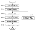
次に、図4のフローチャートに従い、エッジ検出部3100より、注目画素データがエッジ画素であると判定された場合の補正2値化演算部3230の処理内容の説明をする。ここで、注目多値画素の値を図5にしたがい「A」とする。
Next, according to the flowchart of FIG. 4, the processing content of the correction
先ず、入力された多値画像データから、注目画素値Aおよびその周辺画素値を読み込む(ステップS400)。 First, the target pixel value A and its surrounding pixel values are read from the input multi-value image data (step S400).
次に、注目画素の目標値A’を算出する(ステップS401)。 Next, the target value A ′ of the target pixel is calculated (step S401).
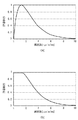
目標値A’は、注目画素Aを中心とする11×11画素領域の画像データと視覚特性フィルタ(サイズは11×11とする)を用いてフィルタリング処理、すなわち、画像データとフィルタの係数の積和を求める。図6(a)は目標値A’を算出するために使用する視覚特性フィルタ(第1のフィルタ)の周波数特性を示したものの一例である。同図は、横軸に周波数、縦軸に人間の目の周波数応答値を示している。 The target value A ′ is a filtering process using image data of an 11 × 11 pixel area centered on the pixel of interest A and a visual characteristic filter (with a size of 11 × 11), that is, the product of the image data and the coefficient of the filter. Find the sum. FIG. 6A shows an example of the frequency characteristic of the visual characteristic filter (first filter) used for calculating the target value A ′. In the figure, the horizontal axis represents the frequency, and the vertical axis represents the frequency response value of the human eye.
次に、注目画素及びその周辺画素を2値化する(ステップS402)。2値化方法は、前述した非エッジ画素を2値化する場合と同様、閾値マトリクス3220を用いて、比較演算することで2値化する。
Next, the pixel of interest and its surrounding pixels are binarized (step S402). In the binarization method, as in the case of binarization of the non-edge pixels described above, binarization is performed by performing a comparison operation using the
次に、周辺画素の出力値B’を算出する(ステップS403)。 Next, the output value B ′ of the surrounding pixels is calculated (step S403).
周辺画素の出力値B’の算出方法は、注目画素を中心とする11×11画素領域の周辺画素の2値化データ(注目画素の2値化データBを含む)と、画像処理装置のエンジン特性および視覚特性の2つの特性をあわせたフィルタの積和を求めることで算出する。ここで、注意する点は、2値化データは、1画素分に相当する4つの領域の各領域毎の“1”の個数を表わすことに注意されたい。図6(b)は、画像処理装置のエンジン特性および視覚特性の2つの特性をあわせたフィルタ(第2のフィルタ)の周波数特性を示した一例である。図6(a)同様、横軸に周波数、縦軸に人間の目の周波数応答値を示している。図示の如く、フィルタの縦軸は、最大値“1”とする実数で示されているので、B’の値は小数点を含む値となる。 The calculation method of the output value B ′ of the peripheral pixel includes the binarized data (including the binarized data B of the target pixel) of the peripheral pixel in the 11 × 11 pixel area centered on the target pixel, and the engine of the image processing apparatus. The calculation is performed by obtaining the product sum of the filters that combine the two characteristics of the characteristics and the visual characteristics. Here, it should be noted that the binarized data represents the number of “1” s in each of four regions corresponding to one pixel. FIG. 6B is an example showing the frequency characteristics of a filter (second filter) that combines two characteristics of the engine characteristics and visual characteristics of the image processing apparatus. Similar to FIG. 6A, the horizontal axis indicates the frequency, and the vertical axis indicates the frequency response value of the human eye. As shown in the figure, the vertical axis of the filter is indicated by a real number having a maximum value “1”, so the value of B ′ is a value including a decimal point.
次に、注目画素の補正量C’を算出する(ステップS404)。補正量C’の算出方法は、以下の式で算出する。
C’=A’−B’
Next, the correction amount C ′ of the target pixel is calculated (step S404). The calculation method of the correction amount C ′ is calculated by the following equation.
C ′ = A′−B ′
次に、注目画素Aの2値化結果Bに、補正量C’を加算した加算結果を着目画素の2値化結果Dとして出力する(S405)。注目画素の2値化結果Dは以下の式で算出する。
D=B+C’
Next, the addition result obtained by adding the correction amount C ′ to the binarization result B of the target pixel A is output as the binarization result D of the target pixel (S405). The binarization result D of the target pixel is calculated by the following formula.
D = B + C ′
ここで、仮に、注目画素の2値化結果Bが、4つの領域中の1つを走査露光するものとして2値化され、補正値C’が“1.1”であったとする。この場合、D=1+1.1=2.1となるが、小数点以下を切り捨て、もしくは四捨五入した結果を、注目画素の出力値Dとして決定する。この場合、注目画素は4つの領域中、2つを露光するものとして決定することになる。 Here, it is assumed that the binarization result B of the target pixel is binarized assuming that one of the four areas is scanned and exposed, and the correction value C ′ is “1.1”. In this case, D = 1 + 1.1 = 2.1, but the result of rounding off or rounding off the decimal point is determined as the output value D of the target pixel. In this case, the target pixel is determined as exposing two of the four regions.
以上の如く、注目画素Aを2値化した値Bに補正量C’を加えることで、目標値A’に近づくため、視覚的にエッジ部のジャギーや途切れが目立ち難くなる。 As described above, by adding the correction amount C ′ to the binarized value B of the pixel of interest A, it approaches the target value A ′, so that jaggies and breaks in the edge portion are not visually noticeable.
最後に、注目画素の出力値を更新する(ステップS406)。多値画像データは主走査、副走査方向に順次入力され、あるバンド領域(第1の実施形態では注目画素周囲の11×11画素)を読み込み、注目画素を1画素単位ずつ処理する。補正2値化演算部3230では、注目画素を中心とする周囲画素11×11の入力値および2値化結果を参照するため、周囲画素内で複数のエッジ画素があると、周囲画素がエッジ画素として処理された場合と、非エッジ画素として処理された場合で値が異なるため、周辺画素の出力値B’を正確に算出することができなくなる。そこで、ステップS406で補正した注目画素の出力値を更新することで、周囲画素11×11に複数のエッジ画素がある場合でもエッジ画素の補正処理を次のエッジ画素の補正処理を正確に行うことができる。
Finally, the output value of the target pixel is updated (step S406). Multi-value image data is sequentially input in the main scanning and sub-scanning directions, reads a certain band region (11 × 11 pixels around the pixel of interest in the first embodiment), and processes the pixel of interest one pixel at a time. The correction
以上のように、注目画素データがエッジ画素であるか、非エッジ画素であるかによって、セレクタ3240において2値化処理内容を切替え、2値画像データを出力する。そして、視覚特性および画像処理装置のエンジン特性を考慮して、エッジ画素の出力値を補正することで、ジャギーや細線の途切れが目立ち難い高画質な出力画像を得ることができる。
As described above, the binarization processing content is switched in the
なお、本実施形態では補正2値化演算部での周囲画素の参照範囲を11×11画素としたが、このサイズに限定されるものではない。 In the present embodiment, the reference range of the surrounding pixels in the correction binarization calculation unit is 11 × 11 pixels. However, the size is not limited to this size.
<第2の実施形態>
上記第1の実施形態では、中間調の画像データにスクリーン処理を施し、2値化する画像処理方法および装置において、注目画素がエッジ画素であるか、非エッジ画素であるかによって、2値化処理内容を切替え、2値画像データを出力することとした。具体的には、注目画素が非エッジ画素の場合は、スクリーン処理により2値化を行う。一方、注目画素がエッジ画素の場合は、前述した補正2値化演算部で、エッジ補正処理を行うことで2値化を行った。
<Second Embodiment>
In the first embodiment, in the image processing method and apparatus for performing binarization by performing screen processing on halftone image data, binarization is performed depending on whether the pixel of interest is an edge pixel or a non-edge pixel. The processing content is switched and binary image data is output. Specifically, when the target pixel is a non-edge pixel, binarization is performed by screen processing. On the other hand, when the target pixel is an edge pixel, binarization is performed by performing edge correction processing in the above-described correction binarization calculation unit.
しかし、補正2値化演算部でのエッジ補正処理では、補正後の出力値を参照するため、出力値を記憶するメモリが必要である。ハードウェア構成を実現しようとすると、より少ないメモリ容量となる。また、スクリーン処理を施した画像データのエッジ部に発生するジャギーや細線の途切れを防止する必要もある。 However, in the edge correction processing in the correction binarization calculation unit, a memory for storing the output value is required to refer to the output value after correction. An attempt to implement a hardware configuration results in a smaller memory capacity. It is also necessary to prevent jaggies and fine lines from being interrupted at the edge of the image data subjected to the screen processing.
そこで、本第2の実施形態では、中間調の画像データにスクリーン処理を施した画像データのエッジに発生するジャギーや細線の途切れを防止しつつ、より少ないメモリ容量で、ハードウェア構成を実現するものについて説明する。 Therefore, in the second embodiment, a hardware configuration is realized with a smaller memory capacity while preventing jaggies and fine lines from being interrupted at the edges of image data obtained by performing screen processing on halftone image data. I will explain things.
図7は、前述した画像処理装置における本第2の実施形態の特徴である2値化処理の一手法を示す構成図である。 FIG. 7 is a configuration diagram showing one method of binarization processing that is a feature of the second embodiment in the above-described image processing apparatus.
なお、図7の構成において、第1の実施形態の図2と同一の構成要素については、同一の符号を付加し、その詳細については説明を省略する。 In the configuration of FIG. 7, the same components as those in FIG. 2 of the first embodiment are denoted by the same reference numerals, and description thereof is omitted.
図7において、図2と異なる点は、セレクタ3240で出力する2値画像データを補正2値化演算部3230にフィードバックする系統を取り除いた点と、後述で説明する細線検出部6300およびPWM処理部6250を追加した点である。
7 differs from FIG. 2 in that the system for feeding back the binary image data output from the
つまり、前述した出力結果である2値画像データをフィードバックする系統を取り除くことで、出力値を記憶するメモリが不要となり、より少ないメモリでハードウェア構成が実現できる。また、エッジ検出部および細線検出部の結果に応じて、2値化処理内容を切替えることで、スクリーン処理を施した画像データのエッジ部に発生するジャギーや細線の途切れを防止することができる。 That is, by removing the system for feeding back the binary image data as the output result described above, a memory for storing output values becomes unnecessary, and a hardware configuration can be realized with less memory. Further, by switching the contents of the binarization process according to the results of the edge detection unit and the thin line detection unit, it is possible to prevent jaggies and fine lines from being interrupted at the edge of the image data subjected to the screen processing.
以下、第2の実施形態の詳細な説明をする。 Hereinafter, the second embodiment will be described in detail.
PWM処理部6250は、入力された注目画素データに対して、周囲画素を参照せず、単純に注目画素の値から2値画像データ(1×4ビット)を出力する。
The
PWM変換方法は、入力された多値のデジタルデータをD/A変換によって一旦電圧変動信号に変換する。そして、この変換信号の電圧レベルと入力データの入力周期と同じ周期の参照波の電圧レベルとを比較し、変換信号が大きけれ発光素子をオン、小さければ発光素子をオフとする方法である。この方法によれば、比較対照の参照波を画像処理制御信号に応じて切替えることで、画素の主走査方向の大きさおよびドット形成位置を制御することができる。 In the PWM conversion method, input multi-value digital data is once converted into a voltage fluctuation signal by D / A conversion. Then, the voltage level of the conversion signal is compared with the voltage level of the reference wave having the same period as the input period of the input data, and the light emitting element is turned on when the conversion signal is large and the light emitting element is small. According to this method, the size of the pixel in the main scanning direction and the dot formation position can be controlled by switching the reference wave for comparison in accordance with the image processing control signal.
図8は、PWM処理による具体的な入力画像と出力画像の関係を示した一例である。図示では、1ドットで表わす領域を4分割することで、濃度を0乃至4の5段階で表わす例を示している。 FIG. 8 is an example showing a specific relationship between an input image and an output image by PWM processing. In the figure, an example is shown in which the density is expressed in five levels from 0 to 4 by dividing the area represented by one dot into four.
細線検出部6300は、入力された多値画像データが細線かどうかを検出する。ここでいう細線とは、線の幅が2ドットの幅以下で構成されるような細い線画像データのことである。
The fine
図9(a)、(b)は細線検出部6300で使用する線形フィルタの一例である。第1の実施形態のエッジ検出部3100と同様、入力された多値画像データと線形フィルタの積和を算出する。その算出値と細線判定閾値を比較することで、細線画素あるいは非細線画素かを判定する。なお、図9(a)は垂直方向の細線検出フィルタを示し、同図(b)は水平方向の細線検出フィルタを示している。
FIGS. 9A and 9B are examples of linear filters used in the thin
なお、本第2の実施形態では細線検出方法として、図9(a),(b)に示した線形フィルタの2種類を示したが、他の方法で細線検出を行っても良い。また、細線判定において、入力画像データと線形フィルタの積和結果を正規化しても良い。また、細線判定閾値は、固定値だけでなく、LUTデータとして持ち、注目画素データに応じて可変の値に設定しても良いし、関数として定義しても良い。 In the second embodiment, two types of linear filters shown in FIGS. 9A and 9B are shown as thin line detection methods. However, thin line detection may be performed by other methods. In addition, in the thin line determination, the product-sum result of the input image data and the linear filter may be normalized. Further, the thin line determination threshold is not only a fixed value but also LUT data, and may be set to a variable value according to the target pixel data, or may be defined as a function.
以下、図7における処理の流れを説明する。 Hereinafter, the flow of processing in FIG. 7 will be described.
まず、エッジ検出部3100において、入力された多値画像データの注目画素がエッジ画素あるいは非エッジ画素かを判定する。
First, the
次に、細線検出部6300において、入力された多値画像データの注目画素が細線画素あるいは非細線画素かを判定する。
Next, the thin
すなわち、本第2の本実施形態では、エッジ検出結果と細線検出結果に応じて、注目画素の2値化処理を切替える。つまり、注目画素が非エッジ画素かつ非細線画素の場合は、スクリーン処理部3210にて2値化処理を行う。注目画素がエッジ画素かつ非細線画素の場合は、補正2値化演算部3230にて2値化処理を行う。更に、注目画素がエッジ画素且つ細線画素の場合は、PWM処理部6250にて2値化処理を行う。
That is, in the second embodiment, the binarization process for the target pixel is switched according to the edge detection result and the thin line detection result. That is, when the target pixel is a non-edge pixel and a non-thin line pixel, the
図10は、エッジ判定結果および細線判定結果に対応する2値化の処理内容をまとめた表を示す。 FIG. 10 shows a table summarizing the binarization processing contents corresponding to the edge determination result and the thin line determination result.
図15は、本第1実施形態および本第2の実施形態で出力された2値画像データを示している。画像のエッジ部が補正されている。 FIG. 15 shows binary image data output in the first embodiment and the second embodiment. The edge of the image is corrected.
このように、エッジ検出部および細線検出部の結果に応じて、2値化処理内容を切替えることで、スクリーン処理を施した画像データのエッジ部に発生するジャギーや細線の途切れを防止することができる。また、第1の実施形態で使用していた出力結果である2値画像データをフィードバックする系統を取り除くことで、出力値を記憶するメモリが不要となり、より少ないメモリでハードウェア構成が実現できる。 In this way, by switching the contents of the binarization process according to the results of the edge detection unit and the fine line detection unit, it is possible to prevent the jaggy and the fine line from being interrupted at the edge part of the image data subjected to the screen process. it can. Further, by removing the system for feeding back the binary image data, which is the output result used in the first embodiment, a memory for storing output values becomes unnecessary, and a hardware configuration can be realized with less memory.
なお、本第2の実施形態では注目画素が細線画素の場合は、PWM処理を行うことで2値化データを生成していたが、高線数のスクリーンを用いたスクリーン処理を行って2値化データを生成しても、同等の結果を得ることができる。 In the second embodiment, when the pixel of interest is a thin line pixel, binarized data is generated by performing PWM processing. However, binary processing is performed by performing screen processing using a screen with a high line number. Even if generated data is generated, an equivalent result can be obtained.
Claims (5)
前記入力画像データに対してスクリーン処理を施すスクリーン処理手段と、
前記入力画像データに対して、視覚特性を有する第1のフィルタを用いてフィルタ処理する第1のフィルタ処理手段と、
前記エッジ検出手段によって前記入力画像データの注目画素がエッジであると検出された場合、該注目画素に対応する前記第1のフィルタ処理手段による結果に応じて、該注目画素の前記スクリーン処理手段による結果を補正し、該注目画素の出力値を決定する補正手段と
を備えることを特徴とする画像処理装置。 Edge detecting means for detecting an edge portion of input image data ;
Screen processing means for performing screen processing on the input image data ;
First filter processing means for filtering the input image data using a first filter having visual characteristics;
When the target pixel of the input image data is detected to be an edge by the edge detection unit, the screen processing unit of the target pixel is determined according to the result of the first filter processing unit corresponding to the target pixel. An image processing apparatus comprising: correction means for correcting a result and determining an output value of the target pixel .
前記入力画像データの細線を検出する細線検出手段と、Fine line detecting means for detecting a thin line of the input image data;
前記入力画像データに対してスクリーン処理を施すスクリーン処理手段と、Screen processing means for performing screen processing on the input image data;
前記入力画像データに対して、視覚特性を有する第2のフィルタを用いてフィルタ処理する第2のフィルタ処理手段と、Second filter processing means for filtering the input image data using a second filter having visual characteristics;
前記エッジ検出手段によって前記入力画像データの注目画素がエッジであることが検出され、かつ前記細線検出手段によって該注目画素が非細線であると検出された場合、該注目画素に対応する前記第2のフィルタ処理手段による処理結果に応じて、前記注目画素の前記スクリーン処理手段による結果を補正する補正手段と、When the edge detection unit detects that the pixel of interest of the input image data is an edge and the thin line detection unit detects that the pixel of interest is a non-thin line, the second pixel corresponding to the pixel of interest A correction unit that corrects a result of the screen processing unit for the target pixel according to a processing result of the filter processing unit.
前記細線検出手段によって前記注目画素が細線の画素であると検出された場合、前記注目画素をPWM変換するPWM変換手段とPWM conversion means for PWM-converting the target pixel when the target pixel is detected as a thin line pixel by the thin line detection unit;
を備えることを特徴とする画像処理装置。An image processing apparatus comprising:
入力画像データのエッジ部を検出するエッジ検出工程と、
前記入力画像データに対してスクリーン処理を施すスクリーン処理工程と、
前記入力画像データに対して、視覚特性を有する第1のフィルタを用いてフィルタ処理する第1のフィルタ処理工程と、
前記エッジ検出工程によって前記入力画像データの注目画素がエッジであることが検出された場合、該注目画素に対応する前記第1のフィルタ処理工程による結果に応じて該注目画素の前記スクリーン処理工程による結果を補正し、該注目画素の出力値を決定する補正工程と
を有することを特徴とする画像処理装置の制御方法。 A method for controlling an image picture processor,
An edge detection step for detecting an edge portion of the input image data ;
A screen processing step of performing screen processing on the input image data ;
A first filtering process for filtering the input image data using a first filter having visual characteristics;
When it is detected by the edge detection step that the pixel of interest of the input image data is an edge, the screen processing step of the pixel of interest is performed according to the result of the first filter processing step corresponding to the pixel of interest. A correction step of correcting the result and determining the output value of the target pixel;
A control method for an image processing apparatus, comprising:
入力画像データのエッジ部を検出するエッジ検出工程と、An edge detection step for detecting an edge portion of the input image data;
前記入力画像データの細線の細線を検出する細線検出工程と、A fine line detecting step of detecting a fine line of the input image data;
前記入力画像データに対してスクリーン処理を施すスクリーン処理工程と、A screen processing step of performing screen processing on the input image data;
前記入力画像データに対して、視覚特性を有する第2のフィルタを用いてフィルタ処理する第2のフィルタ処理工程と、A second filtering process for filtering the input image data using a second filter having visual characteristics;
前記エッジ検出工程によって前記入力画像データの注目画素がエッジであることが検出され、かつ前記細線検出工程によって該注目画素が非細線であると検出された場合、該注目画素に対応する前記第2のフィルタ処理工程による処理結果に応じて、前記注目画素の前記スクリーン処理工程による結果を補正する補正工程と、When it is detected that the target pixel of the input image data is an edge by the edge detection step and the target pixel is detected to be a non-thin line by the thin line detection step, the second corresponding to the target pixel A correction step of correcting the result of the screen processing step for the pixel of interest according to the processing result of the filtering processing step,
前記細線検出工程によって前記注目画素が細線の画素であると検出された場合、前記注目画素の入力画像データをPWM変換するPWM変換工程とA PWM conversion step of performing PWM conversion on input image data of the target pixel when the target pixel is detected as a thin line pixel by the thin line detection step;
を有することを特徴とする画像処理装置の制御方法。A control method for an image processing apparatus, comprising:
Priority Applications (3)
| Application Number | Priority Date | Filing Date | Title |
|---|---|---|---|
| JP2007269528A JP4912270B2 (en) | 2007-10-16 | 2007-10-16 | Image processing apparatus and control method thereof |
| US12/236,185 US8687240B2 (en) | 2007-10-16 | 2008-09-23 | Image processing apparatus and control method for performing screen processing |
| US14/177,400 US9361557B2 (en) | 2007-10-16 | 2014-02-11 | Image processing apparatus and control method for performing screen processing |
Applications Claiming Priority (1)
| Application Number | Priority Date | Filing Date | Title |
|---|---|---|---|
| JP2007269528A JP4912270B2 (en) | 2007-10-16 | 2007-10-16 | Image processing apparatus and control method thereof |
Related Child Applications (1)
| Application Number | Title | Priority Date | Filing Date |
|---|---|---|---|
| JP2010201334A Division JP4861506B2 (en) | 2010-09-08 | 2010-09-08 | Image processing apparatus and control method thereof |
Publications (3)
| Publication Number | Publication Date |
|---|---|
| JP2009100228A JP2009100228A (en) | 2009-05-07 |
| JP2009100228A5 JP2009100228A5 (en) | 2010-10-21 |
| JP4912270B2 true JP4912270B2 (en) | 2012-04-11 |
Family
ID=40534281
Family Applications (1)
| Application Number | Title | Priority Date | Filing Date |
|---|---|---|---|
| JP2007269528A Expired - Fee Related JP4912270B2 (en) | 2007-10-16 | 2007-10-16 | Image processing apparatus and control method thereof |
Country Status (2)
| Country | Link |
|---|---|
| US (2) | US8687240B2 (en) |
| JP (1) | JP4912270B2 (en) |
Families Citing this family (18)
| Publication number | Priority date | Publication date | Assignee | Title |
|---|---|---|---|---|
| US8154617B2 (en) * | 2009-09-30 | 2012-04-10 | Sony Corporation | Method of detecting the existence of visually sensitive thin lines in a digital image |
| JP5534787B2 (en) * | 2009-11-24 | 2014-07-02 | キヤノン株式会社 | Image processing apparatus and image processing method |
| JP5675253B2 (en) * | 2009-12-28 | 2015-02-25 | キヤノン株式会社 | Image processing apparatus, image processing method, and computer program |
| JP5709479B2 (en) * | 2010-11-19 | 2015-04-30 | キヤノン株式会社 | Image processing apparatus and image processing method |
| JP5747570B2 (en) | 2011-03-07 | 2015-07-15 | セイコーエプソン株式会社 | Printing apparatus and printing method |
| US8842938B2 (en) * | 2012-06-27 | 2014-09-23 | Xerox Corporation | Method and system for performing resolution expansion with high quality edge enhancement |
| KR101996917B1 (en) * | 2012-07-20 | 2019-10-02 | 삼성디스플레이 주식회사 | Method and apparatus for inspecting flat panel display |
| JP5566500B2 (en) * | 2013-05-07 | 2014-08-06 | キヤノン株式会社 | Resolution conversion apparatus and control method thereof |
| US9749496B2 (en) * | 2013-06-19 | 2017-08-29 | Canon Kabushiki Kaisha | Performing halftone processing using intra-cell sum value differences applied so as to correct boundary pixels |
| JP6234888B2 (en) * | 2014-06-26 | 2017-11-22 | 京セラドキュメントソリューションズ株式会社 | Image forming apparatus |
| JP6403490B2 (en) * | 2014-08-20 | 2018-10-10 | キヤノン株式会社 | Image processing apparatus, image forming apparatus, image processing method, and program. |
| JP6541320B2 (en) * | 2014-09-24 | 2019-07-10 | キヤノン株式会社 | Image processing apparatus, image processing method, computer program |
| US9681022B2 (en) * | 2014-12-25 | 2017-06-13 | Ricoh Company, Ltd. | Image processing apparatus, image processing method, and recording medium |
| JP6452504B2 (en) * | 2015-03-10 | 2019-01-16 | キヤノン株式会社 | Image forming apparatus, image forming method, and program |
| JP6550816B2 (en) * | 2015-03-18 | 2019-07-31 | 株式会社リコー | INFORMATION PROCESSING APPARATUS, IMAGE FORMING APPARATUS, IMAGE PROCESSING METHOD, AND PROGRAM |
| JP6649750B2 (en) * | 2015-11-16 | 2020-02-19 | キヤノン株式会社 | Image processing apparatus and image processing method |
| JP2017181983A (en) * | 2016-03-31 | 2017-10-05 | 株式会社ジャパンディスプレイ | Display device |
| JP6824052B2 (en) * | 2017-01-25 | 2021-02-03 | キヤノン株式会社 | Image processing device, its control method, and program |
Family Cites Families (25)
| Publication number | Priority date | Publication date | Assignee | Title |
|---|---|---|---|---|
| US5029227A (en) * | 1985-08-30 | 1991-07-02 | Canon Kabushiki Kaisha | Image processing apparatus |
| JP2589295B2 (en) * | 1986-11-14 | 1997-03-12 | キヤノン株式会社 | Image forming device |
| EP0500375B1 (en) * | 1991-02-22 | 1998-07-08 | Canon Kabushiki Kaisha | Image modification system |
| JP3219421B2 (en) | 1991-05-17 | 2001-10-15 | キヤノン株式会社 | Information recording device |
| US5268774A (en) * | 1991-11-27 | 1993-12-07 | Xerox Corporation | Halftoning with enhanced dynamic range and edge enhanced error diffusion |
| JP3310744B2 (en) * | 1993-12-22 | 2002-08-05 | 東芝テック株式会社 | Resolution converter |
| JP2973899B2 (en) * | 1995-11-17 | 1999-11-08 | 富士ゼロックス株式会社 | Image processing device |
| JPH09247450A (en) * | 1996-03-13 | 1997-09-19 | Sharp Corp | Image processing unit |
| JPH09321986A (en) | 1996-05-28 | 1997-12-12 | Ricoh Co Ltd | Adaptive gradation processor |
| JP3644183B2 (en) * | 1997-03-17 | 2005-04-27 | 富士ゼロックス株式会社 | Image processing device |
| JP3784537B2 (en) * | 1998-06-09 | 2006-06-14 | 株式会社リコー | Image processing device |
| JP3823562B2 (en) * | 1998-10-02 | 2006-09-20 | コニカミノルタビジネステクノロジーズ株式会社 | Image processing device |
| JP3767878B2 (en) * | 1998-10-26 | 2006-04-19 | 株式会社リコー | Image processing apparatus with output correction inside character |
| JP3962890B2 (en) * | 1999-03-05 | 2007-08-22 | セイコーエプソン株式会社 | Image data modifying apparatus, image data modifying method, and computer readable recording medium recording image data modifying program |
| US7224488B2 (en) * | 2001-06-12 | 2007-05-29 | Fujifilm Corporation | Method of correcting threshold array, dot pattern data structure, method of correcting pixel layout of image, and method of determining threshold array for generating image |
| JP2003230010A (en) * | 2001-11-30 | 2003-08-15 | Ricoh Co Ltd | Image processing apparatus and image processing method |
| EP1331804A3 (en) * | 2002-01-24 | 2003-11-19 | Ricoh Company, Ltd. | Image forming device, image forming method, computer program, and recording medium |
| JP2003234893A (en) * | 2002-02-06 | 2003-08-22 | Ricoh Co Ltd | Image processor |
| US7139101B2 (en) * | 2002-10-31 | 2006-11-21 | Xerox Corporation | Anisotropic stochastic screen |
| KR100524072B1 (en) * | 2003-06-28 | 2005-10-26 | 삼성전자주식회사 | Method for improving image quality |
| US8049933B2 (en) * | 2003-09-17 | 2011-11-01 | Canon Kabushiki Kaisha | Copy-forgery-inhibited pattern image generation method and image processing apparatus |
| JP4243854B2 (en) * | 2004-06-08 | 2009-03-25 | 富士ゼロックス株式会社 | Image processing apparatus, image processing method, image processing program, and storage medium |
| US7602976B2 (en) * | 2006-02-17 | 2009-10-13 | Sony Corporation | Compressible earth mover's distance |
| JP2007235430A (en) * | 2006-02-28 | 2007-09-13 | Ricoh Co Ltd | Image processor and processing method, image distribution device, image formation apparatus, program, and recording medium |
| JP4600352B2 (en) * | 2006-05-25 | 2010-12-15 | 富士ゼロックス株式会社 | Image processing apparatus, image forming apparatus, and image processing method |
-
2007
- 2007-10-16 JP JP2007269528A patent/JP4912270B2/en not_active Expired - Fee Related
-
2008
- 2008-09-23 US US12/236,185 patent/US8687240B2/en not_active Expired - Fee Related
-
2014
- 2014-02-11 US US14/177,400 patent/US9361557B2/en active Active
Also Published As
| Publication number | Publication date |
|---|---|
| US8687240B2 (en) | 2014-04-01 |
| US20140160533A1 (en) | 2014-06-12 |
| US9361557B2 (en) | 2016-06-07 |
| JP2009100228A (en) | 2009-05-07 |
| US20090097776A1 (en) | 2009-04-16 |
Similar Documents
| Publication | Publication Date | Title |
|---|---|---|
| JP4912270B2 (en) | Image processing apparatus and control method thereof | |
| US9734439B2 (en) | Image processing apparatus and method thereof | |
| EP1505821B1 (en) | Image processing apparatus, an image forming apparatus and an image processing method | |
| JP3472479B2 (en) | Image processing device | |
| KR101800931B1 (en) | Image processing apparatus, image processing method, and computer program | |
| US7889395B2 (en) | Image processing apparatus, image processing method, and program | |
| US10999473B2 (en) | Image processing apparatus, image processing method, and recording medium to correct characteristic amount of target pixel using brightness at two pixels in set target area | |
| JP6338469B2 (en) | Image processing apparatus and image processing method | |
| JP4402090B2 (en) | Image forming apparatus, image forming method, program, and recording medium | |
| WO2000024189A1 (en) | Printing apparatus and method | |
| EP0500174A1 (en) | Image processing method and scan/print system for performing the method | |
| US20120026554A1 (en) | Image processing apparatus | |
| JP4861506B2 (en) | Image processing apparatus and control method thereof | |
| US7502512B2 (en) | Image processing apparatus and image processing method | |
| JP5316312B2 (en) | Image processing device | |
| JP4740913B2 (en) | Image processing apparatus, image processing method, image forming apparatus and program, and recording medium | |
| JP4545167B2 (en) | Image processing method, image processing apparatus, image forming apparatus, computer program, and recording medium | |
| JP4080252B2 (en) | Image processing apparatus, image forming apparatus, image processing method, program, and recording medium | |
| JP2006340144A (en) | Image processing device | |
| JP2006011754A (en) | Image processing device and image processing method | |
| JP4137067B2 (en) | Image processing method and apparatus | |
| JP4545134B2 (en) | Image processing method, image processing apparatus, image forming apparatus, computer program, and recording medium | |
| JP2006049992A (en) | Image processor | |
| JP2009134583A (en) | Image forming apparatus, image forming method, computer program and recording medium | |
| KR20080000945A (en) | Image processing method for outputting a scanning image with enhanced quality |
Legal Events
| Date | Code | Title | Description |
|---|---|---|---|
| A521 | Request for written amendment filed |
Free format text: JAPANESE INTERMEDIATE CODE: A523 Effective date: 20100908 |
|
| A621 | Written request for application examination |
Free format text: JAPANESE INTERMEDIATE CODE: A621 Effective date: 20100908 |
|
| A977 | Report on retrieval |
Free format text: JAPANESE INTERMEDIATE CODE: A971007 Effective date: 20111215 |
|
| TRDD | Decision of grant or rejection written | ||
| A01 | Written decision to grant a patent or to grant a registration (utility model) |
Free format text: JAPANESE INTERMEDIATE CODE: A01 Effective date: 20111219 |
|
| A01 | Written decision to grant a patent or to grant a registration (utility model) |
Free format text: JAPANESE INTERMEDIATE CODE: A01 |
|
| A61 | First payment of annual fees (during grant procedure) |
Free format text: JAPANESE INTERMEDIATE CODE: A61 Effective date: 20120117 |
|
| R151 | Written notification of patent or utility model registration |
Ref document number: 4912270 Country of ref document: JP Free format text: JAPANESE INTERMEDIATE CODE: R151 |
|
| FPAY | Renewal fee payment (event date is renewal date of database) |
Free format text: PAYMENT UNTIL: 20150127 Year of fee payment: 3 |
|
| LAPS | Cancellation because of no payment of annual fees |