JP4902044B2 - Semiconductor laser device, optical transmission device, optical transmission system, electronic device, control device, connection connector, communication device, optical transmission method, and data transmission / reception method - Google Patents
Semiconductor laser device, optical transmission device, optical transmission system, electronic device, control device, connection connector, communication device, optical transmission method, and data transmission / reception method Download PDFInfo
- Publication number
- JP4902044B2 JP4902044B2 JP2000284426A JP2000284426A JP4902044B2 JP 4902044 B2 JP4902044 B2 JP 4902044B2 JP 2000284426 A JP2000284426 A JP 2000284426A JP 2000284426 A JP2000284426 A JP 2000284426A JP 4902044 B2 JP4902044 B2 JP 4902044B2
- Authority
- JP
- Japan
- Prior art keywords
- semiconductor laser
- light
- wavelength
- transmission
- light receiving
- Prior art date
- Legal status (The legal status is an assumption and is not a legal conclusion. Google has not performed a legal analysis and makes no representation as to the accuracy of the status listed.)
- Expired - Lifetime
Links
Images


Classifications
-
- H—ELECTRICITY
- H01—ELECTRIC ELEMENTS
- H01S—DEVICES USING THE PROCESS OF LIGHT AMPLIFICATION BY STIMULATED EMISSION OF RADIATION [LASER] TO AMPLIFY OR GENERATE LIGHT; DEVICES USING STIMULATED EMISSION OF ELECTROMAGNETIC RADIATION IN WAVE RANGES OTHER THAN OPTICAL
- H01S5/00—Semiconductor lasers
- H01S5/02—Structural details or components not essential to laser action
- H01S5/022—Mountings; Housings
- H01S5/02208—Mountings; Housings characterised by the shape of the housings
- H01S5/02212—Can-type, e.g. TO-CAN housings with emission along or parallel to symmetry axis
-
- H—ELECTRICITY
- H01—ELECTRIC ELEMENTS
- H01L—SEMICONDUCTOR DEVICES NOT COVERED BY CLASS H10
- H01L2224/00—Indexing scheme for arrangements for connecting or disconnecting semiconductor or solid-state bodies and methods related thereto as covered by H01L24/00
- H01L2224/01—Means for bonding being attached to, or being formed on, the surface to be connected, e.g. chip-to-package, die-attach, "first-level" interconnects; Manufacturing methods related thereto
- H01L2224/42—Wire connectors; Manufacturing methods related thereto
- H01L2224/47—Structure, shape, material or disposition of the wire connectors after the connecting process
- H01L2224/48—Structure, shape, material or disposition of the wire connectors after the connecting process of an individual wire connector
- H01L2224/4805—Shape
- H01L2224/4809—Loop shape
- H01L2224/48091—Arched
-
- H—ELECTRICITY
- H01—ELECTRIC ELEMENTS
- H01L—SEMICONDUCTOR DEVICES NOT COVERED BY CLASS H10
- H01L2224/00—Indexing scheme for arrangements for connecting or disconnecting semiconductor or solid-state bodies and methods related thereto as covered by H01L24/00
- H01L2224/01—Means for bonding being attached to, or being formed on, the surface to be connected, e.g. chip-to-package, die-attach, "first-level" interconnects; Manufacturing methods related thereto
- H01L2224/42—Wire connectors; Manufacturing methods related thereto
- H01L2224/47—Structure, shape, material or disposition of the wire connectors after the connecting process
- H01L2224/48—Structure, shape, material or disposition of the wire connectors after the connecting process of an individual wire connector
- H01L2224/481—Disposition
- H01L2224/48151—Connecting between a semiconductor or solid-state body and an item not being a semiconductor or solid-state body, e.g. chip-to-substrate, chip-to-passive
- H01L2224/48221—Connecting between a semiconductor or solid-state body and an item not being a semiconductor or solid-state body, e.g. chip-to-substrate, chip-to-passive the body and the item being stacked
- H01L2224/48245—Connecting between a semiconductor or solid-state body and an item not being a semiconductor or solid-state body, e.g. chip-to-substrate, chip-to-passive the body and the item being stacked the item being metallic
- H01L2224/48247—Connecting between a semiconductor or solid-state body and an item not being a semiconductor or solid-state body, e.g. chip-to-substrate, chip-to-passive the body and the item being stacked the item being metallic connecting the wire to a bond pad of the item
-
- H—ELECTRICITY
- H01—ELECTRIC ELEMENTS
- H01L—SEMICONDUCTOR DEVICES NOT COVERED BY CLASS H10
- H01L2224/00—Indexing scheme for arrangements for connecting or disconnecting semiconductor or solid-state bodies and methods related thereto as covered by H01L24/00
- H01L2224/01—Means for bonding being attached to, or being formed on, the surface to be connected, e.g. chip-to-package, die-attach, "first-level" interconnects; Manufacturing methods related thereto
- H01L2224/42—Wire connectors; Manufacturing methods related thereto
- H01L2224/47—Structure, shape, material or disposition of the wire connectors after the connecting process
- H01L2224/49—Structure, shape, material or disposition of the wire connectors after the connecting process of a plurality of wire connectors
- H01L2224/491—Disposition
- H01L2224/4911—Disposition the connectors being bonded to at least one common bonding area, e.g. daisy chain
- H01L2224/49113—Disposition the connectors being bonded to at least one common bonding area, e.g. daisy chain the connectors connecting different bonding areas on the semiconductor or solid-state body to a common bonding area outside the body, e.g. converging wires
-
- H—ELECTRICITY
- H01—ELECTRIC ELEMENTS
- H01L—SEMICONDUCTOR DEVICES NOT COVERED BY CLASS H10
- H01L33/00—Semiconductor devices with at least one potential-jump barrier or surface barrier specially adapted for light emission; Processes or apparatus specially adapted for the manufacture or treatment thereof or of parts thereof; Details thereof
- H01L33/48—Semiconductor devices with at least one potential-jump barrier or surface barrier specially adapted for light emission; Processes or apparatus specially adapted for the manufacture or treatment thereof or of parts thereof; Details thereof characterised by the semiconductor body packages
- H01L33/58—Optical field-shaping elements
-
- H—ELECTRICITY
- H01—ELECTRIC ELEMENTS
- H01S—DEVICES USING THE PROCESS OF LIGHT AMPLIFICATION BY STIMULATED EMISSION OF RADIATION [LASER] TO AMPLIFY OR GENERATE LIGHT; DEVICES USING STIMULATED EMISSION OF ELECTROMAGNETIC RADIATION IN WAVE RANGES OTHER THAN OPTICAL
- H01S5/00—Semiconductor lasers
- H01S5/005—Optical components external to the laser cavity, specially adapted therefor, e.g. for homogenisation or merging of the beams or for manipulating laser pulses, e.g. pulse shaping
-
- H—ELECTRICITY
- H01—ELECTRIC ELEMENTS
- H01S—DEVICES USING THE PROCESS OF LIGHT AMPLIFICATION BY STIMULATED EMISSION OF RADIATION [LASER] TO AMPLIFY OR GENERATE LIGHT; DEVICES USING STIMULATED EMISSION OF ELECTROMAGNETIC RADIATION IN WAVE RANGES OTHER THAN OPTICAL
- H01S5/00—Semiconductor lasers
- H01S5/02—Structural details or components not essential to laser action
- H01S5/022—Mountings; Housings
- H01S5/02218—Material of the housings; Filling of the housings
- H01S5/0222—Gas-filled housings
-
- H—ELECTRICITY
- H01—ELECTRIC ELEMENTS
- H01S—DEVICES USING THE PROCESS OF LIGHT AMPLIFICATION BY STIMULATED EMISSION OF RADIATION [LASER] TO AMPLIFY OR GENERATE LIGHT; DEVICES USING STIMULATED EMISSION OF ELECTROMAGNETIC RADIATION IN WAVE RANGES OTHER THAN OPTICAL
- H01S5/00—Semiconductor lasers
- H01S5/02—Structural details or components not essential to laser action
- H01S5/022—Mountings; Housings
- H01S5/02218—Material of the housings; Filling of the housings
- H01S5/02232—Liquid-filled housings
-
- H—ELECTRICITY
- H01—ELECTRIC ELEMENTS
- H01S—DEVICES USING THE PROCESS OF LIGHT AMPLIFICATION BY STIMULATED EMISSION OF RADIATION [LASER] TO AMPLIFY OR GENERATE LIGHT; DEVICES USING STIMULATED EMISSION OF ELECTROMAGNETIC RADIATION IN WAVE RANGES OTHER THAN OPTICAL
- H01S5/00—Semiconductor lasers
- H01S5/02—Structural details or components not essential to laser action
- H01S5/022—Mountings; Housings
- H01S5/02218—Material of the housings; Filling of the housings
- H01S5/02234—Resin-filled housings; the housings being made of resin
-
- H—ELECTRICITY
- H01—ELECTRIC ELEMENTS
- H01S—DEVICES USING THE PROCESS OF LIGHT AMPLIFICATION BY STIMULATED EMISSION OF RADIATION [LASER] TO AMPLIFY OR GENERATE LIGHT; DEVICES USING STIMULATED EMISSION OF ELECTROMAGNETIC RADIATION IN WAVE RANGES OTHER THAN OPTICAL
- H01S5/00—Semiconductor lasers
- H01S5/02—Structural details or components not essential to laser action
- H01S5/022—Mountings; Housings
- H01S5/0225—Out-coupling of light
- H01S5/02251—Out-coupling of light using optical fibres
-
- H—ELECTRICITY
- H01—ELECTRIC ELEMENTS
- H01S—DEVICES USING THE PROCESS OF LIGHT AMPLIFICATION BY STIMULATED EMISSION OF RADIATION [LASER] TO AMPLIFY OR GENERATE LIGHT; DEVICES USING STIMULATED EMISSION OF ELECTROMAGNETIC RADIATION IN WAVE RANGES OTHER THAN OPTICAL
- H01S5/00—Semiconductor lasers
- H01S5/02—Structural details or components not essential to laser action
- H01S5/022—Mountings; Housings
- H01S5/0225—Out-coupling of light
- H01S5/02253—Out-coupling of light using lenses
-
- H—ELECTRICITY
- H01—ELECTRIC ELEMENTS
- H01S—DEVICES USING THE PROCESS OF LIGHT AMPLIFICATION BY STIMULATED EMISSION OF RADIATION [LASER] TO AMPLIFY OR GENERATE LIGHT; DEVICES USING STIMULATED EMISSION OF ELECTROMAGNETIC RADIATION IN WAVE RANGES OTHER THAN OPTICAL
- H01S5/00—Semiconductor lasers
- H01S5/02—Structural details or components not essential to laser action
- H01S5/024—Arrangements for thermal management
-
- H—ELECTRICITY
- H01—ELECTRIC ELEMENTS
- H01S—DEVICES USING THE PROCESS OF LIGHT AMPLIFICATION BY STIMULATED EMISSION OF RADIATION [LASER] TO AMPLIFY OR GENERATE LIGHT; DEVICES USING STIMULATED EMISSION OF ELECTROMAGNETIC RADIATION IN WAVE RANGES OTHER THAN OPTICAL
- H01S5/00—Semiconductor lasers
- H01S5/40—Arrangement of two or more semiconductor lasers, not provided for in groups H01S5/02 - H01S5/30
- H01S5/4025—Array arrangements, e.g. constituted by discrete laser diodes or laser bar
- H01S5/4087—Array arrangements, e.g. constituted by discrete laser diodes or laser bar emitting more than one wavelength
Description
【0001】
【発明の属する技術分野】
本発明は、無線通信やセンサー用光源等、空間にその光が放射されて人が直接光源を見るような用途に用いられ、目に対する安全性を確保した半導体レーザ装置、光伝送装置、光伝送システム、パーソナルコンピュータ、携帯情報端末やデジタルカメラ等の空間光伝送システムを利用する電子機器、制御装置および通信装置並びに空間光伝送方法、データ送受信方法に関する。また、本発明は、発光スポットを拡大した半導体レーザ装置、同時送受信可能な光伝送装置、光伝送システム、多チャンネルCATV用やAV用等のファイバ系光伝送システムを利用する電子機器、ファイバ系光伝送システム、制御装置および通信装置並びにファイバ系光伝送方法、データ送受信方法に関する。
【0002】
【従来の技術】
赤外線を用いた空間光伝送は、IrDA(Infrared Data Association:国際赤外線データ通信協会)による標準化とその普及により、現在幅広く用いられている。例えば、図15は、パーソナルコンピュータ1500と携帯情報端末1502との間のデータ伝送に空間光伝送を用いた例であり、住所録やスケジュール表等のデータを赤外線1501によって1mの距離で伝送が可能である。
【0003】
近年、その伝送速度は、データ容量の増大と共に高速化の一途を辿っており、1Mbpsから4Mbps、さらには16Mbpsへと増大している。また、伝送距離に対する要求も強まっており、IrDA Control規格の標準化によって、8mまでの伝送が可能となっている。但し、この場合の伝送速度は75kbpsに制限されている。さらに、映像情報の伝送を無線化する動きも出てきており、更なる高速化および長距離化に対する要求が高まってきている。
【0004】
一方、光ファイバを伝送路としたファイバ系の光伝送技術についても進展が著しい。特に、プラスチックオプティカルファイバ(POF)は、低コストでかつ、ファイバ径が大きいため、発光素子との結合がシングルモードファイバと比較して容易であることから、急速に普及が進んでいる。このファイバ系の光伝送技術では、現在、半導体レーザを用いて100Mbps以上の伝送が実現されている。
【0005】
【発明が解決しようとする課題】
現在、空間光伝送においては、その光源として発光ダイオード(LED)が用いられている。しかし、現状市販されているLEDを用いて更なる高速・長距離伝送を行うことを考えた場合、
(1)LEDの高速応答特性の限界により高速変調ができないこと、および
(2)長距離伝送を行う場合に消費電力が膨大になること
という2つの問題がある。
【0006】
このうち、(1)の問題については、通常のLEDの限界変調周波数が約50MHzであり、それ以上の高速化は困難である。さらに、高速変調に対応した特殊なLEDの場合には、消費電力が非常に高くなるという問題がある。また、(2)の問題については、例えば40Mbpsで距離5mの伝送を考えた場合、LEDだけで1Wもの消費電力が必要となる。
【0007】
これに対して、光源として半導体レーザを用いた場合、高速変調可能であり、かつ、LEDと比較して同じ光出力を得るための消費電力が低いという優れた特徴を有する。しかし、半導体レーザをそのまま用いたのでは目に対する安全基準に適合せず、空間に直接放射することは不可能である。また、半導体レーザを高出力で動作させた場合、信頼性が低下するという問題がある。
【0008】
さらに、空間光伝送システムにおいては、全2重通信ができないという大きな問題がある。この問題について以下に説明する。
【0009】
図15に示したパーソナルコンピューター1500や携帯情報端末1502等の電子機器には、LEDを有する送信ユニットと受光素子を有する受信ユニットとを1組とした送受信ユニットが設けられ、通信相手である電子機器に備わった1組の送受信ユニットとの間で通信が行われる。送信ユニットと受信ユニットを1組のユニットに一体化した送受信ユニットの例を図16に示す。この送受信ユニット1600は、送信ユニット1601と受信ユニット1602とが一体化されており、これにより、IrDA部品の小型化および低価格化が図られている。各ユニットは樹脂によってモールドされているが、特に、受信ユニット1602には、背景光による雑音の影響を避けるために、可視光を透過しない樹脂材料が用いられている。通常、LEDとしては850nmから900nmの波長帯のものが用いられるため、上記方法で可視光をカットすることにより背景光の雑音を低減することが可能となる。
【0010】
この送受信ユニット1600において、送信ユニット1601からの送信光1603は±15゜程度の指向角を有して放射され、その強度が距離の2乗に反比例して減衰しながら通信相手側の受信ユニット(図示せず)に到達する。一方、送信光1603の一部は、送信ユニット1601に隣接している受信ユニット1602にも到達し、その内部の受光素子によって検出される。この受光素子によって検出される光量は少ないが、通信相手側からの信号光は減衰されて到達するため、両者の強度は同等レベルになることがあり、場合によっては通信相手側からの信号光の方が小さくなってしまう。この影響によって、2つの送受信ユニットを用いて双方向通信を行おうとした場合に、同時に全2重通信を行うことはできず、半2重通信とせざるを得ないため、実効的な伝送速度が大きく低下してしまう。
【0011】
次に、ファイバ系の光伝送システムの問題点について説明する。
【0012】
図17に、POFを用いたファイバ系光伝送システムの一端の送受信ユニットの一例を示す。この送受信ユニット1700では、パッケージに搭載された半導体レーザチップ1701と、別の通常のパッケージに搭載された受光素子1715とが、各々POF1716およびPOF1717にそれぞれ結合されている。POF1716とPOF1717は融着され、1本のファイバ1718として通信相手側に導かれている。この光伝送システムでは、通常、相手側の送受信ユニットでも、半導体レーザチップと受光素子は同一仕様のものが用いられており、一方の送受信ユニットが送信しているときには他方の送受信ユニットが受信のみを行う半2重通信によって光伝送を行っている。
【0013】
ここで、半導体レーザチップ1701は数μmという非常に小さい発光スポットを有するので、POF1716が大きいことによりシングルモードファイバと比較して半導体レーザチップ1701とPOF1716との位置合わせが容易ではあるものの、LEDとPOFほど簡便な位置合わせは不可能である。また、全2重通信を行う場合には、POFを2本用いて双方を完全に分離して伝送することが必要であり、1本のファイバを用いて全2重通信を行うことはできない。
【0014】
本発明は、このような従来技術の課題を解決するためになされたものであり、高速変調可能で消費電力が小さく、目に対する安全性および信頼性が高く、空間光伝送に好適で全2重空間光伝送を実現することができる半導体レーザ装置、光伝送装置、電子機器、空間光伝送システム、その制御装置および通信装置並びに空間光伝送方法およびデータ送受信方法を提供することを目的とする。また、本発明は、高速変調可能で消費電力が小さく、ファイバとの位置合わせが容易であり、ファイバ系光伝送に好適で全2重ファイバ系光伝送を実現することができる半導体レーザ装置、光伝送装置、電子機器、ファイバ系光伝送システム、その制御装置および通信装置並びにファイバ系光伝送方法およびデータ送受信方法を提供することを目的とする。
【0015】
【課題を解決するための手段】
本発明の半導体レーザ装置は、半導体レーザチップと、光拡散機能を有し、該半導体レーザチップをモールドする樹脂部と、を備える。
【0016】
前記半導体レーザチップが複数の発光部を有してもよい。
【0017】
前記半導体レーザチップが幅7μm以上の発光部を有してもよい。
【0018】
前記半導体レーザチップが複数であってもよい。
【0019】
前記樹脂部には屈折率が異なる材料が混入されてもよい。
【0020】
前記半導体レーザチップの複数の発光部は、全て同じ波長帯域で発振してもよい。
【0021】
前記複数の半導体レーザチップは、全て同じ波長帯域で発振してもよい。
【0022】
前記半導体レーザチップの複数の発光部のうちの少なくとも2つは、異なる波長帯域で発振してもよい。
【0023】
前記複数の半導体レーザチップのうちの少なくとも2つは、異なる波長帯域で発振してもよい。
【0024】
前記複数の半導体レーザチップが並列に接続されてもよい。
【0025】
本発明の光伝送装置は、上記に記載の半導体レーザ装置を光源として用いる。
【0026】
本発明の光伝送装置は、異なる複数の波長を独立して発振可能な発光素子と、複数の波長を選択的に受信可能な受光素子と、を備える光伝送装置であって、該発光素子として上記に記載の半導体レーザ装置を用いる。
【0027】
本発明の光伝送装置は、異なる複数の波長を独立して発振可能な発光素子と、複数の波長を選択的に受信可能な受光素子と、を備える光伝送装置であって、該発光素子の発振と該受光素子の受信とが同時に動作する。
【0028】
前記受光素子によって受信された波長を判別して、前記発光素子が該受信された波長以外の波長を発振してもよい。
【0029】
前記受光素子は少なくとも2つであり、一方の受光素子は第1の樹脂よって、他方の受光素子は第2の樹脂によってそれぞれモールドされ、該第1の樹脂を透過する波長の範囲は、該第2の樹脂を透過する波長の範囲と重ならなくてもよい。
【0030】
前記受光素子は少なくとも2つであり、一方の受光素子上に第1の波長フィルタが設けられ、他方の受光素子上に第2の波長フィルタが設けられ、該第1の波長フィルタを透過する波長の範囲は、該第2の波長フィルタを透過する波長の範囲と重ならなくてもよい。
【0031】
前記第1の波長フィルタを透過する波長の範囲は、特定の波長以上であり、前記第2の波長フィルタを透過する波長の範囲は該特定の波長以下であってもよい。
【0032】
前記発光素子の発振する複数の波長が、前記受光素子が受光可能な複数の波長と対応してもよい。
【0033】
前記受光素子は少なくとも2つであり、一方の受光素子が有する受光感度の波長範囲と他方の受光素子が有する受光感度の波長範囲とが重ならなくてもよい。
【0034】
前記一方の受光素子が有する受光感度の波長範囲は特定の波長以上であり、前記他方の受光素子が有する受光感度の波長範囲が該特定の波長以下であってもよい。
【0035】
本発明の光伝送システムは、上記に記載の光伝送装置を複数備える。
【0036】
本発明の電子機器は、上記に記載の半導体レーザ装置を備える。
【0037】
本発明の制御装置は、受光素子の出力を受けて波長光の受信状態を検出する光検出部と、該光検出部の出力に基づいて受信可能状態であるかどうかを判断する判別部と、該判別部によって判別された波長の信号を復調させて受信データを得る復調部と、該受光素子によって受信された波長とは異なる波長を自動的に選択し、発光素子部に出力する選択部と、を備える。
【0038】
本発明の通信装置は、異なる複数の波長を独立して発振可能な発光素子と、各波長を選択的に受信可能な受光素子と、上記に記載の制御装置とを備え、半導体レーザチップと、光拡散機能を有し、該半導体レーザチップをモールドする樹脂部と、を備えた半導体レーザ装置を該発光素子として用いる。
【0039】
前記判別部が、前記発光素子が送信する波長の光を前記受光素子が検出しないように制御する受信検出選択回路を備えてもよい。
【0040】
本発明の接続コネクタは、両端を有する筒状を有し、該筒状の内部に複数の波長を選択する受光素子を備える。
【0041】
本発明の光伝送方法は、異なる複数の波長を独立して発振可能な発光素子と、各波長を選択的に受信可能な受光素子とを備えた光伝送装置において、光を送受信する光伝送方法であって、該受信可能な異なる複数の波長の中から該受光素子が受光した波長を自動判別する工程と、該発光素子が該受光素子が受光した波長以外の以外の波長を選択して送信する工程と、を包含する。
【0042】
本発明のデータ送受信方法は、第1の端末が第2の端末に対して送信要求信号として第1の波長を発振する、第1発信工程と、該第1の波長を受信した該第2の端末が、該送信要求信号を確認する、第1確認工程と、該第2の端末が該第1の端末に対して受信応答信号として第2の波長を発振する、第2発振工程と、該第2の波長を受信した該第1の端末が、該受信応答信号を確認する、第2確認工程と、該第2確認工程に基づき、該第1の端末が該第2の端末に対して該第1の波長で、かつ、該第2の端末が該第1の端末に対して該第2の波長でデータの送受信を同時に行う。
【0043】
以下、本発明の作用について説明する。
【0044】
本発明にあっては、半導体レーザチップと光拡散機能を有する樹脂部とが一体成形されているので、半導体レーザチップからの出射光が樹脂部で拡散されて空間に安全に放出される。よって、LEDに比べて高速変調および低消費電力化が可能な半導体レーザを用いた空間光伝送が実現可能となる。
【0045】
また、複数の発光部を有するマルチストライプ型半導体レーザ(いわゆる半導体レーザアレイ)を用いることにより、素子の抵抗値が減少して駆動電圧が低減し、さらに、半導体レーザチップの光出射端面における光密度が減少して素子の信頼性が向上する。また、幅7μm以上の発光部を有する幅広ストライプ半導体レーザを用いても、素子の抵抗値が減少して駆動電圧が低減し、さらに、半導体レーザチップの光出射端面における光密度が減少して素子の信頼性が向上する。または、複数の半導体レーザチップを搭載することにより、素子の抵抗値が減少して駆動電圧が低減し、さらに、複数の半導体レーザチップで光出力を分担して素子の信頼性が向上する。
【0046】
このような複数の発光部を有する半導体レーザチップの発光部間隔、幅7μm以上の発光部を有する半導体レーザチップの発光部幅、または複数搭載された半導体レーザチップのチップ間隔と、光が通過する樹脂部の大きさ、樹脂部の材料(光拡散性材料の量)または形状を調整することによって、所望の発光スポットサイズと放射角を得ることが可能となる。
【0047】
上記樹脂部には、屈折率が異なる材料を混入することにより光拡散機能を与えることができる。このとき、樹脂部を半導体レーザチップと接触しないように設ければ、樹脂モールドの際の歪みが半導体レーザチップにかからず、信頼性向上のためには好ましい。特に、半導体レーザチップを搭載する容器の熱抵抗を150deg/W以下、より好ましくは100deg/W以下とすれば、素子の信頼性が劣化するのを防いで安定した性能が得られる。
【0048】
半導体レーザチップの複数の発光部、または複数搭載された半導体レーザチップが、全て同じ波長帯域で発振するものであれば、上述したように半導体レーザ装置の信頼性を向上させることが可能となる。或いは、半導体レーザチップの複数の発光部または複数搭載された半導体レーザチップのうちの少なくとも2つが、異なる波長帯域で発振するものであれば、後述するように全2重通信が可能となる。
【0049】
特に、発振波長760nm以上1.5μm以下の波長帯では、他の波長帯と比較して非常に高い信頼性を確保することが可能であり、約900nm、約1.1μmおよび約1.4μm近傍の波長では最も雑音が少なく良好な状態で光伝送を実現することが可能である。
【0050】
本発明の半導体レーザ装置を光源として用いることにより、LEDに比べて低消費電力で高速に光を空間を介して伝送可能で、しかも樹脂部により光が拡散されて目に対する安全性が確保され、さらに、素子の信頼性も良好な、送信ユニットまたは送受信ユニット等の空間光伝送装置が実現される。また、本発明の半導体レーザ装置を光源として用いることにより、光ファイバを伝送路として、低消費電力で高速に光を伝送可能で、素子の信頼性も良好で、しかもスポット径を適切に拡大して光ファイバとの接続も容易な、ファイバ系光伝送装置が実現される。よって、本発明の半導体レーザ装置または本発明の光伝送装置をパーソナルコンピューターや携帯情報端末、デジタルカメラ等の電子機器に搭載することにより、低消費電力でデータ伝送を高速化することが可能となる。また、センサー用光源としても、スポット径および放射角を適切な範囲に設定することができ、信頼性が向上する。
【0051】
発光素子として上記の半導体レーザ装置を用いることにより、異なる複数の波長を独立して発振可能とし、さらに、各波長を選択的に受信可能な受光素子を装備することにより、複数の送受信ユニット間で全2重通信を行うことができる光伝送システムを実現することができる。例えば、各送受信ユニットを対向させて空間を介して光を送受信することにより全2重空間光伝送が可能となり、または各送受信ユニット間で光ファイバを伝送路として光を送受信することにより全2重ファイバ系光伝送が可能となる。また、用途によっては、発光素子として半導体レーザチップと光拡散機能を有する樹脂部とが一体成形され、1つの半導体レーザチップが搭載された半導体レーザ装置を複数用いてもよい。
【0052】
異なる複数の波長の中から、相手の送受信ユニットが送信してきている波長を自動判別し、その波長以外の波長を選択して送受信ユニットから送信することにより、従来では半2重であったIrDA等の光空間伝送を全2重空間光伝送とすることが可能となる。この場合、伝送に用いる光の波長を予め指定しておく必要が無く、親機と子機の区別が不要となって対称的通信が可能となる。さらに、送受信ユニットから送信する際に、発光素子が送信している波長の光を自らの受光素子が検出しないように制御すれば、自らの発光素子の信号の影響を受けずに受信可能であるので、好ましい。また、本発明は、次世代マルチメディアインターフェースとして注目され、デジタルAV信号を高速に伝送可能なIEEE1394シリアルバスを直接ワイヤレス化するといった用途にも適用可能である。
【0053】
さらに、従来では2本のファイバを用いることが主流であったIEEE1394全2重化光通信方式を、1本のファイバを用いて実現可能となる。
【0054】
ファイバ系光伝送において、一方の端部に発光素子を配置し、他方の端部に光ファイバを配置し、接続コネクタの内部に受光素子を配置して固定するような筒状の接続コネクタを用いれば、素子とファイバとの接続が容易である。この接続コネクタの内壁面に受光素子を配置すれば、自らの発光素子からの光が受光素子に遮られないので、信号光の利用効率が向上する。
【0055】
本発明の制御装置にあっては、受光素子の出力を受けて各波長光の受信状態を検出する光検出部と、通信相手が送信してきている波長の光を検出したときに受信可能状態であるかどうかを判断する判別部と、判別部によって判別された波長の信号を復調させて受信データを得る復調部と、その通信に応答する送信要求を行うときに、検出した波長とは異なる波長を自動的に選択する選択部とによって、異なる複数の波長の中から、相手局が送信してきている波長を自動判別し、その波長以外の波長を選択して送信可能な光送信システムが実現可能となる。
【0056】
また、本発明の通信装置にあっては、その通信に応答する送信要求を行うときに、受光部で検出された通信相手の送信波長とは異なる波長を自動的に選択して送信するので、通信相手の端末が変わっても波長選択の設定をその都度行う必要がなく、従来複雑であった通信プロトコルの簡略化を図ることが可能となる。また、通信相手が送信してきている波長の光を検出したときに、それとは異なる波長の光を送信し、互いに送信光および受信光の波長が異なることを確認した上でコネクションを確立するプロトコルを有することにより、確実に波長を分けて、データの送受信を全2重双方向で行うことが可能となる。さらに、各送受信ユニットでランダムな待ち時間を設定するプロトコルを有することにより、同時送信状態が発生したときでもコネクション確立の衝突を回避することができ、どのような状況においても最終的にはコネクション確立されるので好ましい。
【0057】
【発明の実施の形態】
以下に、本発明の実施形態について、図面を参照しながら説明する。
【0058】
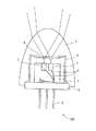
(実施形態1)
図1は実施形態1の半導体レーザ装置100を示す斜視図であり、図2Aはその断面図である。この半導体レーザ装置100は、2つの半導体レーザチップ1、2が通常の半導体レーザ用パッケージに実装され、パッケージ全体が樹脂3によってモールドされている。半導体レーザチップ1、2はパッケージの金属製ステム5と一体成形されたヒートシンク4に固着されており、良好な放熱特性を有している。本実施形態では、このパッケージの熱抵抗を90deg/Wとした。半導体レーザチップ1、2のヒートシンク4に固着されていない面は、共通のリードピン6とワイヤ7により電気的に接続されている。従って、半導体レーザチップ1、2は並列接続され、同時に電流が供給されて同期して発光する。
【0059】
一般に、半導体レーザチップ1、2は発光スポットサイズが数μmと非常に小さいため、レンズ等で集光された場合に光密度が高くなり、網膜を損傷するおそれがある。そこで、半導体レーザチップの出射光を空間に放射するときには、国際規格IEC60825−1が定められており、これを満たす範囲であれば安全性が確保される。
【0060】
本実施形態では、半導体レーザチップの発光スポットサイズを大きくするために、光拡散性の樹脂3でモールドするという手法を用いてその実現を試みた。その結果、発光スポットは約10mmまで広がり、目に対する安全性が確保された。ここでは、光拡散性樹脂3として、エポキシ系透明樹脂にそれとは屈折率が異なるシリカ系樹脂を混合したものを用いた。
【0061】
さらに、半導体レーザチップ1、2に樹脂モールドを施す前に、キャップガラス8を有するキャップ9によって封止した。これにより、半導体レーザチップ1、2が窒素ガスで封入され、信頼性が向上した。比較のために、キャップ9を用いずに半導体レーザチップ1、2をそのまま樹脂モールドすることも検討したが、この場合には半導体レーザチップが短時間で劣化した。これは、樹脂3をモールドする際の歪みが半導体レーザチップ1、2にかかることが原因であると考えられ、半導体レーザチップ1、2と樹脂3が接触しないようにするのが好ましいことがわかる。
【0062】
本実施形態では光拡散性の樹脂3のみでスポットサイズを拡大したが、同様の効果があれば他の方法を用いることも可能である。例えば、図2Bに示すように、半導体レーザのキャップガラス8の代わりに光拡散板15を用いることもできる。光拡散板15としては、ガラス表面に凹凸をつけてすりガラス状にしたもの等が用いられる。この場合、上に形成する樹脂3の拡散効果は少なくてよいからシリカ系樹脂等の拡散材の混合は少しでよいことになる。また、樹脂モールドで拡散する場合でも均一に拡散材を混合するのではなく、部分的に拡散材を多く混合し、他の領域では薄くする等でも同様の効果が得られる。
【0063】
ところで、例えば40Mbpsで8m程度の光伝送を±15゜の放射角で実現するためには、約350mWの光出力が必要となるが、単一の素子でこれだけの光出力を放射した場合、半導体レーザチップの信頼性が大きく低下する。本実施形態では、半導体レーザチップを2個用いた半導体レーザ装置100を作製しているため、2個の半導体レーザチップ1、2でこの光出力を分担することができ、1チップ当たりの光出力は175mWで良いことになる。半導体レーザチップの信頼性を確認したところ、平均故障時間は光出力の2乗に反比例し、信頼性は4倍向上することが確認された。さらに信頼性を向上させるためには、チップ数を増加させればよいことは言うまでもない。
【0064】
本実施形態では、全ての半導体レーザチップ1、2が980nm帯で発振するようにした。さらに、760nm〜1.5μm帯の半導体レーザチップを用いて実験を行ったところ、他の波長帯と比較して非常に高い信頼性を確保することが可能であった。さらに、放射特性の経時変化について調べたところ、この波長帯からなる素子のみが安定した特性を有していることがわかった。この原因については明らかではないが、他の波長帯では樹脂に対する光損傷が起こっているためと推測される。
【0065】
さらに、上記範囲内で半導体レーザチップの波長を変化させて光伝送特性を調べたところ、約900nm近傍、約1.1μm近傍および約1.4μm近傍のいずれかで実験を行ったときが最も雑音が少なく、良好な光伝送を実現することができた。この理由については明らかではないが、特に屋外での実験において顕著な効果が得られたことから、背景光強度、おそらく太陽光の影響がこの波長範囲で極小になることに起因すると考えられる。
【0066】
本実施形態の半導体レーザ装置100を用いて40Mbps、8mの光伝送を試みたところ、LEDを用いた場合と比較して、消費電力は約1/3であり、大幅な低消費電力化を実現することができた。また、高速伝送実験を試みたところ、伝送距離は短くなるものの、100Mbpsはもちろん、1Gbpsにおいても安定した伝送特性を示した。
【0067】
本実施形態においては熱抵抗が90deg/Wのパッケージを用いたが、数種類のパッケージを用いてこの値を変化させ、信頼性の確認を行った結果、熱抵抗が150deg/Wを超える場合、初期に素子劣化が生じることが確認された。熱抵抗が150deg/W以下の場合には安定した信頼性を示し、特に、100deg/W以下においては極めて良好な信頼性が得られた。
【0068】
ただし、使用条件によってはこれほどの高信頼性を要求されない場合もあり、その場合には熱抵抗の大きいパッケージでも充分である。例えば、発光ダイオード用のリードフレームに半導体レーザチップを搭載して同様の樹脂モールドを施した素子を作製したところ、携帯情報端末で瞬間的に使用するような用途においては充分な信頼性を示した。
【0069】
さらに、複数の半導体レーザチップを並列接続して駆動した場合、全体の素子抵抗が減少して駆動電圧が低下することが確認された。本実施形態では、3V以下の駆動電圧で駆動回路を構成することができ、低消費電力化を実現することができた。
【0070】
さらに、本実施形態による半導体レーザ装置100は、スポットサイズと放射角の制御に有効である。このことについて以下に説明する。
【0071】
本発明のように、半導体レーザチップ1、2の出力光を光拡散機能を有する樹脂3によって拡散させる場合には、樹脂3内部を光が通過する距離が長い程、樹脂3から出射されたときの光のスポットサイズが大きくなる。目に対する安全性の観点から考えると、このスポットサイズはできるだけ大きい方が望ましい。ところが、スポットサイズを大きくするために樹脂3内部を光が通過する距離を長くすると、当然のことながら、最終的な放射角も大きくなる。しかし、必要以上に放射角が大きくなると、有効に利用される光の割合が小さくなり、消費電力が大きくなるという問題が発生する。
【0072】
これに対して、本実施形態のように複数の半導体レーザチップを搭載した場合には、単一の半導体レーザチップの場合に比べて樹脂3内部通過距離が同じでも、図2Aに示すように、発光点の位置が離れている分だけ発光スポットサイズが大きくなる。従って、所望のスポットサイズを得るための樹脂モールドの大きさが小さくてもよく、その分だけ放射角を狭くすることができる。すなわち、本実施形態において、複数の半導体レーザチップ間の距離と、樹脂モールドの大きさを調整することにより、発光スポットサイズと放射角とを制御することが可能となる。
【0073】
例えば、単一の半導体レーザチップを樹脂モールドした場合、放射角を±15゜に設定すると発光スポットサイズは約7mmとなり、放射角を±10゜に設定すると発光スポットサイズは約5mmとなった。同じ放射角でより高い光出力が要求される場合には、スポットサイズをさらに大きくする必要があるが、単一の半導体レーザチップでは、放射角を同じに保ったまま発光スポットサイズのみを大きくすることは不可能であった。すなわち、発光スポットサイズを大きくするためには樹脂内部での光の拡散を強くする必要があり、樹脂中の拡散材、例えばシリカ系樹脂の量を多くする必要がある。しかし、これは放射角を大きくすることにつながるため、放射角とスポットサイズとを独立に制御することができない。
【0074】
これに対して、複数の半導体レーザチップを用いた場合について、例えば、放射角±15゜、発光スポットサイズ約7mmの条件で樹脂3を形成する場合を考える。2つの半導体レーザチップの発光点を3mm離して配置すると、各発光点からの放射光は単一の半導体レーザチップの場合と同様に拡散され、発光スポットサイズが各々7mm、放射角が±15゜となる。このとき、スポットサイズ7mmのものが2つ平行に配置されているため、実際に半導体レーザ装置100の外部から観察したときのスポットサイズは約10mmとみなすことができる。このように、半導体レーザチップ間の間隔を大きくすると、基本的には外部から見たスポットサイズが大きくなる。但し、半導体レーザチップ1、2間の間隔をあまり大きくしすぎると、双峰の光強度分布になるため、注意する必要がある。ここでは、横方向に半導体レーザチップを2個配置した場合について説明したが、さらに半導体レーザチップの個数を増やすことにより、発光スポットの光強度分布を適切に調節することができ、上述のような双峰の発光強度分布を補正することも可能である。さらに、パッケージを工夫することにより、縦方向に半導体レーザチップを複数個配置することも可能である。
【0075】
また、もっと狭い放射角が望ましい場合には、光拡散性の樹脂3の量を減らしておいて、同様の調整を行えばよい。このように、複数の半導体レーザチップの数、その配置、拡散性の樹脂量や樹脂モールドの大きさ等を調整することにより、放射角と発光スポットを独立して制御することができる。
【0076】
狭放射角で使用可能な状況においては、同じ光伝送速度および伝送距離を考えた場合、その分だけ低い光強度によって対応することができるので、半導体レーザチップの信頼性を大幅に向上することができる。例えば、±10゜で40Mbps、8mの光伝送を行う場合には160mWの光出力で良いため、2個の半導体レーザチップ1、2で光出力を分担すると、1個当たり80mWの光出力で良く、飛躍的な信頼性の向上が確認された。この場合にも、半導体レーザチップの個数をさらに増やしたり、または半導体レーザチップ間の距離をさらに大きくする等の方法によって、さらに狭放射角を実現することができることは言うまでもない。さらに、場合によっては、半導体レーザチップを光の放射方向を図に示される真上方向から傾けて搭載することも有効である。
【0077】
本実施形態では、1つのモールド樹脂3内に同一の波長で発振する半導体レーザチップを複数個封入した例について具体的に説明したが、複数の半導体レーザチップから発振される波長は異なってもよい。例えば910nmと950nmでそれぞれ発振する2つの半導体レーザチップを1つのモールド樹脂3内に封入した場合を考える。この半導体レーザチップを送信側のシステムに搭載し、受信側システムには2つの波長を独立して受信できる2つの受光素子を搭載しておく。受信側での波長の分離は帯域フィルタなどを利用すれば可能である。この場合の2波長の有効な使い方としては、広帯域の信号、例えば映像信号を2つに分割し、それぞれを2つのレーザで同時に送信するという方法が可能である。この方法によれば、1個の半導体レーザの送信可能な帯域では不足するような情報を2個のレーザを用いることで送信することが可能となる。2つの信号は波長分離の方法で独立して送信することができる。
【0078】
(実施形態2)
図3は本実施形態2の半導体レーザ装置300を示す断面図である。本実施形態においては、半導体レーザチップとして、複数の発光部を有するマルチストライプ型半導体レーザ(いわゆる半導体レーザアレイ)11を用いている。この図では、発光部のストライプを図示せず、発光パターンのみを図示している。
【0079】
この半導体レーザ装置300においては、発光部(ストライプ)が複数あることから半導体レーザチップの抵抗値が減少し、駆動電圧を低減することが可能となる。また、発光部間の距離を調節することにより、実施形態1と同様に、放射角を抑制しながら発光スポットサイズを拡大することが可能となる。さらに、半導体レーザチップの光出射端面における光密度を減少させることができるので、単一の半導体レーザでありながら信頼性が確保されるという点で有利である。本実施形態において、ドライエッチングによりストライプを傾斜させてミラーを形成するということも有効である。
【0080】
さらに、幅広ストライプレーザを用いて半導体レーザチップの光出射端面における光密度を減少させることもでき、この場合にも単一の半導体レーザでありながら信頼性が確保されるという点で有利である。
【0081】
本発明者らがストライプ幅を変化させて実験を試みたところ、760nm〜1.5μmの波長帯の半導体レーザチップにおいて、ストライプ幅が7μm以上であれば、スポットサイズと放射角の制御が容易であることが確認された。また、ストライプ幅間隔を調整することによりスポットサイズと放射角の制御が容易になる。さらに、この波長帯においては、放射特性の経時変化もなく、他の波長帯と比較して格段に良好な特性が得られることが確認された。
【0082】
上記実施形態1および実施形態2では、半導体レーザ装置を単体の送信ユニットとして用いる場合について説明したが、図16に示したような従来の送受信ユニット1600に適用した場合についても、同様の効果が得られた。この送受信ユニットを用いて構成した空間光伝送システムは、非常に安定した動作が可能であり、その信頼性も良好であった。さらに、センサー用光源等としても、放射角およびスポット径を調整して有効に利用可能であり、安定した動作が得られた。
【0083】
また、上記実施形態1および実施形態2では、複数の半導体レーザを並列に接続して駆動させる場合のみを示したが、複数の半導体レーザを直列に接続して駆動しても同様の効果が得られることは言うまでもない。但し、並列に接続した場合には、抵抗値の低下は生じない。
【0084】
(実施形態3)
図4は実施形態3の半導体レーザ装置400を示す斜視図である。本実施形態においては、実施形態1と同様に、2個の半導体レーザチップ12、13を半導体レーザ用パッケージに実装しているが、下記の点で実施形態1と異なっている。
1.半導体レーザチップ12、13は異なる発振波長を有している。本実施形態では、半導体レーザチップ12は980nm、半導体レーザチップ13は920nmとした。
2.半導体レーザチップ12、13は異なるリードピン6、66に各々ワイヤ7で接続されている。従って、このパッケージは、実施形態1よりもリードピンが1本増えている。
【0085】
次に、この半導体レーザ装置400を備えた送受信ユニット500、およびその送受信ユニットを用いた空間光伝送方式について、図5Aを用いて説明する。この送受信ユニット500は、送信ユニット521、第1の受信ユニット522および第2の受信ユニット523を備える。また、本実施形態において、送信ユニット521として、半導体レーザ装置400が使用される。第1の受信ユニット522は、樹脂3aおよび受光素子24aを備える。第2の受信ユニット523は、樹脂3bおよび受光素子24bを備える。
【0086】
送信ユニット521には、図4に示した異なる2つの発振波長を有する半導体レーザチップ12、13が内蔵され、樹脂3でモールドされている。受信ユニット522、523は、シリコンから構成される同じ受光素子24a、24bを内蔵しているが、それをモールドしている樹脂3a、3bが異なっている。第1の受信ユニット522は波長950nm以下の光を透過しない樹脂3aを用いており、第2の受信ユニット523は波長900nm以下の光を透過しない樹脂3bを用いている。
【0087】
この送受信ユニット500を2個用いて双方向の通信を行う光伝送システム550の実施形態を図5Bを用いて説明する。説明を明瞭化するため、便宜上、2つの送受信ユニットを参照符号501、502として参照することで区別する。相手側の送受信ユニット502から送信される信号を送受信ユニット501が受信する場合を想定する。送受信ユニット501が、送信ユニット521A、第1の受信ユニット522A、第2の受信ユニット523Aを備え、送受信ユニット502が、送信ユニット521B、第1の受信ユニット522B、第2の受信ユニット523Bを備えると仮定する。
【0088】
相手側の送受信ユニット502から信号光530が到達する場合、相手側の送受信ユニット502の送信ユニット521Bも980nmと920nmの2つの発振波長を有する半導体レーザチップ12、13を内蔵しているため、半導体レーザチップ12、13のいずれを用いて送信してくるかは不明である。そこで、送られてきた信号光530を送受信ユニット501の第1の受信ユニット522Aまたは第2の受信ユニット523Aが受信したときに、以下のように、第1の受信ユニット522Aおよび第2の受信ユニット523Aの受信レベルをチェックすることにより、送受信ユニット501は相手側の送受信ユニット502の送信ユニット521Bが送信してきている光530の波長を判別する。
【0089】
状態1:送受信ユニット501が、第1の受信ユニット522Aおよび第2の受信ユニット523Aの両方で信号光530を受信した場合、相手側の送受信ユニット502の送信ユニット521Bは980nmのレーザ光を用いて送信してきていることがわかる。
【0090】
状態2:送受信ユニット501が、第1の受信ユニット522Aは信号光を受信せず、第2の受信ユニット523Aが信号光530を受信した場合、相手側の送受信ユニット502Bは920nmのレーザ光を用いて送信してきていることがわかる。
【0091】
相手側の送受信ユニット502から送信がある場合には上記2つの状態しかあり得ないから、これにより相手側の送受信ユニット502の送信ユニット521Bが用いているレーザ光530の波長を判別することが可能である。この程度の判別は瞬時に行うことができるので、これを基にして、送受信ユニット501の送信ユニット521Aから相手側の送受信ユニット502への送信に使用するレーザ光540の波長が決定される。この波長は、以下のように、相手側の送受信ユニット502の送信ユニット521Bが用いている波長とは異なる波長に設定される。
【0092】
上記状態1の場合には、送受信ユニット501は920nmの波長を用いて送信する。このとき、送受信ユニット501の送信ユニット521Aからの送信光は送受信ユニット501の第1の受信ユニット522Aに受信されず、第2の受信ユニット523Aによってのみ受信される。従って、送受信ユニット501は第1の受信ユニット522Aを用いて相手側の送受信ユニット502の送信ユニット521Bからのレーザ光530を信号として受信すれば、送受信ユニット501の送信ユニット521Aの送信信号の影響を受けることなく受信することができる。但し、相手側の送受信ユニット502は相手側の送受信ユニット521Bから送信される送信信号を送受信ユニット502の受信ユニット522B、523Bで必ず受信してしまう。よって、送受信ユニット501のみが同時に送受信を行うことができる。
【0093】
上記状態2の場合には、送受信ユニット501は980nmの波長を用いて送信する。このとき、送受信ユニット501の送信ユニット521Aからの送信光は送受信ユニット501の第1の受信ユニット522Aおよび第2の受信ユニット523Aの両方で受信されてしまう。よって、相手側の送受信ユニット502のみが同時に送受信を行うことができる。
【0094】
上記実施形態では、同一の送受信ユニット500を使用したが、汎用的な送受信ユニットを用いることで、全2重通信が可能となり、安価な送受信ユニットを大量に作成することができる。ただし、本発明は、信号を送受信する送受信ユニットが同一であることに限定されるものではなく、少なくとも一方の送受信ユニットが全2重通信を行うために、受信ユニットの受信波長が限定されるものを包含する。
【0095】
(実施形態4)
本実施形態では、常に全2重通信が可能となる空間光伝送方式について説明する。図6Aは実施形態4の空間光伝送ユニット600を示す断面図である。空間光伝送ユニット600は、送信ユニット(図示せず)および第1の受信ユニット622、第2の受信ユニット623を備える。本実施形態において、実施形態3と異なる点は以下の通りである。
1.モールド樹脂は波長選択性を有さない。
2.第1の受信ユニット622および第2の受信ユニット623の受光素子624の直上に第1の波長選択フィルタ625、第2の波長選択フィルタ626が設けられている。
3.第1の波長選択フィルタ625は950nm以上の光を透過し、第2の波長選択フィルタ626は950nm以下の光を透過する。
【0096】
この送受信ユニット600を2個用いて双方向の通信を行う場合を考える。説明を明瞭化するため、便宜上、2つの送受信ユニットを参照符号601、602として参照することで区別する(図6B)。相手側の送受信ユニット602から送信される信号を送受信ユニット601が受信する場合を想定する。送受信ユニット601が、送信ユニット621A、第1の受信ユニット622A、第2の受信ユニット623Aを備え、送受信ユニット602が、送信ユニット621B、第1の受信ユニット622B、第2の受信ユニット623Bを備えると仮定する。
【0097】
相手側の送受信ユニット602Bから信号光が到達する場合、相手側の送受信ユニット602Bの送信ユニット621Bも980nmと920nmの2つの発振波長を有する半導体レーザチップ12、13を内蔵しているので、どちらの波長を用いて送信してくるかは不明である。そこで、送受信ユニット601が送られてきた信号光を受信したときに、以下のように、第1の受信ユニット622Aおよび第2の受信ユニット623Aの受信レベルをチェックすることにより、送受信ユニット601は相手側の送受信ユニット602の送信ユニット621Bが送信してきている光の波長を判別する。
【0098】
状態1:送受信ユニット601の第1の受信ユニット622Aが信号光を受信し、第2の受信ユニット623Aは信号光を受信しない場合、相手側の送受信ユニット602の送信ユニット621Bは980nmのレーザ光を用いて送受信ユニット601に送信してきていることがわかる。
【0099】
状態2:送受信ユニット601の第1の受信ユニット622Aは信号光を受信せず、第2の受信ユニット623Aが信号光を受信した場合、相手側の送受信ユニット602の送信ユニット621Bは920nmのレーザ光を用いて送受信ユニット601に送信してきていることがわかる。
【0100】
相手側の送受信ユニット602の送信ユニット621Bからの送信がある場合には上記2つの状態しかあり得ないから、これにより相手側の送受信ユニット602の送信ユニット621Bが用いるレーザ光の波長を判別可能である。この程度の判別は瞬時に行うことができるので、これを基にして、送受信ユニット601の送信ユニット621Aから相手側の送受信ユニット602への送信に使用するレーザ光の波長を決定する。この波長は、以下のように、相手側の送受信ユニット602の送信ユニット621Bが用いている波長とは異なる波長に設定する。
【0101】
上記状態1の場合には、送受信ユニット601の送信ユニット621Aは920nmの波長を用いて送信する。このとき、送受信ユニット601の送信ユニット621Aからの送信光は送受信ユニット601の第1の受信ユニット622Aに受信されず、第2の受信ユニット623Aによってのみ受信される。従って、送受信ユニット601が第1の受信ユニット622Aを用いて相手側の送受信ユニット602の送信ユニット621Bからの信号を受信すれば、送受信ユニット601の送信信号の影響を受けることなく受信することができ、全2重通信が可能となる。
【0102】
上記状態2の場合には、送受信ユニット601の送信ユニット621Aは980nmの波長を用いて送信する。このとき、送受信ユニット601の送信ユニット621Aからの送信光は送受信ユニット601の第1の受信ユニット622Aによって受信され、第2の受信ユニット623Aには受信されない。従って、送受信ユニット601が第2の受信ユニット623Aを用いて相手側の送受信ユニット602の送信ユニット621Bからの信号を受信すれば、送受信ユニット601の送信ユニット621Aの送信信号の影響を受けることなく受信することができ、全2重通信が可能となる。
【0103】
従って、いずれの場合にも相手側の送受信ユニット602の送信ユニット621Bからの信号光の波長を瞬時に判別することにより、送受信ユニット601の送信ユニット621Aからの送信に用いる半導体レーザを決定し、それを用いて送受信ユニット601が相手側の送受信ユニット602へ送信することにより全2重通信が可能となる。
【0104】
本実施形態では、2つの波長フィルタの一方が特定の波長(950nm)以上の光を透過し、2つの波長フィルタの他方が特定の波長(950nm)以下の光を透過するが、波長フィルタの範囲はこれに限定されない。本発明は、2つの波長フィルタが透過する光の波長範囲が重ならない場合を包含する。また、波長フィルタとしてバンドパスフィルタを使用してもよいことは当業者には明らかである。
【0105】
さらに送信用の半導体レーザとして3個以上の異なる波長を有するものを用いた場合、受光素子に設ける波長フィルタとして少なくとも1つのバンドパスフィルタを用いれば、3局以上の同時通信も原理的には可能となる。
【0106】
次に、信号の送受信開始に至るまでのコネクション形成手順について、さらに詳しく説明する。ここでは、端末Aと端末Bの間の送受信を考える。両端末には、実施形態1および実施形態2で説明したようなλ1とλ2の2波長を送信可能な複数の半導体レーザまたは多波長レーザと、これらの波長を判別可能な判別手段を有する受光素子とが装備されているものとする。
【0107】
まず、端末Aが先に送信を開始した場合のコネクション形成手順について、図7を参照しながら説明する。この図7においては、時間の経過は上から下に示される。
【0108】
ステップ1において、端末Aは他の端末からのデータ信号光や送信要求信号光等が検出されていないことを確認した上で、波長λ1の光を用いて送信要求信号を端末Bに送出する。
【0109】
ステップ2において、端末Bは端末Aからの送信要求信号を確認した後、送信側に受信したことを告げる受信応答信号を波長λ2を用いて送出する。
【0110】
ステップ3において、端末Aは端末Bからの受信応答信号を確認し、これによりコネクションが確立される。
【0111】
これ以降、端末Aは波長λ1の光を用いて送信し、波長λ2の光を受信する。また、端末Bは波長λ2の光を用いて送信し、波長λ1の光を受信する。このように波長分割を行ってデータ送受信を全2重双方向に行うことができる。端末Bが先に送信を開始した場合も、同様の手順で全2重双方向通信が可能となる。
【0112】
次に、端末Aと端末Bが同時に波長λ1の送信を開始した場合のコネクション形成手順について、図8を参照しながら説明する。この図8においても、時間の経過は上から下に示される。
【0113】
ステップ1において、端末Aと端末Bが両方共、他の端末からのデータ信号光や送信要求信号光等が検出されていないことを確認した上で、同時に波長λ1の光を用いて送信要求信号を送出した場合を考える。この場合、波長λ1の光を送信に用いているため、両端末とも自動的に、波長λ1の受光素子は受光することができない状態に設定される。
【0114】
ステップ2において、両端末とも、波長λ1の光を受光することができないため、光が検出されず、受信応答待ち時間の状態が継続する。このとき、各端末の応答待ち時間はランダム設定としてあり、送信要求を行う度に応答待ち時間が変化する。従って、端末Aおよび端末Bのうちのどちらか一方が先にタイムアウトすることになる。
【0115】
ここで、端末Aが先にタイムアウトした場合を考えると、ステップ3においてタイムアウトした端末Aは波長λ1の受光が可能となり、再度端末Bから送出された波長λ1の光検出を確認する。
【0116】
この波長λ1の光検出の確認に基づいて、ステップ4において、端末Aは受信応答信号を波長λ2を用いて送出する。
【0117】
ステップ5において、端末Bは端末Aからの受信応答を確認し、これによりコネクションが確立される。
【0118】
コネクションが確立された以降は、図7と同様、波長分割を行ってデータ送受信を全2重双方向で行うことができる。コネクションが確立できない場合には応答待ち時間をランダムに変化させて初めから再度トライする。これにより、どのような状況においても最終的にはコネクションが確立される。
【0119】
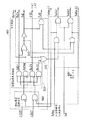
以上の手続きを自動的に行うための通信装置950のブロックダイアグラムを図9に示す。通信装置950は、制御装置900、発光モジュール420および受光モジュール410を備える。発光モジュール420として、上記の異なる半導体レーザチップを有する半導体レーザを使用してもよい。また、受光モジュールとして、上記で説明した送受信ユニットの受信ユニット部分が使用され得る。このように構成された制御装置900と、上記発光モジュール420および受光モジュール410を用いることにより、全2重の光伝送を実現することができる。以下に、この通信装置950の動作について説明する。
【0120】
受光モジュール410は単一波長受光素子411、412を備え、単一波長受光素子411はλ1の波長選択フィルタ機能を有し、単一波長受光素子412はλ2の波長選択フィルタ機能を有する。ここでは、各素子をパッケージ化して受光モジュール410を形成しているが、別々のパッケージに分離しても構わない。
【0121】
制御装置900は、光検出部と、判別部と、復調部と、選択部490とを備える。図9において、光検出部として、受信キャリア検出回路431、432が使用され、判別部として判別回路450が使用され、復調部として、復調回路480が使用される。選択部490は、送信セレクタ460および送信駆動回路441、442を含む。
【0122】
受信キャリア検出回路431は、受光素子411の信号を受けて受信した波長λ1の信号が有効であるかどうかを判断し、有効であればそれを示す信号(λ1DET)を判別回路450に出力する。受信キャリア検出回路432は、同様に、受光素子412の信号を受けて受信した波長λ2の信号が有効であるかどうかを判断し、有効であればそれを示す信号(λ2DET)を判別回路450に出力する。
【0123】
判別回路450は、受信信号の波長を判別して、受信可能であれば受信イネーブル信号(RxE)と、有効な受信信号のみを復調回路480に導くための受信セレクタ信号(λSEL)とを出力すると共に、送信制御信号(TxSel)を出力する。送信制御信号(TxSel)は、送信要求信号(TxReq)がアクティブになったときに受信信号とは異なる波長の送信信号を選択する信号である。判別回路450は、他の通信装置に発光モジュール420から信号を送信したときに送信信号が回り込んで通信装置950の受光モジュール410で受信してしまい、その結果、誤動作が生じないように、通信装置950の送信時に、他の通信装置への信号の波長を受信モジュール410で受信しないように光の検出を無効にする受信検出選択回路も備えてもよい。
【0124】
本実施形態では、受信信号セレクタ470を更に有し、受信信号セレクタ470は受信セレクタ信号に基づいて有効な受信信号を選択し、復調回路480は選択された信号を復調する。
【0125】
送信セレクタ460は判別回路450の送信要求に基づいて送信する波長を選択し、該当する送信駆動回路441、442を選択する。送信駆動回路441、442は単一波長発光素子421、422をそれぞれ駆動し、単一波長発光素子421、422はそれぞれ波長λ1、λ2に対応している。ここでは、各素子をモジュール化して発光モジュール420を形成しているが、用途によっては分離してもよい。また、各素子を同時に駆動することがない場合には、送信駆動回路441、442を1個にして駆動回路の出力側にセレクタ回路を設けることにより、回路規模を小さくしても基本的な動作は同じである。また、送信用の変調回路については駆動回路441、442に含まれるが、変調方式によっては分離して送信セレクタ460の前の送信データ入力側に設けてもよい。
【0126】
この通信装置950を有効に動作させるために制御を行う判別回路450の実現には、ソフトウェアにより行う方式とハードウェアにより行う方式がある。まず、ソフトウェアにより判別回路450を実現する方式について説明する。
【0127】
単一波長発光素子421、422がいずれも送信していない状態のときは、送信要求信号(TxReq)およびλ1、λ2の検出信号(λ1DET、λ2DET)はインアクティブである。まず、λ1、λ2の検出信号の状態をチェックして、両方がインアクティブである場合には信号の受信が無く(エンプティー状態:RxEmp)、両方ともアクティブである場合にはエラー状態(RxErr)で、通信できない状態である。判別回路450は、状態に応じて、RxEmp信号またはRxErr信号を上位の通信モジュールに出力する。また、単一波長発光素子421、422のいずれかがアクティブである場合には、該当する波長の信号を受信していることを示し、制御回路450は受信イネーブル状態(RxE)と判断する。
【0128】
上位の通信モジュールによってデータの送信要求が発生した場合には、送信要求信号(TxReq)がアクティブになるか、または送信要求指示が発生する。これを受けて、上述のようにλ1、λ2の検出信号の状態をチェックし、受信状態がエンプティー状態であって、かつ、エラー状態でないときには、送信が可能である。よって、波長λ1の送信駆動回路441または波長λ2の送信駆動回路442を選択して送信を開始する(ここでは、送信駆動回路441を選択したと仮定する)。このとき、送信する光の波長λ1の回り込みや反射等により通信装置950が送信した信号を自らの受光モジュール410(受光素子411)で受信してしまうと、単一波長光による全2重通信ができない。従って、送信開始後は、送信している波長(λ1)を自らの受光モジュール410(受光素子411)が検出する受信キャリア検出回路(431)の出力を無効にするか、または上述した受信状態の判定方法を変える必要がある。この状態では、相手の通信装置が波長λ2の光で応答してくるのを待てば良いから、判別回路450は、受信キャリア検出回路432の出力(λ2DET)を監視すると共に、受信セレクタ信号(λSEL)によって受信信号セレクタ470を波長λ2に切り替えて受信信号を復調できるようにする。波長λ2を検出する受信キャリア検出回路432の出力がアクティブになれば、全2重通信路が確立し、通信を開始することができる。
【0129】
一方、受信側の動作は、以下の通りである。通信が始まっていないので、上述のようにλ1、λ2を検出する受信キャリア検出回路431、432の出力λ1DET、λ2DETは、インアクティブでエンプティー状態であり、受信待ちの状態である。そして、相手の通信装置が送信を開始して例えば波長λ1の光を送出してくると、波長λ1を検出する受信キャリア検出回路431の出力がアクティブになる。このとき、波長λ2の光が受信キャリア検出回路432によって検出されるとエラー状態となって通信ができない。受信キャリア検出回路431の出力のみがアクティブである場合には、この通信装置950は受信可能であるので信号セレクタ470をλ1に切り替えて波長λ1の信号を復調回路480に接続する。そして、受信イネーブル信号をアクティブにするか、または受信イネーブルの指示を上位通信モジュールに伝える。上位通信モジュールはこれを受けて受信状態であることを知り、通信応答に向けた送信要求を行う。そして、この通信装置950に対する送信要求があれば、現状態では波長λ2の信号が用いられていないことが判断できるので、波長λ2に対応する送信駆動回路442を駆動し、発光素子422を用いて受信応答信号を送信する。この受信応答信号の送信中は、光の回り込み現象のために波長λ2を検出する受信キャリア検出回路432の出力がアクティブになるため、この出力を無効にするか、または上述した受信状態の判定方法を変える必要がある。このようにして全2重通信路が確立し、双方向のデータ通信を開始することができる。
【0130】
なお、同時発信した場合に衝突を回避するための通信プロトコルについては、上位の通信モジュールにより実現することができ、ランダムな応答時間を設定するタイマーについても同様に上位の通信モジュールにより実現することができる。これらの動作については、上述した通りである。
【0131】
次に、ハードウェアにより判別回路450および送信セレクタ460を実現するための回路構成の一例について、図10を参照しながら説明するが、同じような機能を有する回路であれば、実現方法はこれに限られない。
【0132】
判別回路450は、送信時に信号の回り込みによる誤判定を防止するために、受信検出選択回路560、受信波長判別回路505および汎用ゲート510、515から構成される。ここで、送信セレクタ460および判別回路450からの入出力インターフェースは、基本的に図9に示した信号と合わせてあり、基本的な動作はソフトウェアによる制御と同じである。
【0133】
両方の発光素子421、422が送信していない状態のときは、送信要求信号(TxReq)およびλ1、λ2の検出信号(λ1DET、λ2DET)はインアクティブである。よって、各波長の光に対応する送信要求信号TxReqλ1、TxReqλ2はインアクティブであり、λ1DET、λ2DET信号は、受信検出選択回路560のAND回路の入力に論理反転されて入力されていることから、受信検出選択回路560を通過して受信波長判別回路505に導かれている。受信波長判別回路505は、この信号を検査して両方がインアクティブのときには信号の受信が無いエンプティー状態(RxEmp)、両方ともアクティブのときにはエラー状態(RxErr)で通信できない状態と判断し、どちらかがアクティブである場合に該当する波長の信号を受信していることを示す状態(Rxλ1またはRxλ2)と判断する。よって、受信波長判別回路505での判定の結果、RxEmpがアクティブとなればエンプティー状態であることが分かり、RxErrがアクティブとなればエラー状態であることが分かる。また、その出力は汎用ゲート510を通して受信イネーブル信号の出力となっている。この受信イネーブル信号(RxE)は、受信エラー状態(RxErr)およびエンプティー状態(RxEmp)ではインアクティブになり、どちらか一方の波長光を受信したときのみアクティブになる。
【0134】
汎用ゲート515は、受信エンプティー状態(RxEmp)で送信を開始するときに波長λ1を選択するための回路である。ここで、上位の通信モジュールによってデータの送信要求が発生した場合には、通信路が空いていること(RxEmpがアクティブ状態)を確認して送信要求信号(TxReq)をアクティブにする。この状態では、汎用ゲート515の出力はアクティブ(H)であるから、送信要求信号(TxReq)がアクティブ(H)になったときに波長λ1の光送信要求信号TxReqλ1がアクティブ(H)になり、送信データTxDがANDゲートを通過してTxDλ1に出力されて、送信駆動回路441を駆動することになる。なお、送信駆動回路の制御には送信要求信号TxReqλ1を用いても良い。このとき、送信要求信号TxReqλ1は、λ1DET信号のゲート信号となっているため、波長λ1の光の送信を開始した状態で、光の回り込みや反射等による誤検出を防止するためにλ1DET信号をインアクティブにすれば、それ以降は波長λ2の信号受信を待つ待ち状態にロックされる。この状態では、波長λ1の光は検出できなくなるため、送信セレクタ460によって波長λ2の光を送信してしまうことはない。
【0135】
この状態で相手の通信装置が波長λ1の信号を受けて波長λ2の信号で応答してきたら、受信キャリア検出回路432の出力λ2DETがアクティブ、受信波長判別回路505のRxλ2がアクティブ(H)となり、それに伴って受信イネーブル信号RxEがアクティブとなる。また、受信セレクタ信号λSELは元々Lで受信信号セレクタ470が波長λ2を選択しているので、復調回路480で復調されて受信データRxDが得られる。上位の通信モジュールは、受信イネーブル信号RxEがアクティブになることで、全2重通信路が確立したことを判断し、通信を開始することができる。このとき、Rxλ2の出力がアクティブ(H)になって汎用ゲート510の出力がLに落ちるが、汎用ゲート515の出力は変化しないために波長λ1による光の送信は変化しない。さらに、受信イネーブル信号RxEと送信要求信号TxReqをANDゲートを通すことによって、全2重通信が確立したことを示す信号FulDを出力することもできる。
【0136】
次に、受信側の動作を説明する。受信側の通信装置が受信待機状態(通信が始まっていない初期状態)で待っているとき、相手の通信装置から波長λ1の信号光を受信したとする。受信待機状態では、送信要求信号(TxReq)がインアクティブ(L)であるから、受信検出選択回路560のゲートは両方とも開いており、どちらの波長の受信光も検出することができる。この状態で波長λ1、λ2の両方の信号を受信した場合には、受信波長判別回路505でエラーと判断され、受信イネーブル信号RxEがアクティブにならない。また、どちらか一方の信号を受信したときには受信イネーブル信号RxEがアクティブとなって受信可能であることを示す。ここでは、波長λ1の光を受信していることから、受信波長判別回路505の出力Rxλ1の出力はHとなる。その信号がλSELとなることから受信信号セレクタ470は波長λ1の信号をセレクトし、復調回路480で復調して受信データRxDが得られる。上位通信モジュールが受信イネーブル信号RxEを調べて受信状態であることを確認したら、それに応答して送信要求TxReqを行う。このとき、受信波長判別回路505の出力Rxλ1はH、汎用ゲート515の出力はLであることから、波長λ2の光送信要求信号TxReqλ2がアクティブになり、波長λ2に対応する駆動回路442が駆動されて、発光素子422から波長λ2の受信応答信号が送信される。同時に、TxReqλ2は、受信検出選択回路560のλ2DET信号のゲート信号となっているためにλ2DETがインアクティブとなり、回路がロックされる。これにより、送信が波長λ2、受信が波長λ1に固定されて全2重通信が可能となる。
【0137】
以上に説明したように、ソフトウェアであってもハードウェアであっても実現方法を問わず、各波長光の受信状態を検出して相手の送信波長光を検出したときに受信可能状態かどうかを判断すると共に、検出した波長の光のみを復調させて受信データを得、応答送信要求時に検出波長とは異なる波長を自動的に選択して送信するように制御する制御装置と、異なる複数の波長を独立して発振可能な半導体レーザ装置と、各波長を選択的に受信可能な受光素子とを用いることにより、自動的に全2重通信路を実現することが可能である。
【0138】
(実施形態5)
本実施形態でも、全2重通信が可能となる空間光伝送方式について説明する。図11Aは実施形態5の空間光伝送ユニット1100を示す断面図である。本実施形態において、実施形態4と異なる点は以下の通りである。
1.送信ユニット(図示せず)は900nmと1.2μmの発信波長を有する2個の半導体レーザチップを用いている。
2.第1の受信ユニット1122はシリコン系受光素子1127を有し、波長1μm以下の光に受光感度を有する。また、第2の受信ユニット1123はインジウムガリウム砒素(InGaAs)系の受光素子1128を有し、波長1μm以上の光に受光感度を有する。
3.各受信ユニット1122、1123にフィルタは配置されていない。
【0139】
この送受信ユニットを2個用いて双方向の通信を行う場合を考える。説明を明瞭化するため、便宜上、2つの送受信ユニットを参照符号1101、1102として参照することで区別する(図11B)。相手側の送受信ユニット1102から送信される信号を送受信ユニット1101が受信する場合を想定する。送受信ユニット1101が、送信ユニット1121A、第1の受信ユニット1122A、第2の受信ユニット1123Aを備え、送受信ユニット1102が、送信ユニット1121B、第1の受信ユニット1122B、第2の受信ユニット1123Bを備えると仮定する。
【0140】
相手の送受信ユニット1102も900nmと1.2μmの2つの発振波長を有する半導体レーザチップを内蔵しているので、どちらの波長を用いて送信してくるかは不明である。そこで、送られてきた信号光を受信したときに、以下のように、送受信ユニット1101の第1の受信ユニット1122Aおよび第2の受信ユニット1123Aの受信レベルをチェックすることにより、相手の送受信ユニット1102が送信してきている光の波長を判別する。
【0141】
状態1:第1の受信ユニット1122Aが信号光を受信し、第2の受信ユニット1123Aは信号光を受信しない場合、相手の送受信ユニット1102の送信ユニット1121Bは900nmのレーザ光を用いて送信してきていることがわかる。
【0142】
状態2:第1の受信ユニット1122Aは信号光を受信せず、第2の受信ユニット1123Aが信号光を受信した場合、相手の送受信ユニット1102の送信ユニット1121Bは1.2μmのレーザ光を用いて送信してきていることがわかる。
【0143】
相手の送受信ユニット1102からの送信がある場合には上記2つの状態しかあり得ないから、これにより相手の送受信ユニット1102の送信ユニット1121Bが用いているレーザ光の波長を判別可能である。この程度の判別は瞬時に行うことができるので、これを基にして、送受信ユニット1101からの送信に使用する送信ユニット1121Aのレーザ光の波長を決定する。この波長は、以下のように、相手の送受信ユニット1102の送信ユニット1121Bが用いている波長とは異なる波長に設定する。
【0144】
上記状態1の場合には、送受信ユニット1101の送信ユニット1121Aは1.2μmの波長を用いて送信する。このとき、送受信ユニット1101からの送信光は第1の受信ユニット1122Aに受信されず、第2の受信ユニット1123Aによって受信される。従って、第1の受信ユニット1122Aを用いて相手の送受信ユニット1102からの信号を受信すれば、送受信ユニット1101の送信信号の影響を受けることなく受信することができ、全2重通信が可能となる。
【0145】
上記状態2の場合には、送受信ユニット1101の送信信ユニット1121Aは900nmの波長を用いて送信する。このとき、送受信ユニット1101からの送信光は第1の受信ユニット1122Aによって受信され、第2の受信ユニット1123Aには受信されない。従って、第2の受信ユニット1123Aを用いて相手の送受信ユニット1102の送信ユニット1121Bからの信号を受信すれば、送受信ユニット1101の送信信号の影響を受けることなく受信することができ、全2重通信が可能となる。
【0146】
従って、いずれの場合にも相手の送受信ユニット1102の送信ユニット1121Bからの信号光の波長を瞬時に判別することにより、送受信ユニット1101からの送信に用いる半導体レーザチップの波長を決定し、それを用いて送信することにより全2重通信が可能となる。本実施形態では、受光素子の特性に波長依存性があるものを用いており、その特性に合致した半導体レーザチップを用いることにより、フィルタを用いることなく全2重通信が可能となる。
【0147】
(実施形態6)
図12に、本発明の半導体レーザ装置を赤外線送受信機601の赤外線送信機として、かつ、本発明の制御装置を通信制御装置602として用いた双方向赤外線通信装置1200a、1200bについて、誤り率を測定するための実験装置1200を示す。
【0148】
赤外線送受信機601の赤外線受信機は各波長を選択受信可能である。通信制御装置602は、マイクロコンピュータを用いて実験用の制御統制機能を実現可能としたものであり、赤外線通信装置1200a、1200bは赤外線送受信機601と通信制御装置602とを備える。
【0149】
この赤外線通信装置1200a、1200bには、送信要求のためのスイッチ603と送信停止要求のためのスイッチ604がそれぞれ設けられ、赤外線通信装置1200a、1200bを向かい合わせて送信要求スイッチ603を押すと、実施形態4で説明した通信手順を実行して全2重通信路を形成するように構成されている。LED611は通信路が全2重通信モードになったことを示し、LED612は波長λ1光の信号検出を示し、LED613は波長λ2光の信号検出を示す。
【0150】
誤り率測定装置605a、605bは赤外線双方向通信の伝送状態をチェックする。ここでは、誤り率測定装置605aからの送信データが赤外線通信装置1200aに入力され、赤外線通信装置1200aの赤外線送信機から送信され、赤外線通信装置1200bの赤外線受信機で受信された信号が受信データとして誤り率測定装置605aに入力される。誤り率測定装置605aは、送信データと受信データとの誤り率を測定する。反対に、誤り率測定装置605bからの送信データが赤外線通信装置1200bに入力され、赤外線通信装置1200bの赤外線送信機から送信され、赤外線通信装置1200aの赤外線受信機で受信された信号が受信データとして誤り率測定装置605bに入力される。誤り率測定装置605bは、送信データと受信データとの誤り率を測定する。上記のような構成により、双方向の通信状態が2台の誤り率測定装置によってチェックされ、上りと下りの伝送誤りを同時にチェックできるように実験を行った。
【0151】
この実験装置1200を用いて伝送速度100Mbps、通信距離2mで実験を行ったところ、通信装置1200aまたは通信装置1200bの送信要求スイッチ603を押すことにより双方向の送信が始まり、双方向通信状態になったことを示すLED611が点灯した。そして、誤り率計のエラーは0となり、良好な通信状態であることが分かった。
【0152】
また、送信停止スイッチ604を押すことにより両方の送信が終了し、全2重通信が可能であることが確認できた。本実施形態では100Mbpsで実験を行ったが、クロックスピードを上げることによってさらに高速の伝送が可能であることは言うまでもない。
【0153】
(実施形態7)
本実施形態では、半導体レーザチップを樹脂モールドする際に、屈折率の異なる材料の混入量や樹脂の大きさ、形状等を調整して光スポット径が1mmになるように設定し、ファイバとしてコア径1mmのPOFを用いてこれらを直接接合することを試みた。その結果、特別な工具を用いること無しに、目視で簡単に高効率の光結合を行うことが可能であった。また、半導体レーザ装置のスポットサイズと放射角を自由に調整することができるため、用途に応じた仕様で設計することが可能であった。
【0154】
なお、本実施形態では、樹脂モールド中の屈折率の異なる材料の混入量や樹脂の大きさ、形状等を調整して光スポット径が1mmになるように設定したが、別のスポットサイズが要求される場合には、複数の半導体レーザチップの間隔や、マルチストライプレーザの発光部間隔、幅広レーザの発光部幅等を調整して所望のスポットサイズを得ることも可能である。
【0155】
(実施形態8)
図13は実施形態8のファイバ系光伝送ユニット1300を示す断面図である。この光伝送ユニット1300は、ファイバとしてPOF72を用いており、その先端に光ミニプラグ71が装備されている。半導体レーザ装置70は、780nmの発信波長を有する半導体レーザチップ70aと980nmの発信波長を有する半導体レーザチップ70bとが1つのパッケージ内に実装され、全体が樹脂モールドされて発光スポットサイズ約1mmとされている。半導体レーザ装置70は光ミニジャック(OMJ)73に取り付けられ、OMJ73の内部には波長780nmの光を選択的に受信可能な受光素子74と波長980nmの光を選択的に受信可能な受光素子75が内蔵されている。本実施形態において、接続コネクタの具体例として光ミニジャック73を説明する。受光素子74、75は、半導体レーザ装置70とPOF72との間の光路内に取り付けられ、それによって半導体レーザ装置70からの出射光の一部が遮断されるが、残りがPOF72に導かれる。また、POF72からの光も、受光素子74、75に受光されるものとそれを通過して半導体レーザ装置70に戻るものに分かれる。しかし、半導体レーザチップ70a、70bは樹脂モールドされているため、戻り光のうち半導体レーザチップ70a、70bにまで戻るものは殆ど無く、戻り光雑音は確認されなかった。
【0156】
本実施形態のファイバ系光伝送ユニットを用いて映像情報の伝送を試みたところ、実施形態4で説明した手順で行うことにより、全2重通信が可能であることが確認された。
【0157】
(実施形態9)
図14は実施形態9のファイバ系光伝送ユニット1400を示す断面図である。本実施形態において、実施形態8と異なる点は、光ミニジャック73内の受光素子74、75の配置である。本実施形態においては、波長780nmの光を選択的に受信可能な受光素子74と波長980nmの光を選択的に受信可能な受光素子75が光ミニジャック73の内壁面に取り付けられている。従って、実施形態8のように半導体レーザ装置70から直進して出力された光が受光素子74、75によって遮られることなくPOF72に導かれ、高効率の光結合が実現された。また、POF72からの光はPOF72出力後に回折し、ある程度の広がり角をもって出射されるから、受光素子74、75が内壁面に取り付けられていても、充分な受光感度が得られる。その結果、半導体レーザ装置の光出力が実施形態8と比較して80%であっても、実施形態8と同様の光伝送を実現可能であった。
【0158】
さらに、本実施形態の光伝送ユニット1400により、多チャンネルケーブルテレビの配信信号を用いて映像信号の伝送実験を行った。伝送速度を1Gbps、伝送距離(ファイバ長さ)を100mとしたところ、全2重でエラーフリーの良好な伝送が確認された。同様の効果は、AV機器間の映像信号伝送に用いた場合にも確認され、本発明はこれらの信号伝送に適していることが確認された。
【0159】
【発明の効果】
以上詳述したように、本発明による場合には、半導体レーザチップと光拡散機能を有する樹脂部とが一体成形されているので、半導体レーザチップからの出射光を空間に安全に放出することができ、低消費電力で高速伝送が可能となる。
【0160】
複数の発光部を有するマルチストライプ型半導体レーザを用いるか、幅7μm以上の発光部を有する幅広ストライプ半導体レーザを用いるか、複数の半導体レーザチップを搭載することによって、素子の信頼性が飛躍的に向上し、さらに、発光スポットサイズと光放射角の制御が容易になる。
【0161】
樹脂部に屈折率が異なる材料を混入し、樹脂部を半導体レーザチップと接触しないように設けることにより、目に対する安全性を充分確保することができる。特に、半導体レーザチップを搭載する容器の熱抵抗を150deg/W以下、好ましくは、100deg/W以下とするのが効果的である。
【0162】
半導体レーザチップの複数の発光部、または複数搭載された半導体レーザチップが全て同じ波長帯域で発振するものであれば、半導体レーザ装置の信頼性を向上させることが可能となる。また、半導体レーザチップの複数の発光部または複数搭載された半導体レーザチップのうちの少なくとも2つが、異なる波長帯域で発振するものであれば、全2重通信が可能となる。
【0163】
特に、発振波長760nm以上1.5μm以下の波長帯で非常に効果的であり、約900nm、約1.1μmまたは約1.4μm近傍の波長では最も雑音が少なく良好な状態で光伝送を行うことができる。
【0164】
さらに、波長判別手段を有する受光素子を装備することにより、全2重空間光伝送システムが実現可能となる。
【0165】
異なる複数の波長の中から、相手の送受信ユニットが送信してきている波長を自動判別し、その波長以外の波長を選択して自らの送受信ユニットから送信することにより、従来では半2重であったIrDA等の光空間伝送を全2重空間光伝送とすることができる。また、伝送に用いる光の波長を予め指定しておく必要が無いので、親機と子機の区別が不要となって対称的通信が可能となり、通信相手の送受信ユニットが変わっても波長選択の設定が不要となる。また、従来複雑であった通信プロトコルの簡略化も図ることができる。また、本発明は、IEEE1394空間伝送方式にも適用可能である。
【0166】
送受信ユニットから送信する際に、発光素子が送信している波長の光を送受信ユニットの自らの受信回路が検出しないように制御すれば、送受信ユニット自らの信号の影響を受けずに受信可能であり、良好な通信状態を確保することができる。
【0167】
さらに、従来では2本のファイバを用いることが主流であったIEEE1394全2重化光通信方式を、1本のファイバを用いて実現可能することができ、半導体レーザ装置とファイバの光結合を簡単に行うことができる。
【0168】
一方の端部に発光素子(半導体レーザ装置)を配置し、他方の端部に光ファイバを配置し、接続コネクタの内部に受光素子を配置して固定するような筒状の接続コネクタを用いることにより、半導体レーザ装置や受光素子とファイバとの接続がさらに容易になる。また、この接続コネクタの内壁面に受光素子を配置すれば、半導体レーザ装置からの光が受光素子に遮られないので、信号光の利用効率が向上し、高効率の光結合が得られる。
【0169】
本発明の制御装置によれば、異なる複数の波長の中から相手の通信装置が送信してきている波長を自動判別し、その波長以外の波長を選択して自らの通信装置から送信可能な光送信システムを実現することが可能となる。
【0170】
本発明の通信装置によれば、通信相手の端末が変わっても波長選択の設定をその都度行う必要がなく、従来複雑であった通信プロトコルの簡略化を図ることができ、さらに、データの送受信を全2重双方向で行うことができる。また、各局でランダムな待ち時間を設定するプロトコルにより、同時送信状態が発生したときでもコネクション確立の衝突を回避して、どのような状況においてもコネクションを確立することができる。
【図面の簡単な説明】
【図1】実施形態1の半導体レーザ装置を示す斜視図である。
【図2A】実施形態1の半導体レーザ装置の断面図である。
【図2B】実施形態1の変形例の半導体レーザ装置の断面図である。
【図3】実施形態2の半導体レーザ装置の断面図である。
【図4】実施形態3の半導体レーザ装置を示す斜視図である。
【図5A】実施形態3の光送受信ユニットを示す斜視図である。
【図5B】実施形態3の光送受信システムを示す斜視図である。
【図6A】実施形態4の光送受信ユニットを示す断面図である。
【図6B】実施形態4の光送受信システムを示す斜視図である。
【図7】片方の端末から送信を開始した場合のコネクション形成手順を示す図である。
【図8】両方の端末から送信を開始した場合のコネクション形成手順を示す図である。
【図9】コネクション形成を自動的に行うための半導体レーザ駆動回路および受光素子の信号処理回路のブロックダイアグラムである。
【図10】図9の判別回路および送信セレクタをハードウェアで実現するための回路の一例を示す図である。
【図11A】実施形態5の光送受信ユニットを示す断面図である。
【図11B】実施形態5の光送受信システムを示す斜視図である。
【図12】実施形態6の双方向赤外線通信実験装置を示す図である。
【図13】実施形態8のファイバ系光伝送ユニットを示す断面図である。
【図14】実施形態9のファイバ系光伝送ユニットを示す断面図である。
【図15】従来のIrDAを用いた光伝送システムを示す図である。
【図16】従来のIrDAを用いた送受信ユニットを示す断面図である。
【図17】従来のファイバ系光伝送に用いられる送受信ユニットを示す断面図である。
【符号の説明】
1、2、12、13、70a、70b 半導体レーザチップ
3、3a、3b 樹脂
4 ヒートシンク
5 ステム
6、66 リードピン
7 ワイヤ
8 キャップガラス
9 キャップ
11 半導体レーザアレイ
15 光拡散板
24a、24b、74、75、624、1127、1128 受光素子
70、100、300、400 半導体レーザ装置
71 光ミニプラグ
72、1716、1717、1718 POF
73 光ミニジャック
410 受光モジュール
411、412 単一波長受光素子
420 発光モジュール
421、422 単一波長発光素子
431、432 受信キャリア検出回路
441、442 送信駆動回路
450 判別回路
460 送信セレクタ
470 受信信号セレクタ
480 復調回路
490 選択部
500、501、502、1600 送受信ユニット
505 受信波長判別回路
510、515 汎用ゲート
521、521A、521B、1601 送信ユニット
522、522A、522B、523、523A、523B、622、623、1122、1123、1602 受信ユニット
560 受信検出選択回路
600、1100 送受信ユニット
601 赤外線送受信機
602 通信制御装置
603 送信要求スイッチ
604 送信停止スイッチ
605a、605b 誤り率測定装置
611 全2重通信モード表示LED
612 λ1光信号検出を示すLED
613 λ2光信号検出を示すLED
625、626 波長選択フィルタ
900 制御装置
950 通信装置
1200a、1200b 赤外線通信装置
1500 パーソナルコンピューター
1502 携帯情報端末[0001]
BACKGROUND OF THE INVENTION
The present invention is used in applications such as wireless communication and light sources for sensors where light is emitted into space and a person directly sees the light source, and ensures safety for eyes, a semiconductor laser device, an optical transmission device, and optical transmission The present invention relates to an electronic device, a control device, a communication device, a spatial light transmission method, and a data transmission / reception method that use a spatial light transmission system such as a system, a personal computer, a portable information terminal, and a digital camera. In addition, the present invention relates to a semiconductor laser device with an enlarged light emitting spot, an optical transmission device capable of simultaneous transmission and reception, an optical transmission system, an electronic device using a fiber-based optical transmission system for multi-channel CATV, AV, etc., fiber-based light The present invention relates to a transmission system, a control device, a communication device, a fiber-based optical transmission method, and a data transmission / reception method.
[0002]
[Prior art]
Spatial light transmission using infrared rays is now widely used due to standardization and widespread use by IrDA (Infrared Data Association). For example, FIG. 15 shows an example in which spatial light transmission is used for data transmission between the
[0003]
In recent years, the transmission speed has been increasing with the increase in data capacity, and has increased from 1 Mbps to 4 Mbps, and further to 16 Mbps. In addition, there is an increasing demand for transmission distance, and transmission up to 8 m is possible by standardization of the IrDA Control standard. However, the transmission rate in this case is limited to 75 kbps. In addition, there is a movement to wirelessly transmit video information, and there is an increasing demand for higher speed and longer distance.
[0004]
On the other hand, the progress of fiber-based optical transmission technology using an optical fiber as a transmission line is also remarkable. In particular, plastic optical fiber (POF) is rapidly spreading because it is low-cost and has a large fiber diameter, so that coupling with a light-emitting element is easier than single-mode fiber. In this fiber-based optical transmission technology, transmission of 100 Mbps or more is currently realized using a semiconductor laser.
[0005]
[Problems to be solved by the invention]
Currently, in spatial light transmission, a light emitting diode (LED) is used as the light source. However, when considering further high-speed and long-distance transmission using currently available LEDs,
(1) Inability to perform high-speed modulation due to limitations of LED high-speed response characteristics; and
(2) Large amount of power consumption when performing long distance transmission
There are two problems.
[0006]
Among these, regarding the problem (1), the limit modulation frequency of a normal LED is about 50 MHz, and it is difficult to increase the speed further. Furthermore, in the case of a special LED that supports high-speed modulation, there is a problem that power consumption becomes very high. As for the problem (2), for example, when transmission at a distance of 5 m is considered at 40 Mbps, power consumption of 1 W is required only by the LED.
[0007]
On the other hand, when a semiconductor laser is used as the light source, it has an excellent feature that it can be modulated at high speed and has low power consumption for obtaining the same light output as compared with the LED. However, if a semiconductor laser is used as it is, it does not meet the safety standards for the eyes and cannot be directly emitted into space. Further, when the semiconductor laser is operated at a high output, there is a problem that reliability is lowered.
[0008]
Furthermore, the spatial light transmission system has a big problem that full duplex communication is not possible. This problem will be described below.
[0009]
Electronic devices such as the
[0010]
In this transmission /
[0011]
Next, problems of the fiber-based optical transmission system will be described.
[0012]
FIG. 17 shows an example of a transmission / reception unit at one end of a fiber-based optical transmission system using POF. In this transmission /
[0013]
Here, since the
[0014]
The present invention has been made to solve the above-described problems of the prior art, and is capable of high-speed modulation, low power consumption, high safety and reliability for eyes, suitable for spatial light transmission, and full duplex. It is an object of the present invention to provide a semiconductor laser device, an optical transmission device, an electronic device, a spatial light transmission system, a control device and a communication device thereof, a spatial light transmission method, and a data transmission / reception method capable of realizing spatial light transmission. The present invention also provides a semiconductor laser device, an optical device capable of high-speed modulation, low power consumption, easy alignment with a fiber, suitable for fiber-based optical transmission, and capable of realizing full-duplex fiber-based optical transmission. It is an object of the present invention to provide a transmission device, an electronic device, a fiber-based optical transmission system, a control device and a communication device thereof, a fiber-based optical transmission method, and a data transmission / reception method.
[0015]
[Means for Solving the Problems]
The semiconductor laser device of the present invention includes a semiconductor laser chip and a resin portion that has a light diffusion function and molds the semiconductor laser chip.
[0016]
The semiconductor laser chip may have a plurality of light emitting portions.
[0017]
The semiconductor laser chip may have a light emitting part having a width of 7 μm or more.
[0018]
There may be a plurality of the semiconductor laser chips.
[0019]
The resin part may be mixed with materials having different refractive indexes.
[0020]
The plurality of light emitting portions of the semiconductor laser chip may all oscillate in the same wavelength band.
[0021]
The plurality of semiconductor laser chips may all oscillate in the same wavelength band.
[0022]
At least two of the plurality of light emitting portions of the semiconductor laser chip may oscillate in different wavelength bands.
[0023]
At least two of the plurality of semiconductor laser chips may oscillate in different wavelength bands.
[0024]
The plurality of semiconductor laser chips may be connected in parallel.
[0025]
The optical transmission device of the present invention uses the semiconductor laser device described above as a light source.
[0026]
An optical transmission device of the present invention is an optical transmission device including a light emitting element capable of independently oscillating a plurality of different wavelengths and a light receiving element capable of selectively receiving a plurality of wavelengths, The semiconductor laser device described above is used.
[0027]
An optical transmission device according to the present invention is an optical transmission device including a light emitting element capable of independently oscillating a plurality of different wavelengths and a light receiving element capable of selectively receiving a plurality of wavelengths. Oscillation and reception of the light receiving element operate simultaneously.
[0028]
The wavelength received by the light receiving element may be determined, and the light emitting element may oscillate a wavelength other than the received wavelength.
[0029]
The number of the light receiving elements is at least two, one of the light receiving elements is molded by the first resin and the other light receiving element is molded by the second resin, respectively. It does not have to overlap with the range of wavelengths that pass through the second resin.
[0030]
There are at least two light receiving elements, a first wavelength filter is provided on one of the light receiving elements, a second wavelength filter is provided on the other light receiving element, and a wavelength that passes through the first wavelength filter. May not overlap with the range of wavelengths transmitted through the second wavelength filter.
[0031]
The wavelength range that transmits the first wavelength filter may be a specific wavelength or more, and the wavelength range that transmits the second wavelength filter may be the specific wavelength or less.
[0032]
The plurality of wavelengths oscillated by the light emitting element may correspond to the plurality of wavelengths that can be received by the light receiving element.
[0033]
There are at least two light receiving elements, and the wavelength range of the light receiving sensitivity of one light receiving element may not overlap with the wavelength range of the light receiving sensitivity of the other light receiving element.
[0034]
The wavelength range of the light receiving sensitivity of the one light receiving element may be a specific wavelength or more, and the wavelength range of the light receiving sensitivity of the other light receiving element may be the specific wavelength or less.
[0035]
An optical transmission system of the present invention includes a plurality of the optical transmission devices described above.
[0036]
An electronic apparatus according to the present invention includes the semiconductor laser device described above.
[0037]
The control device of the present invention, a light detection unit that receives the output of the light receiving element and detects the reception state of the wavelength light, a determination unit that determines whether it is in a receivable state based on the output of the light detection unit, A demodulator that demodulates the signal of the wavelength determined by the determination unit to obtain received data, a selection unit that automatically selects a wavelength different from the wavelength received by the light receiving element, and outputs the wavelength to the light emitting element unit; .
[0038]
A communication device of the present invention includes a light emitting element capable of independently oscillating a plurality of different wavelengths, a light receiving element capable of selectively receiving each wavelength, and the control device described above, a semiconductor laser chip, A semiconductor laser device having a light diffusion function and including a resin portion for molding the semiconductor laser chip is used as the light emitting element.
[0039]
The determination unit may include a reception detection selection circuit that controls so that the light receiving element does not detect light having a wavelength transmitted by the light emitting element.
[0040]
The connection connector of the present invention has a cylindrical shape having both ends, and includes a light receiving element for selecting a plurality of wavelengths inside the cylindrical shape.
[0041]
The optical transmission method of the present invention is an optical transmission method for transmitting and receiving light in an optical transmission device including a light emitting element capable of independently oscillating a plurality of different wavelengths and a light receiving element capable of selectively receiving each wavelength. A step of automatically determining the wavelength received by the light receiving element from the plurality of different receivable wavelengths, and the light emitting element selecting and transmitting a wavelength other than the wavelength received by the light receiving element. And a step of.
[0042]
In the data transmission / reception method of the present invention, the first terminal oscillates the first wavelength as a transmission request signal with respect to the second terminal, and the second transmission step receives the first wavelength. A first confirmation step in which the terminal confirms the transmission request signal; a second oscillation step in which the second terminal oscillates a second wavelength as a reception response signal to the first terminal; and The first terminal that receives the second wavelength confirms the reception response signal, and the first terminal sends the second terminal to the second terminal based on the second confirmation step. At the first wavelength, the second terminal simultaneously transmits and receives data to and from the first terminal at the second wavelength.
[0043]
The operation of the present invention will be described below.
[0044]
In the present invention, since the semiconductor laser chip and the resin portion having the light diffusion function are integrally formed, the emitted light from the semiconductor laser chip is diffused by the resin portion and safely released into the space. Therefore, spatial light transmission using a semiconductor laser capable of high-speed modulation and low power consumption compared to LEDs can be realized.
[0045]
Further, by using a multi-stripe semiconductor laser having a plurality of light emitting portions (so-called semiconductor laser array), the resistance value of the element is reduced, the driving voltage is reduced, and the light density at the light emitting end face of the semiconductor laser chip is further reduced. As a result, the reliability of the device is improved. Further, even when a wide stripe semiconductor laser having a light emitting portion having a width of 7 μm or more is used, the resistance value of the element is reduced and the driving voltage is reduced. Further, the light density at the light emitting end face of the semiconductor laser chip is reduced and the element is reduced. Reliability is improved. Alternatively, by mounting a plurality of semiconductor laser chips, the resistance value of the element is reduced and the driving voltage is reduced, and further, the optical output is shared by the plurality of semiconductor laser chips and the reliability of the element is improved.
[0046]
Light passes between the light emitting part interval of the semiconductor laser chip having such a plurality of light emitting parts, the light emitting part width of the semiconductor laser chip having a light emitting part having a width of 7 μm or more, or the chip interval of the plurality of mounted semiconductor laser chips. By adjusting the size of the resin part, the material of the resin part (amount of light diffusing material) or the shape, it is possible to obtain a desired light emission spot size and emission angle.
[0047]
The resin part can be provided with a light diffusion function by mixing materials having different refractive indexes. At this time, if the resin portion is provided so as not to come into contact with the semiconductor laser chip, the distortion during the resin molding is not applied to the semiconductor laser chip, which is preferable for improving the reliability. In particular, when the thermal resistance of the container on which the semiconductor laser chip is mounted is 150 deg / W or less, more preferably 100 deg / W or less, the reliability of the element is prevented from deteriorating and stable performance can be obtained.
[0048]
If a plurality of light emitting portions of a semiconductor laser chip or a plurality of mounted semiconductor laser chips all oscillate in the same wavelength band, the reliability of the semiconductor laser device can be improved as described above. Alternatively, as long as at least two of the plurality of light emitting portions of the semiconductor laser chip or the plurality of mounted semiconductor laser chips oscillate in different wavelength bands, full duplex communication is possible as will be described later.
[0049]
In particular, in the wavelength band of 760 nm to 1.5 μm, it is possible to ensure extremely high reliability compared to other wavelength bands, and about 900 nm, about 1.1 μm, and about 1.4 μm. It is possible to realize optical transmission in a favorable state with the least noise at a wavelength of.
[0050]
By using the semiconductor laser device of the present invention as a light source, it is possible to transmit light through the space at a high speed with low power consumption compared to the LED, and the light is diffused by the resin portion to ensure safety for eyes. Furthermore, a spatial light transmission device such as a transmission unit or a transmission / reception unit with good element reliability is realized. In addition, by using the semiconductor laser device of the present invention as a light source, light can be transmitted at high speed with low power consumption using an optical fiber as a transmission line, the reliability of the element is good, and the spot diameter is appropriately enlarged. Thus, a fiber-based optical transmission device that can be easily connected to an optical fiber is realized. Therefore, by mounting the semiconductor laser device of the present invention or the optical transmission device of the present invention on an electronic device such as a personal computer, a portable information terminal, or a digital camera, it is possible to speed up data transmission with low power consumption. . Also, as the sensor light source, the spot diameter and the radiation angle can be set in appropriate ranges, and the reliability is improved.
[0051]
By using the semiconductor laser device described above as a light emitting element, a plurality of different wavelengths can be independently oscillated, and a light receiving element capable of selectively receiving each wavelength is provided, so that a plurality of transmission / reception units can be connected. An optical transmission system capable of performing full duplex communication can be realized. For example, full duplex spatial light transmission is possible by transmitting and receiving light through a space with each transmitting and receiving unit facing each other, or full duplex by transmitting and receiving light between each transmitting and receiving unit using an optical fiber as a transmission path. Fiber-based optical transmission is possible. Depending on the application, a plurality of semiconductor laser devices in which a semiconductor laser chip and a resin portion having a light diffusion function are integrally formed as a light emitting element and on which one semiconductor laser chip is mounted may be used.
[0052]
By automatically determining the wavelength transmitted by the other transmission / reception unit from a plurality of different wavelengths, selecting a wavelength other than that wavelength and transmitting from the transmission / reception unit, IrDA or the like that was half-duplex in the past It is possible to make full-space optical transmission of the optical space transmission. In this case, there is no need to preliminarily specify the wavelength of light used for transmission, and it becomes unnecessary to distinguish between the parent device and the child device, thereby enabling symmetric communication. Furthermore, when transmitting from the transmission / reception unit, if control is performed so that the light receiving element does not detect the light having the wavelength transmitted by the light emitting element, the light can be received without being influenced by the signal of the light emitting element. Therefore, it is preferable. The present invention is also attracting attention as a next-generation multimedia interface, and can also be applied to applications such as directly making an IEEE 1394 serial bus capable of transmitting digital AV signals at high speed.
[0053]
Furthermore, the IEEE 1394 full-duplex optical communication method, which conventionally used two fibers, can be realized using one fiber.
[0054]
In fiber-based optical transmission, a cylindrical connection connector is used in which a light emitting element is arranged at one end, an optical fiber is arranged at the other end, and a light receiving element is arranged and fixed inside the connection connector. In this case, the connection between the element and the fiber is easy. If the light receiving element is disposed on the inner wall surface of the connection connector, the light from the light emitting element is not blocked by the light receiving element, so that the use efficiency of the signal light is improved.
[0055]
In the control device of the present invention, the light detection unit that receives the output of the light receiving element and detects the reception state of each wavelength light, and the reception state when the light of the wavelength transmitted by the communication partner is detected. A discriminating unit for determining whether there is a signal, a demodulating unit for demodulating a signal having a wavelength determined by the discriminating unit to obtain received data, and a wavelength different from the detected wavelength when making a transmission request in response to the communication With the selection unit that automatically selects the wavelength, it is possible to realize an optical transmission system that can automatically determine the wavelength that the partner station is transmitting from among different wavelengths and select a wavelength other than that wavelength for transmission It becomes.
[0056]
Further, in the communication device of the present invention, when making a transmission request in response to the communication, because a wavelength different from the transmission wavelength of the communication partner detected by the light receiving unit is automatically selected and transmitted, Even if the terminal of the communication partner changes, it is not necessary to set the wavelength selection each time, and it is possible to simplify the communication protocol that has been complicated in the past. Also, when detecting the light of the wavelength transmitted by the communication partner, transmit a light of a wavelength different from that and confirm that the wavelengths of the transmitted light and the received light are different from each other. By having it, it becomes possible to perform transmission and reception of data in a full-duplex bi-directional manner with surely dividing wavelengths. Furthermore, by having a protocol that sets a random waiting time in each transmission / reception unit, it is possible to avoid a collision in establishing a connection even when a simultaneous transmission state occurs. This is preferable.
[0057]
DETAILED DESCRIPTION OF THE INVENTION
Embodiments of the present invention will be described below with reference to the drawings.
[0058]
(Embodiment 1)
FIG. 1 is a perspective view showing a
[0059]
In general, since the
[0060]
In the present embodiment, in order to increase the light emission spot size of the semiconductor laser chip, the realization was attempted using a technique of molding with a
[0061]
Further, the
[0062]
In this embodiment, the spot size is enlarged only by the
[0063]
By the way, for example, in order to realize optical transmission of about 8 m at 40 Mbps with a radiation angle of ± 15 °, an optical output of about 350 mW is required. The reliability of the laser chip is greatly reduced. In this embodiment, since the
[0064]
In this embodiment, all the
[0065]
Furthermore, when the optical transmission characteristics were examined by changing the wavelength of the semiconductor laser chip within the above range, the most noise was observed when the experiment was conducted at about 900 nm, about 1.1 μm, or about 1.4 μm. Therefore, good optical transmission could be realized. Although the reason for this is not clear, it is considered that the effect of the background light intensity, possibly sunlight, is minimized in this wavelength range because a remarkable effect was obtained particularly in an outdoor experiment.
[0066]
When an attempt was made to transmit light at 40 Mbps and 8 m using the
[0067]
In the present embodiment, a package having a thermal resistance of 90 deg / W was used. However, when this value was changed using several types of packages and reliability was confirmed, if the thermal resistance exceeded 150 deg / W, the initial value It was confirmed that the device deteriorated. When the thermal resistance was 150 deg / W or less, stable reliability was exhibited. Particularly, when the thermal resistance was 100 deg / W or less, extremely good reliability was obtained.
[0068]
However, depending on use conditions, such high reliability may not be required, and in that case, a package having a large thermal resistance is sufficient. For example, when a semiconductor laser chip was mounted on a lead frame for a light emitting diode and a similar resin mold was applied, an element that was used instantaneously on a portable information terminal showed sufficient reliability. .
[0069]
Further, it was confirmed that when a plurality of semiconductor laser chips are connected in parallel and driven, the overall device resistance decreases and the drive voltage decreases. In this embodiment, the drive circuit can be configured with a drive voltage of 3 V or less, and low power consumption can be realized.
[0070]
Furthermore, the
[0071]
When the output light of the
[0072]
On the other hand, when a plurality of semiconductor laser chips are mounted as in this embodiment, even if the
[0073]
For example, when a single semiconductor laser chip is resin-molded, the emission spot size is about 7 mm when the emission angle is set to ± 15 °, and the emission spot size is about 5 mm when the emission angle is set to ± 10 °. When higher light output is required at the same emission angle, it is necessary to increase the spot size, but in a single semiconductor laser chip, only the emission spot size is increased while keeping the emission angle the same. It was impossible. That is, in order to increase the light emission spot size, it is necessary to increase the diffusion of light inside the resin, and it is necessary to increase the amount of the diffusion material in the resin, for example, a silica-based resin. However, since this leads to an increase in the emission angle, the emission angle and the spot size cannot be controlled independently.
[0074]
On the other hand, in the case where a plurality of semiconductor laser chips are used, for example, a case where the
[0075]
If a narrower radiation angle is desired, the same adjustment may be performed while reducing the amount of the
[0076]
In situations where a narrow emission angle can be used, considering the same optical transmission speed and transmission distance, it is possible to cope with a lower light intensity, which can greatly improve the reliability of the semiconductor laser chip. it can. For example, when optical transmission of 40 Mbps and 8 m is performed at ± 10 °, an optical output of 160 mW is sufficient. If the optical output is shared by the two
[0077]
In the present embodiment, an example in which a plurality of semiconductor laser chips that oscillate at the same wavelength are encapsulated in one
[0078]
(Embodiment 2)
FIG. 3 is a cross-sectional view showing a
[0079]
In this
[0080]
Furthermore, it is possible to reduce the light density at the light emitting end face of the semiconductor laser chip by using a wide stripe laser. In this case, it is advantageous in that reliability is ensured even though it is a single semiconductor laser.
[0081]
When the inventors tried an experiment by changing the stripe width, in a semiconductor laser chip having a wavelength band of 760 nm to 1.5 μm, if the stripe width is 7 μm or more, it is easy to control the spot size and the emission angle. It was confirmed that there was. Further, the spot size and the radiation angle can be easily controlled by adjusting the stripe width interval. Furthermore, in this wavelength band, it was confirmed that the radiation characteristics did not change with time, and significantly better characteristics were obtained compared to other wavelength bands.
[0082]
In the first embodiment and the second embodiment, the case where the semiconductor laser device is used as a single transmission unit has been described. However, the same effect can be obtained when the semiconductor laser device is applied to the conventional transmission /
[0083]
In the first embodiment and the second embodiment, only the case where a plurality of semiconductor lasers are connected in parallel and driven is shown. However, the same effect can be obtained by connecting and driving a plurality of semiconductor lasers in series. Needless to say. However, the resistance value does not decrease when connected in parallel.
[0084]
(Embodiment 3)
FIG. 4 is a perspective view showing a
1. The
2. The
[0085]
Next, a transmission /
[0086]
The
[0087]
An embodiment of an
[0088]
When the
[0089]
State 1: When the transmission /
[0090]
State 2: When the transmission /
[0091]
When there is transmission from the transmission /
[0092]
In the case of the
[0093]
In the case of the
[0094]
In the above embodiment, the same transmission /
[0095]
(Embodiment 4)
In this embodiment, a spatial light transmission system that always enables full duplex communication will be described. FIG. 6A is a cross-sectional view showing the spatial
1. Mold resin does not have wavelength selectivity.
2. A first
3. The first
[0096]
Consider a case where bidirectional communication is performed using two transmission /
[0097]
When the signal light arrives from the other transmission / reception unit 602B, the transmission unit 621B of the other transmission / reception unit 602B also includes the
[0098]
State 1: When the
[0099]
State 2: When the
[0100]
When there is transmission from the transmission unit 621B of the counterpart transmission /
[0101]
In the case of the
[0102]
In the case of the
[0103]
Therefore, in any case, the semiconductor laser used for transmission from the
[0104]
In the present embodiment, one of the two wavelength filters transmits light having a specific wavelength (950 nm) or more and the other of the two wavelength filters transmits light having a specific wavelength (950 nm) or less. Is not limited to this. The present invention includes a case where the wavelength ranges of light transmitted through two wavelength filters do not overlap. It will be apparent to those skilled in the art that a bandpass filter may be used as the wavelength filter.
[0105]
Furthermore, when a semiconductor laser having three or more different wavelengths is used as a semiconductor laser for transmission, simultaneous communication of three or more stations is possible in principle if at least one bandpass filter is used as a wavelength filter provided in the light receiving element. It becomes.
[0106]
Next, the connection formation procedure up to the start of signal transmission / reception will be described in more detail. Here, transmission / reception between terminal A and terminal B is considered. Both terminals have a plurality of semiconductor lasers or multi-wavelength lasers capable of transmitting two wavelengths λ1 and λ2 as described in the first and second embodiments, and a light receiving element having a discriminating unit capable of discriminating these wavelengths. And are equipped.
[0107]
First, a connection forming procedure when terminal A starts transmission first will be described with reference to FIG. In FIG. 7, the passage of time is shown from top to bottom.
[0108]
In
[0109]
In
[0110]
In
[0111]
Thereafter, terminal A transmits using light of wavelength λ1 and receives light of wavelength λ2. Terminal B transmits using light of wavelength λ2 and receives light of wavelength λ1. In this way, wavelength division can be performed to perform data transmission / reception in a full duplex bidirectional manner. Even when terminal B starts transmission first, full duplex bidirectional communication is possible by the same procedure.
[0112]
Next, a connection forming procedure when the terminal A and the terminal B simultaneously start transmission of the wavelength λ1 will be described with reference to FIG. Also in FIG. 8, the passage of time is shown from top to bottom.
[0113]
In
[0114]
In
[0115]
Here, considering the case where the terminal A has timed out first, the terminal A that timed out in
[0116]
Based on the confirmation of the light detection of the wavelength λ1, in
[0117]
In
[0118]
After the connection is established, similarly to FIG. 7, wavelength division is performed and data transmission / reception can be performed in full duplex. If the connection cannot be established, the response waiting time is randomly changed and a retry is performed from the beginning. As a result, the connection is finally established in any situation.
[0119]
FIG. 9 shows a block diagram of the
[0120]
The
[0121]
The
[0122]
The reception
[0123]
The
[0124]
In the present embodiment, a
[0125]
The
[0126]
There are two methods for realizing the
[0127]
When none of the single wavelength
[0128]
When a data transmission request is generated by a higher-level communication module, a transmission request signal (TxReq) becomes active or a transmission request instruction is generated. In response to this, the states of the detection signals of λ1 and λ2 are checked as described above, and transmission is possible when the reception state is the empty state and not the error state. Therefore, the
[0129]
On the other hand, the operation on the receiving side is as follows. Since communication has not started, the outputs λ1DET and λ2DET of the reception
[0130]
Note that the communication protocol for avoiding a collision in the case of simultaneous transmission can be realized by an upper communication module, and the timer for setting a random response time can also be realized by the upper communication module. it can. These operations are as described above.
[0131]
Next, an example of a circuit configuration for realizing the
[0132]
The
[0133]
When both the
[0134]
The general-
[0135]
In this state, when the partner communication device receives the signal of wavelength λ1 and responds with the signal of wavelength λ2, the output λ2DET of the reception
[0136]
Next, the operation on the receiving side will be described. It is assumed that the signal light having the wavelength λ1 is received from the other communication device while the receiving communication device is waiting in the reception standby state (initial state where communication has not started). In the reception standby state, since the transmission request signal (TxReq) is inactive (L), both the gates of the reception
[0137]
As described above, whether it is software or hardware, regardless of the implementation method, whether the reception state of each wavelength light is detected and the transmission wavelength light of the other party is detected, whether the reception is possible. A control device that performs control so as to demodulate only the light of the detected wavelength, obtain received data, and automatically select and transmit a wavelength different from the detected wavelength when a response transmission is requested, and a plurality of different wavelengths By using a semiconductor laser device capable of independently oscillating and a light receiving element capable of selectively receiving each wavelength, it is possible to automatically realize a full duplex communication path.
[0138]
(Embodiment 5)
Also in this embodiment, a spatial light transmission system capable of full duplex communication will be described. FIG. 11A is a cross-sectional view showing the spatial
1. A transmission unit (not shown) uses two semiconductor laser chips having transmission wavelengths of 900 nm and 1.2 μm.
2. The
3. No filter is arranged in each of the receiving
[0139]
Consider a case where bidirectional communication is performed using two transmission / reception units. For the sake of clarity, the two transmission / reception units are distinguished by being referred to as
[0140]
Since the counterpart transmission /
[0141]
State 1: When the
[0142]
State 2: When the
[0143]
When there is a transmission from the other transmission /
[0144]
In the case of the
[0145]
In the case of the
[0146]
Accordingly, in any case, the wavelength of the semiconductor laser chip used for transmission from the transmission /
[0147]
(Embodiment 6)
In FIG. 12, the error rate is measured for the bidirectional
[0148]
The infrared receiver of the infrared transmitter /
[0149]
The
[0150]
The error
[0151]
When an experiment was performed using the
[0152]
It was also confirmed that both transmissions were completed by pressing the
[0153]
(Embodiment 7)
In this embodiment, when the semiconductor laser chip is resin-molded, the mixing amount of materials having different refractive indexes, the size and shape of the resin, etc. are adjusted to set the light spot diameter to 1 mm, and the core as a fiber An attempt was made to directly bond them using a POF having a diameter of 1 mm. As a result, high-efficiency optical coupling can be easily performed visually without using a special tool. In addition, since the spot size and radiation angle of the semiconductor laser device can be freely adjusted, it was possible to design with specifications according to the application.
[0154]
In this embodiment, the light spot diameter is set to 1 mm by adjusting the mixing amount of the materials having different refractive indexes in the resin mold, the size and shape of the resin, etc., but another spot size is required. In this case, it is possible to obtain a desired spot size by adjusting the interval between the plurality of semiconductor laser chips, the interval between the light emitting portions of the multi-stripe laser, the width of the light emitting portion of the wide laser, and the like.
[0155]
(Embodiment 8)
FIG. 13 is a cross-sectional view illustrating a fiber-based
[0156]
When transmission of video information was attempted using the fiber-based optical transmission unit of this embodiment, it was confirmed that full-duplex communication was possible by performing the procedure described in the fourth embodiment.
[0157]
(Embodiment 9)
FIG. 14 is a cross-sectional view illustrating a fiber-based
[0158]
Furthermore, the transmission experiment of the video signal was conducted using the distribution signal of the multi-channel cable television by the
[0159]
【Effect of the invention】
As described above in detail, in the case of the present invention, the semiconductor laser chip and the resin portion having the light diffusion function are integrally formed, so that the emitted light from the semiconductor laser chip can be safely emitted into the space. This enables high-speed transmission with low power consumption.
[0160]
By using a multi-strip type semiconductor laser having a plurality of light emitting portions, a wide stripe semiconductor laser having a light emitting portion having a width of 7 μm or more, or mounting a plurality of semiconductor laser chips, the reliability of the device is drastically improved. In addition, the emission spot size and the light emission angle can be easily controlled.
[0161]
By mixing materials having different refractive indexes into the resin portion and providing the resin portion so as not to contact the semiconductor laser chip, sufficient safety for the eyes can be ensured. In particular, it is effective to set the thermal resistance of the container on which the semiconductor laser chip is mounted to 150 deg / W or less, preferably 100 deg / W or less.
[0162]
If a plurality of light emitting portions of a semiconductor laser chip or a plurality of mounted semiconductor laser chips oscillate in the same wavelength band, the reliability of the semiconductor laser device can be improved. Further, full duplex communication is possible if at least two of the plurality of light emitting portions of the semiconductor laser chip or the plurality of mounted semiconductor laser chips oscillate in different wavelength bands.
[0163]
In particular, it is very effective in the wavelength band of oscillation wavelength of 760 nm to 1.5 μm, and light transmission is performed in a good state with the least noise at wavelengths of about 900 nm, about 1.1 μm, or about 1.4 μm. Can do.
[0164]
Furthermore, a full-duplex space optical transmission system can be realized by installing a light receiving element having a wavelength discrimination means.
[0165]
In the past, it was half-duplex by automatically determining the wavelength transmitted by the other transceiver unit from a plurality of different wavelengths, selecting a wavelength other than that wavelength, and transmitting from its own transceiver unit. An optical space transmission such as IrDA can be a full-duplex space optical transmission. In addition, since it is not necessary to specify the wavelength of light used for transmission in advance, it is not necessary to distinguish between the master unit and the slave unit, and symmetrical communication is possible. Setting is not required. In addition, it is possible to simplify the communication protocol that has been complicated in the past. The present invention is also applicable to the IEEE 1394 spatial transmission system.
[0166]
When transmitting from the transmitter / receiver unit, it is possible to receive the light without being affected by the signal of the transmitter / receiver unit itself if it is controlled so that the receiving circuit of the transmitter / receiver unit does not detect the light of the wavelength transmitted by the light emitting element. A good communication state can be ensured.
[0167]
Furthermore, the IEEE 1394 full-duplex optical communication method, which conventionally used two fibers, can be realized by using one fiber, and the optical coupling between the semiconductor laser device and the fiber is simplified. Can be done.
[0168]
Use a cylindrical connection connector in which a light emitting element (semiconductor laser device) is disposed at one end, an optical fiber is disposed at the other end, and a light receiving element is disposed and fixed inside the connection connector. This further facilitates the connection between the semiconductor laser device or the light receiving element and the fiber. If a light receiving element is arranged on the inner wall surface of this connector, light from the semiconductor laser device is not blocked by the light receiving element, so that the signal light utilization efficiency is improved and high-efficiency optical coupling is obtained.
[0169]
According to the control device of the present invention, an optical transmission capable of automatically discriminating a wavelength transmitted by a partner communication device from a plurality of different wavelengths and selecting a wavelength other than the wavelength and transmitting from the communication device of its own A system can be realized.
[0170]
According to the communication apparatus of the present invention, it is not necessary to set wavelength selection each time even if the communication partner terminal changes, the communication protocol that has been complicated in the past can be simplified, and data transmission / reception can be performed. Can be performed in a full duplex bidirectional manner. In addition, with a protocol that sets a random waiting time in each station, a connection can be established in any situation by avoiding a connection establishment collision even when a simultaneous transmission state occurs.
[Brief description of the drawings]
FIG. 1 is a perspective view showing a semiconductor laser device of
2A is a cross-sectional view of the semiconductor laser device of
2B is a cross-sectional view of a semiconductor laser device according to a modified example of
FIG. 3 is a cross-sectional view of a semiconductor laser device according to a second embodiment.
4 is a perspective view showing a semiconductor laser device of
FIG. 5A is a perspective view showing an optical transmission / reception unit according to
FIG. 5B is a perspective view showing an optical transmission / reception system according to
6A is a cross-sectional view showing an optical transmission / reception unit according to
6B is a perspective view showing an optical transmission / reception system according to
FIG. 7 is a diagram showing a connection formation procedure when transmission is started from one terminal.
FIG. 8 is a diagram showing a connection formation procedure when transmission is started from both terminals.
FIG. 9 is a block diagram of a semiconductor laser driving circuit and a signal processing circuit of a light receiving element for automatically performing connection formation.
10 is a diagram illustrating an example of a circuit for realizing the determination circuit and the transmission selector in FIG. 9 by hardware.
FIG. 11A is a cross-sectional view illustrating an optical transmission / reception unit according to a fifth embodiment.
FIG. 11B is a perspective view showing an optical transmission / reception system according to
FIG. 12 is a diagram showing a bidirectional infrared communication experimental device according to a sixth embodiment.
FIG. 13 is a cross-sectional view showing a fiber-based optical transmission unit according to an eighth embodiment.
FIG. 14 is a cross-sectional view illustrating a fiber-based optical transmission unit according to a ninth embodiment.
FIG. 15 is a diagram showing a conventional optical transmission system using IrDA.
FIG. 16 is a cross-sectional view showing a conventional transmission / reception unit using IrDA.
FIG. 17 is a cross-sectional view showing a transmission / reception unit used for conventional fiber-based optical transmission.
[Explanation of symbols]
1, 2, 12, 13, 70a, 70b Semiconductor laser chip
3, 3a, 3b resin
4 Heat sink
5 stem
6, 66 Lead pin
7 wire
8 Cap glass
9 Cap
11 Semiconductor laser array
15 Light diffusion plate
24a, 24b, 74, 75, 624, 1127, 1128
70, 100, 300, 400 Semiconductor laser device
71 optical mini plug
72, 1716, 1717, 1718 POF
73 Hikari minijack
410 Light receiving module
411, 412 single wavelength light receiving element
420 Light Emitting Module
421, 422 single wavelength light emitting device
431, 432 Received carrier detection circuit
441, 442 transmission drive circuit
450 discrimination circuit
460 Send selector
470 Receive signal selector
480 Demodulator circuit
490 Selector
500, 501, 502, 1600 transmission / reception unit
505 Reception wavelength discrimination circuit
510,515 General purpose gate
521, 521A, 521B, 1601 Transmission unit
522, 522A, 522B, 523, 523A, 523B, 622, 623, 1122, 1123, 1602 receiving unit
560 reception detection selection circuit
600, 1100 Transmission / reception unit
601 Infrared transceiver
602 communication control device
603 Transmission request switch
604 Transmission stop switch
605a, 605b Error rate measuring device
611 Full duplex communication mode display LED
612 LED indicating λ1 optical signal detection
613 LED indicating λ2 optical signal detection
625, 626 wavelength selective filter
900 Control device
950 communication device
1200a, 1200b Infrared communication device
1500 personal computer
1502 Portable information terminal
Claims (25)
該半導体レーザチップを封止する封止部とを備え、
該半導体レーザチップが複数の発光部を有し、
該封止部は、該半導体レーザチップを封止する、該複数の発光部からの光を透過させる領域を有するキャップと、該半導体レーザチップを該キャップの上から封止する、該複数の発光部からの光を拡散させる光拡散機能を持つよう、屈折率が異なる樹脂材料を混入して構成されているモールド樹脂とを有する、半導体レーザ装置。A semiconductor laser chip;
A sealing portion for sealing the semiconductor laser chip,
The semiconductor laser chip has a plurality of light emitting portions;
Sealing unit seals the semiconductor laser chip is sealed with a cap having a region that transmits light from the plurality of light emitting portions, the semiconductor laser chip from the top of the cap, emitting the plurality of A semiconductor laser device comprising: a mold resin configured by mixing resin materials having different refractive indexes so as to have a light diffusing function of diffusing light from a portion.
該半導体レーザチップを封止する封止部とを備え、
該半導体レーザチップが幅7μm以上の発光部を有し、
該封止部は、該半導体レーザチップを封止する、該発光部からの光を透過させる領域を有するキャップと、該半導体レーザチップを該キャップの上から封止する、該発光部からの光を拡散させる光拡散機能を持つよう、屈折率が異なる樹脂材料を混入して構成されているモールド樹脂とを有する、半導体レーザ装置。A semiconductor laser chip;
A sealing portion for sealing the semiconductor laser chip,
The semiconductor laser chip has a light emitting portion having a width of 7 μm or more,
Sealing unit seals to seal the semiconductor laser chip, a cap having a region that transmits light from the luminescent portion, the semiconductor laser chip from the top of the cap, the light from the emitting portion A semiconductor laser device comprising: a mold resin configured by mixing resin materials having different refractive indexes so as to have a light diffusing function for diffusing light.
該複数の半導体レーザチップを封止する封止部とを備え、
該封止部は、該複数の半導体レーザチップを封止する、該複数の半導体レーザチップからの光を透過させる領域を有するキャップと、該複数の半導体レーザチップを該キャップの上から封止する、該複数の半導体レーザチップからの光を拡散させる光拡散機能を持つよう、屈折率が異なる樹脂材料を混入して構成されているモールド樹脂とを有する、半導体レーザ装置。 A plurality of semiconductor laser chips;
And a sealing portion for sealing the plurality of semiconductor laser chips,
Sealing unit seals the plurality of semiconductor laser chips are sealed with a cap having a region that transmits light from the plurality of semiconductor laser chips, the plurality of semiconductor laser chip from the top of the cap A semiconductor laser device comprising: a mold resin configured by mixing resin materials having different refractive indexes so as to have a light diffusion function of diffusing light from the plurality of semiconductor laser chips.
半導体レーザ装置。The semiconductor laser device according to claim 3, wherein the plurality of semiconductor laser chips are connected in parallel.
該発光素子として請求項1〜3のいずれかに記載の半導体レーザ装置を用いる、光伝送装置。A light transmission device comprising: a light emitting element capable of independently oscillating a plurality of different wavelengths; and a light receiving element capable of selectively receiving a plurality of wavelengths,
An optical transmission device using the semiconductor laser device according to claim 1 as the light emitting element.
該発光素子には、請求項1〜3のいずれかに記載の半導体レーザ装置が用いられており、
該発光素子の発振と該受光素子の受信とが同時に動作する光伝送装置。A light transmission device comprising: a light emitting element capable of independently oscillating a plurality of different wavelengths; and a light receiving element capable of selectively receiving a plurality of wavelengths,
The light emitting element uses the semiconductor laser device according to any one of claims 1 to 3,
An optical transmission device in which oscillation of the light emitting element and reception of the light receiving element operate simultaneously.
一方の受光素子は第1の樹脂よって、他方の受光素子は第2の樹脂によってそれぞれモールドされ、
該第1の樹脂を透過する波長の範囲は、該第2の樹脂を透過する波長の範囲と重ならない請求項11に記載の光伝送装置。There are at least two light receiving elements,
One light receiving element is molded by the first resin, and the other light receiving element is molded by the second resin.
The optical transmission device according to claim 11, wherein a wavelength range that transmits the first resin does not overlap a wavelength range that transmits the second resin.
一方の受光素子上に第1の波長フィルタが設けられ、他方の受光素子上に第2の波長フィルタが設けられ、
該第1の波長フィルタを透過する波長の範囲は、該第2の波長フィルタを透過する波長の範囲と重ならない請求項11に記載の光伝送装置。There are at least two light receiving elements,
A first wavelength filter is provided on one light receiving element, and a second wavelength filter is provided on the other light receiving element;
The optical transmission device according to claim 11, wherein a wavelength range that passes through the first wavelength filter does not overlap a wavelength range that passes through the second wavelength filter.
一方の受光素子が有する受光感度の波長範囲と他方の受光素子が有する受光感度の波長範囲とが重ならない請求項11に記載の光伝送装置。There are at least two light receiving elements,
The optical transmission device according to claim 11, wherein a wavelength range of light receiving sensitivity of one light receiving element and a wavelength range of light receiving sensitivity of the other light receiving element do not overlap.
該光検出部の出力に基づいて受信可能状態であるかどうかを判断する判別部と、
該判別部によって判別された波長の信号を復調させて受信データを得る復調部と、
該受光素子によって受信された波長とは異なる波長を自動的に選択し、発光素子部に出力する選択部と、を備え、
該発光素子部には、請求項1〜3のいずれかに記載の半導体レーザ装置が用いられている制御装置。A light detection unit that receives the output of the light receiving element and detects the reception state of the wavelength light;
A determination unit that determines whether or not reception is possible based on the output of the light detection unit;
A demodulator that demodulates the signal of the wavelength determined by the determiner to obtain received data;
A selection unit that automatically selects a wavelength different from the wavelength received by the light receiving element and outputs the wavelength to the light emitting element unit;
A control device in which the semiconductor laser device according to claim 1 is used in the light emitting element portion.
各波長を選択的に受信可能な受光素子と、
請求項22に記載の制御装置とを備え、
半導体レーザチップと、
光拡散機能を有し、該半導体レーザチップをモールドする樹脂部と、
を備えた半導体レーザ装置を該発光素子として用いる通信装置。A light emitting device capable of independently oscillating a plurality of different wavelengths;
A light receiving element capable of selectively receiving each wavelength;
A control device according to claim 22,
A semiconductor laser chip;
A resin portion having a light diffusion function and molding the semiconductor laser chip;
A communication device using a semiconductor laser device provided with a light emitting element.
該受信可能な異なる複数の波長の中から該受光素子が受光した波長を自動判別する工程と、
該発光素子が該受光素子が受光した波長以外の波長を選択して送信する工程と、を包含し、
該発光素子として、請求項1〜3のいずれかに記載の半導体レーザ装置を用いる光伝送方法。In an optical transmission device comprising a light emitting element capable of independently oscillating a plurality of different wavelengths and a light receiving element capable of selectively receiving each wavelength, an optical transmission method for transmitting and receiving light,
Automatically discriminating a wavelength received by the light receiving element from a plurality of different receivable wavelengths;
The light emitting element includes selecting and transmitting a wavelength other than the wavelength received by the light receiving element,
An optical transmission method using the semiconductor laser device according to claim 1 as the light emitting element.
Priority Applications (3)
| Application Number | Priority Date | Filing Date | Title |
|---|---|---|---|
| JP2000284426A JP4902044B2 (en) | 1999-09-24 | 2000-09-19 | Semiconductor laser device, optical transmission device, optical transmission system, electronic device, control device, connection connector, communication device, optical transmission method, and data transmission / reception method |
| US09/667,775 US6888864B1 (en) | 1999-09-24 | 2000-09-22 | Semiconductor laser device, optical transmission device, optical transmission system, electronic device, control device, connector, communication device, and optical transmission method and data transmission and reception method |
| US11/086,346 US7756181B2 (en) | 1999-09-24 | 2005-03-23 | Semiconductor laser device, optical transmission device, optical transmission system, electronic device, control device, connector, communication device, and optical transmission method and data transmission and reception method |
Applications Claiming Priority (4)
| Application Number | Priority Date | Filing Date | Title |
|---|---|---|---|
| JP11-271455 | 1999-09-24 | ||
| JP27145599 | 1999-09-24 | ||
| JP1999271455 | 1999-09-24 | ||
| JP2000284426A JP4902044B2 (en) | 1999-09-24 | 2000-09-19 | Semiconductor laser device, optical transmission device, optical transmission system, electronic device, control device, connection connector, communication device, optical transmission method, and data transmission / reception method |
Publications (3)
| Publication Number | Publication Date |
|---|---|
| JP2001160647A JP2001160647A (en) | 2001-06-12 |
| JP2001160647A5 JP2001160647A5 (en) | 2007-02-22 |
| JP4902044B2 true JP4902044B2 (en) | 2012-03-21 |
Family
ID=26549720
Family Applications (1)
| Application Number | Title | Priority Date | Filing Date |
|---|---|---|---|
| JP2000284426A Expired - Lifetime JP4902044B2 (en) | 1999-09-24 | 2000-09-19 | Semiconductor laser device, optical transmission device, optical transmission system, electronic device, control device, connection connector, communication device, optical transmission method, and data transmission / reception method |
Country Status (2)
| Country | Link |
|---|---|
| US (2) | US6888864B1 (en) |
| JP (1) | JP4902044B2 (en) |
Families Citing this family (21)
| Publication number | Priority date | Publication date | Assignee | Title |
|---|---|---|---|---|
| JP4097949B2 (en) * | 2001-04-20 | 2008-06-11 | シャープ株式会社 | Spatial optical transmission system |
| DE10131698A1 (en) * | 2001-06-29 | 2003-01-30 | Osram Opto Semiconductors Gmbh | Surface-mountable radiation-emitting component and method for its production |
| GB2387481B (en) * | 2002-04-10 | 2005-08-31 | Intense Photonics Ltd | Integrated active photonic device and photodetector |
| KR20030090392A (en) * | 2002-05-23 | 2003-11-28 | 주식회사 지오텔 | A transmitting/receiving apparatus by diffusion-modulating of a semiconductor laser |
| US7078735B2 (en) * | 2003-03-27 | 2006-07-18 | Sanyo Electric Co., Ltd. | Light-emitting device and illuminator |
| JP2005064654A (en) * | 2003-08-08 | 2005-03-10 | Nippon Telegr & Teleph Corp <Ntt> | Infrared ray emission unit |
| JP4571808B2 (en) * | 2004-01-21 | 2010-10-27 | シャープ株式会社 | Light source device and optical communication system using the same |
| JP2006203669A (en) * | 2005-01-21 | 2006-08-03 | Nakagawa Kenkyusho:Kk | Optical communication system |
| JP2007266484A (en) * | 2006-03-29 | 2007-10-11 | Sharp Corp | Eye-safe laser light source device, communication equipment using the same, and lighting equipment |
| JP2009272986A (en) * | 2008-05-09 | 2009-11-19 | Sharp Corp | Optical communication device and optical communication system with the same, and electronic apparatus |
| CN102047511A (en) * | 2008-05-26 | 2011-05-04 | 夏普株式会社 | Light emitting device |
| US8521034B2 (en) * | 2009-02-20 | 2013-08-27 | Samsung Electronics Co., Ltd. | Apparatus and method for interference mitigation and channel selection for visible light communication |
| WO2012093431A1 (en) * | 2011-01-07 | 2012-07-12 | パナソニック株式会社 | Optical transmission system |
| JP2016029718A (en) * | 2014-07-15 | 2016-03-03 | ローム株式会社 | Semiconductor laser device |
| US10721011B2 (en) | 2015-05-20 | 2020-07-21 | II-VI Deleware, Inc. | Method and apparatus for hardware-configured network |
| EP3382828A1 (en) * | 2017-03-31 | 2018-10-03 | Koninklijke Philips N.V. | Inherently safe laser arrangement comprising a vertical cavity surface emitting laser |
| JP6691155B2 (en) | 2018-02-27 | 2020-04-28 | ファナック株式会社 | Optical communication system and optical transmission module |
| KR102486332B1 (en) * | 2018-06-18 | 2023-01-10 | 쑤저우 레킨 세미컨덕터 컴퍼니 리미티드 | A surface-emitting laser package, optical module including the same |
| CN115361088A (en) * | 2019-01-09 | 2022-11-18 | 菲尼萨公司 | Method for tuning an opto-electronic transceiver in an optical network |
| JP7323787B2 (en) * | 2019-07-31 | 2023-08-09 | 日亜化学工業株式会社 | Lighting device and lighting device with infrared camera |
| CN114488433B (en) * | 2022-02-08 | 2022-10-21 | 耀芯电子(浙江)有限公司 | Single-optical-fiber high-speed full-duplex data transmission device |
Family Cites Families (54)
| Publication number | Priority date | Publication date | Assignee | Title |
|---|---|---|---|---|
| US3614550A (en) * | 1969-01-09 | 1971-10-19 | Ibm | A semiconductor laser device with improved operating efficiency |
| JPS5042672A (en) * | 1973-08-17 | 1975-04-17 | ||
| JPS5452484A (en) * | 1977-09-22 | 1979-04-25 | Fujitsu Ltd | Semiconductor luminous device |
| JPS5627545A (en) * | 1979-08-13 | 1981-03-17 | Nippon Telegr & Teleph Corp <Ntt> | Cordless telephone set |
| JPS5767907A (en) * | 1980-10-15 | 1982-04-24 | Sumitomo Electric Ind Ltd | Photoelectric conversion connector |
| JPS57124489A (en) * | 1981-01-27 | 1982-08-03 | Nippon Telegr & Teleph Corp <Ntt> | Two wavelength semiconductor light emitting element |
| JPS57188149A (en) * | 1981-05-15 | 1982-11-19 | Hitachi Ltd | Operation guarantee device for optical transmission device |
| JPS62130584A (en) * | 1985-12-02 | 1987-06-12 | Matsushita Electric Ind Co Ltd | Semiconductor laser device |
| JPS6343389A (en) | 1986-08-09 | 1988-02-24 | Sharp Corp | External resonator type semiconductor laser device |
| JPS63151230A (en) * | 1986-12-16 | 1988-06-23 | Canon Inc | Optical space wavelength multiplexing transmission method |
| JP2533871B2 (en) * | 1987-03-26 | 1996-09-11 | 株式会社日立製作所 | Semiconductor laser device |
| JPH073891B2 (en) * | 1987-06-09 | 1995-01-18 | 株式会社東芝 | Light emitting element array |
| US4889404A (en) * | 1987-09-09 | 1989-12-26 | Corning Incorporated | Asymmetrical bidirectional telecommunication system |
| US4873681A (en) * | 1988-01-26 | 1989-10-10 | Bell Communications Research, Inc. | Hybrid optical and electronic packet switch |
| JPH0750814B2 (en) * | 1988-09-27 | 1995-05-31 | 三菱電機株式会社 | Multi-point emission type semiconductor laser device |
| JPH02159084A (en) * | 1988-12-12 | 1990-06-19 | Mitsubishi Electric Corp | Molded light emitting element |
| GB8903568D0 (en) * | 1989-02-16 | 1989-04-05 | British Telecomm | Optical communications system |
| JPH03206672A (en) * | 1990-01-08 | 1991-09-10 | Seiwa Denki Kk | Light-emitting diode element and its manufacture |
| JPH0448674A (en) * | 1990-06-14 | 1992-02-18 | Rohm Co Ltd | Semiconductor laser |
| US5542018A (en) * | 1990-08-31 | 1996-07-30 | Kuhara; Yoshiki | Semiconductor laser device making use of photodiode chip |
| US5245404A (en) * | 1990-10-18 | 1993-09-14 | Physical Optics Corportion | Raman sensor |
| JPH04154182A (en) * | 1990-10-18 | 1992-05-27 | Nec Corp | Semiconductor laser |
| JP2511591B2 (en) | 1990-10-29 | 1996-06-26 | インターナショナル・ビジネス・マシーンズ・コーポレイション | Wireless optical communication system operating method and optical communication system |
| DE69118482T2 (en) * | 1990-11-07 | 1996-08-22 | Fuji Electric Co Ltd | Laser diode with a protective layer on its light-emitting end surface |
| EP0548409B1 (en) * | 1991-12-23 | 1997-12-29 | Alcatel | Optical transmission system |
| US5557116A (en) * | 1992-12-24 | 1996-09-17 | Sharp Kabushiki Kaisha | Semiconductor laser device and resin layer |
| US5625402A (en) * | 1993-04-30 | 1997-04-29 | Eastman Kodak Company | Digital printers using multiple lasers or laser arrays with different wavelengths |
| US5357536A (en) * | 1993-05-07 | 1994-10-18 | Xerox Corporation | Method and apparatus for the positioning of laser diodes |
| US5360761A (en) * | 1993-05-07 | 1994-11-01 | Xerox Corporation | Method of fabricating closely spaced dual diode lasers |
| JP3117107B2 (en) | 1993-08-03 | 2000-12-11 | シャープ株式会社 | Assembly structure of optical integrated circuit device |
| JPH0772311A (en) * | 1993-09-06 | 1995-03-17 | Kansei Corp | Light transmitting lens of laser hrad |
| US5386428A (en) * | 1993-11-02 | 1995-01-31 | Xerox Corporation | Stacked active region laser array for multicolor emissions |
| JPH08130508A (en) * | 1994-10-31 | 1996-05-21 | Hitachi Cable Ltd | Optical transmission system, bidirectional optical transmission system, optical multiplex transmission system, spatial optical transmission system, and spatial optical multiplex transmission system |
| JP3244976B2 (en) * | 1994-12-05 | 2002-01-07 | キヤノン株式会社 | Semiconductor laser driving method, semiconductor laser device, optical communication method, node, and optical communication system |
| JPH08255934A (en) * | 1995-03-15 | 1996-10-01 | Hayashi Telempu Co Ltd | Light emitting diode |
| JP3577773B2 (en) * | 1995-03-27 | 2004-10-13 | ソニー株式会社 | Semiconductor laser device |
| US5627554A (en) * | 1995-04-18 | 1997-05-06 | Jefferson; Gordon V. | Segmented direct volume display device and method |
| JPH0947518A (en) * | 1995-06-26 | 1997-02-18 | Lederle Japan Ltd | Optical fiber laser probe for photodynamic therapy |
| US5999552A (en) * | 1995-07-19 | 1999-12-07 | Siemens Aktiengesellschaft | Radiation emitter component |
| JP3943615B2 (en) | 1995-11-06 | 2007-07-11 | シャープ株式会社 | Optical circuit element and integrated optical circuit device using the same |
| JPH09197237A (en) * | 1996-01-24 | 1997-07-31 | Olympus Optical Co Ltd | Photographic lens for camera |
| JPH09307174A (en) * | 1996-05-15 | 1997-11-28 | Ricoh Co Ltd | Scattered light source device |
| US5907571A (en) * | 1996-05-22 | 1999-05-25 | Fuji Electric Co., Ltd. | Semiconductor laser device and method for manufacturing the same |
| US5808767A (en) * | 1996-05-30 | 1998-09-15 | Bell Atlantic Network Services, Inc | Fiber optic network with wavelength-division-multiplexed transmission to customer premises |
| US5970081A (en) * | 1996-09-17 | 1999-10-19 | Kabushiki Kaisha Toshiba | Grating coupled surface emitting device |
| US5838703A (en) * | 1996-09-30 | 1998-11-17 | Motorola, Inc. | Semiconductor laser package with power monitoring system and optical element |
| JPH10153742A (en) * | 1996-11-21 | 1998-06-09 | Canon Inc | Multi-beam light source device |
| US5910851A (en) * | 1997-02-04 | 1999-06-08 | Digital Equipment Corporation | Multiple wavelength transceiver |
| TW357470B (en) * | 1997-07-15 | 1999-05-01 | Kai-Feng Huang | Vertical resonance cavity injection-type glowing laser package |
| US6049125A (en) * | 1997-12-29 | 2000-04-11 | Micron Technology, Inc. | Semiconductor package with heat sink and method of fabrication |
| JPH11205244A (en) * | 1998-01-14 | 1999-07-30 | Victor Co Of Japan Ltd | Full duplex optical communication equipment and full duplex optical communication method |
| US6393184B1 (en) * | 1998-02-06 | 2002-05-21 | Bookham Technology Plc | Optical link between electrical circuit boards |
| JP4100792B2 (en) | 1998-12-18 | 2008-06-11 | シャープ株式会社 | Semiconductor laser device with spot size converter and manufacturing method thereof |
| JP2001168450A (en) | 1999-09-28 | 2001-06-22 | Sharp Corp | Semiconductor laser element and electronic apparatus using the same |
-
2000
- 2000-09-19 JP JP2000284426A patent/JP4902044B2/en not_active Expired - Lifetime
- 2000-09-22 US US09/667,775 patent/US6888864B1/en not_active Expired - Lifetime
-
2005
- 2005-03-23 US US11/086,346 patent/US7756181B2/en not_active Expired - Fee Related
Also Published As
| Publication number | Publication date |
|---|---|
| JP2001160647A (en) | 2001-06-12 |
| US7756181B2 (en) | 2010-07-13 |
| US6888864B1 (en) | 2005-05-03 |
| US20050163177A1 (en) | 2005-07-28 |
Similar Documents
| Publication | Publication Date | Title |
|---|---|---|
| JP4902044B2 (en) | Semiconductor laser device, optical transmission device, optical transmission system, electronic device, control device, connection connector, communication device, optical transmission method, and data transmission / reception method | |
| US9762327B2 (en) | Single-core optical transceiver | |
| KR100856194B1 (en) | Method For Communication Link Using Visible Light Communication | |
| JP3819893B2 (en) | Double-cap bidirectional optical communication module | |
| JP5777355B2 (en) | System and method | |
| CN100383574C (en) | Photoelectric package with an integrated lens | |
| US8005367B2 (en) | Bi-directional optical module with improved optical crosstalk | |
| CN110412699A (en) | A kind of EML Laser emission and receiver integrative packaging method and encapsulating structure | |
| CN108072940A (en) | Optical module | |
| US6811325B2 (en) | Communications assembly disabling mechanism | |
| EP1679533A1 (en) | Optical transmission device | |
| CN106207741A (en) | Laser packaging structure and optical element thereof | |
| CN205846436U (en) | Single TO encapsulates BOSA | |
| CN211627884U (en) | Light emitter integrated with driving chip and laser | |
| KR101905048B1 (en) | Optical transmitter and optical module including the same | |
| CN113391413A (en) | Single-fiber bidirectional optical module | |
| US20090279894A1 (en) | Triple wavelength bidirectional optical communication system | |
| Masuko et al. | A low cost PON transceiver using single TO-CAN type micro-BOSA | |
| US20090097858A1 (en) | Optical data transceivers | |
| CN113759473A (en) | Transmitting-receiving optical assembly, electronic equipment and optical communication system | |
| KR101576936B1 (en) | Bi-directional optical module | |
| CN216390026U (en) | Transmitter TO-CAN encapsulation of parallel light-emitting | |
| CN115632715B (en) | Optical communication module and optical communication equipment | |
| JPH05333248A (en) | Wavelength division multiplex system transmit-receive module and optical transmitter using same | |
| CN101374023B (en) | Optical communication device |
Legal Events
| Date | Code | Title | Description |
|---|---|---|---|
| A521 | Request for written amendment filed |
Free format text: JAPANESE INTERMEDIATE CODE: A523 Effective date: 20070109 |
|
| A621 | Written request for application examination |
Free format text: JAPANESE INTERMEDIATE CODE: A621 Effective date: 20070109 |
|
| A977 | Report on retrieval |
Free format text: JAPANESE INTERMEDIATE CODE: A971007 Effective date: 20100122 |
|
| A131 | Notification of reasons for refusal |
Free format text: JAPANESE INTERMEDIATE CODE: A131 Effective date: 20100205 |
|
| A521 | Request for written amendment filed |
Free format text: JAPANESE INTERMEDIATE CODE: A523 Effective date: 20100405 |
|
| A131 | Notification of reasons for refusal |
Free format text: JAPANESE INTERMEDIATE CODE: A131 Effective date: 20100813 |
|
| A521 | Request for written amendment filed |
Free format text: JAPANESE INTERMEDIATE CODE: A523 Effective date: 20101005 |
|
| A131 | Notification of reasons for refusal |
Free format text: JAPANESE INTERMEDIATE CODE: A131 Effective date: 20110131 |
|
| A131 | Notification of reasons for refusal |
Free format text: JAPANESE INTERMEDIATE CODE: A131 Effective date: 20110829 |
|
| A521 | Request for written amendment filed |
Free format text: JAPANESE INTERMEDIATE CODE: A523 Effective date: 20110914 |
|
| TRDD | Decision of grant or rejection written | ||
| A01 | Written decision to grant a patent or to grant a registration (utility model) |
Free format text: JAPANESE INTERMEDIATE CODE: A01 Effective date: 20111228 |
|
| A01 | Written decision to grant a patent or to grant a registration (utility model) |
Free format text: JAPANESE INTERMEDIATE CODE: A01 |
|
| A61 | First payment of annual fees (during grant procedure) |
Free format text: JAPANESE INTERMEDIATE CODE: A61 Effective date: 20111228 |
|
| R150 | Certificate of patent or registration of utility model |
Ref document number: 4902044 Country of ref document: JP Free format text: JAPANESE INTERMEDIATE CODE: R150 Free format text: JAPANESE INTERMEDIATE CODE: R150 |
|
| FPAY | Renewal fee payment (event date is renewal date of database) |
Free format text: PAYMENT UNTIL: 20150113 Year of fee payment: 3 |
|
| RD04 | Notification of resignation of power of attorney |
Free format text: JAPANESE INTERMEDIATE CODE: R3D04 |
|
| EXPY | Cancellation because of completion of term |