JP4889883B2 - Film forming method and film forming apparatus - Google Patents
Film forming method and film forming apparatus Download PDFInfo
- Publication number
- JP4889883B2 JP4889883B2 JP2001208605A JP2001208605A JP4889883B2 JP 4889883 B2 JP4889883 B2 JP 4889883B2 JP 2001208605 A JP2001208605 A JP 2001208605A JP 2001208605 A JP2001208605 A JP 2001208605A JP 4889883 B2 JP4889883 B2 JP 4889883B2
- Authority
- JP
- Japan
- Prior art keywords
- pressure
- printing
- processing chamber
- chamber
- layer
- Prior art date
- Legal status (The legal status is an assumption and is not a legal conclusion. Google has not performed a legal analysis and makes no representation as to the accuracy of the status listed.)
- Expired - Lifetime
Links
- 238000000034 method Methods 0.000 title claims description 114
- 238000007639 printing Methods 0.000 claims description 158
- 238000012545 processing Methods 0.000 claims description 73
- 239000002904 solvent Substances 0.000 claims description 64
- 230000015572 biosynthetic process Effects 0.000 claims description 50
- 230000007246 mechanism Effects 0.000 claims description 37
- 239000012298 atmosphere Substances 0.000 claims description 29
- 239000011261 inert gas Substances 0.000 claims description 16
- 238000010438 heat treatment Methods 0.000 claims description 14
- 238000007644 letterpress printing Methods 0.000 claims description 9
- 238000007650 screen-printing Methods 0.000 claims description 7
- 239000010410 layer Substances 0.000 description 194
- 238000005401 electroluminescence Methods 0.000 description 174
- 239000010408 film Substances 0.000 description 173
- 239000000463 material Substances 0.000 description 73
- 239000000758 substrate Substances 0.000 description 58
- 239000012535 impurity Substances 0.000 description 57
- 238000005755 formation reaction Methods 0.000 description 49
- 238000005530 etching Methods 0.000 description 46
- 238000007789 sealing Methods 0.000 description 33
- 230000008569 process Effects 0.000 description 30
- 238000012546 transfer Methods 0.000 description 29
- 239000004065 semiconductor Substances 0.000 description 28
- 239000003566 sealing material Substances 0.000 description 24
- 239000007789 gas Substances 0.000 description 23
- 238000002347 injection Methods 0.000 description 22
- 239000007924 injection Substances 0.000 description 22
- XUIMIQQOPSSXEZ-UHFFFAOYSA-N Silicon Chemical compound [Si] XUIMIQQOPSSXEZ-UHFFFAOYSA-N 0.000 description 21
- 229910052710 silicon Inorganic materials 0.000 description 21
- 239000010703 silicon Substances 0.000 description 21
- IJGRMHOSHXDMSA-UHFFFAOYSA-N Atomic nitrogen Chemical compound N#N IJGRMHOSHXDMSA-UHFFFAOYSA-N 0.000 description 18
- 229920005989 resin Polymers 0.000 description 18
- 239000011347 resin Substances 0.000 description 18
- 238000007740 vapor deposition Methods 0.000 description 18
- 229910052760 oxygen Inorganic materials 0.000 description 16
- 239000011229 interlayer Substances 0.000 description 15
- 238000004519 manufacturing process Methods 0.000 description 14
- QVGXLLKOCUKJST-UHFFFAOYSA-N atomic oxygen Chemical compound [O] QVGXLLKOCUKJST-UHFFFAOYSA-N 0.000 description 13
- 239000001301 oxygen Substances 0.000 description 13
- 238000001035 drying Methods 0.000 description 12
- 230000005525 hole transport Effects 0.000 description 12
- 239000011159 matrix material Substances 0.000 description 12
- MZLGASXMSKOWSE-UHFFFAOYSA-N tantalum nitride Chemical compound [Ta]#N MZLGASXMSKOWSE-UHFFFAOYSA-N 0.000 description 11
- -1 γ-butyllactone Chemical compound 0.000 description 11
- 229910052757 nitrogen Inorganic materials 0.000 description 10
- 238000005268 plasma chemical vapour deposition Methods 0.000 description 9
- XKRFYHLGVUSROY-UHFFFAOYSA-N Argon Chemical compound [Ar] XKRFYHLGVUSROY-UHFFFAOYSA-N 0.000 description 8
- SECXISVLQFMRJM-UHFFFAOYSA-N N-Methylpyrrolidone Chemical compound CN1CCCC1=O SECXISVLQFMRJM-UHFFFAOYSA-N 0.000 description 8
- PXHVJJICTQNCMI-UHFFFAOYSA-N Nickel Chemical compound [Ni] PXHVJJICTQNCMI-UHFFFAOYSA-N 0.000 description 8
- OAICVXFJPJFONN-UHFFFAOYSA-N Phosphorus Chemical compound [P] OAICVXFJPJFONN-UHFFFAOYSA-N 0.000 description 8
- 238000007774 anilox coating Methods 0.000 description 8
- 238000002425 crystallisation Methods 0.000 description 8
- 238000000151 deposition Methods 0.000 description 8
- 229910052698 phosphorus Inorganic materials 0.000 description 8
- 239000011574 phosphorus Substances 0.000 description 8
- 239000000956 alloy Substances 0.000 description 7
- 229910052782 aluminium Inorganic materials 0.000 description 7
- 229910052739 hydrogen Inorganic materials 0.000 description 7
- VYPSYNLAJGMNEJ-UHFFFAOYSA-N silicon dioxide Inorganic materials O=[Si]=O VYPSYNLAJGMNEJ-UHFFFAOYSA-N 0.000 description 7
- 238000004544 sputter deposition Methods 0.000 description 7
- YMWUJEATGCHHMB-UHFFFAOYSA-N Dichloromethane Chemical compound ClCCl YMWUJEATGCHHMB-UHFFFAOYSA-N 0.000 description 6
- YXFVVABEGXRONW-UHFFFAOYSA-N Toluene Chemical compound CC1=CC=CC=C1 YXFVVABEGXRONW-UHFFFAOYSA-N 0.000 description 6
- 229910045601 alloy Inorganic materials 0.000 description 6
- XAGFODPZIPBFFR-UHFFFAOYSA-N aluminium Chemical compound [Al] XAGFODPZIPBFFR-UHFFFAOYSA-N 0.000 description 6
- 239000003086 colorant Substances 0.000 description 6
- 230000008025 crystallization Effects 0.000 description 6
- 238000010586 diagram Methods 0.000 description 6
- 229920000553 poly(phenylenevinylene) Polymers 0.000 description 6
- 239000002861 polymer material Substances 0.000 description 6
- 229910052814 silicon oxide Inorganic materials 0.000 description 6
- 238000001994 activation Methods 0.000 description 5
- 238000000137 annealing Methods 0.000 description 5
- 238000001704 evaporation Methods 0.000 description 5
- 239000011521 glass Substances 0.000 description 5
- PCHJSUWPFVWCPO-UHFFFAOYSA-N gold Chemical group [Au] PCHJSUWPFVWCPO-UHFFFAOYSA-N 0.000 description 5
- 229910052737 gold Inorganic materials 0.000 description 5
- 239000010931 gold Substances 0.000 description 5
- 239000000203 mixture Substances 0.000 description 5
- 230000001681 protective effect Effects 0.000 description 5
- 229920001187 thermosetting polymer Polymers 0.000 description 5
- HEDRZPFGACZZDS-UHFFFAOYSA-N Chloroform Chemical compound ClC(Cl)Cl HEDRZPFGACZZDS-UHFFFAOYSA-N 0.000 description 4
- UFHFLCQGNIYNRP-UHFFFAOYSA-N Hydrogen Chemical compound [H][H] UFHFLCQGNIYNRP-UHFFFAOYSA-N 0.000 description 4
- 229910052581 Si3N4 Inorganic materials 0.000 description 4
- 229910021417 amorphous silicon Inorganic materials 0.000 description 4
- RDOXTESZEPMUJZ-UHFFFAOYSA-N anisole Chemical compound COC1=CC=CC=C1 RDOXTESZEPMUJZ-UHFFFAOYSA-N 0.000 description 4
- 229910052786 argon Inorganic materials 0.000 description 4
- QVQLCTNNEUAWMS-UHFFFAOYSA-N barium oxide Chemical compound [Ba]=O QVQLCTNNEUAWMS-UHFFFAOYSA-N 0.000 description 4
- UMIVXZPTRXBADB-UHFFFAOYSA-N benzocyclobutene Chemical compound C1=CC=C2CCC2=C1 UMIVXZPTRXBADB-UHFFFAOYSA-N 0.000 description 4
- MVPPADPHJFYWMZ-UHFFFAOYSA-N chlorobenzene Chemical compound ClC1=CC=CC=C1 MVPPADPHJFYWMZ-UHFFFAOYSA-N 0.000 description 4
- JHIVVAPYMSGYDF-UHFFFAOYSA-N cyclohexanone Chemical compound O=C1CCCCC1 JHIVVAPYMSGYDF-UHFFFAOYSA-N 0.000 description 4
- 229910001873 dinitrogen Inorganic materials 0.000 description 4
- 230000000694 effects Effects 0.000 description 4
- 229910052734 helium Inorganic materials 0.000 description 4
- 239000001307 helium Substances 0.000 description 4
- SWQJXJOGLNCZEY-UHFFFAOYSA-N helium atom Chemical compound [He] SWQJXJOGLNCZEY-UHFFFAOYSA-N 0.000 description 4
- 239000001257 hydrogen Substances 0.000 description 4
- 238000009616 inductively coupled plasma Methods 0.000 description 4
- 229910052759 nickel Inorganic materials 0.000 description 4
- 239000003921 oil Substances 0.000 description 4
- 238000002161 passivation Methods 0.000 description 4
- 238000000059 patterning Methods 0.000 description 4
- 238000010926 purge Methods 0.000 description 4
- HQVNEWCFYHHQES-UHFFFAOYSA-N silicon nitride Chemical compound N12[Si]34N5[Si]62N3[Si]51N64 HQVNEWCFYHHQES-UHFFFAOYSA-N 0.000 description 4
- 239000000126 substance Substances 0.000 description 4
- 229910001148 Al-Li alloy Inorganic materials 0.000 description 3
- WHXSMMKQMYFTQS-UHFFFAOYSA-N Lithium Chemical compound [Li] WHXSMMKQMYFTQS-UHFFFAOYSA-N 0.000 description 3
- 230000001133 acceleration Effects 0.000 description 3
- NIXOWILDQLNWCW-UHFFFAOYSA-N acrylic acid group Chemical group C(C=C)(=O)O NIXOWILDQLNWCW-UHFFFAOYSA-N 0.000 description 3
- 230000004913 activation Effects 0.000 description 3
- 230000008901 benefit Effects 0.000 description 3
- 239000010949 copper Substances 0.000 description 3
- 230000008021 deposition Effects 0.000 description 3
- 230000006866 deterioration Effects 0.000 description 3
- 230000005669 field effect Effects 0.000 description 3
- 238000005984 hydrogenation reaction Methods 0.000 description 3
- 239000011810 insulating material Substances 0.000 description 3
- 150000002500 ions Chemical class 0.000 description 3
- 239000004973 liquid crystal related substance Substances 0.000 description 3
- 229910052744 lithium Inorganic materials 0.000 description 3
- 229910052751 metal Inorganic materials 0.000 description 3
- 239000002184 metal Substances 0.000 description 3
- 238000002156 mixing Methods 0.000 description 3
- 239000012299 nitrogen atmosphere Substances 0.000 description 3
- 230000010355 oscillation Effects 0.000 description 3
- 229920003023 plastic Polymers 0.000 description 3
- 239000004033 plastic Substances 0.000 description 3
- 229920003227 poly(N-vinyl carbazole) Polymers 0.000 description 3
- 229920000642 polymer Polymers 0.000 description 3
- 239000002243 precursor Substances 0.000 description 3
- 230000009467 reduction Effects 0.000 description 3
- 239000002356 single layer Substances 0.000 description 3
- 229910052715 tantalum Inorganic materials 0.000 description 3
- 238000001039 wet etching Methods 0.000 description 3
- RYHBNJHYFVUHQT-UHFFFAOYSA-N 1,4-Dioxane Chemical compound C1COCCO1 RYHBNJHYFVUHQT-UHFFFAOYSA-N 0.000 description 2
- OCJBOOLMMGQPQU-UHFFFAOYSA-N 1,4-dichlorobenzene Chemical compound ClC1=CC=C(Cl)C=C1 OCJBOOLMMGQPQU-UHFFFAOYSA-N 0.000 description 2
- POAOYUHQDCAZBD-UHFFFAOYSA-N 2-butoxyethanol Chemical compound CCCCOCCO POAOYUHQDCAZBD-UHFFFAOYSA-N 0.000 description 2
- ZOXJGFHDIHLPTG-UHFFFAOYSA-N Boron Chemical compound [B] ZOXJGFHDIHLPTG-UHFFFAOYSA-N 0.000 description 2
- XDTMQSROBMDMFD-UHFFFAOYSA-N Cyclohexane Chemical compound C1CCCCC1 XDTMQSROBMDMFD-UHFFFAOYSA-N 0.000 description 2
- CTQNGGLPUBDAKN-UHFFFAOYSA-N O-Xylene Chemical compound CC1=CC=CC=C1C CTQNGGLPUBDAKN-UHFFFAOYSA-N 0.000 description 2
- 229920001609 Poly(3,4-ethylenedioxythiophene) Polymers 0.000 description 2
- 239000004952 Polyamide Substances 0.000 description 2
- 239000004642 Polyimide Substances 0.000 description 2
- BOTDANWDWHJENH-UHFFFAOYSA-N Tetraethyl orthosilicate Chemical compound CCO[Si](OCC)(OCC)OCC BOTDANWDWHJENH-UHFFFAOYSA-N 0.000 description 2
- WYURNTSHIVDZCO-UHFFFAOYSA-N Tetrahydrofuran Chemical compound C1CCOC1 WYURNTSHIVDZCO-UHFFFAOYSA-N 0.000 description 2
- 229910052796 boron Inorganic materials 0.000 description 2
- 239000003990 capacitor Substances 0.000 description 2
- 239000003054 catalyst Substances 0.000 description 2
- 238000006243 chemical reaction Methods 0.000 description 2
- 229910052802 copper Inorganic materials 0.000 description 2
- 239000013078 crystal Substances 0.000 description 2
- 229910021419 crystalline silicon Inorganic materials 0.000 description 2
- 238000013461 design Methods 0.000 description 2
- 229940117389 dichlorobenzene Drugs 0.000 description 2
- 238000001312 dry etching Methods 0.000 description 2
- 125000005678 ethenylene group Chemical group [H]C([*:1])=C([H])[*:2] 0.000 description 2
- 230000008020 evaporation Effects 0.000 description 2
- 239000011152 fibreglass Substances 0.000 description 2
- 230000009477 glass transition Effects 0.000 description 2
- 230000001678 irradiating effect Effects 0.000 description 2
- 238000005224 laser annealing Methods 0.000 description 2
- 238000005499 laser crystallization Methods 0.000 description 2
- 238000011068 loading method Methods 0.000 description 2
- 238000012423 maintenance Methods 0.000 description 2
- UZKWTJUDCOPSNM-UHFFFAOYSA-N methoxybenzene Substances CCCCOC=C UZKWTJUDCOPSNM-UHFFFAOYSA-N 0.000 description 2
- 230000003287 optical effect Effects 0.000 description 2
- 150000002894 organic compounds Chemical class 0.000 description 2
- 230000003647 oxidation Effects 0.000 description 2
- 238000007254 oxidation reaction Methods 0.000 description 2
- 230000000737 periodic effect Effects 0.000 description 2
- 238000000206 photolithography Methods 0.000 description 2
- 238000001020 plasma etching Methods 0.000 description 2
- 229920000172 poly(styrenesulfonic acid) Polymers 0.000 description 2
- 229920002647 polyamide Polymers 0.000 description 2
- 229910021420 polycrystalline silicon Inorganic materials 0.000 description 2
- 229920002098 polyfluorene Polymers 0.000 description 2
- 229920001721 polyimide Polymers 0.000 description 2
- 229940005642 polystyrene sulfonic acid Drugs 0.000 description 2
- 229920002620 polyvinyl fluoride Polymers 0.000 description 2
- 238000000746 purification Methods 0.000 description 2
- 230000004044 response Effects 0.000 description 2
- 238000003860 storage Methods 0.000 description 2
- 239000010936 titanium Substances 0.000 description 2
- 229910052721 tungsten Inorganic materials 0.000 description 2
- 239000008096 xylene Substances 0.000 description 2
- 150000005072 1,3,4-oxadiazoles Chemical class 0.000 description 1
- 239000004925 Acrylic resin Substances 0.000 description 1
- 229920000178 Acrylic resin Polymers 0.000 description 1
- 229920002799 BoPET Polymers 0.000 description 1
- 239000004593 Epoxy Substances 0.000 description 1
- 239000005041 Mylar™ Substances 0.000 description 1
- 229910052779 Neodymium Inorganic materials 0.000 description 1
- 229910000577 Silicon-germanium Inorganic materials 0.000 description 1
- 229910001069 Ti alloy Inorganic materials 0.000 description 1
- NRTOMJZYCJJWKI-UHFFFAOYSA-N Titanium nitride Chemical compound [Ti]#N NRTOMJZYCJJWKI-UHFFFAOYSA-N 0.000 description 1
- XLOMVQKBTHCTTD-UHFFFAOYSA-N Zinc monoxide Chemical compound [Zn]=O XLOMVQKBTHCTTD-UHFFFAOYSA-N 0.000 description 1
- LEVVHYCKPQWKOP-UHFFFAOYSA-N [Si].[Ge] Chemical compound [Si].[Ge] LEVVHYCKPQWKOP-UHFFFAOYSA-N 0.000 description 1
- 239000011358 absorbing material Substances 0.000 description 1
- 230000003213 activating effect Effects 0.000 description 1
- 239000000654 additive Substances 0.000 description 1
- 230000000996 additive effect Effects 0.000 description 1
- 239000000853 adhesive Substances 0.000 description 1
- 230000001070 adhesive effect Effects 0.000 description 1
- 239000005407 aluminoborosilicate glass Substances 0.000 description 1
- 239000007864 aqueous solution Substances 0.000 description 1
- 229910052785 arsenic Inorganic materials 0.000 description 1
- RQNWIZPPADIBDY-UHFFFAOYSA-N arsenic atom Chemical compound [As] RQNWIZPPADIBDY-UHFFFAOYSA-N 0.000 description 1
- 229910052788 barium Inorganic materials 0.000 description 1
- DSAJWYNOEDNPEQ-UHFFFAOYSA-N barium atom Chemical compound [Ba] DSAJWYNOEDNPEQ-UHFFFAOYSA-N 0.000 description 1
- 239000005388 borosilicate glass Substances 0.000 description 1
- 239000000969 carrier Substances 0.000 description 1
- 238000005266 casting Methods 0.000 description 1
- 230000015556 catabolic process Effects 0.000 description 1
- 239000000919 ceramic Substances 0.000 description 1
- 229910052804 chromium Inorganic materials 0.000 description 1
- 238000010549 co-Evaporation Methods 0.000 description 1
- 238000000576 coating method Methods 0.000 description 1
- 238000004891 communication Methods 0.000 description 1
- 150000001875 compounds Chemical class 0.000 description 1
- VBVAVBCYMYWNOU-UHFFFAOYSA-N coumarin 6 Chemical compound C1=CC=C2SC(C3=CC4=CC=C(C=C4OC3=O)N(CC)CC)=NC2=C1 VBVAVBCYMYWNOU-UHFFFAOYSA-N 0.000 description 1
- 238000011161 development Methods 0.000 description 1
- ZOCHARZZJNPSEU-UHFFFAOYSA-N diboron Chemical compound B#B ZOCHARZZJNPSEU-UHFFFAOYSA-N 0.000 description 1
- 238000007598 dipping method Methods 0.000 description 1
- 238000007599 discharging Methods 0.000 description 1
- 230000005684 electric field Effects 0.000 description 1
- 238000005516 engineering process Methods 0.000 description 1
- RBTKNAXYKSUFRK-UHFFFAOYSA-N heliogen blue Chemical compound [Cu].[N-]1C2=C(C=CC=C3)C3=C1N=C([N-]1)C3=CC=CC=C3C1=NC([N-]1)=C(C=CC=C3)C3=C1N=C([N-]1)C3=CC=CC=C3C1=N2 RBTKNAXYKSUFRK-UHFFFAOYSA-N 0.000 description 1
- 229910003437 indium oxide Inorganic materials 0.000 description 1
- PJXISJQVUVHSOJ-UHFFFAOYSA-N indium(iii) oxide Chemical compound [O-2].[O-2].[O-2].[In+3].[In+3] PJXISJQVUVHSOJ-UHFFFAOYSA-N 0.000 description 1
- AMGQUBHHOARCQH-UHFFFAOYSA-N indium;oxotin Chemical compound [In].[Sn]=O AMGQUBHHOARCQH-UHFFFAOYSA-N 0.000 description 1
- 238000009434 installation Methods 0.000 description 1
- 238000005468 ion implantation Methods 0.000 description 1
- 238000007733 ion plating Methods 0.000 description 1
- 238000004518 low pressure chemical vapour deposition Methods 0.000 description 1
- 229910044991 metal oxide Inorganic materials 0.000 description 1
- 150000004706 metal oxides Chemical class 0.000 description 1
- 229910052750 molybdenum Inorganic materials 0.000 description 1
- QJGQUHMNIGDVPM-UHFFFAOYSA-N nitrogen group Chemical group [N] QJGQUHMNIGDVPM-UHFFFAOYSA-N 0.000 description 1
- 238000004806 packaging method and process Methods 0.000 description 1
- 229910052763 palladium Inorganic materials 0.000 description 1
- 239000000049 pigment Substances 0.000 description 1
- 229920000728 polyester Polymers 0.000 description 1
- 229920005591 polysilicon Polymers 0.000 description 1
- 229920000123 polythiophene Polymers 0.000 description 1
- 239000010453 quartz Substances 0.000 description 1
- 238000004151 rapid thermal annealing Methods 0.000 description 1
- 239000012495 reaction gas Substances 0.000 description 1
- 230000009257 reactivity Effects 0.000 description 1
- 238000005215 recombination Methods 0.000 description 1
- 230000006798 recombination Effects 0.000 description 1
- 238000011160 research Methods 0.000 description 1
- 238000012827 research and development Methods 0.000 description 1
- SBEQWOXEGHQIMW-UHFFFAOYSA-N silicon Chemical group [Si].[Si] SBEQWOXEGHQIMW-UHFFFAOYSA-N 0.000 description 1
- 229910052709 silver Inorganic materials 0.000 description 1
- 238000009751 slip forming Methods 0.000 description 1
- 239000000243 solution Substances 0.000 description 1
- 125000006850 spacer group Chemical group 0.000 description 1
- 238000004528 spin coating Methods 0.000 description 1
- GUVRBAGPIYLISA-UHFFFAOYSA-N tantalum atom Chemical compound [Ta] GUVRBAGPIYLISA-UHFFFAOYSA-N 0.000 description 1
- 238000002230 thermal chemical vapour deposition Methods 0.000 description 1
- 239000010409 thin film Substances 0.000 description 1
- 229910052719 titanium Inorganic materials 0.000 description 1
- NXHILIPIEUBEPD-UHFFFAOYSA-H tungsten hexafluoride Chemical compound F[W](F)(F)(F)(F)F NXHILIPIEUBEPD-UHFFFAOYSA-H 0.000 description 1
- 238000001771 vacuum deposition Methods 0.000 description 1
- 230000008016 vaporization Effects 0.000 description 1
- XLYOFNOQVPJJNP-UHFFFAOYSA-N water Substances O XLYOFNOQVPJJNP-UHFFFAOYSA-N 0.000 description 1
Images


Landscapes
- Devices For Indicating Variable Information By Combining Individual Elements (AREA)
- Electroluminescent Light Sources (AREA)
Description
【0001】
【発明の属する技術分野】
本発明は、陽極、陰極及びそれらの間にEL(Electro Luminescence)が得られる発光性材料、特に自発光性の材料(以下、EL材料という)を挟んだ構造からなるEL素子の作製に用いる成膜装置及びEL素子を有する発光装置、及びその作製方法に関する。なお、本明細書中においてEL材料とは電界を加えることで蛍光又は燐光が得られる材料のことをいう。
【0002】
尚、本発明において発光装置とは、EL素子を用いた画像表示デバイスもしくは発光デバイスを指す。また、EL素子にコネクター、例えば異方導電性フィルム(FPC: Flexible Printed Circuit)もしくはTAB(Tape Automated Bonding)テープもしくはTCP(Tape Carrier Package)が取り付けられたモジュール、TABテープやTCPの先にプリント配線板が設けられたモジュール、または発光素子にCOG(Chip On Glass)方式によりIC(集積回路)が直接実装されたモジュールも全て発光装置に含むものとする。
【0003】
【従来の技術】
近年、基板上に半導体素子を形成する技術が大幅に進歩し、アクティブマトリクス型表示装置(発光装置)への応用開発が進められている。なお、半導体素子とは、半導体物質を用いたスイッチング機能を有し、かつ単独または複数で構成される素子のことをいい、トランジスタ、特に電界効果型トランジスタ、代表的にはMOS(Metal Oxide Semiconductor)トランジスタや薄膜トランジスタ(Thin Film Transistor:TFT)などが挙げられる。特に、ポリシリコン膜を用いたTFTは、従来のアモルファスシリコン膜を用いたTFTよりも電界効果移動度(モビリティともいう)が高いので、高速動作が可能である。そのため、従来、基板外の駆動回路で行っていた画素の制御を、画素と同一の基板上に形成した駆動回路で行うことが可能となっている。
【0004】
このようなアクティブマトリクス型の表示装置は、同一基板上に様々な回路や素子を作り込むことで製造コストの低減、電気光学装置の小型化、歩留まりの上昇、スループットの低減など、様々な利点が得られる。
【0005】
さらに、自発光型の素子としてEL素子を有したアクティブマトリクス型の発光装置(または、ELディスプレイという)の研究が活発化している。
【0006】
なお、本明細書では、発光装置が有するEL素子について、一対の電極(陽極と陰極)間にEL層が挟まれた構造を示しているが、EL層は通常、積層構造となっている。代表的には、コダック・イーストマン・カンパニーのTangらが提案した「正孔輸送層/発光層/電子輸送層」という積層構造が挙げられる。この構造は非常に発光効率が高く、現在、研究開発が進められている発光装置は殆どこの構造を採用している。
【0007】
また他にも、陽極上に正孔注入層/正孔輸送層/発光層/電子輸送層、または正孔注入層/正孔輸送層/発光層/電子輸送層/電子注入層の順に積層する構造でも良い。発光層に対して蛍光性色素等をドーピングしても良い。
【0008】
本明細書において陰極と陽極の間に設けられる全ての層を総称してEL層と呼ぶ。よって上述した正孔注入層、正孔輸送層、発光層、電子輸送層、電子注入層等は、全てEL層に含まれる。
【0009】
そして、上記構造でなるEL層に一対の電極から所定の電圧をかけ、それにより発光層においてキャリアの再結合が起こって発光する。なお本明細書中では、陽極、EL層及び陰極で形成される発光素子をEL素子と呼ぶ。
【0010】
EL素子が有するEL層は熱、光、水分、酸素等によって劣化が促進されることから、一般的にアクティブマトリクス型の発光装置の作製において、画素部に配線やTFTを形成した後にEL素子が形成される。
【0011】
なお、上記EL層の形成(成膜)方法としては様々な方法が提案されている。例えば、真空蒸着法、スパッタ法、スピンコート法、ロールコート法、キャスト法、LB法、イオンプレーティング法、ディッピング法、インクジェット法、印刷法などが挙げられる。中でも印刷法は、選択的にEL層を形成することができるため有効な手法である。
【0012】
そしてEL素子が形成された後、EL素子が設けられた基板(ELパネル)とカバー材とを、EL素子が外気に曝されないように貼り合わせてシール材等により封止(パッケージング)する。
【0013】
パッケージング等の処理により気密性を高めたら、基板上に形成された素子又は回路から引き回された端子と外部信号端子とを接続するためのコネクター(FPC、TAB等)を取り付けて、アクティブマトリクス型の発光装置が完成する。
【0014】
【発明が解決しようとする課題】
EL層の形成に印刷法を用いた場合、EL材料を溶解させる溶媒の揮発性が高いと印刷材料が経時変化してしまい、多数の基板を処理するには、困難が生じる。そこで、本発明では、このような問題点を解決する手段を提供することを目的とする。
【0015】
【発明を解決するための手段】
上記課題を達成するために、本発明では印刷法を用いてEL層を形成する処理を行うための処理室(または、印刷室と呼ぶ)の圧力を大気圧(常圧)又は大気圧以上の加圧状態にし、印刷法によりEL層を形成することを特徴とする。なお、処理室は、圧力調節機構と接続されており、本発明における圧力調節機構とは、処理室内における圧力を大気圧もしくは大気圧に近い状態(典型的には1〜2気圧、好ましくは1.1〜1.5気圧)に保持するための機能を有するもののことをいう。
【0016】
具体的には、気体を圧縮して処理室に導入するための圧縮機と、処理室内部の圧力を測定した後、圧力に応じて排気用バルブを開閉するセンサーからなる。なお、本明細書中では、処理室内の気体を排気するためのバルブのことを排気用バルブと呼ぶことにする。また、本明細書中において、センサーとは、処理室内の圧力を測定し、その値に応じて制御信号を入力する装置のことをいう。なお、ここでは、センサーからの制御信号が排気用バルブに入力されの開閉が制御される。
【0017】
その他にも圧力調節機構としては、ヒーター等により処理室内を加熱することにより処理室内を所望の圧力に加圧することも可能である。この場合には、センサーからの信号は電源からヒーターに加えられる電力を制御するための可変抵抗器に入力される。
【0018】
また、本発明においては、処理室内を不活性気体で充填したり、溶媒雰囲気にしてEL層を形成することを特徴とする。
【0019】
なお、不活性気体とは、反応性に乏しい気体のことをいい、具体的には、アルゴンやヘリウムといった希ガスや窒素などのことをいう。また、溶媒雰囲気とは、溶媒が気体状態で空間もしくは処理室内に充填されている状態のことをいう。
【0020】
又、EL層を形成するための処理室(印刷室)だけではなく、印刷法により形成されたEL層を乾燥させるための処理室(乾燥室)やEL素子の陰極または、陽極を形成させるための処理室(蒸着室)及び形成したEL素子を封止するための処理室(封止室)を備え、全てが同一装置内で処理できるような成膜装置を提供することを特徴とする。
【0021】
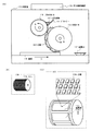
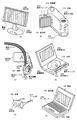
なお、本明細書中でいう印刷法とは、凸版印刷、凹版印刷又はスクリーン印刷などの印刷手段を用いて電極上にEL層を形成する方法のことをいうが、特に凸版印刷を用いてEL層を形成する方法が好ましい。ここで本発明において凸版印刷を用いた印刷法(凸版印刷法)について図1で説明する。
【0022】
図1に示したのは、本発明において凸版印刷法によりEL層の形成を行うための処理室を示す。なお、本明細書中では、EL層を印刷法により形成するための印刷用装置が設置された処理室を印刷室118という。
【0023】
図1において、110はアニロックスロール、111はドクターバー(ドクターブレードともいう)であり、ドクターバー111によりEL材料と溶媒との混合物(以下、EL形成物という)112がアニロックスロール110の表面付近に溜められている。なお、ここでいうEL材料とは蛍光性有機化合物であり、一般的に正孔注入層、正孔輸送層、発光層、電子輸送層もしくは電子注入層と呼ばれている有機化合物を指す。
【0024】
アニロックスロール110の表面には図1(B)に示すようにメッシュ状の溝(以下、メッシュという)110aが設けられており、矢印Aの方向に回転することでメッシュ110aがEL形成物112を表面に保持していく。なお、アニロックスロール110の表面に図示された点線はEL形成物が保持されていることを意味している。
【0025】
そして、113は印刷ロール、114は凸版であり、凸版114はエッチング等により表面に凹凸が形成されている。この様子を図1(C)に示す。図1(C)の場合、1枚の基板上に複数枚の発光装置を作製するために凸版114には画素部用パターン114aが複数箇所に形成されている。さらに、画素部用パターン114aを拡大すると、複数の画素に対応する位置に凸部114bが形成されている。
【0026】
前述のアニロックスロール110は回転しながらメッシュ110aにEL形成物112を保持し続ける。一方、印刷ロール113は矢印Bの方向に回転し、凸版114の凸部114bのみがメッシュ110aと接触する。この時、凸部114bの表面にEL形成物112が塗布される。
【0027】
そして、印刷ロール113と同じ速度で水平移動(矢印Cの方向)する基板115と凸部114bが接した箇所にEL形成物112が印刷される。これにより基板115上にはEL形成物112がマトリクス状に配列された状態で印刷されることになる。
【0028】
その後、別の処理室(本明細書中では、乾燥室という)において大気圧の窒素雰囲気下で加熱処理を行うことによりEL形成物112に含まれる溶媒を気化させてEL材料を残す。このため、溶媒はEL材料のガラス転移温度(Tg)よりも低い温度で気化するものを用いる必要がある。また、EL形成物の粘度により最終的に形成されるEL層の膜厚が決まる。この場合、溶媒の選定により粘度を調節することができるが、粘度は1×10⁻³〜5×10⁻²Pa・s(好ましくは1×10⁻³〜2×10⁻²Pa・s)とするのが好ましい。
【0029】
なお、EL材料を溶解させる代表的な溶媒としてはトルエン、キシレン、クロロベンゼン、ジクロロベンゼン、アニソール、クロロフォルム、ジクロロメタン、γブチルラクトン、ブチルセルソルブ、シクロヘキサン、NMP(N−メチル−2−ピロリドン)、シクロヘキサノン、ジオキサンまたは、THF(テトラヒドロフラン)が挙げられる。
【0030】
さらに、EL形成物112中に結晶核となりうる不純物が多いと、溶媒を気化させる際にEL材料が結晶化してしまう可能性が高くなる。結晶化してしまうと発光効率が落ちるため好ましくなく、できるだけEL形成物112の中には不純物が含まれないようにすることが望ましい。
【0031】
不純物を低減するには、溶媒の精製時、EL材料の精製時、又は溶媒とEL材料を混合する時の環境を可能な限り清浄化しておくことも重要であるが、本発明においては、EL形成物を印刷する際の印刷用装置の雰囲気にも注意することが好ましい。
【0032】
すなわち、上記EL形成物を印刷する際には、印刷用装置が設置された室内(代表的にはクリーンブース内)を窒素、ヘリウム、アルゴンといった不活性気体を充填したり、EL材料を溶解させる溶媒雰囲気にしたりすることが必要である。
【0033】
また、印刷室118内を溶媒雰囲気にする場合には、印刷室118内に備えられている溶媒トレー117に溶媒を備えることで、室内を溶媒雰囲気にすることができる。
【0034】
なお、本発明において不活性気体を充填したり、溶媒雰囲気とした印刷室118内は印刷室118に設けられた圧力調節機構116により、大気圧状態もしくは大気圧に近い状態(典型的には1〜2気圧、好ましくは1.1〜1.5気圧)に保持される。
【0035】
本発明を実施した場合、EL材料を成膜するにあたって真空蒸着装置のような真空排気設備を必要とする装置を必要としないため、設備が簡易になるとともにメンテナンスも容易なものとなる利点がある。
【0036】
なお、本発明はアクティブマトリクス型発光装置にもパッシブマトリクス型(単純マトリクス型)発光装置にも実施することができる。
【0037】
【発明の実施の形態】
次に、印刷によるEL層の形成から電極形成及び封止構造までの一連の処理を行う本発明の装置について図2により説明する。なお、図2に示したのはマルチチャンバー方式の成膜装置の上面図である。
【0038】
図2において、201は搬送室であり、搬送室201には搬送機構202が備えられ、基板203の搬送が行われる。搬送室201は減圧雰囲気にされており、各処理室とはゲートによって連結されている。各処理室への基板の受け渡しは、ゲートを開けた際に搬送機構202によって行われる。また、搬送室201を減圧するには、油回転ポンプ、メカニカルブースターポンプ、ターボ分子ポンプ若しくはクライオポンプなどの排気ポンプを用いることが可能であるが、水分の除去に効果的なクライオポンプが好ましい。
【0039】
以下に、各処理室についての説明を行う。なお、搬送室201は大気雰囲気となるので、搬送室201に直接的に連結された処理室には全て排気ポンプ(図示せず)が備えられている。排気ポンプとしては上述の油回転ポンプ、メカニカルブースターポンプ、ターボ分子ポンプ若しくはクライオポンプが用いられる。
【0040】
まず、204は基板のセッティング(設置)を行うロード室であり、アンロード室も兼ねている。ロード室204はゲート200aにより搬送室201と連結され、ここに基板203をセットしたキャリア(図示せず)が配置される。なお、ロード室204は基板搬入用と基板搬出用とで部屋が区別されていても良い。また、ロード室204は上述の排気ポンプと高純度の窒素ガスまたは希ガスを導入するためのパージラインを備えている。
【0041】
次に、205は印刷法によりEL材料を成膜するための印刷室である。印刷室205はゲート200bを介して搬送室201に連結される。なお、印刷室205内の印刷部206において、正孔注入層、赤色に発色する発光層、緑色に発色する発光層、青色に発色する発光層を成膜することができる。なお、正孔注入層、赤色に発色する発光層、緑色に発色する発光層及び青色に発色する発光層としては如何なる材料を用いても良い。
【0042】
本発明ではEL層の形成方法として印刷法を用いるため、EL材料としてはポリマー系材料を用いるとよい。代表的なポリマー系材料としては、ポリパラフェニレンビニレン(PPV)系、ポリビニルカルバゾール(PVK)系、ポリフルオレン(PF)系などの高分子材料が挙げられる。
【0043】
ポリマー系材料でなる正孔注入層、正孔輸送層又は発光層を印刷法で形成するには、ポリマー前駆体の状態で印刷し、それを加熱することによりポリマー系材料でなるEL材料に転化する。そして、その上に蒸着法等で必要なEL材料を積層して積層型のEL層を形成する。
【0044】
具体的には、正孔輸送層としては、ポリマー前駆体であるポリテトラヒドロチオフェニルフェニレンを用い、加熱によりポリフェニレンビニレンとすることが好ましい。膜厚は30〜100nm(好ましくは40〜80nm)とすれば良い。また、発光層としては、赤色発光層にはシアノポリフェニレンビニレン、緑色発光層にはポリフェニレンビニレン、青色発光層にはポリフェニレンビニレン若しくはポリアルキルフェニレンが好ましい。膜厚は30〜150nm(好ましくは40〜100nm)とすれば良い。
【0045】
また、電極とその上に形成されるEL材料との間に銅フタロシアニンをバッファ層として設けることも有効である。
【0046】
但し、以上の例は本発明のEL材料として用いることのできる材料の一例であって、これに限定する必要はまったくない。本発明ではEL材料と溶媒との混合物を印刷して、溶媒を気化させて除去することによりEL層を形成する。従って、溶媒を気化させる際にEL層のガラス転移温度を超えない組み合わせであれば如何なるEL材料を用いても良い。
【0047】
また、EL形成物の粘度を上げるための添加剤を加えることも有効である。さらに、EL材料としては、溶媒に可溶なものであれば、低分子材料を用いることも可能である。
【0048】
また、EL層を印刷により形成する際、EL層は水分や酸素の存在によって容易に劣化してしまうため、形成する際は極力このような要因を排除しておく必要がある。そのためには、印刷用装置を窒素、アルゴン、ヘリウムといった不活性気体を充填した室内(本実施例では印刷室内)に設置し、その雰囲気中で印刷を行うことが望ましい。
【0049】
なお、このとき用いる不活性気体の露点は、−20度以下であることが好ましいが、さらに好ましくは−50度以下であるとよい。
【0050】
また、EL形成物を均一に成膜する上では、印刷室内をEL形成物を形成する溶媒雰囲気にしておくことも有効である。なお、溶媒雰囲気は、溶媒トレー216に溶媒を備えておくことで形成することができる。
【0051】
この際、不活性気体もしくは、溶媒を充填した室内は大気圧状態もしくは加圧状態(典型的には1〜2気圧、好ましくは1.1〜1.5気圧)に保持しておけば良い。なお、圧力の調節は、圧力調節機構215により行う。本発明を実施した場合、EL材料を成膜するにあたって真空蒸着装置のような真空排気設備を必要とする装置を必要としないため、設備が簡易になるとともにメンテナンスも容易なものとなる利点がある。
【0052】
つぎに、乾燥室207で、印刷室205で成膜したEL材料を乾燥させる。なお、乾燥室207は、ゲート200cを介して搬送室201に連結される。乾燥室207に設けられたホットプレート部208上に基板を載せることで基板上のEL材料を乾燥させることができる。
【0053】
次に、209は蒸着法によりEL素子の陽極もしくは陰極となる導電膜を成膜するための蒸着室である。
【0054】
蒸着室209はゲート200dを介して搬送室201に連結される。
なお、具体的には蒸着室209内の成膜部210において、EL素子の陰極となる導電膜としてMgAgやAl−Li合金膜(アルミニウムとリチウムとの合金膜)といった膜を成膜することができる。
【0055】
なお、周期表の1族もしくは2族に属する元素とアルミニウムとを共蒸着することも可能である。共蒸着とは、同時に蒸着セルを加熱し、成膜段階で異なる物質を混合する蒸着法をいう。
【0056】
次に、211は封止室(封入室またはグローブボックスともいう)であり、ゲート200eを介してロード室204に連結されている。封止室211では、最終的にEL素子を密閉空間に封入するための処理が行われる。この処理は形成されたEL素子を酸素や水分から保護するための処理であり、シーリング材で機械的に封入する、又は熱硬化性樹脂若しくは紫外光硬化性樹脂で封入するといった手段を用いる。
【0057】
シーリング材としては、ガラス、セラミックス、プラスチックもしくは金属を用いることができるが、シーリング材側に光を放射させる場合は透光性でなければならない。また、シーリング材と上記EL素子が形成された基板とは熱硬化性樹脂又は紫外光硬化性樹脂を用いて貼り合わせられ、熱処理又は紫外光照射処理によって樹脂を硬化させて密閉空間を形成する。この密閉空間の中に酸化バリウムに代表される吸湿材を設けることも有効である。
【0058】
また、シーリング材とEL素子の形成された基板との空間を熱硬化性樹脂若しくは紫外光硬化性樹脂で充填することも可能である。この場合、熱硬化性樹脂若しくは紫外光硬化性樹脂の中に酸化バリウムに代表される吸湿材を添加しておくことは有効である。
【0059】
図2に示した成膜装置では、封止室211の内部に紫外光を照射するための機構(以下、紫外光照射機構という)212が設けられており、この紫外光照射機構212から発した紫外光によって紫外光硬化性樹脂を硬化させる構成となっている。また、封止室211の内部は排気ポンプを取り付けることで減圧とすることも可能である。上記封入工程をロボット操作で機械的に行う場合には、減圧下で行うことで酸素や水分の混入を防ぐことができる。また、逆に封止室211の内部を与圧とすることも可能である。この場合、高純度な窒素ガスや希ガスでパージしつつ与圧とし、外気から酸素等が侵入することを防ぐ。
【0060】
次に、封止室211には受渡室(パスボックス)213が連結される。受渡室213には搬送機構(B)214が設けられ、封止室211でEL素子の封入が完了した基板を受渡室213へと搬送する。受渡室213も排気ポンプを取り付けることで減圧とすることが可能である。この受渡室213は封止室211を直接外気に晒さないようにするための設備であり、ここから基板を取り出す。
【0061】
以上のような成膜装置を用いることでEL素子を密閉空間に封入するまでの一連の処理を外気に晒さずに済むため、信頼性の高い発光装置を作製することが可能となる。しかし、ここで示した成膜装置は、本発明における実施の形態の一つであり、本発明を限定するものではない。
【0062】
【実施例】
〔実施例1〕
ここでは、本発明を実施して同一基板上に画素部と、画素部の周辺に設ける駆動回路のTFT(nチャネル型TFT及びpチャネル型TFT)を同時に作製する方法について詳細に図3〜図5を用いて説明する。
【0063】
まず、本実施例ではコーニング社の#7059ガラスや#1737ガラスなどに代表されるバリウムホウケイ酸ガラス、またはアルミノホウケイ酸ガラスなどのガラスからなる基板300を用いる。なお、基板300としては、透光性を有する基板であれば限定されず、石英基板を用いても良い。また、本実施例の処理温度に耐えうる耐熱性を有するプラスチック基板を用いてもよい。
【0064】
次いで、基板300上に酸化珪素膜、窒化珪素膜または酸化窒化珪素膜などの絶縁膜から成る下地膜301を形成する。本実施例では下地膜301として2層構造を用いるが、前記絶縁膜の単層膜または2層以上積層させた構造を用いても良い。下地膜301の一層目としては、プラズマCVD法を用い、SiH4、NH3、及びN2Oを反応ガスとして成膜される酸化窒化珪素膜301aを10〜200nm(好ましくは50〜100nm)形成する。本実施例では、膜厚50nmの酸化窒化珪素膜301a(組成比Si=32%、O=27%、N=24%、H=17%)を形成した。次いで、下地膜301のニ層目としては、プラズマCVD法を用い、SiH4、及びN2Oを反応ガスとして成膜される酸化窒化珪素膜301bを50〜200nm(好ましくは100〜150nm)の厚さに積層形成する。本実施例では、膜厚100nmの酸化窒化珪素膜301b(組成比Si=32%、O=59%、N=7%、H=2%)を形成した。
【0065】
次いで、下地膜上に半導体層302〜305を形成する。半導体層302〜305は、非晶質構造を有する半導体膜を公知の手段(スパッタ法、LPCVD法、またはプラズマCVD法等)により成膜した後、公知の結晶化処理(レーザー結晶化法、熱結晶化法、またはニッケルなどの触媒を用いた熱結晶化法等)を行って得られた結晶質半導体膜を所望の形状にパターニングして形成する。この半導体層302〜305の厚さは25〜80nm(好ましくは30〜60nm)の厚さで形成する。結晶質半導体膜の材料に限定はないが、好ましくは珪素(シリコン)またはシリコンゲルマニウム(SiXGe1-X(X=0.0001〜0.02))合金などで形成すると良い。本実施例では、プラズマCVD法を用い、55nmの非晶質珪素膜を成膜した後、ニッケルを含む溶液を非晶質珪素膜上に保持させた。この非晶質珪素膜に脱水素化(500℃、1時間)を行った後、熱結晶化(550℃、4時間)を行い、さらに結晶化を改善するためのレーザーアニ―ル処理を行って結晶質珪素膜を形成した。そして、この結晶質珪素膜をフォトリソグラフィ法を用いたパターニング処理によって、半導体層302〜305を形成した。
【0066】
また、半導体層302〜305を形成した後、TFTのしきい値を制御するために微量な不純物元素(ボロンまたはリン)のドーピングを行ってもよい。
【0067】
また、レーザー結晶化法で結晶質半導体膜を作製する場合には、パルス発振型または連続発光型のエキシマレーザーやYAGレーザー、YVO4レーザーを用いることができる。これらのレーザーを用いる場合には、レーザー発振器から放射されたレーザー光を光学系で線状に集光し半導体膜に照射する方法を用いると良い。結晶化の条件は実施者が適宣選択するものであるが、エキシマレーザーを用いる場合はパルス発振周波数300Hzとし、レーザーエネルギー密度を100〜400mJ/cm2(代表的には200〜300mJ/cm2)とする。また、YAGレーザーを用いる場合にはその第2高調波を用いパルス発振周波数30〜300Hzとし、レーザーエネルギー密度を300〜600mJ/cm2(代表的には350〜500mJ/cm2)とすると良い。そして幅100〜1000μm、例えば400μmで線状に集光したレーザー光を基板全面に渡って照射し、この時の線状レーザー光の重ね合わせ率(オーバーラップ率)を50〜90%として行えばよい。
【0068】
次いで、半導体層302〜305を覆うゲート絶縁膜306を形成する。ゲート絶縁膜306はプラズマCVD法またはスパッタ法を用い、厚さを40〜150nmとして珪素を含む絶縁膜で形成する。本実施例では、プラズマCVD法により110nmの厚さで酸化窒化珪素膜(組成比Si=32%、O=59%、N=7%、H=2%)で形成した。勿論、ゲート絶縁膜は酸化窒化珪素膜に限定されるものでなく、他の珪素を含む絶縁膜を単層または積層構造として用いても良い。
【0069】
また、酸化珪素膜を用いる場合には、プラズマCVD法でTEOS(Tetraethyl Orthosilicate)とO2とを混合し、反応圧力40Pa、基板温度300〜400℃とし、高周波(13.56MHz)電力密度0.5〜0.8W/cm2で放電させて形成することができる。このようにして作製される酸化珪素膜は、その後400〜500℃の熱アニールによりゲート絶縁膜として良好な特性を得ることができる。
【0070】
次いで、図3(A)に示すように、ゲート絶縁膜306上に膜厚20〜100nmの第1の導電膜307と、膜厚100〜400nmの第2の導電膜308とを積層形成する。本実施例では、膜厚30nmのTaN膜からなる第1の導電膜307と、膜厚370nmのW膜からなる第2の導電膜308を積層形成した。TaN膜はスパッタ法で形成し、Taのターゲットを用い、窒素を含む雰囲気内でスパッタした。また、W膜は、Wのターゲットを用いたスパッタ法で形成した。その他に6フッ化タングステン(WF6)を用いる熱CVD法で形成することもできる。いずれにしてもゲート電極として使用するためには低抵抗化を図る必要があり、W膜の抵抗率は20μΩcm以下にすることが望ましい。W膜は結晶粒を大きくすることで低抵抗率化を図ることができるが、W膜中に酸素などの不純物元素が多い場合には結晶化が阻害され高抵抗化する。従って、本実施例では、高純度のW(純度99.9999%)のターゲットを用いたスパッタ法で、さらに成膜時に気相中からの不純物の混入がないように十分配慮してW膜を形成することにより、抵抗率9〜20μΩcmを実現することができた。
【0071】
なお、本実施例では、第1の導電膜307をTaN、第2の導電膜308をWとしたが、特に限定されず、いずれもTa、W、Ti、Mo、Al、Cu、Cr、Ndから選ばれた元素、または前記元素を主成分とする合金材料若しくは化合物材料で形成してもよい。また、リン等の不純物元素をドーピングした多結晶珪素膜に代表される半導体膜を用いてもよい。また、Ag、Pd、Cuからなる合金を用いてもよい。また、第1の導電膜をタンタル(Ta)膜で形成し、第2の導電膜をW膜とする組み合わせ、第1の導電膜を窒化チタン(TiN)膜で形成し、第2の導電膜をW膜とする組み合わせ、第1の導電膜を窒化タンタル(TaN)膜で形成し、第2の導電膜をAl膜とする組み合わせ、第1の導電膜を窒化タンタル(TaN)膜で形成し、第2の導電膜をCu膜とする組み合わせとしてもよい。
【0072】
次に、図3(B)に示すようにフォトリソグラフィ法を用いてレジストからなるマスク309〜313を形成し、電極及び配線を形成するための第1のエッチング処理を行う。第1のエッチング処理では第1及び第2のエッチング条件で行う。本実施例では第1のエッチング条件として、ICP(Inductively Coupled Plasma:誘導結合型プラズマ)エッチング法を用い、エッチング用ガスにCF4とCl2とO2とを用い、それぞれのガス流量比を25/25/10(sccm)とし、1Paの圧力でコイル型の電極に500WのRF(13.56MHz)電力を投入してプラズマを生成してエッチングを行った。ここでは、松下電器産業(株)製のICPを用いたドライエッチング装置(Model E645−□ICP)を用いた。基板側(試料ステージ)にも150WのRF(13.56MHz)電力を投入し、実質的に負の自己バイアス電圧を印加する。この第1のエッチング条件によりW膜をエッチングして第1の導電層の端部をテーパー形状とする。第1のエッチング条件でのWに対するエッチング速度は200.39nm/min、TaNに対するエッチング速度は80.32nm/minであり、TaNに対するWの選択比は約2.5である。また、この第1のエッチング条件によって、Wのテーパー角は、約26°となる。
【0073】
この後、図3(B)に示すようにレジストからなるマスク309〜313を除去せずに第2のエッチング条件に変え、エッチング用ガスにCF4とCl2とを用い、それぞれのガス流量比を30/30(sccm)とし、1Paの圧力でコイル型の電極に500WのRF(13.56MHz)電力を投入してプラズマを生成して約30秒程度のエッチングを行った。基板側(試料ステージ)にも20WのRF(13.56MHz)電力を投入し、実質的に負の自己バイアス電圧を印加する。CF4とCl2を混合した第2のエッチング条件ではW膜及びTaN膜とも同程度にエッチングされる。第2のエッチング条件でのWに対するエッチング速度は58.97nm/min、TaNに対するエッチング速度は66.43nm/minである。なお、ゲート絶縁膜上に残渣を残すことなくエッチングするためには、10〜20%程度の割合でエッチング時間を増加させると良い。
【0074】
上記第1のエッチング処理では、レジストからなるマスクの形状を適したものとすることにより、基板側に印加するバイアス電圧の効果により第1の導電層及び第2の導電層の端部がテーパー形状となる。このテーパー部の角度は15〜45°とすればよい。こうして、第1のエッチング処理により第1の導電層と第2の導電層から成る第1の形状の導電層314〜318(第1の導電層314a〜318aと第2の導電層314b〜318b)を形成する。ここでのチャネル長方向の第1の導電層の幅は、上記実施の形態に示したW1に相当する。319はゲート絶縁膜であり、第1の形状の導電層314〜318で覆われない領域は20〜50nm程度エッチングされ薄くなった領域が形成される。
【0075】
そして、レジストからなるマスクを除去せずに第1のドーピング処理を行い、半導体層にn型を付与する不純物元素を添加する。(図3(B))ドーピング処理はイオンドープ法、若しくはイオン注入法で行えば良い。イオンドープ法の条件はドーズ量を1×10¹³〜5×10¹⁵atoms/cm2とし、加速電圧を60〜100keVとして行う。本実施例ではドーズ量を1.5×1015atoms/cm2とし、加速電圧を80keVとして行った。n型を付与する不純物元素として15族に属する元素、典型的にはリン(P)または砒素(As)を用いるが、ここではリン(P)を用いた。この場合、導電層314〜318がn型を付与する不純物元素に対するマスクとなり、自己整合的に高濃度不純物領域320〜323が形成される。高濃度不純物領域320〜323には1×1020〜1×1021atoms/cm3の濃度範囲でn型を付与する不純物元素を添加する。
【0076】
次いで、図3(C)に示すようにレジストからなるマスクを除去せずに第2のエッチング処理を行う。ここでは、エッチング用ガスにCF4とCl2とO2とを用い、それぞれのガス流量比を25/25/10(sccm)とし、1Paの圧力でコイル型の電極に500WのRF(13.56MHz)電力を投入してプラズマを生成してエッチングを行った。基板側(試料ステージ)にも20WのRF(13.56MHz)電力を投入し、実質的に負の自己バイアス電圧を印加する。第2のエッチング処理でのWに対するエッチング速度は124.62nm/min、TaNに対するエッチング速度は20.67nm/minであり、TaNに対するWの選択比は6.05である。従って、W膜が選択的にエッチングされる。この第2のエッチングによりWのテーパー角は70°となった。この第2のエッチング処理により第2の導電層324b〜327bを形成する。一方、第1の導電層314a〜318aは、ほとんどエッチングされず、第1の導電層324a〜327aを形成する。
【0077】
次いで、第2のドーピング処理を行う。ドーピングは第2の導電層324b〜328bを不純物元素に対するマスクとして用い、第1の導電層のテーパー部下方に形成されている半導体層に不純物元素が添加されるようにドーピングする。本実施例では、不純物元素としてP(リン)を用い、ドーズ量3.5×10¹²atoms/cm3、加速電圧90keVにてプラズマドーピングを行った。こうして、第1の導電層と重なる低濃度不純物領域329〜332を自己整合的に形成する。この低濃度不純物領域329〜332へ添加されたリン(P)の濃度は、1×1017〜1×1018atoms/cm3であり、且つ、第1の導電層のテーパー部における膜厚に従って緩やかな濃度勾配を有している。なお、第1の導電層のテーパー部と重なる半導体層において、第1の導電層のテーパー部の端部から内側に向かって若干、不純物濃度が低くなっているものの、ほぼ同程度の濃度である。また、高濃度不純物領域333〜336にも不純物元素が添加され、高濃度不純物領域333〜336を形成する。
【0078】
次いで、図4(A)に示すようにレジストからなるマスクを除去せずに第3のエッチング処理を行う。この第3のエッチング処理では第1の導電層のテーパー部を部分的にエッチングして、半導体層と重なる領域を縮小するために行われる。第3のエッチング処理は、エッチングガスにCHF3を用い、反応性イオンエッチング法(RIE法)を用いて行う。本実施例では、チャンバー圧力6.7Pa、RF電力800W、CHF3ガス流量35sccmで第3のエッチング処理を行った。第3のエッチングにより、第1の導電層341〜344が形成される。
【0079】
この第3のエッチング処理時、同時に絶縁膜319もエッチングされて、高濃度不純物領域333〜336の一部は露呈し、絶縁膜346a〜346dが形成される。なお、本実施例では、高濃度不純物領域333〜336の一部が露呈するエッチング条件を用いたが、絶縁膜の膜厚やエッチング条件を変更すれば、高濃度不純物領域に薄く絶縁膜が残るようにすることもできる。
【0080】
上記第3のエッチングによって、第1の導電層341〜344と重ならない不純物領域(LDD領域)337a〜340aが形成される。なお、不純物領域(GOLD領域)337b〜340bは、第1の導電層341〜344と重なったままである。
【0081】
また、第1の導電層341と第2の導電層324bとで形成された電極は、後の工程で形成される駆動回路のnチャネル型TFTのゲート電極となり、第1の導電層342と第2の導電層325bとで形成された電極は、後の工程で形成される駆動回路のpチャネル型TFTのゲート電極となる。同様に、第1の導電層343と第2の導電層326bとで形成された電極は、後の工程で形成される画素部のnチャネル型TFTのゲート電極となり、第1の導電層344と第2の導電層327bとで形成された電極は、後の工程で形成される画素部のnチャネル型TFTのゲート電極となる。
【0082】
このようにして、本実施例は、第1の導電層341〜344と重なる不純物領域(GOLD領域)337b〜340bにおける不純物濃度と、第1の導電層341〜344と重ならない不純物領域(LDD領域)337a〜340aにおける不純物濃度との差を小さくすることができ、TFT特性を向上させることができる。
【0083】
次いで、レジストからなるマスクを除去した後、新たにレジストからなるマスク348、349を形成して第3のドーピング処理を行う。この第3のドーピング処理により、pチャネル型TFTの活性層となる半導体層に前記一導電型(n型)とは逆の導電型(p型)を付与する不純物元素が添加された不純物領域350〜355を形成する。(図4(B))第1の導電層342、344を不純物元素に対するマスクとして用い、p型を付与する不純物元素を添加して自己整合的に不純物領域を形成する。本実施例では、不純物領域350〜355はジボラン(B2H6)を用いたイオンドープ法で形成する。なお、この第3のドーピング処理の際には、nチャネル型TFTを形成する半導体層はレジストからなるマスク348、349で覆われている。第1のドーピング処理及び第2のドーピング処理によって、不純物領域348、349にはそれぞれ異なる濃度でリンが添加されているが、そのいずれの領域においてもp型を付与する不純物元素の濃度が2×10²⁰〜2×10²¹atoms/cm3となるようにドーピング処理することにより、pチャネル型TFTのソース領域およびドレイン領域として機能するために何ら問題は生じない。本実施例では、第3のエッチング処置によって、pチャネル型TFTの活性層となる半導体層の一部が露呈されたため、不純物元素(ボロン)を添加しやすい利点を有している。
【0084】
以上までの工程でそれぞれの半導体層に不純物領域が形成される。
【0085】
次いで、レジストからなるマスク348、349を除去して第1の層間絶縁膜356を形成する。この第1の層間絶縁膜356としては、プラズマCVD法またはスパッタ法を用い、厚さを100〜200nmとして珪素を含む絶縁膜で形成する。本実施例では、プラズマCVD法により膜厚150nmの酸化窒化珪素膜を形成した。勿論、第1の層間絶縁膜356は酸化窒化珪素膜に限定されるものでなく、他の珪素を含む絶縁膜を単層または積層構造として用いても良い。
【0086】
次いで、図4(C)に示すように、それぞれの半導体層に添加された不純物元素を活性化処理する工程を行う。この活性化工程はファーネスアニール炉を用いる熱アニール法で行う。熱アニール法としては、酸素濃度が1ppm以下、好ましくは0.1ppm以下の窒素雰囲気中で400〜700℃、代表的には500〜550℃で行えばよく、本実施例では550℃、4時間の熱処理で活性化処理を行った。なお、熱アニール法の他に、レーザーアニール法、またはラピッドサーマルアニール法(RTA法)を適用することができる。
【0087】
なお、本実施例では、上記活性化処理と同時に、結晶化の際に触媒として使用したニッケルが高濃度のリンを含む不純物領域(333、335、350、353)にゲッタリングされ、主にチャネル形成領域となる半導体層中のニッケル濃度が低減される。このようにして作製したチャネル形成領域を有するTFTはオフ電流値が下がり、結晶性が良いことから高い電界効果移動度が得られ、良好な特性を達成することができる。
【0088】
また、第1の層間絶縁膜を形成する前に活性化処理を行っても良い。ただし、用いた配線材料が熱に弱い場合には、本実施例のように配線等を保護するため層間絶縁膜(シリコンを主成分とする絶縁膜、例えば窒化珪素膜)を形成した後で活性化処理を行うことが好ましい。
【0089】
さらに、3〜100%の水素を含む雰囲気中で、300〜550℃で1〜12時間の熱処理を行い、半導体層を水素化する工程を行う。本実施例では水素を約3%の含む窒素雰囲気中で410℃、1時間の熱処理を行った。この工程は層間絶縁膜に含まれる水素により半導体層のダングリングボンドを終端する工程である。水素化の他の手段として、プラズマ水素化(プラズマにより励起された水素を用いる)を行っても良い。
【0090】
また、活性化処理としてレーザーアニール法を用いる場合には、上記水素化を行った後、エキシマレーザーやYAGレーザー等のレーザー光を照射することが望ましい。
【0091】
次いで、図5(A)に示すように第1の層間絶縁膜356上に有機絶縁物材料から成る第2の層間絶縁膜357を形成する。本実施例では膜厚1.6μmのアクリル樹脂膜を形成した。次いで、各不純物領域333、335、350、353に達するコンタクトホールを形成するためのパターニングを行う。
【0092】
第2の層間絶縁膜357としては、珪素を含む絶縁材料や有機樹脂からなる膜を用いる。珪素を含む絶縁材料としては、酸化珪素、窒化珪素、酸化窒化珪素を用いることができ、また有機樹脂としては、ポリイミド、ポリアミド、アクリル、BCB(ベンゾシクロブテン)などを用いることができる。
【0093】
本実施例では、プラズマCVD法により形成された酸化窒化珪素膜を形成した。なお、酸化窒化珪素膜の膜厚として好ましくは1〜5μm(さらに好ましくは2〜4μm)とすればよい。酸化窒化珪素膜は、膜自身に含まれる水分が少ないためにEL素子の劣化を抑える上で有効である。また、コンタクトホールの形成には、ドライエッチングまたはウエットエッチングを用いることができるが、エッチング時における静電破壊の問題を考えると、ウエットエッチング法を用いるのが望ましい。
【0094】
さらに、ここでのコンタクトホールの形成において、第1層間絶縁膜356及び第2層間絶縁膜357を同時にエッチングするため、コンタクトホールの形状を考えると第2層間絶縁膜357を形成する材料は、第1層間絶縁膜356を形成する材料よりもエッチング速度の速いものを用いるのが好ましい。
【0095】
そして、各不純物領域333、335、350、353とそれぞれ電気的に接続する配線358〜365を形成する。そして、膜厚50nmのTi膜と、膜厚500nmの合金膜(AlとTiとの合金膜)との積層膜をパターニングして形成するが、他の導電膜を用いても良い。
【0096】
次いで、その上に透明導電膜を80〜120nmの厚さで形成し、パターニングすることによって陽極367を形成する。(図5(A))なお、本実施例では、陽極として酸化インジウム・スズ(ITO)膜や酸化インジウムに2〜20[%]の酸化亜鉛(ZnO)を混合した透明導電膜を用いる。
【0097】
また、陽極367は、ドレイン配線365と接して重ねて形成することによって電流制御用TFT404のドレイン領域と電気的な接続が形成される。
【0098】
次に、図5(B)に示すように、珪素を含む絶縁膜(本実施例では酸化珪素膜)を500[nm]の厚さに形成し、陽極367に対応する位置に開口部を形成して、バンクとして機能する第3の層間絶縁膜368を形成する。開口部を形成する際、ウエットエッチング法を用いることで容易にテーパー形状の側壁とすることができる。開口部の側壁が十分になだらかでないと段差に起因するEL層の劣化が顕著な問題となってしまうため、注意が必要である。
【0099】
なお、本実施例においては、第3の層間絶縁膜368として酸化珪素でなる膜を用いているが、場合によっては、ポリイミド、ポリアミド、アクリル、BCB(ベンゾシクロブテン)といった有機樹脂膜を用いることもできる。
【0100】
次に、図2で説明したマルチチャンバー方式の成膜装置を用いて、図5(B)で示すようにEL層369を凸版印刷法により形成し、更に蒸着法により陰極(MgAg電極)370および保護電極を形成する。このときEL層369及び陰極370を形成するに先立って陽極367に対して熱処理を施し、水分を完全に除去しておくことが望ましい。なお、本実施例ではEL素子の陰極としてMgAg電極を用いるが、公知の他の材料であっても良い。
【0101】
なお、EL層369として【発明の実施の形態】の欄で説明した材料を用いることができる。本実施例では正孔輸送層(Hole transporting layer)及び発光層(Emitting layer)でなる2層構造をEL層とするが、正孔注入層、電子注入層若しくは電子輸送層のいずれかを設ける場合もある。このように組み合わせは既に様々な例が報告されており、そのいずれの構成を用いても構わない。
【0102】
本実施例では正孔輸送層としてポリマー前駆体であるポリテトラヒドロチオフェニルフェニレンを印刷法により形成し、加熱によりポリフェニレンビニレンとする。また、発光層としては、ポリビニルカルバゾールに1,3,4−オキサジアゾール誘導体のPBDを30〜40%分子分散させたものを蒸着法により形成し、緑色の発光中心としてクマリン6を約1%添加している。
【0103】
また、保護電極371でもEL層369を水分や酸素から保護することは可能であるが、さらに好ましくはパッシベーション膜372を設けると良い。本実施例ではパッシベーション膜372として300nm厚の窒化珪素膜を設ける。このパッシベーション膜も保護電極371の後に大気解放しないで連続的に形成しても構わない。
【0104】
また、保護電極371は陰極370の劣化を防ぐために設けられ、アルミニウムを主成分とする金属膜が代表的である。勿論、他の材料でも良い。また、EL層369、陰極370は非常に水分に弱いので、保護電極371までを大気解放しないで連続的に形成し、外気からEL層を保護することが望ましい。
【0105】
なお、EL層369の膜厚は10〜400[nm](典型的には60〜150[nm])、陰極370の厚さは80〜200[nm](典型的には100〜150[nm])とすれば良い。
【0106】
こうして図5(B)に示すような構造のELモジュールが完成する。なお、本実施例におけるELモジュールの作成工程においては、回路の構成および工程の関係上、ゲート電極を形成している材料であるTa、Wによってソース信号線を形成し、ソース、ドレイン電極を形成している配線材料であるAlによってゲート信号線を形成しているが、異なる材料を用いても良い。
【0107】
また、nチャネル型TFT401及びpチャネル型TFT402を有する駆動回路406と、スイッチング用TFT403、電流制御用TFT404及び保持容量405とを有する画素部407を同一基板上に形成することができる。
【0108】
駆動回路406のnチャネル型TFT401はチャネル形成領域372、ゲート電極の一部を構成する第1の導電層341と重なる低濃度不純物領域337b(GOLD領域)、ゲート電極の外側に形成される低濃度不純物領域337a(LDD領域)とソース領域またはドレイン領域として機能する高濃度不純物領域333を有している。pチャネル型TFT402にはチャネル形成領域373、ゲート電極の一部を構成する第1の導電層342と重なる不純物領域338b、ゲート電極の外側に形成される不純物領域338a、ソース領域またはドレイン領域として機能する不純物領域334を有している。
【0109】
画素部407のスイッチング用TFT403にはチャネル形成領域374、ゲート電極を形成する第1の導電層343と重なる低濃度不純物領域339b(GOLD領域)、ゲート電極の外側に形成される低濃度不純物領域339a(LDD領域)とソース領域またはドレイン領域として機能する高濃度不純物領域335を有している。電流制御用TFT404にはチャネル形成領域375、ゲート電極を形成する第1の導電層344と重なる低濃度不純物領域355(GOLD領域)、ゲート電極の外側に形成される低濃度不純物領域354(LDD領域)とソース領域またはドレイン領域として機能する高濃度不純物領域353を有している。また、保持容量405は、第一の導電層376aと第二の導電層376bを一方の電極として機能するように形成されている。
【0110】
次に、図5(B)まで作成したELモジュールを発光装置として完成させる方法について図6を用いて説明する。
【0111】
図6(A)は、EL素子の封止までを行った状態を示す上面図、図6(B)は図6(A)をA−A’で切断した断面図である。点線で示された601はソース側駆動回路、602は画素部、603はゲート側駆動回路である。また、604はカバー材、605は第1シール材、606は第2シール材であり、第1シール材605で囲まれた内側には封止材607が設けられる。
【0112】
なお、608はソース側駆動回路601及びゲート側駆動回路603に入力される信号を伝送するための配線であり、外部入力端子となるFPC(フレキシブルプリントサーキット)609からビデオ信号やクロック信号を受け取る。なお、ここではFPCしか図示されていないが、このFPCにはプリント配線基盤(PWB)が取り付けられていても良い。本明細書における発光装置には、発光装置本体だけでなく、それにFPCもしくはPWBが取り付けられた状態をも含むものとする。
【0113】
次に、断面構造について図6(B)を用いて説明する。基板610の上方には画素部602、ゲート側駆動回路603が形成されており、画素部602は電流制御用TFT611とそのドレインに電気的に接続された陽極612を含む複数の画素により形成される。また、ゲート側駆動回路603はnチャネル型TFT613とpチャネル型TFT614とを組み合わせたCMOS回路(図5参照)を用いて形成される。
【0114】
612は陽極である。また、陽極612の両端にはバンク615が形成され、陽極612上にはEL層616およびEL素子の陰極617が形成される。
【0115】
陰極617は全画素に共通の配線としても機能し、接続配線608を経由してFPC609に電気的に接続されている。さらに、画素部602及びゲート側駆動回路603に含まれる素子は全て陰極617およびパッシベーション膜618で覆われている。
【0116】
また、第1シール材605によりカバー材604が貼り合わされている。なお、カバー材604とEL素子との間隔を確保するために樹脂膜からなるスペーサを設けても良い。そして、第1シール材605の内側には封止材607が充填されている。なお、第1シール材605、封止材607としてはエポキシ系樹脂を用いるのが好ましい。また、第1シール材605はできるだけ水分や酸素を透過しない材料であることが望ましい。さらに、封止材607の内部に吸湿効果をもつ物質や酸化を防止する効果をもつ物質を含有させても良い。
【0117】
EL素子を覆うようにして設けられた封止材607はカバー材604を接着するための接着剤としても機能する。また、本実施例ではカバー材604を構成するプラスチック基板の材料としてFRP(Fiberglass-Reinforced Plastics)、PVF(ポリビニルフロライド)、マイラー、ポリエステルまたはアクリルを用いることができる。
【0118】
また、封止材607を用いてカバー材604を接着した後、封止材607の側面(露呈面)を覆うように第2シール材606を設ける。第2シール材606は第1シール材605と同じ材料を用いることができる。
【0119】
以上のような構造でEL素子を封止材607に封入することにより、EL素子を外部から完全に遮断することができ、外部から水分や酸素等のEL層の酸化による劣化を促す物質が侵入することを防ぐことができる。従って、信頼性の高い発光装置を得ることができる。
【0120】
〔実施例2〕
実施例1においては、マルチチャンバー方式の成膜装置を用いてEL層の形成からEL素子の封止まで行う方法を示したが、本実施例では、インライン方式の装置を用いて、EL層の形成からEL素子の封止までの一連の処理を行う方法について図7を用いて説明する。
【0121】
図7(A)は、インライン方式の成膜装置の上面図であり、図7(B)は、その側面図である。701は、処理基板のローダー部(搬送部)である。実施例1で示したように、EL素子の陽極(又は陰極)まで形成した後、ローダー部701に処理基板をセットする。
【0122】
基板は、凸版印刷装置が備えられている印刷室702において、EL層の印刷がなされる。印刷室702は、図7(B)に示すように、インクタンク703、ドクターバー704、アニロックスロール705、印刷ロール706で構成されており、インクタンク703からEL形成物が注入されると、アニロックスロール705にEL形成物が備えられ、さらに印刷ロール706の凸部に塗布される。なお、この時ドクターバー704により、インクタンク703から注入されたEL形成物がアニロックスロール表面に均一に備えられるように調節される。
【0123】
そして、印刷ロール706と同じ速度で水平移動(矢印lの方向)する基板と印刷ロール706の凸部が接した箇所(成膜部709)にEL形成物が印刷される。
【0124】
なお、この時基板はアライメント用に設けられているモニター(図示せず)により位置あわせが行われている。
【0125】
また、印刷室702は、不活性気体もしくは、EL形成物に含まれる溶媒雰囲気下にし、さらに印刷室内は、大気圧状態もしくは、それに近い状態(典型的には、1〜2気圧、好ましくは、1.1〜1.5気圧)に保持しておけばよい。なお、圧力調節は、圧力調節機構707により行う。このとき、溶媒トレー708に溶媒を備えておくことで印刷室内を溶媒雰囲気にすることができる。
【0126】
本実施例では、ポリマー系材料でなる正孔注入層、正孔輸送層又は発光層を印刷法で形成する。はじめに正孔注入層及び正孔輸送層を印刷する。ここでは、ポリチオフェン誘導体であるPEDOT(poly(3,4‐ethylene dioxythiophene))とアクセプター材料となるポリスチレンスルホン酸(PSS)を水に溶かして水溶液にしたものを用いる。そして、乾燥室710において水分を蒸発させることで正孔注入層及び正孔輸送層を形成する。なお、この時基板はホットプレート部711において、80度〜150度で加熱される。
【0127】
次に、発光層として、赤色発光層にはシアノポリフェニレンビニレン、緑色発光層にはポリフェニレンビニレン、青色発光層にはポリフェニレンビニレン若しくはポリアルキルフェニレンをそれぞれ含むEL形成物を印刷室において印刷する。なお、この時の発光層の膜厚は30〜150nm(好ましくは40〜100nm)とすれば良い。
【0128】
そして、EL形成物が印刷された基板を再び乾燥室710にいれ、EL形成物中の溶媒を気化させて、EL材料を残す。なお、乾燥室710には、ホットプレート部711が備えられており、ホットプレート部711上に処理基板を載せて、加熱することにより処理する。また、このときの処理温度は、20〜150℃であることが好ましいが、溶媒の揮発性に合わせて適宜調節すると良い。
【0129】
以上のように正孔注入層、正孔輸送層及び発光層でなるEL層を形成した後、蒸着室712においては、EL素子の陰極(もしくは陽極)となる導電膜を蒸着法により形成することができる。具体的には、蒸着室712の成膜部713においてEL素子の陰極となる導電膜としてMgAgやAl−Li合金膜(アルミニウムとリチウムからなる合金膜)といった膜を成膜することができる。また、蒸着に用いる材料は、蒸着源714に備えられている。
【0130】
なお、蒸着室712は、電極を形成させるためだけに用いるのではなく、EL層の一部を形成させるときに用いることもできる。
【0131】
以上のように、EL素子を形成した後で、封止室715において、最終的にEL素子を密閉空間に封入する処理が行われる。この処理は形成されたEL素子を酸素や水分から保護するための処理であり、シーリング材で機械的に封入する、又は熱硬化性樹脂若しくは紫外光硬化性樹脂で封入するといった手段を用いる。
【0132】
図7に示した成膜装置では、封止室715の内部に紫外光を照射するための機構(以下、紫外光照射機構という)716が設けられており、この紫外光照射機構716から発した紫外光によって成膜部717に備えられた基板上の紫外光硬化性樹脂を硬化させる構成となっている。また、封止室715の内部は排気ポンプを取り付けることで減圧とすることも可能である。上記封入工程をロボット操作で機械的に行う場合には、減圧下で行うことで酸素や水分の混入を防ぐことができる。また、逆に封止室715の内部を与圧とすることも可能である。この場合、高純度な窒素ガスや希ガスでパージしつつ与圧とし、外気から酸素等が侵入することを防ぐ。
【0133】
封止室715において処理された後、基板はアンローダー718へと搬送される。以上により、インライン方式の成膜装置により処理が完了する。なお、本成膜装置は、各処理室ごとに隔離され、各処理に応じた環境にすることができる。また、成膜装置内をEL素子に影響を与えないような水分を含まない不活性気体雰囲気下にしておくと良い。
【0134】
以上のように、図7に示した成膜装置を用いることで完全にEL素子を密閉空間に封入するまで外気に晒さずに済むため、信頼性の高い発光装置を作製することが可能となる。また、インライン方式により高いスループットで発光装置を作製することができる。
【0135】
なお、本実施例の構成は、実施例1の構成とも自由に組み合わせることが可能である。
【0136】
〔実施例3〕
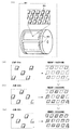
本実施例では、実施例1で示した凸版印刷法により多色のEL層を形成する方法について説明する。図8(A)の801には、印刷室に備えられている印刷ロールを示している。なお、印刷ロール801の表面には、エッチング等により凸版が形成されている。そして、一枚の基板上に複数枚の発光装置を形成させるために凸版には、画素部用パターン802が複数箇所に形成されている。
【0137】
さらに画素部用パターン802を拡大すると複数の画素に対応する位置に凸部803が形成されている。しかし、本実施例においては、複数色を凸版印刷により形成することから、さらに色ごとに異なる形状の凸部803を形成する。
【0138】
例えば、図8(B)に示す凸部803aを用いてEL形成物を印刷すると、1色目の画素部が図8(B)実線領域に示すように形成される。
さらに、図8(C)に示す凸部803bを用いて1色目と異なるEL形成物を印刷すると、1色目と異なる画素部に2色目が図8(C)に示すように形成される。
【0139】
そして、さらに図8(D)に示す凸部803cを用いて1、2色目とは異なるEL形成物を印刷すると、1、2色目と異なる画素部に3色目が図8(D)に示すように形成される。
【0140】
以上により、画素部に3色のEL形成物を印刷することが可能となる。ただし、ここで示したEL形成物の種類は、3色に限られる必要はなく、2色であっても、3色以上であっても良い。
【0141】
また、ここで多色印刷を行う上では、複数の凸部が必要となるが、これは、印刷室を複数設けてもよいし、一つの印刷室で各色ごとに全ての基板を処理した後で、凸部を交換して多色印刷を行っても良い。
【0142】
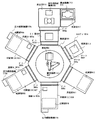
ここで、図9に複数の印刷室を設けたマルチチャンバー方式の成膜装置を示す。図9において、901は搬送室であり、搬送室901には搬送機構(A)902が備えられ、基板903の搬送が行われる。搬送室901は減圧雰囲気にされており、各処理室とはゲートによって連結されている。各処理室への基板の受け渡しは、ゲートを開けた際に搬送機構(A)902によって行われる。
【0143】
また、搬送室901を減圧するには、油回転ポンプ、メカニカルブースターポンプ、ターボ分子ポンプ若しくはクライオポンプなどの排気ポンプを用いることが可能であるが、水分の除去に効果的なクライオポンプが好ましい。
【0144】
以下に、各処理室についての説明を行う。なお、搬送室901は減圧雰囲気となるので、搬送室901に直接的に連結された処理室には全て排気ポンプ(図示せず)が備えられている。排気ポンプとしては上述の油回転ポンプ、メカニカルブースターポンプ、ターボ分子ポンプ若しくはクライオポンプが用いられる。
【0145】
まず、904は基板のセッティング(設置)を行うロード室であり、ロードロック室とも呼ばれる。ロード室904はゲート900aにより搬送室901と連結され、ここに基板903をセットしたキャリア(図示せず)が配置される。なお、ロード室904は基板搬入用と基板搬出用とで部屋が区別されていても良い。また、ロード室904は上述の排気ポンプと高純度の窒素ガスまたは希ガスを導入するためのパージラインを備えている。
【0146】
次に、905、907及び909は凸版印刷法によりEL材料を成膜するための印刷室であり、印刷室(A)、印刷室(B)及び印刷室(C)と呼ぶ。
【0147】
本実施例では、印刷室(A)905内の成膜部906において、正孔注入層及び1色目として赤色に発色する発光層を成膜する。なお、正孔注入層及び赤色に発色する発光層としては公知の材料を用いれば良い。
なお、印刷室(A)905はゲート900bを介して搬送室901に連結される。また、印刷室(A)905は、窒素や不活性気体もしくは、EL形成物に含まれる溶媒雰囲気にし、さらに印刷室内は、大気圧状態もしくは、それに近い状態(典型的には、1〜2気圧、好ましくは、1.1〜1.5気圧)に保持しておけばよい。なお、圧力調節は、圧力調節機構919aにより行う。また、印刷室(A)内を溶媒雰囲気にする場合には、溶媒トレー920aに溶媒を備えておく。
【0148】
次に、印刷室(B)907内の成膜部908において、2色目のEL材料を成膜する。印刷室(B)907はゲート900cを介して搬送室901に連結される。本実施例では、印刷室(B)907内の成膜部908において、正孔注入層及び緑色に発色する発光層を成膜する。なお、正孔注入層及び緑色に発色する発光層としては公知の材料を用いれば良い。
【0149】
また、印刷室(B)907は、窒素や不活性気体もしくは、EL形成物に含まれる溶媒雰囲気にし、さらに印刷室(B)907内は、大気圧状態もしくは、それに近い状態(典型的には、1〜2気圧、好ましくは、1.1〜1.5気圧)に保持しておけばよい。なお、圧力調節は、圧力調節機構919bにより行う。また、印刷室(B)907内を溶媒雰囲気にする場合には、溶媒トレー920bに溶媒を備えておく。
【0150】
次に、印刷室(C)909内の成膜部910において、3色目のEL材料を成膜する。印刷室(C)909はゲート900dを介して搬送室901に連結される。本実施例では、印刷室(C)909内の成膜部910において、正孔注入層及び青色に発色する発光層を成膜する。なお、正孔注入層及び青色に発色する発光層としては公知の材料を用いれば良い。
【0151】
また、印刷室(C)909は、窒素や不活性気体もしくは、EL形成物に含まれる溶媒雰囲気にし、さらに印刷室(C)909内は、大気圧状態もしくは、それに近い状態(典型的には、1〜2気圧、好ましくは、1.1〜1.5気圧)に保持しておけばよい。なお、圧力調節は、圧力調節機構919cにより行う。また、印刷室(C)909内を溶媒雰囲気にする場合には、溶媒トレー920cに溶媒を備えておく。
【0152】
次に、911は蒸着法によりEL素子の陽極もしくは陰極となる導電膜(本実施例では陰極となる金属膜)を成膜するための蒸着室であり、蒸着室と呼ぶ。蒸着室911はゲート900eを介して搬送室901に連結される。本実施例では蒸着室911として図2に示した構造の蒸着室を設けている。本実施例では、蒸着室911内の成膜部912において、EL素子の陰極となる導電膜としてAl−Li合金膜(アルミニウムとリチウムとの合金膜)を成膜する。なお、周期表の1族もしくは2族に属する元素とアルミニウムとを共蒸着することも可能である。
【0153】
次に、913で示されるのはEL層を印刷室で印刷した後に、EL形成物に含まれる溶媒を気化させるための乾燥室であり、乾燥室913はゲート900fにより搬送室901と連結される。乾燥室には、ホットプレート部914が設けられており、20〜120℃で加熱できるようにする。
【0154】
次に、915は封止室であり、ゲート900gを介してロード室904に連結されている。封止室915の説明は実施例1を参照すれば良い。また、実施例1と同様に封止室915の内部には紫外光照射機構916が設けられている。さらに、封止室915には受渡室917が連結される。受渡室917には搬送機構(B)918が設けられ、封止室915でEL素子の封入が完了した基板を受渡室917へと搬送する。受渡室917の説明も実施例1を参照すれば良い。
【0155】
以上のように、図9に示した成膜装置を用いることで完全にEL素子を密閉空間に封入するまで外気に晒さずに済むため、信頼性の高い発光装置を作製することが可能となる。
【0156】
なお、本実施例の構成は、実施例1および実施例2のいずれの構成とも自由に組み合わせることが可能である。
【0157】
〔実施例4〕
実施例1ではトップゲート型TFTの場合について説明したが、本発明はTFT構造に限定されるものではないので、ボトムゲート型TFT(代表的には逆スタガ型TFT)を用いて実施しても構わない。また、逆スタガ型TFTは如何なる手段で形成されたものでも良い。
【0158】
逆スタガ型TFTは工程数がトップゲート型TFTよりも少なくし易い構造であるため、本発明の課題である製造コストの低減には非常に有利である。なお、本実施例の構成は、実施例1〜実施例3のいずれの構成とも自由に組み合わせることが可能である。
【0159】
〔実施例5〕
本発明の発光装置を駆動するにあたって、画像信号としてアナログ信号を用いたアナログ駆動を行うこともできるし、デジタル信号を用いたデジタル駆動を行うこともできる。
【0160】
アナログ駆動を行う場合、スイッチング用TFTのソース配線にはアナログ信号が送られ、その階調情報を含んだアナログ信号が電流制御用TFTのゲート電圧となる。そして、電流制御用TFTでEL素子に流れる電流を制御し、EL素子の発光強度を制御して階調表示を行う。なお、アナログ駆動を行う場合は電流制御用TFTを飽和領域で動作させると良い。
【0161】
一方、デジタル駆動を行う場合、アナログ的な階調表示とは異なり、時分割駆動と呼ばれる階調表示を行う。即ち、発光時間の長さを調節することで、視覚的に色階調が変化しているように見せる。なお、デジタル駆動を行う場合は電流制御用TFTを線形領域で動作させると良い。
【0162】
EL素子は液晶素子に比べて非常に応答速度が速いため、高速で駆動することが可能である。そのため、1フレームを複数のサブフレームに分割して階調表示を行う時分割駆動に適した素子であると言える。
【0163】
このように、本発明は素子構造に関する技術であるので、駆動方法は如何なるものであっても構わない。
【0164】
〔実施例6〕
実施例1では有機EL材料を用いてEL層を形成する場合について示したが、本発明はこれに限られることはなく無機EL材料を用いても実施することができる。但し、現在の無機EL材料は非常に駆動電圧が高いため、アナログ駆動を行う場合には、そのような駆動電圧に耐えうる耐圧特性を有するTFTを用いなければならない。
【0165】
さらに、将来的にさらに駆動電圧の低い無機EL材料が開発されれば、本発明に適用することは可能である。
【0166】
また、本実施例の構成は、実施例1〜5のいずれの構成とも自由に組み合わせることが可能である。
【0167】
〔実施例7〕
本発明の発光装置は、自発光型であるため液晶ディスプレイに比べて明るい場所での視認性に優れ、しかも視野角が広い。従って、様々な電気器具の表示部として用いることができる。例えば、TV放送等を大画面で鑑賞するには対角30インチ以上(典型的には40インチ以上)の表示装置の表示部において本発明の発光装置を用いると良い。
【0168】
なお、表示装置には、パソコン用表示装置、TV放送受信用表示装置、広告表示用表示装置等の全ての情報表示用表示装置が含まれる。また、その他にも様々な電気器具の表示部に本発明の発光装置を用いることができる。
【0169】
その様な本発明の電気器具としては、ビデオカメラ、デジタルカメラ、ゴーグル型表示装置(ヘッドマウントディスプレイ)、ナビゲーションシステム、音響再生装置(カーオーディオ、オーディオコンポ等)、ノート型パーソナルコンピュータ、ゲーム機器、携帯情報端末(モバイルコンピュータ、携帯電話、携帯型ゲーム機または電子書籍等)、記録媒体を備えた画像再生装置(具体的にはデジタルビデオディスク(DVD)等の記録媒体を再生し、その画像を表示しうるディスプレイを備えた装置)などが挙げられる。特に、斜め方向から見ることの多い携帯情報端末は視野角の広さが重要視されるため、その表示部に発光装置を用いることが望ましい。それら電気器具の具体例を図10および図11に示す。
【0170】
図10(A)は表示装置であり、筐体1301、支持台1302、表示部1303等を含む。本発明の発光装置は表示部1303にて用いることができる。なお、本発明の発光装置は自発光型であるためバックライトが必要なく、液晶ディスプレイよりも薄い表示部とすることができる。
【0171】
図10(B)はビデオカメラであり、本体1311、表示部1312、音声入力部1313、操作スイッチ1314、バッテリー1315、受像部1316等を含む。本発明の発光装置は表示部1312にて用いることができる。
【0172】
図10(C)はヘッドマウントディスプレイの一部(右片側)であり、本体1321、信号ケーブル1322、頭部固定バンド1323、表示部1324、光学系1325、表示装置1326等を含む。本発明の発光装置は表示装置1326にて用いることができる。
【0173】
図10(D)は記録媒体を備えた画像再生装置(具体的にはDVD再生装置)であり、本体1331、記録媒体(DVD等)1332、操作スイッチ1333、表示部(a)1334、表示部(b)1335等を含む。表示部(a)1334は主として画像情報を表示し、表示部(b)1335は主として文字情報を表示するが、本発明の発光装置はこれら表示部(a)1334、表示部(b)1335にて用いることができる。なお、記録媒体を備えた画像再生装置には家庭用ゲーム機器なども含まれる。
【0174】
図10(E)はゴーグル型表示装置(ヘッドマウントディスプレイ)であり、本体1341、表示部1342、アーム部1343を含む。本発明の発光装置は表示部1342にて用いることができる。
【0175】
図10(F)はパーソナルコンピュータであり、本体1351、筐体1352、表示部1353、キーボード1354等を含む。本発明の発光装置は表示部1353にて用いることができる。
【0176】
なお、将来的にEL材料の発光輝度が高くなれば、出力した画像情報を含む光をレンズ等で拡大投影してフロント型あるいはリア型のプロジェクターに用いることも可能となる。
【0177】
また、上記電気器具はインターネットやCATV(ケーブルテレビ)などの電子通信回線を通じて配信された情報を表示することが多くなり、特に動画情報を表示する機会が増してきている。EL材料の応答速度は非常に高いため、本発明の発光装置は動画表示に好ましい。
【0178】
図11(A)は携帯電話であり、本体1401、音声出力部1402、音声入力部1403、表示部1404、操作スイッチ1405、アンテナ1406を含む。本発明の発光装置は表示部1404にて用いることができる。なお、表示部1404は黒色の背景に白色の文字を表示することで携帯電話の消費電力を抑えることができる。
【0179】
図11(B)は音響再生装置、具体的には車載用オーディオであり、本体1411、表示部1412、操作スイッチ1413、1414を含む。本発明の発光装置は表示部1412にて用いることができる。また、本実施例では車載用オーディオを示すが、携帯型や家庭用の音響再生装置に用いても良い。なお、表示部1414は黒色の背景に白色の文字を表示することで消費電力を抑えられる。これは携帯型の音響再生装置において特に有効である。
【0180】
図11(C)はデジタルカメラであり、本体1421、表示部(A)1422、接眼部1423、操作スイッチ1424、表示部(B)1425、バッテリー1426を含む。本発明の発光装置は、表示部(A)1422、表示部(B)1425にて用いることができる。また、表示部(B)1425を、主に操作用パネルとして用いる場合、黒色の背景に白色の文字を表示することで消費電力を抑えることができる。
【0181】
また、本実施例にて示した携帯型電気器具においては、消費電力を低減するための方法としては、外部の明るさを感知するセンサ部を設け、暗い場所で使用する際には、表示部の輝度を落とすなどの機能を付加するなどといった方法が挙げられる。
【0182】
以上の様に、本発明の適用範囲は極めて広く、あらゆる分野の電気器具に用いることが可能である。また、本実施例の電気器具は実施例1〜実施例6に示したいずれの構成を適用しても良い。
【0183】
〔実施例8〕
本実施例では、本発明における圧力調節機構について説明する。図12には、印刷室1201に接続された圧力調節機構1202を示す。なお、本実施例では、印刷法によりEL層を形成するための処理室のことを印刷室と呼ぶことにする。
【0184】
印刷室1201には、基板1203にEL層を形成するための印刷装置1204が備えられており、その構成は、図1で説明したものと同様であるため省略する。また、印刷室1201には、溶媒トレー1205が備えられていており、溶媒トレー1205には、トルエン、キシレン、クロロベンゼン、ジクロロベンゼン、アニソール、クロロフォルム、ジクロロメタン、γブチルラクトン、ブチルセルソルブ、シクロヘキサン、NMP(N−メチル−2−ピロリドン)、シクロヘキサノン、ジオキサンまたは、THF(テトラヒドロフラン)といった溶媒が備えられている。
【0185】
圧力調節機構1202により印刷室1201内が加圧された際に溶媒トレー1205に備えられている溶媒が揮発するため、印刷室1201内を溶媒雰囲気とすることができる。しかし、溶媒トレー1205を必ずしも備える必要はなく、必要に応じて備えればよい。
【0186】
次に本実施例における圧力調節機構1202について説明する。圧力調節機構1202には、窒素や、ヘリウムやアルゴンなどの気体が備えられたボンベ1206と、気体を圧縮するための圧縮機1207と、印刷室1201内部の圧力を測定するためのセンサー1208と、印刷室1201内部の気体を排気するための配管に備えられている排気用バルブ1209とから構成されている。
【0187】
圧縮機1207により圧縮された気体は、印刷室1201へ(矢印aの方向)導入される。また、センサー1208は、排気用バルブ1209と接続されており、印刷室1201内部の圧力に応じて、排気用バルブ1209の開閉を制御する。なお、センサー1208は、圧力計を有しており、仕様は0〜1.3MPaとする。具体的には、印刷室1201内部の圧力が所望の圧力よりも低いときは、排気用バルブ1209を閉じ、所望の圧力よりも高いときは、排気用バルブ1209を開けることにより、印刷室1201内の気体を矢印bの方向に排気して、印刷室1201内の圧力を調節する。
【0188】
なお、印刷室1201はSUS製であり、0.8MPa/cm2(設計圧力は、1.5MPa/cm2)の耐圧性を有している。また、安全性を確保するためには安全弁、破壊弁などを備えておくことが望ましい。また、排気バルブ1209は、耐圧が0.9MPa/cm2のものを用いる。
【0189】
以上により、印刷室1201内の圧力を調節することができる。本発明の構成は、実施例1〜実施例7における全ての圧力調節機構として実施することが可能である。
【0190】
〔実施例9〕
本実施例では、本発明における圧力調節機構について、実施例8で示したのとは異なる構成を有する場合について説明する。なお、本実施例では、印刷法によりEL層を形成するための処理室のことを印刷室と呼ぶことにする。
【0191】
本実施例における圧力調節機構は、図13(A)に示すように印刷室1301の外部に設けられた複数のヒーター1302により印刷室1301を加熱して、印刷室内を加圧するというものである。なお、ヒーター1302は電源1303に接続されており、ヒーター1302と電源1303の間には、可変抵抗器1304が設けられている。なお、可変抵抗器1304により、電源からヒーター1302に加えられる電力を制御することができる。
【0192】
また、可変抵抗器1304には、印刷室1301内の圧力を測定し、測定された圧力に応じて可変抵抗器を制御する第一のセンサー1305が設けられており、電源1303からヒーター1302に加えられる電力を制御している。なお、第一のセンサー1305に設けられている圧力計の仕様は0〜1.3MPaとする。
【0193】
以上にようにして、加えられる電力を制御することにより、ヒーター1302が印刷室1301を加熱する温度を制御することができるため、結果的に印刷室内の圧力を制御することができる。
【0194】
さらに、印刷室1301の内部に実施例8と同様に溶媒を備えた溶媒トレーを設けておくことで印刷室1301内が溶媒の気化する温度以上に加熱されたときに、印刷室1301内を気化した溶媒で充填することができる。なお、溶媒トレーに備える溶媒としては、EL形成物に含まれる溶媒と同一のものを用いてもよい。
【0195】
また、ヒーター1302を設ける形状としては、図に示す形状に限られることはなく印刷室1301内部が加熱され、加圧されるように設ければよい。
【0196】
さらに本実施例における印刷室1301には、印刷室1301内の圧力を測定し、印刷室1301内部の圧力に応じて、排気用バルブ1306の開閉を制御する第二のセンサー1307が設けられている。
【0197】
第二のセンサー1307は、印刷室1301および排気用バルブ1306と接続されており、第二のセンサー1307が有する圧力計により印刷室1301の圧力を測定する。なお、ここでの圧力計の仕様は0〜1.3MPaとする。そして、印刷室1301内部の圧力が所望の圧力よりも低いときは、排気用バルブ1306を閉じ、所望の圧力よりも高いときは、排気用バルブ1306を開けることにより、印刷室1301内の気体を排気して、印刷室1301内の圧力を調節する。
【0198】
なお、印刷室1301はSUS製であり、0.8MPa/cm2(設計圧力は、1.5MPa/cm2)の耐圧性を有している。また、安全性を確保するためには安全弁、破壊弁などを備えておくことが望ましい。また、排気バルブ1306は、耐圧が0.9MPa/cm2のものを用いる。
【0199】
以上により、処理室1301内の圧力を加圧することができる。なお、本発明の構成は、実施例1〜実施例8における全ての圧力調節機構として実施することが可能である。
【0200】
【発明の効果】
本発明により、印刷法でEL層を形成する際に生じる溶媒の揮発性を問題にすることなくEL層を形成することができる。これにより、発光装置の作製における製造コストを低減することができる。また、安価に製造しうる発光装置を表示ディスプレイとして用いることで電気器具の製造コストの低減も可能となる。
【図面の簡単な説明】
【図1】 凸版印刷法の原理を説明するための図。
【図2】 マルチチャンバー方式の成膜装置を示す図。
【図3】 アクティブマトリクス型発光装置の作製工程を示す図。
【図4】 アクティブマトリクス型発光装置の作製工程を示す図。
【図5】 アクティブマトリクス型発光装置の作製工程を示す図。
【図6】 発光装置の封止構造を示す図。
【図7】 インライン方式の成膜装置を示す図。
【図8】 多色印刷法を説明する図。
【図9】 マルチチャンバー方式の成膜装置を示す図。
【図10】 電気器具の具体例を示す図。
【図11】 電気器具の具体例を示す図。
【図12】 圧力調節機構について説明する図。
【図13】 圧力調節機構について説明する図。[0001]
BACKGROUND OF THE INVENTION
The present invention is used for manufacturing an EL element having a structure in which an anode, a cathode, and a luminescent material from which EL (Electro Luminescence) is obtained, in particular, a self-luminous material (hereinafter referred to as EL material) is sandwiched. The present invention relates to a light emitting device having a film device and an EL element, and a manufacturing method thereof. Note that in this specification, an EL material refers to a material from which fluorescence or phosphorescence can be obtained by applying an electric field.
[0002]
In the present invention, the light emitting device refers to an image display device or a light emitting device using an EL element. In addition, a connector, such as an anisotropic conductive film (FPC: Flexible Printed Circuit) or TAB (Tape Automated Bonding) tape or TCP (Tape Carrier Package), is attached to the EL element, and printed wiring is attached to the end of the TAB tape or TCP. It is assumed that the light-emitting device also includes a module provided with a plate or a module in which an IC (integrated circuit) is directly mounted on a light-emitting element by a COG (Chip On Glass) method.
[0003]
[Prior art]
In recent years, a technology for forming a semiconductor element on a substrate has greatly advanced, and application development to an active matrix display device (light emitting device) has been advanced. Note that a semiconductor element refers to an element having a switching function using a semiconductor material and including a single element or a plurality of elements, and is a transistor, particularly a field effect transistor, typically a MOS (Metal Oxide Semiconductor). Examples include a transistor and a thin film transistor (TFT). In particular, a TFT using a polysilicon film has higher field effect mobility (also referred to as mobility) than a conventional TFT using an amorphous silicon film, and thus can operate at high speed. For this reason, it is possible to control a pixel, which has been conventionally performed by a drive circuit outside the substrate, with a drive circuit formed on the same substrate as the pixel.
[0004]
Such an active matrix display device has various advantages such as a reduction in manufacturing cost, a reduction in size of an electro-optical device, an increase in yield, and a reduction in throughput by forming various circuits and elements on the same substrate. can get.
[0005]
Furthermore, research on active matrix light-emitting devices (or EL displays) having EL elements as self-luminous elements has been actively conducted.
[0006]
Note that in this specification, the EL element included in the light-emitting device has a structure in which an EL layer is sandwiched between a pair of electrodes (anode and cathode); however, the EL layer usually has a stacked structure. A typical example is a “hole transport layer / light emitting layer / electron transport layer” stacked structure proposed by Tang et al. Of Kodak Eastman Company. This structure has very high luminous efficiency, and most of the light emitting devices that are currently under research and development employ this structure.
[0007]
In addition, the hole injection layer / hole transport layer / light emitting layer / electron transport layer, or hole injection layer / hole transport layer / light emitting layer / electron transport layer / electron injection layer are laminated in this order on the anode. Structure may be sufficient. You may dope a fluorescent pigment | dye etc. with respect to a light emitting layer.
[0008]
In this specification, all layers provided between a cathode and an anode are collectively referred to as an EL layer. Therefore, the above-described hole injection layer, hole transport layer, light emitting layer, electron transport layer, electron injection layer, and the like are all included in the EL layer.
[0009]
Then, a predetermined voltage is applied to the EL layer having the above structure from the pair of electrodes, whereby recombination of carriers occurs in the light emitting layer to emit light. Note that in this specification, a light-emitting element formed using an anode, an EL layer, and a cathode is referred to as an EL element.
[0010]
Since an EL layer included in an EL element is accelerated by heat, light, moisture, oxygen, or the like, generally, in manufacturing an active matrix light-emitting device, an EL element is formed after a wiring or a TFT is formed in a pixel portion. It is formed.
[0011]
Various methods have been proposed for forming (depositing) the EL layer. Examples thereof include a vacuum deposition method, a sputtering method, a spin coating method, a roll coating method, a casting method, an LB method, an ion plating method, a dipping method, an ink jet method, and a printing method. Among these, the printing method is an effective method because an EL layer can be selectively formed.
[0012]
After the EL element is formed, the substrate (EL panel) provided with the EL element and the cover material are bonded to each other so that the EL element is not exposed to the outside air and sealed (packaged) with a sealing material or the like.
[0013]
Once the airtightness is improved by processing such as packaging, an active matrix is attached by attaching a connector (FPC, TAB, etc.) for connecting a terminal routed from an element or circuit formed on the substrate and an external signal terminal. The mold light emitting device is completed.
[0014]
[Problems to be solved by the invention]
When the printing method is used for forming the EL layer, if the volatility of the solvent for dissolving the EL material is high, the printing material changes with time, and it becomes difficult to process a large number of substrates. Accordingly, an object of the present invention is to provide means for solving such problems.
[0015]
[Means for Solving the Invention]
In order to achieve the above object, in the present invention, the pressure of a processing chamber (or called a printing chamber) for performing processing for forming an EL layer using a printing method is set to atmospheric pressure (normal pressure) or higher than atmospheric pressure. The EL layer is formed by a printing method in a pressurized state. Note that the processing chamber is connected to a pressure adjusting mechanism, and the pressure adjusting mechanism in the present invention is a state in which the pressure in the processing chamber is at or near atmospheric pressure (typically 1 to 2 atm, preferably 1). .1 to 1.5 atmospheres).
[0016]
Specifically, it comprises a compressor for compressing gas and introducing it into the processing chamber, and a sensor for opening and closing the exhaust valve according to the pressure after measuring the pressure in the processing chamber. Note that in this specification, a valve for exhausting the gas in the processing chamber is referred to as an exhaust valve. In this specification, a sensor refers to a device that measures a pressure in a processing chamber and inputs a control signal in accordance with the value. Here, the opening and closing of the control signal from the sensor is input to the exhaust valve.
[0017]
In addition, as the pressure adjusting mechanism, it is possible to pressurize the processing chamber to a desired pressure by heating the processing chamber with a heater or the like. In this case, the signal from the sensor is input to a variable resistor for controlling the power applied from the power source to the heater.
[0018]
In the present invention, the process chamber is filled with an inert gas, or the EL layer is formed in a solvent atmosphere.
[0019]
Note that the inert gas refers to a gas having poor reactivity, and specifically refers to a rare gas such as argon or helium, nitrogen, or the like. The solvent atmosphere refers to a state in which the solvent is filled in a space or a processing chamber in a gaseous state.
[0020]
Further, not only a processing chamber (printing chamber) for forming an EL layer but also a processing chamber (drying chamber) for drying an EL layer formed by a printing method, or a cathode or an anode of an EL element. And a processing chamber (sealing chamber) for sealing the formed EL element, all of which can be processed in the same apparatus.
[0021]
The printing method in this specification refers to a method of forming an EL layer on an electrode using printing means such as letterpress printing, intaglio printing, or screen printing. In particular, letterpress printing is used for EL. A method of forming a layer is preferred. Here, a printing method using relief printing in the present invention (letter printing method) will be described with reference to FIG.
[0022]
FIG. 1 shows a processing chamber for forming an EL layer by a relief printing method in the present invention. Note that in this specification, a processing chamber in which a printing apparatus for forming an EL layer by a printing method is installed is referred to as a printing chamber 118.
[0023]
In FIG. 1, 110 is an anilox roll, 111 is a doctor bar (also referred to as a doctor blade), and a mixture of an EL material and a solvent (hereinafter referred to as EL formation) 112 is brought near the surface of the
[0024]
As shown in FIG. 1B, a mesh-shaped groove (hereinafter referred to as a mesh) 110a is provided on the surface of the
[0025]
[0026]
The
[0027]
Then, the EL formed product 112 is printed at a position where the substrate 115 that moves horizontally (in the direction of arrow C) at the same speed as the
[0028]
Thereafter, heat treatment is performed in a separate treatment chamber (referred to as a drying chamber in this specification) under a nitrogen atmosphere at atmospheric pressure to vaporize the solvent contained in the EL formation 112 and leave the EL material. For this reason, it is necessary to use a solvent that vaporizes at a temperature lower than the glass transition temperature (Tg) of the EL material. The film thickness of the EL layer finally formed is determined by the viscosity of the EL formed product. In this case, the viscosity can be adjusted by selecting a solvent. -3 ~ 5x10 -2 Pa · s (preferably 1 × 10 -3 ~ 2x10 -2 Pa · s).
[0029]
Typical solvents for dissolving the EL material are toluene, xylene, chlorobenzene, dichlorobenzene, anisole, chloroform, dichloromethane, γ-butyllactone, butylcellosolve, cyclohexane, NMP (N-methyl-2-pyrrolidone), cyclohexanone. , Dioxane or THF (tetrahydrofuran).
[0030]
Furthermore, if there are many impurities that can be crystal nuclei in the EL product 112, the EL material is likely to be crystallized when the solvent is vaporized. Crystallization is not preferable because the light emission efficiency is lowered, and it is preferable that impurities are not contained in the EL formation 112 as much as possible.
[0031]
In order to reduce impurities, it is also important to clean as much as possible the environment during the purification of the solvent, the purification of the EL material, or the mixing of the solvent and the EL material. It is preferable to pay attention to the atmosphere of the printing device when printing the formed product.
[0032]
That is, when printing the EL formed product, the chamber (typically in the clean booth) in which the printing apparatus is installed is filled with an inert gas such as nitrogen, helium, or argon, or the EL material is dissolved. It is necessary to create a solvent atmosphere.
[0033]
When the inside of the printing chamber 118 is in a solvent atmosphere, the inside of the chamber can be in a solvent atmosphere by providing a solvent in the solvent tray 117 provided in the printing chamber 118.
[0034]
In the present invention, the inside of the printing chamber 118 filled with an inert gas or in a solvent atmosphere is in an atmospheric pressure state or a state close to atmospheric pressure (typically 1) by a pressure adjusting mechanism 116 provided in the printing chamber 118. ˜2 atm, preferably 1.1 to 1.5 atm).
[0035]
When the present invention is carried out, there is an advantage that the equipment is simplified and the maintenance is easy because an apparatus such as a vacuum vapor deposition apparatus that requires an evacuation facility is not required when depositing the EL material. .
[0036]
Note that the present invention can be applied to both an active matrix light-emitting device and a passive matrix light-emitting device (simple matrix type).
[0037]
DETAILED DESCRIPTION OF THE INVENTION
Next, the apparatus of the present invention for performing a series of processes from formation of an EL layer by printing to electrode formation and a sealing structure will be described with reference to FIG. 2 is a top view of a multi-chamber type film forming apparatus.
[0038]
In FIG. 2, reference numeral 201 denotes a transfer chamber. The transfer chamber 201 is provided with a
[0039]
Hereinafter, each processing chamber will be described. Since the transfer chamber 201 is in an atmospheric atmosphere, all the processing chambers directly connected to the transfer chamber 201 are provided with an exhaust pump (not shown). As the exhaust pump, the above-described oil rotary pump, mechanical booster pump, turbo molecular pump, or cryopump is used.
[0040]
First, reference numeral 204 denotes a load chamber for setting (installing) a substrate, which also serves as an unload chamber. The load chamber 204 is connected to the transfer chamber 201 by a
[0041]
Next, reference numeral 205 denotes a printing chamber for depositing an EL material by a printing method. The printing chamber 205 is connected to the transfer chamber 201 through the
[0042]
In the present invention, since a printing method is used as a method for forming the EL layer, a polymer material may be used as the EL material. Typical polymer materials include polymer materials such as polyparaphenylene vinylene (PPV), polyvinyl carbazole (PVK), and polyfluorene (PF).
[0043]
In order to form a hole injection layer, hole transport layer or light emitting layer made of a polymer material by a printing method, it is printed in the state of a polymer precursor and heated to convert it to an EL material made of a polymer material. To do. Then, a necessary EL material is stacked thereon by vapor deposition or the like to form a stacked EL layer.
[0044]
Specifically, as the hole transport layer, it is preferable to use polytetrahydrothiophenylphenylene which is a polymer precursor and to polyphenylene vinylene by heating. The film thickness may be 30 to 100 nm (preferably 40 to 80 nm). The light emitting layer is preferably cyanopolyphenylene vinylene for the red light emitting layer, polyphenylene vinylene for the green light emitting layer, and polyphenylene vinylene or polyalkylphenylene for the blue light emitting layer. The film thickness may be 30 to 150 nm (preferably 40 to 100 nm).
[0045]
It is also effective to provide copper phthalocyanine as a buffer layer between the electrode and the EL material formed thereon.
[0046]
However, the above example is an example of a material that can be used as the EL material of the present invention, and is not necessarily limited to this. In the present invention, an EL layer is formed by printing a mixture of an EL material and a solvent and evaporating and removing the solvent. Accordingly, any EL material may be used as long as the combination does not exceed the glass transition temperature of the EL layer when the solvent is vaporized.
[0047]
It is also effective to add an additive for increasing the viscosity of the EL formed product. Furthermore, as the EL material, a low molecular material can be used as long as it is soluble in a solvent.
[0048]
Further, when the EL layer is formed by printing, the EL layer is easily deteriorated due to the presence of moisture and oxygen. Therefore, it is necessary to eliminate such factors as much as possible. For this purpose, it is desirable to install the printing apparatus in a chamber (in this embodiment, a printing chamber) filled with an inert gas such as nitrogen, argon, and helium and perform printing in the atmosphere.
[0049]
The dew point of the inert gas used at this time is preferably −20 degrees or less, and more preferably −50 degrees or less.
[0050]
In order to uniformly form the EL formed product, it is also effective to make the printing chamber have a solvent atmosphere for forming the EL formed product. The solvent atmosphere can be formed by providing the solvent tray 216 with a solvent.
[0051]
At this time, the inside of the chamber filled with an inert gas or a solvent may be maintained at an atmospheric pressure state or a pressurized state (typically 1 to 2 atm, preferably 1.1 to 1.5 atm). The pressure is adjusted by the pressure adjustment mechanism 215. When the present invention is carried out, there is an advantage that the equipment is simplified and the maintenance is easy because an apparatus such as a vacuum vapor deposition apparatus that requires an evacuation facility is not required when depositing the EL material. .
[0052]
Next, the EL material formed in the printing chamber 205 is dried in the drying chamber 207. The drying chamber 207 is connected to the transfer chamber 201 via the gate 200c. The EL material on the substrate can be dried by placing the substrate on the hot plate portion 208 provided in the drying chamber 207.
[0053]
Next, reference numeral 209 denotes a vapor deposition chamber for forming a conductive film to be an anode or a cathode of the EL element by vapor deposition.
[0054]
The deposition chamber 209 is connected to the transfer chamber 201 through the gate 200d.
Specifically, a film such as MgAg or an Al—Li alloy film (alloy film of aluminum and lithium) is formed as a conductive film that serves as a cathode of the EL element in the film forming unit 210 in the vapor deposition chamber 209. it can.
[0055]
Note that it is possible to co-evaporate an element belonging to
[0056]
Next, reference numeral 211 denotes a sealing chamber (also referred to as a sealing chamber or a glove box), which is connected to the load chamber 204 through a
[0057]
As the sealing material, glass, ceramics, plastic, or metal can be used, but when light is emitted to the sealing material side, it must be translucent. The sealing material and the substrate on which the EL element is formed are bonded together using a thermosetting resin or an ultraviolet light curable resin, and the resin is cured by heat treatment or ultraviolet light irradiation treatment to form a sealed space. It is also effective to provide a hygroscopic material typified by barium oxide in this sealed space.
[0058]
In addition, the space between the sealing material and the substrate on which the EL element is formed can be filled with a thermosetting resin or an ultraviolet light curable resin. In this case, it is effective to add a moisture absorbing material typified by barium oxide in the thermosetting resin or the ultraviolet light curable resin.
[0059]
In the film forming apparatus shown in FIG. 2, a mechanism (hereinafter referred to as an ultraviolet light irradiation mechanism) 212 for irradiating ultraviolet light is provided inside the sealing chamber 211, and emitted from the ultraviolet light irradiation mechanism 212. An ultraviolet light curable resin is cured by ultraviolet light. Further, the inside of the sealing chamber 211 can be decompressed by attaching an exhaust pump. In the case where the sealing step is mechanically performed by robot operation, mixing of oxygen and moisture can be prevented by performing it under reduced pressure. Conversely, the inside of the sealing chamber 211 can be pressurized. In this case, the pressure is increased while purging with high-purity nitrogen gas or rare gas to prevent oxygen or the like from entering from the outside air.
[0060]
Next, a delivery chamber (pass box) 213 is connected to the sealing chamber 211. A delivery mechanism (B) 214 is provided in the delivery chamber 213, and the substrate in which the EL element is sealed in the sealing chamber 211 is delivered to the delivery chamber 213. The delivery chamber 213 can also be decompressed by attaching an exhaust pump. The delivery chamber 213 is a facility for preventing the sealing chamber 211 from being directly exposed to the outside air, from which the substrate is taken out.
[0061]
By using the film formation apparatus as described above, a series of processes until the EL element is sealed in the sealed space is not exposed to the outside air, so that a highly reliable light-emitting device can be manufactured. However, the film forming apparatus shown here is one of the embodiments in the present invention, and does not limit the present invention.
[0062]
【Example】
[Example 1]
Here, a detailed description will be given of a method of simultaneously manufacturing a pixel portion and TFTs of a driving circuit (n-channel TFT and p-channel TFT) provided on the periphery of the pixel portion on the same substrate by implementing the present invention. 5 will be described.
[0063]
First, in this embodiment, a
[0064]
Next, a
[0065]
Next, semiconductor layers 302 to 305 are formed over the base film. The semiconductor layers 302 to 305 are formed by forming a semiconductor film having an amorphous structure by a known means (a sputtering method, an LPCVD method, a plasma CVD method, or the like), and then performing a known crystallization process (laser crystallization method, heat A crystalline semiconductor film obtained by performing a crystallization method or a thermal crystallization method using a catalyst such as nickel) is formed by patterning into a desired shape. The semiconductor layers 302 to 305 are formed to have a thickness of 25 to 80 nm (preferably 30 to 60 nm). The material of the crystalline semiconductor film is not limited, but is preferably silicon (silicon) or silicon germanium (Si X Ge 1-X (X = 0.0001 to 0.02)) It may be formed of an alloy or the like. In this example, a 55 nm amorphous silicon film was formed by plasma CVD, and then a solution containing nickel was held on the amorphous silicon film. This amorphous silicon film is dehydrogenated (500 ° C., 1 hour), then thermally crystallized (550 ° C., 4 hours), and further laser annealed to improve crystallization. Thus, a crystalline silicon film was formed. Then, semiconductor layers 302 to 305 were formed by patterning the crystalline silicon film using a photolithography method.
[0066]
Further, after forming the semiconductor layers 302 to 305, a small amount of impurity element (boron or phosphorus) may be doped in order to control the threshold value of the TFT.
[0067]
When a crystalline semiconductor film is formed by laser crystallization, a pulse oscillation type or continuous emission type excimer laser, YAG laser, YVO Four A laser can be used. When these lasers are used, it is preferable to use a method in which laser light emitted from a laser oscillator is linearly collected by an optical system and irradiated onto a semiconductor film. Crystallization conditions are appropriately selected by the practitioner. When an excimer laser is used, the pulse oscillation frequency is 300 Hz and the laser energy density is 100 to 400 mJ / cm. 2 (Typically 200-300mJ / cm 2 ). When a YAG laser is used, the second harmonic is used and the pulse oscillation frequency is set to 30 to 300 Hz, and the laser energy density is set to 300 to 600 mJ / cm. 2 (Typically 350-500mJ / cm 2 ) Then, when the laser beam condensed linearly with a width of 100 to 1000 μm, for example, 400 μm is irradiated over the entire surface of the substrate, the superposition ratio (overlap ratio) of the linear laser light at this time is 50 to 90%. Good.
[0068]
Next, a
[0069]
When a silicon oxide film is used, TEOS (Tetraethyl Orthosilicate) and O 2 The reaction pressure is 40 Pa, the substrate temperature is 300 to 400 ° C., and the high frequency (13.56 MHz) power density is 0.5 to 0.8 W / cm. 2 And can be formed by discharging. The silicon oxide film thus manufactured can obtain good characteristics as a gate insulating film by thermal annealing at 400 to 500 ° C. thereafter.
[0070]
Next, as illustrated in FIG. 3A, a first
[0071]
In this embodiment, the first
[0072]
Next, as shown in FIG. 3B, resist
[0073]
Thereafter, as shown in FIG. 3B, the
[0074]
In the first etching process, the shape of the mask made of resist is made suitable, and the end portions of the first conductive layer and the second conductive layer are tapered due to the effect of the bias voltage applied to the substrate side. It becomes. The angle of the tapered portion may be 15 to 45 °. Thus, the first shape
[0075]
Then, a first doping process is performed without removing the resist mask, and an impurity element imparting n-type conductivity is added to the semiconductor layer. (FIG. 3B) The doping process may be performed by an ion doping method or an ion implantation method. The condition of the ion doping method is a dose of 1 × 10 13 ~ 5x10 15 atoms / cm 2 The acceleration voltage is set to 60 to 100 keV. In this embodiment, the dose is 1.5 × 10 15 atoms / cm 2 The acceleration voltage was 80 keV. As an impurity element imparting n-type, an element belonging to Group 15, typically phosphorus (P) or arsenic (As), is used here, but phosphorus (P) is used. In this case, the
[0076]
Next, as shown in FIG. 3C, a second etching process is performed without removing the resist mask. Here, CF is used as an etching gas. Four And Cl 2 And O 2 The gas flow ratio was 25/25/10 (sccm), and 500 W RF (13.56 MHz) power was applied to the coil-type electrode at a pressure of 1 Pa to generate plasma and perform etching. . 20 W of RF (13.56 MHz) power is also applied to the substrate side (sample stage), and a substantially negative self-bias voltage is applied. In the second etching process, the etching rate with respect to W is 124.62 nm / min, the etching rate with respect to TaN is 20.67 nm / min, and the selection ratio of W with respect to TaN is 6.05. Therefore, the W film is selectively etched. By this second etching, the taper angle of W became 70 °. Second
[0077]
Next, a second doping process is performed. Doping is performed using the second
[0078]
Next, as shown in FIG. 4A, a third etching process is performed without removing the resist mask. In the third etching process, the tapered portion of the first conductive layer is partially etched to reduce a region overlapping with the semiconductor layer. The third etching process uses CHF as the etching gas. Three And using a reactive ion etching method (RIE method). In this embodiment, the chamber pressure is 6.7 Pa, the RF power is 800 W, and CHF. Three A third etching process was performed at a gas flow rate of 35 sccm. The first
[0079]
At the same time as the third etching process, the insulating
[0080]
By the third etching, impurity regions (LDD regions) 337a to 340a that do not overlap with the first
[0081]
In addition, an electrode formed by the first
[0082]
Thus, in this embodiment, the impurity concentration in the impurity regions (GOLD regions) 337b to 340b overlapping with the first
[0083]
Next, after removing the resist mask, new resist
[0084]
Through the above steps, impurity regions are formed in the respective semiconductor layers.
[0085]
Next, the resist
[0086]
Next, as shown in FIG. 4C, a step of activating the impurity element added to each semiconductor layer is performed. This activation process is performed by a thermal annealing method using a furnace annealing furnace. As the thermal annealing method, it may be performed at 400 to 700 ° C., typically 500 to 550 ° C. in a nitrogen atmosphere having an oxygen concentration of 1 ppm or less, preferably 0.1 ppm or less. The activation treatment was performed by heat treatment. In addition to the thermal annealing method, a laser annealing method or a rapid thermal annealing method (RTA method) can be applied.
[0087]
In this embodiment, at the same time as the activation treatment, nickel used as a catalyst during crystallization is gettered to impurity regions (333, 335, 350, 353) containing high-concentration phosphorus. The nickel concentration in the semiconductor layer that becomes the formation region is reduced. A TFT having a channel formation region manufactured in this manner has a low off-current value and good crystallinity, so that high field-effect mobility can be obtained and good characteristics can be achieved.
[0088]
In addition, an activation process may be performed before forming the first interlayer insulating film. However, when the wiring material used is weak against heat, it is activated after an interlayer insulating film (insulating film containing silicon as a main component, for example, a silicon nitride film) is formed to protect the wiring and the like as in this embodiment. It is preferable to perform the conversion treatment.
[0089]
Furthermore, a heat treatment is performed at 300 to 550 ° C. for 1 to 12 hours in an atmosphere containing 3 to 100% hydrogen to perform a step of hydrogenating the semiconductor layer. In this embodiment, heat treatment was performed at 410 ° C. for 1 hour in a nitrogen atmosphere containing about 3% hydrogen. This step is a step of terminating dangling bonds in the semiconductor layer with hydrogen contained in the interlayer insulating film. As another means of hydrogenation, plasma hydrogenation (using hydrogen excited by plasma) may be performed.
[0090]
In the case where a laser annealing method is used as the activation treatment, it is desirable to irradiate a laser beam such as an excimer laser or a YAG laser after performing the hydrogenation.
[0091]
Next, as shown in FIG. 5A, a second
[0092]
As the second
[0093]
In this embodiment, a silicon oxynitride film formed by plasma CVD is formed. Note that the thickness of the silicon oxynitride film is preferably 1 to 5 μm (more preferably 2 to 4 μm). A silicon oxynitride film is effective in suppressing deterioration of an EL element because it contains a small amount of moisture. In addition, although dry etching or wet etching can be used for forming the contact hole, it is desirable to use the wet etching method in view of the problem of electrostatic breakdown during etching.
[0094]
Furthermore, since the first
[0095]
Then, wirings 358 to 365 that are electrically connected to the
[0096]
Next, a transparent conductive film is formed thereon with a thickness of 80 to 120 nm and patterned to form an
[0097]
The
[0098]
Next, as shown in FIG. 5B, an insulating film containing silicon (in this embodiment, a silicon oxide film) is formed to a thickness of 500 [nm], and an opening is formed at a position corresponding to the
[0099]
In this embodiment, a film made of silicon oxide is used as the third
[0100]
Next, using the multi-chamber type film formation apparatus described in FIG. 2, an
[0101]
Note that the material described in the section of the present invention can be used for the
[0102]
In this embodiment, polytetrahydrothiophenylphenylene, which is a polymer precursor, is formed as a hole transport layer by a printing method, and polyphenylene vinylene is formed by heating. The light-emitting layer is formed by vapor deposition of 30-40% PBD of 1,3,4-oxadiazole derivative in polyvinyl carbazole, and about 1% of coumarin 6 is used as a green emission center. It is added.
[0103]
The
[0104]
The
[0105]
Note that the thickness of the
[0106]
Thus, an EL module having a structure as shown in FIG. 5B is completed. In the EL module manufacturing process of this embodiment, the source signal line is formed by Ta and W, which are materials forming the gate electrode, and the source and drain electrodes are formed due to the circuit configuration and process. Although the gate signal line is formed of Al which is the wiring material being used, a different material may be used.
[0107]
In addition, a driver circuit 406 including an n-
[0108]
The n-
[0109]
The switching TFT 403 of the pixel portion 407 includes a
[0110]
Next, a method for completing the EL module created up to FIG. 5B as a light emitting device will be described with reference to FIG.
[0111]
6A is a top view illustrating a state where the EL element is sealed, and FIG. 6B is a cross-sectional view taken along line AA ′ in FIG. 6A. 601 indicated by a dotted line is a source side driver circuit, 602 is a pixel portion, and 603 is a gate side driver circuit. Reference numeral 604 denotes a cover material, reference numeral 605 denotes a first sealing material, reference numeral 606 denotes a second sealing material, and a sealing material 607 is provided on the inner side surrounded by the first sealing material 605.
[0112]
Reference numeral 608 denotes a wiring for transmitting signals input to the source side driver circuit 601 and the gate side driver circuit 603, and receives a video signal and a clock signal from an FPC (flexible printed circuit) 609 serving as an external input terminal. Although only the FPC is shown here, a printed wiring board (PWB) may be attached to the FPC. The light-emitting device in this specification includes not only a light-emitting device body but also a state in which an FPC or a PWB is attached thereto.
[0113]
Next, a cross-sectional structure will be described with reference to FIG. A pixel portion 602 and a gate side driver circuit 603 are formed over the substrate 610. The pixel portion 602 is formed by a plurality of pixels including a
[0114]
Reference numeral 612 denotes an anode. A bank 615 is formed on both ends of the anode 612, and an EL layer 616 and a cathode 617 of an EL element are formed on the anode 612.
[0115]
The cathode 617 also functions as a wiring common to all pixels, and is electrically connected to the
[0116]
Further, a cover material 604 is bonded to the first seal material 605. Note that a spacer made of a resin film may be provided in order to secure a gap between the cover material 604 and the EL element. A sealing material 607 is filled inside the first sealing material 605. Note that an epoxy-based resin is preferably used as the first sealing material 605 and the sealing material 607. The first sealing material 605 is preferably a material that does not transmit moisture and oxygen as much as possible. Further, a substance having a hygroscopic effect or a substance having an effect of preventing oxidation may be contained in the sealing material 607.
[0117]
The sealing material 607 provided so as to cover the EL element also functions as an adhesive for bonding the cover material 604. In this embodiment, FRP (Fiberglass-Reinforced Plastics), PVF (polyvinyl fluoride), Mylar, polyester, or acrylic can be used as the material of the plastic substrate constituting the cover material 604.
[0118]
In addition, after the cover material 604 is bonded using the sealing material 607, the second sealing material 606 is provided so as to cover the side surface (exposed surface) of the sealing material 607. The second sealing material 606 can use the same material as the first sealing material 605.
[0119]
By encapsulating the EL element in the sealing material 607 with the above structure, the EL element can be completely shut off from the outside, and substances that promote deterioration due to oxidation of the EL layer such as moisture and oxygen enter from the outside. Can be prevented. Therefore, a highly reliable light-emitting device can be obtained.
[0120]
[Example 2]
In the first embodiment, the method from the formation of the EL layer to the sealing of the EL element using a multi-chamber type film formation apparatus is shown. However, in this embodiment, the EL layer is formed using an inline apparatus. A method for performing a series of processes from formation to sealing of the EL element will be described with reference to FIGS.
[0121]
FIG. 7A is a top view of an in-line film formation apparatus, and FIG. 7B is a side view thereof. Reference numeral 701 denotes a loader unit (conveying unit) of the processing substrate. As shown in
[0122]
The substrate is printed with an EL layer in a printing chamber 702 provided with a relief printing apparatus. As shown in FIG. 7B, the printing chamber 702 includes an ink tank 703, a doctor bar 704, an anilox roll 705, and a printing roll 706. When an EL formation is injected from the ink tank 703, the anilox The roll 705 is provided with an EL formed product, and further applied to the convex portion of the printing roll 706. At this time, the doctor bar 704 is adjusted so that the EL formation injected from the ink tank 703 is uniformly provided on the anilox roll surface.
[0123]
Then, an EL formed product is printed on a portion (film forming unit 709) where the substrate that moves horizontally (in the direction of arrow l) at the same speed as the printing roll 706 and the convex portion of the printing roll 706 are in contact with each other.
[0124]
At this time, the substrate is aligned by a monitor (not shown) provided for alignment.
[0125]
In addition, the printing chamber 702 is in an inert gas or a solvent atmosphere contained in the EL formation, and the printing chamber is in an atmospheric pressure state or a state close thereto (typically, 1-2 atmospheres, preferably (1.1 to 1.5 atmospheres). The pressure adjustment is performed by the pressure adjustment mechanism 707. At this time, by providing the solvent tray 708 with a solvent, the printing chamber can be in a solvent atmosphere.
[0126]
In this embodiment, a hole injection layer, a hole transport layer or a light emitting layer made of a polymer material is formed by a printing method. First, a hole injection layer and a hole transport layer are printed. Here, PEDOT (poly (3,4-ethylene dioxythiophene)) which is a polythiophene derivative and polystyrene sulfonic acid (PSS) which is an acceptor material are dissolved in water to form an aqueous solution. Then, the hole injection layer and the hole transport layer are formed by evaporating moisture in the drying chamber 710. At this time, the substrate is heated at 80 to 150 degrees in the hot plate portion 711.
[0127]
Next, as the light emitting layer, EL formations containing cyanopolyphenylene vinylene for the red light emitting layer, polyphenylene vinylene for the green light emitting layer, and polyphenylene vinylene or polyalkylphenylene for the blue light emitting layer are printed in the printing chamber. Note that the thickness of the light-emitting layer at this time may be 30 to 150 nm (preferably 40 to 100 nm).
[0128]
Then, the substrate on which the EL formation is printed is again placed in the drying chamber 710, and the solvent in the EL formation is vaporized to leave the EL material. Note that the drying chamber 710 is provided with a hot plate portion 711, and a processing substrate is placed on the hot plate portion 711 and processed by heating. In addition, the treatment temperature at this time is preferably 20 to 150 ° C., but may be appropriately adjusted according to the volatility of the solvent.
[0129]
After forming the EL layer composed of the hole injection layer, the hole transport layer, and the light emitting layer as described above, in the vapor deposition chamber 712, a conductive film that becomes the cathode (or anode) of the EL element is formed by a vapor deposition method. Can do. Specifically, a film such as an MgAg film or an Al—Li alloy film (an alloy film made of aluminum and lithium) can be formed as a conductive film that serves as a cathode of the EL element in the film formation portion 713 of the evaporation chamber 712. A material used for vapor deposition is provided in the vapor deposition source 714.
[0130]
Note that the vapor deposition chamber 712 can be used not only for forming an electrode but also for forming a part of an EL layer.
[0131]
As described above, after the EL element is formed, the process of finally sealing the EL element in the sealed space is performed in the sealing chamber 715. This treatment is a treatment for protecting the formed EL element from oxygen and moisture, and means such as mechanical sealing with a sealing material or sealing with a thermosetting resin or an ultraviolet light curable resin is used.
[0132]
In the film forming apparatus shown in FIG. 7, a mechanism (hereinafter referred to as an ultraviolet light irradiation mechanism) 716 for irradiating ultraviolet light is provided inside the sealing chamber 715, and the ultraviolet light irradiation mechanism 716 emits light. The ultraviolet light curable resin on the substrate provided in the film forming unit 717 is cured by ultraviolet light. Further, the inside of the sealing chamber 715 can be decompressed by attaching an exhaust pump. In the case where the sealing step is mechanically performed by robot operation, mixing of oxygen and moisture can be prevented by performing it under reduced pressure. Conversely, the inside of the sealing chamber 715 can be pressurized. In this case, the pressure is increased while purging with high-purity nitrogen gas or rare gas to prevent oxygen or the like from entering from the outside air.
[0133]
After being processed in the sealing chamber 715, the substrate is transferred to the unloader 718. Thus, the processing is completed by the in-line film forming apparatus. In addition, this film-forming apparatus can be isolated for every process chamber, and can be made into the environment according to each process. Further, the inside of the film formation apparatus is preferably kept in an inert gas atmosphere that does not contain moisture so as not to affect the EL element.
[0134]
As described above, by using the film formation apparatus illustrated in FIG. 7, it is not necessary to expose the EL element to the air until the EL element is completely enclosed in a sealed space; thus, a highly reliable light-emitting device can be manufactured. . In addition, a light-emitting device can be manufactured with high throughput by an in-line method.
[0135]
The configuration of the present embodiment can be freely combined with the configuration of the first embodiment.
[0136]
Example 3
In this example, a method of forming a multicolor EL layer by the relief printing method shown in Example 1 will be described. In FIG. 8A,
[0137]
Further, when the
[0138]
For example, when an EL formation is printed using the convex portion 803a illustrated in FIG. 8B, a pixel portion of the first color is formed as illustrated in a solid line region in FIG.
Further, when an EL formation different from the first color is printed using the convex portion 803b shown in FIG. 8C, a second color is formed in a pixel portion different from the first color as shown in FIG.
[0139]
Further, when an EL formation different from the first and second colors is printed using the convex portion 803c shown in FIG. 8D, the third color is shown in FIG. 8D in the pixel portion different from the first and second colors. Formed.
[0140]
As described above, it is possible to print three color EL formations on the pixel portion. However, the types of EL formations shown here need not be limited to three colors, and may be two colors or three or more colors.
[0141]
In addition, when performing multicolor printing, a plurality of convex portions are required. This may be provided with a plurality of printing chambers, or after processing all the substrates for each color in one printing chamber. Thus, the multi-color printing may be performed by replacing the convex portion.
[0142]
Here, FIG. 9 shows a multi-chamber film forming apparatus provided with a plurality of printing chambers. In FIG. 9, reference numeral 901 denotes a transfer chamber, and the transfer chamber 901 is provided with a transfer mechanism (A) 902 to transfer the substrate 903. The transfer chamber 901 is in a reduced-pressure atmosphere, and is connected to each processing chamber by a gate. Delivery of the substrate to each processing chamber is performed by the transfer mechanism (A) 902 when the gate is opened.
[0143]
In order to depressurize the transfer chamber 901, an exhaust pump such as an oil rotary pump, a mechanical booster pump, a turbo molecular pump, or a cryopump can be used, but a cryopump effective for removing moisture is preferable.
[0144]
Hereinafter, each processing chamber will be described. Since the transfer chamber 901 has a reduced pressure atmosphere, all the processing chambers directly connected to the transfer chamber 901 are provided with an exhaust pump (not shown). As the exhaust pump, the above-described oil rotary pump, mechanical booster pump, turbo molecular pump, or cryopump is used.
[0145]
First, reference numeral 904 denotes a load chamber for substrate setting (installation), which is also called a load lock chamber. The load chamber 904 is connected to the transfer chamber 901 by a
[0146]
Next, reference numerals 905, 907, and 909 denote printing chambers for depositing an EL material by a relief printing method, and are called a printing chamber (A), a printing chamber (B), and a printing chamber (C).
[0147]
In this embodiment, in the film forming unit 906 in the printing chamber (A) 905, a hole injection layer and a light emitting layer that develops red as the first color are formed. A known material may be used for the hole injection layer and the light emitting layer that emits red color.
Note that the printing chamber (A) 905 is connected to the transfer chamber 901 through the
[0148]
Next, an EL material for the second color is formed in the film formation portion 908 in the printing chamber (B) 907. The printing chamber (B) 907 is connected to the transfer chamber 901 through a
[0149]
Further, the printing chamber (B) 907 is set to a solvent atmosphere included in nitrogen, an inert gas, or an EL formation, and the printing chamber (B) 907 is in an atmospheric pressure state or a state close thereto (typically 1 to 2 atmospheres, preferably 1.1 to 1.5 atmospheres). The pressure adjustment is performed by the pressure adjustment mechanism 919b. Further, when the inside of the printing chamber (B) 907 is in a solvent atmosphere, the solvent is provided in the solvent tray 920b.
[0150]
Next, an EL material for the third color is deposited in the deposition unit 910 in the printing chamber (C) 909. The printing chamber (C) 909 is connected to the transfer chamber 901 through a gate 900d. In this embodiment, a hole injection layer and a light emitting layer that develops blue color are formed in a film formation portion 910 in the printing chamber (C) 909. Note that a known material may be used for the hole injection layer and the light emitting layer emitting blue color.
[0151]
Further, the printing chamber (C) 909 is set to nitrogen, an inert gas, or a solvent atmosphere contained in the EL formation, and the printing chamber (C) 909 is in an atmospheric pressure state or a state close thereto (typically 1 to 2 atmospheres, preferably 1.1 to 1.5 atmospheres). The pressure adjustment is performed by the pressure adjustment mechanism 919c. In addition, when the inside of the printing chamber (C) 909 is in a solvent atmosphere, the solvent is provided in the solvent tray 920c.
[0152]
Next, reference numeral 911 denotes a vapor deposition chamber for forming a conductive film (a metal film serving as a cathode in this embodiment) that becomes an anode or a cathode of an EL element by a vapor deposition method, and is called a vapor deposition chamber. The deposition chamber 911 is connected to the transfer chamber 901 through the
[0153]
Next, reference numeral 913 denotes a drying chamber for vaporizing the solvent contained in the EL formation after the EL layer is printed in the printing chamber. The drying chamber 913 is connected to the transfer chamber 901 by the
[0154]
Next, reference numeral 915 denotes a sealing chamber, which is connected to the load chamber 904 through a
[0155]
As described above, by using the film formation apparatus illustrated in FIG. 9, it is not necessary to expose the EL element until it is completely enclosed in a sealed space, and thus a highly reliable light-emitting device can be manufactured. .
[0156]
The configuration of this embodiment can be freely combined with any of the configurations of
[0157]
Example 4
In the first embodiment, the case of the top gate type TFT has been described. However, since the present invention is not limited to the TFT structure, the bottom gate type TFT (typically an inverted stagger type TFT) may be used. I do not care. Further, the reverse stagger type TFT may be formed by any means.
[0158]
Since the inverted stagger type TFT has a structure in which the number of steps can be easily reduced as compared with the top gate type TFT, it is very advantageous for reducing the manufacturing cost which is the subject of the present invention. In addition, the structure of a present Example can be freely combined with any structure of Example 1- Example 3. FIG.
[0159]
Example 5
In driving the light emitting device of the present invention, analog driving using an analog signal as an image signal can be performed, or digital driving using a digital signal can be performed.
[0160]
When analog driving is performed, an analog signal is sent to the source wiring of the switching TFT, and the analog signal including the gradation information becomes the gate voltage of the current control TFT. Then, the current control TFT controls the current flowing in the EL element, and the light emission intensity of the EL element is controlled to perform gradation display. Note that when analog driving is performed, the current control TFT is preferably operated in a saturation region.
[0161]
On the other hand, in the case of performing digital driving, gradation display called time-division driving is performed unlike analog gradation display. That is, the color gradation is visually changed by adjusting the length of the light emission time. In the case of performing digital driving, the current control TFT is preferably operated in a linear region.
[0162]
Since an EL element has a very high response speed compared to a liquid crystal element, it can be driven at a high speed. Therefore, it can be said that the element is suitable for time-division driving in which gradation display is performed by dividing one frame into a plurality of subframes.
[0163]
As described above, since the present invention is a technique related to an element structure, any driving method may be used.
[0164]
Example 6
In Example 1, the case where an EL layer is formed using an organic EL material has been described. However, the present invention is not limited to this, and the present invention can also be implemented using an inorganic EL material. However, since the current inorganic EL material has a very high driving voltage, a TFT having a withstand voltage characteristic that can withstand such a driving voltage must be used when performing analog driving.
[0165]
Furthermore, if an inorganic EL material with a lower driving voltage is developed in the future, it can be applied to the present invention.
[0166]
Moreover, the structure of a present Example can be freely combined with any structure of Examples 1-5.
[0167]
Example 7
Since the light-emitting device of the present invention is a self-luminous type, it has excellent visibility in a bright place as compared with a liquid crystal display, and has a wide viewing angle. Therefore, it can be used as a display unit of various electric appliances. For example, in order to appreciate TV broadcasting or the like on a large screen, the light emitting device of the present invention may be used in a display portion of a display device having a diagonal of 30 inches or more (typically 40 inches or more).
[0168]
The display device includes all information display devices such as a personal computer display device, a TV broadcast receiving display device, and an advertisement display device. In addition, the light-emitting device of the present invention can be used for display portions of various electric appliances.
[0169]
Such an electric appliance of the present invention includes a video camera, a digital camera, a goggle type display device (head mounted display), a navigation system, a sound reproduction device (car audio, audio component, etc.), a notebook type personal computer, a game machine, A portable information terminal (mobile computer, mobile phone, portable game machine, electronic book, or the like), an image playback device equipped with a recording medium (specifically, a playback medium such as a digital video disc (DVD)) A device having a display capable of displaying). In particular, since a portable information terminal that is often viewed from an oblique direction emphasizes the wide viewing angle, it is desirable to use a light emitting device for the display portion. Specific examples of these electric appliances are shown in FIGS.
[0170]
FIG. 10A illustrates a display device, which includes a
[0171]
FIG. 10B illustrates a video camera, which includes a main body 1311, a display portion 1312, an
[0172]
FIG. 10C shows a part (right side) of the head mounted display, which includes a main body 1321, a
[0173]
FIG. 10D illustrates an image reproducing device (specifically, a DVD reproducing device) provided with a recording medium, which includes a main body 1331, a recording medium (DVD or the like) 1332, an
[0174]
FIG. 10E illustrates a goggle type display device (head mounted display), which includes a main body 1341, a
[0175]
FIG. 10F illustrates a personal computer, which includes a main body 1351, a housing 1352, a display portion 1353, a
[0176]
If the emission brightness of the EL material is increased in the future, the light including the output image information can be enlarged and projected by a lens or the like and used for a front type or rear type projector.
[0177]
In addition, the electric appliances often display information distributed through electronic communication lines such as the Internet or CATV (cable television), and in particular, opportunities to display moving image information are increasing. Since the response speed of the EL material is very high, the light emitting device of the present invention is preferable for displaying moving images.
[0178]
FIG. 11A illustrates a mobile phone, which includes a
[0179]
FIG. 11B illustrates a sound reproducing device, specifically an in-vehicle audio system, which includes a main body 1411, a
[0180]
FIG. 11C illustrates a digital camera, which includes a main body 1421, a display portion (A) 1422, an eyepiece portion 1423, operation switches 1424, a display portion (B) 1425, and a battery 1426. The light-emitting device of the present invention can be used in the display portion (A) 1422 and the display portion (B) 1425. Further, when the display portion (B) 1425 is mainly used as an operation panel, power consumption can be suppressed by displaying white characters on a black background.
[0181]
Further, in the portable electric appliance shown in this embodiment, as a method for reducing power consumption, a sensor unit for sensing external brightness is provided, and when used in a dark place, a display unit is provided. For example, there is a method of adding a function such as reducing the brightness of the image.
[0182]
As described above, the application range of the present invention is extremely wide and can be used for electric appliances in various fields. Moreover, you may apply any structure shown in Example 1- Example 6 to the electric appliance of a present Example.
[0183]
Example 8
In this embodiment, a pressure adjustment mechanism in the present invention will be described. FIG. 12 shows a pressure adjustment mechanism 1202 connected to the printing chamber 1201. In this embodiment, a processing chamber for forming an EL layer by a printing method is called a printing chamber.
[0184]
The printing chamber 1201 is provided with a printing apparatus 1204 for forming an EL layer on the substrate 1203. The configuration is the same as that described with reference to FIG. The printing chamber 1201 is provided with a solvent tray 1205. The solvent tray 1205 includes toluene, xylene, chlorobenzene, dichlorobenzene, anisole, chloroform, dichloromethane, γ-butyllactone, butylcellosolve, cyclohexane, NMP. A solvent such as (N-methyl-2-pyrrolidone), cyclohexanone, dioxane or THF (tetrahydrofuran) is provided.
[0185]
Since the solvent provided in the solvent tray 1205 is volatilized when the inside of the printing chamber 1201 is pressurized by the pressure adjusting mechanism 1202, the inside of the printing chamber 1201 can be made into a solvent atmosphere. However, the solvent tray 1205 is not necessarily provided, and may be provided as necessary.
[0186]
Next, the pressure adjustment mechanism 1202 in the present embodiment will be described. The pressure adjusting mechanism 1202 includes a
[0187]
The gas compressed by the compressor 1207 is introduced into the printing chamber 1201 (in the direction of arrow a). The
[0188]
The printing chamber 1201 is made of SUS and has a pressure of 0.8 MPa / cm. 2 (Design pressure is 1.5 MPa / cm 2 ) Pressure resistance. In order to ensure safety, it is desirable to provide a safety valve, a release valve, and the like. The exhaust valve 1209 has a pressure resistance of 0.9 MPa / cm. 2 Use one.
[0189]
As described above, the pressure in the printing chamber 1201 can be adjusted. The configuration of the present invention can be implemented as all the pressure adjustment mechanisms in the first to seventh embodiments.
[0190]
Example 9
In the present embodiment, the case where the pressure adjusting mechanism of the present invention has a configuration different from that shown in the eighth embodiment will be described. In this embodiment, a processing chamber for forming an EL layer by a printing method is called a printing chamber.
[0191]
As shown in FIG. 13A, the pressure adjustment mechanism in the present embodiment heats the
[0192]
The
[0193]
As described above, by controlling the applied power, the temperature at which the
[0194]
Further, by providing a solvent tray provided with a solvent in the inside of the
[0195]
Further, the shape of the
[0196]
Further, the
[0197]
The second sensor 1307 is connected to the
[0198]
The
[0199]
As described above, the pressure in the
[0200]
【The invention's effect】
According to the present invention, an EL layer can be formed without causing a problem of the volatility of a solvent generated when the EL layer is formed by a printing method. Thereby, the manufacturing cost in manufacturing the light emitting device can be reduced. In addition, by using a light-emitting device that can be manufactured at low cost as a display, it is possible to reduce the manufacturing cost of an electric appliance.
[Brief description of the drawings]
FIG. 1 is a diagram for explaining the principle of a relief printing method.
FIG. 2 is a view showing a multi-chamber film forming apparatus.
FIGS. 3A to 3C illustrate a manufacturing process of an active matrix light-emitting device. FIGS.
4A and 4B illustrate a manufacturing process of an active matrix light-emitting device.
FIGS. 5A and 5B illustrate a manufacturing process of an active matrix light-emitting device. FIGS.
FIG. 6 illustrates a sealing structure of a light emitting device.
FIG. 7 illustrates an in-line film formation apparatus.
FIG. 8 is a diagram illustrating a multicolor printing method.
FIG. 9 illustrates a multi-chamber film formation apparatus.
FIG. 10 is a diagram showing a specific example of an electric appliance.
FIG. 11 is a diagram showing a specific example of an electric appliance.
FIG. 12 is a diagram illustrating a pressure adjustment mechanism.
FIG. 13 is a diagram illustrating a pressure adjustment mechanism.
Claims (17)
前記印刷は、凸版印刷、凹版印刷またはスクリーン印刷であることを特徴とする成膜方法。In claim 1 ,
The film forming method, wherein the printing is letterpress printing, intaglio printing or screen printing.
前記処理室内をヒーターにより加熱することにより、前記処理室内を大気圧より高い圧力とすることを特徴とする成膜方法。In claim 1 or claim 2 ,
A film forming method, wherein the processing chamber is heated to a pressure higher than atmospheric pressure by heating the processing chamber with a heater.
前記処理室内の圧力を測定し、測定した圧力に応じて前記処理室の排気用バルブの開閉を制御することにより、前記処理室内を大気圧より高い圧力とすることを特徴とする成膜方法。In any one of Claims 1 thru | or 3 ,
A film forming method characterized in that a pressure in the processing chamber is set to a pressure higher than atmospheric pressure by measuring a pressure in the processing chamber and controlling opening and closing of an exhaust valve in the processing chamber in accordance with the measured pressure.
前記処理室内の圧力を測定し、測定した圧力に応じて前記処理室の排気用バルブの開閉を制御することにより、前記処理室内を大気圧より高い圧力とすることを特徴とする成膜方法。In claim 5 or claim 6 ,
A film forming method characterized in that a pressure in the processing chamber is set to a pressure higher than atmospheric pressure by measuring a pressure in the processing chamber and controlling opening / closing of an exhaust valve in the processing chamber according to the measured pressure.
前記処理室内の圧力を測定し、測定した圧力に応じて前記処理室の排気用バルブの開閉を制御することにより、前記処理室内を大気圧より高い圧力とすることを特徴とする成膜方法。In claim 10 or claim 11 ,
A film forming method characterized in that a pressure in the processing chamber is set to a pressure higher than atmospheric pressure by measuring a pressure in the processing chamber and controlling opening / closing of an exhaust valve in the processing chamber according to the measured pressure.
前記処理室内を大気圧より高い圧力とする圧力調節機構と、を有し、
前記圧力調節機構は、ヒーターと、前記処理室内の圧力を測定し、測定した圧力に応じて前記ヒーターに加えられる電力を制御する装置とを有し、
前記ヒーターにより前記処理室内を加熱することにより、大気圧より高い圧力下となった前記処理室において、印刷により成膜することを特徴とする成膜装置。A processing chamber;
A pressure adjusting mechanism for setting the processing chamber to a pressure higher than atmospheric pressure,
The pressure adjusting mechanism includes a heater and a device that measures the pressure in the processing chamber and controls electric power applied to the heater in accordance with the measured pressure.
An apparatus for forming a film by printing in the processing chamber that is under a pressure higher than atmospheric pressure by heating the processing chamber with the heater.
前記処理室内を大気圧より高い圧力とする圧力調節機構と、
溶媒を入れる溶媒トレーと、を有し、
前記圧力調節機構は、ヒーターと、前記処理室内の圧力を測定し、測定した圧力に応じて前記ヒーターに加えられる電力を制御する装置とを有し、
前記ヒーターにより前記処理室内を加熱することにより、大気圧より高い圧力下となった前記処理室において、印刷により成膜することを特徴とする成膜装置。A processing chamber;
A pressure adjusting mechanism for setting the processing chamber to a pressure higher than atmospheric pressure;
A solvent tray for containing the solvent, and
The pressure adjusting mechanism includes a heater and a device that measures the pressure in the processing chamber and controls electric power applied to the heater in accordance with the measured pressure.
An apparatus for forming a film by printing in the processing chamber that is under a pressure higher than atmospheric pressure by heating the processing chamber with the heater.
前記印刷は、凸版印刷、凹版印刷またはスクリーン印刷であることを特徴とする成膜装置。In claim 15 or claim 16 ,
The film forming apparatus, wherein the printing is letterpress printing, intaglio printing, or screen printing.
Priority Applications (1)
| Application Number | Priority Date | Filing Date | Title |
|---|---|---|---|
| JP2001208605A JP4889883B2 (en) | 2000-07-10 | 2001-07-09 | Film forming method and film forming apparatus |
Applications Claiming Priority (4)
| Application Number | Priority Date | Filing Date | Title |
|---|---|---|---|
| JP2000209130 | 2000-07-10 | ||
| JP2000209130 | 2000-07-10 | ||
| JP2000-209130 | 2000-07-10 | ||
| JP2001208605A JP4889883B2 (en) | 2000-07-10 | 2001-07-09 | Film forming method and film forming apparatus |
Related Child Applications (1)
| Application Number | Title | Priority Date | Filing Date |
|---|---|---|---|
| JP2011248206A Division JP5100882B2 (en) | 2000-07-10 | 2011-11-14 | Method for manufacturing light emitting device |
Publications (3)
| Publication Number | Publication Date |
|---|---|
| JP2002100472A JP2002100472A (en) | 2002-04-05 |
| JP2002100472A5 JP2002100472A5 (en) | 2008-08-21 |
| JP4889883B2 true JP4889883B2 (en) | 2012-03-07 |
Family
ID=26595753
Family Applications (1)
| Application Number | Title | Priority Date | Filing Date |
|---|---|---|---|
| JP2001208605A Expired - Lifetime JP4889883B2 (en) | 2000-07-10 | 2001-07-09 | Film forming method and film forming apparatus |
Country Status (1)
| Country | Link |
|---|---|
| JP (1) | JP4889883B2 (en) |
Cited By (1)
| Publication number | Priority date | Publication date | Assignee | Title |
|---|---|---|---|---|
| JP2012094550A (en) * | 2000-07-10 | 2012-05-17 | Semiconductor Energy Lab Co Ltd | Manufacturing method for light-emitting device |
Families Citing this family (27)
| Publication number | Priority date | Publication date | Assignee | Title |
|---|---|---|---|---|
| JP4539059B2 (en) * | 2003-08-26 | 2010-09-08 | コニカミノルタホールディングス株式会社 | Method for producing transparent conductive film laminate |
| JP3833650B2 (en) * | 2003-12-04 | 2006-10-18 | 関東化学株式会社 | Cleaning liquid composition and cleaning method for mask used in vacuum deposition process of low molecular organic EL device production |
| JP2006248065A (en) * | 2005-03-11 | 2006-09-21 | Toppan Printing Co Ltd | Ink supply base material for letterpress printing, and apparatus and method for printing using the same |
| US7485023B2 (en) | 2005-03-31 | 2009-02-03 | Toppan Printing Co., Ltd. | Organic electroluminescent device having partition wall and a manufacturing method of the same by relief printing method |
| JP2007012504A (en) | 2005-07-01 | 2007-01-18 | Toppan Printing Co Ltd | Method for manufacturing organic el device, and organic el device |
| JP2007024925A (en) * | 2005-07-12 | 2007-02-01 | Casio Comput Co Ltd | Display panel, method of manufacturing display panel and manufacture equipment of display panel |
| JP4961694B2 (en) * | 2005-08-01 | 2012-06-27 | 凸版印刷株式会社 | Manufacturing method of organic EL element |
| JP5076292B2 (en) * | 2005-08-08 | 2012-11-21 | パナソニック株式会社 | Anisotropic conductive film pasting apparatus and method |
| JP4872288B2 (en) | 2005-09-22 | 2012-02-08 | 凸版印刷株式会社 | Organic EL device and manufacturing method thereof |
| US7696683B2 (en) | 2006-01-19 | 2010-04-13 | Toppan Printing Co., Ltd. | Organic electroluminescent element and the manufacturing method |
| KR100673765B1 (en) | 2006-01-20 | 2007-01-24 | 삼성에스디아이 주식회사 | Organic light-emitting display device and the preparing method of the same |
| US8038495B2 (en) | 2006-01-20 | 2011-10-18 | Samsung Mobile Display Co., Ltd. | Organic light-emitting display device and manufacturing method of the same |
| KR100635514B1 (en) | 2006-01-23 | 2006-10-18 | 삼성에스디아이 주식회사 | Organic electroluminescence display device and method for fabricating of the same |
| JP4624309B2 (en) * | 2006-01-24 | 2011-02-02 | 三星モバイルディスプレイ株式會社 | Organic electroluminescent display device and manufacturing method thereof |
| KR100671641B1 (en) | 2006-01-25 | 2007-01-19 | 삼성에스디아이 주식회사 | Organic light emitting display device and fabricating method the same |
| KR100671647B1 (en) | 2006-01-26 | 2007-01-19 | 삼성에스디아이 주식회사 | Organic light emitting display device |
| KR100688790B1 (en) | 2006-01-27 | 2007-03-02 | 삼성에스디아이 주식회사 | Organic light emitting display device and fabricating method of the same |
| US7546803B2 (en) | 2006-01-30 | 2009-06-16 | Toppan Printing Co., Ltd. | Letterpress printing machine |
| JP4706845B2 (en) | 2006-02-15 | 2011-06-22 | 凸版印刷株式会社 | Manufacturing method of organic EL element |
| US7880382B2 (en) | 2006-03-08 | 2011-02-01 | Toppan Printing Co., Ltd. | Organic electroluminescence panel and manufacturing method of the same |
| US7687390B2 (en) | 2006-03-28 | 2010-03-30 | Toppan Printing Co., Ltd. | Manufacturing method of a transparent conductive film, a manufacturing method of a transparent electrode of an organic electroluminescence device, an organic electroluminescence device and the manufacturing method |
| JP2007273094A (en) | 2006-03-30 | 2007-10-18 | Toppan Printing Co Ltd | Organic electroluminescence element and manufacturing method therefor |
| JP2007273229A (en) * | 2006-03-31 | 2007-10-18 | Tottori Institute Of Industrial Technology | Deposition method of organic thin membrane layer of organic electroluminescent (el) element, deposition device of organic thin-film layer of organic el element and organic el element |
| JP5217564B2 (en) * | 2008-03-28 | 2013-06-19 | カシオ計算機株式会社 | Method for manufacturing light emitting device |
| JP6155548B2 (en) * | 2012-03-26 | 2017-07-05 | 凸版印刷株式会社 | Organic EL element manufacturing method, display device, illumination device, and organic EL element manufacturing apparatus |
| KR102479011B1 (en) * | 2012-11-30 | 2022-12-16 | 카티바, 인크. | A method for maintenance of an industrial printing system |
| KR102177898B1 (en) * | 2014-04-30 | 2020-11-12 | 카티바, 인크. | Gas cushion apparatus and techniques for substrate coating |
Family Cites Families (2)
| Publication number | Priority date | Publication date | Assignee | Title |
|---|---|---|---|---|
| JPH10150028A (en) * | 1996-11-15 | 1998-06-02 | Mitsubishi Electric Corp | Sog coater and method for forming sog film |
| JP4827294B2 (en) * | 1999-11-29 | 2011-11-30 | 株式会社半導体エネルギー研究所 | Film forming apparatus and method for manufacturing light emitting apparatus |
-
2001
- 2001-07-09 JP JP2001208605A patent/JP4889883B2/en not_active Expired - Lifetime
Cited By (1)
| Publication number | Priority date | Publication date | Assignee | Title |
|---|---|---|---|---|
| JP2012094550A (en) * | 2000-07-10 | 2012-05-17 | Semiconductor Energy Lab Co Ltd | Manufacturing method for light-emitting device |
Also Published As
| Publication number | Publication date |
|---|---|
| JP2002100472A (en) | 2002-04-05 |
Similar Documents
| Publication | Publication Date | Title |
|---|---|---|
| JP5100882B2 (en) | Method for manufacturing light emitting device | |
| JP4889883B2 (en) | Film forming method and film forming apparatus | |
| US7488986B2 (en) | Light emitting device | |
| US7592193B2 (en) | Light emitting device | |
| US7108574B2 (en) | Light emitting device and method of manufacturing the same | |
| US8456079B2 (en) | Luminous device | |
| US6815723B2 (en) | Light emitting device, method of manufacturing the same, and manufacturing apparatus therefor | |
| JP4244120B2 (en) | Light emitting device and manufacturing method thereof | |
| US8629439B2 (en) | Light emitting device, method of preparing the same and device for fabricating the same | |
| US20020070663A1 (en) | Light emitting device | |
| JP3761843B2 (en) | LIGHT EMITTING DEVICE AND ELECTRONIC DEVICE | |
| JP2001319789A (en) | Light emission device and its preparation method | |
| JP2003203783A (en) | Light emitting device | |
| JP4190825B2 (en) | Method for manufacturing light emitting device | |
| JP4244126B2 (en) | Method for manufacturing light emitting device | |
| JP3691475B2 (en) | Light emitting device | |
| JP2004152542A (en) | Light emitting device | |
| JP2004127592A6 (en) | Method for manufacturing light emitting device | |
| JP2004146198A (en) | Light emitting device |
Legal Events
| Date | Code | Title | Description |
|---|---|---|---|
| A521 | Request for written amendment filed |
Free format text: JAPANESE INTERMEDIATE CODE: A523 Effective date: 20080704 |
|
| A621 | Written request for application examination |
Free format text: JAPANESE INTERMEDIATE CODE: A621 Effective date: 20080704 |
|
| A131 | Notification of reasons for refusal |
Free format text: JAPANESE INTERMEDIATE CODE: A131 Effective date: 20110510 |
|
| A521 | Request for written amendment filed |
Free format text: JAPANESE INTERMEDIATE CODE: A523 Effective date: 20110705 |
|
| A02 | Decision of refusal |
Free format text: JAPANESE INTERMEDIATE CODE: A02 Effective date: 20110830 |
|
| A521 | Request for written amendment filed |
Free format text: JAPANESE INTERMEDIATE CODE: A523 Effective date: 20111114 |
|
| A911 | Transfer to examiner for re-examination before appeal (zenchi) |
Free format text: JAPANESE INTERMEDIATE CODE: A911 Effective date: 20111122 |
|
| TRDD | Decision of grant or rejection written | ||
| A01 | Written decision to grant a patent or to grant a registration (utility model) |
Free format text: JAPANESE INTERMEDIATE CODE: A01 Effective date: 20111213 |
|
| A01 | Written decision to grant a patent or to grant a registration (utility model) |
Free format text: JAPANESE INTERMEDIATE CODE: A01 |
|
| A61 | First payment of annual fees (during grant procedure) |
Free format text: JAPANESE INTERMEDIATE CODE: A61 Effective date: 20111214 |
|
| R150 | Certificate of patent or registration of utility model |
Ref document number: 4889883 Country of ref document: JP Free format text: JAPANESE INTERMEDIATE CODE: R150 Free format text: JAPANESE INTERMEDIATE CODE: R150 |
|
| FPAY | Renewal fee payment (event date is renewal date of database) |
Free format text: PAYMENT UNTIL: 20141222 Year of fee payment: 3 |
|
| FPAY | Renewal fee payment (event date is renewal date of database) |
Free format text: PAYMENT UNTIL: 20141222 Year of fee payment: 3 |
|
| R250 | Receipt of annual fees |
Free format text: JAPANESE INTERMEDIATE CODE: R250 |
|
| R250 | Receipt of annual fees |
Free format text: JAPANESE INTERMEDIATE CODE: R250 |
|
| R250 | Receipt of annual fees |
Free format text: JAPANESE INTERMEDIATE CODE: R250 |
|
| R250 | Receipt of annual fees |
Free format text: JAPANESE INTERMEDIATE CODE: R250 |
|
| R250 | Receipt of annual fees |
Free format text: JAPANESE INTERMEDIATE CODE: R250 |
|
| R250 | Receipt of annual fees |
Free format text: JAPANESE INTERMEDIATE CODE: R250 |
|
| R250 | Receipt of annual fees |
Free format text: JAPANESE INTERMEDIATE CODE: R250 |
|
| EXPY | Cancellation because of completion of term |