JP4887748B2 - Resistor - Google Patents
Resistor Download PDFInfo
- Publication number
- JP4887748B2 JP4887748B2 JP2005329654A JP2005329654A JP4887748B2 JP 4887748 B2 JP4887748 B2 JP 4887748B2 JP 2005329654 A JP2005329654 A JP 2005329654A JP 2005329654 A JP2005329654 A JP 2005329654A JP 4887748 B2 JP4887748 B2 JP 4887748B2
- Authority
- JP
- Japan
- Prior art keywords
- resistor
- surface portion
- pair
- electrodes
- bent
- Prior art date
- Legal status (The legal status is an assumption and is not a legal conclusion. Google has not performed a legal analysis and makes no representation as to the accuracy of the status listed.)
- Expired - Fee Related
Links
Images


Landscapes
- Details Of Resistors (AREA)
Description
本発明は、各種電子機器の電流値検出等に使用される抵抗器に関するものである。 The present invention relates to a resistor used for detecting a current value of various electronic devices.
従来のこの種の抵抗器は、図4に示すように、板状の金属で構成された抵抗体1と、この抵抗体1の両端部の下面に形成された金属からなる一対の電極2とを備えた構成としていた。
As shown in FIG. 4, this type of conventional resistor includes a resistor 1 made of a plate-like metal, and a pair of
なお、この出願の発明に関する先行技術文献情報としては、例えば、特許文献1が知られている。
上記した従来の抵抗器においては、電極2が金属で形成されているため、電流印加時に抵抗体1で発生した熱によって電極2が高温となり、これにより、電極2から伝導する熱によって抵抗体1も高温になるため、抵抗体1の抵抗値が変動してしまい、その結果、高電力印加時においては使用できないという課題を有していた。
In the above-described conventional resistor, since the
本発明は上記従来の課題を解決するもので、高電力印加時においても使用可能な抵抗器を提供することを目的とするものである。 The present invention solves the above-described conventional problems, and an object thereof is to provide a resistor that can be used even when high power is applied.
上記目的を達成するために本発明は、以下の構成を有するものである。 In order to achieve the above object, the present invention has the following configuration.
本発明の請求項1に記載の発明は、金属板で構成した抵抗体と、この抵抗体の両端部において前記抵抗体と一体的に設けられた一対の電極と、前記抵抗体の少なくとも一部を覆うように設けられた保護膜とを備え、前記一対の電極を、下方に折り曲げられた第1側面部と、さらにその折り曲げられた部分の途中で前記抵抗体の中央部に向かって折り曲げられた底面部と、さらにその途中で上方に折り曲げられた第2側面部とにより構成するとともに、前記第2側面部の先端部を前記抵抗体の下面に接続して前記一対の電極に空隙部を形成したもので、この構成によれば、抵抗体で発生した熱を空隙部によって放熱させることができるため、抵抗体が高温になるのを防止でき、これにより、高電力印加時においても使用可能になるという作用効果が得られるものである。 According to a first aspect of the present invention comprises a resistor and a metal plate, a pair of electrodes disposed Oite to the resistor integrally at both ends of the resistor, at least of the resistor A protective film provided so as to cover a part of the pair of electrodes, a first side surface portion bent downward, and further toward the center of the resistor in the middle of the bent portion It is constituted by a bent bottom surface part and a second side surface part bent upward in the middle, and a tip part of the second side surface part is connected to the lower surface of the resistor so that a gap is formed between the pair of electrodes. According to this configuration, since the heat generated in the resistor can be dissipated by the gap, it is possible to prevent the resistor from becoming high temperature, and even when high power is applied. The effect of becoming usable It is those that can be obtained.
本発明の請求項2に記載の発明は、特に、空隙部に金属体を形成したもので、この構成によれば、抵抗体で発生した熱を金属体に蓄熱させることができるため、抵抗体の温度をより低下させることができ、これにより、さらなる高電力印加時においても使用可能になるという作用効果が得られるものである。
The invention according to
以上のように本発明の抵抗器は、金属板で構成した抵抗体と、この抵抗体の両端部において前記抵抗体と一体的に設けられた一対の電極と、前記抵抗体の少なくとも一部を覆うように設けられた保護膜とを備え、前記一対の電極を、下方に折り曲げられた第1側面部と、さらにその折り曲げられた部分の途中で前記抵抗体の中央部に向かって折り曲げられた底面部と、さらにその途中で上方に折り曲げられた第2側面部とにより構成するとともに、前記第2側面部の先端部を前記抵抗体の下面に接続して前記一対の電極に空隙部を形成しているため、抵抗体で発生した熱を空隙部によって放熱させることができ、これにより、抵抗体が高温になるのを防止できるため、高電力印加時においても使用可能になるという優れた効果を奏するものである。 Resistor of the present invention as described above, a resistor which is made of a metal plate, a pair of electrodes provided integrally with Oite the resistor at both ends of the resistor, at least one of the resistor A protective film provided to cover the portion, and the pair of electrodes is bent toward the central portion of the resistor in the middle of the first side portion bent downward and the bent portion. And a gap between the pair of electrodes by connecting a tip of the second side surface portion to the lower surface of the resistor. Since the heat generated in the resistor can be dissipated by the gap, and thus the resistor can be prevented from becoming high temperature, it can be used even when high power is applied. With the effect That.
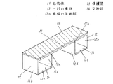
図1は本発明の一実施の形態における抵抗器の斜視図、図2は同抵抗器の正面図である。 FIG. 1 is a perspective view of a resistor according to an embodiment of the present invention, and FIG. 2 is a front view of the resistor.
本発明の一実施の形態における抵抗器は、図1、図2に示すように、金属板で構成した抵抗体11と、この抵抗体11の両端部において折り曲げられて抵抗体11と一体的に設けられた一対の電極12と、前記抵抗体11の少なくとも一部を覆うように設けられた保護膜13とを備え、そして前記一対の電極12の先端部12aを抵抗体11の下面に接続するとともに前記電極12に空隙部14を形成しているものである。
As shown in FIGS. 1 and 2, a resistor according to an embodiment of the present invention is integrally formed with a
上記構成において、前記抵抗体11は、ニクロム、銅ニッケル、マンガニン等の導電性の良好な板状の金属からなる金属板で構成され、その長さは1.0〜15mm、幅は0.5〜10mm、厚みは100〜1000μmとなっている。さらに、この抵抗体11の上面にはエポキシ樹脂、ポリイミド樹脂等の絶縁材からなる保護膜13が形成されている。なお、前記抵抗体11は一部に抵抗値調整用の切欠きを形成してもよいものである。
In the above configuration, the
また前記一対の電極12は、抵抗体11の両端部において抵抗体11と一体的に設けられ、かつ一部が下方に折り曲げられているもので、すなわち、この一対の電極12は、抵抗体11の両端部が下方に折り曲げられた第1側面部12bと、さらにその折り曲げられた部分の途中で抵抗体11の中央部に向かって折り曲げられた底面部12cと、さらにその途中で上方に折り曲げられた第2側面部12dとにより構成されている。また、前記第1側面部12b、底面部12c、第2側面部12dの長さは、抵抗体11の長さの1/10〜1/3となっている。
Further, the pair of
そして、前記第2側面部12dの先端部(電極12の先端部12a)は抵抗体11の下面と当接しているもので、この当接した部分において第2側面部12dと抵抗体11とが溶接等により接続されることにより、電極12にロ字状の空隙部14が形成される。
The distal end portion of the second
さらに、前記電極12の底面部12cの下面にはすずめっきが施されるもので、これにより抵抗器は実装基板に実装される。なお、このすずめっきと電極12の底面部12cの下面との間には必要に応じてニッケルめっき、銅めっき、金めっきを形成してもよいものである。
Further, the lower surface of the
次に、本発明の一実施の形態における抵抗器の製造方法について説明する。 Next, a method for manufacturing a resistor according to an embodiment of the present invention will be described.
図1、図2において、まず、板状の金属に、切断加工、打ち抜き加工、プレス加工等を施すことにより、所定形状の金属板を形成する。 1 and 2, first, a metal plate having a predetermined shape is formed by subjecting a plate-like metal to cutting, punching, pressing and the like.
次に、この金属板の両端部を下方に折り曲げて第1側面部12bを形成する。
Next, both end portions of the metal plate are bent downward to form the first
次に、その折り曲げられた部分の途中で抵抗体11の中央部に向かって折り曲げ、底面部12cを形成する。
Next, the
次に、その折り曲げられた部分の途中で上方に折り曲げて、第2側面部12dを形成し、電極12を設ける。このとき、第2側面部12dの先端部(電極12の先端部12a)を抵抗体11の下面と当接させる。
Next, the second
次に、電極12の先端部12aを抵抗体11の下面に溶接により接続する。
Next, the
次に、抵抗体11の上面に、保護膜13を熱圧着、超音波溶着等により形成する。このとき、抵抗体11の下面に位置する電極12の先端部12a間に保護膜13を形成してもよい。
Next, the
最後に、電極12の底面部12cの下面にすずめっきを形成する。
Finally, tin plating is formed on the lower surface of the
上記した本発明の一実施の形態においては、抵抗体11の両端部において前記抵抗体11と一体的に設けられた一対の電極12を、下方に折り曲げられた第1側面部12bと、さらにその折り曲げられた部分の途中で前記抵抗体11の中央部に向かって折り曲げられた底面部12cと、さらにその途中で上方に折り曲げられた第2側面部12dとにより構成するとともに、前記第2側面部12dの先端部12aを前記抵抗体11の下面に接続して前記一対の電極12に空隙部14を形成しているため、この空隙部14によって抵抗体11で発生した熱を放熱させることができ、これにより、抵抗体11が高温になるのを防止できるため、高電力印加時においても使用可能になるという効果が得られるものである。また、抵抗体11は高温とならないため、小型化も可能となるものである。
In one embodiment of the present invention described above, a first
そしてまた、前記電極12においては、金属板が空隙部14を介して抵抗体11と底面部12cとの上下に存在しているため、この金属板に上下方向の弾性を持たせることができ、これにより、上下方向の応力を緩和できるため、はんだが受ける力を低減でき、その結果、はんだの長寿命化も可能になるという効果も期待できるものである。
In addition, in the
さらに、電極12の先端部12a(第2側面部12dの先端部)と抵抗体11とを接続することにより、実装基板から流れる電流が、第1側面部12bと第2側面部12dの両方に並列で流れるため、抵抗値を下げることができる。
Further, by connecting the
なお、図3に示すように、空隙部14に金属体15を形成すれば、抵抗体11で発生した熱を金属体15に蓄熱させることができるため、抵抗体11の温度をより低下させることができ、これにより、さらなる高電力印加時においても使用可能となるものである。このとき、金属体15は底面部12cの上面に載置し、はんだ等で接続する。
As shown in FIG. 3, if the
本発明に係る抵抗器は、高電力印加時においても使用が可能となるものであり、各種電子機器の電流値検出等に使用される抵抗器において有用となるものである。 The resistor according to the present invention can be used even when high power is applied, and is useful in resistors used for detecting the current value of various electronic devices.
11 抵抗体
12 一対の電極
12a 電極の先端部
13 保護膜
14 空隙部
15 金属体
DESCRIPTION OF
Claims (2)
Priority Applications (1)
| Application Number | Priority Date | Filing Date | Title |
|---|---|---|---|
| JP2005329654A JP4887748B2 (en) | 2005-11-15 | 2005-11-15 | Resistor |
Applications Claiming Priority (1)
| Application Number | Priority Date | Filing Date | Title |
|---|---|---|---|
| JP2005329654A JP4887748B2 (en) | 2005-11-15 | 2005-11-15 | Resistor |
Publications (2)
| Publication Number | Publication Date |
|---|---|
| JP2007141906A JP2007141906A (en) | 2007-06-07 |
| JP4887748B2 true JP4887748B2 (en) | 2012-02-29 |
Family
ID=38204467
Family Applications (1)
| Application Number | Title | Priority Date | Filing Date |
|---|---|---|---|
| JP2005329654A Expired - Fee Related JP4887748B2 (en) | 2005-11-15 | 2005-11-15 | Resistor |
Country Status (1)
| Country | Link |
|---|---|
| JP (1) | JP4887748B2 (en) |
Families Citing this family (2)
| Publication number | Priority date | Publication date | Assignee | Title |
|---|---|---|---|---|
| US8325007B2 (en) * | 2009-12-28 | 2012-12-04 | Vishay Dale Electronics, Inc. | Surface mount resistor with terminals for high-power dissipation and method for making same |
| JP2021118279A (en) * | 2020-01-27 | 2021-08-10 | Koa株式会社 | Resistor |
Family Cites Families (5)
| Publication number | Priority date | Publication date | Assignee | Title |
|---|---|---|---|---|
| JPH0418219Y2 (en) * | 1986-07-31 | 1992-04-23 | ||
| JPH10229001A (en) * | 1997-02-14 | 1998-08-25 | Hokuriku Electric Ind Co Ltd | Surface-mounted type fixed resistor |
| JP2000068102A (en) * | 1998-08-25 | 2000-03-03 | Matsushita Electric Ind Co Ltd | Resistor |
| JP4012029B2 (en) * | 2002-09-30 | 2007-11-21 | コーア株式会社 | Metal plate resistor and manufacturing method thereof |
| JP4565556B2 (en) * | 2005-02-17 | 2010-10-20 | ローム株式会社 | Low resistance chip resistor and manufacturing method thereof |
-
2005
- 2005-11-15 JP JP2005329654A patent/JP4887748B2/en not_active Expired - Fee Related
Also Published As
| Publication number | Publication date |
|---|---|
| JP2007141906A (en) | 2007-06-07 |
Similar Documents
| Publication | Publication Date | Title |
|---|---|---|
| JP4670922B2 (en) | Low resistance resistor | |
| JP5599328B2 (en) | Connection mechanism between power semiconductor device and printed wiring board | |
| JP6074696B2 (en) | Resistor terminal connection structure | |
| JP2010514171A (en) | Resistor (especially SMD resistor) and manufacturing method thereof | |
| WO1996010490A1 (en) | Thermal printing head, and clip type terminal lead and cover used for the same | |
| EP4145471A1 (en) | Shunt resistor, shunt resistor manufacturing method, and current detecting device | |
| JP4887749B2 (en) | Resistor manufacturing method | |
| US20170162302A1 (en) | Current detection resistor | |
| JP4887748B2 (en) | Resistor | |
| JP4391918B2 (en) | Current detection resistor | |
| JP2006024825A (en) | Electrical component | |
| WO2006022257A1 (en) | Ceramic electronic component | |
| JP2002048821A (en) | Resistor for detecting current | |
| JP2009302117A (en) | Method for connecting tab pattern and lead wire | |
| JP4887973B2 (en) | Manufacturing method of surface mount type current fuse | |
| JP2008182078A (en) | Chip type metallic plate resistor | |
| JP5143353B2 (en) | Resistor manufacturing method | |
| JP2010218687A (en) | Fuse | |
| JP6500210B2 (en) | Metal plate resistor | |
| JP7329519B2 (en) | Semiconductor laser device | |
| JP2005197394A (en) | Metallic resistor | |
| US7974097B2 (en) | Printed circuit board and heat sink | |
| JP4384073B2 (en) | Manufacturing method of electronic parts | |
| JP2014060463A (en) | Chip resistor and method for manufacturing the same | |
| JP7446798B2 (en) | shunt resistance module |
Legal Events
| Date | Code | Title | Description |
|---|---|---|---|
| A621 | Written request for application examination |
Free format text: JAPANESE INTERMEDIATE CODE: A621 Effective date: 20080728 |
|
| RD01 | Notification of change of attorney |
Free format text: JAPANESE INTERMEDIATE CODE: A7421 Effective date: 20091126 |
|
| A131 | Notification of reasons for refusal |
Free format text: JAPANESE INTERMEDIATE CODE: A131 Effective date: 20110215 |
|
| A521 | Written amendment |
Free format text: JAPANESE INTERMEDIATE CODE: A523 Effective date: 20110413 |
|
| TRDD | Decision of grant or rejection written | ||
| A01 | Written decision to grant a patent or to grant a registration (utility model) |
Free format text: JAPANESE INTERMEDIATE CODE: A01 Effective date: 20111115 |
|
| A01 | Written decision to grant a patent or to grant a registration (utility model) |
Free format text: JAPANESE INTERMEDIATE CODE: A01 |
|
| A61 | First payment of annual fees (during grant procedure) |
Free format text: JAPANESE INTERMEDIATE CODE: A61 Effective date: 20111128 |
|
| FPAY | Renewal fee payment (event date is renewal date of database) |
Free format text: PAYMENT UNTIL: 20141222 Year of fee payment: 3 |
|
| LAPS | Cancellation because of no payment of annual fees |