JP4884592B2 - Method for manufacturing light emitting device and method for manufacturing display device - Google Patents
Method for manufacturing light emitting device and method for manufacturing display device Download PDFInfo
- Publication number
- JP4884592B2 JP4884592B2 JP2001072959A JP2001072959A JP4884592B2 JP 4884592 B2 JP4884592 B2 JP 4884592B2 JP 2001072959 A JP2001072959 A JP 2001072959A JP 2001072959 A JP2001072959 A JP 2001072959A JP 4884592 B2 JP4884592 B2 JP 4884592B2
- Authority
- JP
- Japan
- Prior art keywords
- substrate
- film
- manufacturing
- insulating film
- layer
- Prior art date
- Legal status (The legal status is an assumption and is not a legal conclusion. Google has not performed a legal analysis and makes no representation as to the accuracy of the status listed.)
- Expired - Fee Related
Links
- 238000000034 method Methods 0.000 title claims description 49
- 238000004519 manufacturing process Methods 0.000 title claims description 32
- 239000000758 substrate Substances 0.000 claims description 110
- 239000004033 plastic Substances 0.000 claims description 31
- 229920003023 plastic Polymers 0.000 claims description 31
- 239000012530 fluid Substances 0.000 claims description 25
- 239000004973 liquid crystal related substance Substances 0.000 claims description 25
- 239000002985 plastic film Substances 0.000 claims description 22
- 229920006255 plastic film Polymers 0.000 claims description 19
- 229910021426 porous silicon Inorganic materials 0.000 claims description 9
- 229910021417 amorphous silicon Inorganic materials 0.000 claims description 7
- 239000007788 liquid Substances 0.000 claims description 3
- 238000007743 anodising Methods 0.000 claims description 2
- 238000010030 laminating Methods 0.000 claims description 2
- 239000010410 layer Substances 0.000 description 70
- 238000005401 electroluminescence Methods 0.000 description 64
- 239000000463 material Substances 0.000 description 22
- 239000007789 gas Substances 0.000 description 17
- 239000011521 glass Substances 0.000 description 16
- 239000011347 resin Substances 0.000 description 15
- 229920005989 resin Polymers 0.000 description 15
- 238000000926 separation method Methods 0.000 description 13
- 238000002347 injection Methods 0.000 description 10
- 239000007924 injection Substances 0.000 description 10
- 230000008569 process Effects 0.000 description 10
- 239000000853 adhesive Substances 0.000 description 9
- 230000001070 adhesive effect Effects 0.000 description 9
- 239000003566 sealing material Substances 0.000 description 9
- 239000004065 semiconductor Substances 0.000 description 8
- VYPSYNLAJGMNEJ-UHFFFAOYSA-N silicon dioxide Inorganic materials O=[Si]=O VYPSYNLAJGMNEJ-UHFFFAOYSA-N 0.000 description 8
- XLYOFNOQVPJJNP-UHFFFAOYSA-N water Substances O XLYOFNOQVPJJNP-UHFFFAOYSA-N 0.000 description 8
- IJGRMHOSHXDMSA-UHFFFAOYSA-N Atomic nitrogen Chemical compound N#N IJGRMHOSHXDMSA-UHFFFAOYSA-N 0.000 description 7
- 229910021419 crystalline silicon Inorganic materials 0.000 description 7
- 229910052581 Si3N4 Inorganic materials 0.000 description 6
- 230000015572 biosynthetic process Effects 0.000 description 6
- HQVNEWCFYHHQES-UHFFFAOYSA-N silicon nitride Chemical compound N12[Si]34N5[Si]62N3[Si]51N64 HQVNEWCFYHHQES-UHFFFAOYSA-N 0.000 description 6
- 229910052814 silicon oxide Inorganic materials 0.000 description 6
- 229920000178 Acrylic resin Polymers 0.000 description 5
- XUIMIQQOPSSXEZ-UHFFFAOYSA-N Silicon Chemical compound [Si] XUIMIQQOPSSXEZ-UHFFFAOYSA-N 0.000 description 5
- 239000003990 capacitor Substances 0.000 description 5
- 239000003822 epoxy resin Substances 0.000 description 5
- 229920000647 polyepoxide Polymers 0.000 description 5
- -1 polyethylene Polymers 0.000 description 5
- 229920001721 polyimide Polymers 0.000 description 5
- 229910052710 silicon Inorganic materials 0.000 description 5
- 239000010703 silicon Substances 0.000 description 5
- 238000005507 spraying Methods 0.000 description 5
- 239000004925 Acrylic resin Substances 0.000 description 4
- CURLTUGMZLYLDI-UHFFFAOYSA-N Carbon dioxide Chemical compound O=C=O CURLTUGMZLYLDI-UHFFFAOYSA-N 0.000 description 4
- KRHYYFGTRYWZRS-UHFFFAOYSA-N Fluorane Chemical compound F KRHYYFGTRYWZRS-UHFFFAOYSA-N 0.000 description 4
- 238000000137 annealing Methods 0.000 description 4
- QVGXLLKOCUKJST-UHFFFAOYSA-N atomic oxygen Chemical compound [O] QVGXLLKOCUKJST-UHFFFAOYSA-N 0.000 description 4
- 238000010438 heat treatment Methods 0.000 description 4
- 239000001257 hydrogen Substances 0.000 description 4
- 229910052739 hydrogen Inorganic materials 0.000 description 4
- 239000011229 interlayer Substances 0.000 description 4
- 239000011159 matrix material Substances 0.000 description 4
- 229910052751 metal Inorganic materials 0.000 description 4
- 239000002184 metal Substances 0.000 description 4
- 239000001301 oxygen Substances 0.000 description 4
- 229910052760 oxygen Inorganic materials 0.000 description 4
- 239000004642 Polyimide Substances 0.000 description 3
- RTAQQCXQSZGOHL-UHFFFAOYSA-N Titanium Chemical compound [Ti] RTAQQCXQSZGOHL-UHFFFAOYSA-N 0.000 description 3
- NIXOWILDQLNWCW-UHFFFAOYSA-N acrylic acid group Chemical group C(C=C)(=O)O NIXOWILDQLNWCW-UHFFFAOYSA-N 0.000 description 3
- 229910001873 dinitrogen Inorganic materials 0.000 description 3
- 239000002019 doping agent Substances 0.000 description 3
- 230000005284 excitation Effects 0.000 description 3
- 229920002457 flexible plastic Polymers 0.000 description 3
- 238000005984 hydrogenation reaction Methods 0.000 description 3
- 239000012535 impurity Substances 0.000 description 3
- 238000000206 photolithography Methods 0.000 description 3
- 238000004544 sputter deposition Methods 0.000 description 3
- 238000003860 storage Methods 0.000 description 3
- 239000010936 titanium Substances 0.000 description 3
- 229910052719 titanium Inorganic materials 0.000 description 3
- 238000007740 vapor deposition Methods 0.000 description 3
- OKTJSMMVPCPJKN-UHFFFAOYSA-N Carbon Chemical compound [C] OKTJSMMVPCPJKN-UHFFFAOYSA-N 0.000 description 2
- LFQSCWFLJHTTHZ-UHFFFAOYSA-N Ethanol Chemical compound CCO LFQSCWFLJHTTHZ-UHFFFAOYSA-N 0.000 description 2
- UFHFLCQGNIYNRP-UHFFFAOYSA-N Hydrogen Chemical compound [H][H] UFHFLCQGNIYNRP-UHFFFAOYSA-N 0.000 description 2
- MHAJPDPJQMAIIY-UHFFFAOYSA-N Hydrogen peroxide Chemical compound OO MHAJPDPJQMAIIY-UHFFFAOYSA-N 0.000 description 2
- 239000004952 Polyamide Substances 0.000 description 2
- XLOMVQKBTHCTTD-UHFFFAOYSA-N Zinc monoxide Chemical compound [Zn]=O XLOMVQKBTHCTTD-UHFFFAOYSA-N 0.000 description 2
- 239000003929 acidic solution Substances 0.000 description 2
- 230000004913 activation Effects 0.000 description 2
- 239000012670 alkaline solution Substances 0.000 description 2
- 229910052782 aluminium Inorganic materials 0.000 description 2
- XAGFODPZIPBFFR-UHFFFAOYSA-N aluminium Chemical compound [Al] XAGFODPZIPBFFR-UHFFFAOYSA-N 0.000 description 2
- 239000012298 atmosphere Substances 0.000 description 2
- 230000008901 benefit Effects 0.000 description 2
- 230000000903 blocking effect Effects 0.000 description 2
- 238000007664 blowing Methods 0.000 description 2
- 229910052799 carbon Inorganic materials 0.000 description 2
- 239000001569 carbon dioxide Substances 0.000 description 2
- 229910002092 carbon dioxide Inorganic materials 0.000 description 2
- 239000000919 ceramic Substances 0.000 description 2
- 239000002131 composite material Substances 0.000 description 2
- 230000006835 compression Effects 0.000 description 2
- 238000007906 compression Methods 0.000 description 2
- 210000002858 crystal cell Anatomy 0.000 description 2
- 230000000694 effects Effects 0.000 description 2
- 238000005530 etching Methods 0.000 description 2
- 230000006870 function Effects 0.000 description 2
- 229910052736 halogen Inorganic materials 0.000 description 2
- RBTKNAXYKSUFRK-UHFFFAOYSA-N heliogen blue Chemical compound [Cu].[N-]1C2=C(C=CC=C3)C3=C1N=C([N-]1)C3=CC=CC=C3C1=NC([N-]1)=C(C=CC=C3)C3=C1N=C([N-]1)C3=CC=CC=C3C1=N2 RBTKNAXYKSUFRK-UHFFFAOYSA-N 0.000 description 2
- 150000002431 hydrogen Chemical class 0.000 description 2
- 238000002955 isolation Methods 0.000 description 2
- 229910052757 nitrogen Inorganic materials 0.000 description 2
- 239000012299 nitrogen atmosphere Substances 0.000 description 2
- 239000003960 organic solvent Substances 0.000 description 2
- 238000000059 patterning Methods 0.000 description 2
- 230000000737 periodic effect Effects 0.000 description 2
- 238000005268 plasma chemical vapour deposition Methods 0.000 description 2
- 229920003207 poly(ethylene-2,6-naphthalate) Polymers 0.000 description 2
- 229920006122 polyamide resin Polymers 0.000 description 2
- 239000004417 polycarbonate Substances 0.000 description 2
- 239000011112 polyethylene naphthalate Substances 0.000 description 2
- 229920000139 polyethylene terephthalate Polymers 0.000 description 2
- 239000005020 polyethylene terephthalate Substances 0.000 description 2
- 238000007639 printing Methods 0.000 description 2
- 239000010453 quartz Substances 0.000 description 2
- 239000000243 solution Substances 0.000 description 2
- JOHWNGGYGAVMGU-UHFFFAOYSA-N trifluorochlorine Chemical compound FCl(F)F JOHWNGGYGAVMGU-UHFFFAOYSA-N 0.000 description 2
- DTZWGKCFKSJGPK-VOTSOKGWSA-N (e)-2-(2-methyl-6-(2-(1,1,7,7-tetramethyl-1,2,3,5,6,7-hexahydropyrido[3,2,1-ij]quinolin-9-yl)vinyl)-4h-pyran-4-ylidene)malononitrile Chemical compound O1C(C)=CC(=C(C#N)C#N)C=C1\C=C\C1=CC(C(CCN2CCC3(C)C)(C)C)=C2C3=C1 DTZWGKCFKSJGPK-VOTSOKGWSA-N 0.000 description 1
- NBYLBWHHTUWMER-UHFFFAOYSA-N 2-Methylquinolin-8-ol Chemical class C1=CC=C(O)C2=NC(C)=CC=C21 NBYLBWHHTUWMER-UHFFFAOYSA-N 0.000 description 1
- YLYPIBBGWLKELC-RMKNXTFCSA-N 2-[2-[(e)-2-[4-(dimethylamino)phenyl]ethenyl]-6-methylpyran-4-ylidene]propanedinitrile Chemical compound C1=CC(N(C)C)=CC=C1\C=C\C1=CC(=C(C#N)C#N)C=C(C)O1 YLYPIBBGWLKELC-RMKNXTFCSA-N 0.000 description 1
- ZNJRONVKWRHYBF-VOTSOKGWSA-N 4-(dicyanomethylene)-2-methyl-6-julolidyl-9-enyl-4h-pyran Chemical compound O1C(C)=CC(=C(C#N)C#N)C=C1\C=C\C1=CC(CCCN2CCC3)=C2C3=C1 ZNJRONVKWRHYBF-VOTSOKGWSA-N 0.000 description 1
- ZOXJGFHDIHLPTG-UHFFFAOYSA-N Boron Chemical compound [B] ZOXJGFHDIHLPTG-UHFFFAOYSA-N 0.000 description 1
- ISWSIDIOOBJBQZ-UHFFFAOYSA-N Phenol Chemical class OC1=CC=CC=C1 ISWSIDIOOBJBQZ-UHFFFAOYSA-N 0.000 description 1
- 239000004698 Polyethylene Substances 0.000 description 1
- NRCMAYZCPIVABH-UHFFFAOYSA-N Quinacridone Chemical compound N1C2=CC=CC=C2C(=O)C2=C1C=C1C(=O)C3=CC=CC=C3NC1=C2 NRCMAYZCPIVABH-UHFFFAOYSA-N 0.000 description 1
- 238000001069 Raman spectroscopy Methods 0.000 description 1
- UCKMPCXJQFINFW-UHFFFAOYSA-N Sulphide Chemical compound [S-2] UCKMPCXJQFINFW-UHFFFAOYSA-N 0.000 description 1
- 229910001080 W alloy Inorganic materials 0.000 description 1
- 239000003570 air Substances 0.000 description 1
- 238000002048 anodisation reaction Methods 0.000 description 1
- 125000004429 atom Chemical group 0.000 description 1
- UFVXQDWNSAGPHN-UHFFFAOYSA-K bis[(2-methylquinolin-8-yl)oxy]-(4-phenylphenoxy)alumane Chemical compound [Al+3].C1=CC=C([O-])C2=NC(C)=CC=C21.C1=CC=C([O-])C2=NC(C)=CC=C21.C1=CC([O-])=CC=C1C1=CC=CC=C1 UFVXQDWNSAGPHN-UHFFFAOYSA-K 0.000 description 1
- 229910052796 boron Inorganic materials 0.000 description 1
- 239000000969 carrier Substances 0.000 description 1
- 230000008859 change Effects 0.000 description 1
- 239000003795 chemical substances by application Substances 0.000 description 1
- 238000000576 coating method Methods 0.000 description 1
- XCJYREBRNVKWGJ-UHFFFAOYSA-N copper(II) phthalocyanine Chemical compound [Cu+2].C12=CC=CC=C2C(N=C2[N-]C(C3=CC=CC=C32)=N2)=NC1=NC([C]1C=CC=CC1=1)=NC=1N=C1[C]3C=CC=CC3=C2[N-]1 XCJYREBRNVKWGJ-UHFFFAOYSA-N 0.000 description 1
- VBVAVBCYMYWNOU-UHFFFAOYSA-N coumarin 6 Chemical compound C1=CC=C2SC(C3=CC4=CC=C(C=C4OC3=O)N(CC)CC)=NC2=C1 VBVAVBCYMYWNOU-UHFFFAOYSA-N 0.000 description 1
- 230000007423 decrease Effects 0.000 description 1
- 230000006866 deterioration Effects 0.000 description 1
- AJNVQOSZGJRYEI-UHFFFAOYSA-N digallium;oxygen(2-) Chemical compound [O-2].[O-2].[O-2].[Ga+3].[Ga+3] AJNVQOSZGJRYEI-UHFFFAOYSA-N 0.000 description 1
- 238000009826 distribution Methods 0.000 description 1
- 238000001704 evaporation Methods 0.000 description 1
- 229910001195 gallium oxide Inorganic materials 0.000 description 1
- 230000005525 hole transport Effects 0.000 description 1
- 230000006872 improvement Effects 0.000 description 1
- 238000005224 laser annealing Methods 0.000 description 1
- 239000003446 ligand Substances 0.000 description 1
- 230000007246 mechanism Effects 0.000 description 1
- 239000011259 mixed solution Substances 0.000 description 1
- 230000003287 optical effect Effects 0.000 description 1
- 239000011368 organic material Substances 0.000 description 1
- 230000003647 oxidation Effects 0.000 description 1
- 238000007254 oxidation reaction Methods 0.000 description 1
- 238000002161 passivation Methods 0.000 description 1
- 125000002080 perylenyl group Chemical group C1(=CC=C2C=CC=C3C4=CC=CC5=CC=CC(C1=C23)=C45)* 0.000 description 1
- CSHWQDPOILHKBI-UHFFFAOYSA-N peryrene Natural products C1=CC(C2=CC=CC=3C2=C2C=CC=3)=C3C2=CC=CC3=C1 CSHWQDPOILHKBI-UHFFFAOYSA-N 0.000 description 1
- 229920000515 polycarbonate Polymers 0.000 description 1
- 229910021420 polycrystalline silicon Inorganic materials 0.000 description 1
- 229920000573 polyethylene Polymers 0.000 description 1
- 239000009719 polyimide resin Substances 0.000 description 1
- 229920000642 polymer Polymers 0.000 description 1
- 230000001681 protective effect Effects 0.000 description 1
- 238000007789 sealing Methods 0.000 description 1
- HBMJWWWQQXIZIP-UHFFFAOYSA-N silicon carbide Chemical compound [Si+]#[C-] HBMJWWWQQXIZIP-UHFFFAOYSA-N 0.000 description 1
- 229910010271 silicon carbide Inorganic materials 0.000 description 1
- 239000007787 solid Substances 0.000 description 1
- 238000001179 sorption measurement Methods 0.000 description 1
- 230000003595 spectral effect Effects 0.000 description 1
- 238000004528 spin coating Methods 0.000 description 1
- 238000002230 thermal chemical vapour deposition Methods 0.000 description 1
- 229920001187 thermosetting polymer Polymers 0.000 description 1
- 238000002834 transmittance Methods 0.000 description 1
- WFKWXMTUELFFGS-UHFFFAOYSA-N tungsten Chemical compound [W] WFKWXMTUELFFGS-UHFFFAOYSA-N 0.000 description 1
- 229910052721 tungsten Inorganic materials 0.000 description 1
- 239000010937 tungsten Substances 0.000 description 1
- 239000011787 zinc oxide Substances 0.000 description 1
Images


Classifications
-
- H—ELECTRICITY
- H10—SEMICONDUCTOR DEVICES; ELECTRIC SOLID-STATE DEVICES NOT OTHERWISE PROVIDED FOR
- H10K—ORGANIC ELECTRIC SOLID-STATE DEVICES
- H10K59/00—Integrated devices, or assemblies of multiple devices, comprising at least one organic light-emitting element covered by group H10K50/00
- H10K59/10—OLED displays
- H10K59/12—Active-matrix OLED [AMOLED] displays
- H10K59/1201—Manufacture or treatment
-
- H—ELECTRICITY
- H01—ELECTRIC ELEMENTS
- H01L—SEMICONDUCTOR DEVICES NOT COVERED BY CLASS H10
- H01L2221/00—Processes or apparatus adapted for the manufacture or treatment of semiconductor or solid state devices or of parts thereof covered by H01L21/00
- H01L2221/67—Apparatus for handling semiconductor or electric solid state devices during manufacture or treatment thereof; Apparatus for handling wafers during manufacture or treatment of semiconductor or electric solid state devices or components; Apparatus not specifically provided for elsewhere
- H01L2221/683—Apparatus for handling semiconductor or electric solid state devices during manufacture or treatment thereof; Apparatus for handling wafers during manufacture or treatment of semiconductor or electric solid state devices or components; Apparatus not specifically provided for elsewhere for supporting or gripping
- H01L2221/68304—Apparatus for handling semiconductor or electric solid state devices during manufacture or treatment thereof; Apparatus for handling wafers during manufacture or treatment of semiconductor or electric solid state devices or components; Apparatus not specifically provided for elsewhere for supporting or gripping using temporarily an auxiliary support
- H01L2221/68363—Apparatus for handling semiconductor or electric solid state devices during manufacture or treatment thereof; Apparatus for handling wafers during manufacture or treatment of semiconductor or electric solid state devices or components; Apparatus not specifically provided for elsewhere for supporting or gripping using temporarily an auxiliary support used in a transfer process involving transfer directly from an origin substrate to a target substrate without use of an intermediate handle substrate
-
- H—ELECTRICITY
- H10—SEMICONDUCTOR DEVICES; ELECTRIC SOLID-STATE DEVICES NOT OTHERWISE PROVIDED FOR
- H10K—ORGANIC ELECTRIC SOLID-STATE DEVICES
- H10K59/00—Integrated devices, or assemblies of multiple devices, comprising at least one organic light-emitting element covered by group H10K50/00
- H10K59/10—OLED displays
- H10K59/12—Active-matrix OLED [AMOLED] displays
-
- H—ELECTRICITY
- H10—SEMICONDUCTOR DEVICES; ELECTRIC SOLID-STATE DEVICES NOT OTHERWISE PROVIDED FOR
- H10K—ORGANIC ELECTRIC SOLID-STATE DEVICES
- H10K71/00—Manufacture or treatment specially adapted for the organic devices covered by this subclass
- H10K71/80—Manufacture or treatment specially adapted for the organic devices covered by this subclass using temporary substrates
Landscapes
- Liquid Crystal (AREA)
- Engineering & Computer Science (AREA)
- Devices For Indicating Variable Information By Combining Individual Elements (AREA)
- Manufacturing & Machinery (AREA)
- Microelectronics & Electronic Packaging (AREA)
- Electroluminescent Light Sources (AREA)
- Thin Film Transistor (AREA)
Description
【0001】
【発明の属する技術分野】
本発明は、電極間に発光性材料を挟んだ素子(以下、発光素子という)を有する装置(以下、発光装置という)もしくは電極間に液晶を挟んだ素子(以下、液晶素子という)を有する装置(以下、液晶表示装置という)の作製方法に関する。なお、有機ELディスプレイや有機発光ダイオード(OLED:Organic Light Emitting Diode)は本発明の発光装置に含まれる。
【0002】
また、本明細書中では、発光装置及び液晶表示装置を総称して表示装置(電気光学装置)と呼ぶ。
【0003】
また、本発明に用いることのできる発光性材料は、一重項励起もしくは三重項励起または両者の励起を経由して発光(燐光および/または蛍光)するすべての発光性材料を含む。
【0004】
【従来の技術】
近年、EL(Electro Luminescence)が得られる発光性材料(以下、EL材料という)を利用した発光素子(以下、EL素子という)を用いた発光装置(以下、EL発光装置という)の開発が進んでいる。EL発光装置は、陽極と陰極との間にEL材料を挟んだ構造のEL素子を有した構造からなる。この陽極と陰極との間に電圧を加えてEL材料中に電流を流することによりキャリアを再結合させて発光させる。即ち、EL発光装置は発光素子自体に発光能力があるため、液晶表示装置に用いるようなバックライトが不要である。さらに視野角が広く、軽量であり、且つ、低消費電力という利点をもつ。
【0005】
このようなEL発光装置を利用したアプリケーションは様々なものが期待されているが、特にEL発光装置の厚みが薄いこと、従って軽量化が可能であることにより携帯機器への利用が注目されている。そのため、フレキシブルなプラスチックフィルムの上に発光素子を形成することが試みられている。
【0006】
しかしながら、プラスチックフィルムの耐熱性が低いためプロセスの最高温度を低くせざるを得ず、結果的にガラス基板上に形成する時ほど良好な電気特性のTFTを形成できないのが現状である。そのため、プラスチックフィルムを用いた高性能な表示装置は実現されていない。
【0007】
【発明が解決しようとする課題】
本願発明はプラスチック支持体(可撓性のプラスチックフィルムもしくはプラスチック基板を含む。)を用いて高性能な表示装置を作製するための技術を提供することを課題とする。
【0008】
【課題を解決するための手段】
本発明は、プラスチックに比べて耐熱性のある基板(ガラス基板、石英基板、シリコン基板、金属基板もしくはセラミックス基板)の上に必要な素子を形成し、後にそれらの素子を室温の処理によりプラスチック基板(プラスチックフィルムも含む)に移すことを特徴とする。
【0009】
なお、前記必要な素子とは、アクティブマトリクス型の表示装置ならば画素のスイッチング素子として用いる半導体素子(典型的にはTFT)もしくはMIM素子並びに発光素子もしくは液晶素子を指す。また、パッシブ型の表示装置ならば発光素子もしくは液晶素子を指す。なお、本明細書中では半導体素子やMIM素子を能動素子と呼び、発光素子や液晶素子を受動素子と呼ぶ。
【0010】
また、プラスチック基板としてはポリイミド、エポキシ樹脂、アクリル樹脂、PES(ポリエチレンサルファイル)、PC(ポリカーボネート)、PET(ポリエチレンテレフタレート)もしくはPEN(ポリエチレンナフタレート)からなる基板もしくはフィルムを用いることができる。
【0011】
本発明では上記素子を剥離層の上に形成しておき、後にその剥離層に向けて流体を吹きつけることにより素子が形成された基板を分離し、新たにプラスチック基板を貼り付けることを特徴としている。剥離層としては、多孔質シリコン層又は水素、酸素、窒素もしくは希ガスを添加したシリコン層を用いる。
【0012】
また、流体の吹きつけ方法としては、高圧の水流をノズルから噴射して吹きつける方法(ウォータージェット法と呼ばれる)や高圧のガス流を噴射して吹きつける方法を用いることができる。このとき、水の代わりに有機溶媒、酸性溶液もしくはアルカリ性溶液を用いても良い。また、ガスとしては空気、窒素ガス、炭酸ガスもしくは希ガスを用いても良いし、これらのガスをプラズマ化したものであっても良い。
【0013】
これらの流体を剥離層に吹きつけると、剥離層が脆性により崩壊するか化学的に除去される。これにより素子が形成された基板と、その素子の下地として設けられていた絶縁膜とが分離されることになる。剥離層の崩壊により分離させた場合、残存した剥離層は改めてエッチングにより除去すれば良い。
【0014】
こうして素子の下地となる絶縁膜を露出させ、新しくプラスチックからなる基板もしくはフィルムを貼り付ける。貼り付ける際には、光硬化性樹脂、熱硬化性樹脂もしくはエポキシ系樹脂を接着剤として用いることができる。
【0015】
以上のように、本発明ではまずプラスチックよりも耐熱性の高い基板(素子形成基板)上に半導体素子やMIM素子といった能動素子もしくは発光素子や液晶素子といった受動素子を形成し、最後に前記素子形成基板をプラスチックからなる基板に貼り替える。その貼り替えの際に高圧水もしくは高圧ガスを用いて基板の分離を行う点に特徴がある。
【0016】
また、高圧の流体を複合部材の側面に吹きつけて該複合部材を分離する手段およびそのための装置として、特開平11−45840号公報、特開平11−5064号公報、特開平11−195563号公報、特開平11−195568号公報、特開平11−195569号公報、特開平11−195570号公報を本発明に引用することは可能である。
【0017】
【発明の実施の形態】
本発明の実施の形態について説明する。図1は本発明の概略図であり、101はガラス基板、102は剥離層、103は下地となる絶縁膜、104は絶縁膜103上に形成された素子、105は樹脂からなる絶縁膜、106はプラスチックフィルムである。
【0018】
ガラス基板101は石英基板、金属基板もしくはセラミックス基板であっても良い。また、剥離層102はここでは多孔質シリコン膜を用いるが、水素、酸素、窒素もしくは希ガスを添加したシリコン層であっても良い。多孔質シリコン膜を用いる場合、非晶質シリコン膜もしくは多結晶シリコン膜を陽極化成処理により多孔質化して用いれば良い。なお、剥離層102の膜厚は0.1〜900μm(好ましくは0.5〜10μm)で良い。
【0019】
また、絶縁膜103は珪素を含む絶縁膜を用いれば良い。珪素を含む絶縁膜としては、酸化シリコン膜、窒化シリコン膜、窒化酸化シリコン膜もしくは炭化シリコン膜を用いることができる。さらにその上に形成される素子104は半導体素子やMIM素子などの能動素子と発光素子や液晶素子などの受動素子を組み合わせたものであっても良いし、発光素子や液晶素子であっても良い。
【0020】
樹脂からなる絶縁膜105は素子104を外気から保護するための封止材としての役割とプラスチックフィルム106を貼り付ける接着材としての役割の両方を持つ。代表的には紫外線硬化樹脂を用いれば良い。また、プラスチックフィルム106の代わりにガラス基板を用いても良い。
【0021】
以上のような構造を含む表示装置を、中心を軸にして矢印のように回転させ、さらにノズル107から流体108を噴射させる。ノズル107からは1×10⁷〜1×10⁹Pa(好ましくは3×10⁷〜5×10⁸Pa)の圧力が加わった流体が噴射されて剥離層102の側面に吹きつけられる。流体108は試料が回転しているため剥離層102の露出面に沿って吹きつけられていく。その衝撃により剥離層102は崩壊もしくは除去され、ガラス基板101と絶縁膜103とが分離される。
【0022】
なお、流体108は水、有機溶媒、酸性溶液もしくはアルカリ性溶液といった液体を用いても良い、空気、窒素ガス、炭酸ガスもしくは希ガスといった気体を用いても良い。さらにこれらのガスをプラズマ化したものでも良い。
【0023】
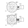
図1の状態を上面から見ると図2に示すようになる。なお、図2(A)は素子を形成する母体基板として丸い基板を用いた試料201であり、試料201には202で示される単位で表示装置が形成されている。これは一枚の基板から複数の表示装置を作製する場合の例である。また、同様に図2(B)は四角い基板を用いた試料203であり、試料203には204で示される単位で表示装置が形成されている。
【0024】
このとき、ノズル107の噴出口は長楕円形状もしくは長方形状となっており、流体108の断面形状はノズルの形状とほぼ一致している。円形状や四角形状としても構わないが、長楕円形状もしくは長方形状とした方が処理効率は高い。
【0025】
また、ここではノズルを一つしか図示していないが、二つ以上のノズルを設けても良い。その際、基板の一辺に対して複数並べて設けても良いし、基板の各辺ごとに一つ乃至複数のノズルを設けても良い。
【0026】
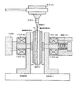
次に、本発明において流体108を噴射する装置(以下、分離装置という)の概略の構造を図3に示す。図3に示す分離装置では図1に示すような構造を含む試料301が基板保持体302、303により保持されている。基板保持体302、303は各々真空吸着により試料301を保持している。
【0027】
また、基板保持体302、303は互いに同一回転軸上に配置され、回転しうるように設けられている。また、基板保持体302はベアリング304、305に嵌合されて支持台306に支持される。さらに、基板保持体302はモータ307に連結されており、回転スピードの調節が行えるようになっている。
【0028】
一方、基板保持体303はベアリング308、309に嵌合されて支持台310に支持される。また、基板保持体303は圧縮バネ311により右方向に引っ張られた状態となっており、その力と基板保持体303の吸着力とを釣り合わせることにより試料301を保持している。
【0029】
この状態でポンプ315からノズル316へと高圧の流体が送り込まれ、この流体317が試料301の内部に設けられた剥離層102に向けて噴射される構成となっている。流体317が噴射されている間、基板保持体302、303は試料301を挟んだまま回転する。
【0030】
こうして剥離層102に流体317が吹きつけられると剥離層102の崩壊が始まり、ガラス基板101とプラスチック基板106との間が徐々に押し広げられていく。さらに、圧縮バネ311により基板保持体303には右方向への力が加わっているため、剥離層102の崩壊が進むと最終的にはガラス基板101とプラスチック基板106とが分離される。
【0031】
なお、本発明の実施の形態では、試料301を回転させる例を示しているが、ノズル316が試料301の側面に沿って回転し、高圧の流体を噴射する構成とすることも可能である。
【0032】
【実施例】
〔実施例1〕
本実施例ではEL発光装置の画素部の作製工程について図4、5を用いて説明する。また、本実施の形態によって作製される画素の上面図を図6に示す。なお、図6に用いた符号は図4、5で用いた符号に対応している。
【0033】
まずガラス基板401上に多孔質シリコン膜からなる剥離層402を1μmの厚さに形成する。多孔質シリコン膜は非晶質シリコン膜を成膜して、該非晶質シリコン膜を、フッ酸:水:エタノールを1:1:1の割合で混合した溶液中で陽極化成処理を行って形成すれば良い。
【0034】
次に、剥離層402の上に下地膜403として窒化酸化シリコン膜を200nmの厚さに形成する。下地膜403の形成は減圧熱CVD法、プラズマCVD法、スパッタ法もしくは蒸着法を用いれば良い。
【0035】
次に、下地膜103の上に後に結晶質シリコン膜404を50nmの厚さに形成する。結晶質シリコン膜404の形成方法としては公知の手段を用いることが可能である。固体レーザーもしくはエキシマレーザーを用いて非晶質シリコン膜をレーザー結晶化させても良いし、非晶質シリコン膜を加熱処理(ファーネスアニール)により結晶化させても良い。
【0036】
次に、図4(B)に示すように、結晶質シリコン膜404をパターニングしてパターン化した結晶質シリコン膜405、406を形成する。そしてパターン化した結晶質シリコン膜を覆って酸化シリコン膜からなるゲート絶縁膜407を80nmの厚さに形成する。さらに、ゲート絶縁膜407の上にゲート電極408、409を形成する。本実施例ではゲート電極408、409の材料として、350nm厚のタングステン膜もしくはタングステン合金膜を用いる。勿論、ゲート電極の材料としては他の公知の材料を用いることができる。
【0037】
そして、ゲート電極408、409をマスクとして周期表の13族に属する元素(代表的にはボロン)を添加する。添加方法は公知の手段を用いれば良い。こうしてp型の導電型を示す不純物領域(以下、p型不純物領域という)410〜414が形成される。また、ゲート電極の直下にはチャネル形成領域415〜417が画定する。なお、p型不純物領域410〜414はTFTのソース領域もしくはドレイン領域となる。
【0038】
次に、図4(C)に示すように、窒化シリコン膜418を50nmの厚さに形成し、その後、加熱処理を行って添加された周期表の13族に属する元素の活性化を行う。この活性化はファーネスアニール、レーザーアニールもしくはランプアニールにより行うか、又はそれらを組み合わせて行えば良い。本実施例では500℃4時間の加熱処理を窒素雰囲気で行う。
【0039】
活性化が終了したら、水素化処理を行うと効果的である。水素化処理は公知の水素アニール技術もしくはプラズマ水素化技術を用いれば良い。
【0040】
次に、図4(D)に示すように、酸化シリコン膜からなる第1層間絶縁膜419を800nmの厚さに形成し、コンタクトホールを形成して配線420〜423を形成する。第1層間絶縁膜419としては他の無機絶縁膜を用いても良いし、樹脂(有機絶縁膜)を用いても良い。本実施の形態では配線420〜423としてチタン/アルミニウム/チタンの三層構造からなる金属配線を用いる。勿論、導電膜であれば如何なる材料を用いても良い。配線420〜423はTFTのソース配線もしくはドレイン配線となる。
【0041】
この状態でスイッチング用TFT501及び電流制御用TFT(駆動用TFT)502が完成する。本実施の形態ではどちらのTFTもpチャネル型TFTで形成される。但し、スイッチング用TFT501はゲート電極がパターン化された結晶質シリコン膜を二カ所で横切るように形成されており、二つのチャネル形成領域が直列に接続された構造となっている。このような構造とすることでオフ電流値(TFTがオフされた時に流れる電流)を抑制することができる。
【0042】
また、同時に図6(B)に示すように保持容量601が形成される。保持容量601は活性層と同時に形成された半導体層602、ゲート絶縁膜407及びゲート電極409で形成される下側保持容量と、ゲート電極409、第1層間絶縁膜419及び配線423で形成される上側保持容量とで形成される。また、半導体層602は配線423と電気的に接続されている。
【0043】
次に、図4(E)に示すように、酸化物導電膜(本実施例では酸化亜鉛に酸化ガリウムを添加した導電膜)を100nmの厚さに形成し、パターニングにより画素電極424を形成する。このとき、配線422と画素電極424とはオーミック接触をする。従って、画素電極424と電流制御用TFT502とは電気的に接続される。また、画素電極424はEL素子の陽極として機能する。
【0044】
画素電極424を形成したら、酸化シリコン膜からなる第2層間絶縁膜425を300nmの厚さに形成する。そして、開口部426を形成し、70nm厚の有機EL層427及び300nm厚の陰極428を蒸着法により形成する。本実施例では有機EL層427として20nm厚の正孔注入層及び50nm厚の発光層を積層した構造を用いる。勿論、発光層に正孔注入層、正孔輸送層、電子輸送層、電子注入層、正孔阻止層もしくは電子阻止層を組み合わせた公知の他の構造を用いても良い。
【0045】
本実施例では、正孔注入層としてCuPc(銅フタロシアニン)を用いる。この場合、まず全ての画素電極を覆うように銅フタロシアニンを形成し、その後、赤色、緑色及び青色に対応する画素ごとに各々赤色の発光層、緑色の発光層及び青色の発光層を形成する。形成する領域の区別は蒸着時にシャドーマスクを用いて行えば良い。このようにすることでカラー表示が可能となる。
【0046】
なお、本実施例では緑色の発光層の母体材料としてAlq3(トリス−8−キノリノラトアルミニウム錯体)を用い、キナクリドンもしくはクマリン6をドーパントとして添加する。また、赤色の発光層の母体材料としてAlq3を用い、DCJT、DCM1もしくはDCM2をドーパントとして添加する。また、青色の発光層の母体材料としてBAlq3(2−メチル−8−キノリノールとフェノール誘導体の混合配位子を持つ5配位の錯体)を用い、ペリレンをドーパントとして添加する。
【0047】
勿論、本願発明では上記有機材料に限定する必要はなく、公知の低分子系有機EL材料、高分子系有機EL材料もしくは無機EL材料を用いることが可能である。高分子系有機EL材料を用いる場合は塗布法を用いることもできる。
【0048】
以上のようにして、画素電極(陽極)424、有機EL層427及び陰極428からなるEL素子(図6(B)において602で示される)が形成される。本実施例ではこのEL素子が発光素子として機能する。
【0049】
次に、図5(A)に示すように、封止材429によりプラスチック基板430を貼り合わせる。本実施例ではプラスチック基板430として可撓性のプラスチックフィルムを用いる。また、封止材429としては、樹脂からなる絶縁膜を用いることができ、本実施例ではポリイミドを用いる。そのほかにもアクリル樹脂、ポリアミドもしくはエポキシ樹脂を用いても良い。
【0050】
図5(A)のプロセスを行うことによりEL素子を完全に大気から遮断することができる。これにより酸化による有機EL材料の劣化をほぼ完全に抑制することができ、EL素子の信頼性を大幅に向上させることができる。
【0051】
次に、図5(B)に示すように、EL素子の形成された基板からガラス基板101を分離する。この分離工程は、図1〜3に説明した本発明の分離装置を用いて行えば良い。本実施例では、長楕円形状のノズルから3×10⁷Paの圧力で水流を噴射し、剥離層402を崩壊させる。その後、下地膜403に残存した剥離層402をフッ酸と過酸化水素水との混合溶液で除去する。この溶液は多孔質シリコン膜からなる剥離層402を選択的に除去することが可能である。
【0052】
こうしてプラスチック基板430にTFT及びEL素子を移したら、図5(C)に示すように、接着剤431を形成し、プラスチックフィルム432を貼り合わせる。接着剤431としては樹脂からなる絶縁膜(代表的にはポリイミド、アクリル、ポリアミドもしくはエポキシ樹脂)を用いても良いし、無機絶縁膜(代表的には酸化シリコン膜)を用いても良い。
【0053】
こうしてガラス基板401からプラスチックフィルム432へとTFT及びEL素子が移される。その結果、二枚のプラスチックフィルム430、432によって挟まれたフレキシブルなEL発光装置を得ることができる。
【0054】
なお、本実施例において、このように発光素子の上に設けた支持用のプラスチックフィルム430と貼り合わせ用のプラスチックフィルム432を同一材料した理由は熱膨張係数を揃えるためである。熱膨張係数が等しいと、温度変化による基板の応力歪みのバランスがとれ、発光素子に与える影響を抑制することができるので好ましい。
【0055】
また、本実施例により作製されたEL発光装置は、フォトリソグラフィに必要なマスク枚数がトータルで6枚と非常に少なく、高い歩留まりと低い製造コストを達成することができる。また、こうして形成されたEL発光装置は、プラスチック基板の耐熱性に制限されることなく形成されたTFTを能動素子として用いることができるので高性能なものとすることができる。
【0056】
なお、本実施例では、TFTの例としてトップゲート構造のTFT(具体的にはプレーナ型TFT)を示したが、ボトムゲート構造のTFT(典型的には逆スタガ型TFT)としても良い。
【0057】
〔実施例2〕
実施例1において、ゲート電極を形成するところまでの作製工程として本出願人による特開平9−312260号公報、特開平10−247735号公報、特開平10−270363号公報もしくは特開平11−191628号公報のいずれかに記載の発明を用いることは有効である。
【0058】
上記公報に記載された技術はいずれも非常に高い結晶性を有する結晶質シリコン膜を形成するための技術であり、これらの技術を用いることで高性能なTFTを形成することが可能である。これらの技術はいずれも550℃以上の加熱処理を含むが、本発明の技術を用いることで、素子形成基板として耐熱性の低いプラスチック基板を用いることが可能となる。
【0059】
なお、本実施例の構成は、実施例1の構成と自由に組み合わせて実施することが可能である。
【0060】
〔実施例3〕
本実施例では本発明を液晶表示装置に用いた場合の例について説明する。説明には図7を用いる。
【0061】
図7(A)において、701はガラス基板、702は非晶質シリコン層に1×10¹⁶〜1×10¹⁷atoms/cm3の濃度で水素を含む剥離層、703は窒化酸化シリコン膜からなる下地膜、704は画素TFTである。画素TFT704は実施例1に説明した工程に従って作製されたpチャネル型TFTであり、本実施例では液晶に加えられる電圧を制御するためのスイッチング素子として用いる。また、705は画素TFT704に電気的に接続された酸化物導電膜からなる画素電極である。
【0062】
以上に説明した構造までは実施例1で説明した作製工程に従えば良い。勿論、TFTの構造はボトムゲート型(代表的には逆スタガ型)とすることも可能であり、TFTの作製工程を実施例1の工程に限定する必要はない。
【0063】
画素TFT704及び画素電極705を形成したら、樹脂からなる配向膜706を形成する。配向膜706は印刷法により形成すれば良い。また、膜厚は60nmとする。
【0064】
次に、プラスチックフィルムからなる対向基板707を用意し、その上にスパッタ法によりチタンからなる遮光膜708を120nmの厚さに、酸化物導電膜からなる対向電極709を110nmの厚さに形成する。その上には配向膜710を60nmの厚さに形成する。
【0065】
次に、TFTの形成された基板側の配向膜706の上にシール材(図示せず)をディスペンサー等の手段により形成し、配向膜706と対向基板側の配向膜710とを向かい合わせて貼り合わせ、加圧プレスして接着する。さらに、シール材に囲まれた領域に真空注入法を用いて液晶711を注入し、シール材の注入口を樹脂で塞いで液晶素子(液晶セルと言っても良い)を完成させる。これらの工程は公知の液晶セルの作製工程を実施すれば良い。このとき、シール材としてはポリイミド、アクリルもしくはエポキシ樹脂を用いる。このシール剤は図5(A)の封止材429と同様に接着剤としての役割を果たす。
【0066】
次に、図7(B)に示すように、液晶素子の形成された基板からガラス基板701を分離する。この分離工程は、図1〜3に説明した本発明の分離装置を用いて行えば良い。本実施例では、長楕円形状のノズルから5×10⁷Paの圧力で水流を噴射し、剥離層702を崩壊させる。
【0067】
その後、下地膜703に残存した剥離層702を、フッ化ハロゲンを含むガス中で除去する。フッ化ハロゲンを含むガスとしては、窒素ガスと三フッ化塩素ガスを混合させたガスを用いる。この処理は室温で行うことができる。
【0068】
こうして最終的には剥離層702が完全に除去され、窒化酸化シリコン膜からなる下地膜703が露呈する。そして最後に、アクリル膜からなる接着剤712を用いてプラスチックフィルム713を接着する。
【0069】
以上のように、本発明を液晶表示装置に用いる場合は液晶の注入工程までを完了させて一旦液晶表示装置を完成させ、その後に対向基板で素子を固定しつつ剥離層の除去工程を行うことができる。そのため、特に煩雑な工程を増やすことなく、高性能なTFTをプラスチック基板の上に形成できる。なお、本実施例の構成に実施例2の構成を組み合わせて実施することは可能である。
【0070】
〔実施例4〕
本実施例では本発明を単純マトリクス型EL発光装置に用いた場合の例について説明する。説明には図8を用いる。
【0071】
図8(A)において、801はガラス基板、802は多孔質シリコン膜からなる剥離層、803は酸化シリコン膜からなる下地膜、804は第1のストライプ電極であり、本実施例では酸化物導電膜からなる陽極である。この陽極804は紙面と平行な方向にストライプ状に複数本形成されている。
【0072】
陽極804上には素子分離用絶縁膜805及び樹脂膜からなるバンク806がストライプ状に複数本形成される。なお、このバンプ806は二層の樹脂膜を積層して形成されており、上層側よりも下層側の方が内側に狭い形状となっている。このような構造は二層の樹脂膜のエッチングレートの差を利用して形成することができる。
【0073】
これらは前述の陽極804と直交するように形成される。こうして素子分離用絶縁膜805及び樹脂膜からなるバンク806を形成したら、有機EL層807、第2のストライプ電極(本実施例では金属膜からなる陰極)808を蒸着法により形成する。陰極808はバンク806によってストライプ状に分離されて形成されるため、陽極804と直交するように形成される。
【0074】
この時、陽極804、有機EL層807及び陰極808で形成されるコンデンサがEL素子となる。勿論、陽極804、有機EL層807及び陰極808の形成方法もしくは形成材料は公知のものを用いることができる。
【0075】
EL素子が形成されたら、封止材(本実施例ではアクリル樹脂)809を用いてプラスチックフィルム810を接着する。こうしてEL素子が完全に大気から遮断された状態とすることができる。
【0076】
次に、EL素子の形成された基板を、三フッ化塩素ガスを含む窒素雰囲気に晒し、剥離層802をエッチングして除去する。そして、EL素子と素子形成基板801とを分離させる。次に、接着剤811を用いてプラスチックフィルム812を接着する。本実施例では接着剤811としてポリイミド膜を用いる。
【0077】
本実施例により作製されたEL発光装置は、フォトリソグラフィに必要なマスク枚数がトータルで2枚と非常に少なく、高い歩留まりと低い製造コストを達成することができる。また、陽極および陰極に信号を入力する駆動回路として外付けのICチップや特開平8−262474号公報に記載された駆動回路(スティックドライバ)を用いても構わない。また、本実施例の構成は実施例2と組み合わせて実施することも可能である。
【0078】
〔実施例5〕
本実施例では最後に貼り合わせるプラスチック基板に予めカラーフィルタを設けておく例を示す。なお、本実施例ではパッシブマトリクス型EL発光装置を例に挙げているが、アクティブマトリクス型EL発光装置に対して実施することも可能である。
【0079】
まず実施例4に従って図8(B)の状態を得る。但し、本実施例では有機EL層807の代わりに白色発光の有機EL層900を形成する。具体的には、発光層として、特開平8−96959号公報または特開平9−63770号公報に記載された材料を用いれば良い。また、ガラス基板の分離には図3で説明した構成の分離装置を用いれば良い。(図9(A))
【0080】
そして、予めカラーフィルタ(R)(赤色光を抽出するカラーフィルタ)901、カラーフィルタ(G)(緑色光を抽出するカラーフィルタ)902及びカラーフィルタ(B)(青色光を抽出するカラーフィルタ)903を設けたプラスチックフィルム904を、樹脂からなる接着剤905を用いて貼り合わせる。
【0081】
このとき、各カラーフィルタ901〜903はスピンコート法もしくはインクジェット法とフォトリソグラフィ技術との組み合わせまたは印刷法を用いて形成することができるため、問題なくプラスチックフィルム904上に形成することができる。(図9(B))
【0082】
本実施例の場合、有機EL層900から発した白色光をカラーフィルタ901〜903に通すことで、赤色光、緑色光もしくは青色光を抽出する。この方式では有機EL層を1回形成すれば良いので製造プロセスが簡単になるという利点が得られる。なお、本実施例の構成は、実施例1〜実施例3の構成と組み合わせて実施することも可能である。
【0083】
〔実施例6〕
本発明において、素子を固定するための基板及び/又は貼り合わせのためのプラスチック基板の片面もしくは両面に炭素膜、好ましくはDLC(ダイヤモンドライクカーボン)膜を形成しておくことは有効である。但し、膜厚が厚すぎると透過率が落ちるので、膜厚は50nm以下(好ましくは10〜20nm)とすることが好ましい。
【0084】
DLC膜の特徴としては、1550cm-1くらいに非対称のピークを有し、1300cm-1くらいに肩をもつラマンスペクトル分布を有する。また、微小硬度計で測定した時に15〜25GPaの硬度を示すという特徴をもつ。このようなDLC膜はプラスチック支持体に比べて硬度が大きく、表面保護のための保護膜として設けておくことが有効である。
【0085】
また、DLC膜は水分や酸素に対するパッシベーション効果が高く、これらを透過しない性質を持っている。そのため、水分や酸素に弱い有機EL層を用いた発光素子を形成する場合には、特に有効である。
【0086】
DLC膜は、プラスチック基板を貼り付ける前に予め成膜しておくこともできるし、プラスチック基板を貼り付けた後に成膜することも可能である。いずれにしてもDLC膜の成膜はスパッタ法もしくはECRプラズマCVD法を用いれば良い。
【0087】
なお、本実施例の構成は実施例1〜5のいずれの構成とも自由に組み合わせて実施することが可能である。
【0088】
〔実施例7〕
実施例1、2、4〜6では発光素子としてEL素子を用いた表示装置を例にして説明してきたが、本発明はEC(エレクトロクロミクス)表示装置、フィールドエミッションディスプレイ(FED)または半導体を用いた発光ダイオードを有する表示装置に用いることも可能である。
【0089】
〔実施例8〕
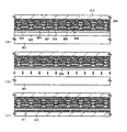
本実施例では、図1、図2に示した構成とは異なる構成により素子が形成された基板を分離する方法について説明する。説明には図10(A)〜図10(C)を用いることとする。
【0090】
まず、図10(A)は角基板を2枚貼り合わせた試料11から素子を形成する際に母体基板として用いたガラス基板を分離する例を示す。なお、試料11には12で示される単位でEL発光装置が形成されている。このEL発光装置の作製方法に関しては実施例1、実施例4を参考にすれば良い。
【0091】
図10(A)の場合、ノズル13が試料11の一辺に沿って平行に移動し、その動きに従って流体14も平行に移動する。即ち、試料11の一辺に沿って流体14が移動することにより剥離層を崩壊させることができる。
【0092】
次に、図10(B)の場合、ノズル13が試料11の一辺に沿って平行に移動し、かつ、ノズル15がノズル13に対向する一辺に沿って平行に移動するように設けられている。そして、各々のノズルの動きに従って流体14、16も平行に移動する。即ち、試料11を挟むように、二辺に沿って流体14、16が移動することにより剥離層を崩壊させることができる。このことはスループットの向上に寄与する。
【0093】
なお、図10(B)の場合において、ノズルは二辺だけでなく、三辺もしくは四辺に設けられても良いし、二辺に設ける場合においても、隣接する辺に設ける構成としても良い。
【0094】
次に、図10(C)の場合、ノズル17が試料11の一辺とほぼ同じ長さの噴射口を有している。即ち、ノズルを移動させることなく試料11の一辺全体に流体18を噴射させることができるため、ノズルの移動機構を設ける必要がなくなる。このことは分離装置の小型化に寄与する。
【0095】
なお、図10(A)〜(C)の図面では、各辺に対応して一つのノズルが設けられた構成を示しているが、一辺につき二つ以上の噴射口を有するノズルを用いることも可能である。
【0096】
〔実施例9〕
本発明を実施して形成された表示装置は様々な電気器具の表示部として用いることができる。そのような本発明の電気器具としては、ビデオカメラ、デジタルカメラ、ゴーグル型ディスプレイ(ヘッドマウントディスプレイ)、カーナビゲーション、カーオーディオ、ノート型パーソナルコンピュータ、ゲーム機器、携帯情報端末(モバイルコンピュータ、携帯電話、携帯型ゲーム機または電子書籍)、記録媒体を備えた画像再生装置(具体的には記録媒体を再生し、その画像を表示しうるディスプレイを備えた装置)などが挙げられる。それら電気器具の具体例を図11に示す。
【0097】
図11(A)はデジタルカメラであり、本体2001、表示部2002、接眼部部2003、操作スイッチ2004を含む。本発明の表示装置は表示部2002に用いることができる。
【0098】
図11(B)は頭部取り付け型のELディスプレイの一部(右片側)であり、本体2101、信号ケーブル2102、頭部固定バンド2103、表示部2104、光学系2105、表示装置2106を含む。本発明は表示装置2106に用いることができる。
【0099】
図11(C)は携帯型(モバイル)コンピュータであり、本体2301、表示部2302、受像部2303、操作スイッチ2304、メモリスロット2305を含む。本発明の表示装置は表示部2302に用いることができる。この携帯型コンピュータはフラッシュメモリや不揮発性メモリを集積化した記録媒体に情報を記録したり、それを再生したりすることができる。
【0100】
図11(D)は電子書籍(携帯書籍)であり、本体2401、表示部2402、操作スイッチ2403を含む。本発明の表示装置は表示部2402に用いることができる。また、この電子書籍に記録媒体を挿入するためのスロットを設けることも可能である。
【0101】
ところで、表示部に対してEL発光装置を用いる場合、EL発光装置は発光している部分が電力を消費するため、発光部分が極力少なくなるように情報を表示することが望ましい。従って、携帯情報端末、特に携帯電話や電子書籍のような文字情報を主とする表示部にEL発光装置を用いる場合には、非発光部分を背景として文字情報を発光部分で形成するように駆動することが望ましい。
【0102】
ここで図11(E)は携帯電話であり、本体2501、音声出力部2502、音声入力部2503、表示部2504、操作スイッチ2505、アンテナ2506を含む。本発明の表示装置は表示部2504に用いることができる。なお、表示部2504にEL発光装置を用いる場合は黒色の背景に白色の文字を表示することで携帯電話の消費電力を抑えることができる。
【0103】
以上の様に、本発明の適用範囲は極めて広く、あらゆる分野の電気器具に用いることが可能である。また、本実施例の電気器具は実施例1〜7の構成を自由に組み合わせた表示装置を用いることで得ることができる。
【0104】
【発明の効果】
本発明では、半導体素子もしくはMIM素子といった能動素子の作製過程において、母体基板としてプラスチックよりも耐熱性の高い基板を用いるため、電気特性の良好な能動素子を作製することができる。さらに、能動素子並びに発光素子もしくは液晶素子を形成した後で前記母体基板を剥離し、プラスチック基板を支持基板として貼り合わせる。
【0105】
そのため、プラスチック基板を支持基板とし、且つ、高性能な表示装置を作製することが可能となる。また、支持基板がプラスチックであるため、フレキシブルな表示装置にすることもでき、且つ、薄型で軽量な表示装置とすることが可能である。
【図面の簡単な説明】
【図1】 基板を分離する過程を断面から見た図。
【図2】 基板を分離する過程を上面から見た図。
【図3】 本発明に用いる分離装置の概略図。
【図4】 EL発光装置の作製工程を示す図。
【図5】 EL発光装置の作製工程を示す図。
【図6】 EL発光装置の上面構造および回路構成を示す図。
【図7】 液晶表示装置の作製工程を示す図。
【図8】 EL発光装置の作製工程を示す図。
【図9】 EL発光装置の作製工程を示す図。
【図10】 基板を分離する過程を上面から見た図。
【図11】 電気器具の一例を示す図。[0001]
BACKGROUND OF THE INVENTION
The present invention relates to a device having an element (hereinafter referred to as a light emitting device) having a luminescent material sandwiched between electrodes (hereinafter referred to as a light emitting device) or a device having an element (hereinafter referred to as liquid crystal element) having a liquid crystal sandwiched between electrodes. The present invention relates to a manufacturing method (hereinafter referred to as a liquid crystal display device). An organic EL display and an organic light emitting diode (OLED) are included in the light emitting device of the present invention.
[0002]
In this specification, the light emitting device and the liquid crystal display device are collectively referred to as a display device (electro-optical device).
[0003]
The luminescent material that can be used in the present invention includes all luminescent materials that emit light (phosphorescence and / or fluorescence) via singlet excitation, triplet excitation, or both excitation.
[0004]
[Prior art]
In recent years, development of a light-emitting device (hereinafter referred to as an EL light-emitting device) using a light-emitting element (hereinafter referred to as an EL element) using a light-emitting material (hereinafter referred to as an EL material) from which EL (Electro Luminescence) can be obtained has progressed. Yes. An EL light emitting device has a structure having an EL element having a structure in which an EL material is sandwiched between an anode and a cathode. By applying a voltage between the anode and the cathode and passing a current through the EL material, carriers are recombined to emit light. That is, since the EL light emitting device has a light emitting capability, the backlight used for the liquid crystal display device is unnecessary. Furthermore, it has the advantages of a wide viewing angle, light weight, and low power consumption.
[0005]
Various applications using such an EL light-emitting device are expected. Especially, the use of the EL light-emitting device in mobile devices is attracting attention because the thickness of the EL light-emitting device is thin, and thus the weight can be reduced. . Therefore, it has been attempted to form a light emitting element on a flexible plastic film.
[0006]
However, since the heat resistance of the plastic film is low, the maximum temperature of the process has to be lowered, and as a result, TFTs having better electrical characteristics cannot be formed than when formed on a glass substrate. Therefore, a high-performance display device using a plastic film has not been realized.
[0007]
[Problems to be solved by the invention]
An object of the present invention is to provide a technique for manufacturing a high-performance display device using a plastic support (including a flexible plastic film or a plastic substrate).
[0008]
[Means for Solving the Problems]
In the present invention, necessary elements are formed on a substrate (glass substrate, quartz substrate, silicon substrate, metal substrate, or ceramic substrate) that is more heat resistant than plastic, and these elements are later processed at room temperature into a plastic substrate. (Including plastic film).
[0009]
Note that the necessary elements refer to semiconductor elements (typically TFTs) or MIM elements and light emitting elements or liquid crystal elements used as pixel switching elements in the case of an active matrix display device. A passive display device refers to a light-emitting element or a liquid crystal element. In the present specification, a semiconductor element or an MIM element is called an active element, and a light emitting element or a liquid crystal element is called a passive element.
[0010]
As the plastic substrate, a substrate or a film made of polyimide, epoxy resin, acrylic resin, PES (polyethylene sulfide), PC (polycarbonate), PET (polyethylene terephthalate) or PEN (polyethylene naphthalate) can be used.
[0011]
In the present invention, the element is formed on a release layer, and a substrate on which the element is formed is separated by spraying a fluid toward the release layer, and a plastic substrate is newly attached. Yes. As the separation layer, a porous silicon layer or a silicon layer to which hydrogen, oxygen, nitrogen, or a rare gas is added is used.
[0012]
In addition, as a method of spraying the fluid, a method of spraying and blowing a high-pressure water stream from a nozzle (referred to as a water jet method) or a method of spraying and spraying a high-pressure gas stream can be used. At this time, an organic solvent, an acidic solution or an alkaline solution may be used instead of water. As the gas, air, nitrogen gas, carbon dioxide gas or rare gas may be used, or these gases may be converted into plasma.
[0013]
When these fluids are sprayed onto the release layer, the release layer collapses due to brittleness or is chemically removed. As a result, the substrate on which the element is formed is separated from the insulating film provided as the base of the element. When separated by the collapse of the release layer, the remaining release layer may be removed again by etching.
[0014]
In this way, the insulating film which becomes the base of the element is exposed, and a new plastic substrate or film is attached. When pasting, a photocurable resin, a thermosetting resin, or an epoxy resin can be used as an adhesive.
[0015]
As described above, in the present invention, first, an active element such as a semiconductor element or MIM element or a passive element such as a light emitting element or a liquid crystal element is formed on a substrate (element formation substrate) having higher heat resistance than plastic, and finally the element formation is performed. Replace the substrate with a plastic substrate. It is characterized in that the substrate is separated using high-pressure water or high-pressure gas during the replacement.
[0016]
Further, as means for separating the composite member by blowing a high-pressure fluid onto the side surface of the composite member and an apparatus therefor, JP-A-11-45840, JP-A-11-5064, JP-A-11-195563 are disclosed. JP-A-11-195568, JP-A-11-195568, and JP-A-11-195570 can be cited in the present invention.
[0017]
DETAILED DESCRIPTION OF THE INVENTION
Embodiments of the present invention will be described. FIG. 1 is a schematic view of the present invention, in which 101 is a glass substrate, 102 is a peeling layer, 103 is an underlying insulating film, 104 is an element formed on the insulating film 103, 105 is an insulating film made of resin, 106 Is a plastic film.
[0018]
The
[0019]
The insulating film 103 may be an insulating film containing silicon. As the insulating film containing silicon, a silicon oxide film, a silicon nitride film, a silicon nitride oxide film, or a silicon carbide film can be used. Further, the element 104 formed thereon may be a combination of an active element such as a semiconductor element or an MIM element and a passive element such as a light emitting element or a liquid crystal element, or may be a light emitting element or a liquid crystal element. .
[0020]
The insulating film 105 made of resin has both a role as a sealing material for protecting the element 104 from the outside air and a role as an adhesive for attaching the
[0021]
The display device including the above structure is rotated as indicated by an arrow about the center, and the fluid 108 is ejected from the nozzle 107. 1 × 10 from nozzle 107 7 ~ 1x10 9 Pa (preferably 3 × 10 7 ~ 5x10 8 A fluid to which a pressure of Pa) is applied is jetted and sprayed onto the side surface of the
[0022]
Note that the fluid 108 may be a liquid such as water, an organic solvent, an acidic solution, or an alkaline solution, or may be a gas such as air, nitrogen gas, carbon dioxide gas, or rare gas. Further, these gases may be converted into plasma.
[0023]
FIG. 2 shows the state of FIG. 1 when viewed from above. Note that FIG. 2A illustrates a sample 201 using a round substrate as a base substrate for forming an element. A display device is formed in the sample 201 in units indicated by 202. This is an example of manufacturing a plurality of display devices from a single substrate. Similarly, FIG. 2B shows a sample 203 using a square substrate, and a display device is formed on the sample 203 in units indicated by 204.
[0024]
At this time, the ejection port of the nozzle 107 has an elliptical shape or a rectangular shape, and the cross-sectional shape of the fluid 108 substantially matches the shape of the nozzle. A circular shape or a quadrangular shape may be used, but the processing efficiency is higher when the shape is an oblong shape or a rectangular shape.
[0025]
Although only one nozzle is shown here, two or more nozzles may be provided. At that time, a plurality of the substrates may be provided side by side, or one or more nozzles may be provided for each side of the substrate.
[0026]
Next, FIG. 3 shows a schematic structure of an apparatus for ejecting the fluid 108 (hereinafter referred to as a separation apparatus) in the present invention. In the separation apparatus shown in FIG. 3, a sample 301 having a structure as shown in FIG. 1 is held by substrate holders 302 and 303. The substrate holders 302 and 303 each hold the sample 301 by vacuum suction.
[0027]
Further, the substrate holders 302 and 303 are arranged on the same rotation axis so as to be rotatable. In addition, the substrate holder 302 is fitted to the bearings 304 and 305 and supported by the support base 306. Further, the substrate holder 302 is connected to a motor 307 so that the rotation speed can be adjusted.
[0028]
On the other hand, the substrate holder 303 is fitted to the bearings 308 and 309 and supported by the support base 310. Further, the substrate holder 303 is pulled rightward by the compression spring 311, and the sample 301 is held by balancing the force and the adsorption force of the substrate holder 303.
[0029]
In this state, a high-pressure fluid is sent from the pump 315 to the nozzle 316, and the fluid 317 is jetted toward the
[0030]
Thus, when the fluid 317 is sprayed on the
[0031]
Note that although an example in which the sample 301 is rotated is shown in the embodiment of the present invention, a configuration in which the nozzle 316 rotates along the side surface of the sample 301 and jets a high-pressure fluid is also possible.
[0032]
【Example】
[Example 1]
In this embodiment, a manufacturing process of a pixel portion of an EL light-emitting device will be described with reference to FIGS. A top view of a pixel manufactured according to this embodiment mode is shown in FIG. The reference numerals used in FIG. 6 correspond to the reference numerals used in FIGS.
[0033]
First, a
[0034]
Next, a silicon nitride oxide film is formed as a
[0035]
Next, a
[0036]
Next, as shown in FIG. 4B, patterned
[0037]
Then, an element (typically boron) belonging to Group 13 of the periodic table is added using the
[0038]
Next, as shown in FIG. 4C, a
[0039]
When the activation is completed, it is effective to perform a hydrogenation treatment. For the hydrogenation treatment, a known hydrogen annealing technique or plasma hydrogenation technique may be used.
[0040]
Next, as shown in FIG. 4D, a first
[0041]
In this state, the switching
[0042]
At the same time, a
[0043]
Next, as shown in FIG. 4E, an oxide conductive film (a conductive film obtained by adding gallium oxide to zinc oxide in this embodiment) is formed to a thickness of 100 nm, and a
[0044]
After the
[0045]
In this embodiment, CuPc (copper phthalocyanine) is used as the hole injection layer. In this case, first, copper phthalocyanine is formed so as to cover all the pixel electrodes, and then a red light emitting layer, a green light emitting layer, and a blue light emitting layer are formed for each pixel corresponding to red, green, and blue. The regions to be formed may be distinguished using a shadow mask during vapor deposition. In this way, color display is possible.
[0046]
In this embodiment, Alq is used as the base material of the green light emitting layer. Three (Tris-8-quinolinolato aluminum complex) is used and quinacridone or coumarin 6 is added as a dopant. Further, Alq as a base material of the red light emitting layer Three And DCJT, DCM1 or DCM2 is added as a dopant. Further, as a base material of the blue light emitting layer, BAlq Three (5-coordinate complex having a mixed ligand of 2-methyl-8-quinolinol and a phenol derivative) and perylene is added as a dopant.
[0047]
Of course, in the present invention, it is not necessary to limit to the above organic material, and it is possible to use a known low molecular organic EL material, high molecular organic EL material or inorganic EL material. When using a polymer organic EL material, a coating method can also be used.
[0048]
As described above, an EL element (indicated by 602 in FIG. 6B) including the pixel electrode (anode) 424, the organic EL layer 427, and the
[0049]
Next, as illustrated in FIG. 5A, a
[0050]
By performing the process of FIG. 5A, the EL element can be completely shielded from the atmosphere. Thereby, deterioration of the organic EL material due to oxidation can be suppressed almost completely, and the reliability of the EL element can be greatly improved.
[0051]
Next, as shown in FIG. 5B, the
[0052]
When the TFT and the EL element are transferred to the
[0053]
Thus, the TFT and the EL element are transferred from the
[0054]
In this embodiment, the reason why the supporting
[0055]
In addition, the EL light-emitting device manufactured according to this embodiment has a very small number of masks necessary for photolithography, which is 6 in total, and can achieve a high yield and a low manufacturing cost. In addition, the EL light-emitting device formed in this way can have high performance because a TFT formed without being limited by the heat resistance of the plastic substrate can be used as an active element.
[0056]
In this embodiment, a TFT with a top gate structure (specifically, a planar TFT) is shown as an example of a TFT, but a TFT with a bottom gate structure (typically an inverted staggered TFT) may be used.
[0057]
[Example 2]
In Example 1, the manufacturing process up to the formation of the gate electrode is disclosed in Japanese Patent Application Laid-Open No. 9-31260, Japanese Patent Application Laid-Open No. 10-247735, Japanese Patent Application Laid-Open No. 10-270363, or Japanese Patent Application Laid-Open No. 11-191628. It is effective to use the invention described in any of the publications.
[0058]
All of the techniques described in the above publications are techniques for forming a crystalline silicon film having very high crystallinity, and high performance TFTs can be formed by using these techniques. All of these techniques include heat treatment at 550 ° C. or higher, but by using the technique of the present invention, it becomes possible to use a plastic substrate having low heat resistance as the element formation substrate.
[0059]
The configuration of the present embodiment can be implemented by freely combining with the configuration of the first embodiment.
[0060]
Example 3
In this embodiment, an example in which the present invention is used in a liquid crystal display device will be described. FIG. 7 is used for the description.
[0061]
In FIG. 7A, 701 is a glass substrate and 702 is an amorphous silicon layer. 16 ~ 1x10 17 atoms / cm Three A separation layer containing hydrogen at a concentration of 703, a base film made of a silicon nitride oxide film, and 704 a pixel TFT. The
[0062]
The manufacturing process described in Embodiment 1 may be followed up to the structure described above. Needless to say, the structure of the TFT can be a bottom gate type (typically an inverted staggered type), and the TFT manufacturing process is not necessarily limited to the process of the first embodiment.
[0063]
After the
[0064]
Next, a
[0065]
Next, a sealing material (not shown) is formed on the
[0066]
Next, as illustrated in FIG. 7B, the
[0067]
After that, the
[0068]
Thus, finally, the
[0069]
As described above, when the present invention is used for a liquid crystal display device, the liquid crystal injection device is completed by completing the liquid crystal injection step, and then the peeling layer removing step is performed while fixing the element with the counter substrate. Can do. Therefore, a high-performance TFT can be formed on a plastic substrate without increasing particularly complicated processes. It is possible to combine the configuration of the second embodiment with the configuration of the second embodiment.
[0070]
Example 4
In this embodiment, an example in which the present invention is used in a simple matrix EL light emitting device will be described. FIG. 8 is used for the description.
[0071]
In FIG. 8A, 801 is a glass substrate, 802 is a release layer made of a porous silicon film, 803 is a base film made of a silicon oxide film, and 804 is a first stripe electrode. An anode made of a film. A plurality of
[0072]
On the
[0073]
These are formed so as to be orthogonal to the
[0074]
At this time, a capacitor formed by the
[0075]
After the EL element is formed, the
[0076]
Next, the substrate over which the EL element is formed is exposed to a nitrogen atmosphere containing chlorine trifluoride gas, and the
[0077]
The EL light-emitting device manufactured according to this example has a very small number of masks necessary for photolithography, which is two in total, and can achieve a high yield and a low manufacturing cost. Further, an external IC chip or a drive circuit (stick driver) described in JP-A-8-262474 may be used as a drive circuit for inputting signals to the anode and the cathode. In addition, the configuration of the present embodiment can be implemented in combination with the second embodiment.
[0078]
Example 5
In this embodiment, an example in which a color filter is provided in advance on a plastic substrate to be bonded last is shown. Note that although a passive matrix EL light emitting device is described as an example in this embodiment, the present invention can also be applied to an active matrix EL light emitting device.
[0079]
First, the state shown in FIG. 8B is obtained according to the fourth embodiment. However, in this embodiment, a white light emitting organic EL layer 900 is formed instead of the
[0080]
Then, a color filter (R) (a color filter for extracting red light) 901, a color filter (G) (a color filter for extracting green light) 902, and a color filter (B) (a color filter for extracting blue light) 903 in advance. The plastic film 904 provided with is bonded with an adhesive 905 made of resin.
[0081]
At this time, each of the color filters 901 to 903 can be formed on the plastic film 904 without any problem because it can be formed using a spin coating method, a combination of an inkjet method and a photolithography technique, or a printing method. (Fig. 9 (B))
[0082]
In the case of this embodiment, white light emitted from the organic EL layer 900 is passed through the color filters 901 to 903 to extract red light, green light, or blue light. This method has an advantage that the manufacturing process is simplified because the organic EL layer only needs to be formed once. The configuration of the present embodiment can be implemented in combination with the configurations of the first to third embodiments.
[0083]
Example 6
In the present invention, it is effective to form a carbon film, preferably a DLC (diamond-like carbon) film, on one or both sides of a substrate for fixing elements and / or a plastic substrate for bonding. However, if the film thickness is too thick, the transmittance decreases, so the film thickness is preferably 50 nm or less (preferably 10 to 20 nm).
[0084]
As a feature of the DLC film, 1550cm -1 1300cm with asymmetric peaks -1 It has a Raman spectral distribution with shoulders. Moreover, it has the characteristic of showing a hardness of 15 to 25 GPa when measured with a micro hardness meter. Such a DLC film has higher hardness than a plastic support, and it is effective to provide it as a protective film for surface protection.
[0085]
Further, the DLC film has a high passivation effect against moisture and oxygen, and has a property of not transmitting these. Therefore, it is particularly effective when a light emitting element using an organic EL layer that is weak against moisture and oxygen is formed.
[0086]
The DLC film can be formed in advance before the plastic substrate is attached, or can be formed after the plastic substrate is attached. In any case, the DLC film may be formed by sputtering or ECR plasma CVD.
[0087]
In addition, the structure of a present Example can be implemented in combination with any structure of Examples 1-5 freely.
[0088]
Example 7
In Examples 1, 2, and 4-6, the display device using an EL element as a light emitting element has been described as an example. However, the present invention is not limited to an EC (electrochromic) display device, a field emission display (FED), or a semiconductor. It can also be used for a display device having the used light emitting diode.
[0089]
Example 8
In this embodiment, a method for separating a substrate on which an element is formed with a structure different from the structure shown in FIGS. 10A to 10C are used for the description.
[0090]
First, FIG. 10A shows an example of separating a glass substrate used as a base substrate when an element is formed from a sample 11 in which two square substrates are bonded together. Note that an EL light emitting device is formed on the sample 11 in units indicated by 12. Regarding the manufacturing method of this EL light emitting device, Embodiments 1 and 4 may be referred to.
[0091]
In the case of FIG. 10A, the nozzle 13 moves in parallel along one side of the sample 11, and the fluid 14 also moves in parallel according to the movement. That is, the release layer can be collapsed by the fluid 14 moving along one side of the sample 11.
[0092]
Next, in the case of FIG. 10B, the nozzle 13 is provided to move in parallel along one side of the sample 11, and the nozzle 15 is provided to move in parallel along one side facing the nozzle 13. . The fluids 14 and 16 also move in parallel according to the movement of each nozzle. That is, the release layer can be collapsed by moving the fluids 14 and 16 along two sides so as to sandwich the sample 11. This contributes to an improvement in throughput.
[0093]
In the case of FIG. 10B, the nozzles may be provided not only on the two sides but also on the three or four sides, and when provided on the two sides, the nozzles may be provided on the adjacent sides.
[0094]
Next, in the case of FIG. 10C, the
[0095]
10A to 10C show a configuration in which one nozzle is provided corresponding to each side, a nozzle having two or more injection ports per side may be used. Is possible.
[0096]
Example 9
A display device formed by implementing the present invention can be used as a display portion of various electric appliances. As such an electric appliance of the present invention, a video camera, a digital camera, a goggle type display (head mounted display), a car navigation system, a car audio, a notebook type personal computer, a game machine, a personal digital assistant (mobile computer, mobile phone, A portable game machine or an electronic book), an image playback device provided with a recording medium (specifically, a device provided with a display capable of playing back the recording medium and displaying the image), and the like. Specific examples of these electric appliances are shown in FIG.
[0097]
FIG. 11A illustrates a digital camera, which includes a
[0098]
FIG. 11B shows a part (right side) of a head-mounted EL display, which includes a main body 2101, a signal cable 2102, a
[0099]
FIG. 11C illustrates a portable (mobile) computer, which includes a
[0100]
FIG. 11D illustrates an electronic book (mobile book) which includes a
[0101]
By the way, when an EL light-emitting device is used for the display unit, the EL light-emitting device consumes power in the light-emitting portion, and thus it is desirable to display information so that the light-emitting portion is minimized. Therefore, when an EL light emitting device is used in a display unit mainly including character information such as a portable information terminal, particularly a mobile phone or an electronic book, the character information is driven to form the light emitting part with the non-light emitting part as the background. It is desirable to do.
[0102]
Here, FIG. 11E illustrates a mobile phone, which includes a
[0103]
As described above, the application range of the present invention is extremely wide and can be used for electric appliances in various fields. Moreover, the electric appliance of a present Example can be obtained by using the display apparatus which combined the structure of Examples 1-7 freely.
[0104]
【Effect of the invention】
In the present invention, since a substrate having higher heat resistance than plastic is used as a base substrate in the process of manufacturing an active element such as a semiconductor element or an MIM element, an active element having excellent electrical characteristics can be manufactured. Further, after forming the active element and the light emitting element or the liquid crystal element, the base substrate is peeled off, and a plastic substrate is attached as a supporting substrate.
[0105]
Therefore, a high-performance display device can be manufactured using a plastic substrate as a support substrate. Further, since the supporting substrate is made of plastic, a flexible display device can be obtained, and a thin and light display device can be obtained.
[Brief description of the drawings]
FIG. 1 is a cross-sectional view of a process of separating a substrate.
FIG. 2 is a top view of a process of separating a substrate.
FIG. 3 is a schematic view of a separation apparatus used in the present invention.
4A and 4B illustrate a manufacturing process of an EL light-emitting device.
FIGS. 5A and 5B illustrate a manufacturing process of an EL light-emitting device. FIGS.
6A and 6B are a top view and a circuit configuration of an EL light emitting device.
FIGS. 7A to 7C illustrate a manufacturing process of a liquid crystal display device. FIGS.
FIG. 8 illustrates a manufacturing process of an EL light-emitting device.
FIGS. 9A and 9B illustrate a manufacturing process of an EL light-emitting device. FIGS.
FIG. 10 is a top view of a process of separating a substrate.
FIG. 11 illustrates an example of an electric appliance.
Claims (12)
前記剥離層の上に絶縁膜を形成し、
前記絶縁膜の上に第1の電極を形成し、
前記第1の電極上に発光層を形成し、
前記発光層上に第2の電極を形成し、
前記第2の電極の上方に第2の基板を貼り合わせ、
前記第2の基板を貼り合わせた後に前記剥離層に対して流体を噴射し、前記第1の基板と前記絶縁膜とを分離し、
前記絶縁膜にプラスチックからなる第3の基板を貼り合わせることを特徴とする発光装置の作製方法。Forming a release layer on the first substrate;
An insulating film is formed on the peeling layer,
A first electrode formed on the insulating film,
Forming a light emitting layer on the first electrode;
Forming a second electrode on the light emitting layer;
A second substrate is bonded above the second electrode ,
The fluid ejected against the release layer, and separating the insulating film and the first substrate after bonding the second substrate,
A method for manufacturing a light-emitting device , wherein a third substrate made of plastic is attached to the insulating film.
前記剥離層の上に絶縁膜を形成し、Forming an insulating film on the release layer;
前記絶縁膜の上にTFTを形成し、A TFT is formed on the insulating film,
前記TFTの上に前記TFTと電気的に接続されている第1の電極を形成し、Forming a first electrode electrically connected to the TFT on the TFT;
前記第1の電極上に発光層を形成し、Forming a light emitting layer on the first electrode;
前記発光層上に第2の電極を形成し、Forming a second electrode on the light emitting layer;
前記第2の電極の上方に第2の基板を貼り合わせ、A second substrate is bonded above the second electrode,
前記第2の基板を貼り合わせた後に前記剥離層に対して流体を噴射し、前記第1の基板と前記絶縁膜とを分離し、After laminating the second substrate, a fluid is sprayed onto the release layer to separate the first substrate and the insulating film;
前記絶縁膜にプラスチックからなる第3の基板を貼り合わせることを特徴とする発光装置の作製方法。A method for manufacturing a light-emitting device, wherein a third substrate made of plastic is attached to the insulating film.
前記剥離層は多孔質シリコン膜であることを特徴とする発光装置の作製方法。The method for manufacturing a light-emitting device, wherein the release layer is a porous silicon film.
前記流体は圧力が加えられた液体もしくは気体であること特徴とする発光装置の作製方法。The method for manufacturing a light-emitting device, wherein the fluid is a liquid or a gas under pressure.
前記第2の基板はプラスチックであることを特徴とする発光装置の作製方法。The method for manufacturing a light-emitting device, wherein the second substrate is plastic.
前記第2の基板及び前記第3の基板はプラスチックフィルムであることを特徴とする発光装置の作製方法。The method for manufacturing a light-emitting device, wherein the second substrate and the third substrate are plastic films.
前記剥離層の上に絶縁膜を形成し、
前記絶縁膜の上方にTFTを形成し、
前記TFTの上に前記TFTと電気的に接続されている第1の電極を形成し、
第2の電極を有する第2の基板を前記第1の電極に向かい合わせるように貼り合わせ、
前記第1の電極と前記第2の電極との間に液晶を注入し、
前記液晶を注入後に前記剥離層に対して流体を噴射し、前記第1の基板と前記絶縁膜とを分離し、
前記絶縁膜にプラスチックからなる第3の基板を貼り合わせることを特徴とする表示装置の作製方法。Forming a release layer on the first substrate;
An insulating film is formed on the peeling layer,
A TFT is formed above the insulating film;
Forming a first electrode electrically connected to the TFT on the TFT;
A second substrate having a second electrode is bonded to face the first electrode,
Injecting liquid crystal between the first electrode and the second electrode;
After injecting the liquid crystal, a fluid is sprayed on the release layer, and the first substrate and the insulating film are separated,
A method for manufacturing a display device, wherein a third substrate made of plastic is bonded to the insulating film.
前記剥離層は非晶質シリコン膜を陽極化成することにより形成されることを特徴とする表示装置の作製方法。 In claim 7,
The method for manufacturing a display device, wherein the release layer is formed by anodizing an amorphous silicon film.
前記剥離層は多孔質シリコン膜であることを特徴とする表示装置の作製方法。 In claim 7 or claim 8,
The method for manufacturing a display device, wherein the release layer is a porous silicon film.
前記流体は圧力が加えられた液体もしくは気体であること特徴とする表示装置の作製方法。 In any one of Claims 7 to 9,
The method for manufacturing a display device, wherein the fluid is a liquid or a gas under pressure.
前記第2の基板はプラスチックであることを特徴とする表示装置の作製方法。 In any one of Claims 7 to 10,
The method for manufacturing a display device, wherein the second substrate is made of plastic.
前記第2の基板及び前記第3の基板はプラスチックフィルムであることを特徴とする表示装置の作製方法。The method for manufacturing a display device, wherein the second substrate and the third substrate are plastic films.
Priority Applications (1)
| Application Number | Priority Date | Filing Date | Title |
|---|---|---|---|
| JP2001072959A JP4884592B2 (en) | 2000-03-15 | 2001-03-14 | Method for manufacturing light emitting device and method for manufacturing display device |
Applications Claiming Priority (4)
| Application Number | Priority Date | Filing Date | Title |
|---|---|---|---|
| JP2000071673 | 2000-03-15 | ||
| JP2000071673 | 2000-03-15 | ||
| JP2000-71673 | 2000-03-15 | ||
| JP2001072959A JP4884592B2 (en) | 2000-03-15 | 2001-03-14 | Method for manufacturing light emitting device and method for manufacturing display device |
Publications (3)
| Publication Number | Publication Date |
|---|---|
| JP2001331120A JP2001331120A (en) | 2001-11-30 |
| JP2001331120A5 JP2001331120A5 (en) | 2009-08-20 |
| JP4884592B2 true JP4884592B2 (en) | 2012-02-29 |
Family
ID=26587530
Family Applications (1)
| Application Number | Title | Priority Date | Filing Date |
|---|---|---|---|
| JP2001072959A Expired - Fee Related JP4884592B2 (en) | 2000-03-15 | 2001-03-14 | Method for manufacturing light emitting device and method for manufacturing display device |
Country Status (1)
| Country | Link |
|---|---|
| JP (1) | JP4884592B2 (en) |
Families Citing this family (53)
| Publication number | Priority date | Publication date | Assignee | Title |
|---|---|---|---|---|
| JPS6444420A (en) * | 1987-08-11 | 1989-02-16 | Fujitsu Ltd | Opposed matrix type tft panel |
| TW494447B (en) | 2000-02-01 | 2002-07-11 | Semiconductor Energy Lab | Semiconductor device and manufacturing method thereof |
| US7579203B2 (en) | 2000-04-25 | 2009-08-25 | Semiconductor Energy Laboratory Co., Ltd. | Light emitting device |
| TW519852B (en) * | 2001-10-18 | 2003-02-01 | Opto Tech Corp | Organic light emitting device capable of projecting white light source and its manufacturing method |
| KR100611018B1 (en) * | 2001-12-05 | 2006-08-09 | 옵토 테크 코포레이션 | White light emitting organic electroluminescent device and method for fabricating the same |
| JP2003255858A (en) * | 2002-02-28 | 2003-09-10 | Sanyo Electric Co Ltd | Display device |
| JP3838964B2 (en) | 2002-03-13 | 2006-10-25 | 株式会社リコー | Functional element substrate manufacturing equipment |
| JP2005000914A (en) * | 2002-03-13 | 2005-01-06 | Ricoh Co Ltd | Manufacturing apparatus of functional element substrate |
| JP3957535B2 (en) | 2002-03-14 | 2007-08-15 | 株式会社半導体エネルギー研究所 | Driving method of light emitting device, electronic device |
| JP2004071874A (en) | 2002-08-07 | 2004-03-04 | Sharp Corp | Semiconductor device manufacturing method and semiconductor device |
| JP2004140267A (en) | 2002-10-18 | 2004-05-13 | Semiconductor Energy Lab Co Ltd | Semiconductor device and fabrication method thereof |
| CN100391004C (en) | 2002-10-30 | 2008-05-28 | 株式会社半导体能源研究所 | Semiconductor device and manufacturing method thereof |
| JP2004207078A (en) * | 2002-12-25 | 2004-07-22 | Seiko Epson Corp | Display panel and method for manufacturing display panel |
| JP4373085B2 (en) | 2002-12-27 | 2009-11-25 | 株式会社半導体エネルギー研究所 | Semiconductor device manufacturing method, peeling method, and transfer method |
| KR101033797B1 (en) | 2003-01-15 | 2011-05-13 | 가부시키가이샤 한도오따이 에네루기 켄큐쇼 | Separating method and method for manufacturing display device using the separating method |
| JP4801579B2 (en) * | 2003-01-15 | 2011-10-26 | 株式会社半導体エネルギー研究所 | Method for manufacturing light emitting device |
| JP4566578B2 (en) * | 2003-02-24 | 2010-10-20 | 株式会社半導体エネルギー研究所 | Method for manufacturing thin film integrated circuit |
| US7973313B2 (en) | 2003-02-24 | 2011-07-05 | Semiconductor Energy Laboratory Co., Ltd. | Thin film integrated circuit device, IC label, container comprising the thin film integrated circuit, manufacturing method of the thin film integrated circuit device, manufacturing method of the container, and management method of product having the container |
| JP2004281085A (en) * | 2003-03-12 | 2004-10-07 | Nippon Hoso Kyokai <Nhk> | Flexible organic el device and flexible organic el display |
| JP4526771B2 (en) | 2003-03-14 | 2010-08-18 | 株式会社半導体エネルギー研究所 | Method for manufacturing semiconductor device |
| JP3897173B2 (en) | 2003-05-23 | 2007-03-22 | セイコーエプソン株式会社 | Organic EL display device and manufacturing method thereof |
| KR100615028B1 (en) | 2004-02-27 | 2006-08-22 | 한성엘컴텍 주식회사 | Key Pad having enhanced adhesive between EL Device and silicon and EL Device used to the same |
| TWI413152B (en) | 2005-03-01 | 2013-10-21 | Semiconductor Energy Lab | Manufacturing method of semiconductor device |
| WO2006104019A1 (en) | 2005-03-28 | 2006-10-05 | Semiconductor Energy Laboratory Co., Ltd. | Semiconductor device, manufacturing method thereof, and measuring method thereof |
| JP2007096288A (en) * | 2005-08-31 | 2007-04-12 | Sumitomo Chemical Co Ltd | Transistor and method of manufacturing same, and semiconductor device having the same |
| JP4781082B2 (en) * | 2005-10-24 | 2011-09-28 | 株式会社半導体エネルギー研究所 | Method for manufacturing semiconductor device |
| WO2008018026A2 (en) * | 2006-08-10 | 2008-02-14 | Koninklijke Philips Electronics N.V. | Active matrix displays and other electronic devices having plastic substrates |
| TWI450387B (en) | 2006-09-29 | 2014-08-21 | Semiconductor Energy Lab | Method for manufacturing semiconductor device |
| US8137417B2 (en) | 2006-09-29 | 2012-03-20 | Semiconductor Energy Laboratory Co., Ltd. | Peeling apparatus and manufacturing apparatus of semiconductor device |
| EP1970952A3 (en) | 2007-03-13 | 2009-05-06 | Semiconductor Energy Laboratory Co., Ltd. | Semiconductor device and manufacturing method thereof |
| EP1970951A3 (en) | 2007-03-13 | 2009-05-06 | Semiconductor Energy Laboratory Co., Ltd. | Semiconductor device and manufacturing method thereof |
| EP1976001A3 (en) | 2007-03-26 | 2012-08-22 | Semiconductor Energy Laboratory Co., Ltd. | Method for manufacturing semiconductor device |
| EP1976000A3 (en) | 2007-03-26 | 2009-05-13 | Semiconductor Energy Laboratory Co., Ltd. | Method for manufacturing semiconductor device |
| JP2009205669A (en) | 2008-01-31 | 2009-09-10 | Semiconductor Energy Lab Co Ltd | Semiconductor device |
| JP2010041045A (en) | 2008-07-09 | 2010-02-18 | Semiconductor Energy Lab Co Ltd | Semiconductor device and method for producing the same |
| JP5586920B2 (en) | 2008-11-20 | 2014-09-10 | 株式会社半導体エネルギー研究所 | Method for manufacturing flexible semiconductor device |
| KR101824425B1 (en) | 2008-12-17 | 2018-02-02 | 가부시키가이샤 한도오따이 에네루기 켄큐쇼 | Light-emitting device and electronic device |
| CN102460722B (en) | 2009-06-05 | 2015-04-01 | 株式会社半导体能源研究所 | Photoelectric conversion device and method for manufacturing the same |
| TWI517268B (en) | 2009-08-07 | 2016-01-11 | 半導體能源研究所股份有限公司 | Method for manufacturing terminal structure and method for manufacturing electronic device |
| JP5719560B2 (en) | 2009-10-21 | 2015-05-20 | 株式会社半導体エネルギー研究所 | Manufacturing method of terminal structure |
| JP6182307B2 (en) * | 2012-10-16 | 2017-08-16 | リコーインダストリアルソリューションズ株式会社 | Organic EL composite optical element |
| KR101802558B1 (en) | 2013-04-09 | 2017-11-29 | 주식회사 엘지화학 | Method for manufacturing display device and display device manufactured by using same |
| WO2014188636A1 (en) * | 2013-05-21 | 2014-11-27 | シャープ株式会社 | Method for manufacturing display apparatus, display apparatus, and film device |
| TWI695525B (en) | 2014-07-25 | 2020-06-01 | 日商半導體能源研究所股份有限公司 | Separation method, light-emitting device, module, and electronic device |
| CN105702879B (en) * | 2014-11-27 | 2017-08-25 | 上海和辉光电有限公司 | The preparation method of flexible display |
| JP6154442B2 (en) * | 2015-08-19 | 2017-06-28 | 株式会社半導体エネルギー研究所 | Light emitting device |
| CN105702625B (en) * | 2016-04-12 | 2017-11-03 | 武汉华星光电技术有限公司 | The stripping means of flexible base board |
| CN106066550A (en) * | 2016-07-28 | 2016-11-02 | 武汉华星光电技术有限公司 | Liquid crystal display, display panels and preparation method thereof |
| JP6297654B2 (en) * | 2016-09-29 | 2018-03-20 | 株式会社半導体エネルギー研究所 | Light emitting device |
| KR102650013B1 (en) * | 2016-10-05 | 2024-03-21 | 삼성디스플레이 주식회사 | Disassembling system for display device and method for disassembling using this |
| JP2018073835A (en) * | 2017-11-01 | 2018-05-10 | 株式会社半導体エネルギー研究所 | Light-emitting device |
| CN110969931B (en) * | 2018-09-29 | 2022-08-23 | 杰宜斯科技有限公司 | Reworking device and method for display module |
| JP2020024425A (en) * | 2019-09-26 | 2020-02-13 | 株式会社半導体エネルギー研究所 | Light-emitting device |
Family Cites Families (6)
| Publication number | Priority date | Publication date | Assignee | Title |
|---|---|---|---|---|
| JPS61262782A (en) * | 1985-05-17 | 1986-11-20 | 日本電信電話株式会社 | Display unit and making thereof |
| JP3199964B2 (en) * | 1994-10-07 | 2001-08-20 | シャープ株式会社 | Substrate peeling device |
| JPH08274375A (en) * | 1995-03-30 | 1996-10-18 | Sharp Corp | Porous semiconductor light emitting element, and its manufacture |
| JP4146526B2 (en) * | 1997-02-27 | 2008-09-10 | セイコーエプソン株式会社 | Manufacturing method of liquid crystal display device |
| JPH1126733A (en) * | 1997-07-03 | 1999-01-29 | Seiko Epson Corp | Transfer method of thin film device, thin film device, thin film integrated circuit device, active matrix substrate, liquid crystal display and electronic equipment |
| JPH11195568A (en) * | 1997-12-26 | 1999-07-21 | Canon Inc | Specimen separating device, method and manufacture of substrate |
-
2001
- 2001-03-14 JP JP2001072959A patent/JP4884592B2/en not_active Expired - Fee Related
Also Published As
| Publication number | Publication date |
|---|---|
| JP2001331120A (en) | 2001-11-30 |
Similar Documents
| Publication | Publication Date | Title |
|---|---|---|
| JP4884592B2 (en) | Method for manufacturing light emitting device and method for manufacturing display device | |
| JP6837510B2 (en) | Electronics | |
| JP7169414B2 (en) | Method for manufacturing light-emitting device | |
| JP6977194B2 (en) | Electronics | |
| JP4748859B2 (en) | Method for manufacturing light emitting device | |
| US7862677B2 (en) | Display device and method of manufacturing the same | |
| TW480722B (en) | Manufacturing method of electro-optical device | |
| US7491590B2 (en) | Method for manufacturing thin film transistor in display device | |
| KR20030074271A (en) | Light emitting apparatus and method of fabricating the same | |
| JP2016224427A (en) | Method for manufacturing display device and method for manufacturing electronic device | |
| JP4225237B2 (en) | ORGANIC EL DEVICE, METHOD FOR MANUFACTURING ORGANIC EL DEVICE, AND ELECTRONIC DEVICE | |
| KR100712630B1 (en) | Organic electroluminescent device, method of manufacture thereof and electronic apparatus | |
| CN1893145B (en) | Method for manufacturing light emitting device | |
| US20030214247A1 (en) | Light emitting device and a method of manufacturing the same | |
| JP4637391B2 (en) | Method for manufacturing light emitting device | |
| JP4651916B2 (en) | Method for manufacturing light emitting device | |
| KR20030077430A (en) | Light emitting device and method of manufacturing the same | |
| JP2003100450A (en) | Light emitting equipment and its producing method | |
| JP4601843B2 (en) | Light emitting device | |
| JP2003086359A (en) | Light emitting device and electronic device | |
| JP4637390B2 (en) | Method for manufacturing light emitting device | |
| JP4837227B2 (en) | Deposition equipment | |
| JP4610173B2 (en) | Method for manufacturing thin film transistor | |
| JP4657173B2 (en) | Thin film transistor | |
| JP2003109756A (en) | Manufacturing method of illumination device |
Legal Events
| Date | Code | Title | Description |
|---|---|---|---|
| A521 | Request for written amendment filed |
Free format text: JAPANESE INTERMEDIATE CODE: A523 Effective date: 20080207 |
|
| A621 | Written request for application examination |
Free format text: JAPANESE INTERMEDIATE CODE: A621 Effective date: 20080207 |
|
| A521 | Request for written amendment filed |
Free format text: JAPANESE INTERMEDIATE CODE: A523 Effective date: 20090706 |
|
| A977 | Report on retrieval |
Free format text: JAPANESE INTERMEDIATE CODE: A971007 Effective date: 20110201 |
|
| A131 | Notification of reasons for refusal |
Free format text: JAPANESE INTERMEDIATE CODE: A131 Effective date: 20110315 |
|
| A521 | Request for written amendment filed |
Free format text: JAPANESE INTERMEDIATE CODE: A523 Effective date: 20110426 |
|
| TRDD | Decision of grant or rejection written | ||
| A01 | Written decision to grant a patent or to grant a registration (utility model) |
Free format text: JAPANESE INTERMEDIATE CODE: A01 Effective date: 20111206 |
|
| A01 | Written decision to grant a patent or to grant a registration (utility model) |
Free format text: JAPANESE INTERMEDIATE CODE: A01 |
|
| A61 | First payment of annual fees (during grant procedure) |
Free format text: JAPANESE INTERMEDIATE CODE: A61 Effective date: 20111207 |
|
| FPAY | Renewal fee payment (event date is renewal date of database) |
Free format text: PAYMENT UNTIL: 20141216 Year of fee payment: 3 |
|
| R150 | Certificate of patent or registration of utility model |
Ref document number: 4884592 Country of ref document: JP Free format text: JAPANESE INTERMEDIATE CODE: R150 Free format text: JAPANESE INTERMEDIATE CODE: R150 |
|
| FPAY | Renewal fee payment (event date is renewal date of database) |
Free format text: PAYMENT UNTIL: 20141216 Year of fee payment: 3 |
|
| R250 | Receipt of annual fees |
Free format text: JAPANESE INTERMEDIATE CODE: R250 |
|
| R250 | Receipt of annual fees |
Free format text: JAPANESE INTERMEDIATE CODE: R250 |
|
| R250 | Receipt of annual fees |
Free format text: JAPANESE INTERMEDIATE CODE: R250 |
|
| R250 | Receipt of annual fees |
Free format text: JAPANESE INTERMEDIATE CODE: R250 |
|
| R250 | Receipt of annual fees |
Free format text: JAPANESE INTERMEDIATE CODE: R250 |
|
| R250 | Receipt of annual fees |
Free format text: JAPANESE INTERMEDIATE CODE: R250 |
|
| LAPS | Cancellation because of no payment of annual fees |