JP4882745B2 - Image display device and image display method - Google Patents
Image display device and image display method Download PDFInfo
- Publication number
- JP4882745B2 JP4882745B2 JP2006529180A JP2006529180A JP4882745B2 JP 4882745 B2 JP4882745 B2 JP 4882745B2 JP 2006529180 A JP2006529180 A JP 2006529180A JP 2006529180 A JP2006529180 A JP 2006529180A JP 4882745 B2 JP4882745 B2 JP 4882745B2
- Authority
- JP
- Japan
- Prior art keywords
- gradation
- video signal
- input video
- characteristic value
- voltage
- Prior art date
- Legal status (The legal status is an assumption and is not a legal conclusion. Google has not performed a legal analysis and makes no representation as to the accuracy of the status listed.)
- Expired - Fee Related
Links
Images


Classifications
-
- G—PHYSICS
- G09—EDUCATION; CRYPTOGRAPHY; DISPLAY; ADVERTISING; SEALS
- G09G—ARRANGEMENTS OR CIRCUITS FOR CONTROL OF INDICATING DEVICES USING STATIC MEANS TO PRESENT VARIABLE INFORMATION
- G09G3/00—Control arrangements or circuits, of interest only in connection with visual indicators other than cathode-ray tubes
- G09G3/20—Control arrangements or circuits, of interest only in connection with visual indicators other than cathode-ray tubes for presentation of an assembly of a number of characters, e.g. a page, by composing the assembly by combination of individual elements arranged in a matrix no fixed position being assigned to or needed to be assigned to the individual characters or partial characters
- G09G3/34—Control arrangements or circuits, of interest only in connection with visual indicators other than cathode-ray tubes for presentation of an assembly of a number of characters, e.g. a page, by composing the assembly by combination of individual elements arranged in a matrix no fixed position being assigned to or needed to be assigned to the individual characters or partial characters by control of light from an independent source
- G09G3/36—Control arrangements or circuits, of interest only in connection with visual indicators other than cathode-ray tubes for presentation of an assembly of a number of characters, e.g. a page, by composing the assembly by combination of individual elements arranged in a matrix no fixed position being assigned to or needed to be assigned to the individual characters or partial characters by control of light from an independent source using liquid crystals
- G09G3/3611—Control of matrices with row and column drivers
-
- G—PHYSICS
- G09—EDUCATION; CRYPTOGRAPHY; DISPLAY; ADVERTISING; SEALS
- G09G—ARRANGEMENTS OR CIRCUITS FOR CONTROL OF INDICATING DEVICES USING STATIC MEANS TO PRESENT VARIABLE INFORMATION
- G09G3/00—Control arrangements or circuits, of interest only in connection with visual indicators other than cathode-ray tubes
- G09G3/20—Control arrangements or circuits, of interest only in connection with visual indicators other than cathode-ray tubes for presentation of an assembly of a number of characters, e.g. a page, by composing the assembly by combination of individual elements arranged in a matrix no fixed position being assigned to or needed to be assigned to the individual characters or partial characters
-
- G—PHYSICS
- G02—OPTICS
- G02F—OPTICAL DEVICES OR ARRANGEMENTS FOR THE CONTROL OF LIGHT BY MODIFICATION OF THE OPTICAL PROPERTIES OF THE MEDIA OF THE ELEMENTS INVOLVED THEREIN; NON-LINEAR OPTICS; FREQUENCY-CHANGING OF LIGHT; OPTICAL LOGIC ELEMENTS; OPTICAL ANALOGUE/DIGITAL CONVERTERS
- G02F1/00—Devices or arrangements for the control of the intensity, colour, phase, polarisation or direction of light arriving from an independent light source, e.g. switching, gating or modulating; Non-linear optics
- G02F1/01—Devices or arrangements for the control of the intensity, colour, phase, polarisation or direction of light arriving from an independent light source, e.g. switching, gating or modulating; Non-linear optics for the control of the intensity, phase, polarisation or colour
- G02F1/13—Devices or arrangements for the control of the intensity, colour, phase, polarisation or direction of light arriving from an independent light source, e.g. switching, gating or modulating; Non-linear optics for the control of the intensity, phase, polarisation or colour based on liquid crystals, e.g. single liquid crystal display cells
- G02F1/133—Constructional arrangements; Operation of liquid crystal cells; Circuit arrangements
-
- G—PHYSICS
- G09—EDUCATION; CRYPTOGRAPHY; DISPLAY; ADVERTISING; SEALS
- G09G—ARRANGEMENTS OR CIRCUITS FOR CONTROL OF INDICATING DEVICES USING STATIC MEANS TO PRESENT VARIABLE INFORMATION
- G09G3/00—Control arrangements or circuits, of interest only in connection with visual indicators other than cathode-ray tubes
- G09G3/20—Control arrangements or circuits, of interest only in connection with visual indicators other than cathode-ray tubes for presentation of an assembly of a number of characters, e.g. a page, by composing the assembly by combination of individual elements arranged in a matrix no fixed position being assigned to or needed to be assigned to the individual characters or partial characters
- G09G3/2007—Display of intermediate tones
- G09G3/2044—Display of intermediate tones using dithering
- G09G3/2051—Display of intermediate tones using dithering with use of a spatial dither pattern
- G09G3/2055—Display of intermediate tones using dithering with use of a spatial dither pattern the pattern being varied in time
-
- G—PHYSICS
- G09—EDUCATION; CRYPTOGRAPHY; DISPLAY; ADVERTISING; SEALS
- G09G—ARRANGEMENTS OR CIRCUITS FOR CONTROL OF INDICATING DEVICES USING STATIC MEANS TO PRESENT VARIABLE INFORMATION
- G09G2320/00—Control of display operating conditions
- G09G2320/02—Improving the quality of display appearance
- G09G2320/0242—Compensation of deficiencies in the appearance of colours
-
- G—PHYSICS
- G09—EDUCATION; CRYPTOGRAPHY; DISPLAY; ADVERTISING; SEALS
- G09G—ARRANGEMENTS OR CIRCUITS FOR CONTROL OF INDICATING DEVICES USING STATIC MEANS TO PRESENT VARIABLE INFORMATION
- G09G2320/00—Control of display operating conditions
- G09G2320/02—Improving the quality of display appearance
- G09G2320/0247—Flicker reduction other than flicker reduction circuits used for single beam cathode-ray tubes
-
- G—PHYSICS
- G09—EDUCATION; CRYPTOGRAPHY; DISPLAY; ADVERTISING; SEALS
- G09G—ARRANGEMENTS OR CIRCUITS FOR CONTROL OF INDICATING DEVICES USING STATIC MEANS TO PRESENT VARIABLE INFORMATION
- G09G2320/00—Control of display operating conditions
- G09G2320/02—Improving the quality of display appearance
- G09G2320/0271—Adjustment of the gradation levels within the range of the gradation scale, e.g. by redistribution or clipping
- G09G2320/0276—Adjustment of the gradation levels within the range of the gradation scale, e.g. by redistribution or clipping for the purpose of adaptation to the characteristics of a display device, i.e. gamma correction
-
- G—PHYSICS
- G09—EDUCATION; CRYPTOGRAPHY; DISPLAY; ADVERTISING; SEALS
- G09G—ARRANGEMENTS OR CIRCUITS FOR CONTROL OF INDICATING DEVICES USING STATIC MEANS TO PRESENT VARIABLE INFORMATION
- G09G2320/00—Control of display operating conditions
- G09G2320/02—Improving the quality of display appearance
- G09G2320/028—Improving the quality of display appearance by changing the viewing angle properties, e.g. widening the viewing angle, adapting the viewing angle to the view direction
-
- G—PHYSICS
- G09—EDUCATION; CRYPTOGRAPHY; DISPLAY; ADVERTISING; SEALS
- G09G—ARRANGEMENTS OR CIRCUITS FOR CONTROL OF INDICATING DEVICES USING STATIC MEANS TO PRESENT VARIABLE INFORMATION
- G09G2320/00—Control of display operating conditions
- G09G2320/06—Adjustment of display parameters
- G09G2320/0613—The adjustment depending on the type of the information to be displayed
-
- G—PHYSICS
- G09—EDUCATION; CRYPTOGRAPHY; DISPLAY; ADVERTISING; SEALS
- G09G—ARRANGEMENTS OR CIRCUITS FOR CONTROL OF INDICATING DEVICES USING STATIC MEANS TO PRESENT VARIABLE INFORMATION
- G09G2320/00—Control of display operating conditions
- G09G2320/06—Adjustment of display parameters
- G09G2320/0673—Adjustment of display parameters for control of gamma adjustment, e.g. selecting another gamma curve
-
- G—PHYSICS
- G09—EDUCATION; CRYPTOGRAPHY; DISPLAY; ADVERTISING; SEALS
- G09G—ARRANGEMENTS OR CIRCUITS FOR CONTROL OF INDICATING DEVICES USING STATIC MEANS TO PRESENT VARIABLE INFORMATION
- G09G3/00—Control arrangements or circuits, of interest only in connection with visual indicators other than cathode-ray tubes
- G09G3/20—Control arrangements or circuits, of interest only in connection with visual indicators other than cathode-ray tubes for presentation of an assembly of a number of characters, e.g. a page, by composing the assembly by combination of individual elements arranged in a matrix no fixed position being assigned to or needed to be assigned to the individual characters or partial characters
- G09G3/2007—Display of intermediate tones
- G09G3/2018—Display of intermediate tones by time modulation using two or more time intervals
-
- G—PHYSICS
- G09—EDUCATION; CRYPTOGRAPHY; DISPLAY; ADVERTISING; SEALS
- G09G—ARRANGEMENTS OR CIRCUITS FOR CONTROL OF INDICATING DEVICES USING STATIC MEANS TO PRESENT VARIABLE INFORMATION
- G09G3/00—Control arrangements or circuits, of interest only in connection with visual indicators other than cathode-ray tubes
- G09G3/20—Control arrangements or circuits, of interest only in connection with visual indicators other than cathode-ray tubes for presentation of an assembly of a number of characters, e.g. a page, by composing the assembly by combination of individual elements arranged in a matrix no fixed position being assigned to or needed to be assigned to the individual characters or partial characters
- G09G3/34—Control arrangements or circuits, of interest only in connection with visual indicators other than cathode-ray tubes for presentation of an assembly of a number of characters, e.g. a page, by composing the assembly by combination of individual elements arranged in a matrix no fixed position being assigned to or needed to be assigned to the individual characters or partial characters by control of light from an independent source
- G09G3/36—Control arrangements or circuits, of interest only in connection with visual indicators other than cathode-ray tubes for presentation of an assembly of a number of characters, e.g. a page, by composing the assembly by combination of individual elements arranged in a matrix no fixed position being assigned to or needed to be assigned to the individual characters or partial characters by control of light from an independent source using liquid crystals
- G09G3/3607—Control arrangements or circuits, of interest only in connection with visual indicators other than cathode-ray tubes for presentation of an assembly of a number of characters, e.g. a page, by composing the assembly by combination of individual elements arranged in a matrix no fixed position being assigned to or needed to be assigned to the individual characters or partial characters by control of light from an independent source using liquid crystals for displaying colours or for displaying grey scales with a specific pixel layout, e.g. using sub-pixels
-
- G—PHYSICS
- G09—EDUCATION; CRYPTOGRAPHY; DISPLAY; ADVERTISING; SEALS
- G09G—ARRANGEMENTS OR CIRCUITS FOR CONTROL OF INDICATING DEVICES USING STATIC MEANS TO PRESENT VARIABLE INFORMATION
- G09G3/00—Control arrangements or circuits, of interest only in connection with visual indicators other than cathode-ray tubes
- G09G3/20—Control arrangements or circuits, of interest only in connection with visual indicators other than cathode-ray tubes for presentation of an assembly of a number of characters, e.g. a page, by composing the assembly by combination of individual elements arranged in a matrix no fixed position being assigned to or needed to be assigned to the individual characters or partial characters
- G09G3/34—Control arrangements or circuits, of interest only in connection with visual indicators other than cathode-ray tubes for presentation of an assembly of a number of characters, e.g. a page, by composing the assembly by combination of individual elements arranged in a matrix no fixed position being assigned to or needed to be assigned to the individual characters or partial characters by control of light from an independent source
- G09G3/36—Control arrangements or circuits, of interest only in connection with visual indicators other than cathode-ray tubes for presentation of an assembly of a number of characters, e.g. a page, by composing the assembly by combination of individual elements arranged in a matrix no fixed position being assigned to or needed to be assigned to the individual characters or partial characters by control of light from an independent source using liquid crystals
- G09G3/3611—Control of matrices with row and column drivers
- G09G3/3696—Generation of voltages supplied to electrode drivers
Landscapes
- Engineering & Computer Science (AREA)
- Physics & Mathematics (AREA)
- General Physics & Mathematics (AREA)
- Theoretical Computer Science (AREA)
- Computer Hardware Design (AREA)
- Crystallography & Structural Chemistry (AREA)
- Chemical & Material Sciences (AREA)
- Nonlinear Science (AREA)
- Optics & Photonics (AREA)
- Mathematical Physics (AREA)
- Control Of Indicators Other Than Cathode Ray Tubes (AREA)
- Liquid Crystal Display Device Control (AREA)
- Transforming Electric Information Into Light Information (AREA)
Description
本発明は、たとえば液晶表示装置のように入力映像信号に応じた階調表示が可能な画像表示装置および画像表示方法に関するものである。 The present invention relates to an image display device and an image display method capable of gradation display according to an input video signal, such as a liquid crystal display device.
表示(ディスプレイ)装置において表示可能な階調数が少ないときには、階調間の境界が地図の等高線のような模様として観測される。これは偽輪郭と呼ばれており表示性能を大きく劣化させる。
一般に、各色を8ビット(256階調)程度で表示できれば、このような偽輪郭は表示性能上からは問題とならないレベルとなる。
しかしながら、液晶ディスプレイやプラズマディスプレイパネル(PDP)、あるいはエレクトロルミネッセンスディスプレイ(ELD)などのディスプレイ装置では、各色を8ビット(256階調)で表示することは比較的困難である。When the number of gradations that can be displayed on the display device is small, the boundary between gradations is observed as a pattern like a contour line of the map. This is called a false contour and greatly deteriorates the display performance.
Generally, if each color can be displayed with about 8 bits (256 gradations), such false contours are at a level that does not cause a problem in terms of display performance.
However, in a display device such as a liquid crystal display, a plasma display panel (PDP), or an electroluminescence display (ELD), it is relatively difficult to display each color with 8 bits (256 gradations).
たとえば、液晶を駆動するための薄膜トランジスタ(TFT)を搭載した液晶ディスプレイ装置は、印加信号電圧に対応する特性曲線、たとえば透過率曲線を有する液晶材料特性を利用して、電圧をそれぞれの階調レベルに合せて分割することで、所定の特性値、たとえば透過率を得て中間階調表示を行う。
しかし、このような方式で8ビット(256階調)の階調表現を行おうとした場合には、分割する電圧範囲が非常に狭くなり、液晶 材料特性やTFT特性のばらつきでそれぞれの階調レベル間が重なる場合が生じて、256階調を十分表示できない。For example, a liquid crystal display device equipped with a thin film transistor (TFT) for driving a liquid crystal uses a characteristic curve corresponding to an applied signal voltage, for example, a liquid crystal material characteristic having a transmittance curve, and applies a voltage to each gradation level. By dividing according to the above, a predetermined characteristic value, for example, transmittance is obtained and halftone display is performed.
However, when 8-bit (256 gradations) gradation expression is performed by such a method, the voltage range to be divided becomes very narrow, and each gradation level varies depending on variations in liquid crystal material characteristics and TFT characteristics. In some cases, there are overlaps, and 256 gradations cannot be displayed sufficiently.
また、STN液晶を用いるドットマトリクス駆動方式では、赤(R)、緑(G)、および青(B)のそれぞれのドット単位で液晶をオン、オフしてカラー画像を表示するため、各ドット単位では基本的に2値の表示しかできない。 Further, in the dot matrix driving method using STN liquid crystal, the liquid crystal is turned on and off in units of red (R), green (G), and blue (B) to display a color image. Then, basically only binary display is possible.
プラズマディスプレイパネル(PDP)もドットマトリクス型の表示で、2値的に発光するディスプレイ装置であるため、一般的にはそれぞれ重み付けされた複数の2値画像を時間的に重ねることで中間階調をもつ動画像を表示するサブフィールド法が用いられている。この方式では、駆動形態により偽輪郭が発生することがある。 Since a plasma display panel (PDP) is a dot matrix type display that emits binary light, generally, a plurality of weighted binary images are temporally overlapped to obtain an intermediate gradation. A subfield method for displaying a moving image is used. In this method, a false contour may occur depending on the driving mode.
このようなディスプレイ装置で中間階調画像を表示する方法として、複数の画素を使用するディザ法や誤差拡散方式等の疑似階調表現法による中間階調表示が行われている(たとえば、特許文献1参照)。
たとえば、入力信号が8ビット(256階調)で、ディスプレイ装置の表示性能が6ビット(64階調)の場合、8ビット(256階調)の入力信号に対して、下位の2ビットを単純に切り捨てて6ビット(64階調)で表示すると、地図の等高線のような模様を生ずる。このような模様を目立ちにくくするため、ディザ法では、入力信号に対して故意に小雑音を加える。As a method for displaying an intermediate gradation image on such a display device, intermediate gradation display is performed by a pseudo gradation expression method such as a dither method using a plurality of pixels or an error diffusion method (for example, Patent Documents). 1).
For example, when the input signal is 8 bits (256 gradations) and the display performance of the display device is 6 bits (64 gradations), the lower 2 bits are simply set for the 8-bit (256 gradations) input signal. If it is displayed with 6 bits (64 gradations), a pattern such as a contour line of a map is generated. In order to make such a pattern inconspicuous, the dither method intentionally adds a small noise to the input signal.
一般的な疑似階調表現で多く用いられているディザ法について、図1A〜1Dに関連付けて説明する。
ここではnドット×mラインからなるディザマトリクスで、nおよびmが2の場合を例に組織的ディザ法について説明する。この場合には以下に述べるように、8ビット分の256階調(0、1、2、3、・・・、255)を6ビット分の64階調(0、4、8、12、・・・252)で擬似的に表現できる。A dither method often used in general pseudo gradation expression will be described with reference to FIGS.
Here, a systematic dither method will be described by taking a dither matrix of n dots × m lines and n and m being 2 as an example. In this case, as described below, 256 gradations (0, 1, 2, 3,..., 255) for 8 bits are converted to 64 gradations (0, 4, 8, 12,. .. 252) can be expressed in a pseudo manner.
入力信号(8bit)が図1Aに示すようになっているとする。これに、図1Bに示すような2×2のディザマトリクスのディザ係数を、対応する位置の各画素に加算する。
加算結果を図1Cに示すが、入力映像信号が8ビットであるので表示性能の6ビットで表示できるようにするために下位2ビットを切り捨てる(0にする)。下位の2ビットを切り捨てたときの値を図1Dに示す。
たとえば、図1Cでディザ係数を加算後の画像データ値が“211”である場合、2進数では“11010011”であるので、下位の2ビットを切り捨てると“11010000”となり、10進数に戻すと“208”となる。
このような処理を行うことで、6ビット(64階調)で擬似的に8ビット(256階調)分の階調を表現することができる。Assume that the input signal (8 bits) is as shown in FIG. 1A. To this, a dither coefficient of a 2 × 2 dither matrix as shown in FIG. 1B is added to each pixel at the corresponding position.
The addition result is shown in FIG. 1C. Since the input video signal is 8 bits, the lower 2 bits are discarded (set to 0) so that the display can be performed with 6 bits of display performance. The value when the lower 2 bits are truncated is shown in FIG. 1D.
For example, when the image data value after adding the dither coefficient in FIG. 1C is “211”, it is “11010011” in binary number, and therefore, when the lower 2 bits are rounded down, “11010000” is obtained. 208 ".
By performing such processing, a pseudo gradation of 8 bits (256 gradations) can be expressed with 6 bits (64 gradations).
このようなディザ処理の原理を以下に説明する。
入力映像信号のもとの8ビットのうち、下位の2ビットが“0”である場合は、いずれのディザ係数を加算されても上位6ビットは増加しない。
入力映像信号のもとの8ビットのうち、下位の2ビットが“1”である場合は、ディザ係数が3である場合にのみ上位6ビットは1繰り上がる。たとえば値が“109”という画像信号は2進数では“01101101”であり、ディザ係数3(00000011)を加算すると上位6ビットは1繰り上がる。
図1Bのディザマトリクスでは、ディザ係数が3である確率は1/4であるので、下位2ビットが“1”である場合に上位6ビットが1繰り上がる確率は1/4である。
入力映像信号のもとの8ビットのうち、下位2ビットが“2”である場合は、ディザ係数が3と2のときに上位6ビットは1繰り上がる。
図1Bのディザマトリクスではディザ係数が3または2である確率は2/4であるので、下位2ビットが“2”である場合に上位6ビットが1繰り上がる確率は2/4である。
入力映像信号のもとの8ビットのうち、下位2ビットが“3”である場合は、ディザ係数が3、2、および1であるときに上位6ビットは1繰り上がる。
図1Bのディザマトリクスではディザ係数が3または2または1である確率は3/4であるので、下位2ビットが“3”である場合に上位6ビットが1繰り上がる確率は3/4である。The principle of such dither processing will be described below.
If the lower 2 bits of the original 8 bits of the input video signal are “0”, the upper 6 bits do not increase regardless of which dither coefficient is added.
Of the original 8 bits of the input video signal, when the lower 2 bits are “1”, the upper 6 bits are incremented by 1 only when the dither coefficient is 3. For example, an image signal whose value is “109” is “01101101” in binary, and when the dither coefficient 3 (00000011) is added, the upper 6 bits are incremented by one.
In the dither matrix of FIG. 1B, since the probability that the dither coefficient is 3 is 1/4, when the lower 2 bits are “1”, the probability that the upper 6 bits are incremented by 1 is 1/4.
Of the original 8 bits of the input video signal, when the lower 2 bits are “2”, the upper 6 bits are incremented by 1 when the dither coefficients are 3 and 2.
In the dither matrix of FIG. 1B, the probability that the dither coefficient is 3 or 2 is 2/4. Therefore, when the lower 2 bits are “2”, the probability that the upper 6 bits are incremented by 1 is 2/4.
Of the original 8 bits of the input video signal, when the lower 2 bits are “3”, the upper 6 bits are incremented by 1 when the dither coefficients are 3, 2, and 1.
In the dither matrix of FIG. 1B, the probability that the dither coefficient is 3 or 2 or 1 is 3/4. Therefore, when the lower 2 bits are “3”, the probability that the upper 6 bits are incremented by 1 is 3/4. .
たとえば、もとの値が21(下位2ビットは1)という画像データに上記のディザ処理を施すと、4画素に1画素の確率で24となり、4画素に3画素の確率で20となる。
したがって、ディザ処理後の画像の平均的な階調は24×1/4+20×3/4=21となり、擬似的に6ビット(8ビットのうち下位2ビットが0)で元の8ビットが表現できる。以上のようにして最終的に6ビット分の階調数で擬似的に入力画像データを表現する。For example, if the above-described dither processing is applied to image data whose original value is 21 (the lower 2 bits are 1), the probability is 1 for every 4 pixels, and 20 for every 4 pixels with a probability of 3 pixels.
Therefore, the average gradation of the image after dither processing is 24 × 1/4 + 20 × 3/4 = 21, and the original 8 bits are represented in pseudo 6 bits (the lower 2 bits of 8 bits are 0). it can. As described above, the input image data is finally expressed in a pseudo manner with the number of gradations of 6 bits.
このようなディザ法では、加算される値が周期的であるという特性上、水平方向または垂直方向に碁盤目状の規則正しい模様が観測されることがある。
たとえば、入力信号が図2Aのように全画素で「1」である場合、入力信号に図2Bのディザ係数を加算し、その後に下位2ビットを“0”にする処理を行うと、図2Cに示すような画像パターンが得られる。このパターンは4画素に1画素の割合で「4」を表示しているので、平均的には「1」を擬似的に表現できている。
しかし、この図から示されるように、「4」が規則的に並ぶ固定パターンが発生して、画質が劣化したと認識される。このような固定パターン発生を防ぐために、フィールドごとに異なるディザマトリクスを用いるディザ法も提案されている。
For example, when the input signal is “1” for all pixels as shown in FIG. 2A, the dither coefficient shown in FIG. 2B is added to the input signal and then the lower 2 bits are set to “0”. An image pattern as shown in FIG. Since this pattern displays “4” at a rate of 1 pixel per 4 pixels, on average, “1” can be expressed in a pseudo manner.
However, as shown in this figure, a fixed pattern in which “4” is regularly arranged is generated, and it is recognized that the image quality is deteriorated. In order to prevent the occurrence of such a fixed pattern, a dither method using a dither matrix different for each field has been proposed.
ところで、たとえば視野角依存性のある直視型のディスプレイにおいては、視認方向に応じて画像複屈折位相差(リタデーション)に差ができてしまい、ディスプレイ上に表示される画像の色が変わって見えてしまう。 By the way, for example, in a direct-view display that depends on the viewing angle, the image birefringence phase difference (retardation) varies depending on the viewing direction, and the color of the image displayed on the display changes. End up.
このため、上述したディザ法に基づいて、複数の画素を使用した中間階調表示を実現することができた場合においても、それは特定の方向からディスプレイを視認する場合においてのみ効果を奏するものであり、他のいかなる方向からそれを視認する場合においてもかかる中間階調を常に精細に表示できるとは限らない。
すなわち、一般的な液晶ディプレイ装置などにおいては、中間階調表示を実現できる一方で視野角特性の改善を図ることができないという不利益がある。For this reason, even when halftone display using a plurality of pixels can be realized based on the dither method described above, it is effective only when the display is viewed from a specific direction. In the case of viewing it from any other direction, such a halftone cannot always be displayed finely.
In other words, a general liquid crystal display device has a disadvantage that it can realize halftone display but cannot improve viewing angle characteristics.
本発明の目的は、複数の画素を使用して中間階調を表示すると同時に視野角特性を改善できる画像表示装置および方法を提供することにある。 An object of the present invention is to provide an image display apparatus and method capable of displaying an intermediate gradation using a plurality of pixels and simultaneously improving the viewing angle characteristics.
本発明の第1の観点は、入力映像信号に応じた階調表示が可能な画像表示装置であって、入力された映像信号の階調を表示すべき画像に対して二次元配列する各画素の特性値に階調変換する階調変換部を有し、上記階調変換部は、中間階調を表現する複数の画素のうち、入力された映像信号の階調に対して正の補正値を加算した第1の特性値に変換される画素、並びに負の補正値を加算した第2の特性値に変換される画素を、少なくとも1つずつ含むように上記階調変換を行う。 A first aspect of the present invention is an image display device capable of gradation display according to an input video signal, and each pixel that two-dimensionally arranges the gradation of an input video signal with respect to an image to be displayed A gradation conversion unit that performs gradation conversion to a characteristic value of the image, and the gradation conversion unit is a positive correction value for the gradation of the input video signal among a plurality of pixels that express intermediate gradations The gradation conversion is performed so as to include at least one pixel that is converted to the first characteristic value obtained by adding and one pixel that is converted to the second characteristic value obtained by adding the negative correction value.
好適には、表現すべき中間階調に応じて上記補正値を設定するための補正値設定部をさらに有する。 Preferably, there is further provided a correction value setting unit for setting the correction value in accordance with the intermediate gradation to be expressed.
好適には、上記階調変換部は、原色輝度成分で表される映像信号について上記階調変換を行う。 Preferably, the gradation conversion unit performs the gradation conversion on the video signal represented by the primary color luminance component.
好適には、上記階調変換部は、正または負の補正値を加算した第1の特性値または第2の特性値の何れか一方が最大特性値または最小特性値となるように上記階調変換を行う。 Preferably, the gradation converting unit is configured so that one of the first characteristic value and the second characteristic value obtained by adding a positive or negative correction value becomes the maximum characteristic value or the minimum characteristic value. Perform conversion.
本発明の第2の観点は、入力映像信号に応じた階調表示が可能な画像表示装置であって、入力された映像信号の中間階調を複数のフィールドで構成されるフィールド列で表現する階調表現部を有し、上記階調表現部は、入力された映像信号の階調に対して正の補正値を加算した第1の特性値に変換されるフィールド、並びに負の補正値を加算した第2の特性値に変換されるフィールドを、少なくとも1つずつ含むように上記階調表現を行う。 According to a second aspect of the present invention, there is provided an image display device capable of gradation display according to an input video signal, wherein an intermediate gradation of the input video signal is expressed by a field sequence composed of a plurality of fields. A gradation expression unit, and the gradation expression unit includes a field to be converted into a first characteristic value obtained by adding a positive correction value to a gradation of an input video signal, and a negative correction value. The gradation expression is performed so as to include at least one field to be converted into the added second characteristic value.
好適には、表示すべき中間階調に応じて上記第1の特性値並びに第2の特性値を設定する設定部をさらに有する。 Preferably, the apparatus further includes a setting unit for setting the first characteristic value and the second characteristic value in accordance with the intermediate gradation to be displayed.
好適には、上記階調表現部は、原色輝度成分で表される映像信号の中間階調を上記フィールド列で表現する。 Preferably, the gradation expression unit represents the intermediate gradation of the video signal represented by the primary color luminance component by the field sequence.
好適には、上記階調表現部は、上記第1の特性値または上記第2の特性値の何れか一方が最大特性値または最小特性値となるように上記階調変換を行う。 Preferably, the gradation expression unit performs the gradation conversion so that one of the first characteristic value and the second characteristic value becomes a maximum characteristic value or a minimum characteristic value.
本発明の第3の観点は、入力映像信号に応じた階調表示が可能な画像表示装置であって、入力された映像信号の階調を表示すべき画像に対して二次元配列する各画素の特性値に階調変換する階調変換部と、入力された映像信号の中間階調を複数のフィールドで構成されるフィールド列で表現する階調表現部と、を有し、上記階調変換部は、中間階調を表現する複数の画素のうち、入力された映像信号の階調に対して正の補正値を加算した第1の特性値に変換される画素、並びに負の補正値を加算した第2の特性値に変換される画素を、少なくとも1つずつ含むように上記階調変換を行い、上記階調表現部は、入力された映像信号の階調に対して正の補正値を加算した第1の特性値に変換されるフィールド、並びに負の補正値を加算した第2の特性値に変換されるフィールドを、少なくとも1つずつ含むように上記階調表現を行う。 According to a third aspect of the present invention, there is provided an image display device capable of gradation display according to an input video signal, wherein each pixel that two-dimensionally arranges the gradation of an input video signal with respect to an image to be displayed. A gradation conversion unit that converts the gradation to the characteristic value of the image, and a gradation expression unit that expresses the intermediate gradation of the input video signal by a field sequence composed of a plurality of fields. The unit includes a pixel that is converted into a first characteristic value obtained by adding a positive correction value to a gradation of an input video signal, and a negative correction value among a plurality of pixels that express an intermediate gradation. The gradation conversion is performed so as to include at least one pixel to be converted into the added second characteristic value, and the gradation expression unit is a positive correction value for the gradation of the input video signal. The field converted into the first characteristic value obtained by adding the value, and the second value obtained by adding the negative correction value The fields to be converted into sexual values, performs the gradation representation to include each at least one.
好適には、入力された映像信号が動画像を含む場合には、上記階調変換部により階調変換を行うように制御し、また入力された映像信号が静止画像で構成されている場合には、上記階調表現部により中間階調をフィールド列で表現するように制御する制御部をさらに有する。 Preferably, when the input video signal includes a moving image, control is performed so that gradation conversion is performed by the gradation conversion unit, and when the input video signal is composed of a still image. Further includes a control unit that controls the gray level representation unit to represent the intermediate gray level in a field sequence.
本発明の第4の観点は、入力された映像信号の中間階調を複数のフィールドで構成されるフィールド列で表現し、入力映像信号に応じた階調表示が可能な画像表示装置であって、駆動電圧に応じた階調で表示する液晶画素セルを含む表示部と、明レベルの相当する第1の電圧と暗レベルに相当する第2の電圧を含む実効的電圧に対応する上記駆動電圧を生成する駆動部と、を有し、上記第2の電圧は、液晶セルのしきい値電圧より低い電圧に設定されている。 According to a fourth aspect of the present invention, there is provided an image display device capable of expressing a gray scale of an input video signal by a field sequence composed of a plurality of fields and displaying a gray scale according to the input video signal. A display unit including a liquid crystal pixel cell for displaying at a gradation corresponding to the driving voltage, and the driving voltage corresponding to an effective voltage including a first voltage corresponding to a light level and a second voltage corresponding to a dark level. And the second voltage is set to a voltage lower than the threshold voltage of the liquid crystal cell.
本発明の第5の観点は、入力された映像信号の中間階調を複数のフィールドで構成されるフィールド列で表現し、入力映像信号に応じた階調表示が可能な画像表示装置であって、駆動電圧に応じた階調で表示する液晶画素セルを含む表示部と、明レベルの相当する第1の電圧と暗レベルに相当する第2の電圧を含む実効的電圧に対応する上記駆動電圧を生成する駆動部と、を有し、上記第1の電圧は、液晶セルの特性値が略最大となり始める電圧より高い電圧に設定されている。 According to a fifth aspect of the present invention, there is provided an image display device capable of expressing a gray scale of an input video signal by a field sequence composed of a plurality of fields and displaying a gray scale according to the input video signal. A display unit including a liquid crystal pixel cell for displaying at a gradation corresponding to the driving voltage, and the driving voltage corresponding to an effective voltage including a first voltage corresponding to a light level and a second voltage corresponding to a dark level. And the first voltage is set to a voltage higher than the voltage at which the characteristic value of the liquid crystal cell starts to become substantially maximum.
好適には、画素セルの光学的厚さが上記第1の電圧値に応じて設定されている。 Preferably, the optical thickness of the pixel cell is set according to the first voltage value.
本発明の第6の観点は、入力された映像信号の中間階調を複数のフィールドで構成されるフィールド列で表現し、入力映像信号に応じた階調表示が可能な画像表示装置であって、駆動電圧に応じた階調で表示する液晶画素セルを含む表示部を有し、上記表示部は、明と暗の時間的な比率を変えて駆動される。 According to a sixth aspect of the present invention, there is provided an image display device capable of expressing a gray scale of an input video signal by a field sequence composed of a plurality of fields and displaying a gray scale according to the input video signal. The display unit includes a liquid crystal pixel cell that displays with gradation corresponding to the driving voltage, and the display unit is driven by changing the temporal ratio of light and dark.
好適には、上記表示部は、上記明と暗の比率のうち、暗の比率が大きくなるように駆動される。 Preferably, the display unit is driven such that a dark ratio among the bright and dark ratios is increased.
好適には、明レベルの相当する第1の電圧と暗レベルに相当する第2の電圧を含む実効的電圧に対応する上記駆動電圧を生成する駆動部を、さらに有し、上記第1の電圧は、液晶セルの特性値が略最大となり始める電圧より高い電圧に設定されている。 Preferably, the apparatus further includes a drive unit that generates the drive voltage corresponding to an effective voltage including a first voltage corresponding to a light level and a second voltage corresponding to a dark level, and the first voltage Is set to a voltage higher than the voltage at which the characteristic value of the liquid crystal cell starts to become substantially maximum.
本発明の第7の観点は、入力映像信号に応じた階調表示が可能な画像表示方法であって、入力された映像信号の階調を表示すべき画像に対して二次元配列する各画素の特性値に階調変換する階調変換ステップを有し、上記階調変換ステップでは、中間階調を表現する複数の画素のうち、入力された映像信号の階調に対して正の補正値を加算した第1の特性値に変換される画素、並びに負の補正値を加算した第2の特性値に変換される画素を、少なくとも1つずつ含むように上記階調変換を行う。 According to a seventh aspect of the present invention, there is provided an image display method capable of gradation display according to an input video signal, wherein each pixel that two-dimensionally arranges the gradation of an input video signal with respect to an image to be displayed. A gradation conversion step for converting the gradation to the characteristic value of the image, and in the gradation conversion step, a positive correction value for the gradation of the input video signal among the plurality of pixels expressing the intermediate gradation The gradation conversion is performed so as to include at least one pixel that is converted to the first characteristic value obtained by adding and one pixel that is converted to the second characteristic value obtained by adding the negative correction value.
本発明の第8の観点は、入力映像信号に応じた階調表示が可能な画像表示方法であって、入力された映像信号の中間階調を複数のフィールドで構成されるフィールド列で表現する階調表現部ステップを有し、上記階調表現ステップでは、入力された映像信号の階調に対して正の補正値を加算した第1の特性値に変換されるフィールド、並びに負の補正値を加算した第2の特性値に変換されるフィールドを、少なくとも1つずつ含むように上記階調表現を行う。 According to an eighth aspect of the present invention, there is provided an image display method capable of gradation display according to an input video signal, wherein an intermediate gradation of an input video signal is expressed by a field sequence composed of a plurality of fields. A gradation expression step, and in the gradation expression step, a field converted into a first characteristic value obtained by adding a positive correction value to the gradation of the input video signal, and a negative correction value The gradation expression is performed so as to include at least one field to be converted into the second characteristic value obtained by adding.
本発明の第9の観点は、入力映像信号に応じた階調表示が可能な画像表示方法であって、入力された映像信号の階調を表示すべき画像に対して二次元配列する各画素の特性値に階調変換する階調変換ステップと、入力された映像信号の中間階調を複数のフィールドで構成されるフィールド列で表現する階調表現ステップと、を有し、上記階調変換ステップでは、中間階調を表現する複数の画素のうち、入力された映像信号の階調に対して正の補正値を加算した第1の特性値に変換される画素、並びに負の補正値を加算した第2の特性値に変換される画素を、少なくとも1つずつ含むように上記階調変換を行い、上記階調表現ステップでは、入力された映像信号の階調に対して正の補正値を加算した第1の特性値に変換されるフィールド、並びに負の補正値を加算した第2の特性値に変換されるフィールドを、少なくとも1つずつ含むように上記階調表現を行う。 According to a ninth aspect of the present invention, there is provided an image display method capable of gradation display according to an input video signal, wherein each pixel that two-dimensionally arranges the gradation of an input video signal with respect to an image to be displayed. A gradation conversion step for converting the gradation to the characteristic value of the image, and a gradation expression step for expressing the intermediate gradation of the input video signal by a field sequence composed of a plurality of fields. In the step, out of a plurality of pixels expressing the intermediate gradation, a pixel converted to a first characteristic value obtained by adding a positive correction value to the gradation of the input video signal, and a negative correction value The gradation conversion is performed so as to include at least one pixel to be converted into the added second characteristic value, and in the gradation expression step, a positive correction value with respect to the gradation of the input video signal The field to be converted to the first characteristic value obtained by adding The fields to be converted the negative correction value to the second characteristic value obtained by adding, performs the gradation representation to include each at least one.
本発明の第10の観点は、入力された映像信号の中間階調を複数のフィールドで構成されるフィールド列で表現し、入力映像信号に応じた階調表示が可能な画像表示方法であって、明レベルの相当する第1の電圧と暗レベルに相当する第2の電圧を含む実効的電圧に対応する上記駆動電圧を生成するステップと、生成された上記駆動電圧を液晶表示セルに印加するステップと、を有し、上記第2の電圧は、液晶セルのしきい値電圧より低い電圧に設定されている。 According to a tenth aspect of the present invention, there is provided an image display method in which intermediate gradation of an input video signal is expressed by a field sequence composed of a plurality of fields, and gradation display according to the input video signal is possible. Generating a driving voltage corresponding to an effective voltage including a first voltage corresponding to a light level and a second voltage corresponding to a dark level, and applying the generated driving voltage to a liquid crystal display cell. And the second voltage is set to a voltage lower than the threshold voltage of the liquid crystal cell.
本発明の第11の観点は、入力された映像信号の中間階調を複数のフィールドで構成されるフィールド列で表現し、入力映像信号に応じた階調表示が可能な画像表示方法であって、明レベルの相当する第1の電圧と暗レベルに相当する第2の電圧を含む実効的電圧に対応する上記駆動電圧を生成するステップと、生成された上記駆動電圧を液晶表示セルに印加するステップと、を有し、上記第1の電圧は、液晶セルの特性値が略最大となり始める電圧より高い電圧に設定されている。 According to an eleventh aspect of the present invention, there is provided an image display method in which intermediate gradation of an input video signal is expressed by a field sequence composed of a plurality of fields, and gradation display according to the input video signal is possible. Generating a driving voltage corresponding to an effective voltage including a first voltage corresponding to a light level and a second voltage corresponding to a dark level, and applying the generated driving voltage to a liquid crystal display cell. And the first voltage is set to a voltage higher than a voltage at which the characteristic value of the liquid crystal cell starts to become substantially maximum.
本発明の第12の観点は、入力された映像信号の中間階調を複数のフィールドで構成されるフィールド列で表現し、入力映像信号に応じた階調表示が可能な画像表示方法であって、駆動電圧に応じた階調で表示する液晶画素セルを含む表示部を、明と暗の時間的な比率を変えて駆動する。 According to a twelfth aspect of the present invention, there is provided an image display method capable of expressing a gray scale according to an input video signal by expressing an intermediate gray scale of an input video signal by a field sequence including a plurality of fields. Then, the display unit including the liquid crystal pixel cell that displays with gradation corresponding to the driving voltage is driven by changing the temporal ratio of light and dark.
本発明によれば、複数の画素を使用して中間階調を表示すると同時に視野角特性を改善することができる。 According to the present invention, it is possible to improve the viewing angle characteristics at the same time as displaying a halftone using a plurality of pixels.
10・・・画像表示装置、11・・・輝度変換部、12・・・オフセット生成部、13・・・第1の加算回路、14・・・第2の加算回路、15・・・第1の電圧変換部、16・・・第2の電圧変換部、17・・・ディザ処理部、18・・・制御部、19・・・表示部、20・・・画像表示装置、21・・・非線形変換部、22・・・オフセット生成部、23・・・オフセットテーブル、24・・・第1の加算回路、25・・・第2の加算回路、26・・・第1の逆変換部、27・・・第2の逆変換部、28・・・時分割処理部、29・・・制御部、30・・・表示部、40,40A〜40F・・・液晶ディスプレイ装置(画像表示装置)、41,41C,41F・・・データ変換部、42,42A・・・基準電圧生成部、43・・・ソースドライバ、44・・・表示パネル部。
DESCRIPTION OF
以下、本発明の実施形態を図面に関連付けて説明する。
本実施形態においては、入力された映像信号に応じた画像を直視型の液晶表示面を介して表示する画像表示装置を例に説明する。Hereinafter, embodiments of the present invention will be described with reference to the drawings.
In the present embodiment, an image display device that displays an image corresponding to an input video signal via a direct-view liquid crystal display surface will be described as an example.
まず、第1の実施形態に係る画像表示装置10について説明をする。
図3は、本発明の第1の実施形態に係る画像表示装置の構成例を示す図である。First, the
FIG. 3 is a diagram illustrating a configuration example of the image display apparatus according to the first embodiment of the present invention.
画像表示装置10は、図3に示すように、印加信号電圧として与えられる映像信号Hを所定の非線形特性に基づいて輝度信号に変換する輝度変換部11、入力された映像信号Hが供給されるオフセット生成部12、輝度変換部11およびオフセットテーブルからの出力信号を加減算するための第1の加算回路13および第2の加算回路14、第1の加算回路13の演算結果が供給される第1の電圧変換部15、第2の加算回路14の演算結果が供給される第2の電圧変換部16と、第1および第2の電圧変換部15,16から出力される信号V1、V2が供給されるディザ処理部17、ディザ処理部17を制御する制御部18、並びにディザ処理部17からの出力信号Coutに基づいて入力映像信号Hに応じた画像を表示する表示部19と、を備えている。
As shown in FIG. 3 , the
輝度変換部11は、供給される映像信号Hを、予め設定された非線形特性に基づきこれを輝度信号Lに変換する。
輝度変換部11において設定される非線形特性は、任意に設定可能であるが、たとえば低電圧になるにつれて勾配が緩やかになる非線形曲線で表すようにしてもよい。
輝度変換部11において電圧から輝度に変換された信号Lは、それぞれ第1の加算回路13および第2の加算回路14に供給される。The
The non-linear characteristic set in the
The signal L converted from voltage to luminance in the
オフセット生成部12は、供給される映像信号Hの階調(以下、入力階調という。)について補正した画素出力として表される信号D1、信号D2を生成する。
オフセット生成部12は、かかる場合において、供給される映像信号Hの印加信号電圧に応じて、予め設定されているオフセットテーブルを参照しつつ、輝度変換部11による輝度信号Lに対してオフセット処理するための信号D1、D2を生成する。
オフセット生成部12で生成された信号D1は、第1の加算回路13へ出力され、信号D2は、第2の加算回路14に出力される。
なお、オフセット生成部12におけるオフセットテーブル並びに生成すべき信号D1、D2の詳細については後述する。The offset
In such a case, the offset
The signal D1 generated by the offset
Details of the offset table and the signals D1 and D2 to be generated in the offset
第1の加算回路13は、輝度変換部11から信号Lが供給され、オフセット生成部12からは信号D1が供給される。
第1の加算回路13は、信号Lから信号D1を減算(引き算)した結果得られる信号E1を第1の電圧変換部15に供給する。The
The
第2の加算回路14は、輝度変換部11から信号Lが供給され、オフセット生成部12からは信号D2が供給される。
第2の加算回路14は、信号Lから信号D2を加算した結果得られる信号E2を第2の電圧変換部16に供給する。The
The
第1の電圧変換部15は、第1の加算回路13により供給される信号E1について、予め設定された非線形特性に基づいてこれをγ特性に再び変換する。
この第1の電圧変換部15に設定されている非線形特性は、輝度変換部11に設定されている非線形特性の逆特性として表される。このため、輝度変換部11に設定されている非線形特性を更新した場合には、これに連動させてこの第1の電圧変換部15に設定されている非線形特性をも更新することになる。
第1の電圧変換部15により変換された信号V1は、ディザ処理部17に出力される。The
The non-linear characteristic set in the first
The signal V <b> 1 converted by the first
第2の電圧変換部16は、第2の加算回路14により供給される信号E2について、予め設定された非線形特性に基づいてこれをγ特性に再び変換する。
この第2の電圧変換部16に設定されている非線形特性は、輝度変換部11に設定されている非線形特性の逆特性として表される。このため、輝度変換部11に設定されている非線形特性を変更した場合には、これに連動させてこの第2の電圧変換部16に設定されている非線形特性をも変更することになる。
第2の電圧変換部16により変換された信号V2は、ディザ処理部17に出力される。The
The non-linear characteristic set in the
The signal V <b> 2 converted by the second
ディザ処理部17は、第1の電圧変換部15および第2の電圧変換部16により供給された信号V1、V2から、制御部18による制御の下、ディザ法に基づきディザ処理を行う。
The
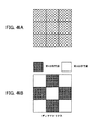
図4は、本実施形態のディザ処理部17においてディザマトリクスを用いてディザ処理を行う場合について説明するための図である。
このディザ法は、図4Aに示すように、複数画素で構成される中間階調で現される画像領域を、図4Bで示すように水平方向または垂直方向に碁盤目状の規則的な模様で表される第1の特性値(本実施形態においては透過率)の画素と、第2の特性値(本実施形態においては透過率)の画素の2つの画素で構成される2次元的なディザマトリクスにより擬似的に表現するものである。
ディザ処理部17は、このようなディザマトリクスで表現される出力信号Coutを表示部19に出力する。FIG. 4 is a diagram for explaining a case where dither processing is performed using a dither matrix in the
In this dither method, as shown in FIG. 4A, an image area represented by a halftone composed of a plurality of pixels is displayed in a regular grid pattern in the horizontal or vertical direction as shown in FIG. 4B. A two-dimensional dither composed of two pixels, a pixel having a first characteristic value (transmittance in the present embodiment) and a pixel having a second characteristic value (transmittance in the present embodiment). This is expressed in a pseudo manner by a matrix.
The
表示部19は、たとえば液晶を駆動するための薄膜トランジスタ(TFT)を搭載した直視型の液晶表示面を介してディザ処理部17の出力画像を表示する。
表示部19は、たとえば、電圧値として定義される出力信号Coutに対応した透過率曲線を有する液晶材料特性を利用して、所定の透過率(特性値)を得て中間階調表示を行う。The
The
次に、本発明の第1の実施形態に係る画像表示装置10より上述した2次元的なディザマトリクスを生成するまでの動作について説明をする。
Next, operations until the above-described two-dimensional dither matrix is generated from the
図5は、入力階調に対して補正すべき画素出力の関係を示す図である。
図5において、横軸が入力階調(透過率)を示し、縦軸が特性値(透過率)を示している。FIG. 5 is a diagram showing the relationship of the pixel output to be corrected with respect to the input gradation.
In FIG. 5, the horizontal axis indicates the input gradation (transmittance), and the vertical axis indicates the characteristic value (transmittance).
通常のディザ法においては、所定のディザ係数を対応する位置の複数の画素に加算し、複数の画素による加算された平均出力が、入力階調に対して図5中、直線bで示される線形関係となるように入力信号を補正して画素出力を得ることになる。
これに対して、本実施形態の画像表示装置10においては、入力階調に対して、例えば一対の画素(サブピクセル)をそれぞれ図5中、a、cで示される画素出力の関係に基づいてこれを補正し、第1の特性値VALaと、第2の特性値VALcを得るように制御する。
具体的には、この補正においては、図5に示すように直線bに対してプラスの補正値Δk2を加算して第1の特性値VALaを求めるとともに、直線bに対してマイナスの補正値Δk1を引算して第2の特性値VALcを求める。
換言すれば、入力階調に対して正の補正値としてのΔk2と負の補正値としてのΔk1を生成し、これらの補正値を入力階調に加算することで、画素出力bを得る。In a normal dither method, a predetermined dither coefficient is added to a plurality of pixels at corresponding positions, and an average output obtained by the plurality of pixels is linearly represented by a straight line b in FIG. The pixel output is obtained by correcting the input signal so as to satisfy the relationship.
On the other hand, in the
Specifically, in this correction, as shown in FIG. 5, a positive correction value Δk2 is added to the straight line b to obtain the first characteristic value VALa, and a negative correction value Δk1 to the straight line b. Is subtracted to obtain the second characteristic value VALc.
In other words, Δk2 as a positive correction value and Δk1 as a negative correction value with respect to the input gradation are generated, and these correction values are added to the input gradation to obtain the pixel output b.
ディザ処理部17には、入力階調に対してaの関係を持つ画素出力を示す信号V1と、入力階調に対してcの関係を持つ画素出力を示す信号V2が供給される。
ディザ処理部17においては、このような信号V1に基づき第1の特性値VALaを決定するとともに、信号V2に基づき第2の特性値VALcを決定し、ディザマトリクスを介して中間階調を表現する。
その結果、第1の特性値VALaと第2の特性値VALbをプラスして2で割った中間階調がディザマトリクスで表現されることになる。
これは、図5に示すa,cの関係で表される画素出力(透過率)を加算して2で割った関係がディザマトリクスを介して表現されることに相当する。
The
In the
As a result, ing in the intermediate tone divided by 2 the first characteristic value VALa and second characteristic values VALb plus is represented by the dither matrix.
This is equivalent to the fact that the pixel output (transmittance) represented by the relationship between a and c shown in FIG. 5 is added and divided by 2 is expressed via the dither matrix.
ちなみに、オフセット生成部12は、入力階調に対する画素出力a,cの関係を予めオフセットテーブルに記憶させておき、映像信号Hが入力される度にこのオフセットテーブルを参照して、補正値Δk1、Δk2を特定する。
オフセットテーブル中に予め記憶させておく画素出力の関係a,cは、図5に示すように、入力階調に対して正の補正値Δk2を加算した第1の特性値VALaに変換される画素と、負の補正値Δk1を加算した第2の特性値VALcに変換される画素を、それぞれディザマトリクス中に少なくとも1つずつ含む形式となるように設定される。
Incidentally, the offset
The pixel output relationships a and c stored in advance in the offset table are converted into a first characteristic value VALa obtained by adding a positive
たとえば、負の補正値Δk1と正の補正値Δk2を加算した結果得られる第1の特性値または第2の特性値の何れか一方が最大特性値(透過率100%)または最小特性値(透過率0%)となるように画素出力の関係a,cをオフセットテーブル中に記憶させる。
図5においては、透過率0%から50%に至るまで第2の特性値が最小特性値となるように負の補正値Δk1を設定しておくとともに、透過率50%から100%に至るまで第1の特性値が最大特性値となるように正の補正値Δk2を設定している。For example, either the first characteristic value or the second characteristic value obtained as a result of adding the negative correction value Δk1 and the positive correction value Δk2 is the maximum characteristic value (
In FIG. 5, the negative correction value Δk1 is set so that the second characteristic value becomes the minimum characteristic value from 0% to 50% transmittance, and from 50% to 100% transmittance. The positive correction value Δk2 is set so that the first characteristic value becomes the maximum characteristic value.
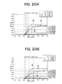
図6Aおよび図6Bは、上述したように補正値を設定した場合における表示部19の液晶表示面への各視野角(0度、20度、40度および60度)に対する透過率の関係を示す図であって、図6Aは通常のディザ法に基づく場合の視野角に対する透過率の関係を示し、図6Bは本実施形態における視野角に対する透過率の関係を示している。
図6Aおよび図6Bにおいて、横軸が表示部19において表示すべき階調に応じてディザ処理部17から供給された出力信号Coutに基づく透過率(入力)を示しており、縦軸は、実際に表示部19において表示される階調の透過率(出力)を示している。6A and 6B show the relationship of the transmittance with respect to each viewing angle (0 degree, 20 degrees, 40 degrees and 60 degrees) to the liquid crystal display surface of the
6A and 6B, the horizontal axis indicates the transmittance (input) based on the output signal Cout supplied from the
通常のディザ法に基づき、入力階調に対して図5中に直線bで示される線形関係に基づいてこれを補正して画素出力を得た場合には、図6Aに示すように、視野角が大きくなるにつれて、換言すれば液晶表示面を斜めから視認した場合において、視野角特性が著しく劣化することが分かる。 When the pixel output is obtained by correcting this based on the linear relationship indicated by the straight line b in FIG. 5 with respect to the input gradation based on the normal dither method, as shown in FIG. In other words, it can be seen that, in other words, when the liquid crystal display surface is viewed obliquely, the viewing angle characteristics are significantly deteriorated.
これに対して、本実施形態のように、画素出力の関係a,cとなるように第1の特性値、第2の特性値を決定した場合には、図6Bに示すように、液晶表示面を斜めから視認した場合においても、視野角特性が改善されていることが分かる。 On the other hand, when the first characteristic value and the second characteristic value are determined so as to have the pixel output relationship a, c as in the present embodiment, as shown in FIG. 6B, the liquid crystal display It can be seen that the viewing angle characteristics are improved even when the surface is viewed obliquely.
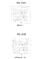
図7Aおよび図7Bは、図6Aおよび図6Bに示す透過率の関係をγ補正した階調で表した結果を示す図である。図7Aおよび図7Bにおいて、横軸が入力階調を、縦軸が出力階調をそれぞれ示している。 FIG. 7A and FIG. 7B are diagrams showing the results of expressing the relationship of transmittance shown in FIG. 6A and FIG. In FIG. 7A and FIG. 7B, the horizontal axis indicates the input gradation, and the vertical axis indicates the output gradation.
入力階調に対して実際に液晶表示面を介して人間の目で視認できる階調(以下、出力階調という。)は、通常のディザ法に基づき入力階調に対して図5中の直線bで示される線形関係に基づいてこれを補正して画素出力を得た場合には、図7Aに示すように、視野角が大きくなるにつれて入力階調と出力階調との線形性が徐々にズレていく。これは、液晶表示面を斜めから視認した場合において、視野角特性が著しく劣化することを示唆している。 A gradation (hereinafter referred to as an output gradation) that can be visually recognized by the human eye through the liquid crystal display surface with respect to the input gradation is a straight line in FIG. 5 with respect to the input gradation based on a normal dither method. When the pixel output is obtained by correcting this based on the linear relationship indicated by b, the linearity between the input gradation and the output gradation gradually increases as the viewing angle increases, as shown in FIG. 7A. It will shift. This suggests that the viewing angle characteristics are significantly deteriorated when the liquid crystal display surface is viewed obliquely.
これに対して、本実施形態にように、画素出力の関係a,cとなるように第1の特性値、第2の特性値を決定した場合には、図7Bに示すように、液晶表示面を斜めから視認した場合においても、視野角特性が改善されていることが分かる。 On the other hand, when the first characteristic value and the second characteristic value are determined so that the pixel output relations a and c are obtained as in the present embodiment, as shown in FIG. It can be seen that the viewing angle characteristics are improved even when the surface is viewed obliquely.
このように視野角が改善される理由としては、たとえば透過率が50%である場合には、図5に示すように、画素出力の関係a,cにおいて、第1の特性値は、透過率100%となるように、また第2の特性値は透過率0%となるようにディザマトリクスが構成されることになる。
透過率が0%、100%の場合には視野角特性は劣化することはないため、これに基づく第1の特性値と第2の特性値をプラスして2で割ることにより表現されるディザマトリクスの中間階調は、透過率50%においては、視野角特性は劣化することはない。
図6Bに示すように透過率50%においては、視野角に応じたズレが生じていないことが分かる。The reason why the viewing angle is improved as described above is that, for example, when the transmittance is 50%, as shown in FIG. 5, in the pixel output relationships a and c, the first characteristic value is the transmittance. The dither matrix is configured so that the second characteristic value is 0% and the transmittance is 0%.
Since the viewing angle characteristics do not deteriorate when the transmittance is 0% or 100%, the dither expressed by adding the first characteristic value and the second characteristic value based on this and dividing by 2 With regard to the halftone of the matrix, the viewing angle characteristic does not deteriorate at a transmittance of 50%.
As shown in FIG. 6B, it can be seen that there is no deviation according to the viewing angle at a transmittance of 50%.
また、透過率0%から透過率50%に至るまでにおいても、本実施形態においては、図5に示すように、第2の特性値を透過率0%で固定して、第1の特性値のみについて透過率を変えていくため、少なくとも第2の特性値に関しては視野角特性を劣化させることはなくなる。
このため、これら第1の特性値と第2の特性値をプラスして2で割ることにより表現されるディザマトリクスの中間階調を表示する場合に、通常のディザ法と比較して視野角特性を改善することができる。Further, in the present embodiment, as shown in FIG. 5, the second characteristic value is fixed at the transmittance of 0% and the first characteristic value is also obtained from the transmittance of 0% to the transmittance of 50%. Therefore, the viewing angle characteristic is not deteriorated at least with respect to the second characteristic value.
For this reason, when displaying an intermediate gray level of a dither matrix expressed by adding the first characteristic value and the second characteristic value and dividing by two, the viewing angle characteristic is compared with the normal dither method. Can be improved.
同様に、透過率50%から透過率100%に至るまでにおいても、本実施形態においては、図5に示すように、第1の特性値を透過率100%で固定して、第2の特性値のみについて透過率を変えていくため、少なくとも第1の特性値に関しては視野角特性を劣化させることはなくなる。
このため、これら第1の特性値と第2の特性値をプラスして2で割ることにより表現されるディザマトリクスの中間階調を表示する場合に、通常のディザ法と比較して視野角特性を改善することができる。Similarly, in the present embodiment from the transmittance of 50% to the transmittance of 100%, in the present embodiment, as shown in FIG. 5, the first characteristic value is fixed at the transmittance of 100% and the second characteristic is obtained. Since the transmittance is changed for only the value, the viewing angle characteristic is not deteriorated at least for the first characteristic value.
For this reason, when displaying an intermediate gray level of a dither matrix expressed by adding the first characteristic value and the second characteristic value and dividing by two, the viewing angle characteristic is compared with the normal dither method. Can be improved.
このように、本実施形態の画像表示装置10においては、第1の特性値と第2の特性値でディザマトリクスの中間階調を表現する場合に、いずれか一方の濃度を0%または100%に固定しているため、その分視野角特性を改善することが可能となる。
As described above, in the
なお、本実施形態においては、第1の特性値または第2の特性値の何れか一方が最大特性値または最小特性値となるような画素出力の関係a,cがオフセットテーブル中に記憶させている場合に限定されるものではない。
入力階調に対して正の補正値Δk2を加算した第1の特性値(透過率)に変換される画素と、負の補正値Δk1を加算した第2の特性値(透過率)に変換される画素を、それぞれディザマトリクス中に少なくとも1つずつ含む形とされていれば同様の効果を得ることができる。たとえば、図5に示す画素出力の関係がa’,c’で規定されるような曲線をオフセットテーブル中に記憶させていてもよい。
In this embodiment, pixel output relationships a and c such that either the first characteristic value or the second characteristic value is the maximum characteristic value or the minimum characteristic value are stored in the offset table. It is not limited to the case.
And a pixel to be converted to a positive correction value .
また、上述した実施の形態では、2つの画素でディザマトリクスを構成する場合について説明をしたが、本発明はこのような場合に限定されるものではなく、複数の画素でディザマトリクスが構成されていればいかなるものであってもよい。 In the above-described embodiment, the case where the dither matrix is configured by two pixels has been described. However, the present invention is not limited to such a case, and the dither matrix is configured by a plurality of pixels. Anything may be used.
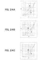
たとえば、図8Aに示すようなF1からF4の4つの画素で一つのディザマトリクスを構成する場合には、入力階調に対して補正すべき画素出力の関係は、図8Bに示すように、透過率0%から25%においては、画素F1の画素出力の特性値(透過率)を大きくシフトさせる一方、画素F2,F3,F4を最小特性値に固定する。
透過率25%から50%においては、画素F2の画素出力の特性値を大きくシフトさせる一方、画素F1の透過率を最大値(特性値)に固定し、さらに画素F3,F4の最小特性値に固定する。
透過率50%から75%においては、画素F3の画素出力の特性値を大きくシフトさせる一方、画素F1、F2を最大特性値に固定し、さらに画素F4を最小特性値に固定する。
透過率75%から100%においては、画素F4の画素出力の特性値を大きくシフトさせる一方、画素F1、F2、F3を最大特性値に固定する。For example, when one dither matrix is configured with four pixels F1 to F4 as shown in FIG. 8A, the relationship between the pixel output to be corrected with respect to the input gradation is transparent as shown in FIG. 8B. When the rate is 0% to 25%, the pixel output characteristic value (transmittance) of the pixel F1 is greatly shifted, while the pixels F2, F3, and F4 are fixed to the minimum characteristic value.
When the transmittance is 25% to 50%, the characteristic value of the pixel output of the pixel F2 is greatly shifted, while the transmittance of the pixel F1 is fixed to the maximum value (characteristic value) and further to the minimum characteristic value of the pixels F3 and F4. Fix it.
When the transmittance is from 50% to 75%, the pixel output characteristic value of the pixel F3 is greatly shifted, while the pixels F1 and F2 are fixed to the maximum characteristic value, and the pixel F4 is fixed to the minimum characteristic value.
When the transmittance is from 75% to 100%, the pixel output characteristic value of the pixel F4 is greatly shifted, while the pixels F1, F2, and F3 are fixed to the maximum characteristic value.
その結果、図8B中直線bに示すような画素出力を擬似的に作り出すことが可能となる。また、このような場合において、画素F1からF4のうち、少なくとも3つの画素は常に最小特性値(透過率0%)若しくは最大特性値(透過率100%)に固定されることになるため、視野角特性の劣化を防ぐことも可能となる。
As a result, it becomes possible to create a pseudo pixel output as shown by the straight line b in FIG. 8B. In such a case, at least three of the pixels F1 to F4 are always fixed to the minimum characteristic value (
このように、本第1の実施形態の画像表示装置10においては、第1の特性値と第2の特性値でディザマトリクスの中間階調を表現する場合に、このディザマトリクスを構成する1の画素の特性値のみをシフトさせ、他の画素の特性値は常に特性値(透過率)を0%または100%に固定しているため、その分視野角特性を改善することが可能となる。
As described above, in the
次に、入力された映像信号の中間階調を複数のフィールドで構成されるフィールド列で表現することにより視野角特性を改善した第2の実施形態に係る画像処理装置20について説明をする。
Next, a description will be given of an
第1の実施形態の画像表示装置10においては、空間方向へのディザ処理の手法を用いて、複数の画素により1つの階調を表現し、視野角特性を改善していた。
これに対して、第2の実施形態の画像表示装置20においては、時間方向に並ぶ複数の画面の画素により1つの階調を表現して、視野角特性を改善するものである。
以下、1枚の画面のことをフィールドとも呼び、複数のフィールドで構成される列をフィールド列と呼ぶものとする。なお、本明細書におけるフィールドと言う言葉は、いわゆる飛び越し走査におけるフィールドに限らない。In the
On the other hand, in the
Hereinafter, one screen is also called a field, and a column composed of a plurality of fields is called a field column. Note that the term field in this specification is not limited to a field in so-called interlaced scanning.
図9は、第2の実施形態に係る画像表示装置20の構成例を示すブロック図である。
FIG. 9 is a block diagram illustrating a configuration example of the
画像表示装置20は、図9に示すように、非線形変換部21と、オフセット生成部22と、オフセットテーブル23と、第1の加算回路24と、第2の加算回路25と、第1の逆変換部26と、第2の逆変換部27と、時分割処理部28と、時分割処理部28を制御する制御部29と、表示部30とを備えている。
As shown in FIG. 9, the
非線形変換部21には、たとえば画面表示レートが60Hzの映像信号Hが、外部から入力される。
非線形変換部21は、入力された映像信号Hを、予め設定されている所定の非線形の入出力特性に従って、レベル変換をする。
非線形変換部21に設定される非線形の入出力特性は、たとえば低レベルになるにつれて勾配が緩やかになるいわゆるガンマ関数で表される非線形曲線である。ただし、この非線形の入出力特性は、任意に設定可能である。For example, a video signal H having a screen display rate of 60 Hz is input to the
The
The non-linear input / output characteristic set in the
非線形変換部21から出力されたレベル変換後の映像信号Lは、第1の加算回路24および第2の加算回路25に供給される。
The level-converted video signal L output from the
オフセット生成部22は、映像信号Hが入力される。オフセット生成部22は、オフセットテーブル23を参照して、第1のオフセット信号Δk1および第2のオフセット信号Δk2を発生する。
オフセットテーブル23は、入力された映像信号Hの信号レベルに対する対応するオフセット信号Δk1およびΔk2の値が示されたテーブルである。
オフセット生成部22は、入力された映像信号Hに応じて対応するΔk1およびΔk2をオフセットテーブルから検索して、オフセット信号として出力する。
なお、オフセット生成部22から出力される第1のオフセット信号Δk1および第2のオフセット信号Δk2についての詳細は後述する。The offset
The offset table 23 is a table in which values of offset signals Δk1 and Δk2 corresponding to the signal level of the input video signal H are shown.
The offset
Details of the first offset signal Δk1 and the second offset signal Δk2 output from the offset
オフセット生成部22から出力された第1のオフセット信号Δk1は、第1の加算回路24に供給される。オフセット生成部22から出力された第2のオフセット信号Δk2は、第2の加算回路25に供給される。
The first offset signal Δk1 output from the offset
第1の加算回路24には、非線形変換部21から出力された映像信号Lと、オフセット生成部22から出力された第1のオフセット信号Δk1とが入力される。
第1の加算回路24は、映像信号Lと第1のオフセット信号Δk1とを加算した映像信号E1を生成する。
第1の加算回路24により生成された映像信号E1は、第1の逆変換部26に供給される。The
The
The video signal E1 generated by the
第2の加算回路25には、非線形変換部21から出力された映像信号Lと、オフセット生成部22から出力された第2のオフセット信号Δk2とが入力される。
第2の加算回路25は、映像信号Lから、第1のオフセット信号Δk1を減算した映像信号E2を生成する。
第2の加算回路24により生成された映像信号E2は、第2の逆変換部27に供給される。The video signal L output from the
The
The video signal E2 generated by the
第1の逆変換部26には、第1の加算回路24から出力された映像信号E1が入力される。第1の逆変換部26は、入力された映像信号E1を、予め設定されている所定の非線形の入出力特性に従って、レベル変換をする。
The video signal E <b> 1 output from the
第2の逆変換部27には、第2の加算回路25から出力された映像信号E2が入力される。第2の逆変換部27は、入力された映像信号E2を、予め設定されている所定の非線形の入出力特性に従って、レベル変換をする。
The video signal E <b> 2 output from the
第1の逆変換部26および第2の逆変換部27に設定されている非線形の入出力特性は、非線形変換部21に設定されている非線形の入出力特性の逆特性である。
たとえば、非線形変換部21にガンマ関数に応じた入出力特性が設定されていれば、第1の逆変換部26および第2の逆変換部27には逆ガンマ特性が設定されていることとなる。
このため、非線形変換部21に設定されている非線形特性を更新した場合には、これに連動させて第1の逆変換部26および第2の逆変換部27に設定されている非線形特性をも更新することになる。The nonlinear input / output characteristics set in the first
For example, if input / output characteristics corresponding to the gamma function are set in the
For this reason, when the nonlinear characteristic set in the
第1の逆変換部26によりレベル変換がされた後の映像信号V1は、時分割処理部28に供給される。また、第2の逆変換部27によりレベル変換がされた後の映像信号V2も、時分割処理部28に供給される。
The video signal V <b> 1 after level conversion by the first
なお、非線形変換部21は、第1の実施形態の画像表示装置10の輝度変換部11と同一の構成要素を有し、オフセット生成部22およびオフセットテーブル23は、第1の実施形態の画像表示装置10のオフセット生成部12と同一の構成要素を有し、第1の加算回路24は、第1の実施形態の画像表示装置10の第1の加算回路13と同一の構成要素を有し、第2の加算回路25は、第1の実施形態の画像表示装置10の第2の加算回路14と同一の構成要素を有する。さらに、第1の逆変換部26は、第1の実施形態の画像表示装置10の第1の電圧変換部15と同一の構成要素を有し、第2の逆変換部27は、第1の実施形態の画像表示装置10の第2の電圧変換部26と同一の構成要素を有する。
The
さらに、以上の各構成要素の接続関係も第1の実施形態の画像表示装置10と同様である。
Further, the connection relationship of the above constituent elements is the same as that of the
時分割処理部28は、第1のアップコンバート部281と、第2のアップコンバート部282と、切換出力部283とを有している。
The time
第1のアップコンバート部281には、第1の逆変換部26によりレベル変換がされた後の映像信号V1が入力される。映像信号V1は、元々の映像信号Hと同様の画面表示レート(60Hz)である。
第1のアップコンバート部281は、入力された映像信号V1の画面表示レートを、60Hzから120Hzに、アップコンバートする。第1のアップコンバート部281は、たとえば同じ画面を2回繰り返し出力することによりアップコンバートを行う。The first up-
The first up-
第2のアップコンバート部282には、第2の逆変換部27によりレベル変換がされた後の映像信号V2が入力される。映像信号V2は、元々の映像信号Hと同様の画面表示レート(60Hz)である。
第2のアップコンバート部282は、入力された映像信号V2の画面表示レートを、60Hzから120Hzに、アップコンバートする。第2のアップコンバート部282は、たとえば同じ画面を2回繰り返し出力することによりアップコンバートを行う。The second up-
The second up-
切換出力部283は、第1のアップコンバート部281から出力された映像信号と、第2のアップコンバート部281から出力された映像信号とを、1画面毎に交互に選択して出力する。
The switching
このため、切換出力部283からは、第1のオフセット信号Δk1が加算されて生成された画面と、第2のオフセット信号Δk2が加算されて生成された画面とが、1画面毎に交互に繰り返された画面表示レートが120Hzの映像信号Coutが出力される。
切換出力部283から出力された映像信号Coutは、表示部40に供給される。For this reason, from the switching
The video signal Cout output from the switching
表示部30は、たとえば液晶を駆動する薄膜トランジスタ(TFT)を搭載した直視型の液晶表示面を介して時分割処理部28の出力画像を表示する。
表示部30では、液晶表示面が、映像信号Coutに対応して各画素位置において透過率が変化し、映像信号の各画面を表示する。ここで、画面表示レートは120Hzであっても、液晶の交流化は60Hzにする。液晶に直流が印加され、焼きつきやフリッカを生じることをふせぐためである。The
In the
次に、第2の実施形態に係る画像表示装置20の処理動作について説明する。
Next, the processing operation of the
画像表示装置20においては、時間方向に並ぶ連続した2つの画面により1つの階調を表現して、視野角特性を改善する。具体的には、次のような処理を行っている。
In the
画像表示装置20においては、映像信号の画面表示レートを60Hzから120Hzにアップコンバートする。
ここで、画面表示レートをアップコンバートした後の映像信号の連続した2枚の画面のうち、先行する画面のことを「第1フィールド」、後の画面のことを「第2フィールド」と呼ぶものとする。
なお、フィールドと呼んでいるが、飛び越し走査のフィールドとは関係がない。In the
Here, of the two consecutive screens of the video signal after the screen display rate is up-converted, the preceding screen is called “first field”, and the subsequent screen is called “second field”. And
Although called a field, it has nothing to do with the interlaced scanning field.
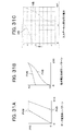
図10は、入力された映像信号Hの信号レベル(階調)に対する、表示部30に表示される特性値(液晶の透過率)を示す図である。
FIG. 10 is a diagram showing characteristic values (liquid crystal transmittance) displayed on the
画像表示装置20においては、図10に示すように、第1フィールドFLD1に対しては第1のオフセット信号Δk1を加算し、第2のフィールドFLD2に対しては、第2のオフセット信号Δk2を減算するようにしている。
In the
このため、画像表示装置20においては、プラス側にレベルが補正されたフィールド(第1フィールド)と、マイナス側にレベルが補正されたフィールドとが交互に繰り返される出力映像信号Coutが表示部30に供給される。
For this reason, in the
ここで、人間の目の視覚の特性は、時間方向に対する積分特性があるため、プラス側に補正されたフィールドとマイナス側に補正されたフィールドとが交互に表示された場合には、その平均値のレベルの画像であると認識する。
そのため、表示部30に表示された映像を見たユーザは、第1フィールドFLD1と第2のフィールドFLD2との平均のレベルで表された映像信号AFDL12を擬似的に見ていることとなる。
したがって、画像表示装置20においては、第1フィールドFLD1と第2フィールドFLD2とを平均化したときに、オフセット信号Δk1,Δk2を加算しなかった場合の通常の映像を見たのと同じ映像となるように、オフセット信号Δk1,Δk2を定めている。Here, since the visual characteristics of the human eye have an integral characteristic with respect to the time direction, if the field corrected on the plus side and the field corrected on the minus side are displayed alternately, the average value thereof is displayed. It is recognized as an image of the level.
Therefore, the user who has viewed the video displayed on the
Therefore, in the
画像表示装置20のオフセット生成部22は、第1のオフセット信号Δk1および第2のオフセット信号Δk2をオフセットテーブル23を参照して発生する。
オフセットテーブル23は、元の映像信号のレベル(入力階調)に対する画素出力レベルの関係を予め記憶している。オフセット生成部22は、映像信号Hが入力される度にオフセットテーブル23を参照して、Δk1、Δk2を特定する。The offset
The offset table 23 stores in advance the relationship between the pixel output level and the level (input gradation) of the original video signal. The offset
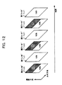
たとえば、図11に示すような、画面上半分の領域が50%の透過率の階調で表示される領域であり、画面下半分の領域が100%の透過率の階調で表示される領域の画面wを表示する場合を考える。 For example, as shown in FIG. 11, the upper half area of the screen is an area displayed with a gradation of 50% transmittance, and the lower half area of the screen is an area displayed with a gradation of 100% transmittance. Consider the case where the screen w is displayed.
この場合、図12に示すように、第1フィールドFDL1は、全面が100%の透過率の階調で表示される画像となる。また、第2のフィールドFLD2は、画面上半分の領域が0%の透過率の階調で表示され、画面下半分の領域が100%の透過率の階調で表示される。
画面wを表示する場合、このような第1フィールドFLD1および第2フィールドFLD2が交互に表示されるため、上半分の領域の濃度が、擬似的に0%と100%との合成の濃度として視認される画像を表示することができる。In this case, as shown in FIG. 12, the first field FDL1 is an image displayed on the entire surface with a gradation of 100% transmittance. In the second field FLD2, the upper half area of the screen is displayed with a gradation of 0% transmittance, and the lower half area of the screen is displayed with a gradation of 100% transmittance.
When the screen w is displayed, since the first field FLD1 and the second field FLD2 are alternately displayed, the density of the upper half region is visually recognized as a synthetic density of 0% and 100%. The displayed image can be displayed.
また、画像表示装置20においては、第1のオフセット信号Δk1を加算した結果値と、第2のオフセット信号Δk2を減算した結果値との何れか一方が、最大特性値(透過率100%)または最小特性値(透過率0%)となるように、オフセットテーブル23中にΔk1およびΔk2が記憶させている。
前記の図10においては、入力された映像信号のレベルが0%から50%に至るまでは第2フィールドFLD2の特性値(透過率)が最小値(最小透過率)となるように第2のオフセット信号Δk2が設定してあるとともに、入力された映像信号のレベルが50%から100%に至るまでは第1フィールドFLD1の特性値(透過率)が最大値(最大透過率)となるように第1のオフセット信号Δk1を設定してある。Further, in the
In FIG. 10, the second field FLD2 has a minimum value (minimum transmittance) so that the characteristic value (transmittance) of the second field FLD2 becomes the minimum value (minimum transmittance) until the level of the input video signal reaches 0% to 50%. The offset signal Δk2 is set, and the characteristic value (transmittance) of the first field FLD1 becomes the maximum value (maximum transmittance) until the level of the input video signal reaches 50% to 100%. A first offset signal Δk1 is set.
このため、たとえば、中間階調e1を表現する場合には、図13Aに示すように、時刻t0から時刻t1/2に至るまでの第1フィールドFLD1を透過率g1に基づくものとし、時刻t1/2から時刻t1に至るまでの第2フィールドFLD2を透過率0%とする。
これにより、時刻t0から時刻t1に至るまでの連続したフィールドの並び(以下、フィールド列という。)を視認したユーザに対して、その画像領域について中間階調e1を擬似的に映し出すことが可能となる。Therefore, for example, when expressing the intermediate gradation e1, as shown in FIG. 13A, the first field FLD1 from time t0 to time t1 / 2 is based on the transmittance g1, and the time t1 / The second field FLD2 from 2 to time t1 is assumed to have a transmittance of 0%.
As a result, it is possible for a user who has viewed a continuous field sequence (hereinafter referred to as a field sequence) from time t0 to time t1 to simulate the intermediate gradation e1 for the image area. Become.
また、たとえば、中間階調e2を表現する場合には、図13Bに示すように、時刻t0から時刻t1/2に至るまでの第1フィールドFLD1を透過率g2に基づくものとし、時刻t1/2から時刻t1に至るまでの第2フィールドFLD2を透過率0%とする。
これにより、時刻t0から時刻t1に至るまでのフィールド列を連続して視認したユーザに対して、その画像領域について中間階調e2を擬似的に映し出すことが可能となる。Further, for example, when expressing the intermediate gradation e2, as shown in FIG. 13B, the first field FLD1 from time t0 to time t1 / 2 is based on the transmittance g2, and the time t1 / 2. The second field FLD2 from time t1 to time t1 is set to 0% transmittance.
As a result, it becomes possible for the user who has continuously viewed the field sequence from time t0 to time t1 to display the intermediate gradation e2 in a pseudo manner for the image region.
さらに、たとえば、透過率の高い中間階調e3を表現する場合には、図13Cに示すように、時刻t0から時刻t1/2に至るまでの第1フィールドFLD1を透過率100%に基づくものとし、時刻t1/2から時刻t1に至るまで第2のフィールドFLD2を透過率g3とする。
これにより、時刻t0から時刻t1に至るまでのフィールド列を連続して視認したユーザに対して、その画像領域について中間階調e3を擬似的に映し出すことが可能となる。Further, for example, when expressing an intermediate gray level e3 having a high transmittance, as shown in FIG. 13C, the first field FLD1 from time t0 to time t1 / 2 is based on the transmittance of 100%. From the time t1 / 2 to the time t1, the second field FLD2 is set to the transmittance g3.
As a result, it becomes possible for the user who has continuously viewed the field sequence from time t0 to time t1 to project the intermediate gradation e3 in a pseudo manner for the image region.
このように、本発明を適用した画像表示装置20においては、第1の特性値(透過率)と第2の特性値(透過率)でディザマトリクスの中間階調を表現する場合に、いずれか一方の特性値を最小特性値(透過率0%)または最大特性値(透過率100%)に固定している。
この特性値(透過率)0%並びに100%はともに視野角特性が良好であるため、いずれか一方の特性値を最小特性値、最大特性値に設定することで、その分視野角特性を改善することが可能となる。As described above, in the
Both of these characteristic values (transmittance) 0% and 100% have good viewing angle characteristics. Therefore, setting one of the characteristic values to the minimum characteristic value and the maximum characteristic value improves the viewing angle characteristics accordingly. It becomes possible to do.
このようなオフセット信号Δk1,Δk2を設定した場合における表示部30の液晶表示面への各視野角に対する透過率の関係は、空間ディザの場合と同様に改善がされる。
When such offset signals Δk1 and Δk2 are set, the relationship of the transmittance with respect to each viewing angle on the liquid crystal display surface of the
なお、第2の実施形態においては、2つの連続したフィールドにより1つの階調を表示してるいが、本発明はこれに限らず、2以上の連続したフィールドから構成されるフィールド列内に、映像信号の階調に対して正の補正値(オフセット値)を加算した特性値に変換されるフィールドと、映像信号の階調に対して負の補正値(オフセット値)を加算した特性値に変換されるフィールドを、少なくとも1つずつ含むようにして階調表現を行えば、どのようにしてもよい。 In the second embodiment, one gradation is displayed by two continuous fields. However, the present invention is not limited to this, and the field sequence composed of two or more continuous fields includes: A field converted to a characteristic value obtained by adding a positive correction value (offset value) to the gradation of the video signal, and a characteristic value obtained by adding a negative correction value (offset value) to the gradation of the video signal Any method may be used as long as gradation expression is performed so as to include at least one field to be converted.
なお、本発明は、上述した第1の実施形態および第2の実施形態に限定されるものではなく、たとえば入力された映像信号Hが動画像で構成されている場合には、ディザ処理部17において、2次元画像としてのディザマトリクスを用いて中間階調を表現するように制御し、また入力された映像信号Hが静止画像で構成されている場合には、フィールド列を用いて中間階調を表現するように制御してもよい。
The present invention is not limited to the first embodiment and the second embodiment described above. For example, when the input video signal H is composed of a moving image, the
また、本実施形態に係る画像表示装置においては、中間階調をディザマトリクスで表現する構成とフィールド列で表現する構成の何れも備えるようにしてもよいし、何れか一方のみ備えるようにしてもよい。 In addition, the image display apparatus according to the present embodiment may be provided with either a configuration in which the intermediate gradation is expressed by a dither matrix or a configuration in which the gray scale is expressed by a field column, or only one of them. Good.
また、この画像表示装置においては、白黒画像の中間階調を表現する場合に限定されるものではなく、RGBの原色輝度成分で表される映像信号の中間階調を同様の手法に基づいて表現するようにしてもよい。 This image display device is not limited to the representation of the intermediate gradation of a black and white image, but represents the intermediate gradation of a video signal represented by RGB primary color luminance components based on a similar method. You may make it do.
また、この画像表示装置10においては、オフセット生成部12において設定する補正値としてのΔk1、Δk2をユーザが事前において任意に設定できるようにしてもよいことは勿論である。
In the
また、この画像表示装置10においては、液晶表示面を斜めから視認した場合におけるいわゆる斜め視野角を測定し、測定した斜め視野角に基づいてディザ処理部17におけるディザ処理を最適化するようにしてもよい。
Further, in the
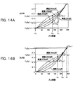
一般に斜め視野角において黒浮きが生じないのは、視野角補償フィルムを配置することによる効果が大きく、また中間階調においては、ガンマ特性のズレが大きくなるところ、RGBが異なる階調としての記憶色の肌色の色抜け現象として目立つことになる。これらを解決するためには、ガンマ特性の斜め視野角の変化を少なくする必要がある。 In general, black floating does not occur at an oblique viewing angle because the effect of arranging a viewing angle compensation film is great, and in the intermediate gradation, the gamma characteristic shift becomes large. This will be prominent as the color loss phenomenon of skin color. In order to solve these problems, it is necessary to reduce the change in the oblique viewing angle of the gamma characteristic.
このため、平均化すると元のレベルが同じ輝度(透過率)になる互いにΔT離れた2値を求める。 For this reason, two values that are separated from each other by ΔT are obtained to obtain the same luminance (transmittance) when the average level is obtained.
図14Aおよび図14Bは視野角が0度、30度、45度及び60度の場合における入力階調に対する透過率特性を示している。たとえば図14Aで示すようにT1(v1)と、T2(v2)を平均化した結果得られる輝度をT0(v0)とする。また、実測したガンマ特性が図14Aに示すように暗い方向へシフトしていた場合には、
T60_org=T0(v0)+ΔT(v0)・・・・・・・・・・・・・・・(1)
T60_dither=
(T0(v1)+ΔT(v1)+T0(v2)+ΔT(v2))/2
=T0(v1)/2+ΔT(v1)/2+T0(v2)/2+ΔT(v2)/2
・・・・・・・・・・・・・(2)
T0(v0)=(T1(v1)+T2(v2))/2・・・・・・・・・(3)
であることから、
T60_dither=T0(v0)+ΔT(v1)/2+T0(v2)/2・・・・(4)
となる。
ただし上述の変数は以下の値を示す。
v0:目的とする中間調を表示するための通常駆動電圧、
v1:本発明での正の補正値を加算した特性値を得るための駆動電圧、
v2:本発明での負の補正値を減算した特性値を得るための駆動電圧、
T0(v0):目的とする中間調透過率、
T1(v1):本発明での正の補正値を加算した特性値、
T2(v2):本発明での負の補正値を減算した特性値、
ΔT(v0):v0での視角60°透過率と視角0°透過率との差、
ΔT(v1):v1での視角60°透過率と視角0°透過率との差、
ΔT(v2):v2での視角60°透過率と視角0°透過率との差、
T60_org:通常駆動での視角60°透過率、
T60_dither:本発明での視角60°透過率。14A and 14B show the transmittance characteristics with respect to the input gradation when the viewing angles are 0 degree, 30 degrees, 45 degrees, and 60 degrees. For example, as shown in FIG. 14A, the luminance obtained as an average of T1 (v1) and T2 (v2) is T0 (v0). In addition, when the actually measured gamma characteristic is shifted in the dark direction as shown in FIG. 14A,
T60_org = T0 (v0) + ΔT (v0) (1)
T60_dither =
(T0 (v1) + ΔT (v1) + T0 (v2) + ΔT (v2)) / 2
= T0 (v1) / 2 + ΔT (v1) / 2 + T0 (v2) / 2 + ΔT (v2) / 2
(2)
T0 (v0) = (T1 (v1) + T2 (v2)) / 2 (3)
Because
T60_dither = T0 (v0) + ΔT (v1) / 2 + T0 (v2) / 2 (4)
It becomes.
However, the above variables show the following values.
v0: normal driving voltage for displaying the target halftone,
v1: Drive voltage for obtaining a characteristic value obtained by adding a positive correction value in the present invention;
v2: driving voltage for obtaining a characteristic value obtained by subtracting the negative correction value in the present invention;
T0 (v0): target halftone transmittance,
T1 (v1): a characteristic value obtained by adding a positive correction value in the present invention,
T2 (v2): a characteristic value obtained by subtracting the negative correction value in the present invention,
ΔT (v0): difference between the
ΔT (v1): difference between the
ΔT (v2): difference between the
T60_org: viewing
T60_dither: viewing
また、ΔT(v1)/2+ΔT(v2)/2<ΔT(v0)であることから、ΔT60_dither<ΔT60_orgとなり、視野角による輝度変動は少なくなる。このような場合におけるΔTは片側が0にクリップされるまで、互いに離れた条件が最も改善され、ガンマ特性の斜め視野角の変化が少なくなる。 Further, since ΔT (v1) / 2 + ΔT (v2) / 2 <ΔT (v0), ΔT60_dither <ΔT60_org, and the luminance variation due to the viewing angle is reduced. In such a case, until ΔT is clipped to 0, ΔT is most improved in the condition of being separated from each other, and the change in the oblique viewing angle of the gamma characteristic is reduced.
また、実測したガンマ特性が図14Bに示すように明るい方向へシフトしていた場合には、ΔT(v1)/2+ΔT(v2)/2>ΔT(v0)であるから、ΔT60_dither>ΔT60_orgとなり、視野角による輝度変動は悪化する。この場合には、元の値T(V0)を使うか、ΔTを変えて最適点を探すことになる。 Further, when the actually measured gamma characteristic is shifted in the bright direction as shown in FIG. 14B, ΔT (v1) / 2 + ΔT (v2) / 2> ΔT (v0), so ΔT60_dither> ΔT60_org, and the field of view Luminance fluctuation due to corners gets worse. In this case, the original value T (V0) is used or ΔT is changed to search for the optimum point.
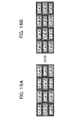
次に、求めた2値を利用して空間ディザをかける。このとき、各画素について上述の如くガンマ特性に応じて2値を求め、求めた2値のうち元の画素の明るさより明るい点T(v1)と暗い点T(v2)を図15Aに示すように千鳥配置状に表示する。
ちなみに、RGBに関しても同様に千鳥配置状に表示する場合には、(r1,g1,b1)からなる輝度と、(r2,g2,b2)からなる輝度の2値で表されることになる。Next, spatial dither is applied using the obtained binary values. At this time, binary values are obtained for each pixel according to the gamma characteristic as described above, and a point T (v1) and a dark point T (v2) that are brighter than the brightness of the original pixel are shown in FIG. 15A. Are displayed in a staggered arrangement.
Incidentally, when RGB is displayed in a staggered arrangement, it is represented by a binary value of luminance consisting of (r1, g1, b1) and luminance consisting of (r2, g2, b2).
このようにして空間ディザをかけた後に、さらに時間ディザをかける。図15Bは、図15Aにおいて求められた千鳥配置状のパターンを時間の経過に応じて逆転させて交互に表示させる例を示している。
このように空間ディザと時間ディザを重ね合わせることにより、フリッカもなく網目も目立たない視野角の広がった良質の合成画像を作り出すことが可能となる。After applying spatial dither in this way, further time dither is applied. FIG. 15B shows an example in which the staggered pattern obtained in FIG. 15A is reversed and displayed alternately over time.
By superimposing the spatial dither and the temporal dither in this way, it is possible to create a high-quality composite image with a wide viewing angle that is free from flicker and is not conspicuous.
なお、RGBに関して上述の如き千鳥配置状に表示する場合において、何れか一の原色輝度成分を入れ替えるようにしてもよい。 In the case of displaying the RGB in the staggered arrangement as described above, any one primary color luminance component may be replaced.
図16Aおよび図16Bは、RGBのうち、Gのみを入れ替える例を示している。この図16A、Bに示す例では、(r1,g2,b1)からなる輝度と、(r2,g1,b2)からなる輝度の2値で千鳥配置状に空間配置するとともに、時間ディザをかけることによりこれらの配置を逆転させる。
このような場合には、白黒の千鳥配置ではなくGの補色市松配置の如き印象をユーザに与えることになる。
すなわち、この図16A,Bの例では、隣り合う画素の輝度差が少なく、網目も見えにくく、エッジもよりスムーズに見えることになり、また各画素についてディザ値を求めているため解像度の劣化が少ない。16A and 16B show an example in which only G of RGB is replaced. In the example shown in FIGS. 16A and 16B, spatial arrangement is made in a zigzag arrangement with two values of luminance consisting of (r1, g2, b1) and luminance (r2, g1, b2), and time dithering is applied. To reverse these arrangements.
In such a case, an impression such as a G complementary checkered arrangement of G is given to the user instead of a black and white staggered arrangement.
That is, in the example of FIGS. 16A and 16B, the luminance difference between adjacent pixels is small, the mesh is difficult to see, the edges look smoother, and since the dither value is obtained for each pixel, the resolution is degraded. Few.
図17は、測定した斜め視野角に基づいてディザ処理を最適化する構成を上記画像表示装置10に組み込む例を示している。
FIG. 17 shows an example in which a configuration for optimizing the dither processing based on the measured oblique viewing angle is incorporated in the
図15Aに示すように千鳥配置状に表示する。(r1,g1,b1)からなる輝度と、(r2,g2,b2)からなる輝度の2値でディザマトリクスを構成する場合には、入力された輝度(r0,g0,b0)からなる映像信号Hが入力される2値生成部31と、この2値生成部31に接続された斜め視野角パラメータ部32と、ディザ処理部17Aとで構成されることになる。
As shown in FIG. 15A, the images are displayed in a staggered arrangement. When a dither matrix is composed of two values of luminance consisting of (r1, g1, b1) and luminance (r2, g2, b2), a video signal consisting of input luminance (r0, g0, b0) A
2値生成部31は、入力された映像信号Hに対して上記式(1)〜式(4)に基づき、輝度(r1,g1,b1)と、輝度(r2,g2,b2)を求める。この2値生成部31において求められた2値の輝度は、それぞれディザ処理部17Aへと送信される。
The
ちなみに2値生成部31は、これら2値の輝度を求める際において、測定した斜め視野角がパラメータ化されて管理されている斜め視野角パラメータ部32を参照することになる。
Incidentally, the
ディザ処理部17Aは、これら輝度(r1,g1,b1)と、輝度(r2,g2,b2)が2値生成部31へ送られてきた場合には、これに基づいて上述の如きディザ処理を実行することになる。
When the luminance (r1, g1, b1) and the luminance (r2, g2, b2) are sent to the
上述したように、第2の実施形態として、時間方向に並ぶ連続した2つの画面により1つの階調を表現して、視野角特性を改善する時間的なディザ法を説明した。
以下に、本第2の実施形態の概念に含まれる入力された映像信号の中間階調を複数のフィールドで構成されるフィールド列で表現する場合であって、以下に示す駆動方法について説明する。As described above, as the second embodiment, the temporal dither method for improving the viewing angle characteristic by expressing one gradation by two continuous screens arranged in the time direction has been described.
In the following, a driving method described below, which is a case where the intermediate gray level of the input video signal included in the concept of the second embodiment is expressed by a field sequence composed of a plurality of fields, will be described.
以下においては、液晶に印加する駆動電圧の黒レベルの電圧選定を最適化、パネル厚を最適化して、液晶応答波形を、いわゆるパルス幅変調(PWM)の波形に近づけて視野角特性を改善する第1の方法、白レベルの電圧選定を最適化およびパネル厚を最適化して視野角特性を改善する第2の方法、並びに、明と暗の時間比率を変えてパネルを駆動して視野角特性を改善する第3の方法について、順を追って説明する。 In the following, the selection of the black level of the driving voltage applied to the liquid crystal is optimized, the panel thickness is optimized, and the liquid crystal response waveform is brought closer to the so-called pulse width modulation (PWM) waveform to improve the viewing angle characteristics. A first method, a second method for optimizing white level voltage selection and a panel thickness to improve the viewing angle characteristics, and driving the panel by changing the time ratio of light and dark to view angle characteristics A third method for improving the above will be described step by step.
まず、液晶に印加する駆動電圧の黒レベルの電圧選定を最適化して、図18に示すように、液晶応答波形を、いわゆるパルス幅変調(PWM)の波形に近づけて視野角特性を改善する第1の方法について説明する。
First, the black level voltage selection of the drive voltage applied to the liquid crystal is optimized, and the liquid crystal response waveform is made closer to a so-called pulse width modulation (PWM) waveform as shown in FIG. The
一般的な液晶ディスプレイ装置においては、駆動電圧を、たとえば図19AのXで示す範囲、すなわち、黒レベルはしきい値電圧、たとえば1.9Vと略同様の値に設定され、白レベルは4.0Vに設定される。
この場合の、駆動電圧波形を図19Bに、入力階調に対する透過率特性を図19Cに示している。
この場合、実効的駆動電圧波形の立ち上がり、立ち上がり部分が十分な急峻さを得られておらず(十分な応答特性が得られておらず)、視野角60度におけるγ特性は、Bで示す実際の特性もAで示す理想曲線と異なる波形が得られる傾向にある。In a general liquid crystal display device, the driving voltage is set to a range indicated by X in FIG. 19A, for example, the black level is set to a threshold voltage, for example, approximately the same value as 1.9 V, and the white level is set to 4. Set to 0V.
The drive voltage waveform in this case is shown in FIG. 19B, and the transmittance characteristics with respect to the input gradation are shown in FIG. 19C.
In this case, the rising and rising portions of the effective drive voltage waveform are not sufficiently steep (sufficient response characteristics are not obtained), and the γ characteristic at a viewing angle of 60 degrees is actually indicated by B. There is also a tendency that a waveform different from the ideal curve indicated by A is obtained.
これに対して、本実施形態に係る第1の方法においては、駆動電圧を、図19AのYで示す範囲、すなわち、黒レベルはしきい値電圧、たとえば1.9Vより低い電圧、図19Aの例では0Vに設定され、白レベルは4.0Vに設定される。
この場合の、駆動電圧波形を図19Dに、入力階調に対する透過率特性を図19Eに示している。
この場合、実効的な駆動電圧波形の立ち上がり、立ち上がり部分が十分な急峻さを得られており(十分な応答特性が得られており)、パルス幅を実効的に狭くするように制御できており、視野角60度におけるγ特性は、Bで示す実際の特性もAで示す理想曲線に近似した波形が得られる傾向にある。
すなわち、黒レベルの電圧値を、しきい値より低い値(この値は低いほど(0Vに近づくほど)良好な応答特性を得られる駆動電圧波形を形成することが可能である。)に設定することにより、図18に示すように、液晶応答波形を、いわゆるパルス幅変調(PWM)の波形に近づけて中間階調の視野角特性を改善することが可能となる利点がある。
また、液晶応答特性が改善されることから、動画に対する応答も改善される利点がある。On the other hand, in the first method according to the present embodiment, the drive voltage is set in a range indicated by Y in FIG. 19A, that is, the black level is a threshold voltage, for example, a voltage lower than 1.9V, In the example, it is set to 0V, and the white level is set to 4.0V.
The drive voltage waveform in this case is shown in FIG. 19D, and the transmittance characteristics with respect to the input gradation are shown in FIG. 19E.
In this case, the rise and rise of the effective drive voltage waveform are sufficiently steep (sufficient response characteristics are obtained), and can be controlled to effectively narrow the pulse width. The γ characteristic at a viewing angle of 60 degrees tends to obtain a waveform in which the actual characteristic indicated by B approximates the ideal curve indicated by A.
That is, the voltage value of the black level is set to a value lower than the threshold value (the lower this value is (the closer to 0V), the more it is possible to form a drive voltage waveform that can obtain a good response characteristic). As a result, as shown in FIG. 18, there is an advantage that the liquid crystal response waveform can be brought close to a so-called pulse width modulation (PWM) waveform to improve the viewing angle characteristics of the intermediate gradation.
Further, since the liquid crystal response characteristics are improved, there is an advantage that the response to the moving image is also improved.
次に、白レベルの電圧選定を最適化および液晶材料の屈折率異方性Δnと液晶層の厚みdの積で表される光学的なセル厚Δndを最適化して視野角特性を改善する第2の方法について説明する。
Next, the white-level voltage selection is optimized and the optical cell thickness Δnd expressed by the product of the refractive index anisotropy Δn of the liquid crystal material and the thickness d of the liquid crystal layer is optimized to improve the viewing angle characteristics. The
本第2の方法においては、基本的には、白レベルの電圧を最大の透過率を示す4Vではなく、4Vより大きい値、たとえば5Vに設定する。
図20Aに示すように、R,G,B信号を個別に観察すると、R,Gは白レベルで駆動電圧として4Vを印加しても、透過率を最大レベルに保持可能であるが、B信号は透過率が低くなっていく傾向にある。
そこで、本実施形態においては、図20Bに示すように、白レベルの電圧を最大の透過率を示す4Vではなく、4Vより大きい値、たとえば5Vに設定している。白レベルとして5Vを設定することにより、白表示時の透過率を4V時のレベルあるいはそれ以上に保持させることが可能となる。
そして、本実施形態の第2の方法においては、画素セルの光学的なセル厚Δndを通常の液晶ディスプレイ装置においては、波長546nm(Gの波長近傍)に対して310nmであったものを270nmに設定し、波長450nm(Bの波長近傍)に対して330nmであったものを285nmに設定している。
すなわち、本第2の方法を採用する液晶パネルには、光学的なセル厚を薄くなるように構成している。
なお、本第2の方法において、黒レベルは通常の液晶ディスプレイ装置と同様にしきい値の近傍値、あるいは、第1の方法と同様に、しきい値より低く設定する。In the second method, basically, the white level voltage is set to a value larger than 4V, for example, 5V, instead of 4V indicating the maximum transmittance.
As shown in FIG. 20A, when the R, G, and B signals are individually observed, the transmittance can be maintained at the maximum level even when 4V is applied as a drive voltage at the white level for R and G. Tends to decrease the transmittance.
Therefore, in the present embodiment, as shown in FIG. 20B, the white level voltage is set to a value larger than 4V, for example, 5V, instead of 4V indicating the maximum transmittance. By setting 5V as the white level, it is possible to maintain the transmittance at the time of white display at the level of 4V or higher.
In the second method of this embodiment, the optical cell thickness Δnd of the pixel cell is changed from 310 nm to 270 nm with respect to the wavelength of 546 nm (near the wavelength of G) in a normal liquid crystal display device. The wavelength was set to 285 nm, which was 330 nm with respect to the wavelength 450 nm (near the wavelength of B).
In other words, the liquid crystal panel employing the second method is configured so that the optical cell thickness is reduced.
In the second method, the black level is set to a value near the threshold value as in a normal liquid crystal display device, or lower than the threshold value as in the first method.
図21Aに図20Aに相当する一般的な液晶ディスプレイ装置の入力階調に対する透過率特性を、図21Bに図20Bに相当する本実施形態の第2の方法を採用する液晶ディスプレイ装置の入力階調に対する透過率特性を示す。 FIG. 21A shows the transmittance characteristics with respect to the input gradation of a general liquid crystal display device corresponding to FIG. 20A, and FIG. 21B shows the input gradation of the liquid crystal display device employing the second method of this embodiment corresponding to FIG. 20B. The transmittance characteristics with respect to are shown.
一般的な液晶ディスプレイ装置は、図21Aに示すように、視野角60度におけるγ特性は、Bで示す実際の特性もAで示す理想曲線と異なる波形が得られる傾向にある。
これに対して、本実施形態に係る第2の方法においては、視野角60度におけるγ特性は、Bで示す実際の特性もAで示す理想曲線に近似した波形が得られる傾向にある。
すなわち、液晶の駆動電圧の白レベルの値を透過率が略最大となり始める4Vではなく、4Vより高い電圧、たとえば5Vに設定し、これに対応して画素セルの光学的厚さを所定波長に対して薄くなるように構成することにより、中間階調の視野角特性を改善することが可能となる利点がある。In a general liquid crystal display device, as shown in FIG. 21A, the γ characteristic at a viewing angle of 60 degrees tends to obtain a waveform having an actual characteristic indicated by B different from the ideal curve indicated by A.
On the other hand, in the second method according to the present embodiment, the γ characteristic at the viewing angle of 60 degrees tends to obtain a waveform in which the actual characteristic indicated by B also approximates the ideal curve indicated by A.
That is, the value of the white level of the driving voltage of the liquid crystal is set to a voltage higher than 4 V, for example 5 V, instead of 4 V at which the transmittance starts to become substantially maximum, and the optical thickness of the pixel cell is set to a predetermined wavelength correspondingly On the other hand, it is advantageous to be able to improve the viewing angle characteristics of the intermediate gradation by making it thinner.
なお、本実施形態においては、白レベルの駆動電圧(印加電圧)を一般的なディスプレイ装置に比べて25%高くし、光学的セル厚を86%程度に薄く設定しているが、本発明は、この割合に限定されるものではく、種々の態様が可能である。また、さらに液晶材料として、粘度の低いものを使用することにより、液晶の応答速度が速くなり、上述の第2の実施形態に適用することで視野角特性を改善することができる。 In this embodiment, the white level driving voltage (applied voltage) is set to 25% higher than that of a general display device, and the optical cell thickness is set to be as thin as 86%. However, the present invention is not limited to this ratio, and various modes are possible. Further, by using a liquid crystal material having a low viscosity, the response speed of the liquid crystal is increased, and the viewing angle characteristics can be improved by applying to the second embodiment described above.
次に、明と暗の時間比率を変えてパネルを駆動して視野角特性を改善する第3の方法について説明する。 Next, a third method for improving viewing angle characteristics by driving the panel while changing the time ratio between light and dark will be described.
本第3の方法は、基本的に、明と暗の時間的な比率を1:2となるように駆動方法を採用する。
この場合、たとえば図22に示すように垂直方向(V)のラインを線順次ではなく、明暗を交互にアクセスするが、暗データが明データの2倍となるようなアクセス方法を採用する。The third method basically employs a driving method so that the temporal ratio of light to dark is 1: 2.
In this case, for example, as shown in FIG. 22, the lines in the vertical direction (V) are accessed alternately instead of line-sequentially, but the access method is adopted in which the dark data is twice as bright as the bright data.
たとえば、Vライン数が768である場合に、明と暗の時間的な比率を1:2となるように駆動する場合、以下のような駆動制御を行う。なお、以下の説明ではライン数は#符号に数字を付して示す。 For example, when the number of V lines is 768 and driving is performed so that the temporal ratio of light to dark is 1: 2, the following drive control is performed. In the following description, the number of lines is indicated by adding a number to the # sign.
まず、ライン#1を明データとしてアクセス、次にライン#513を暗データとしてアクセスし、次にライン#2を明データとしてアクセスし、次にライン#514を暗データとしてアクセスし、以後、これを順番に繰り返し、ライン#256を明データとしてアクセスし、次に、ライン#768(最終ライン)を暗データとしてアクセスし、次にライン#257を明データとしてアクセスする。
一通り上述の順でアクセスし、次いで、今度は、ライン#1を暗データとしてアクセスし、次二ライン#258を明データとしてアクセスし、次にライン#2を暗データとしてアクセスし、以後これを順番に繰り返す。
以上の駆動方法により、明と暗との時間比率を1:1ではなく、1:2として液晶パネルを駆動することが可能である。First,
Access in the order described above, then access
With the above driving method, it is possible to drive the liquid crystal panel by setting the time ratio of light and dark to 1: 2 instead of 1: 1.
図23Aに一般的な液晶ディスプレイ装置の入力階調に対する透過率特性を、図23Bに本実施形態の第3の方法を採用する液晶ディスプレイ装置の入力階調に対する透過率特性を示す。 FIG. 23A shows transmittance characteristics with respect to input gradations of a general liquid crystal display device, and FIG. 23B shows transmittance characteristics with respect to input gradations of a liquid crystal display device employing the third method of the present embodiment.
一般的な液晶ディスプレイ装置は、図23Aに示すように、視野角60度におけるγ特性は、Bで示す実際の特性もAで示す理想曲線と異なる波形が得られる傾向にある。
これに対して、本実施形態に係る第3の方法においては、視野角60度におけるγ特性は、Bで示す実際の特性もAで示す理想曲線に近似した(近づいた)波形が得られる傾向にある。
すなわち、明と暗の時間的な比率を1:2となるように駆動することにより、中間階調の視野角特性を改善することが可能となる利点がある。そしてこの比率は1:2に限定されるものではなく、明と暗の時間的な比率を変えて、特に明と暗の比率のうち暗の比率が大きくなるように駆動することにより、中間階調の視野角特性を改善することが可能となる。As shown in FIG. 23A, a general liquid crystal display device has a tendency that a gamma characteristic at a viewing angle of 60 degrees has a waveform different from an ideal curve indicated by A in terms of an actual characteristic indicated by B.
On the other hand, in the third method according to the present embodiment, the γ characteristic at the viewing angle of 60 degrees tends to obtain a waveform that approximates (approaches) the actual characteristic indicated by B to the ideal curve indicated by A. It is in.
That is, there is an advantage that it is possible to improve the viewing angle characteristics of the intermediate gradation by driving the light to dark temporal ratio to be 1: 2. This ratio is not limited to 1: 2, but by changing the temporal ratio of light and dark, and by driving to increase the dark ratio among the ratios of light and dark, It is possible to improve the viewing angle characteristics of the tone.
以上、明と暗の時間的な比率を1:2となるように駆動する好適な液晶パネルの駆動方法として、第1〜第3の方法を例に説明した。
これらの方法は、組み合わせて採用することも可能である。たとえば第2の方法(白レベルを5Vに設定し、光学的セル厚を薄くする方法。)と第3の方法(明と暗の時間的な比率を変える方法)を組み合わせた第4の方法、あるいは、いわゆる空間サブピクセル(たとえば面積比2:1)と第2の方法とを組み合わせた第5の方法を採用することも可能である。As described above, the first to third methods have been described as examples of the preferred liquid crystal panel driving method for driving the light to dark time ratio to be 1: 2.
These methods can also be employed in combination. For example, a fourth method combining the second method (a method in which the white level is set to 5 V and the optical cell thickness is reduced) and the third method (a method in which the temporal ratio of light and dark is changed); Alternatively, a fifth method combining a so-called spatial subpixel (for example, an area ratio of 2: 1) and the second method may be employed.
図24Aに一般的な液晶ディスプレイ装置の入力階調に対する透過率特性を、図24Bに本実施形態の第2の方法を採用する液晶ディスプレイ装置の入力階調に対する透過率特性を、図24Cに第2の方法と第3の方法を組み合わせた第4の方法を採用した液晶ディプレイ装置の入力階調に対する透過率特性を示す。
FIG. 24A shows the transmittance characteristics with respect to the input gradation of a general liquid crystal display device, FIG. 24B shows the transmittance characteristics with respect to the input gradation of the liquid crystal display device employing the second method of this embodiment, and FIG. The transmittance characteristic with respect to the input gradation of the liquid crystal display device adopting the fourth method combining the
前述しているように、一般的な液晶ディスプレイ装置は、図24Aに示すように、視野角60度におけるγ特性は、Bで示す実際の特性もAで示す理想曲線と異なる波形が得られる傾向にある。
これに対して、本実施形態に係る第2の方法においては、図24Bに示すように、視野角60度におけるγ特性は、Bで示す実際の特性もAで示す理想曲線に近似した波形が得られる傾向にある。
さらに、本実施形態の第4の方法においては、図24Cに示すように、第2の方法に比較して、視野角60度におけるγ特性は、Bで示す実際の特性もAで示す理想曲線にさらに近似した波形が得られる傾向にある。
したがって、第4の方法を採用しても中間階調の視野角特性を改善することが可能である利点がある。As described above, in a general liquid crystal display device, as shown in FIG. 24A, the γ characteristic at a viewing angle of 60 degrees tends to obtain a waveform different from the ideal curve indicated by A in the actual characteristic indicated by B. It is in.
On the other hand, in the second method according to the present embodiment, as shown in FIG. 24B, the γ characteristic at a viewing angle of 60 degrees has a waveform that approximates the ideal characteristic indicated by A as well as the actual characteristic indicated by B. It tends to be obtained.
Furthermore, in the fourth method of the present embodiment, as shown in FIG. 24C, compared to the second method, the γ characteristic at a viewing angle of 60 degrees is an ideal curve in which the actual characteristic indicated by B is also indicated by A. There is a tendency to obtain a waveform that more closely approximates to.
Therefore, even if the fourth method is adopted, there is an advantage that the viewing angle characteristics of the intermediate gradation can be improved.
図25Aに一般的な空間サブピクセル処理に対応した液晶ディスプレイ装置の入力階調に対する透過率特性を、図25Bに本実施形態の第2の方法と空間サブピクセル処理を組み合わせた第5の方法を採用した液晶ディプレイ装置の入力階調に対する透過率特性を示す。 FIG. 25A shows the transmittance characteristics with respect to the input gradation of the liquid crystal display device corresponding to general spatial subpixel processing, and FIG. 25B shows the fifth method combining the second method of this embodiment and the spatial subpixel processing. The transmittance characteristic with respect to the input gradation of the adopted liquid crystal display device is shown.
前述しているように、一般的な液晶ディスプレイ装置は、図25Aに示すように、視野角60度におけるγ特性は、Bで示す実際の特性もAで示す理想曲線と異なる波形が得られる傾向にある。
これに対して、本実施形態に係る第5の方法においては、図24Bに示すように、視野角60度におけるγ特性は、Bで示す実際の特性もAで示す理想曲線に近似した良好な特性波形が得られる傾向にある。
したがって、第5の方法を採用しても中間階調の視野角特性を改善することが可能である利点がある。As described above, in a general liquid crystal display device, as shown in FIG. 25A, the γ characteristic at a viewing angle of 60 degrees tends to obtain a waveform having an actual characteristic indicated by B different from the ideal curve indicated by A. It is in.
On the other hand, in the fifth method according to the present embodiment, as shown in FIG. 24B, the γ characteristic at the viewing angle of 60 degrees is good in that the actual characteristic indicated by B also approximates the ideal curve indicated by A. A characteristic waveform tends to be obtained.
Therefore, even if the fifth method is adopted, there is an advantage that the viewing angle characteristics of the intermediate gradation can be improved.
次に、明と暗時の液晶セルの駆動電圧について説明する。 Next, the driving voltage of the liquid crystal cell during light and dark will be described.
図26Aに一般的な液晶ディスプレイ装置の入力に対する明と暗時の液晶セルに印加する電圧特性波形を、図26Bに本実施形態の第2の方法を採用する液晶ディスプレイ装置の入力に対する明と暗時の液晶セルに印加する電圧特性波形を、図26Cに第2の方法と第3の方法を組み合わせた第4の方法を採用した液晶ディプレイ装置の入力に対する明と暗時の液晶セルに印加する電圧特性波形を示す。
各図において、VWで示す曲線が明時の液晶セルへの印加電圧波形を示し、VBで示す曲線が暗時の液晶セルへの印加電圧波形を示している。
図に示すように、本実施形態の方法を採用した液晶ディスプレイ装置は、黒レベルの表現範囲が広くなり、実効的に中間階調の視野角特性を改善することが可能である。FIG. 26A shows voltage characteristic waveforms applied to the liquid crystal cell during light and dark with respect to the input of a general liquid crystal display device, and FIG. 26B shows light and dark with respect to the input of the liquid crystal display device employing the second method of this embodiment. The voltage characteristic waveform applied to the liquid crystal cell at the time is applied to the liquid crystal cell at the time of light and dark with respect to the input of the liquid crystal display device adopting the fourth method combining the second method and the third method in FIG. A voltage characteristic waveform is shown.
In each figure, the curve indicated by VW indicates the voltage waveform applied to the liquid crystal cell during light and the curve indicated by VB indicates the voltage waveform applied to the liquid crystal cell during darkness.
As shown in the figure, the liquid crystal display device adopting the method of this embodiment has a wide black level expression range, and can effectively improve the viewing angle characteristics of the intermediate gradation.
図27Aに一般的な空間サブピクセル処理に対応した液晶ディスプレイ装置の入力に対する明と暗時の液晶セルに印加する電圧特性波形を、図27Bに本実施形態の第2の方法と空間サブピクセル処理を組み合わせた第5の方法を採用した液晶ディスプレイ装置の入力に対する明と暗時の液晶セルに印加する電圧特性波形を示す。
各図において、VWで示す曲線が明時の液晶セルへの印加電圧波形を示し、VBで示す曲線が暗時の液晶セルへの印加電圧波形を示している。
図に示すように、本実施形態の方法を採用した液晶ディスプレイ装置は、黒レベルの表現範囲が広くなり、実効的に中間階調の視野角特性を改善することが可能である。FIG. 27A shows voltage characteristic waveforms applied to the light and dark liquid crystal cells in response to the input of the liquid crystal display device corresponding to general spatial subpixel processing. FIG. 27B shows the second method and spatial subpixel processing of this embodiment. FIG. 6 shows voltage characteristic waveforms applied to a liquid crystal cell during light and dark with respect to an input of a liquid crystal display device adopting a fifth method combining the above.
In each figure, the curve indicated by VW indicates the voltage waveform applied to the liquid crystal cell during light and the curve indicated by VB indicates the voltage waveform applied to the liquid crystal cell during darkness.
As shown in the figure, the liquid crystal display device adopting the method of this embodiment has a wide black level expression range, and can effectively improve the viewing angle characteristics of the intermediate gradation.
本実施形態の第1〜第5の方法を採用する液晶ディスプレイ装置においては、図26A〜図26Cや図27A,Bに示す明の印加電圧VWと暗の印加電圧VBをフィールドごとに切り替えて液晶パネル前段のいわゆるソースドライバに供給する。 In the liquid crystal display device employing the first to fifth methods of the present embodiment, the liquid crystal display device is switched by switching the bright application voltage VW and the dark application voltage VB shown in FIGS. 26A to 26C and FIGS. 27A and 27B for each field. Supply to the so-called source driver in front of the panel.
以下に、これの方法に対応した液晶ディスプレイ装置の構成例について説明する。 Hereinafter, a configuration example of a liquid crystal display device corresponding to this method will be described.
図28は、本実施形態の駆動方法に適用可能な液晶ディスプレイ装置(画像表示装置)の第1の構成例を示す図である。 FIG. 28 is a diagram illustrating a first configuration example of a liquid crystal display device (image display device) applicable to the driving method of the present embodiment.
この液晶ディスプレイ装置40は、データ変換部41、基準電圧生成部42、ソースドライバ43、および表示部としての表示パネル部44を有する。データ変換部41、基準電圧生成部42、ソースドライバ43により駆動部が構成される。以下に示すディスプレイ装置の構成例において、入力信号は、画像表示レートが60Hzの通常の信号であっても、120Hzに画像表示レートを上げ補間した信号、若しくは、さらにオーバードライブ処理を行った信号であっても、本実施形態の駆動方法を適用することができる。
The liquid
データ変換部41は、γ切替部410を有し、γ切替部410は、第1フィールドγ特性保持部411、第2フィールドγ特性保持部412、およびγ切替スイッチ413を有している。
第1フィールドγ特性保持部411は、たとえば上述したγ特性に対応して設定された明電圧VWの特性電圧γパターンを、たとえばルックアップテーブル等の形態で保持する。
第2フィールドγ特性保持部412は、たとえば上述したγ特性に対応して設定された暗電圧VBの特性電圧γパターンを、たとえばルックアップテーブル等の形態で保持する。
γ切替スイッチ413は、第1フィールドγ特性保持部411と第2フィールドγ特性保持部412の出力データをフィールドごとに切り替えてソースドライバ信号としてソースドライバ43に選択的に出力する。
基準電圧生成部42は、固定の基準電圧パターンをソースドライバ43に供給する。
ソースドライバ43は、γ切替部410により選択的に供給されるソースドライバ信号を基準電圧パターンと比較して所定の駆動信号を表示パネル部44に出力する。The
The first field γ
The second field γ
The
The reference
The
この装置40に対して前述した駆動方法が採用されて、階調性能が改善される。
The driving method described above is adopted for the
図29は、本実施形態の駆動方法に適用可能な液晶ディスプレイ装置の第2の構成例を示す図である。 FIG. 29 is a diagram illustrating a second configuration example of the liquid crystal display device applicable to the driving method of the present embodiment.
この液晶ディスプレイ装置40Aは、基準電圧生成部42A、ソースドライバ43、および表示パネル部44を有する。
The liquid
図29の装置40Aが、図28の装置と異なる点は、γ切替部の機能を基準電圧生成部42Aに持たせ、元データは、ソースドライバ43に入力される。
The
基準電圧生成部42Aは、第1フィールドγ特性保持部421、第2フィールドγ特性保持部422、およびγ切替スイッチ423を有している。
第1フィールドγ特性保持部421は、たとえば上述したγ特性に対応して設定された明時の特性電圧γパターンを、たとえばルックアップテーブル等の形態で保持する。
第2フィールドγ特性保持部422は、たとえば上述したγ特性に対応して設定された暗時の特性電圧γパターンを、たとえばルックアップテーブル等の形態で保持する。
γ切替スイッチ423は、第1フィールドγ特性保持部421と第2フィールドγ特性保持部422の出力データをフィールドごとに切り替えて基準電圧としてソースドライバ43に選択的に出力する。
ソースドライバ43は、供給されるソースドライバ信号を基準電圧パターンと比較して所定の駆動信号を表示パネル部44に出力する。The reference
The first field γ
The second field γ
The
The
この装置40Aに対して前述した駆動方法が採用されて、階調性能が改善される。
The driving method described above is adopted for this
図30は、本実施形態の駆動方法に適用可能な液晶ディスプレイ装置の第3の構成例を示す図である。 FIG. 30 is a diagram illustrating a third configuration example of the liquid crystal display device applicable to the driving method of the present embodiment.
この液晶ディスプレイ装置40Bは、図28のγ切替部41と図29の切替機能を有する基準電圧生成部42Aを合わせ持つ構成を有する。
したがって、各部の基本的な機能についての説明は省略する。The liquid
Therefore, the description of the basic functions of each part is omitted.
図31Aにγ切替部410の第1フィールドγ特性保持部411、第2フィールドγ特性保持部412に保持されるデータ変換γパターンPVW,PVBを示し、図31Bに基準電圧生成部42Aの第1フィールドγ特性保持部421、第2フィールドγ特性保持部422に保持されるデータ変換γパターンPVW,PVBを示し、図31Cに入力データに対するソースドライバ43の出力(液晶印加電圧)特性を示す。
FIG. 31A shows the data conversion γ patterns PVW and PVB held in the first field γ
図30の装置40Bにおいては、ソースドライバ43において、γ切替部410からフィールドごとに選択的に供給されるγパターンと基準電圧生成部42Aからフィールドごとに選択的に供給されるγパターンとが比較されて、図31Cに示すような、明電圧VW、暗電圧VBが生成されて、表示パネル部44に供給される。
In the
この装置40Bに対して前述した駆動方法が採用されて、階調性能が改善される。
The driving method described above is adopted for this
図32は、本実施形態の駆動方法に適用可能な液晶ディスプレイ装置の第4の構成例を示す図である。 FIG. 32 is a diagram illustrating a fourth configuration example of the liquid crystal display device applicable to the driving method of the present embodiment.
この液晶ディスプレイ装置40Cが図30の装置40Bと異なる点は、RGBの各γ補正を行う用に構成したことにあり、基本的なデータ変換部41Cのγ切替部410Cの機能は同様である。また、基準電圧生成部42Aは、図30の装置40Bと同様の構成を有する。
したがって、各部の基本的な機能についての説明は省略する。The liquid crystal display device 40C is different from the
Therefore, the description of the basic functions of each part is omitted.
図33Aにγ切替部410Cの第1フィールドγ特性保持部411C、第2フィールドγ特性保持部412Cに保持されるRGB対応のデータ変換γパターンPVW,PVBを示し、図33Bに基準電圧生成部42Aの第1フィールドγ特性保持部421、第2フィールドγ特性保持部422に保持されるデータ変換γパターンPVW,PVBを示し、図33Cに入力データに対するRGB対応のソースドライバ43の出力(液晶印加電圧)特性を示す。
FIG. 33A shows RGB data conversion γ patterns PVW and PVB held in the first field γ characteristic holding unit 411C and the second field γ characteristic holding unit 412C of the γ switching unit 410C, and FIG. 33B shows the reference
図32の装置40Cにおいては、ソースドライバ43において、データ変換部41Cのγ切替部410Cからフィールドごとに選択的に供給されるRGB対応のγパターンと基準電圧生成部42Aからフィールドごとに選択的に供給されるγパターンとが比較されて、図31Cに示すような、明電圧VW、暗電圧VBが生成されて、表示パネル部44に供給される。
In the device 40C of FIG. 32 , in the
この装置40Cに対して前述した駆動方法が採用されて、階調性能が改善される。 The driving method described above is adopted for this device 40C, and the gradation performance is improved.
図34は、本実施形態の駆動方法に適用可能な液晶ディスプレイ装置の第5の構成例を示す図である。 FIG. 34 is a diagram illustrating a fifth configuration example of the liquid crystal display device applicable to the driving method of the present embodiment.
この液晶ディスプレイ装置40Dが図30の装置40Bと異なる点は、サブピクセル変調処理に対応した構成、すなわち、入力信号に対しサブピクセル1系とサブピクセル2系が並列に配置されていることにある。
各部の機能は図30と同様であることから、各部の基本的な機能についての説明は省略する。The liquid crystal display device 40D is different from the
Since the function of each part is the same as that of FIG. 30, description of the basic function of each part is omitted.
図35Aにγ切替部410−1の第1フィールドγ特性保持部411、第2フィールドγ特性保持部412に保持されるデータ変換γパターンPVW1,PVB1を示し、図35Bにγ切替部410−2の第1フィールドγ特性保持部411、第2フィールドγ特性保持部412に保持されるデータ変換γパターンPVW2,PVB2を示し、図35Cに基準電圧生成部42A−1の第1フィールドγ特性保持部421、第2フィールドγ特性保持部422に保持されるデータ変換γパターンPVW1,PVB1を示し、図35Dに基準電圧生成部42A−1の第1フィールドγ特性保持部421、第2フィールドγ特性保持部422に保持されるデータ変換γパターンPVW2,PVB2を示し、図35Eに入力データに対するソースドライバ43の出力(液晶印加電圧)特性を示す。
FIG. 35A shows the data conversion γ patterns PVW1 and PVB1 held in the first field γ
この装置40Dに対して前述した駆動方法が採用されて、階調性能が改善される。 The driving method described above is adopted for this device 40D, and the gradation performance is improved.
図36は、本実施形態の駆動方法に適用可能な液晶ディスプレイ装置の第6の構成例を示す図である。 FIG. 36 is a diagram illustrating a sixth configuration example of the liquid crystal display device applicable to the driving method of the present embodiment.
この液晶ディスプレイ装置40Eが図34の装置40Dと異なる点は、RGBの各γ補正を行う用に構成したことにあり、その他の構成は、装置40Dと同様である。
したがって、各部の基本的な機能についての説明は省略する。The liquid
Therefore, the description of the basic functions of each part is omitted.
図37Aにγ切替部410−1の第1フィールドγ特性保持部411、第2フィールドγ特性保持部412に保持されるRGB対応のデータ変換γパターンPVW1,PVB1を示し、図37Bにγ切替部410−2の第1フィールドγ特性保持部411、第2フィールドγ特性保持部412に保持されるRGB対応のデータ変換γパターンPVW2,PVB2を示し、図37Cに基準電圧生成部42A−1の第1フィールドγ特性保持部421、第2フィールドγ特性保持部422に保持されるデータ変換γパターンPVW1,PVB1を示し、図37Dに基準電圧生成部42A−1の第1フィールドγ特性保持部421、第2フィールドγ特性保持部422に保持されるデータ変換γパターンPVW2,PVB2を示し、図37Eおよび図37Fに入力データに対するソースドライバ43のRGB対応の出力(液晶印加電圧)特性を示す。
FIG. 37A shows RGB data conversion γ patterns PVW1 and PVB1 held in the first field γ
この装置40Eに対して前述した駆動方法が採用されて、階調性能が改善される。
The driving method described above is adopted for this
図38は、本実施形態の駆動方法に適用可能な液晶ディスプレイ装置の第7の構成例を示す図である。 FIG. 38 is a diagram illustrating a seventh configuration example of the liquid crystal display device applicable to the driving method of the present embodiment.
この液晶ディスプレイ装置40Fが図34の装置40Dと異なる点は、データ変換部41Eにおいてγ切替部410Eをサブピクセル1の第1および第2フィールドγ保持部とサブピクセル2野の第1および第2フィールドγ保持部を並列的に配置して、一つのγ切替スイッチ413Fで選択的に切り替えて出力し、RGBγ補正部414で補正した後、ソースドライバ43に出力するようにしたことにある。
したがって、図38の装置40Fは、ソースドライバ43、基準電圧生成部42Aを一つずつ設けるだけでサブピクセル変調処理に対応することができる。The liquid
Therefore, the
この装置40Eに対して前述した駆動方法が採用されて、階調性能が改善される。
The driving method described above is adopted for this
本画像表示装置および画像表示方法は、複数の画素を使用して中間階調を表示すると同時に視野角特性を改善可能なことから直視型の液晶表示装置等に適用可能である。
The image display device and the image display method can be applied to a direct-viewing type liquid crystal display device and the like because the viewing angle characteristics can be improved at the same time as displaying a halftone using a plurality of pixels.
Claims (9)
入力された映像信号の階調を表示すべき画像に対して二次元配列する各画素の特性値に階調変換する階調変換部と、
入力された映像信号の中間階調を当該映像信号より高い表示レートの2つのフィールドで構成されるフィールド列で表現する階調表現部と、
上記階調変換部および上記階調表現部を制御して入力された映像信号に基づき上記階調表示を行う制御部と、を有し、
上記階調変換部は、中間階調を表現する複数の画素のうち、入力された映像信号の階調に対して正の補正値を加算した第1の特性値に変換される画素、並びに負の補正値を加算した第2の特性値に変換される画素を、少なくとも1つずつ含むように上記階調変換を行い、
上記階調表現部は、入力された映像信号の階調に対して正の補正値を加算した第3の特性値に変換されるフィールド、並びに負の補正値を加算した第4の特性値に変換されるフィールドを、少なくとも1つずつ含むように上記階調表現を行い、
上記制御部は、
入力された映像信号が動画像を含む場合には、上記階調変換部を駆動して、中間階調を表現する複数の画素のうち、入力された映像信号の階調に対して正の補正値を加算した第1の特性値に変換される画素、並びに負の補正値を加算した第2の特性値に変換される画素を、少なくとも1つずつ含むように上記階調変換を行うように制御し、
入力された映像信号が静止画像で構成されている場合には、上記階調表現部を駆動して、入力された映像信号の階調に対して正の補正値を加算した第3の特性値に変換されるフィールド、並びに負の補正値を加算した第4の特性値に変換されるフィールドを、少なくとも1つずつ含むように上記階調表現を行うように制御する
画像表示装置。An image display device having a display unit capable of gradation display according to an input video signal,
A gradation converter that converts the gradation of the input video signal into a characteristic value of each pixel that is two-dimensionally arranged with respect to an image to be displayed;
A gradation expression unit that expresses an intermediate gradation of an input video signal by a field sequence composed of two fields having a higher display rate than the video signal;
And a control unit for performing the gradation display based on the tone conversion section and a video signal input by controlling the gradation portion,
The gradation conversion unit includes a pixel that is converted into a first characteristic value obtained by adding a positive correction value to a gradation of an input video signal among a plurality of pixels that express an intermediate gradation, and a negative value. The gradation conversion is performed so as to include at least one pixel to be converted into the second characteristic value obtained by adding the correction value of
The gradation expression unit converts the field to be converted into a third characteristic value obtained by adding a positive correction value to the gradation of the input video signal, and the fourth characteristic value obtained by adding a negative correction value. The gradation representation is performed so as to include at least one field to be converted,
The control unit
When the input video signal includes a moving image, the gradation conversion unit is driven to positively correct the gradation of the input video signal among a plurality of pixels expressing the intermediate gradation. The gradation conversion is performed so as to include at least one pixel converted to the first characteristic value added with the value and one pixel converted to the second characteristic value added with the negative correction value. Control
When the input video signal is composed of a still image, a third characteristic value obtained by driving the gradation expression unit and adding a positive correction value to the gradation of the input video signal And an image display device that controls the gradation expression so as to include at least one field to be converted into a fourth characteristic value obtained by adding a negative correction value .
上記表示部は、上記階調変換部により階調変換された上記第1および第2の特性値に対応して上記基準電圧生成部により生成された各フィールドの基準電圧により駆動される
請求項1記載の画像表示装置。A reference voltage generator for generating a reference voltage corresponding to the third characteristic value and the fourth characteristic value in the gradation expression unit;
The display unit according to claim 1 which is driven by the reference voltage of the field generated by the reference voltage generator in response to the gradation converted the first and second characteristic value by the tone converting section serial mounting image display device.
請求項1または2に記載の画像表示装置。The gradation conversion unit performs the gradation conversion so that one of the first characteristic value and the second characteristic value is a maximum characteristic value or a minimum characteristic value. Image display device.
上記階調表現部は、入力された映像信号の中間階調を当該映像信号より高い表示レートの2つのフィールドで構成されるフィールド列の実効的電圧で表現し、
上記表示部は、駆動電圧に応じた階調で表示する液晶画素セルを含み、
上記第1の電圧の最大値は、液晶セルの特性値が略最大となり始める電圧より高い電圧に設定されている
請求項1から3のいずれか一に記載の画像表示装置。Includes a driver for generating a first voltage and a second driving dynamic voltage that corresponds to the voltage corresponding to the dark level is darker than the input video signal corresponding to a brighter light level from the input video signal,
The gradation expression unit expresses an intermediate gradation of an input video signal with an effective voltage of a field sequence composed of two fields having a higher display rate than the video signal,
The display unit includes a liquid crystal pixel cell that displays at a gradation corresponding to a driving voltage,
4. The image display device according to claim 1, wherein the maximum value of the first voltage is set to a voltage higher than a voltage at which the characteristic value of the liquid crystal cell starts to become substantially maximum. 5.
上記階調表現部は、入力された映像信号の中間階調を当該映像信号より高い表示レートの2つのフィールドで構成されるフィールド列の実効的電圧で表現し、
上記表示部は、駆動電圧に応じた階調で表示する液晶画素セルを含み、入力された映像信号より明るい明レベルと入力された映像信号より暗い暗レベルとで表示される時間的な比率を変えて駆動される
請求項1から4のいずれか一に記載の画像表示装置。A drive unit for generating the drive voltage corresponding to a first voltage corresponding to a brighter light level than the input video signal and a second voltage corresponding to a darker level darker than the input video signal;
The gradation expression unit expresses an intermediate gradation of an input video signal with an effective voltage of a field sequence composed of two fields having a higher display rate than the video signal,
The display unit includes a liquid crystal pixel cell that displays at a gradation corresponding to a driving voltage, and displays a temporal ratio of displaying a bright level brighter than the input video signal and a dark level darker than the input video signal. The image display device according to claim 1, wherein the image display device is driven by being changed.
請求項5記載の画像表示装置。The image display device according to claim 5, wherein the display unit is driven such that a temporal ratio displayed at a dark level out of a temporal ratio between the bright level and the dark level is increased.
入力された映像信号の階調を表示すべき画像に対して二次元配列する各画素の特性値に階調変換する階調変換ステップと、
入力された映像信号の中間階調を当該映像信号より高い表示レートの2つのフィールドで構成されるフィールド列で表現する階調表現ステップと、
上記階調変換部および上記階調表現部を制御して入力された映像信号に基づき上記階調表示を行う制御ステップと、を有し、
上記階調変換ステップでは、中間階調を表現する複数の画素のうち、入力された映像信号の階調に対して正の補正値を加算した第1の特性値に変換される画素、並びに負の補正値を加算した第2の特性値に変換される画素を、少なくとも1つずつ含むように上記階調変換を行い、
上記階調表現ステップでは、入力された映像信号の階調に対して正の補正値を加算した第3の特性値に変換されるフィールド、並びに負の補正値を加算した第4の特性値に変換されるフィールドを、少なくとも1つずつ含むように上記階調表現を行い、
上記階調変換ステップおよび上記階調表現ステップを制御して入力された映像信号に基づき上記階調表示を行い、
上記制御ステップでは、
入力された映像信号が動画像を含む場合には、上記階調変換ステップを駆動して、中間階調を表現する複数の画素のうち、入力された映像信号の階調に対して正の補正値を加算した第1の特性値に変換される画素、並びに負の補正値を加算した第2の特性値に変換される画素を、少なくとも1つずつ含むように上記階調変換を行うように制御し、
入力された映像信号が静止画像で構成されている場合には、上記階調表現ステップを駆動して、入力された映像信号の階調に対して正の補正値を加算した第3の特性値に変換されるフィールド、並びに負の補正値を加算した第4の特性値に変換されるフィールドを、少なくとも1つずつ含むように上記階調表現を行うように制御する
画像表示方法。An image display method capable of gradation display according to an input video signal,
A gradation conversion step for converting the gradation of the input video signal into a characteristic value of each pixel arranged two-dimensionally with respect to an image to be displayed;
A gradation expression step of expressing an intermediate gradation of an input video signal by a field sequence composed of two fields having a higher display rate than the video signal;
A control step of controlling the gradation conversion unit and the gradation expression unit to perform the gradation display based on the input video signal,
In the gradation conversion step, of the plurality of pixels expressing the intermediate gradation, the pixel converted to the first characteristic value obtained by adding a positive correction value to the gradation of the input video signal, and the negative The gradation conversion is performed so as to include at least one pixel to be converted into the second characteristic value obtained by adding the correction value of
In the gradation expression step, the field converted to the third characteristic value obtained by adding a positive correction value to the gradation of the input video signal and the fourth characteristic value obtained by adding a negative correction value are used. The gradation representation is performed so as to include at least one field to be converted,
There line the gradation display based on a video signal inputted by controlling the tone conversion step and the gradation steps,
In the above control step,
When the input video signal includes a moving image, the gradation conversion step is driven to positively correct the gradation of the input video signal among a plurality of pixels expressing the intermediate gradation. The gradation conversion is performed so as to include at least one pixel converted to the first characteristic value added with the value and one pixel converted to the second characteristic value added with the negative correction value. Control
When the input video signal is composed of a still image, a third characteristic value obtained by driving the gradation expression step and adding a positive correction value to the gradation of the input video signal And an image display method for controlling the gradation expression so as to include at least one field converted into a fourth characteristic value obtained by adding a negative correction value .
入力された映像信号より明るい明レベルに相当する第1の電圧と入力された映像信号より暗い暗レベルに相当する第2の電圧に対応する駆動電圧を生成するステップと、
生成された上記駆動電圧を液晶表示セルに印加するステップと、を有し、
上記第1の電圧は、液晶セルの特性値が略最大となり始める電圧より高い電圧に設定されている
請求項7記載の画像表示方法。The intermediate gray level of the input video signal is expressed by an effective voltage of a field sequence composed of two fields having a display rate higher than that of the video signal.
Generating a drive voltage corresponding to a first voltage corresponding to a brighter light level than the input video signal and a second voltage corresponding to a darker level darker than the input video signal;
Applying the generated driving voltage to a liquid crystal display cell,
The image display method according to claim 7, wherein the first voltage is set to a voltage higher than a voltage at which the characteristic value of the liquid crystal cell starts to become substantially maximum.
駆動電圧に応じた階調で表示する液晶画素セルを含む表示部を、入力された映像信号より明るい明レベルと入力された映像信号より暗い暗レベルとで表示される時間的な比率を変えて駆動する
請求項7または8記載の画像表示方法。The intermediate gray level of the input video signal is expressed by a field sequence composed of two fields,
The display unit including the liquid crystal pixel cells that display with gradation corresponding to the driving voltage is changed by changing the temporal ratio in which the light level brighter than the input video signal and the dark level darker than the input video signal are displayed. The image display method according to claim 7 or 8 , wherein the image display method is driven.
Priority Applications (1)
| Application Number | Priority Date | Filing Date | Title |
|---|---|---|---|
| JP2006529180A JP4882745B2 (en) | 2004-07-16 | 2005-07-15 | Image display device and image display method |
Applications Claiming Priority (6)
| Application Number | Priority Date | Filing Date | Title |
|---|---|---|---|
| JP2004210347 | 2004-07-16 | ||
| JP2004210347 | 2004-07-16 | ||
| JP2005166014 | 2005-06-06 | ||
| JP2005166014 | 2005-06-06 | ||
| PCT/JP2005/013144 WO2006009106A1 (en) | 2004-07-16 | 2005-07-15 | Image display device and image display method |
| JP2006529180A JP4882745B2 (en) | 2004-07-16 | 2005-07-15 | Image display device and image display method |
Publications (2)
| Publication Number | Publication Date |
|---|---|
| JPWO2006009106A1 JPWO2006009106A1 (en) | 2008-07-31 |
| JP4882745B2 true JP4882745B2 (en) | 2012-02-22 |
Family
ID=35785217
Family Applications (1)
| Application Number | Title | Priority Date | Filing Date |
|---|---|---|---|
| JP2006529180A Expired - Fee Related JP4882745B2 (en) | 2004-07-16 | 2005-07-15 | Image display device and image display method |
Country Status (6)
| Country | Link |
|---|---|
| US (1) | US20080272998A1 (en) |
| EP (1) | EP1662474A4 (en) |
| JP (1) | JP4882745B2 (en) |
| KR (1) | KR101115046B1 (en) |
| TW (1) | TW200617868A (en) |
| WO (1) | WO2006009106A1 (en) |
Families Citing this family (28)
| Publication number | Priority date | Publication date | Assignee | Title |
|---|---|---|---|---|
| JP2007212591A (en) * | 2006-02-08 | 2007-08-23 | Hitachi Displays Ltd | Display device |
| JP5048970B2 (en) * | 2006-05-31 | 2012-10-17 | 株式会社ジャパンディスプレイイースト | Display device |
| US8106865B2 (en) | 2006-06-02 | 2012-01-31 | Semiconductor Energy Laboratory Co., Ltd. | Display device and driving method thereof |
| US8159567B2 (en) * | 2006-07-31 | 2012-04-17 | Sony Corporation | Image processing apparatus and image processing method |
| KR101315376B1 (en) * | 2006-08-02 | 2013-10-08 | 삼성디스플레이 주식회사 | Driving device of display device and method of modifying image signals thereof |
| JP4479710B2 (en) * | 2006-11-01 | 2010-06-09 | ソニー株式会社 | Liquid crystal drive device, liquid crystal drive method, and liquid crystal display device |
| JPWO2008114658A1 (en) * | 2007-03-16 | 2010-07-01 | ソニー株式会社 | Image processing apparatus, image display apparatus, and image processing method |
| JP4525946B2 (en) * | 2007-10-19 | 2010-08-18 | ソニー株式会社 | Image processing apparatus, image display apparatus, and image processing method |
| US20100238203A1 (en) * | 2007-11-08 | 2010-09-23 | Koninklijke Philips Electronics N.V. | Driving pixels of a display |
| TWI374432B (en) | 2007-12-28 | 2012-10-11 | Novatek Microelectronics Corp | Image driving method and circuit for displaying apparatus and display apparatus |
| GB2457106A (en) * | 2008-03-04 | 2009-08-05 | Sharp Kk | LCD device with luminance variations perceivable only by off-axis viewers |
| JP4666016B2 (en) | 2008-07-17 | 2011-04-06 | ソニー株式会社 | Display device, driving method thereof, and electronic apparatus |
| WO2010032524A1 (en) * | 2008-09-18 | 2010-03-25 | シャープ株式会社 | Liquid crystal display device and method for driving liquid crystal display device |
| TWI407423B (en) * | 2009-04-03 | 2013-09-01 | Himax Media Solutions Inc | Display data processing apparatus and method |
| US9093031B2 (en) * | 2010-05-28 | 2015-07-28 | Sharp Laboratories Of America, Inc. | Off axis halo mitigation using spatiotemporal dither patterns, each indexed and arranged according to index patterns with diagonal lines of constant index |
| US20120081388A1 (en) * | 2010-09-30 | 2012-04-05 | Sharp Laboratories Of America, Inc. | Scaling for a lcd based upon viewing angle |
| WO2012147602A1 (en) * | 2011-04-26 | 2012-11-01 | シャープ株式会社 | Liquid crystal display apparatus |
| US9581843B2 (en) | 2011-09-27 | 2017-02-28 | Sharp Kabushiki Kaisha | Liquid crystal display device and method for driving the same |
| EP2669882B1 (en) * | 2012-05-31 | 2019-10-09 | Samsung Display Co., Ltd. | Display device and driving method thereof |
| JP2014240926A (en) * | 2013-06-12 | 2014-12-25 | パナソニック液晶ディスプレイ株式会社 | Liquid crystal display device |
| KR102185786B1 (en) | 2014-02-27 | 2020-12-03 | 삼성디스플레이 주식회사 | Liquid crystal display and method of driving the same |
| CN104157255B (en) * | 2014-08-18 | 2016-08-17 | 深圳市华星光电技术有限公司 | Method for displaying image and display system |
| KR102270258B1 (en) * | 2014-11-28 | 2021-06-28 | 삼성디스플레이 주식회사 | Liquid crystal display device and method for driving the same |
| US9947257B2 (en) * | 2015-07-24 | 2018-04-17 | Sharp Kabushiki Kaisha | Pixel layout and display with varying area and/or luminance capability of same type sub-pixels in different composite pixels |
| CN106470293B (en) | 2015-08-20 | 2019-07-09 | 联咏科技股份有限公司 | Image processing apparatus and image processing method |
| KR102637181B1 (en) * | 2016-11-18 | 2024-02-15 | 삼성디스플레이 주식회사 | Display apparatus and driving method thereof |
| WO2019123632A1 (en) * | 2017-12-22 | 2019-06-27 | Necディスプレイソリューションズ株式会社 | Video processing device, video display device, and video processing method |
| KR20230159736A (en) * | 2022-05-12 | 2023-11-22 | 삼성디스플레이 주식회사 | Controller, display device including the same, and method of driving display device using the same |
Citations (10)
| Publication number | Priority date | Publication date | Assignee | Title |
|---|---|---|---|---|
| JPH03251818A (en) * | 1990-03-01 | 1991-11-11 | Matsushita Electric Ind Co Ltd | Driving method and liquid crystal control circuit for liquid crystal panel |
| JPH0568221A (en) * | 1991-09-05 | 1993-03-19 | Toshiba Corp | Driving method for liquid crystal display device |
| JPH07121144A (en) * | 1993-10-20 | 1995-05-12 | Nec Corp | Liquid crystal display device |
| JPH07294881A (en) * | 1994-04-20 | 1995-11-10 | Kodo Eizo Gijutsu Kenkyusho:Kk | Liquid crystal display device |
| JPH0990910A (en) * | 1995-09-26 | 1997-04-04 | Matsushita Electric Ind Co Ltd | Liquid crystal display device and drive method therefor |
| JP2000029442A (en) * | 1998-05-07 | 2000-01-28 | Canon Inc | Method, device and system for halftone processing |
| WO2002059685A2 (en) * | 2001-01-26 | 2002-08-01 | International Business Machines Corporation | Adjusting subpixel intensity values based upon luminance characteristics of the subpixels in liquid crystal displays |
| JP2003084739A (en) * | 2001-09-04 | 2003-03-19 | Lg Philips Lcd Co Ltd | Method and apparatus for driving liquid crystal display |
| JP2004240317A (en) * | 2003-02-07 | 2004-08-26 | Sanyo Electric Co Ltd | Display method, display device and data writing circuit to be used for the device |
| JP2004302270A (en) * | 2003-03-31 | 2004-10-28 | Fujitsu Display Technologies Corp | Picture processing method and liquid crystal display device using the same |
Family Cites Families (8)
| Publication number | Priority date | Publication date | Assignee | Title |
|---|---|---|---|---|
| JPS5498526A (en) * | 1978-01-20 | 1979-08-03 | Matsushita Electric Ind Co Ltd | Drive circuit of liquid crystal display unit |
| JPH0256522A (en) * | 1988-08-23 | 1990-02-26 | Seiko Instr Inc | Liquid crystal device |
| JPH03276968A (en) * | 1989-09-19 | 1991-12-09 | Ikegami Tsushinki Co Ltd | Method and circuit for error correction for nonlinear quantization circuit |
| JPH07120724A (en) * | 1993-10-28 | 1995-05-12 | Asahi Glass Co Ltd | Halftone display method for liquid crystal display device |
| KR100870487B1 (en) * | 2001-07-04 | 2008-11-26 | 엘지디스플레이 주식회사 | Apparatus and Method of Driving Liquid Crystal Display for Wide-Viewing Angle |
| JP3627710B2 (en) * | 2002-02-14 | 2005-03-09 | セイコーエプソン株式会社 | Display drive circuit, display panel, display device, and display drive method |
| JP4019096B2 (en) * | 2003-10-16 | 2007-12-05 | 松下電器産業株式会社 | Matrix type display device and driving method thereof |
| JP4197322B2 (en) * | 2004-01-21 | 2008-12-17 | シャープ株式会社 | Display device, liquid crystal monitor, liquid crystal television receiver and display method |
-
2005
- 2005-07-15 TW TW094124189A patent/TW200617868A/en not_active IP Right Cessation
- 2005-07-15 KR KR1020067005107A patent/KR101115046B1/en not_active IP Right Cessation
- 2005-07-15 US US10/571,911 patent/US20080272998A1/en not_active Abandoned
- 2005-07-15 JP JP2006529180A patent/JP4882745B2/en not_active Expired - Fee Related
- 2005-07-15 WO PCT/JP2005/013144 patent/WO2006009106A1/en active Application Filing
- 2005-07-15 EP EP05766222A patent/EP1662474A4/en not_active Withdrawn
Patent Citations (10)
| Publication number | Priority date | Publication date | Assignee | Title |
|---|---|---|---|---|
| JPH03251818A (en) * | 1990-03-01 | 1991-11-11 | Matsushita Electric Ind Co Ltd | Driving method and liquid crystal control circuit for liquid crystal panel |
| JPH0568221A (en) * | 1991-09-05 | 1993-03-19 | Toshiba Corp | Driving method for liquid crystal display device |
| JPH07121144A (en) * | 1993-10-20 | 1995-05-12 | Nec Corp | Liquid crystal display device |
| JPH07294881A (en) * | 1994-04-20 | 1995-11-10 | Kodo Eizo Gijutsu Kenkyusho:Kk | Liquid crystal display device |
| JPH0990910A (en) * | 1995-09-26 | 1997-04-04 | Matsushita Electric Ind Co Ltd | Liquid crystal display device and drive method therefor |
| JP2000029442A (en) * | 1998-05-07 | 2000-01-28 | Canon Inc | Method, device and system for halftone processing |
| WO2002059685A2 (en) * | 2001-01-26 | 2002-08-01 | International Business Machines Corporation | Adjusting subpixel intensity values based upon luminance characteristics of the subpixels in liquid crystal displays |
| JP2003084739A (en) * | 2001-09-04 | 2003-03-19 | Lg Philips Lcd Co Ltd | Method and apparatus for driving liquid crystal display |
| JP2004240317A (en) * | 2003-02-07 | 2004-08-26 | Sanyo Electric Co Ltd | Display method, display device and data writing circuit to be used for the device |
| JP2004302270A (en) * | 2003-03-31 | 2004-10-28 | Fujitsu Display Technologies Corp | Picture processing method and liquid crystal display device using the same |
Also Published As
| Publication number | Publication date |
|---|---|
| EP1662474A4 (en) | 2011-06-15 |
| KR20070031262A (en) | 2007-03-19 |
| TWI305340B (en) | 2009-01-11 |
| US20080272998A1 (en) | 2008-11-06 |
| TW200617868A (en) | 2006-06-01 |
| EP1662474A1 (en) | 2006-05-31 |
| WO2006009106A1 (en) | 2006-01-26 |
| JPWO2006009106A1 (en) | 2008-07-31 |
| KR101115046B1 (en) | 2012-03-13 |
Similar Documents
| Publication | Publication Date | Title |
|---|---|---|
| JP4882745B2 (en) | Image display device and image display method | |
| KR101256232B1 (en) | Image displaying apparatus and image displaying method | |
| KR100794412B1 (en) | Image display device and method of displaying image | |
| JP5220268B2 (en) | Display device | |
| JP5122927B2 (en) | Image display device and image display method | |
| JP4768344B2 (en) | Display device | |
| JP3631727B2 (en) | Image display method and image display apparatus | |
| JP5301681B2 (en) | Liquid crystal display | |
| JP2015045876A (en) | Control device and control method | |
| JPWO2008114658A1 (en) | Image processing apparatus, image display apparatus, and image processing method | |
| KR100499719B1 (en) | Liquid cyrstal display device | |
| JP3902031B2 (en) | Driving method of liquid crystal display device | |
| JP4571782B2 (en) | Image processing method and liquid crystal display device using the same | |
| JP4731971B2 (en) | Display device drive device and display device | |
| US6788306B2 (en) | Display apparatus displaying pseudo gray levels and method for displaying the same | |
| WO2011065092A1 (en) | Liquid crystal display device, television receiver, and display method for liquid crystal display device | |
| JP2011141557A (en) | Display device | |
| CN100437736C (en) | Image display device and image display method | |
| KR101561465B1 (en) | Display apparatus and method | |
| WO2007043214A1 (en) | Display | |
| JP6616628B2 (en) | Image display device and image display method | |
| JP2008299270A (en) | Driving device for display device, and electronic device | |
| KR102078995B1 (en) | Image Display Device And Method Of Displaying Image | |
| KR101961231B1 (en) | Image display device and method | |
| KR20030020690A (en) | Method and Apparatus For Driving Liquid Crystal Display |
Legal Events
| Date | Code | Title | Description |
|---|---|---|---|
| A521 | Request for written amendment filed |
Free format text: JAPANESE INTERMEDIATE CODE: A523 Effective date: 20080703 |
|
| A621 | Written request for application examination |
Free format text: JAPANESE INTERMEDIATE CODE: A621 Effective date: 20080703 |
|
| A131 | Notification of reasons for refusal |
Free format text: JAPANESE INTERMEDIATE CODE: A131 Effective date: 20110531 |
|
| A521 | Request for written amendment filed |
Free format text: JAPANESE INTERMEDIATE CODE: A523 Effective date: 20110725 |
|
| A131 | Notification of reasons for refusal |
Free format text: JAPANESE INTERMEDIATE CODE: A131 Effective date: 20110816 |
|
| A521 | Request for written amendment filed |
Free format text: JAPANESE INTERMEDIATE CODE: A523 Effective date: 20111011 |
|
| TRDD | Decision of grant or rejection written | ||
| A01 | Written decision to grant a patent or to grant a registration (utility model) |
Free format text: JAPANESE INTERMEDIATE CODE: A01 Effective date: 20111108 |
|
| A01 | Written decision to grant a patent or to grant a registration (utility model) |
Free format text: JAPANESE INTERMEDIATE CODE: A01 |
|
| A61 | First payment of annual fees (during grant procedure) |
Free format text: JAPANESE INTERMEDIATE CODE: A61 Effective date: 20111121 |
|
| FPAY | Renewal fee payment (event date is renewal date of database) |
Free format text: PAYMENT UNTIL: 20141216 Year of fee payment: 3 |
|
| FPAY | Renewal fee payment (event date is renewal date of database) |
Free format text: PAYMENT UNTIL: 20141216 Year of fee payment: 3 |
|
| LAPS | Cancellation because of no payment of annual fees |