JP4880889B2 - Manufacturing method of semiconductor device - Google Patents
Manufacturing method of semiconductor device Download PDFInfo
- Publication number
- JP4880889B2 JP4880889B2 JP2004259654A JP2004259654A JP4880889B2 JP 4880889 B2 JP4880889 B2 JP 4880889B2 JP 2004259654 A JP2004259654 A JP 2004259654A JP 2004259654 A JP2004259654 A JP 2004259654A JP 4880889 B2 JP4880889 B2 JP 4880889B2
- Authority
- JP
- Japan
- Prior art keywords
- manufacturing
- semiconductor device
- wafer
- monitor
- oxide film
- Prior art date
- Legal status (The legal status is an assumption and is not a legal conclusion. Google has not performed a legal analysis and makes no representation as to the accuracy of the status listed.)
- Expired - Fee Related
Links
Images


Classifications
-
- H—ELECTRICITY
- H01—ELECTRIC ELEMENTS
- H01L—SEMICONDUCTOR DEVICES NOT COVERED BY CLASS H10
- H01L22/00—Testing or measuring during manufacture or treatment; Reliability measurements, i.e. testing of parts without further processing to modify the parts as such; Structural arrangements therefor
- H01L22/20—Sequence of activities consisting of a plurality of measurements, corrections, marking or sorting steps
-
- H—ELECTRICITY
- H01—ELECTRIC ELEMENTS
- H01L—SEMICONDUCTOR DEVICES NOT COVERED BY CLASS H10
- H01L21/00—Processes or apparatus adapted for the manufacture or treatment of semiconductor or solid state devices or of parts thereof
- H01L21/70—Manufacture or treatment of devices consisting of a plurality of solid state components formed in or on a common substrate or of parts thereof; Manufacture of integrated circuit devices or of parts thereof
- H01L21/77—Manufacture or treatment of devices consisting of a plurality of solid state components or integrated circuits formed in, or on, a common substrate
- H01L21/78—Manufacture or treatment of devices consisting of a plurality of solid state components or integrated circuits formed in, or on, a common substrate with subsequent division of the substrate into plural individual devices
- H01L21/82—Manufacture or treatment of devices consisting of a plurality of solid state components or integrated circuits formed in, or on, a common substrate with subsequent division of the substrate into plural individual devices to produce devices, e.g. integrated circuits, each consisting of a plurality of components
- H01L21/822—Manufacture or treatment of devices consisting of a plurality of solid state components or integrated circuits formed in, or on, a common substrate with subsequent division of the substrate into plural individual devices to produce devices, e.g. integrated circuits, each consisting of a plurality of components the substrate being a semiconductor, using silicon technology
- H01L21/8232—Field-effect technology
- H01L21/8234—MIS technology, i.e. integration processes of field effect transistors of the conductor-insulator-semiconductor type
- H01L21/8238—Complementary field-effect transistors, e.g. CMOS
- H01L21/823857—Complementary field-effect transistors, e.g. CMOS with a particular manufacturing method of the gate insulating layers, e.g. different gate insulating layer thicknesses, particular gate insulator materials or particular gate insulator implants
Landscapes
- Engineering & Computer Science (AREA)
- Manufacturing & Machinery (AREA)
- Computer Hardware Design (AREA)
- Microelectronics & Electronic Packaging (AREA)
- Power Engineering (AREA)
- Metal-Oxide And Bipolar Metal-Oxide Semiconductor Integrated Circuits (AREA)
- Testing Or Measuring Of Semiconductors Or The Like (AREA)
- Semiconductor Integrated Circuits (AREA)
- Insulated Gate Type Field-Effect Transistor (AREA)
Description
本発明は、半導体装置の製造方法である。特に半導体装置の製造工程途中でのモニタリング方法とモニタリング情報を後続する製造工程への反映方法とを含む半導体装置の製造方法に関するものである。 The present invention is a method for manufacturing a semiconductor device. In particular, the present invention relates to a semiconductor device manufacturing method including a monitoring method in the middle of a semiconductor device manufacturing process and a method of reflecting monitoring information to a subsequent manufacturing process.
もの作りにおいて、製造バラツキは製品の特性(機能、性能や形状を含む)の均一性を奪うものであり、製品規格を拡げて製造歩留を維持する(品質低下)か、製品規格を維持して製造歩留を落とす(コスト上昇)か、製造業者にとって重い決断になる。こうした中、代表的な大量生産品である半導体装置の製造方法についても、コスト優先の製造方法と品質優先の製造方法を融合させた改善された製造方法がいくつか試行されてきた。前記改善された製造方法を説明する前に、先ず半導体装置の一般的な製造方法について説明する。 In manufacturing, manufacturing variations take away the uniformity of product characteristics (including function, performance, and shape), and expand product specifications to maintain manufacturing yields (quality degradation) or maintain product standards. Decreasing the production yield (increasing costs) or making a heavy decision for the manufacturer. Under these circumstances, several improved manufacturing methods in which cost-priority manufacturing methods and quality-priority manufacturing methods are combined have been tried for manufacturing methods of semiconductor devices that are representative mass-produced products. Before describing the improved manufacturing method, a general method for manufacturing a semiconductor device will be described first.
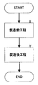
半導体装置は、多数のトランジスタやダイオード等の電子素子及びそれらの電子素子を電気的に接続する配線が形成された半導体チップ(例えば、厚み0.5mm、たて10mm、横8mm)が、その使用形態に応じたパッケージに封止されて、コンピュータ等の電子装置に組込み込まれ利用される。半導体装置の製造工程は、図2に示したマクロ製造工程フローように、多数の半導体チップが形成されるウェハを数十枚まとめて一括(ロット)製造する製造前工程Xと、ウェハに形成された半導体チップを個々に切り離し、パッケージに実装し製品検査する製造後工程Yからなる。FPLD(ディジタルIC)やフューズメモリ等の様に、製造後工程Y終了後にユーザが機能を決定する例外的な半導体装置もあるが、半導体装置の電気特性は、ウェハに半導体チップが形成された時点、言い換えれば製造前工程X終了時点でほぼ決定される。以下では製造後工程Y起因の特性変動は考えないものとする。従って、本明細書では、半導体装置の製造工程について製造前工程Xについてのみ説明し、製造後工程Yの説明は、非特許文献1に譲る。
A semiconductor device has a semiconductor chip (for example, a thickness of 0.5 mm, a length of 10 mm, and a width of 8 mm) on which a large number of electronic elements such as transistors and diodes and wirings for electrically connecting these electronic elements are formed. And is used by being incorporated into an electronic device such as a computer. As shown in the macro manufacturing process flow shown in FIG. 2, the semiconductor device manufacturing process is performed on the wafer, including a pre-manufacturing process X in which dozens of wafers on which a large number of semiconductor chips are formed are collectively manufactured (lot). It consists of a post-manufacturing process Y in which the semiconductor chips are individually separated, mounted in a package, and inspected. There are exceptional semiconductor devices such as FPLD (digital IC) and fuse memory where the user decides the function after completion of the post-manufacturing process Y, but the electrical characteristics of the semiconductor device are the same as when the semiconductor chip is formed on the wafer. In other words, it is almost determined at the end of the pre-manufacturing process X. In the following, it is assumed that the characteristic variation caused by the post-production process Y is not considered. Therefore, in the present specification, only the pre-manufacturing process X will be described for the manufacturing process of the semiconductor device, and the description of the post-manufacturing process Y will be left to Non-Patent
ここに、半導体装置の製造前工程Xを図3の一般的な製造工程フローを用いて説明する(例えば、非特許文献1参照。)。この半導体装置はCMOS半導体装置とも呼ばれる。 Here, the pre-manufacturing process X of the semiconductor device will be described with reference to the general manufacturing process flow of FIG. 3 (see, for example, Non-Patent Document 1). This semiconductor device is also called a CMOS semiconductor device.
1.フィールド酸化膜形成
半導体基板、P型半導体基板表面付近に部分的に膜厚の異なる絶縁膜を、熱酸化等により選択的に形成する(図3、工程J)。
1. Field oxide film formation An insulating film having a partially different film thickness is selectively formed near the surface of the semiconductor substrate or P-type semiconductor substrate by thermal oxidation or the like (FIG. 3, step J).
2.Nウェル形成
Nウェル形成用のPhos(リン)等を選択的に半導体基板表面にイオン注入しNウェルを形成する(図3、工程K)。
2. N-well formation Phos (phosphorus) or the like for N-well formation is selectively ion-implanted into the surface of the semiconductor substrate to form an N-well (FIG. 3, step K).
3.LOCOS分離
P型半導体基板表面付近にP型チャネルストッパー形成用のBF2等を選択的に半導体基板表面にイオン注入した後、LOCOS法等により選択的に素子分離用絶縁膜とチャネルストッパーを形成する(図3、工程L)。
3. LOCOS isolation BF 2 or the like for forming a P-type channel stopper is selectively implanted into the surface of the semiconductor substrate in the vicinity of the surface of the P-type semiconductor substrate, and then an element isolation insulating film and a channel stopper are selectively formed by the LOCOS method or the like. (FIG. 3, process L).
4.チャネルドープ
将来トランジスタを形成する素子形成用能動領域に選択的に閾値電圧制御用のPhos等を半導体基板表面にイオン注入し不純物注入領域を形成する(図3、工程M)。
4). Channel doping An impurity-implanted region is formed by selectively implanting a threshold voltage control Phos or the like into the active region for forming a transistor to form a transistor in the future on the surface of the semiconductor substrate (FIG. 3, step M).
5.ゲート酸化
素子形成用能動領域の半導体基板表面付近の酸化膜を除去し、熱酸化等によりゲート酸化膜を形成する(図3、工程N)。
5. The oxide film near the surface of the semiconductor substrate in the active region for forming the gate oxide is removed, and a gate oxide film is formed by thermal oxidation or the like (FIG. 3, step N).
6.ポリシリコンゲート
ゲート酸化膜上にCVD技術、フォトリソグラフィ技術、エッチング技術を用いて選択的にポリシリコンゲートを形成する(図3、工程O)。
6). Polysilicon gate A polysilicon gate is selectively formed on the gate oxide film by using a CVD technique, a photolithography technique, and an etching technique (FIG. 3, step O).
7.ソース/ドレイン形成
P型半導体基板表面にCVD法または熱酸化法により酸化膜を形成した後、素子形成用能動領域の所望領域にポリシリコンゲートと酸化膜に対してセルフアライメント的にソース/ドレイン(SD)形成用の不純物原子を半導体基板表面にイオン注入し、N型ソース領域とN型ドレイン領域、P型ソースとP型ドレイン領域を形成する(図3、工程P)。
7). Source / Drain Formation After an oxide film is formed on the surface of the P-type semiconductor substrate by CVD or thermal oxidation, the source / drain (self-aligned with respect to the polysilicon gate and oxide film in a desired region of the active region for element formation) SD) Impurity atoms for formation are ion-implanted into the surface of the semiconductor substrate to form an N-type source region and an N-type drain region, and a P-type source and a P-type drain region (FIG. 3, step P).
8.層間絶縁膜形成
P型半導体基板表面にCVD法等により酸化膜を堆積し層間絶縁膜を形成する(図3、工程Q)。
8). Formation of interlayer insulating film An oxide film is deposited on the surface of the P-type semiconductor substrate by a CVD method or the like to form an interlayer insulating film (FIG. 3, step Q).
9.コンタクトホール形成
層間絶縁膜163の所望の領域にフォトリソグラフィ技術、エッチング技術を用いて選択的にコンタクトホールを形成する(図3、工程R)。
9. Contact hole formation A contact hole is selectively formed in a desired region of the interlayer insulating film 163 by using a photolithography technique and an etching technique (FIG. 3, step R).
10.金属配線形成
層間絶縁膜上にスパッタ技術、フォトリソグラフィ技術、エッチング技術等を用いて選択的に金属配線を形成する(図3、工程S)。
10. Metal wiring formation Metal wiring is selectively formed on the interlayer insulating film by using a sputtering technique, a photolithography technique, an etching technique or the like (FIG. 3, step S).
11.保護膜
金属配線上に、保護膜270を堆積し、所望の領域(外部接続端子領域等の金属配線)を選択的に窓明けする(図3、工程T)。
11. Protective film A
12.ウェハ検査
ウェハプローバを介して半導体チップとICテスタを電気的に接続し、半導体装置の電気特性等を検査する(図3、工程U)。
12 Wafer inspection A semiconductor chip and an IC tester are electrically connected via a wafer prober to inspect the electrical characteristics and the like of the semiconductor device (FIG. 3, step U).
以上述べたように、半導体装置は長い製造工程を経て製造される。この製造工程は細かく見ると100ステップを遥かに越える複雑な製造工程である。 As described above, the semiconductor device is manufactured through a long manufacturing process. This manufacturing process is a complicated manufacturing process far exceeding 100 steps in detail.
C半導体装置の電気特性は、前記半導体チップに含まれる回路素子の特性により決定される。C半導体装置の代表的な回路素子であるトランジスタの非飽和時における電気特性は、よく知られているように式1で近似される。
The electrical characteristics of the C semiconductor device are determined by the characteristics of the circuit elements included in the semiconductor chip. As is well known, the electrical characteristics at the time of non-saturation of a transistor, which is a typical circuit element of a C semiconductor device, are approximated by
Id=μC(W/L)(Vg−Vt)Vd 式1
ここで、
Id: トランジスタのドレイン電流
μ: トランジスタのキャリア移動度
C: トランジスタの単位面積当ゲート容量
W: トランジスタのゲート長
L: トランジスタのゲート幅
Vg: トランジスタのゲート・ソース間電圧
Vd: トランジスタのドレイン・ソース間電圧
Vt: トランジスタの閾値電圧
式1により、トランジスタの電流特性は多くの特性パラメータで決定されることがわかる。更に、閾値電圧Vtは式2で決定される。
Id = μC (W / L) (Vg−Vt)
here,
Id: drain current of transistor
μ: Transistor carrier mobility
C: Gate capacity per unit area of transistor
W: Transistor gate length
L: Transistor gate width
Vg: Transistor gate-source voltage
Vd: Transistor drain-source voltage
Vt: threshold voltage of transistor According to
Vt=VF+2ΦF+(QA+QB)/C 式2
ここで、
VF:フラットバンド電圧
ΦF: 不純物によるフェルミ順位のシフト
QA: 酸化膜とシリコン表面の単位面積当界面電荷
QB: 空乏層の単位面積当電荷
C: トランジスタの単位面積当ゲート容量
前述の100ステップを越える製造工程で製造されるトランジスタの電気特性は、長い製造工程の影響で大きくばらつくことがある。半導体装置を商品化する場合は、このバラツキを考慮して品質とコストの兼ね合いで製品仕様を決定し、半導体装置の電気特性が製品仕様を満たすように回路設計する。しかし、市場の強い要求でコストを犠牲にして精度の良さという高品質を優先せざるを得ない場合がある。電気特性バラツキに敏感な特性パラメータ、例えば閾値電圧Vtは、ロット間はもとよりウェハ間やロット内、更に半導体チップ内でも大きなバラツキを生じることがある。閾値電圧Vtのような半導体装置の電気特性バラツキへの寄与率が大きいパラメータのバラツキを吸収し低減化する製造方法の実現が従来から望まれていた。
Vt = V F + 2Φ F + (Q A + Q B ) /
here,
V F : Flat band voltage
Φ F : Fermi rank shift due to impurities
Q A : Interfacial charge per unit area of oxide film and silicon surface
Q B : Charge per unit area of depletion layer
C: Gate capacity per unit area of transistor The electrical characteristics of a transistor manufactured in a manufacturing process exceeding 100 steps described above may vary greatly due to the influence of a long manufacturing process. When commercializing a semiconductor device, a product specification is determined in consideration of this variation in consideration of quality and cost, and a circuit design is performed so that the electrical characteristics of the semiconductor device satisfy the product specification. However, there is a case where high quality with high accuracy is prioritized at the expense of cost due to strong market demand. Characteristic parameters that are sensitive to variations in electrical characteristics, such as the threshold voltage Vt, may vary greatly not only between lots, but also between wafers, within lots, and even within semiconductor chips. Conventionally, it has been desired to realize a manufacturing method that absorbs and reduces variations in parameters such as the threshold voltage Vt that contribute greatly to variations in electrical characteristics of a semiconductor device.
従来から前記課題を解決する閾値電圧Vtのバラツキを低減化する半導体装置製造方法が提案されている。この製造方法は、例えば図2の一般的な製造工程フローに図14のバラツキを低減化する工程を追加したものである。前記バラツキを低減化する工程は、製造工程途中で製品の出来栄えを測定観測する出来栄え観測工程Fと、その観測情報を用いて、半導体装置の後続する製造工程に含まれるバラツキ低減工程Hの製造条件を設定する条件設定工程Gと、設定された製造条件で電気特性バラツキを吸収して半導体装置を製造するバラツキ低減工程Hを含む製造方法である。前記3工程は、前述のウェハ検査(図3、工程U)を拡張した工程とみなすことができる。 Conventionally, there has been proposed a semiconductor device manufacturing method for reducing variation in threshold voltage Vt that solves the above-described problems. In this manufacturing method, for example, a process for reducing the variation in FIG. 14 is added to the general manufacturing process flow in FIG. The process of reducing the variation is a production condition observation process F for measuring and observing the quality of the product during the production process, and manufacturing conditions of the variation reduction process H included in the subsequent production process of the semiconductor device using the observation information. Is a manufacturing method including a condition setting step G for setting and a variation reducing step H for manufacturing a semiconductor device by absorbing the variation in electrical characteristics under the set manufacturing conditions. The three steps can be regarded as an extension of the above-described wafer inspection (FIG. 3, step U).
前記課題を解決する第1の従来技術は、現行製造条件で製造中の半導体チップに含まれる電子素子の閾値電圧Vtを測定(またはシミュレーション)し、半導体装置の現行製造条件とその測定結果から、次ロット製造の次回製造条件を調節決定し半導体装置の閾値電圧Vtのバラツキを低減化し、電気特性バラツキを低減化するするフィードバック式製造方法である(例えば、特許文献1参照。)。前記課題を解決する第2の従来技術は、製造中の半導体チップに含まれる受動素子の値(例えば、抵抗値)を調節して閾値電圧Vtなどのバラツキをチップ毎に吸収し、半導体装置の電気特性バラツキを低減化するトリミング式製造方法である(例えば、特許文献2参照。)。これらの従来技術について以下簡単に説明するが、詳細な説明は特許文献に譲る。 The first conventional technique for solving the above problem is to measure (or simulate) the threshold voltage Vt of an electronic element included in a semiconductor chip being manufactured under the current manufacturing conditions, and from the current manufacturing conditions of the semiconductor device and the measurement results thereof, This is a feedback type manufacturing method that adjusts and determines the next manufacturing conditions for the next lot manufacturing, reduces the variation in the threshold voltage Vt of the semiconductor device, and reduces the variation in electrical characteristics (see, for example, Patent Document 1). A second conventional technique for solving the above problem is to adjust the value (for example, resistance value) of a passive element included in a semiconductor chip being manufactured to absorb variations such as a threshold voltage Vt for each chip, and This is a trimming manufacturing method that reduces variation in electrical characteristics (see, for example, Patent Document 2). These prior arts will be briefly described below, but the detailed description will be left to the patent literature.
製造バラツキを低減化させる従来の半導体装置製造方法であるフィードバック式製造方法は、新たに半導体装置を製造する場合に、製造工程の現行製造条件から次回製造条件を設定する方法である。すなわち、前記現行製造条件で製造された半導体製品の閾値電圧Vtを測定し、現在製造中の半導体装置の出来栄えを測定または評価し(図15、工程F)、次にあらかじめ準備された判定基準に則り次回製造条件を見直し決定し(図15、工程G)、前記次回製造条件で次回の半導体装置を製造する(図15、工程H)半導体装置の電気特性バラツキを低減化する製造方法である。このフィードバック式製造方法によると、現在のバラツキ情報により、次回の製造条件が調整され、半導体装置の電気特性バラツキが低減される。具体的な次回製造条件の決定方法を、図15に示した。 A feedback manufacturing method, which is a conventional semiconductor device manufacturing method that reduces manufacturing variations, is a method of setting next manufacturing conditions from current manufacturing conditions in a manufacturing process when a new semiconductor device is manufactured. That is, the threshold voltage Vt of the semiconductor product manufactured under the current manufacturing conditions is measured, and the performance of the semiconductor device currently being manufactured is measured or evaluated (FIG. 15, step F). Accordingly, the next manufacturing condition is reviewed and determined (FIG. 15, step G), and the next semiconductor device is manufactured under the next manufacturing condition (FIG. 15, step H). This is a manufacturing method for reducing variation in electrical characteristics of the semiconductor device. According to this feedback manufacturing method, the next manufacturing condition is adjusted based on the current variation information, and the variation in the electrical characteristics of the semiconductor device is reduced. A specific method for determining the next manufacturing condition is shown in FIG.
製造バラツキを低減化させる従来の他の半導体装置製造方法であるトリミング式製造方法は図18に示すようなトリミング回路を利用する。図18のトリミング回路では、外部入力端子300と外部入力端子301間に抵抗220と抵抗221が電気的に直列接続されており、抵抗220、221にはそれぞれヒューズ230、231が並列に接続され、さらに抵抗220と抵抗221との接続点にトランジスタ210のゲート電極が接続される。トランジスタ210のドレイン領域は内部回路240を介して外部入出力端子303に、ソース領域は内部回路241を介して外部入出力端子304に接続されている。本半導体装置のトリミング回路のヒューズ230、231は、例えばポリシリコンで形成されているが、アルミニウムなどの金属薄膜でもよい。ここで、抵抗220、221、ヒューズ230、231のペアは必要に応じて複数個設置される事がある。 A trimming type manufacturing method, which is another conventional semiconductor device manufacturing method for reducing manufacturing variation, uses a trimming circuit as shown in FIG. In the trimming circuit of FIG. 18, a resistor 220 and a resistor 221 are electrically connected in series between the external input terminal 300 and the external input terminal 301, and fuses 230 and 231 are connected in parallel to the resistors 220 and 221 respectively. Further, the gate electrode of the transistor 210 is connected to a connection point between the resistor 220 and the resistor 221. The drain region of the transistor 210 is connected to the external input / output terminal 303 via the internal circuit 240, and the source region is connected to the external input / output terminal 304 via the internal circuit 241. The fuses 230 and 231 of the trimming circuit of the semiconductor device are made of, for example, polysilicon, but may be a metal thin film such as aluminum. Here, a plurality of pairs of resistors 220 and 221 and fuses 230 and 231 may be provided as necessary.
トリミング式製造方法では、製造工程中で半導体装置の出来ばえを測定観測し(図16、工程F)、個々の半導体チップの電気特性バラツキを吸収するようにトリミング回路のヒューズ切断箇所を個々に決定し(図16、工程G)、個々の半導体装置をトリミングする(図16、工程H)半導体装置の電気特性バラツキを低減化する製造方法である。
しかしながら、この従来の製造方法では、以下のような課題を有していた。
図15の従来技術であるフィードバック式製造方法では、はじめに新たな製造工程の初期条件を現行製造工程(既存技術)から類推、引用等の方法で設定し、次に前記初期製造条件で全工程による試作またはシミュレーションを行い、次に出来栄えを測定または観測し、次にあらかじめ準備された判定基準に則り初期製造条件を見直し、次回製造条件を決定するので、出来栄えを測定する工程F及び製造条件を決定する工程Gを現在製造中の半導体装置に適用できない。製造済み半導体装置のウェハ検査結果を次回の製造条件改善にフィードバックし製造工程の改善は実現できるが、製造工程中の半導体装置の直接的なバラツキ低減化には寄与しないという課題を有していた。
However, this conventional manufacturing method has the following problems.
In the feedback type manufacturing method of FIG. 15 which is the prior art, first, initial conditions for a new manufacturing process are set by a method such as analogy and citation from the current manufacturing process (existing technology), and then the initial manufacturing conditions depend on all processes. Prototype or simulation, then measure or observe the performance, then review the initial manufacturing conditions according to the criteria prepared in advance and determine the next manufacturing conditions, so determine the process F and manufacturing conditions to measure the performance The process G to be applied cannot be applied to a semiconductor device currently being manufactured. Although the wafer inspection result of the manufactured semiconductor device can be fed back to the next manufacturing condition improvement to improve the manufacturing process, there has been a problem that it does not contribute to the direct variation reduction of the semiconductor device during the manufacturing process. .
図16の従来技術であるトリミング式製造方法では、製造工程途中の半導体装置そのものを測定するで、出来栄えを測定する工程F及び製造条件を決定する工程Gを現在製造中の半導体装置に適用できる。しかしこの方法では、測定時(ほとんどの場合接触型の測定であるため)に半導体装置に及ぼす品質ダメージや、事前に半導体装置内に測定結果を反映させるトリミング回路を設けるため、この冗長回路によって半導体装置のチップ面積が増加することによる量産効率の低下があり、コストの上昇を招いていた。
本発明は、半導体装置のチップ面積を増大させることなしに、製造中の半導体装置のバラツキを低減させる製造方法を提供することを目的としている。
In the conventional trimming manufacturing method of FIG. 16, the semiconductor device itself during the manufacturing process is measured, so that the process F for measuring the quality and the process G for determining the manufacturing conditions can be applied to the semiconductor device currently being manufactured. However, in this method, the redundant circuit is used to provide a trimming circuit that reflects the quality damage to the semiconductor device during measurement (since it is mostly a contact type measurement) and the measurement result in the semiconductor device in advance. There was a decrease in mass production efficiency due to an increase in the chip area of the device, leading to an increase in cost.
An object of the present invention is to provide a manufacturing method that reduces variations in a semiconductor device being manufactured without increasing the chip area of the semiconductor device.
製品となる半導体装置を形成するウェハ(以後、本体ウェハと称す。)を製造する製造前工程X(以後、本体ウェハ製造工程と称する。)と、モニタ素子200を形成するウェハ(以後、モニタウェハと称す。)を製造するモニタウェハ製造工程(図1、工程Z)からなる半導体製造方法であって、本体ウェハ製造工程Xとモニタウェハ製造工程Zが、半導体装置の出来栄えをモニタ素子200にコピーするモニタリング工程(図1、工程C)を共有し、本体ウェハ製造工程Xは、モニタリング工程C後にバラツキ低減工程(図1、工程H)を含み、モニタ製造工程Zは、モニタリング工程C後にモニタ素子200の特性を測定する出来栄え観測工程(図1、工程F)とそれに続く観測情報でバラツキ低減工程Hの製造条件を設定する条件設定工程(図1、工程G)を含む半導体製造方法とした。この半導体製造方法をここでは、フィードフォワード式製造方法と称する。
A pre-manufacturing process X (hereinafter referred to as a main body wafer manufacturing process) for manufacturing a wafer (hereinafter referred to as a main body wafer) for forming a semiconductor device as a product, and a wafer for forming a monitor element 200 (hereinafter referred to as a monitor wafer). Is a semiconductor manufacturing method comprising a monitor wafer manufacturing process (FIG. 1, process Z), and the main body wafer manufacturing process X and the monitor wafer manufacturing process Z copy the performance of the semiconductor device to the
本発明の実施形態は後程詳細に説明するが、図1のように製造工程途中において半導体装置のバラツキ状態をモニタ素子200(図4)にコピーして(図1、工程C)、製造中の半導体装置の出来栄えを観測し(図1、工程F)その観測情報から半導体装置の完成時の出来栄えを推定し(図1、工程G1)、その推定情報に応じて後続する製造工程に含まれるバラツキ低減工程の製造条件をアナログ的に設定し(図1、工程G2)設定された製造条件で電気特性バラツキを低減して製造中の半導体装置を製造する(図1、工程H)ので、製造中の半導体装置の電気特性バラツキを大幅に低減化させることができる。すなわち、本発明によれば、製品となる半導体装置への品質ダメージは無く、冗長回路も必要とせずに、半導体装置のバラツキを低減させることができる。 The embodiment of the present invention will be described in detail later. As shown in FIG. 1, the variation state of the semiconductor device is copied to the monitor element 200 (FIG. 4) during the manufacturing process (FIG. 1, step C). The performance of the semiconductor device is observed (FIG. 1, process F), and the performance at the time of completion of the semiconductor device is estimated from the observed information (FIG. 1, process G1), and the variation included in the subsequent manufacturing process according to the estimated information The manufacturing conditions of the reduction process are set in an analog manner (FIG. 1, step G2), and the semiconductor device being manufactured is manufactured by reducing the electrical characteristic variation under the set manufacturing conditions (FIG. 1, step H). The variation in electrical characteristics of the semiconductor device can be greatly reduced. In other words, according to the present invention, there is no quality damage to a semiconductor device as a product, and the redundancy of a semiconductor device can be reduced without requiring a redundant circuit.
更に、半導体装置の出来栄えを増幅コピーするモニタ素子200を、長い工程を経る本体ウェハと異なる短い工程を経るモニタウェハ上に形成し利用することにより、短時間で安価なモニタリングが可能となり、質及び量とも高い観測情報が得られるので、出来栄え測定工程Fの製造条件をより正確に設定できる。よって、本発明のフィードフォワード式製造方法は、半導体装置の電気特性バラツキを一層低減化させることができ、半導体装置を高品質、高歩留で製造できる半増体装置製造方法を実現することができる。
Furthermore, by forming and using the
図1は、本発明による半導体装置の製造方法の製造工程フローの概念図である。本発明実施例の製造方法は、製品となる半導体装置を形成するウェハを製造する本体ウェハ製造工程Xと、モニタ素子200を形成するウェハ(以後、モニタウェハを製造するモニタウェハ製造工程Zからなる。本体ウェハ製造工程Xとモニタウェハ製造工程Zは、モニタリング工程Cのみを共有する。モニタリング工程Cは、本体ウェハに形成される半導体装置の出来栄えをモニタウェハに形成されるモニタ素子200にコピーする重要な工程である。
FIG. 1 is a conceptual diagram of a manufacturing process flow of a semiconductor device manufacturing method according to the present invention. The manufacturing method of the embodiment of the present invention includes a main body wafer manufacturing process X for manufacturing a wafer for forming a semiconductor device as a product, and a wafer for forming a monitor element 200 (hereinafter, a monitor wafer manufacturing process Z for manufacturing a monitor wafer). The main wafer manufacturing process X and the monitor wafer manufacturing process Z share only the monitoring process C. The monitoring process C copies the quality of the semiconductor device formed on the main wafer to the
本体ウェハ製造工程Xには、基本的には製造工程フロー(図3)を利用することができる。図1に示すモニタリング工程Cは必要に応じて図3の製造工程フローの中から選定される。このモニタリング工程Cは、複数工程選定しても良い。ここで、仮に一般的な製造工程フロー(図3)の中からモニタリング工程Cと指定された工程、例えばゲート酸化膜工程N以前の工程を本体前処理工程Bと称し、モニタリング工程C以後の後続する製造工程を本体後処理工程Dと称する。本体後処理工程Dにはバラツキ低減工程Hが含まれる。バラツキ低減工程Hは、モニタリング工程Cに対応して必要ならば複数工程設定する。後続前処理工程D1と後続後処理工程D2は、必要に応じてバラツキ低減工程Hの前後に図3の製造工程フローの中から選定される。 For the main body wafer manufacturing process X, a manufacturing process flow (FIG. 3) can be basically used. The monitoring process C shown in FIG. 1 is selected from the manufacturing process flow of FIG. 3 as necessary. This monitoring process C may be selected from a plurality of processes. Here, a process designated as a monitoring process C in a general manufacturing process flow (FIG. 3), for example, a process before the gate oxide film process N is referred to as a main body pretreatment process B, and a subsequent process after the monitoring process C. This manufacturing process is referred to as a main body post-processing process D. The main body post-processing step D includes a variation reducing step H. The variation reduction process H is set in accordance with the monitoring process C if necessary. The subsequent preprocessing step D1 and the subsequent postprocessing step D2 are selected from the manufacturing process flow of FIG. 3 before and after the variation reducing step H as necessary.
本発明の実施例に適用した半導体装置の製造前工程Xを、工程順断面図(図5〜13、図19)を用いて詳細に説明する。本発明の実施例は、前記の工程順断面図に限定されるものではなく、一般的な半導体装置の製造前工程に適用できる。勿論、MOS半導体装置に限定されるものではなく、バイポーラ半導体装置や化合物半導体等の製造方法に適用することもできる。 The pre-manufacturing process X of the semiconductor device applied to the embodiment of the present invention will be described in detail with reference to cross-sectional views in the order of processes (FIGS. 5 to 13 and FIG. 19). The embodiments of the present invention are not limited to the above-described cross-sectional views in the order of processes, and can be applied to general processes for manufacturing semiconductor devices. Of course, the present invention is not limited to a MOS semiconductor device, and can be applied to a manufacturing method of a bipolar semiconductor device, a compound semiconductor, or the like.
1.フィールド酸化膜
半導体基板例えば、P型半導体基板102表面付近に部分的に膜厚の異なる絶縁膜を熱酸化等により選択的に形成し300nm〜1000nm程度の酸化膜103と50nm〜100nm程度の酸化膜104を得る。ここではP型の半導体基板を用いたが、N型の半導体基板板も用いることができる。(図5)
2.Nウェル
Nウェル111は、本体ウェハ表面にイオン注入法により不純物、たとえばリンを3.0×10¹²/cm2程度の不純物量を注入し、ウェル不純物注入領域を形成する。これをウェル不純物注入工程という。次に、イオン注入法により本体ウェハに添加された不純物は、そのままでは電気的に不活性なので熱処理による活性化、及び注入時のダメージを回復させる。さらに、Nウェル111内にPMOSトランジスタを作りこむためには、ある程度深さを持ったNウェル111としなければならず、一般的には、微細化されたトランジスタにおいては1〜3mm、高耐圧のトランジスタについては3〜8mm程度の深さとなる。この熱処理において必要な不純物の分布(プロファイル)を得るため、例えば電気炉により1100〜1200℃で数時間〜十数時間の条件で熱拡散をする。これをウェル熱拡散工程という。(図6)。ウェル熱拡散工程は複数枚(150枚程度)の大口径ウェハを同時に高温で長時間処理される。ここではNウェル111を用いたが、Pウェルまたは両方のウェルを用いることができる。
1. Field oxide film Semiconductor substrate For example, an insulating film having a partially different thickness near the surface of a P-
2. N well N well 111 forms a well impurity implantation region by implanting an impurity amount of about 3.0 × 10 12 / cm 2 into the surface of the main wafer by an ion implantation method. This is called a well impurity implantation step. Next, since the impurities added to the main wafer by the ion implantation method are electrically inactive as they are, activation by heat treatment and damage during implantation are recovered. Further, in order to build a PMOS transistor in the N well 111, the N well 111 must have a certain depth. Generally, a miniaturized transistor has a high breakdown voltage of 1 to 3 mm. Is about 3-8mm deep. In order to obtain a necessary impurity distribution (profile) in this heat treatment, for example, heat diffusion is performed at 1100 to 1200 ° C. for several hours to tens of hours in an electric furnace. This is called a well thermal diffusion process. (FIG. 6). In the well thermal diffusion process, a plurality of (about 150) large-diameter wafers are simultaneously processed at a high temperature for a long time. Although the N well 111 is used here, a P well or both wells can be used.
3.LOCOS
P型半導体基板102表面付近に選択的にP型チャネルストッパー142形成用のB、BF2等を選択的に半導体基板表面にイオン注入した後、LOCOS法等により選択的に素子分離用絶縁膜130、P型チャネルストッパー142を形成する(図7)。ここでLOCOS法を用いて素子分離用酸化膜を形成する場合、熱酸化工程は複数枚(150枚程度)の大口径ウェハを同時に高酸化レートで、高温で長時間処理される。
3. LOCOS
After selectively ion-implanting B, BF 2 or the like for forming the P-
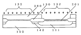
4.チャネルドープ
将来MOSトランジスタが形成される素子形成用能動領域132に選択的に閾値電圧制御用のPhos、As、B、BF2等を半導体基板表面にイオン注入し不純物注入領域201が形成される。不純物注入領域201が形成される領域はMOSトランジスタの導電型、閾値電圧、等必要に応じて複数領域別々に形成される場合があり、半導体装置の仕様によりイオン注入量等の許容範囲が著しく狭い場合もある(図8)。本チャネルドープ工程Mは、次のゲート酸化膜工程Nの後に行っても、同様な半導体装置が得られる。
4). Channel dope Phos, As, B, BF 2 and the like for controlling the threshold voltage are selectively ion-implanted into the surface of the semiconductor substrate in the element formation
5.ゲート酸化
素子形成用能動領域132の半導体基板表面付近の酸化膜を除去し、熱酸化等によりゲート酸化膜161を形成する(図9)。ここでゲート酸化膜161の膜厚は半導体装置の仕様により様々であるが、MOSトランジスタの閾値電圧を決定する重要なプロセスパラメータである。さらにこの後(ゲート酸化膜161形成後)図8で説明した将来MOSトランジスタが形成される素子形成用能動領域132に選択的に閾値電圧制御用のPhos、B、BF2等を半導体基板表面にイオン注入し不純物注入領域201を形成する場合もある。
5. The oxide film near the surface of the semiconductor substrate in the
6.ポリシリコン
ゲート酸化膜161上にCVD技術、フォトリソグラフィ技術、エッチング技術を用いて選択的にポリシリコンゲート170が形成される(図10)。ここでポリシリコンゲート170の加工幅は半導体装置の仕様により様々であるが、MOSトランジスタの駆動能力を決定する重要なプロセスパラメータである。また、ここでは図示していないが、この後、酸化膜を形成した後、抵抗用の第2層のポリシリコン層を形成する場合がある。
6). A
7.ソース/ドレイン形成
P型半導体基板102表面にCVD法または熱酸化法により酸化膜164を形成した後、素子形成用能動領域132の所望の領域にポリシリコンゲート170と酸化膜164に対してセルフアライメント的にソース、ドレイン形成用のPhos、As、B、BF2等を半導体基板表面にイオン注入しN型ソース領域181、N型ドレイン領域191、P型ソース領域182、P型ドレイン領域192が形成される。(図11)。ここで、それぞれのソース、ドレインはLDD(Lightly Doped Drain)と呼ばれる低濃度の不純物領域を有する構造やDDD(Double Diffused Drain)と呼ばれる900℃〜1100℃程度、窒素または希釈酸素雰囲気で拡散する事により形成された低濃度の不純物領域を有する構造を用いる場合がある。これに本ソース/ドレイン形成工程Pでソース/ドレインを形成する前に、イオン注入された不純物を900℃〜1100℃程度、窒素または希釈酸素雰囲気で熱拡散する事により形成された低濃度不純物領域134を有する構造を用いる場合がある(図19)。この工程を、以後DDD工程と称す。
7). Source / Drain Formation After an
8.層関絶縁膜
P型半導体基板102表面にCVD法等により酸化膜を堆積し、800〜900℃程度の希釈酸素雰囲気でアニールし、層間絶縁膜163を形成する(図12)。
8). Interlayer insulating film An oxide film is deposited on the surface of the P-
9.コンタクト、金属配線、保護膜
層間絶縁膜163の所望の領域にフォトリソグラフィ技術、エッチング技術を用いて選択的にコンタクトホール250を形成し、ウェットエッチングまたはリフロー等でコンタクトホールの形状を滑らかに成形する。スパッタ技術、フォトリソグラフィ技術、エッチング技術等を用いて選択的に金属配線260を形成し、CVD法等により保護膜270を堆積し、所望の領域(外部接続端子領域等)を選択的に窓明けする。ここでは単層の金属配線260を形成する場合について記述したが、この金属配線は層間絶縁膜を介して複数の積層構造が形成される場合もある。また、金属配線はバリア金属を下層に、反射防止膜を上層に有する構造の場合もある。さらに、プロセスダメージ回復用の350℃〜450℃、水素雰囲気でのアニール工程が含まれる場合もある(図13)。
9. Contact, metal wiring, protective film A contact hole 250 is selectively formed in a desired region of the interlayer insulating film 163 using a photolithography technique or an etching technique, and the shape of the contact hole is smoothly formed by wet etching or reflow. . A
本発明の特徴であるモニタウェハ製造工程Zは、モニタウェハを前処理し(図1、工程A)、本体ウェハと同時処理により本体ウェハの特性をコピーし(図1、工程C)、モニタ素子200を後処理し(図1、工程E)、モニタ素子200の特性を測定し(図1、工程F)、バラツキ低減工程Hの製造条件を決定(図1、工程G)する工程からなる。ここで、本体ウェハの製造途中の出来栄えをモニタウェハへコピーするモニタリング工程Cは、本体ウェハとモニタウェハを同一の装置内で同時に処理する。本実施例では、モニタリング工程Cで半導体装置の製造途中の出来栄えをコピーするモニタ素子200として、図4に示すMOSダイオードを利用する。以下、モニタウェハ製造工程Zを中心に、本発明フィードフォワード製造方法の実施例について詳細に説明する。
The monitor wafer manufacturing process Z, which is a feature of the present invention, pre-processes the monitor wafer (FIG. 1, step A), copies the characteristics of the main body wafer simultaneously with the main body wafer (FIG. 1, step C), and monitors the monitor element. 200 includes post-processing (FIG. 1, step E), measuring the characteristics of the monitor element 200 (FIG. 1, step F), and determining manufacturing conditions for the variation reduction step H (FIG. 1, step G). Here, in the monitoring step C for copying the quality of the main body wafer during manufacture to the monitor wafer, the main body wafer and the monitor wafer are simultaneously processed in the same apparatus. In the present embodiment, the MOS diode shown in FIG. 4 is used as the
1.モニタ前処理工程
モニタウェハは本体の半導体装置のP型半導体基板102より10%〜50%程度低濃度のP型半導体基板102とする。P型半導体基板102の表面付近にしきい値電圧制御用のPhos、As、B、BF2等を半導体基板表面にイオン注入し不純物注入領域を形成する。ここでのイオン注入工程は、処理状態を予測する半導体装置と同一条件で処理される事が望ましい。これは、イオン注入工程でのバラツキをより低減化させるためである。また、ここで低濃度の半導体基板を使用する理由はモニタリング感度をより高めるためである。ここで、モニタウェハのモニタリング工程C以前の製造工程は、本体ウェハのモニタリング工程C以前の製造工程より簡略化された製造工程であることが好ましい。具体的には、本実施例のモニタ前処理工程は、本体前処理工程Bに比べてNウェル工程KやLOCOS工程Lが省略され、簡便で短期間なものがコスト的に好ましい。モニタウェハの基板の濃度に関しても、必ずしも本体半導体装置より低濃度の半導体基板を用意する必要はなく、コストと測定精度の兼ね合いから決定すればよい。(図1、工程A)
2.モニタリング工程
このモニタリング工程Cは、製造による本体ウェハの出来栄えをモニタウェハにコピーする重要な工程である。すなわち、半導体製造装置完成時の出来栄えを左右する前記寄与大パラメータを予測できる工程影響(モニタ状況)をモニタウェハに正確にコピーする工程である。本実施例では、モニタリング工程Cとして、製造バラツキの大きいゲート酸化膜161を形成するゲート酸化膜工程Nとする。ゲート酸化膜工程Nは複数枚(150枚程度)の大口径ウェハを並べて同時に850℃〜1000℃程度の高温で長時間処理するため、ウェハ間、ウェハ内で熱履歴に差が生じ、大きな製造バラツキを発生させる可能性が高い工程である。製造バラツキはゲート酸化膜161の膜厚とゲート酸化膜161下の不純物注入領域201の不純物濃度プロファイルのバラツキにより生じ、製造前工程X終了時に、MOSトランジスタの閾値電圧Vtのバラツキとして顕在化する。モニタウェハを、本体前工程処理Bを経た本体ウェハと同時に処理する。同時に処理というのは、前記工程影響をより正確にコピーするためと言うことで、本体ウェハとモニタウェハの処理条件が同一であれば、本体ウェハとモニタウェハの同時処理は本発明の必要条件ではない。これはコピー精度の問題で、前記工程影響をより正確にコピーするためには、同時処理が好ましい。同様に、モニタウェハは、バラツキ許容範囲とゲート酸化工程のバラツキ範囲との相関関係で、挿入位置や挿入枚数が決定される。(図1、工程C)
3.モニタ後処理工程
本体ウェハと同時に処理(図1、工程C)されたモニタウェハのモニタ状態を増幅して高感度で測定できるようにモニタウェハの後処理(図1、工程E)は、形成されたゲート酸化膜161上にさらに第2ゲート酸化膜165を800℃〜850℃程度の熱酸化法または600℃〜800℃程度以下のCVD法でゲート酸化膜161の0.5倍〜1.5倍程度の膜厚で形成し、第2ゲート酸化膜165上にCVD法によりポリシリコンゲート170を形成する。ここで、第2ゲート酸化膜165はモニタリング感度を増幅するために形成したものである。調整が必要なVtは式2の様にQB/C(QB:不純物による電荷量、C:ゲート酸化膜容量値)の関数であるためゲート酸化膜厚が厚いほど不純物濃度プロファイルの変動(QBの変動)を高感度に増幅して測定できる。ただしこの場合、膜厚バラツキに比べて不純物濃度プロファイルのバラツキが大きい場合に効果がある。このゲート酸化工程において、ゲート膜厚のバラツキが大きい場合、第2ゲート酸化膜165は形成しない事が望ましい。またここではゲート電極をポリシリコンゲート170で形成しているが、金属、例えばアルミシリコンで形成する場合もある。また、追加される第2ゲート酸化膜165の形成温度、時間は、本体の半導体装置のゲート酸化膜工程N以降の熱履歴と類似させると、より高感度に不純物濃度プロファイルを検出できる。(図1、工程E)
本体の半導体装置のゲート酸化膜工程N以降の比較的高温の熱履歴は、前述したように次の6種類の工程が想定される。
(1)ポリシリコンゲート170(CVD法等で形成)
(2)酸化膜164(CVD法または熱酸化法により形成)、
(3)低濃度の不純物領域(DDD構造を用いる場合の900℃〜1100℃程度、窒素または希釈酸素雰囲気で拡散)、
(4)層間絶縁膜163(CVD法等により酸化膜を堆積し、800℃〜900℃程度、希釈酸素雰囲気でアニール)、
(5)形状滑らかなコンタクトホール(リフローで成形する場合)、
(6)プロセスダメージ回復(350℃〜450℃、水素雰囲気でのアニール工程)
前述した「本体の半導体装置のゲート酸化膜工程N以降の熱履歴を類似させる」とは、比較的高温が印可される工程の内、最も高温で長時間処理される(3)の工程での最高温度および処理時間の履歴を同一にさせることである。特に温度の高い複数の工程を選択する場合もある。これは、不純物拡散は主に温度による効果が大きいためである。つまりここでは、追加される第2ゲート酸化膜165の形成温度、時間は、低濃度の不純物領域(DDD構造を用いる場合の900℃〜1100℃程度、3〜5時間、窒素または希釈酸素雰囲気で拡散)形成工程と熱履歴を類似させることが望ましいことになる。
1. Pre-monitoring process The monitor wafer is a P-
2. Monitoring process This monitoring process C is an important process for copying the quality of the main wafer produced by the manufacturing to the monitor wafer. That is, it is a process of accurately copying the process influence (monitor situation) on the monitor wafer that can predict the large contribution parameter that affects the quality of the semiconductor manufacturing apparatus when it is completed. In this embodiment, the monitoring process C is a gate oxide film process N for forming a
3. Monitor post-processing process The monitor wafer post-process (FIG. 1, step E) is formed so that the monitor state of the monitor wafer processed simultaneously with the main body wafer (FIG. 1, step C) can be amplified and measured with high sensitivity. A second
As described above, the following six types of processes are assumed for the relatively high-temperature thermal history after the gate oxide film process N of the semiconductor device of the main body.
(1) Polysilicon gate 170 (formed by CVD method, etc.)
(2) Oxide film 164 (formed by CVD or thermal oxidation),
(3) Low-concentration impurity region (diffusion in a nitrogen or diluted oxygen atmosphere at about 900 ° C to 1100 ° C when using the DDD structure),
(4) Interlayer insulating film 163 (an oxide film is deposited by a CVD method or the like, and annealed in a diluted oxygen atmosphere at about 800 ° C. to 900 ° C.),
(5) Contact hole with smooth shape (when reflow molding),
(6) Process damage recovery (annealing process in a hydrogen atmosphere at 350 ° C to 450 ° C)
The above-mentioned “similar thermal history after the gate oxide film process N of the semiconductor device of the main body” is the process (3) in which the process is performed at the highest temperature for a long time among the processes where a relatively high temperature is applied. It is to make the history of the maximum temperature and processing time the same. In some cases, a plurality of processes having particularly high temperatures may be selected. This is because impurity diffusion is mainly due to temperature. That is, here, the temperature and time for forming the second
4.出来栄え測定工程
次に、モニタ素子200の工程影響を観測(工程F)する。本実施例では、モニタウェハのモニタ素子200のCV特性から不純物注入領域201の不純物濃度プロファイルのバラツキを求め、閾値電圧Vtまたはフラットバンド電圧Vfなどの観測情報を得る。(図1、工程F)
5.特性推定工程
前記観測情報から各ウェハに多数搭載されている半導体装置のゲート酸化膜厚と不純物濃度プロファイルを推定し、あらかじめ明らかにされているモニタウェハの閾値電圧Vtと本体ウェハに形成されるトランジスタの閾値電圧Vtとの相関関係から本体ウェハの閾値電圧Vtを推定する推定情報を作成する。(図1、工程G1)
6.条件決定工程
本実施例では、バラツキ低減工程Hとして本体後処理工程Dのチャネルドープ工程Mを選定する。前推定情報に応じて前記閾値電圧Vtのバラツキを十分に低減できるように、チャネルドープ工程Mのイオン注入条件をアナログ的に決定する。前記推定情報やモニタウェハの設置場所および枚数に応じて、ウェハ1枚毎または複数ウェハ毎にチャネルドープ工程Mのイオン注入条件を決定する。(図1、工程G2)
7.バラツキ低減工程
モニタリング工程Cを経た本体ウェハは、条件決定工程G2で決定したイオン注入条件で、ウェハ1枚毎または複数ウェハ毎に本体ウェハのチャネルドープ処理が実施される。(図1、工程H)
8.後続後処理工程
バラツキ低減工程Hを経た本体ウェハは、ウェハ検査工程Uを含む後続後処理工程を経て製造前工程Xは終了する。
4). Performance measurement process Next, the process influence of the
5. Characteristic estimation step The gate oxide film thickness and impurity concentration profile of a large number of semiconductor devices mounted on each wafer are estimated from the observation information, and the threshold voltage Vt of the monitor wafer and the transistor formed on the main wafer are clarified in advance. Estimated information for estimating the threshold voltage Vt of the main wafer is created from the correlation with the threshold voltage Vt of the main wafer. (FIG. 1, step G1)
6). Condition Determination Step In this embodiment, the channel doping step M of the main body post-processing step D is selected as the variation reduction step H. The ion implantation conditions of the channel doping process M are determined in an analog manner so that the variation in the threshold voltage Vt can be sufficiently reduced according to the previous estimation information. The ion implantation conditions for the channel dope process M are determined for each wafer or for each of a plurality of wafers according to the estimated information and the location and number of monitor wafers. (FIG. 1, step G2)
7). Dispersion reduction process The main body wafer that has undergone the monitoring process C is subjected to channel doping of the main body wafer for each wafer or a plurality of wafers under the ion implantation conditions determined in the condition determination process G2. (Fig. 1, Process H)
8). Subsequent Post-Processing Step For the main body wafer that has undergone the variation reducing process H, the pre-manufacturing process X is completed through the subsequent post-processing process including the wafer inspection process U.
以上の説明で明らか様に、モニタリング工程Cは本体ウェハの出来栄えをモニタウェハへ正確にコピーする工程であるが、ウェハ前処理工程Aおよびモニタ後処理工程Eは、コピーした出来栄えのバラツキを増幅して観測できるようにモニタ素子200を形成する工程でなければならない。
As is clear from the above description, the monitoring process C is a process of accurately copying the performance of the main body wafer to the monitor wafer, but the wafer pre-processing process A and the monitor post-processing process E amplify the variations in the copied performance. It is necessary to form the
ここでは、本実施例では、モニタリング工程Cをゲート酸化膜工程Nとして説明したが、同様の考え方を用いて、半導体装置の電気特性バラツキの原因になるLOCOS工程L、ポリシリコンゲート工程O、チャネルドープ工程M、前記DDD工程を含むソース/ドレイン形成工程P、各種エッチング工程をモニタリング工程Cとして適用可能である。また、バラツキ低減工程Hも、チャネルドープ工程Mとして説明したが、保護膜工程Tや前記DDD工程を含むソース/ドレイン工程P等をバラツキ低減工程Hとすることができる。モニタリング工程Cやバラツキ低減工程Hは、プロセスの特性を考慮して選定するのが良い。また、モニタリング工程Cやバラツキ低減工程Hを複数設定することができるが、これはコストを考慮して設定するのが良い。また、製造工程でのダメージ発生工程とダメージ回復工程でも本発明は活用できる。 Here, in this embodiment, the monitoring process C is described as the gate oxide film process N. However, using the same concept, the LOCOS process L, the polysilicon gate process O, the channel causing the variation in the electrical characteristics of the semiconductor device are described. The doping process M, the source / drain forming process P including the DDD process, and various etching processes can be applied as the monitoring process C. Further, although the variation reducing process H has been described as the channel doping process M, the source / drain process P including the protective film process T and the DDD process can be used as the variation reducing process H. The monitoring process C and the variation reducing process H are preferably selected in consideration of process characteristics. In addition, a plurality of monitoring processes C and variation reduction processes H can be set, but this should be set in consideration of cost. The present invention can also be used in a damage generation process and a damage recovery process in the manufacturing process.
本発明は、一般の半導体装置の製造に適用することを目的としているので広い範囲で用いることができる。例えば、高電圧動作が要求されるトランジスタと、低電圧低電流動作が要求されるトランジスタを共に含む半導体装置、具体的にはリチウムイオン電池の充放電を制御する電源マネージメント用半導体装置の製造に適用することにより、高品質で低コストの半導体を実現する本発明の効果を十分に発揮することができるが、これに限るものでないことは言うまでもない。 Since the present invention is intended to be applied to the manufacture of general semiconductor devices, it can be used in a wide range. For example, it is applicable to the manufacture of semiconductor devices that include both transistors that require high-voltage operation and transistors that require low-voltage and low-current operation, specifically, power management semiconductor devices that control the charging and discharging of lithium-ion batteries. By doing so, the effect of the present invention for realizing a high-quality and low-cost semiconductor can be sufficiently exhibited, but it goes without saying that the present invention is not limited to this.
102 P型半導体基板
103 酸化膜
104 酸化膜
111 Nウェル
130 素子間分離用絶縁膜
132 素子形成用能動領域
134 低濃度不純物領域
142 P型チャネルストッパー
161 ゲート酸化膜
162 ゲート電極
163 層間絶縁膜
164 酸化膜
165 第2ゲート酸化膜
170 ポリシリコンゲート
180 ソース領域
181 N型ソース領域
182 P型ソース領域
190 ドレイン領域
191 N型ドレイン領域
192 P型ドレイン領域
200 モニタ素子
201 不純物注入領域
210 トランジスタ
220、221 抵抗
230、231 ヒューズ
240、241 内部回路
250 コンタクトホール
260 金属配線
270 保護膜
300、301、303、304 外部入出力端子
102 P-
Claims (10)
モニタリング工程であるゲート酸化膜工程と、
前記モニタリング工程に後続する本体後処理工程に含まれるバラツキ低減工程として閾値電圧制御用の不純物をイオン注入し不純物注入領域を形成するチャネルドープ工程を有し、
モニタ素子が形成されるモニタウェハを製造するモニタウェハ製造工程は、
モニタ前処理工程と、
前記モニタウェハを前記本体ウェハと同一の装置内で、同時に同条件で処理する前記モニタリング工程と、
モニタ後処理工程と、
前記モニタリング工程を経て形成された前記モニタ素子のCV特性を測定する出来栄え観測工程と、
前記出来栄え観測工程において測定された前記モニタリング工程による工程影響から、前記バラツキ低減工程の製造条件としてイオン注入条件を決定する条件設定工程と、
を有し、
前記本体ウェハ製造工程と前記モニタウェハ製造工程は前記モニタリング工程のみを共有し、
前記チャネルドープ工程は、前記条件設定工程において決定された前記イオン注入条件により、前記本体ウェハに対して実施される半導体装置の製造方法。 A main body wafer manufacturing process including a plurality of processes for manufacturing a main body wafer on which a semiconductor device is formed,
A gate oxide film process which is a monitoring process;
A channel doping step of forming an impurity implantation region by ion implantation of impurities for threshold voltage control as a variation reducing step included in the main body post-processing step subsequent to the monitoring step;
The monitor wafer manufacturing process for manufacturing the monitor wafer on which the monitor element is formed is
Monitor pretreatment process;
The pre-Symbol monitor wafer in the body wafer and the same apparatus, and the monitoring step of treating the same conditions at the same time,
Post-monitoring process;
A performance observation step of measuring CV characteristics of the monitor element formed through the monitoring step;
From the process influence by the monitoring process measured in the performance observation process, a condition setting process for determining ion implantation conditions as manufacturing conditions of the variation reducing process ,
Have
The main body wafer manufacturing process and the monitor wafer manufacturing process share only the monitoring process,
The channel doping step is a method for manufacturing a semiconductor device, which is performed on the main wafer according to the ion implantation conditions determined in the condition setting step.
モニタリング工程であるゲート酸化膜工程と、
前記モニタリング工程に後続する本体後処理工程に含まれるバラツキ低減工程として層間絶縁膜形成工程における高温処理工程を有し、
モニタ素子が形成されるモニタウェハを製造するモニタウェハ製造工程は、
モニタ前処理工程と、
前記モニタウェハを前記本体ウェハと同一の装置内で、同時に同条件で処理する前記モニタリング工程と、
モニタ後処理工程と、
前記モニタリング工程を経て形成された前記モニタ素子のCV特性を測定する出来栄え観測工程と、
前記出来栄え観測工程において測定された前記モニタリング工程による工程影響から、前記バラツキ低減工程の製造条件として高温処理条件を決定する条件設定工程と、
を有し、
前記本体ウェハ製造工程と前記モニタウェハ製造工程は前記モニタリング工程のみを共有し
前記高温処理工程は、前記条件設定工程において決定された前記高温処理条件により、前記本体ウェハに対して実施される半導体装置の製造方法。 A main body wafer manufacturing process including a plurality of processes for manufacturing a main body wafer on which a semiconductor device is formed,
A gate oxide film process which is a monitoring process;
As a variation reducing process included in the main body post-processing process following the monitoring process, a high-temperature processing process in the interlayer insulating film forming process,
The monitor wafer manufacturing process for manufacturing the monitor wafer on which the monitor element is formed is
Monitor pretreatment process;
The pre-Symbol monitor wafer in the body wafer and the same apparatus, and the monitoring step of treating the same conditions at the same time,
Post-monitoring process;
A performance observation step of measuring CV characteristics of the monitor element formed through the monitoring step;
From the process influence by the monitoring process measured in the performance observation process, a condition setting process for determining a high temperature treatment condition as a manufacturing condition of the variation reducing process ,
Have
The main body wafer manufacturing process and the monitor wafer manufacturing process share only the monitoring process, and the high temperature processing step is performed on the main body wafer according to the high temperature processing conditions determined in the condition setting step. Manufacturing method.
Priority Applications (3)
| Application Number | Priority Date | Filing Date | Title |
|---|---|---|---|
| JP2004259654A JP4880889B2 (en) | 2003-09-09 | 2004-09-07 | Manufacturing method of semiconductor device |
| US10/935,974 US7335518B2 (en) | 2003-09-09 | 2004-09-08 | Method for manufacturing semiconductor device |
| CNB2004100851575A CN100431095C (en) | 2003-09-09 | 2004-09-09 | Manufacturing method for semiconductor device |
Applications Claiming Priority (9)
| Application Number | Priority Date | Filing Date | Title |
|---|---|---|---|
| JP2003316590 | 2003-09-09 | ||
| JP2003316589 | 2003-09-09 | ||
| JP2003316591 | 2003-09-09 | ||
| JP2003316588 | 2003-09-09 | ||
| JP2003316590 | 2003-09-09 | ||
| JP2003316589 | 2003-09-09 | ||
| JP2003316591 | 2003-09-09 | ||
| JP2003316588 | 2003-09-09 | ||
| JP2004259654A JP4880889B2 (en) | 2003-09-09 | 2004-09-07 | Manufacturing method of semiconductor device |
Publications (2)
| Publication Number | Publication Date |
|---|---|
| JP2005109455A JP2005109455A (en) | 2005-04-21 |
| JP4880889B2 true JP4880889B2 (en) | 2012-02-22 |
Family
ID=34557746
Family Applications (1)
| Application Number | Title | Priority Date | Filing Date |
|---|---|---|---|
| JP2004259654A Expired - Fee Related JP4880889B2 (en) | 2003-09-09 | 2004-09-07 | Manufacturing method of semiconductor device |
Country Status (3)
| Country | Link |
|---|---|
| US (1) | US7335518B2 (en) |
| JP (1) | JP4880889B2 (en) |
| CN (1) | CN100431095C (en) |
Families Citing this family (6)
| Publication number | Priority date | Publication date | Assignee | Title |
|---|---|---|---|---|
| EP1742258A1 (en) * | 2005-07-08 | 2007-01-10 | STMicroelectronics S.r.l. | Semiconductor power device with multiple drain and corresponding manufacturing process |
| US8315729B2 (en) | 2010-05-06 | 2012-11-20 | International Business Machines Corporation | Enhancing investigation of variability by inclusion of similar objects with known differences to the original ones |
| US9082660B2 (en) * | 2013-08-13 | 2015-07-14 | United Microelectronics Corp. | Method of controlling threshold voltage and method of fabricating semiconductor device |
| US11295954B2 (en) * | 2016-07-04 | 2022-04-05 | Mitsubishi Electric Corporation | Manufacturing method for a semiconductor device including a polysilicon resistor |
| US20200135489A1 (en) * | 2018-10-31 | 2020-04-30 | Atomera Incorporated | Method for making a semiconductor device including a superlattice having nitrogen diffused therein |
| CN114295942B (en) * | 2021-11-29 | 2024-03-15 | 国网北京市电力公司 | Power cable fault diagnosis system, power cable fault determination method and device |
Family Cites Families (33)
| Publication number | Priority date | Publication date | Assignee | Title |
|---|---|---|---|---|
| JPS60200301A (en) * | 1984-03-26 | 1985-10-09 | Hitachi Ltd | Control system for semiconductor production process |
| JPH0786521A (en) * | 1993-09-20 | 1995-03-31 | Fujitsu Ltd | Trimming method for characteristic of semiconductor device |
| US5408405A (en) * | 1993-09-20 | 1995-04-18 | Texas Instruments Incorporated | Multi-variable statistical process controller for discrete manufacturing |
| JPH09321286A (en) * | 1996-05-28 | 1997-12-12 | Matsushita Electric Ind Co Ltd | Control method for threshold voltage, of semiconductor device the semiconductor device, and manufacturing method |
| JPH1084025A (en) * | 1996-09-06 | 1998-03-31 | Toshiba Corp | Method of evaluating tunnel insulating film quality and method of screening semiconductor device |
| US6083272A (en) * | 1997-06-13 | 2000-07-04 | Advanced Micro Devices, Inc. | Method of adjusting currents on a semiconductor device having transistors of varying density |
| JP3662439B2 (en) * | 1998-04-24 | 2005-06-22 | 富士通株式会社 | Data processing apparatus and method for semiconductor test and semiconductor test apparatus |
| JP2000164476A (en) * | 1998-11-26 | 2000-06-16 | Mitsubishi Electric Corp | Control of semiconductor manufacturing process, device therefor and environmental condition thereof |
| JP3381693B2 (en) * | 1999-12-17 | 2003-03-04 | 日本電気株式会社 | Method for manufacturing semiconductor device |
| US6640151B1 (en) * | 1999-12-22 | 2003-10-28 | Applied Materials, Inc. | Multi-tool control system, method and medium |
| US6485990B1 (en) * | 2000-01-04 | 2002-11-26 | Advanced Micro Devices, Inc. | Feed-forward control of an etch processing tool |
| US6567717B2 (en) * | 2000-01-19 | 2003-05-20 | Advanced Micro Devices, Inc. | Feed-forward control of TCI doping for improving mass-production-wise, statistical distribution of critical performance parameters in semiconductor devices |
| JP4024981B2 (en) * | 2000-02-23 | 2007-12-19 | 株式会社ルネサステクノロジ | Semiconductor integrated circuit device and defect detection method using the semiconductor integrated circuit device |
| JP2001332723A (en) * | 2000-05-19 | 2001-11-30 | Nec Corp | Method of manufacturing semiconductor device |
| JP2002083958A (en) * | 2000-09-08 | 2002-03-22 | Sony Corp | Method for setting ion implantation condition and method for manufacturing semiconductor device |
| US6891610B2 (en) * | 2000-09-20 | 2005-05-10 | Kla-Tencor Technologies Corp. | Methods and systems for determining an implant characteristic and a presence of defects on a specimen |
| US6304999B1 (en) * | 2000-10-23 | 2001-10-16 | Advanced Micro Devices, Inc. | Method and apparatus for embedded process control framework in tool systems |
| JP2002190509A (en) * | 2000-12-22 | 2002-07-05 | Mitsubishi Electric Corp | Inspection analysis method and semiconductor device |
| JP2002289620A (en) * | 2001-03-26 | 2002-10-04 | Matsushita Electric Ind Co Ltd | Method for evaluating wiring electric characteristic of semiconductor circuit |
| JP2003022945A (en) * | 2001-07-06 | 2003-01-24 | Mitsubishi Electric Corp | Process management apparatus, process management method, and program for management of process |
| US6597447B1 (en) * | 2001-07-31 | 2003-07-22 | Advanced Micro Devices, Inc. | Method and apparatus for periodic correction of metrology data |
| JP3997066B2 (en) * | 2001-08-20 | 2007-10-24 | 株式会社日立製作所 | Process variation monitoring system and method using electron beam |
| JP4068327B2 (en) * | 2001-10-11 | 2008-03-26 | 株式会社東芝 | Semiconductor manufacturing apparatus and semiconductor device manufacturing method |
| US6618120B2 (en) * | 2001-10-11 | 2003-09-09 | Nikon Corporation | Devices and methods for compensating for tilting of a leveling table in a microlithography apparatus |
| US6756243B2 (en) * | 2001-10-30 | 2004-06-29 | Advanced Micro Devices, Inc. | Method and apparatus for cascade control using integrated metrology |
| US6960416B2 (en) * | 2002-03-01 | 2005-11-01 | Applied Materials, Inc. | Method and apparatus for controlling etch processes during fabrication of semiconductor devices |
| US7225047B2 (en) * | 2002-03-19 | 2007-05-29 | Applied Materials, Inc. | Method, system and medium for controlling semiconductor wafer processes using critical dimension measurements |
| US6842029B2 (en) * | 2002-04-11 | 2005-01-11 | Solid State Measurements, Inc. | Non-invasive electrical measurement of semiconductor wafers |
| JP2003318124A (en) * | 2002-04-23 | 2003-11-07 | Nec Electronics Corp | Method for correcting transistor characteristics and method for manufacturing transistor |
| JP4018438B2 (en) * | 2002-04-30 | 2007-12-05 | キヤノン株式会社 | Management system for managing semiconductor exposure equipment |
| US6925347B1 (en) * | 2002-08-19 | 2005-08-02 | Advanced Micro Devices, Inc. | Process control based on an estimated process result |
| US6894517B2 (en) * | 2002-10-17 | 2005-05-17 | United Microelectronics Corp. | Method for monitoring oxide quality |
| US7254453B2 (en) * | 2002-11-21 | 2007-08-07 | Advanced Micro Devices, Inc. | Secondary process controller for supplementing a primary process controller |
-
2004
- 2004-09-07 JP JP2004259654A patent/JP4880889B2/en not_active Expired - Fee Related
- 2004-09-08 US US10/935,974 patent/US7335518B2/en active Active
- 2004-09-09 CN CNB2004100851575A patent/CN100431095C/en not_active Expired - Fee Related
Also Published As
| Publication number | Publication date |
|---|---|
| CN1595612A (en) | 2005-03-16 |
| US20050142673A1 (en) | 2005-06-30 |
| US7335518B2 (en) | 2008-02-26 |
| JP2005109455A (en) | 2005-04-21 |
| CN100431095C (en) | 2008-11-05 |
Similar Documents
| Publication | Publication Date | Title |
|---|---|---|
| JP4732726B2 (en) | Manufacturing method of semiconductor device | |
| US9960274B2 (en) | FinFET device for device characterization | |
| US7843013B2 (en) | Semiconductor device and method for fabricating the same | |
| US8748256B2 (en) | Integrated circuit having silicide block resistor | |
| US8592951B2 (en) | Semiconductor wafer having W-shaped dummy metal filling section within monitor region | |
| JP4880889B2 (en) | Manufacturing method of semiconductor device | |
| JP4880888B2 (en) | Manufacturing method of semiconductor device | |
| KR100934791B1 (en) | Semiconductor device for current characteristic measurement and current characteristic measurement method of semiconductor device | |
| JP4761431B2 (en) | Manufacturing method of semiconductor device | |
| JP4880890B2 (en) | Manufacturing method of semiconductor device | |
| US8809077B2 (en) | Method of manufacturing semiconductor device | |
| US20240011856A1 (en) | Pressure detection device and manufacturing method | |
| US9977072B2 (en) | Semiconductor structure and method for operating the same | |
| US8669156B2 (en) | Method of manufacturing semiconductor circuit device | |
| CN104465517B (en) | The preparation method of semiconductor devices | |
| JP2010177268A (en) | Junction gate fet, semiconductor device and method of manufacturing the same |
Legal Events
| Date | Code | Title | Description |
|---|---|---|---|
| A621 | Written request for application examination |
Free format text: JAPANESE INTERMEDIATE CODE: A621 Effective date: 20070611 |
|
| RD01 | Notification of change of attorney |
Free format text: JAPANESE INTERMEDIATE CODE: A7421 Effective date: 20091105 |
|
| RD01 | Notification of change of attorney |
Free format text: JAPANESE INTERMEDIATE CODE: A7421 Effective date: 20091113 |
|
| RD01 | Notification of change of attorney |
Free format text: JAPANESE INTERMEDIATE CODE: A7421 Effective date: 20091117 |
|
| A131 | Notification of reasons for refusal |
Free format text: JAPANESE INTERMEDIATE CODE: A131 Effective date: 20110426 |
|
| A977 | Report on retrieval |
Free format text: JAPANESE INTERMEDIATE CODE: A971007 Effective date: 20110428 |
|
| A521 | Written amendment |
Free format text: JAPANESE INTERMEDIATE CODE: A523 Effective date: 20110623 |
|
| A131 | Notification of reasons for refusal |
Free format text: JAPANESE INTERMEDIATE CODE: A131 Effective date: 20110823 |
|
| A521 | Written amendment |
Free format text: JAPANESE INTERMEDIATE CODE: A523 Effective date: 20111020 |
|
| TRDD | Decision of grant or rejection written | ||
| A01 | Written decision to grant a patent or to grant a registration (utility model) |
Free format text: JAPANESE INTERMEDIATE CODE: A01 Effective date: 20111129 |
|
| A01 | Written decision to grant a patent or to grant a registration (utility model) |
Free format text: JAPANESE INTERMEDIATE CODE: A01 |
|
| A61 | First payment of annual fees (during grant procedure) |
Free format text: JAPANESE INTERMEDIATE CODE: A61 Effective date: 20111202 |
|
| R150 | Certificate of patent or registration of utility model |
Free format text: JAPANESE INTERMEDIATE CODE: R150 Ref document number: 4880889 Country of ref document: JP Free format text: JAPANESE INTERMEDIATE CODE: R150 |
|
| FPAY | Renewal fee payment (event date is renewal date of database) |
Free format text: PAYMENT UNTIL: 20141209 Year of fee payment: 3 |
|
| S111 | Request for change of ownership or part of ownership |
Free format text: JAPANESE INTERMEDIATE CODE: R313113 |
|
| R350 | Written notification of registration of transfer |
Free format text: JAPANESE INTERMEDIATE CODE: R350 |
|
| R250 | Receipt of annual fees |
Free format text: JAPANESE INTERMEDIATE CODE: R250 |
|
| R250 | Receipt of annual fees |
Free format text: JAPANESE INTERMEDIATE CODE: R250 |
|
| S533 | Written request for registration of change of name |
Free format text: JAPANESE INTERMEDIATE CODE: R313533 |
|
| R350 | Written notification of registration of transfer |
Free format text: JAPANESE INTERMEDIATE CODE: R350 |
|
| R250 | Receipt of annual fees |
Free format text: JAPANESE INTERMEDIATE CODE: R250 |
|
| LAPS | Cancellation because of no payment of annual fees |