JP4868922B2 - EL light source - Google Patents
EL light source Download PDFInfo
- Publication number
- JP4868922B2 JP4868922B2 JP2006109974A JP2006109974A JP4868922B2 JP 4868922 B2 JP4868922 B2 JP 4868922B2 JP 2006109974 A JP2006109974 A JP 2006109974A JP 2006109974 A JP2006109974 A JP 2006109974A JP 4868922 B2 JP4868922 B2 JP 4868922B2
- Authority
- JP
- Japan
- Prior art keywords
- polarity
- electrode
- connection member
- transparent substrate
- light source
- Prior art date
- Legal status (The legal status is an assumption and is not a legal conclusion. Google has not performed a legal analysis and makes no representation as to the accuracy of the status listed.)
- Expired - Fee Related
Links
- 239000000758 substrate Substances 0.000 claims description 111
- 238000007789 sealing Methods 0.000 claims description 79
- 239000000853 adhesive Substances 0.000 claims description 30
- 230000001070 adhesive effect Effects 0.000 claims description 29
- 239000004020 conductor Substances 0.000 claims description 26
- 230000002093 peripheral effect Effects 0.000 claims description 20
- 239000011521 glass Substances 0.000 description 10
- 238000000034 method Methods 0.000 description 9
- 230000017525 heat dissipation Effects 0.000 description 8
- 238000005452 bending Methods 0.000 description 7
- 238000004519 manufacturing process Methods 0.000 description 7
- 239000011888 foil Substances 0.000 description 6
- 230000000694 effects Effects 0.000 description 5
- 230000004048 modification Effects 0.000 description 5
- 238000012986 modification Methods 0.000 description 5
- 229910052782 aluminium Inorganic materials 0.000 description 4
- XAGFODPZIPBFFR-UHFFFAOYSA-N aluminium Chemical compound [Al] XAGFODPZIPBFFR-UHFFFAOYSA-N 0.000 description 4
- 238000002834 transmittance Methods 0.000 description 4
- 238000005286 illumination Methods 0.000 description 3
- 230000005855 radiation Effects 0.000 description 3
- RYGMFSIKBFXOCR-UHFFFAOYSA-N Copper Chemical compound [Cu] RYGMFSIKBFXOCR-UHFFFAOYSA-N 0.000 description 2
- 238000010586 diagram Methods 0.000 description 2
- 229920006332 epoxy adhesive Polymers 0.000 description 2
- 230000005525 hole transport Effects 0.000 description 2
- 239000000463 material Substances 0.000 description 2
- 238000002310 reflectometry Methods 0.000 description 2
- 230000002787 reinforcement Effects 0.000 description 2
- 229920003002 synthetic resin Polymers 0.000 description 2
- 239000000057 synthetic resin Substances 0.000 description 2
- 229910000906 Bronze Inorganic materials 0.000 description 1
- OAICVXFJPJFONN-UHFFFAOYSA-N Phosphorus Chemical compound [P] OAICVXFJPJFONN-UHFFFAOYSA-N 0.000 description 1
- 239000000956 alloy Substances 0.000 description 1
- 229910045601 alloy Inorganic materials 0.000 description 1
- 239000010974 bronze Substances 0.000 description 1
- 229910052802 copper Inorganic materials 0.000 description 1
- 239000010949 copper Substances 0.000 description 1
- 239000011889 copper foil Substances 0.000 description 1
- KUNSUQLRTQLHQQ-UHFFFAOYSA-N copper tin Chemical compound [Cu].[Sn] KUNSUQLRTQLHQQ-UHFFFAOYSA-N 0.000 description 1
- 238000005520 cutting process Methods 0.000 description 1
- 230000000593 degrading effect Effects 0.000 description 1
- 230000002542 deteriorative effect Effects 0.000 description 1
- -1 for example Substances 0.000 description 1
- AMGQUBHHOARCQH-UHFFFAOYSA-N indium;oxotin Chemical compound [In].[Sn]=O AMGQUBHHOARCQH-UHFFFAOYSA-N 0.000 description 1
- 230000000704 physical effect Effects 0.000 description 1
- 238000002360 preparation method Methods 0.000 description 1
- 230000003014 reinforcing effect Effects 0.000 description 1
- 229920005989 resin Polymers 0.000 description 1
- 239000011347 resin Substances 0.000 description 1
- 230000000007 visual effect Effects 0.000 description 1
Images


Landscapes
- Electroluminescent Light Sources (AREA)
Description
本発明は、エレクトロルミネッセンス素子(以下、EL素子ともいう。)、特に有機EL素子を用いたEL光源体に関する。 The present invention is an electroluminescent device (hereinafter, also referred to as an EL element.) Relates to the EL light source, in particular using an organic EL element.
近年、EL素子の開発が進み、高輝度、大面積を有する表示用、または光源用のEL素子が提案されるようになっている。それに伴いEL素子を適用して照明用とするEL光源体の検討がされつつある。 In recent years, EL elements have been developed, and EL elements for display or light sources having high luminance and a large area have been proposed. Accordingly, an EL light source body that is used for illumination by applying an EL element is being studied.
図12は、従来のEL素子へ外部から電力を供給するために接続した外部リードの接続状態を説明する断面図である。 FIG. 12 is a cross-sectional view illustrating a connection state of external leads connected to supply power from the outside to a conventional EL element.
従来のEL素子130は、相互に対向して配置された透明基板132および封止部133を備える。封止部133は、封止板133pと封着部133jで構成され、封着部133jを介して封止板133pを透明基板132に接合してある。透明基板132は発光層131eからの光を外部へ導出するために透明性を要求され、例えばガラス基板で構成してある。封止板133pは、例えばガラス基板で構成してある。また、封着部133jは、ガラス基板を相互に接着するために例えばエポキシ系の接着剤で構成してある。
The
透明基板132には、プラス電極134p、発光層131e、およびマイナス電極134mが順次積層され、プラス電極134pおよびマイナス電極134mの間に適宜の電圧を印加することにより、発光層131eに電力を供給して発光させる。
A
透明基板132に積層されたプラス電極134pは、光を透過させる必要があることから透明性を要求され、例えばITOで構成される。また、発光層131eに対して裏面側に積層されたマイナス電極134mは、透明性を要求されず適宜の反射性を要求されることから、例えばアルミニウムで構成される。なお、プラス電極134pおよびマイナス電極134m(プラス電極134pおよびマイナス電極134mを素子電極134ともいう。)の端部は適宜、封止部133の外側(透明基板132の外周領域)に導出され、例えばプラス電極134pでは接続端子134ptを構成する。
The plus
素子電極134に適宜の電圧を印加するために、例えば接続端子134ptには、外部リード160が適宜の接続手段を用いて接続される。図示しないがマイナス電極134mにも同様の接続端子が接続端子134ptと交差する方向に形成され、同様の外部リードが接続される。
In order to apply an appropriate voltage to the
このような従来のEL素子130は、接続端子134ptに外部リード160が直接接続されることから、外部リード160の接続強度が極めて弱く、実用上の物理的強度を確保することが困難であり、取り扱いも困難であった。つまり、従来のEL素子130は、物理的強度が弱いことから実用性、信頼性に問題があり、EL素子130を一般的なEL光源体として実用化することは実現していないのが実態である。
In such a
また、外部リード160は接続端子134ptで局部的に接続されることから、素子電極134の抵抗による電位差が大きく、輝度斑を生じ、さらには輝度を低下させるという問題があった。
In addition, since the
なお、このような従来のEL素子の端子接続状態は、例えば特許文献1、特許文献2に提示されている。
本発明はこのような状況に鑑みてなされたものであり、相互に対向して配置された第1極性電極の相互接続および相互に対向して配置された第2極性電極の相互接続をEL素子の反対側の面を介して行なうことにより、EL素子に電力を供給するための配線構造を簡略化し、また、素子電極(第1極性電極および第2極性電極)の抵抗による電位差を抑制して輝度斑を低減することにより、物理的強度および信頼性の高いEL光源体を提供することを目的とする。 The present invention has been made in view of such a situation, and an EL element is used for the interconnection of first polarity electrodes arranged opposite to each other and the interconnection of second polarity electrodes arranged opposite to each other. The wiring structure for supplying power to the EL element is simplified by suppressing the potential difference due to the resistance of the element electrodes (first polarity electrode and second polarity electrode). An object of the present invention is to provide an EL light source body with high physical strength and high reliability by reducing luminance spots.
また、本発明は、第1極性電極を相互に接続する第1極性接続部材および第2極性電極を相互に接続する第2極性接続部材を板状導電体または箔状導電体で構成することにより、EL素子の平面性を確保した状態で機械的強度を向上させ、薄型化が可能なEL光源体を提供することを他の目的とする。 Moreover, this invention comprises the 1st polarity connection member which connects a 1st polarity electrode mutually, and the 2nd polarity connection member which mutually connects a 2nd polarity electrode by comprising a plate-shaped conductor or a foil-shaped conductor. Another object of the present invention is to provide an EL light source body capable of improving the mechanical strength in a state in which the planarity of the EL element is ensured and making the device thinner.
また、本発明は、EL素子に対向して配置された表面ケースを備え、表面ケースに発光領域に対応する窓部を設けることにより、透過率を低下させることなく物理的強度を確保することが可能なEL光源体を提供することを他の目的とする。 In addition, the present invention includes a surface case disposed opposite to the EL element, and by providing a window portion corresponding to the light emitting region in the surface case, it is possible to ensure physical strength without reducing the transmittance. It is another object to provide a possible EL light source.
また、本発明は、表面ケースを遮光性とすることにより、デザイン性に優れたEL光源体を提供することを他の目的とする。 Another object of the present invention is to provide an EL light source body with excellent design by making the surface case light-shielding.
また、本発明は、表面ケースおよび表面ケースと係合する裏面ケースを用いてEL素子を保護することにより、取り扱いが容易で実用性の高いEL光源体を提供することを他の目的とする。 Another object of the present invention is to provide an EL light source body that is easy to handle and highly practical by protecting the EL element using a front case and a back case engaged with the front case.
本発明に係るEL光源体は、四辺形の透明基板と、該透明基板の中央に構成された発光領域を被覆して前記透明基板の裏面と対向して配置された封止部と、前記封止部に対する平面視の第1方向で前記封止部から導出され前記透明基板の裏面の外周領域に配置された一対の第1極性電極と、前記平面視の前記第1方向と交差する第2方向で前記封止部から導出され前記透明基板の裏面の外周領域に配置された一対の第2極性電極とを有するEL素子を備えるEL光源体であって、前記封止部に沿うように配置されて一対の前記第1極性電極相互を接続する第1極性接続部材と、前記透明基板の表面側を介して一対の前記第2極性電極相互を接続する第2極性接続部材と、前記透明基板の表面に対向して配置され前記発光領域に対応する窓部を有する表面ケースと、前記表面ケースに係合して前記EL素子を被う裏面ケースとを備え、前記表面ケースは、遮光性を有し、前記裏面ケースは、前記封止部に対応する領域を露出する窓部を有することを特徴とする。 An EL light source body according to the present invention includes a quadrilateral transparent substrate, a sealing portion that covers a light emitting region formed in the center of the transparent substrate and is disposed to face the back surface of the transparent substrate, and the sealing A pair of first polar electrodes that are led out from the sealing portion in a first direction in plan view with respect to the stopper and disposed in an outer peripheral region of the back surface of the transparent substrate , and a second that intersects the first direction in plan view An EL light source body including an EL element having a pair of second polar electrodes that are led out from the sealing portion in a direction and disposed in an outer peripheral region of the back surface of the transparent substrate , and is disposed along the sealing portion A first polarity connection member that connects the pair of first polarity electrodes, a second polarity connection member that connects the pair of second polarity electrodes via the surface side of the transparent substrate, and the transparent substrate A window corresponding to the light emitting region is disposed opposite the surface of A surface case that engages with the surface case and covers the EL element, the surface case has a light shielding property, and the back surface case has a region corresponding to the sealing portion. It has the window part exposed .
この構成により、第1極性電極の相互接続と第2極性電極の相互接続をEL素子の反対側の面で行なうことから、EL素子に電力を供給するための配線構造を簡略化することが可能となり、また、素子電極(第1極性電極および第2極性電極)の抵抗による電位差を抑制して輝度斑を低減することにより高輝度で安定した動作が可能となるので、物理的強度および信頼性の高いEL光源体とすることが可能となる。また、透過率を低下させることなく機械的強度を確保することが可能となる。また、発光領域の周囲(発光領域の外周領域)をマスキングして発光領域を顕在化させることが可能となり、さらに、第2極性接続部材をマスキングできることから装飾性、デザイン性を向上させることができる。また、EL素子を外部環境から確実に分離保護して物理的強度をさらに向上することが可能となり、取り扱いが容易かつ安全で実用性の高いEL光源体とすることが可能となる。また、放熱性を低下させることなく機械的強度を確保し、かつ、配線部を被覆する被覆部を確保することが可能となり、また、窓部から突出する形状の放熱体を設けてさらに放熱性を向上させることも可能である。 With this configuration, since the interconnection of the first polarity electrode and the interconnection of the second polarity electrode are performed on the surface opposite to the EL element, the wiring structure for supplying power to the EL element can be simplified. In addition, since the luminance difference is reduced by suppressing the potential difference due to the resistance of the element electrodes (first polarity electrode and second polarity electrode), stable operation with high luminance becomes possible, so that the physical strength and reliability are improved. The EL light source body can be made high. Further, it is possible to ensure the mechanical strength without reducing the transmittance. In addition, it is possible to mask the periphery of the light emitting region (the outer peripheral region of the light emitting region) to reveal the light emitting region, and further, the second polarity connecting member can be masked, so that the decorativeness and design can be improved. . Further, the EL element can be reliably separated and protected from the external environment to further improve the physical strength, and an EL light source body that is easy to handle, safe, and highly practical can be obtained. In addition, it is possible to ensure mechanical strength without degrading heat dissipation and to secure a covering portion that covers the wiring portion. Further, a heat radiator having a shape protruding from the window portion is provided for further heat dissipation. It is also possible to improve.
また、本発明に係るEL光源体では、前記第1極性接続部材および前記第2極性接続部材は、板状導電体で形成してあり、前記第2極性接続部材は、前記透明基板に接着してあることを特徴とする。 Further, the EL light source according to the present invention, the first polarity connecting member and the second polarity connection member, Ri tare formed by plate-shaped conductor, said second polarity connection member is adhered to said transparent substrate and wherein the Citea Rukoto.
この構成により、第1極性接続部材および第2極性接続部材を透明基板および封止部の平面に沿って配置できることから、EL素子の平面性を損なうことがなく、薄型化したEL光源体とすることが可能となり、また、第1極性接続部材および第2極性接続部材の物理的強度を確保してEL素子の物理的強度を補強することにより信頼性の高いEL光源体とすることが可能となる。また、封止部と第1極性接続部材とを密接することが可能となり、EL素子の放熱性を向上させることができる。また、第2極性接続部材を安定的に固定して放熱性を向上させることにより、第2極性電極との接続の信頼性を向上させ、信頼性の高いEL光源体とすることが可能となる。 With this configuration, the first polarity connection member and the second polarity connection member can be arranged along the planes of the transparent substrate and the sealing portion, so that the EL light source body is thinned without impairing the planarity of the EL element. In addition, it is possible to obtain a highly reliable EL light source body by securing the physical strength of the first polarity connecting member and the second polarity connecting member and reinforcing the physical strength of the EL element. Become. Further, the sealing portion and the first polarity connecting member can be brought into close contact with each other, and the heat dissipation of the EL element can be improved. In addition, by stably fixing the second polarity connection member and improving heat dissipation, it is possible to improve the reliability of connection with the second polarity electrode and to provide a highly reliable EL light source body. .
また、本発明に係るEL光源体では、前記第1極性接続部材および第2極性接続部材は、箔状導電体で形成してあり、前記第1極性接続部材は接着剤で前記封止部に接着され、前記第2極性接続部材は接着剤で前記透明基板に接着してあることを特徴とする。 Further, the EL light source according to the present invention, the first polarity connection member and a second polarity connection member, Ri tare formed by a foil-like conductor, said first polarity connecting member the sealing portion with an adhesive is adhered to, the second polarity connection member is characterized adhered tare Rukoto to the transparent substrate with an adhesive.
この構成により、第1極性接続部材および第2極性接続部材を封止部および透明基板に沿って容易に配置できることから平面性が良くさらに薄型のEL光源体とすることが可能となり、また、第1極性接続部材および第2極性接続部材を容易に第1極性電極または第2極性電極に接続できることから生産性の高いEL光源体とすることが可能となる。また、第1極性接続部材および第2極性接続部材(箔状導電体)を容易かつ確実に固定して配置することが可能となり、第1極性接続部材および第2極性接続部材の物理的強度を向上させて信頼性の高いEL光源体とすることができる。 With this configuration, since the first polarity connection member and the second polarity connection member can be easily arranged along the sealing portion and the transparent substrate, the EL light source body having good flatness and further thinness can be obtained. Since the one polarity connecting member and the second polarity connecting member can be easily connected to the first polarity electrode or the second polarity electrode, an EL light source body with high productivity can be obtained. Further, the first polarity connection member and the second polarity connection member (foil-like conductor) can be easily and reliably fixed and arranged, and the physical strength of the first polarity connection member and the second polarity connection member can be increased. It is possible to improve the EL light source body with high reliability.
本発明に係るEL光源体によれば、相互に対向して配置された第1極性電極の相互接続および相互に対向して配置された第2極性電極の相互接続をEL素子の反対側の面を介して行なうことから、EL素子に電力を供給するための配線構造を簡略化することが可能となり、また、素子電極(第1極性電極および第2極性電極)の抵抗による電位差を抑制して輝度斑を低減することが可能となるので、物理的強度、発光輝度および信頼性を向上させることができるという効果を奏する。 According to the EL light source body according to the present invention, the interconnection of the first polarity electrodes arranged opposite to each other and the interconnection of the second polarity electrodes arranged opposite to each other are arranged on the opposite surface of the EL element. Therefore, the wiring structure for supplying power to the EL element can be simplified, and the potential difference due to the resistance of the element electrodes (first polarity electrode and second polarity electrode) can be suppressed. Since luminance spots can be reduced, the physical intensity, emission luminance, and reliability can be improved.
また、本発明に係るEL光源体によれば、第1極性電極を相互に接続する第1極性接続部材および第2極性電極を相互に接続する第2極性接続部材を板状導電体または箔状導電体で構成することから、EL素子の平面性を確保した状態で機械的強度の向上と薄型化が可能になるという効果を奏する。 Moreover, according to the EL light source body according to the present invention, the first polarity connection member that connects the first polarity electrodes to each other and the second polarity connection member that connects the second polarity electrodes to each other include the plate-like conductor or the foil shape. Since it is composed of a conductor, the mechanical strength can be improved and the thickness can be reduced while the planarity of the EL element is ensured.
また、本発明に係るEL光源体によれば、EL素子に対向して配置された表面ケースを備え、表面ケースに発光領域に対応する窓部を設けることから、透過率を低下させることなく物理的強度を確保することが可能になるという効果を奏する。 In addition, according to the EL light source body according to the present invention, since the surface case is provided so as to face the EL element, and the window portion corresponding to the light emitting region is provided in the surface case, physicality is not reduced. There is an effect that it is possible to ensure the appropriate strength.
また、本発明に係るEL光源体によれば、表面ケースを遮光性とすることから、第2極性接続部材をマスキングし、優れたデザイン性を実現できるという効果を奏する。 Further, according to the EL light source body according to the present invention, since the surface case is made light-shielding, the second polarity connecting member is masked, and an excellent design can be realized.
また、本発明に係るEL光源体によれば、表面ケースおよび表面ケースと係合する裏面ケースを用いてEL素子を保護することから、取り扱いが容易で高い実用性を実現できるという効果を奏する。 Moreover, according to the EL light source body according to the present invention, since the EL element is protected by using the front case and the back case engaged with the front case, there is an effect that the handling is easy and high practicality can be realized.
以下、本発明の実施の形態を図面に基づいて説明する。 Hereinafter, embodiments of the present invention will be described with reference to the drawings.
<実施の形態1>
本実施の形態は、EL光源体の基本構成に関する。
<
The present embodiment relates to a basic configuration of an EL light source body.
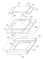
図1は、本発明の実施の形態1に係るEL光源体の主要構成の概要を説明する分解斜視図である。
FIG. 1 is an exploded perspective view for explaining the outline of the main configuration of the EL light source body according to
本実施の形態に係るEL光源体1は、光を放射する表面側に配置された表面ケース20、表面ケース20に対向して配置され光を発生するEL素子30、EL素子30へ電力の供給を行なう電極接続部40、表面ケース20に係合して光を放射する表面側と反対側の裏面を保護する裏面ケース50をこの順に位置合わせして重畳(嵌合、係合)することにより構成してある。
The EL
なお、表面ケース20、EL素子30、電極接続部40、裏面ケース50の相互間は、例えばエポキシ接着剤など適宜の接着剤を用いて安定的に固定することが可能であり、この構成によりEL光源体1の物理的強度を向上させ信頼性を向上させることができる。
The
表面ケース20は、EL素子30(透明基板32)に対向して配置されることから、EL光源体1の物理的強度を容易に確保することが可能となり、信頼性および実用性を向上させることができる。表面ケース20は、例えば、EL素子30を載置して支持する四辺形で平面状の支持部21と、支持部21の外周端に立設されてEL素子30(透明基板32)を内包し、位置決めして収容する枠部22とを備える。この構成により、EL素子30を表面ケース20の内側に確実に位置合わせして載置することができる。
Since the
表面ケース20は、EL素子30を安定的に支持して外部環境から確実に分離するので、EL素子30を周囲の外部環境から保護することが可能となる。したがって、EL光源体1の機械的強度を容易に確保することが可能となり、信頼性および実用性を向上させることができる。
Since the
表面ケース20により、例えばガラスで形成され外力に敏感な透明基板32のコーナ部(四辺形平面状での4つの角部、両平面と交差する端面での角部)の補強、保護が可能となるという効果を奏する。また、例えばガラスを切ることにより透明基板32に形成される四辺形端面でのシャープエッジの保護、被覆が可能となり、シャープエッジによる作業者の切り傷など作業上の困難性を排除し、取り扱い容易性を向上することにより、表面ケース20に実装した後の工程での作業性を向上することができるという効果を奏する。
The
支持部21の中央にはEL素子30からの光をEL光源体1の外部に直接放出(透過)するためにEL素子30の発光領域31に対応させて開口された窓部23が形成してある。つまり、支持部21は、EL素子30の外周部分に対応させて額縁状としてあることから、EL素子30の周囲を確実に支持することができる。したがって、発光領域31で発生した光はEL光源体1の外部へ直接放出されることから、窓部23を設けない場合に比較してEL光源体1としての光放出効率を向上させることが可能となり、透過率を低下させることなく物理的強度を確保することが可能となる。
In the center of the
表面ケース20は、例えば合成樹脂で成形してあり、窓部23を有することから遮光性樹脂で形成することが可能となる。表面ケース20を遮光性の合成樹脂(例えばプラスチック)で成形することによりEL素子30の発光領域31を際立たせて発光領域31を顕在化させ、また、発光領域31の周囲(外側領域)の非発光領域を見えないように遮光(マスキング)することが可能となることから、EL光源体1を照明用光源として用いる場合に透過率を低減させずに装飾性、デザイン性を向上させることができる。特に、第2極性接続部材42をマスキングできることから、視覚上大きな効果を奏する。
The
他方、表面ケース20を透光性とした場合には、窓部23を設けずに平板状とすることが可能になるという効果がある。
On the other hand, when the
EL素子30は製造の容易性などから一般的に四辺形とされるので、表面ケース20も同様に四辺形としてあるが、表面ケース20は、EL素子30の形状に応じて適宜変形することが可能である。
Since the
EL素子30は、光を放出する側(表面ケース20に対向する側)に配置された透明基板32、透明基板32の中央に構成される発光領域31を被覆し透明基板32と対向するように配置された封止部33を備える。透明基板32は、対向する支持部21に載置されることから、EL素子30としての物理的強度を向上することが可能となる。
The
また、透明基板32の裏面(封止部33に対向する側の面。光を外部に放出する面と反対側の面。)の外周領域には、封止部33の外周領域へ導出されたEL素子30の第1極性電極34p、第2極性電極34m(以下、第1極性電極34p、第2極性電極34mを区別する必要がない場合には、素子電極34という。例えば第1極性電極34pがプラス電極、第2極性電極34mがマイナス電極に対応する。)が配置、形成してある。
Further, the
第1極性電極34p、第2極性電極34mそれぞれは、例えば、透明基板32(封止部33)の外周領域の反対方向に同一極性の一対の電極として導出され配置されている。つまり、第1極性電極34p、第2極性電極34mは、互いに交差する方向に導出され、配置されている。
For example, each of the
なお、EL素子30については、図2でさらに詳細を説明する。
Details of the
電極接続部40は、封止部33に対向して配置され第1極性電極34p相互を接続する第1極性接続部材41と、透明基板32に対向して配置され第2極性電極34m相互を接続する第2極性接続部材42とを備える。図1では、第1極性接続部材41および第2極性接続部材42を模式的に示している。
The
相互に対向して配置された第1極性電極34pを封止部33に対向する側で接続し、第1極性電極34pに交差する方向で相互に対向して配置された第2極性電極34mを透明基板32に対向する側で接続することにより、EL素子30に電力を供給するための配線構造を簡略化して容易に形成することができる。
The
また、第1極性接続部材41および第2極性接続部材42を素子電極34に対応させた形状とすることにより、素子電極34の抵抗による電位差を確実に抑制して輝度斑を低減することが可能となり、高輝度で安定した動作が可能で物理的強度および信頼性の高いEL光源体1とすることが可能となる。
In addition, by forming the first
なお、電極接続部40については、実施の形態2ないし実施の形態5(図3ないし図9)でさらに詳細を説明する。
The
裏面ケース50は、EL素子30の外周部で電極接続部40が素子電極34と接続された領域を被覆する被覆部51、被覆部51の外周端に立設されてEL素子30を内包する枠部52を備える。つまり、裏面ケース50(枠部52)は、表面ケース20(枠部22)の内側に嵌合(係合)されて収容され、EL素子30を覆うように構成してあることから、表面ケース20と係合してEL素子30を外部環境から確実に分離して保護することが可能となり、EL光源体1の物理的強度をさらに向上させて、信頼性および実用性を向上させることができる。
The
したがって、EL素子30は、表面ケース20と裏面ケース50で構成される箱に収納され、いわゆるカセット構造のEL光源体1となるので、取り扱いが極めて容易となり、照明光源としての実用性を大きく向上させることが可能となる。
Accordingly, since the
被覆部51にはEL素子30からの熱をEL光源体1の外部に放出するために封止部33(第1極性接続部材41)に対応する領域を露出させる窓部53が形成してある。つまり、被覆部51は、EL素子30の外周部分に対応させて額縁状としてあることから、EL素子30で発生した熱はEL光源体1の外部へ直接放出される。
The covering
したがって、被覆部51は、窓部53を設けない場合に比較してEL光源体1としての放熱効率を向上させることから、放熱性を低下させることなく物理的強度を確保することが可能であり、また、窓部53から突出する形状の放熱体(不図示)を設けてさらに放熱性を向上させることも可能である。
Therefore, since the covering
裏面ケース50は、熱伝導性の高い素材で構成することも可能であり、この場合は、窓部53を設けずに、裏面ケース50を封止部33に当接(密着)させて放熱手段として用いることも可能である。この構成によれば、構成部品数を削減することが可能となり、製造工程の簡略化、製造コストの低減が可能になるという効果を奏する。
The
なお、表面ケース20と裏面ケース50で構成される箱(ケース)にEL素子30を収容した状態については、図10でさらに説明する。
The state in which the
また、EL光源体1を組み立てるときに、表面ケース20の支持部21にEL素子30の透明基板32を載置し、裏面ケース50を表面ケース20に嵌合してEL素子30を容易に箱に収容してEL光源体1とすることができるので極めて容易に製造することが可能となる。つまり、製造工程および完成後においてEL素子30に過剰な圧力が加わることがないので、製造歩留まり、信頼性を向上することができる。
When the EL
枠部22および枠部52のいずれか一方を省略して、表面ケース20および裏面ケース50のいずれか一方を平板状とし、他方に対して蓋状に配置して構成することも可能である。
One of the
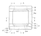
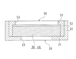
図2は、本発明の実施の形態1に係るEL光源体に適用されるEL素子の主要構成を説明する説明図であり、(A)は裏面側を示す平面図、(B)は(A)の矢符B−Bでの断面図、(C)は(A)の矢符C−Cでの断面図である。
2A and 2B are explanatory diagrams for explaining the main configuration of the EL element applied to the EL light source body according to
EL素子30は、相互に対向して配置された透明基板32および封止部33を備える。封止部33は、封止板33pと封着部33jで構成され、封着部33jを介して封止板33pを透明基板32に接合してある。透明基板32は発光領域31から光を外部へ導出するために透明性を要求され、例えばガラス基板で構成してある。封止板33pは、信頼性を確保するために耐湿性に優れる例えばガラス基板で構成してある。また、封着部33jは、ガラス基板を相互に接着するために例えばエポキシ系の接着剤を適用することが可能である。
The
透明基板32には、同図(A)で左右方向に第1極性電極34pが封止部33の外周領域へ導出して形成され、上下方向に第2極性電極34mが封止部33の外周領域へ導出して形成されている。つまり、透明基板32の電極接続部40に対向する面には封止板33pの周縁(辺)に沿って導出された素子電極34が延在配置してある(素子準備工程)。
In the
また、第1極性電極34pおよび第2極性電極34mは、発光領域31に対応する領域で発光層31eを挟むように積層して形成してある。なお、素子電極34の形状の関係から発光領域31が長方形に記載してあるが、素子電極34のパターン形状を適宜調整することにより、正方形にすることも可能である(以下、正方形で示すこともある。)。
The
なお、発光斑(輝度斑)を低減させるため、第1極性電極34pおよび第2極性電極34mを相互に交差する方向に両側から取り出す形状としてある。また、図示しないが、発光層31eを挟んでプラス側に正孔輸送層、マイナス側に電子輸送層が形成してある。発光層31eを有機分子で構成したものが有機EL発光素子である。
In addition, in order to reduce light emission spots (luminance spots), the
EL素子30は有機EL発光素子とすることにより、低電圧での点灯が可能で、発光効率の良いEL光源体とすることができる。なお、EL素子30の発光層31eおよび発光層31eに積層される正孔輸送層、電子輸送層などの構造については種々のものが提案されており、上述した構造に限るものではない。
When the
発光領域31で、透明基板32に積層され表面電極を構成する第1極性電極34pは、光を放出する必要があることから透明性を要求され、例えばITO(Indium Tin Oxide:酸化インジウム錫)で構成される。また、発光層31eに対して裏面側に積層され裏面電極を構成する第2極性電極34mは、透明性を要求されず適宜の反射性を要求されることから、例えばアルミニウムで構成される。なお、第1極性電極34pおよび第2極性電極34mの端部は上述したとおり、電極接続部40に対向する透明基板32の外周領域に導出される。
In the
透明基板32、封止板33pは、例えば10ないし20cm角のガラス基板であり、厚さは例えば1mmより薄く形成することが可能である。透明基板32の周縁(周縁領域/周縁部)は、封止板33p(封止部33)の辺に沿って素子電極34を導出して形成することから、上述したとおり透明基板32は封止板33pより大きく構成してある。
The
なお、理解を容易にするために素子電極34のレイアウト構成は単純な形態のものとしているがこれに限るものではなく、各辺でさらに分割した素子電極34としてあっても良い。
In order to facilitate understanding, the layout configuration of the
<実施の形態2>
本実施の形態は、EL素子と電極接続部との配置関係に関する。なお、実施の形態1と同様の構成については適宜説明を省略する。
<Embodiment 2>
The present embodiment relates to an arrangement relationship between the EL element and the electrode connection portion. Note that the description of the same configuration as that of
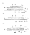
図3は、本発明の実施の形態2に係るEL光源体に適用されるEL素子と電極接続部(第1極性接続部材、第2極性接続部材)との配置関係を説明する分解斜視図である。図4および図5は、図3で示したEL素子と電極接続部を接続した状態での配置関係を説明する説明図であり、図4は裏面側を示す平面図、図5(A)は図4の矢符A−Aでの断面図、図5(B)は図4の矢符B−Bでの断面図、図5(C)は図4の矢符C−Cでの断面図である。 FIG. 3 is an exploded perspective view illustrating an arrangement relationship between an EL element applied to the EL light source body according to Embodiment 2 of the present invention and an electrode connection portion (first polarity connection member, second polarity connection member). is there. 4 and 5 are explanatory diagrams for explaining the arrangement relationship in a state where the EL element and the electrode connecting portion shown in FIG. 3 are connected. FIG. 4 is a plan view showing the back side, and FIG. 4 is a cross-sectional view taken along the arrow AA in FIG. 4, FIG. 5B is a cross-sectional view taken along the arrow BB in FIG. 4, and FIG. 5C is a cross-sectional view taken along the arrow C-C in FIG. It is.
電極接続部40は、上述したとおり第1極性接続部材41および第2極性接続部材42により構成される。第1極性接続部材41および第2極性接続部材42は、例えば板状導電体で構成してある。板状導電体としては、例えば銅板、アルミニウム板、42アロイ板、リン青銅板、導電性プラスチック板などを適用することができる。
The
第1極性接続部材41および第2極性接続部材42は、板状とされることからEL素子30の平面性を損なうことがなく、EL光源体1の薄型化を図ることが可能となる。また、板状であることから、物理的強度を確保してEL素子30の物理的強度を補強し、信頼性の高いEL光源体1とすることが可能となる。
Since the first
第1極性接続部材41は、封止部33の平面部に対向して配置される封止対向部41a、封止対向部41aの両端で封止部33の厚さに対応させて封止対向部41aに対して山折状に予め折り曲げてある厚み整合部41b、厚み整合部41bの先端に形成され厚み整合部41bに対して谷折状に予め折り曲げある接続端子部41cを有する。板状導電体を予め折り曲げて形成しておくことから、第1極性接続部材41を容易に準備することが可能となり、また、ガラス基板などで構成される封止部33への影響を避けることが可能となる。
The first
つまり、封止部33および第1極性電極34pに対向して沿うように形成された第1極性接続部材41は、封止部33および第1極性電極34pに対向して配置されることから、接続端子部41cと第1極性電極34pとを容易かつ確実に接続することが可能となる(第1極性接続工程)。つまり、第1極性電極34p相互の接続を生産性良く行なうことが可能となる。
That is, since the first
なお、第1極性接続部材41は、封止部33に対して矢符Setで示すように重畳するだけで良いことから、接続端子部41cと第1極性電極34pとを極めて容易に接続することができる。
Since the first
したがって、一対の第1極性電極34pは第1極性接続部材41によって相互に接続(短絡)され同電位にされることから、第1極性電極34pが有する抵抗による電位差を抑制することが可能となり、輝度斑を低減して輝度を向上させることが可能となる。また、接続端子部41cは、第1極性電極34pに対してほぼ全面に対応させて配置、接続することにより、第1極性電極34pの抵抗による電位差をさらに抑制して輝度斑を低減することが可能となる。
Therefore, since the pair of
また、板状導電体(第1極性接続部材41)で封止部33を覆うことから、EL素子30(EL光源体1)の物理的強度を向上させて信頼性の高いEL光源体1を生産性良く製造することが可能となる。
Further, since the sealing
特に、第1極性接続部材41を封止部33に密接させた状態で配置することにより、EL素子30の物理的強度および放熱性をさらに向上することが可能となる。封止対向部41aと封止部33とを接着剤で固定することにより、EL素子30の物理的強度および放熱性を補強することが可能となる。なお、第1極性接続部材41(封止対向部41a)には、放熱部を設けることが可能であり、放熱部を設けることによりさらに放熱性を向上させることができる。
In particular, the physical strength and heat dissipation of the
第2極性接続部材42は、透明基板32の平面部(光を放射する表面側)に対向して配置される基板対向部42a、基板対向部42aの両端で透明基板32の厚さに対応させて基板対向部42aに対して山折状に予め折り曲げてある厚み整合部42b、厚み整合部42bの先端に形成され厚み整合部42bに対して山折状に予め折り曲げある接続端子部42cを有する。
The second
基板対向部42aには、光を外部に放出するために発光領域31に対応させて透光用の窓部42dが形成してある。したがって、第2極性接続部材42(基板対向部42a)は、表面ケース20の窓部23を画定する支持部21と透明基板32との間に配置されることとなる。この構成により、第2極性接続部材42を発光領域31の周囲(外周領域)に配置し、また外部から保護することが可能となり、第2極性接続部材42の信頼性およびEL光源体1の透光性を確保することができる。また、板状導電体を予め折り曲げて形成しておくことから、第2極性接続部材42を容易に準備することが可能となる。
In the
つまり、透明基板32および第2極性電極34mに対向して沿うように形成された第2極性接続部材42(基板対向部42a)は透明基板32に対向して配置され、第2極性接続部材42(接続端子部42c)は第2極性電極34mに対向して配置されることから、接続端子部42cと第2極性電極34mとを容易かつ確実に接続することが可能となる(第2極性接続工程)。したがって、第2極性電極34m相互の接続を生産性良く行なうことが可能となる。
That is, the second polarity connection member 42 (
なお、接続端子部42cと第2極性電極34mとの接続は、第2極性接続部材42の厚さ方向に形成された溝部(両側を山折された厚み整合部42bで構成される溝部)に透明基板32を矢符Insで示すように嵌挿(差込)するだけで良いことから、極めて容易に行なうことができる。
In addition, the connection between the
したがって、一対の第2極性電極34mは第2極性接続部材42によって相互に接続(短絡)され同電位にされることから、第2極性電極34mが有する抵抗による電位差を抑制することが可能となり、輝度斑を低減して輝度を向上させることが可能となる。また、接続端子部42cは、第2極性電極34mに対してほぼ全面に対応させて配置、接続することにより、第2極性電極34mの抵抗による電位差をさらに抑制して輝度斑を低減することが可能となる。
Therefore, since the pair of
また、板状導電体(第2極性接続部材42)で透明基板32の外周領域(枠状領域)を覆うことから、EL素子30(EL光源体1)の物理的強度を向上させて信頼性の高いEL光源体1を生産性良く製造することが可能となる。特に、第2極性接続部材42(基板対向部42a)を透明基板32に密接させた状態で配置することにより、EL素子30の物理的強度をさらに向上することが可能となる。透明基板32と基板対向部42aとを接着剤で固定することにより、EL素子30の物理的強度を補強することが可能となる。
Further, since the outer peripheral area (frame area) of the
第1極性接続部材41と第1極性電極34pとの接続、第2極性接続部材42と第2極性電極34mとの接続は、例えば導電接着剤、導電性両面テープなど、適宜の手段を用いて行なうことができる。
The connection between the first
透明基板32と基板対向部42aとを接着剤で固定する代わりに適宜の圧力で接続端子部42cを基板対向部42aに対して押圧して圧接させることも可能である。あるいは、接続端子部42cに適宜のバネ性を持たせて第2極性電極34mに圧接する形態とすることも可能である。この場合は、第2極性接続部材42と第2極性電極34mとは、導電接着剤、導電性両面テープなどを用いなくても接続することが可能となる。両者を併用することも当然可能である。
Instead of fixing the
なお、第1極性接続工程および第2極性接続工程は、いずれを先に行なっても良い。 Note that either the first polarity connection step or the second polarity connection step may be performed first.
また、電極接続部40は、透明基板32に沿う薄い平面状の第2極性接続部材42および封止部33に沿う薄い平面状の第1極性接続部材41により構成され、封止部33の厚みにより形成される空間で素子電極34と接続されることから配線のための特別なスペースが不要であり、EL光源体1を薄型化することが可能となる(図3ないし図9参照)。
In addition, the
第1極性接続部材41の両端で接続端子部41cを素子電極34に接続して透明基板32を覆い、また、第1極性接続部材41と交差する方向に配置された第2極性接続部材42の両端で接続端子部42cを素子電極34に接続して透明基板32を表裏両面から覆うことにより、透明基板32の端部を表裏両面から覆う構成とすることが可能となり、透明基板32の端面の補強が可能となる。
The
また、第2極性接続部材42により、透明基板32のコーナ部を確実に覆うことが可能となることから、上述した透明基板32の補強、保護を更に向上させることが可能であり、シャープエッジの問題も併せて防止することが可能となる。
In addition, since the corner portion of the
また、適宜のリード端子(不図示)を第1極性接続部材41、第2極性接続部材42に接続して外部電源からコネクタ(不図示)を介してEL素子30に電力を供給することが可能である。第1極性接続部材41、第2極性接続部材42に接続したリード端子を導出する端子導出部を支持部21の1辺に対応する枠部22の中央付近に適宜形成することが可能である。
In addition, it is possible to connect an appropriate lead terminal (not shown) to the first
<実施の形態3>
本実施の形態は、実施の形態2として示したEL素子30と電極接続部40との配置関係の変形例に関する。なお、実施の形態2と同様の構成については適宜説明を省略する。
<Embodiment 3>
The present embodiment relates to a modification example of the arrangement relationship between the
図6は、本発明の実施の形態3に係るEL光源体に適用される電極接続部(第2極性接続部材)の変形例を示す工程断面図であり、(A)は第2極性接続部材を透明基板に当接して基板対向部を位置合わせした状態の断面図、(B)は第2極性接続部材を折り曲げて透明基板の側面に厚み整合部を形成した状態の断面図、(C)は第2極性接続部材をさらに折り曲げて第2極性電極に電極接続部を当接した状態の断面図である。なお、断面は図5(B)と同様の位置について示す。 FIG. 6 is a process cross-sectional view showing a modified example of the electrode connecting portion (second polarity connecting member) applied to the EL light source body according to Embodiment 3 of the present invention, and (A) shows the second polarity connecting member. Sectional view of the state where the substrate facing portion is aligned with the transparent substrate in contact with the transparent substrate, (B) is a sectional view of the state where the second polarity connecting member is bent to form the thickness matching portion on the side surface of the transparent substrate, (C) FIG. 5 is a cross-sectional view of a state where the second polarity connecting member is further bent and the electrode connecting portion is brought into contact with the second polarity electrode. Note that the cross section is shown at a position similar to that in FIG.
実施の形態2(図3ないし図5)で説明した第2極性接続部材42は、予め折り曲げられた状態のものを第2極性電極34mと接続する形態として説明したが、本実施の形態では、平板状態の第2極性接続部材42を透明基板32に当接した後に折り曲げて第2極性電極34mと接続する形態とする。
The second
図6(A)では、透明基板32に対して第2極性接続部材42(基板対向部42aおよび窓部42d)の位置合わせをした状態を示している。なお、実際の作業は、天地を逆にして行なうことにより、容易に位置合わせを行なうことができる。また、このとき、適宜の接着剤を適用して基板対向部42aと透明基板32とを接着することにより、第2極性接続部材42を安定的に固定することが可能となり、以降の折り曲げを高精度で容易にすることができる。また、透明基板32に対して第2極性接続部材42を固定することから、第2極性電極34mと第2極性接続部材42との接続の信頼性を向上させることが可能となる。
FIG. 6A shows a state in which the second polarity connection member 42 (the
図6(B)では、第2極性接続部材42を基板対向部42aに対して山折することにより、透明基板32の側面に対応する厚み整合部42bを形成する状態を示している。第2極性接続部材42は、板厚、硬さを適宜調整することにより容易に折り曲げすることが可能となる。図6(C)では、第2極性接続部材42を厚み整合部42bに対して山折することにより、第2極性電極34mに当接する接続端子部42cを形成した状態を示している。
FIG. 6B shows a state in which the
<実施の形態4>
本実施の形態は、実施の形態2、実施の形態3で示したEL素子30と電極接続部40との配置関係の変形例に関する。なお、実施の形態2、実施の形態3と同様の構成については適宜説明を省略する。
<Embodiment 4>
The present embodiment relates to a modification of the arrangement relationship between the
図7は、本発明の実施の形態4に係るEL光源体に適用される電極接続部(第2極性接続部材)の変形例を示す分解斜視図である。なお、第1極性接続部材41は、実施の形態2(図3)、実施の形態3(図6)で示した場合と同様に構成することが可能であり図示は省略してある。
FIG. 7 is an exploded perspective view showing a modification of the electrode connecting portion (second polarity connecting member) applied to the EL light source body according to Embodiment 4 of the present invention. The first
本実施の形態では、実施の形態2および実施の形態3で示した厚み整合部42b、接続端子部42cに代えて厚み整合部42e、接続端子部42fを設けている。厚み整合部42e、接続端子部42fは、厚み整合部42b、接続端子部42cに対して交差する方向で配置形成してある。つまり、第2極性電極34mの導出方向と交差する方向で、両側に厚み整合部42e、接続端子部42fがそれぞれ配置(計4箇所)してある。
In the present embodiment, a
厚み整合部42e、接続端子部42fは、厚み整合部42b、接続端子部42cに対して交差する方向で配置形成してあることから、図示した状態ではEL素子30を第2極性接続部材42に差し込む形態(実施の形態2)とすることはできない。したがって、実施の形態3で示したように、透明基板32に対して平板状態の第2極性接続部材42を位置合わせした後、第2極性接続部材42を折り曲げて図示した状態の厚み整合部42e、接続端子部42fとすることが必要となる。
Since the
つまり、本実施の形態では、透明基板32に対して平板状態の第2極性接続部材42を位置合わせした後、実施の形態3の場合と同様にして第2極性接続部材42を折り曲げて厚み整合部42e、接続端子部42fを形成する形態としてある。厚み整合部42e、接続端子部42fは、折り曲げ部分の幅を小さくできることから、実施の形態3(図6)の場合に比較して折り曲げ加工が容易になる。
That is, in the present embodiment, after aligning the flat second
<実施の形態5>
実施の形態2ないし実施の形態4では電極接続部40(第1極性接続部材41および第2極性接続部材42)を板状導電体としたが、本実施の形態では、電極接続部40を箔状導電体で構成してある。なお、実施の形態2ないし実施の形態4と同様の構成については適宜説明を省略する。
<Embodiment 5>
In the second to fourth embodiments, the electrode connecting portion 40 (the first
図8は、本発明の実施の形態5に係るEL光源体に適用されるEL素子と電極接続部(第1極性接続部材)との配置関係を示す工程断面図であり、(A)はEL素子と第1極性接続部材を位置合わせした状態を示す断面図、(B)はEL素子と第1極性接続部材を接着した状態を示す断面図、(C)はEL素子の素子電極と第1極性接続部材の接続端子部を接続した状態を示す断面図である。なお、断面は図5(A)と同様の位置について示し、箔状導電体の厚さを相対的に大きく図示している。 FIG. 8 is a process cross-sectional view showing an arrangement relationship between an EL element applied to an EL light source body according to Embodiment 5 of the present invention and an electrode connection portion (first polarity connection member), and FIG. Sectional drawing which shows the state which aligned the element and the 1st polarity connection member, (B) is sectional drawing which shows the state which adhere | attached the EL element and the 1st polarity connection member, (C) is the element electrode and 1st of EL element It is sectional drawing which shows the state which connected the connection terminal part of the polar connection member. Note that the cross section shows the same position as in FIG. 5A, and the thickness of the foil conductor is relatively large.
本実施の形態では、電極接続部40(第1極性接続部材43および第2極性接続部材45)を箔状導電体で構成してある。また、図8では、第2極性接続部材45の図示を省略してある。箔状導電体としては、例えば銅箔、アルミニウム箔、導電性プラスチック箔などを適用することができる。
In the present embodiment, the electrode connecting portion 40 (the first
図8(A)では、EL素子30の封止部33に対して接着剤45および第1極性接続部材43を位置合わせした状態を示している。
FIG. 8A shows a state where the adhesive 45 and the first
接着剤45は封止部33に接着(積層)されて第1極性接続部材43を接着するように封止部33および第1極性接続部材43に対応する形状としてある。第1極性接続部材43は、接着剤45を介して封止部33に接着される。接着剤45は、一般的な塗布形態の接着剤でも良いが、両面テープとすることが好ましい。この構成により第1極性接続部材43(箔状導電体)の平坦性を維持することが可能となり、また、第1極性接続部材43を容易かつ確実に固定することが可能となる。なお、接着剤45(両面テープ)は、熱伝導性の良い素材を適用することが好ましい。
The adhesive 45 has a shape corresponding to the sealing
第1極性接続部材43は、封止対向部43a、厚み整合部43b、接続端子部43cに対応する領域を有する平面状態で配置されている。つまり、第1極性接続部材43は、図3で示した第1極性接続部材41の折り曲げ前の形状と同様の平面状態で配置される。
The first
図8(B)では、EL素子30の封止部33に対して接着剤45および第1極性接続部材43を接着した状態を示している。接着剤45を適用することにより、箔状導電体で構成された第1極性接続部材43を容易かつ確実に封止部33に固定して配置することが可能となり、第1極性接続部材43の物理的強度を向上させて信頼性の高いEL光源体1とすることができる。
FIG. 8B shows a state where the adhesive 45 and the first
図8(C)では、EL素子30の第1極性電極34pと第1極性接続部材43の接続端子部43cを接続した状態を示している。第1極性接続部材43は、箔状導電体であることから、封止部33のエッジで封止部33の厚さに対応させて容易に折り曲げられ、厚み整合部43b、接続端子部43cを形成されている。
FIG. 8C shows a state where the
したがって、接続端子部43cと第1極性電極34pとを容易かつ確実に接続することが可能となる(第1極性接続工程)。なお、接続端子部43cと第1極性電極34pの接続は、他の実施の形態と同様に行なうことが可能である。つまり、第1極性電極34p相互の接続を生産性良く行なうことが可能となる。
Therefore, the connection terminal portion 43c and the
本実施の形態では、第1極性接続部材43を封止部33および第1極性電極34pに沿って容易に配置できることから平面性が良くさらに薄型のEL光源体1とすることが可能となり、また、第1極性接続部材43を容易かつ確実に第1極性電極34pに接続できることから生産性の高いEL光源体1とすることが可能となる。
In the present embodiment, since the first
図9は、本発明の実施の形態5に係るEL光源体に適用されるEL素子と電極接続部(第2極性接続部材)との配置関係を示す工程断面図であり、(A)はEL素子と第2極性接続部材を位置合わせした状態を示す断面図、(B)はEL素子と第2極性接続部材を接着した状態を示す断面図、(C)はEL素子の素子電極と第2極性接続部材の接続端子部を接続した状態を示す断面図である。なお、断面は図5(B)と同様の位置について示し、箔状導電体の厚さを相対的に大きく図示している。 FIG. 9 is a process cross-sectional view illustrating an arrangement relationship between an EL element applied to an EL light source body according to Embodiment 5 of the present invention and an electrode connection portion (second polarity connection member), and FIG. Sectional drawing which shows the state which aligned the element and the 2nd polarity connection member, (B) is sectional drawing which shows the state which adhere | attached the EL element and the 2nd polarity connection member, (C) is the element electrode and 2nd of EL element It is sectional drawing which shows the state which connected the connection terminal part of the polar connection member. Note that the cross section shows the same position as in FIG. 5B, and the thickness of the foil conductor is relatively large.
基本構成は図8に示した第1極性接続部材43と同様であるので、適宜説明を省略する。また、図9では、第1極性接続部材43の図示を省略してある。
The basic configuration is the same as that of the first
図9(A)では、EL素子30の透明基板32に対して接着剤46および第2極性接続部材44を位置合わせした状態を示している。
FIG. 9A shows a state in which the adhesive 46 and the second
接着剤46は透明基板32に接着(積層)されて第2極性接続部材44を接着するように透明基板32および第2極性接続部材44に対応する形状としてある。第2極性接続部材44は、接着剤46を介して透明基板32に接着される。接着剤46は、接着剤45と同様に構成することができる。なお、窓部42d(図3参照。)と同様に予め透光用の窓部44d(第2極性接続部材44)、窓部46d(接着剤46)が形成してある。また、実際の作業は、天地を逆にして行なうことにより、容易に位置合わせを行なうことができる。
The adhesive 46 has a shape corresponding to the
第2極性接続部材44は、基板対向部44a、厚み整合部44b、接続端子部44cに対応する領域を有する平面状態で配置されている。つまり、第2極性接続部材44は、図6で示した第2極性接続部材42の折り曲げ前の形状と同様の平面状態で配置される。
The second
図9(B)では、EL素子30の透明基板32に対して接着剤46および第2極性接続部材44を接着した状態を示している。接着剤46を適用することにより、箔状導電体で構成された第2極性接続部材44を容易かつ確実に透明基板32に固定して配置することが可能となり、第2極性接続部材44の物理的強度を向上させて信頼性の高いEL光源体1とすることができる。
FIG. 9B shows a state where the adhesive 46 and the second
図9(C)では、EL素子30の第2極性電極34mと第2極性接続部材44の接続端子部44cを接続した状態を示している。第2極性接続部材44は、箔状導電体であることから、透明基板32のエッジで透明基板32の厚さに対応させて容易に折り曲げられ、厚み整合部44b、接続端子部44cを形成されている。
FIG. 9C shows a state where the
したがって、接続端子部44cと第2極性電極34mとを容易かつ確実に接続することが可能となる(第2極性接続工程)。なお、接続端子部44cと第2極性電極34mの接続は、他の実施の形態と同様に行なうことが可能である。つまり、第2極性電極34m相互の接続を生産性良く行なうことが可能となる。
Therefore, the connection terminal portion 44c and the
本実施の形態では、第2極性接続部材44を透明基板32および第2極性電極34mに沿って容易に配置できることから平面性が良くさらに薄型のEL光源体1とすることが可能となり、また、第2極性接続部材44を容易に第2極性電極34mに接続できることから生産性の高いEL光源体1とすることが可能となる。
In the present embodiment, since the second
なお、他の実施の形態と同様、第1極性接続工程と第2極性接続工程は、いずれを先に行なっても良い。 As in the other embodiments, either the first polarity connection step or the second polarity connection step may be performed first.
<実施の形態6>
実施の形態1で記載した表面ケース20および裏面ケース50は、実施の形態2ないし実施の形態5に係るEL素子30についてもそのまま適用することが可能である。本実施の形態では、実施の形態1ないし実施の形態5に示したEL素子30を表面ケース20および裏面ケース50により収納した状態のEL光源体1を説明する。
<Embodiment 6>
The
図10は、本発明の実施の形態1ないし実施の形態5に係るEL光源体の外形(表面ケースおよび裏面ケース)を説明する断面図である。なお、図では、簡単のためにEL素子30および電極接続部40を一体として示している。基本的な構成は図1と同様であるので詳細な説明は省略する。
FIG. 10 is a cross-sectional view illustrating the outer shape (front case and back case) of the EL light source body according to
表面ケース20の支持部21に形成された窓部23に対応させて発光領域31(図10では図示しない。)が配置され、枠部22にEL素子30および電極接続部40が収容されている。EL素子30および電極接続部40は、裏面ケース50の内周に係合されている。また、表面ケース20および裏面ケース50は相互に係合してEL素子30および電極接続部40を保護する形態としてある。
A light emitting region 31 (not shown in FIG. 10) is arranged corresponding to the
<実施の形態7>
本実施の形態は、実施の形態6で示した表面ケース20および裏面ケース50を一体化してスライドケースとしたEL光源体に関する。実施の形態6と同様の構成については適宜説明を省略する。
<Embodiment 7>
The present embodiment relates to an EL light source body in which the
図11は、本発明の実施の形態7に係るEL光源体の外形(スライドケース)を説明する斜視図である。基本的には実施の形態1で示した表面ケース20および裏面ケース50と同様に機能するので適宜説明を省略する。
FIG. 11 is a perspective view for explaining the outer shape (slide case) of the EL light source body according to Embodiment 7 of the present invention. Basically, it functions in the same manner as the
本実施の形態で示すスライドケース60は、発光領域31(図1参照。)に対応する表面板61、封止部33に対応する裏面板62、表面板61および裏面板62を3方向で連結する側板63を主要構成とする。側板63が存在しない1方向に開口部64が形成してある。表面板61および裏面板62は、それぞれ表面ケース20および裏面ケース50に対応し、同様に機能する。
The
表面板61には、発光領域31に対応させて窓部65が形成してある。また、裏面板62には、封止部33(図1参照。)に対応させて窓部66が形成してある。窓部65および窓部66は、窓部23および窓部53に対応し、同様に機能する。
A
本実施の形態では、一体化されたEL素子30および電極接続部40を開口部64からスライドケース60に対して矢符Insで示すようにスライド式に挿入する点が実施の形態1の場合と異なる。つまり、本実施の形態にかかるEL光源体1は、一体化されたEL素子30および電極接続部40を開口部64にスライド式に挿入することにより構成してある。したがって、表面ケース20および裏面ケース50を係合(嵌合)させる必要がなく、容易にEL光源体1を組み立てることが可能となる。
In the present embodiment, the point where the
また、第1極性接続部材41、第2極性接続部材42(図1参照。)に接続した適宜のリード端子(不図示)を開口部64から導出し、外部電源からコネクタ(不図示)を介してEL素子30に電力を供給することが可能である。
Also, appropriate lead terminals (not shown) connected to the first
1 EL光源体
20 表面ケース
21 支持部
22 枠部
23 窓部
30 EL素子
31 発光領域
31e 発光層
32 透明基板
33 封止部
33p 封止板
33j 封着部
34 素子電極
34p プラス電極
34m マイナス電極
40 電極接続部
41 第1極性接続部材
42 第2極性接続部材
43 第1極性接続部材
44 第2極性接続部材
45 接着剤
46 接着剤
50 裏面ケース
51 被覆部
52 枠部
53 窓部
60 スライドケース
65 窓部
66 窓部
DESCRIPTION OF
Claims (3)
前記封止部に沿うように配置されて一対の前記第1極性電極相互を接続する第1極性接続部材と、
前記透明基板の表面側を介して一対の前記第2極性電極相互を接続する第2極性接続部材と、
前記透明基板の表面に対向して配置され前記発光領域に対応する窓部を有する表面ケースと、
前記表面ケースに係合して前記EL素子を被う裏面ケースとを備え、
前記表面ケースは、遮光性を有し、前記裏面ケースは、前記封止部に対応する領域を露出する窓部を有することを特徴とするEL光源体。 A quadrilateral transparent substrate, a sealing portion that covers a light emitting region configured in the center of the transparent substrate and is disposed to face the back surface of the transparent substrate, and a first direction in plan view with respect to the sealing portion And a pair of first polarity electrodes that are derived from the sealing portion and disposed in the outer peripheral region of the back surface of the transparent substrate , and are derived from the sealing portion in a second direction that intersects the first direction in the plan view. An EL light source body comprising an EL element having a pair of second polar electrodes arranged in an outer peripheral region of the back surface of the transparent substrate,
A first polarity connection member arranged along the sealing portion to connect the pair of first polarity electrodes;
A second polarity connection member for connecting the pair of second polarity electrodes to each other via the surface side of the transparent substrate ;
A surface case disposed opposite to the surface of the transparent substrate and having a window corresponding to the light emitting region;
A back case that engages with the front case and covers the EL element;
The EL light source body , wherein the front case has light shielding properties, and the back case has a window portion that exposes a region corresponding to the sealing portion .
前記第1極性接続部材および前記第2極性接続部材は、板状導電体で形成してあり、前記第2極性接続部材は、前記透明基板に接着してあることを特徴とするEL光源体。 The EL light source body according to claim 1,
The EL light source body, wherein the first polarity connection member and the second polarity connection member are formed of a plate-like conductor, and the second polarity connection member is bonded to the transparent substrate.
前記第1極性接続部材および前記第2極性接続部材は、箔状導電体で形成してあり、前記第1極性接続部材は接着剤で前記封止部に接着され、前記第2極性接続部材は接着剤で前記透明基板に接着してあることを特徴とするEL光源体。 The EL light source body according to claim 1,
The first polarity connection member and the second polarity connection member are formed of a foil-like conductor, the first polarity connection member is bonded to the sealing portion with an adhesive, and the second polarity connection member is An EL light source body, which is bonded to the transparent substrate with an adhesive.
Priority Applications (1)
| Application Number | Priority Date | Filing Date | Title |
|---|---|---|---|
| JP2006109974A JP4868922B2 (en) | 2006-04-12 | 2006-04-12 | EL light source |
Applications Claiming Priority (1)
| Application Number | Priority Date | Filing Date | Title |
|---|---|---|---|
| JP2006109974A JP4868922B2 (en) | 2006-04-12 | 2006-04-12 | EL light source |
Publications (3)
| Publication Number | Publication Date |
|---|---|
| JP2007287344A JP2007287344A (en) | 2007-11-01 |
| JP2007287344A5 JP2007287344A5 (en) | 2009-05-07 |
| JP4868922B2 true JP4868922B2 (en) | 2012-02-01 |
Family
ID=38758952
Family Applications (1)
| Application Number | Title | Priority Date | Filing Date |
|---|---|---|---|
| JP2006109974A Expired - Fee Related JP4868922B2 (en) | 2006-04-12 | 2006-04-12 | EL light source |
Country Status (1)
| Country | Link |
|---|---|
| JP (1) | JP4868922B2 (en) |
Families Citing this family (3)
| Publication number | Priority date | Publication date | Assignee | Title |
|---|---|---|---|---|
| JP5264608B2 (en) * | 2009-04-23 | 2013-08-14 | パナソニック株式会社 | Organic EL panel for lighting |
| JP2013219184A (en) * | 2012-04-09 | 2013-10-24 | Sumitomo Chemical Co Ltd | Lighting panel and lighting device provided with the same |
| WO2013179482A1 (en) * | 2012-06-01 | 2013-12-05 | パイオニア株式会社 | Organic el light-emitting element and method for manufacturing same |
Family Cites Families (4)
| Publication number | Priority date | Publication date | Assignee | Title |
|---|---|---|---|---|
| JP2001085158A (en) * | 1999-09-10 | 2001-03-30 | Toyota Central Res & Dev Lab Inc | Organic electroluminescent element |
| TW465122B (en) * | 1999-12-15 | 2001-11-21 | Semiconductor Energy Lab | Light-emitting device |
| JP2004226507A (en) * | 2003-01-21 | 2004-08-12 | Nippon Seiki Co Ltd | Device for driving organic el panel |
| JP2005258097A (en) * | 2004-03-12 | 2005-09-22 | Citizen Watch Co Ltd | Panel connected with wiring member and method for manufacturing same |
-
2006
- 2006-04-12 JP JP2006109974A patent/JP4868922B2/en not_active Expired - Fee Related
Also Published As
| Publication number | Publication date |
|---|---|
| JP2007287344A (en) | 2007-11-01 |
Similar Documents
| Publication | Publication Date | Title |
|---|---|---|
| JP4860530B2 (en) | EL light source | |
| JP2007280693A (en) | El light source | |
| CN106449697B (en) | Display device and method for manufacturing the same | |
| JP5381447B2 (en) | Electro-optic device | |
| US9851076B2 (en) | Light-emitting device and mobile object | |
| JP5407649B2 (en) | ELECTRO-OPTICAL DEVICE, ITS MANUFACTURING METHOD, AND ELECTRONIC DEVICE | |
| JP2016110858A (en) | Planar light emission module | |
| JP4868922B2 (en) | EL light source | |
| JP6121092B2 (en) | Organic electroluminescence panel and manufacturing method thereof | |
| JP5407648B2 (en) | Electro-optical device manufacturing method, electro-optical device, and electronic apparatus | |
| JP2005078906A (en) | Organic electroluminescence panel | |
| JP2011044375A (en) | Electro-optical device, method for manufacturing electro-optical device, electronic equipment | |
| WO2016136577A1 (en) | Planar light-emitting module | |
| JP2002008856A (en) | Organic el panel | |
| JP2007287345A (en) | El light emitting module | |
| JP2022518790A (en) | Display device | |
| WO2015186487A1 (en) | Surface light emitting device and method for manufacturing same | |
| WO2014091761A1 (en) | Surface emitting light source and surface emitting light source assembly | |
| JP3938805B2 (en) | EL emission mark | |
| JP2008277047A (en) | Surface light source device and liquid crystal display device | |
| JP2005071944A (en) | Organic electroluminescent display device | |
| CN113192426B (en) | Display panel, display module and electronic equipment | |
| JP7441987B2 (en) | light emitting device | |
| JP6101458B2 (en) | Organic EL module and laying structure of organic EL module | |
| JP2014017204A (en) | Organic electroluminescent element and planar light-emitting unit |
Legal Events
| Date | Code | Title | Description |
|---|---|---|---|
| A521 | Request for written amendment filed |
Free format text: JAPANESE INTERMEDIATE CODE: A523 Effective date: 20090319 |
|
| A621 | Written request for application examination |
Free format text: JAPANESE INTERMEDIATE CODE: A621 Effective date: 20090319 |
|
| RD02 | Notification of acceptance of power of attorney |
Free format text: JAPANESE INTERMEDIATE CODE: A7422 Effective date: 20090319 |
|
| A977 | Report on retrieval |
Free format text: JAPANESE INTERMEDIATE CODE: A971007 Effective date: 20110308 |
|
| A131 | Notification of reasons for refusal |
Free format text: JAPANESE INTERMEDIATE CODE: A131 Effective date: 20110531 |
|
| A521 | Request for written amendment filed |
Free format text: JAPANESE INTERMEDIATE CODE: A523 Effective date: 20110708 |
|
| TRDD | Decision of grant or rejection written | ||
| A01 | Written decision to grant a patent or to grant a registration (utility model) |
Free format text: JAPANESE INTERMEDIATE CODE: A01 Effective date: 20111108 |
|
| A01 | Written decision to grant a patent or to grant a registration (utility model) |
Free format text: JAPANESE INTERMEDIATE CODE: A01 |
|
| A61 | First payment of annual fees (during grant procedure) |
Free format text: JAPANESE INTERMEDIATE CODE: A61 Effective date: 20111115 |
|
| R150 | Certificate of patent or registration of utility model |
Ref document number: 4868922 Country of ref document: JP Free format text: JAPANESE INTERMEDIATE CODE: R150 Free format text: JAPANESE INTERMEDIATE CODE: R150 |
|
| FPAY | Renewal fee payment (event date is renewal date of database) |
Free format text: PAYMENT UNTIL: 20141125 Year of fee payment: 3 |
|
| R250 | Receipt of annual fees |
Free format text: JAPANESE INTERMEDIATE CODE: R250 |
|
| R250 | Receipt of annual fees |
Free format text: JAPANESE INTERMEDIATE CODE: R250 |
|
| LAPS | Cancellation because of no payment of annual fees |