JP4864546B2 - Organic EL display device and manufacturing method thereof - Google Patents
Organic EL display device and manufacturing method thereof Download PDFInfo
- Publication number
- JP4864546B2 JP4864546B2 JP2006148415A JP2006148415A JP4864546B2 JP 4864546 B2 JP4864546 B2 JP 4864546B2 JP 2006148415 A JP2006148415 A JP 2006148415A JP 2006148415 A JP2006148415 A JP 2006148415A JP 4864546 B2 JP4864546 B2 JP 4864546B2
- Authority
- JP
- Japan
- Prior art keywords
- organic
- film
- transparent conductive
- conductive film
- reflective metal
- Prior art date
- Legal status (The legal status is an assumption and is not a legal conclusion. Google has not performed a legal analysis and makes no representation as to the accuracy of the status listed.)
- Expired - Fee Related
Links
- 238000004519 manufacturing process Methods 0.000 title claims description 15
- 239000010408 film Substances 0.000 claims description 206
- 229910052751 metal Inorganic materials 0.000 claims description 60
- 239000002184 metal Substances 0.000 claims description 60
- 239000000758 substrate Substances 0.000 claims description 27
- 239000011347 resin Substances 0.000 claims description 26
- 229920005989 resin Polymers 0.000 claims description 26
- 238000000034 method Methods 0.000 claims description 22
- 239000010409 thin film Substances 0.000 claims description 17
- 238000000926 separation method Methods 0.000 claims description 13
- 239000000463 material Substances 0.000 claims description 9
- 239000012528 membrane Substances 0.000 claims description 7
- 229910052782 aluminium Inorganic materials 0.000 claims description 5
- XAGFODPZIPBFFR-UHFFFAOYSA-N aluminium Chemical compound [Al] XAGFODPZIPBFFR-UHFFFAOYSA-N 0.000 claims description 5
- 229910045601 alloy Inorganic materials 0.000 claims description 4
- 239000000956 alloy Substances 0.000 claims description 4
- 229910052709 silver Inorganic materials 0.000 claims description 4
- 239000004332 silver Substances 0.000 claims description 4
- 238000005401 electroluminescence Methods 0.000 description 86
- 239000010410 layer Substances 0.000 description 53
- 239000011229 interlayer Substances 0.000 description 12
- 239000007789 gas Substances 0.000 description 7
- 239000011521 glass Substances 0.000 description 7
- 239000011159 matrix material Substances 0.000 description 7
- 229910052581 Si3N4 Inorganic materials 0.000 description 6
- 238000005530 etching Methods 0.000 description 6
- 239000004973 liquid crystal related substance Substances 0.000 description 6
- HQVNEWCFYHHQES-UHFFFAOYSA-N silicon nitride Chemical compound N12[Si]34N5[Si]62N3[Si]51N64 HQVNEWCFYHHQES-UHFFFAOYSA-N 0.000 description 6
- 230000005525 hole transport Effects 0.000 description 5
- 230000002093 peripheral effect Effects 0.000 description 5
- VYPSYNLAJGMNEJ-UHFFFAOYSA-N Silicium dioxide Chemical compound O=[Si]=O VYPSYNLAJGMNEJ-UHFFFAOYSA-N 0.000 description 4
- 238000000605 extraction Methods 0.000 description 4
- 230000007774 longterm Effects 0.000 description 4
- 229910021420 polycrystalline silicon Inorganic materials 0.000 description 4
- 229920005591 polysilicon Polymers 0.000 description 4
- 229910052814 silicon oxide Inorganic materials 0.000 description 4
- QTBSBXVTEAMEQO-UHFFFAOYSA-N Acetic acid Chemical compound CC(O)=O QTBSBXVTEAMEQO-UHFFFAOYSA-N 0.000 description 3
- 229920000178 Acrylic resin Polymers 0.000 description 3
- 239000004925 Acrylic resin Substances 0.000 description 3
- 229920001721 polyimide Polymers 0.000 description 3
- 239000009719 polyimide resin Substances 0.000 description 3
- 238000004544 sputter deposition Methods 0.000 description 3
- CBENFWSGALASAD-UHFFFAOYSA-N Ozone Chemical compound [O-][O+]=O CBENFWSGALASAD-UHFFFAOYSA-N 0.000 description 2
- 238000004140 cleaning Methods 0.000 description 2
- 230000007423 decrease Effects 0.000 description 2
- 230000000694 effects Effects 0.000 description 2
- 230000020169 heat generation Effects 0.000 description 2
- 230000004048 modification Effects 0.000 description 2
- 238000012986 modification Methods 0.000 description 2
- 230000003287 optical effect Effects 0.000 description 2
- 239000011368 organic material Substances 0.000 description 2
- 238000000206 photolithography Methods 0.000 description 2
- 238000002310 reflectometry Methods 0.000 description 2
- 239000000243 solution Substances 0.000 description 2
- XLYOFNOQVPJJNP-UHFFFAOYSA-N water Substances O XLYOFNOQVPJJNP-UHFFFAOYSA-N 0.000 description 2
- XLOMVQKBTHCTTD-UHFFFAOYSA-N zinc oxide Inorganic materials [Zn]=O XLOMVQKBTHCTTD-UHFFFAOYSA-N 0.000 description 2
- 239000011787 zinc oxide Substances 0.000 description 2
- 229910000838 Al alloy Inorganic materials 0.000 description 1
- 208000005156 Dehydration Diseases 0.000 description 1
- 238000010521 absorption reaction Methods 0.000 description 1
- 239000000654 additive Substances 0.000 description 1
- 230000000996 additive effect Effects 0.000 description 1
- 230000015572 biosynthetic process Effects 0.000 description 1
- 230000009920 chelation Effects 0.000 description 1
- 238000005229 chemical vapour deposition Methods 0.000 description 1
- 230000003749 cleanliness Effects 0.000 description 1
- 239000006059 cover glass Substances 0.000 description 1
- 230000002950 deficient Effects 0.000 description 1
- 230000018044 dehydration Effects 0.000 description 1
- 238000006297 dehydration reaction Methods 0.000 description 1
- 239000003822 epoxy resin Substances 0.000 description 1
- PCHJSUWPFVWCPO-UHFFFAOYSA-N gold Chemical compound [Au] PCHJSUWPFVWCPO-UHFFFAOYSA-N 0.000 description 1
- 229910052737 gold Inorganic materials 0.000 description 1
- 239000010931 gold Substances 0.000 description 1
- AMGQUBHHOARCQH-UHFFFAOYSA-N indium;oxotin Chemical compound [In].[Sn]=O AMGQUBHHOARCQH-UHFFFAOYSA-N 0.000 description 1
- 239000011261 inert gas Substances 0.000 description 1
- 238000002347 injection Methods 0.000 description 1
- 239000007924 injection Substances 0.000 description 1
- 239000000203 mixture Substances 0.000 description 1
- 229920000647 polyepoxide Polymers 0.000 description 1
- 239000011241 protective layer Substances 0.000 description 1
- 239000003566 sealing material Substances 0.000 description 1
- 239000004065 semiconductor Substances 0.000 description 1
- 239000002356 single layer Substances 0.000 description 1
- 238000009751 slip forming Methods 0.000 description 1
- 238000003860 storage Methods 0.000 description 1
- 238000001771 vacuum deposition Methods 0.000 description 1
- YVTHLONGBIQYBO-UHFFFAOYSA-N zinc indium(3+) oxygen(2-) Chemical compound [O--].[Zn++].[In+3] YVTHLONGBIQYBO-UHFFFAOYSA-N 0.000 description 1
Images


Landscapes
- Devices For Indicating Variable Information By Combining Individual Elements (AREA)
- Electroluminescent Light Sources (AREA)
Description
本発明は、有機EL(Electro Luminescence)表示装置およびその製造方法に関するものである。 The present invention relates to an organic EL (Electro Luminescence) display device and a manufacturing method thereof.
有機EL素子は、陽極電極(以下「アノード電極」という。)と陰極電極(以下「カソード電極」という。)との間に有機材料からなる正孔輸送層や発光層、電子注入層を積層させた構造を備えており、低電圧直流電流を印加することで発光する。有機EL素子は、直流電流印加から発光までの応答速度が速いので動画表示に優れる。また、有機EL素子は自発光素子であるため、液晶表示素子の場合のような補助光源が不要であり、薄型表示装置に適しているという点で注目されている。 In an organic EL element, a hole transport layer, a light emitting layer, and an electron injection layer made of an organic material are laminated between an anode electrode (hereinafter referred to as “anode electrode”) and a cathode electrode (hereinafter referred to as “cathode electrode”). It emits light when a low voltage direct current is applied. The organic EL element is excellent in moving image display because of its high response speed from application of direct current to light emission. Further, since the organic EL element is a self-luminous element, an auxiliary light source as in the case of a liquid crystal display element is unnecessary, and attention is paid in that it is suitable for a thin display device.
有機EL素子を用いた有機EL表示装置は、低電圧直流を印加・駆動するための方式によって、パッシブマトリックス駆動型と各画素にスイッチ素子を備えたアクティブマトリックス駆動型とに区別される。さらに、有機EL素子からの発光を取り出す向きによって区別され、有機EL素子が積層されている基板の側へ取り出すボトムエミッション型と、積層されている基板とは逆向きに取り出すトップエミッション型とに分けられる。 Organic EL display devices using organic EL elements are classified into a passive matrix drive type and an active matrix drive type in which each pixel is provided with a switch element according to a method for applying and driving a low voltage direct current. Furthermore, it is distinguished according to the direction in which the light emission from the organic EL element is extracted, and is divided into a bottom emission type in which the organic EL element is taken out to the side of the substrate on which the organic EL element is laminated and a top emission type in which the laminated substrate is taken away from It is done.
アクティブマトリックス駆動型でトップエミッション型の有機EL表示装置の例が特開2005−285395号公報(特許文献1)、特開2005−322564号公報(特許文献2)に開示されている。 Examples of an active matrix drive type top emission type organic EL display device are disclosed in Japanese Patent Application Laid-Open No. 2005-285395 (Patent Document 1) and Japanese Patent Application Laid-Open No. 2005-322564 (Patent Document 2).
特許文献1では、層間絶縁膜のコンタクトホール以外の部分の上面を覆うように反射板がAl系金属で形成され、ITOからなる膜厚100nmの陽極が反射板の上側を被覆している。TFTのドレイン電極からの低電圧直流電流はこの透明な陽極を介して有機EL層に印加される。
特許文献1に開示されている有機EL表示装置では、光の取出し効率を向上させて明るい有機EL表示装置を得るためには、光学設計上、「陽極」と称されているITO膜の膜厚を薄くし、かつ特定の膜厚にすることが望ましい。しかし、このITO膜が薄くなると、抵抗値が増大してしまう。また、コンタクトホールまたは反射板の段差部でのITO膜による被覆性が低下する。その結果、抵抗値増大や断線によって発光不良、非発光になる。そこで、ITO膜の膜厚を薄くし、なおかつ、被覆性の低下を補うためにAl系金属からなる反射板も薄くした場合、反射板による反射率が低下し、光の取出し効率が悪化してしまう。
In the organic EL display device disclosed in
特許文献2に開示されている有機EL表示装置では、アノード電極の役割を果たす「下部電極」がITO−Ag−ITOの3層構造となっている。ここではAg膜が反射膜の役割を果たしていると考えられ、Ag膜であれば高反射率であり透明導電膜としてのITO膜との接触抵抗も低く抑えられている。しかし、このような構造の場合、透明導電膜と反射膜との間に低抵抗の電気的接続が必要であり、反射金属膜、透明導電膜の材質が制限される。
In the organic EL display device disclosed in
また、本発明者らは、金属膜と有機樹脂とが接触し、かつ熱が加わることで水分およびガスの放出量が増大することを見出した。一方、有機EL層は水分に弱い。有機EL表示装置内に金属膜と有機樹脂膜との接触構造が含まれている場合、長期駆動による発熱または、炎天下などの高温使用環境により、有機EL表示装置内に水分、ガスが生じて有機EL層が劣化する。 Further, the present inventors have found that the amount of moisture and gas released increases when the metal film and the organic resin come into contact with each other and heat is applied. On the other hand, the organic EL layer is vulnerable to moisture. If the contact structure between the metal film and the organic resin film is included in the organic EL display device, moisture or gas is generated in the organic EL display device due to heat generated by long-term driving or high-temperature use environment such as under the sun. The EL layer deteriorates.
特許文献1の構造では金属からなる「反射板50」と有機樹脂からなる「層間絶縁膜36」とが接触している。特許文献2の構造では「下部電極15」に含まれるAg膜の側面が有機樹脂からなる「絶縁膜16」と接触している。したがって、特許文献1,2のいずれにおいても、長期駆動による発熱または、炎天下などの高温使用環境により水分、ガスが生じて有機EL層が劣化する。
In the structure of
そこで、本発明は、高信頼性、長寿命の有機EL表示装置を提供することを目的とする。 Therefore, an object of the present invention is to provide an organic EL display device with high reliability and long life.
上記目的を達成するため、本発明に基づく有機EL表示装置は、基板と、上記基板の主表面に形成された複数の薄膜トランジスタと、上記複数の薄膜トランジスタの上側を覆い、有機樹脂からなる平坦化膜と、上記平坦化膜の上側に配置され、上記複数の薄膜トランジスタの各々に電気的に接続された複数のアノード電極と、上記複数のアノード電極を個別に絶縁隔離するように形成され、有機樹脂からなる分離膜と、上記アノード電極に電気的に接続するように上記アノード電極の上側に配置された有機EL層と、上記有機EL層に電気的に接続するように上記有機EL層の上側に配置されたカソード電極とを備え、上記アノード電極は上記基板に近い側から順に、下部透明導電膜、反射金属膜、上部透明導電膜の3層を含み、上記反射金属膜は上面、下面および側面のすべてが透明導電膜で被覆されている。 In order to achieve the above object, an organic EL display device according to the present invention includes a substrate, a plurality of thin film transistors formed on the main surface of the substrate, and a planarizing film made of an organic resin that covers the upper sides of the plurality of thin film transistors. And a plurality of anode electrodes disposed on the planarizing film and electrically connected to each of the plurality of thin film transistors, and the plurality of anode electrodes are individually insulated and isolated from an organic resin. An organic EL layer disposed above the anode electrode so as to be electrically connected to the anode electrode, and disposed above the organic EL layer so as to be electrically connected to the organic EL layer. The anode electrode includes three layers of a lower transparent conductive film, a reflective metal film, and an upper transparent conductive film in order from the side close to the substrate, and the reflective gold Film top surface, all of the lower surface and side surfaces are coated with a transparent conductive film.
本発明によれば、反射金属膜の上面、下面、側面のすべてが透明導電膜により被覆され、その結果、金属膜と有機樹脂からなる膜とが直接接触する箇所がない構成となっているので、内部での水分およびガスの発生を低減することができ、高信頼性、長寿命の有機EL表示装置を実現することができる。 According to the present invention, the upper surface, the lower surface, and the side surface of the reflective metal film are all covered with the transparent conductive film, and as a result, there is no place where the metal film and the film made of organic resin are in direct contact. The generation of moisture and gas inside can be reduced, and a highly reliable and long-life organic EL display device can be realized.
発明者らは、有機EL表示装置に用いられる有機EL層の長寿命化のために鋭意研究を重ねた結果、金属膜と有機樹脂膜とが接触している状態に比べて、透明導電膜と有機樹脂膜とが接触している状態の方が、水分およびガスの放出量が大幅に少なく、有機EL層の寿命が延びることを見出した。この知見に基づいて、以下の発明はなされた。 As a result of intensive studies for extending the lifetime of the organic EL layer used in the organic EL display device, the inventors have compared the transparent conductive film with the metal film and the organic resin film being in contact with each other. It has been found that when the organic resin film is in contact with the organic resin film, the amount of moisture and gas released is significantly less, and the life of the organic EL layer is extended. Based on this knowledge, the following invention was made.
(実施の形態1)
(構成)
図1、図2を参照して、本発明に基づく実施の形態1における有機EL表示装置について説明する。
(Embodiment 1)
(Constitution)
With reference to FIG. 1 and FIG. 2, the organic EL display device in
本実施の形態における有機EL表示装置は、基板と、前記基板の主表面に形成された複数の薄膜トランジスタと、前記複数の薄膜トランジスタの上側を覆い、有機樹脂からなる平坦化膜と、前記平坦化膜の上側に配置され、前記複数の薄膜トランジスタの各々に電気的に接続された複数のアノード電極と、前記複数のアノード電極を個別に絶縁隔離するように形成され、有機樹脂からなる分離膜と、前記アノード電極に電気的に接続するように前記アノード電極の上側に配置された有機EL層と、前記有機EL層に電気的に接続するように前記有機EL層の上側に配置されたカソード電極とを備え、前記アノード電極は前記基板に近い側から順に、下部透明導電膜、反射金属膜、上部透明導電膜の3層を含み、前記反射金属膜は上面、下面および側面のすべてが透明導電膜で被覆されている。 The organic EL display device according to the present embodiment includes a substrate, a plurality of thin film transistors formed on a main surface of the substrate, a planarization film made of an organic resin, covering the upper side of the plurality of thin film transistors, and the planarization film A plurality of anode electrodes electrically connected to each of the plurality of thin film transistors, a separation membrane made of an organic resin, which is formed to individually isolate and isolate the plurality of anode electrodes, An organic EL layer disposed above the anode electrode so as to be electrically connected to the anode electrode; and a cathode electrode disposed above the organic EL layer so as to be electrically connected to the organic EL layer. The anode electrode includes three layers of a lower transparent conductive film, a reflective metal film, and an upper transparent conductive film in order from the side close to the substrate, and the reflective metal film has an upper surface, a lower surface, and a lower transparent film. All the fine side is coated with a transparent conductive film.
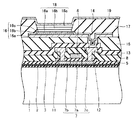
この有機EL表示装置の平面図を図1に示し、断面図を図2に示す。この有機EL表示装置は、スイッチ素子としてTFTを用いたアクティブマトリックス型の有機EL表示装置である。図1には3つの画素に相当する領域が示されている。図2は代表して1つの画素を取り出して切ったところを示している。この有機EL表示装置は、基板としてガラス基板1を備え、ガラス基板1の表面を覆うように下から順に窒化珪素膜2、酸化珪素膜3が設けられている。あるいは、ガラス基板1に窒化珪素膜2、酸化珪素膜3を合わせたものを「基板」と捉えてもよい。
A plan view of this organic EL display device is shown in FIG. 1, and a sectional view thereof is shown in FIG. This organic EL display device is an active matrix organic EL display device using TFTs as switching elements. FIG. 1 shows a region corresponding to three pixels. FIG. 2 representatively shows one pixel taken out and cut. This organic EL display device includes a
ガラス基板1の主表面には複数のTFTが設けられている。図2では複数のTFTのうち1つのみを代表的に表示している。TFTは、ポリシリコン膜7、ゲート絶縁膜5、ゲート電極6、ソース電極11およびドレイン電極12を含む。ポリシリコン膜7はチャネル領域7aを中央に有し、両端にソース領域7b、ドレイン領域7cをそれぞれ有する。ゲート絶縁膜5はポリシリコン膜7の上側を覆うように設けられている。ゲート絶縁膜5の上側にゲート電極6が配置されている。ゲート電極6の上側を覆うように第1層間絶縁膜8が設けられている。第1層間絶縁膜8の上側にソース電極11、ドレイン電極12が配置されている。ソース電極11、ドレイン電極12は第1層間絶縁膜8を貫通してソース領域7b、ドレイン領域7cにそれぞれ電気的に接続している。ソース電極11、ドレイン電極12の上側を覆うように第2層間絶縁膜13が設けられている。
A plurality of TFTs are provided on the main surface of the
第2層間絶縁膜13の上側には、上述の複数のTFTの上側を覆うように有機樹脂からなる平坦化膜15が設けられている。平坦化膜15の上側には複数のアノード電極16が設けられ、接続孔14を通じてTFTの各々に電気的に接続されている。図2では複数のアノード電極16のうち1つのみを代表的に表示している。分離膜17は有機樹脂からなり、複数のアノード電極16を個別に絶縁隔離するように形成されている。有機EL層18はアノード電極16に電気的に接続するようにアノード電極16の上側に配置されている。有機EL層18は、下から順にホール輸送層18a、発光層18b、電子輸送層18cの3層の積層構造となっている。カソード電極19は、有機EL層18に電気的に接続するように有機EL層18の上側に配置されている。アノード電極16はガラス基板1に近い側から順に、下部透明導電膜16a、反射金属膜16b、上部透明導電膜16cの3層を含む。反射金属膜16bは上面、下面および側面のすべてが透明導電膜で被覆されている。
On the upper side of the second
(作用・効果)
本実施の形態における有機EL表示装置は、反射金属膜16bの上面、下面、側面のすべてが透明導電膜により被覆され、その結果、金属膜と有機樹脂からなる膜とが直接接触する箇所がない構成となっている。したがって、長期駆動による発熱や炎天下などの高温使用環境による有機EL表示装置内部での水分とガスの発生を低減することができる。これにより、本実施の形態における有機EL表示装置は、高信頼性、長寿命の有機EL表示装置とすることができる。
(Action / Effect)
In the organic EL display device according to the present embodiment, the upper surface, the lower surface, and the side surface of the
さらに、上部透明導電膜16cと下部透明導電膜16aとが反射金属膜16bを介さずに直接電気的に接続されるため、透明導電膜に対する接触抵抗が高いAlなどの材料を反射金属膜16bに用いた場合でも、アノード電極16の抵抗を減らすことができ、発光効率が高い有機EL表示装置とすることができる。このように本実施の形態では、Alなどの材料を反射金属膜16bに用いることも問題なく行なえるので、反射金属膜16bはアルミニウムまたはアルミニウムを主成分とする合金からなることが好ましい。反射金属膜16bの光反射率を高くすることができるからである。
Further, since the upper transparent
あるいは、反射金属膜16bは銀または銀を主成分とする合金からなることが好ましい。このような構成にすれば、反射金属膜16bの電気抵抗の低くすることができるからである。
Alternatively, the
下部透明導電膜16aおよび上部透明導電膜16cは、IZO(Indium Zinc Oxide)、ITO(Indium Tin Oxide)、ZnOからなる群から選択されたいずれかの材料からなることが好ましい。容易に透明な導電膜を形成することができるからである。
The lower transparent
また、上部透明導電膜16cと下部透明導電膜16aとが反射金属膜16bを介さずに直接電気的に接続されるため、反射金属膜16bは電気的接続に寄与しないものであってもよい。したがって、電気的接続のために反射金属膜16bに従来添加していた添加物、混合物の比率を低減することができ、その結果、反射金属膜16bの反射率が向上して光の取出し効率が向上する。
Moreover, since the upper transparent
また、本実施の形態では、下部透明導電膜16aが上部透明導電膜16cより厚いことが好ましい。これは光学設計の観点からいえることである。このようにして上部透明導電膜16bの膜厚を薄く最適化すれば、光の取出し効率が向上する。下部透明導電膜によって導通は十分に図られるので、アノード電極16の抵抗増大や断線による発光不良のない有機EL表示装置とすることができる。
In the present embodiment, the lower transparent
なお、図3に示すように、反射金属膜16bの外周側面はテーパ状となっていることが好ましい。反射金属膜16bの外周側面がテーパ状となっていれば、上部透明導電膜16cの被覆性が向上するからである。そのため、反射金属膜16bと透明導電膜との接触抵抗が高くなるAl系金属などを反射金属膜16bの材料として用いた場合や、反射金属膜16bの膜厚が上部透明導電膜16cの膜厚に比べて著しく厚い場合においてもアノード電極16の抵抗を減らすことができ、発光効率が高い有機EL表示装置とすることができる。
In addition, as shown in FIG. 3, it is preferable that the outer peripheral side surface of the
(実施の形態2)
(製造方法)
図4〜図8、図2を参照して、本発明に基づく実施の形態2における有機EL表示装置の製造方法について説明する。
(Embodiment 2)
(Production method)
A method for manufacturing an organic EL display device according to the second embodiment of the present invention will be described with reference to FIGS.
本実施の形態における有機EL表示装置の製造方法は、基板の主表面に複数の薄膜トランジスタを形成する工程と、前記複数の薄膜トランジスタの上側を覆うように有機樹脂で平坦化膜を形成する工程と、前記平坦化膜の上側に、前記基板に近い側から順に、下部透明導電膜、反射金属膜、上部透明導電膜の3層をそれぞれ含む複数のアノード電極を、前記複数の薄膜トランジスタの各々に個別に電気的に接続するように形成する工程と、前記複数のアノード電極を個別に絶縁隔離しつつ、前記複数のアノード電極の一部を開口部を通じて露出させるように、有機樹脂で分離膜を形成する工程と、前記開口部内において前記アノード電極に電気的に接続するように前記アノード電極の上側に有機EL層を形成する工程と、前記有機EL層に電気的に接続するように前記有機EL層の上側にカソード電極を形成する工程とを含む。前記複数のアノード電極を形成する工程では、前記反射金属膜は上面、下面、側面のすべてが透明導電膜で被覆されるように形成される。 The manufacturing method of the organic EL display device in the present embodiment includes a step of forming a plurality of thin film transistors on the main surface of the substrate, a step of forming a planarizing film with an organic resin so as to cover the upper side of the plurality of thin film transistors, A plurality of anode electrodes each including three layers of a lower transparent conductive film, a reflective metal film, and an upper transparent conductive film are provided on each of the plurality of thin film transistors, in order from the side closer to the substrate, on the flattening film. Forming a separation membrane with an organic resin so as to expose a part of the plurality of anode electrodes through the opening while individually isolating and isolating the plurality of anode electrodes; Forming an organic EL layer on the upper side of the anode electrode so as to be electrically connected to the anode electrode in the opening; and The upper side of the organic EL layer to connect and forming a cathode electrode. In the step of forming the plurality of anode electrodes, the reflective metal film is formed so that the upper surface, the lower surface, and the side surface are all covered with the transparent conductive film.
以下、本実施の形態における有機EL表示装置の製造方法を各工程別に図面を参照しながら示す。図4に示すように、まず、基板の主表面に複数の薄膜トランジスタ(TFT)を形成する。ここでいう「基板」とは、ガラス基板1に窒化珪素膜2、酸化珪素膜3を合わせたものである。図4では1つの画素に相当する領域の断面図となっているので1つのTFTしか表示されていないが、実際には表示領域全域にわたって多数のTFTが形成される。TFTの形成は公知技術を用いて行なうことができる。
Hereinafter, a method for manufacturing an organic EL display device according to the present embodiment will be described for each process with reference to the drawings. As shown in FIG. 4, first, a plurality of thin film transistors (TFTs) are formed on the main surface of the substrate. Here, the “substrate” refers to a
次に、図5に示すように第2層間絶縁膜13を形成する。第2層間絶縁膜13は窒化珪素膜であり、CVD法で成膜することができる。写真製版技術およびエッチング技術を用いて第2層間絶縁膜13を貫通するように接続孔14の下部を形成する。さらに図5に示すように、複数のTFTの上側を覆うように有機樹脂で平坦化膜15を形成する。平坦化膜15は感光性を有したアクリル系樹脂によって形成することができる。写真製版技術により平坦化膜15を貫通するように接続孔14の上部を形成する。その後、230℃で焼成を行なう。
Next, as shown in FIG. 5, a second
さらに、図6に示すように、平坦化膜15の上側に、前記基板に近い側から順に、下部透明導電膜16a、反射金属膜16b、上部透明導電膜16cの3層をそれぞれ含む複数のアノード電極16を、前記複数のTFTの各々に個別に電気的に接続するように形成する。下部透明導電膜16aはIZOで厚み200nmになるように、反射金属膜16bはAl合金で厚み50nmになるように、それぞれスパッタ法によって連続して成膜する。このスパッタ法によって当初は広い範囲に形成される反射金属膜16bの上に、写真製版技術を用いて、下部透明導電膜16aに比べて小さな面積のみを覆うように島状のレジスト膜を形成する。このレジスト膜をマスクとしてエッチング技術を用いて反射金属膜16bをエッチングし、図6に示すように所望の領域にのみ残るようにする。このエッチングの際には、エッチング液を適当に選択することにより反射金属膜16bのエッジ、すなわち外周側面をテーパ状とすることができる。たとえば反射金属膜16bがアルミニウムからなる場合、酢酸の比率を高くしたエッチング液を用いると、外周側面をテーパ状とすることができる。その後、レジスト膜を除去する。さらにその後にUV処理やオゾン水による洗浄処理を実施する。上部透明導電膜16cはIZOで厚み20nmになるようにスパッタ法によって成膜する。上部透明導電膜16cを成膜することによって反射金属膜16bの全体が上部透明導電膜16cによって覆われる。その後、写真製版技術を用いて、反射金属膜16bより広い領域にわたるアノード電極16用のレジストパターンを形成する。エッチング技術により、上部透明導電膜16cおよび下部透明導電膜16aを同時にエッチングし、レジストパターンを除去する。このようにして、反射金属膜16bがIZOからなる透明導電膜によって完全に包み込まれ、なおかつ、全体として所望形状となったアノード電極16を得る。アノード電極16は接続孔14を通じてTFTに電気的に接続されている。
Further, as shown in FIG. 6, a plurality of anodes each including three layers of a lower transparent
さらに、図7に示すように、前記複数のアノード電極16を個別に絶縁隔離しつつ、前記複数のアノード電極16の一部を開口部を通じて露出させるように、有機樹脂で分離膜17を形成する。分離膜17は感光性を有したポリイミド樹脂によって形成することができる。写真製版技術を用いて形成し、230℃で焼成する。分離膜17は、この後の工程において真空蒸着法で有機EL層18を形成する際に用いるメタルマスクと有機EL層18が形成されるべき場所であるアノード電極16の表面とが互いに接触しないようにするためのリブ材の役割も果たす。アノード電極16表面の清浄度を高めるために、UV処理やキレート、オゾン水などによる洗浄処理を行なう。
Further, as shown in FIG. 7, a
次に、図8に示すように、前記開口部内においてアノード電極16に電気的に接続するようにアノード電極16の上側に有機EL層18を形成する。この有機EL層18の成膜は、真空加熱脱水処理の後、真空雰囲気を維持したままの状態で行なう。有機EL層18は、ホール輸送層18a、発光層18bおよび電子輸送層18cを含む有機材料の層であり、電圧を印加することにより発光する性質を有する。
Next, as shown in FIG. 8, an
さらに、有機EL層18に電気的に接続するように有機EL層18の上側にカソード電極19を形成する。このカソード電極19の形成は真空雰囲気を維持したまま行なう。こうして、図2に示す構造の有機EL表示装置を得ることができる。さらに、この有機EL表示装置の上面を保護するために、上側にカバーガラスを被せるか保護層を形成することが好ましい。
Further, a
(作用・効果)
本実施の形態における有機EL表示装置の製造方法によれば、実施の形態1で説明した有機EL表示装置を得ることができる。すなわち、反射金属膜16bの上面、下面、側面のすべてが透明導電膜により被覆され、金属膜と有機樹脂からなる膜とが直接接触する箇所がないように有機EL表示装置を製造することができる。したがって、長期駆動による発熱や炎天下などの高温使用環境による内部での水分とガスの発生を低減した有機EL表示装置を製造することができる。
(Action / Effect)
According to the method for manufacturing an organic EL display device in the present embodiment, the organic EL display device described in the first embodiment can be obtained. That is, the organic EL display device can be manufactured so that the upper surface, the lower surface, and the side surface of the
なお、実施の形態1で図3に示した構造の有機EL表示装置を得るためには、図6に示すようにアノード電極16を形成する工程において、図9に示すように、反射金属膜16bの外周側面がテーパ状となるように形成すればよい。反射金属膜16bをこのように形成すれば上部透明導電膜16cもテーパ状となる。このような工程を含ませれば、実施の形態1で図3に示した構造の有機EL表示装置を得ることができる。
In order to obtain the organic EL display device having the structure shown in FIG. 3 in the first embodiment, in the step of forming the
なお、実施の形態1,2では、アクティブマトリックス型の有機EL表示装置のスイッチ素子としてトップゲート型シングルゲートTFTを採用した例について説明したが、スイッチ素子は、スイッチ機能を有する素子であれば他のものであってもよく、たとえばボトムゲート型TFTや薄膜ダイオード、有機トランジスタであってもよい。また、本発明の適用対象となる有機EL表示装置はアクティブマトリックス型に限るものではなく、スイッチ素子を持たないパッシブマトリックス型の有機EL表示装置であってもよい。 In the first and second embodiments, the example in which the top gate type single gate TFT is employed as the switch element of the active matrix organic EL display device has been described. However, the switch element may be any element having a switch function. For example, a bottom gate TFT, a thin film diode, or an organic transistor may be used. The organic EL display device to which the present invention is applied is not limited to the active matrix type, and may be a passive matrix type organic EL display device having no switching elements.
実施の形態1,2で例示した有機EL表示装置は、トップエミッション型であったが、ボトムエミッション型であってもよい。 The organic EL display device exemplified in the first and second embodiments is a top emission type, but may be a bottom emission type.
実施の形態1,2では、透明導電膜にIZOを用いたが、ITO、ZnOなどの透明導電膜を用いてもよく、電気的接続が可能であれば上部透明導電膜16cと下部透明導電膜16aとで材質が異なってもよい。また、上部透明導電膜16cの膜厚は有機EL層の構成や透明導電膜自体の屈折率、吸収係数から決定されるべきであるため、実施の形態1,2で示したものと異なってもよい。さらに、下部透明導電膜16aは、被覆性と電気抵抗を考慮して決定されるべきであるため、実施の形態1,2で示したものと異なってもよい。
In the first and second embodiments, IZO is used for the transparent conductive film. However, a transparent conductive film such as ITO or ZnO may be used. If electrical connection is possible, the upper transparent
実施の形態1,2では、有機EL層18をホール輸送層18a、発光層18b、電子輸送層18cの3層の積層構造として説明したが、有機EL層18は、発光層18bの単層であってもよく、発光層18bを含む多層膜であってもよい。
In the first and second embodiments, the
実施の形態1,2では、平坦化膜15にはアクリル系樹脂を、分離膜17にはポリイミド系樹脂を用いた例について説明したが、平坦化膜15と分離膜17とが同じ材料であってもよく、たとえばアクリル系樹脂やポリイミド系樹脂またはエポキシ系樹脂などのうちのいずれか1種類の材料で統一してもよい。
In the first and second embodiments, an example in which an acrylic resin is used for the
有機EL素子の封止は、不活性ガスと封止材との組合せ(図示せず)によって行なうことができるが、たとえば窒化珪素膜や有機樹脂などの積層構造で行なってもよい。 The organic EL element can be sealed by a combination (not shown) of an inert gas and a sealing material, but may be a laminated structure such as a silicon nitride film or an organic resin.
本発明は有機EL表示装置に関するものであるが、金属膜と有機樹脂が接触する構造を備える表示装置、半導体装置にも適用可能である。他の種類の表示装置としては、たとえば、半透過型、反射型の液晶表示装置にも応用が可能である。液晶表示装置の場合、本発明を適用することで液晶への水分混入が低減されるので、液晶の保持容量の変動が抑えられ、焼付きがきわめて少ない液晶表示装置とすることができる。 The present invention relates to an organic EL display device, but is also applicable to a display device and a semiconductor device having a structure in which a metal film and an organic resin are in contact with each other. Other types of display devices can be applied to, for example, transflective and reflective liquid crystal display devices. In the case of a liquid crystal display device, application of the present invention reduces moisture mixing into the liquid crystal, so that variation in the storage capacity of the liquid crystal can be suppressed, and a liquid crystal display device with extremely low image sticking can be obtained.
なお、今回開示した上記実施の形態はすべての点で例示であって制限的なものではない。本発明の範囲は上記した説明ではなくて特許請求の範囲によって示され、特許請求の範囲と均等の意味および範囲内でのすべての変更を含むものである。 In addition, the said embodiment disclosed this time is an illustration in all the points, Comprising: It is not restrictive. The scope of the present invention is defined by the terms of the claims, rather than the description above, and includes all modifications within the scope and meaning equivalent to the terms of the claims.
1 ガラス基板、2 窒化珪素膜、3 酸化珪素膜、5 ゲート絶縁膜、6 ゲート電極、7 ポリシリコン膜、7a チャネル領域、7b ソース領域、7c ドレイン領域、8 第1層間絶縁膜、11 ソース電極、12 ドレイン電極、13 第2層間絶縁膜、14 接続孔、15 平坦化膜、16 アノード電極、16a 下部透明導電膜、16b 反射金属膜、16c 上部透明導電膜、17 分離膜、18 有機EL層、18a ホール輸送層、18b 発光層、18c 電子輸送層、19 カソード電極。 1 glass substrate, 2 silicon nitride film, 3 silicon oxide film, 5 gate insulating film, 6 gate electrode, 7 polysilicon film, 7a channel region, 7b source region, 7c drain region, 8 first interlayer insulating film, 11 source electrode , 12 Drain electrode, 13 Second interlayer insulating film, 14 Connection hole, 15 Planarization film, 16 Anode electrode, 16a Lower transparent conductive film, 16b Reflective metal film, 16c Upper transparent conductive film, 17 Separation film, 18 Organic EL layer , 18a hole transport layer, 18b light emitting layer, 18c electron transport layer, 19 cathode electrode.
Claims (6)
前記基板の主表面に形成された複数の薄膜トランジスタと、
前記複数の薄膜トランジスタの上側を覆い、有機樹脂からなる平坦化膜と、
前記平坦化膜の上側に配置され、前記複数の薄膜トランジスタの各々に電気的に接続された複数のアノード電極と、
前記複数のアノード電極を個別に絶縁隔離するように形成され、有機樹脂からなる分離膜と、
前記アノード電極に電気的に接続するように前記アノード電極の上側に配置された有機EL層と、
前記有機EL層に電気的に接続するように前記有機EL層の上側に配置されたカソード電極とを備え、
前記アノード電極は前記基板に近い側から順に、下部透明導電膜、反射金属膜、上部透明導電膜の3層を含み、
前記反射金属膜は上面、下面および側面のすべてが透明導電膜で被覆されており、前記下部透明導電膜と前記上部透明導電膜とは前記反射金属膜より外側に延在した部位で互いに接して積層されており、前記分離膜と前記反射金属膜とは互いに接触していない、有機EL表示装置。 A substrate,
A plurality of thin film transistors formed on the main surface of the substrate;
Covering the upper side of the plurality of thin film transistors, and a planarizing film made of an organic resin;
A plurality of anode electrodes disposed on the planarization film and electrically connected to each of the plurality of thin film transistors;
A plurality of anode electrodes, each of which is formed so as to be insulated and isolated, and a separation membrane made of an organic resin;
An organic EL layer disposed on the anode electrode so as to be electrically connected to the anode electrode;
A cathode electrode disposed on the organic EL layer so as to be electrically connected to the organic EL layer;
The anode electrode includes three layers of a lower transparent conductive film, a reflective metal film, and an upper transparent conductive film in order from the side close to the substrate,
The reflective metal film top surface, all of the lower surface and side surfaces are coated with a transparent conductive film, the previous SL lower transparent conductive film and the upper transparent conductive film in contact with each other at the site extending outward from the reflective metal layer An organic EL display device in which the separation film and the reflective metal film are not in contact with each other .
前記複数の薄膜トランジスタの上側を覆うように有機樹脂で平坦化膜を形成する工程と、
前記平坦化膜の上側に、前記基板に近い側から順に、下部透明導電膜、反射金属膜、上部透明導電膜の3層をそれぞれ含む複数のアノード電極を、前記複数の薄膜トランジスタの各々に個別に電気的に接続するように形成する工程と、
前記複数のアノード電極を個別に絶縁隔離しつつ、前記複数のアノード電極の一部を開口部を通じて露出させるように、有機樹脂で分離膜を形成する工程と、
前記開口部内において前記アノード電極に電気的に接続するように前記アノード電極の上側に有機EL層を形成する工程と、
前記有機EL層に電気的に接続するように前記有機EL層の上側にカソード電極を形成する工程とを含み、
前記複数のアノード電極を形成する工程では、前記反射金属膜は上面、下面、側面のすべてが透明導電膜で被覆されるように形成され、前記下部透明導電膜と前記上部透明導電膜とは前記反射金属膜より外側に延在した部位で互いに接して積層するように形成され、前記分離膜と前記反射金属膜とは互いに接触しない、有機EL表示装置の製造方法。 Forming a plurality of thin film transistors on the main surface of the substrate;
Forming a planarization film with an organic resin so as to cover the upper side of the plurality of thin film transistors;
A plurality of anode electrodes each including three layers of a lower transparent conductive film, a reflective metal film, and an upper transparent conductive film are provided on each of the plurality of thin film transistors, in order from the side closer to the substrate, on the flattening film. Forming to be electrically connected;
Forming a separation membrane with an organic resin so as to expose a part of the plurality of anode electrodes through the opening while individually isolating and isolating the plurality of anode electrodes;
Forming an organic EL layer above the anode electrode so as to be electrically connected to the anode electrode in the opening;
Forming a cathode electrode on the upper side of the organic EL layer so as to be electrically connected to the organic EL layer,
In the step of forming the plurality of anode electrodes, the reflective metal film is formed such that the upper surface, the lower surface, and the side surface are all covered with a transparent conductive film, and the lower transparent conductive film and the upper transparent conductive film are A method for manufacturing an organic EL display device , wherein the separation film and the reflective metal film are not in contact with each other, and are formed so as to be stacked in contact with each other at a portion extending outward from the reflective metal film .
Priority Applications (1)
| Application Number | Priority Date | Filing Date | Title |
|---|---|---|---|
| JP2006148415A JP4864546B2 (en) | 2006-05-29 | 2006-05-29 | Organic EL display device and manufacturing method thereof |
Applications Claiming Priority (1)
| Application Number | Priority Date | Filing Date | Title |
|---|---|---|---|
| JP2006148415A JP4864546B2 (en) | 2006-05-29 | 2006-05-29 | Organic EL display device and manufacturing method thereof |
Publications (2)
| Publication Number | Publication Date |
|---|---|
| JP2007317606A JP2007317606A (en) | 2007-12-06 |
| JP4864546B2 true JP4864546B2 (en) | 2012-02-01 |
Family
ID=38851274
Family Applications (1)
| Application Number | Title | Priority Date | Filing Date |
|---|---|---|---|
| JP2006148415A Expired - Fee Related JP4864546B2 (en) | 2006-05-29 | 2006-05-29 | Organic EL display device and manufacturing method thereof |
Country Status (1)
| Country | Link |
|---|---|
| JP (1) | JP4864546B2 (en) |
Families Citing this family (18)
| Publication number | Priority date | Publication date | Assignee | Title |
|---|---|---|---|---|
| JP5006108B2 (en) * | 2007-06-01 | 2012-08-22 | 株式会社ジャパンディスプレイイースト | Display device |
| TWI375070B (en) | 2008-04-25 | 2012-10-21 | Chimei Innolux Corp | Active matrix display and image display system using the active matrix display |
| JP4998412B2 (en) * | 2008-09-03 | 2012-08-15 | カシオ計算機株式会社 | Method for manufacturing electroluminescence panel |
| KR101146980B1 (en) | 2009-02-17 | 2012-05-22 | 삼성모바일디스플레이주식회사 | Organic light emitting diode and manufacturing method thereof |
| CN104752465B (en) * | 2013-12-30 | 2018-01-05 | 昆山工研院新型平板显示技术中心有限公司 | Array base palte of top emitting organic light emitting display and preparation method thereof |
| JP2016100402A (en) * | 2014-11-19 | 2016-05-30 | 日本放送協会 | Thin film device and manufacturing method of the same |
| KR102384945B1 (en) * | 2015-01-02 | 2022-04-08 | 삼성디스플레이 주식회사 | Organic light emitting diode display and method of manufacturing the same |
| KR102452198B1 (en) * | 2015-05-28 | 2022-10-07 | 엘지디스플레이 주식회사 | Organic light emitting display device and method of manufacturing the same |
| KR102545253B1 (en) * | 2015-05-28 | 2023-06-19 | 엘지디스플레이 주식회사 | Organic light emitting display device and method of manufacturing the same |
| KR102483434B1 (en) * | 2015-05-28 | 2022-12-30 | 엘지디스플레이 주식회사 | Organic light emitting display device and method of manufacturing the same |
| KR102515033B1 (en) * | 2015-05-29 | 2023-03-28 | 엘지디스플레이 주식회사 | Organic light emitting display device and method of manufacturing the same |
| CN105118836B (en) * | 2015-07-29 | 2019-04-05 | 京东方科技集团股份有限公司 | Array substrate and preparation method thereof with conductive flatness layer |
| JP6685142B2 (en) | 2016-02-02 | 2020-04-22 | 株式会社ジャパンディスプレイ | Display device and manufacturing method thereof |
| KR102378305B1 (en) * | 2017-05-31 | 2022-03-23 | 엘지디스플레이 주식회사 | Flexible display device |
| US10581011B2 (en) * | 2018-06-01 | 2020-03-03 | Int Tech Co., Ltd. | Light emitting device with different light emitting material overlapping width |
| US11251244B2 (en) | 2018-06-01 | 2022-02-15 | Int Tech Co., Ltd. | Light-emitting device |
| JP7414730B2 (en) * | 2018-11-20 | 2024-01-16 | ソニーセミコンダクタソリューションズ株式会社 | Display device, display device manufacturing method, and electronic equipment |
| CN115210794B (en) * | 2020-03-02 | 2023-10-17 | 夏普株式会社 | Display device and method for manufacturing the same |
Family Cites Families (9)
| Publication number | Priority date | Publication date | Assignee | Title |
|---|---|---|---|---|
| GB9712483D0 (en) * | 1997-06-17 | 1997-08-20 | Kathirgamanathan Poopathy | Fabrication of light emitting devices from chelates of transition metals, lanthanides and actinides |
| JP2003323131A (en) * | 2002-05-08 | 2003-11-14 | Sharp Corp | Electrode board for display and display device |
| KR100477746B1 (en) * | 2002-06-22 | 2005-03-18 | 삼성에스디아이 주식회사 | Organic electroluminescence device employing multi-layered anode |
| JP4062171B2 (en) * | 2003-05-28 | 2008-03-19 | ソニー株式会社 | Manufacturing method of laminated structure |
| JP2005011793A (en) * | 2003-05-29 | 2005-01-13 | Sony Corp | Manufacturing method of structure of lamination, lamination structure, display element and display device |
| JP2005005068A (en) * | 2003-06-11 | 2005-01-06 | Toppoly Optoelectronics Corp | Light emitting element having reflection prevention structure |
| JP4461726B2 (en) * | 2003-07-16 | 2010-05-12 | ソニー株式会社 | ORGANIC LIGHT EMITTING ELEMENT, ITS MANUFACTURING METHOD, AND DISPLAY DEVICE |
| JP2005322564A (en) * | 2004-05-11 | 2005-11-17 | Sony Corp | Manufacturing method of display device, and display device |
| JP2005208678A (en) * | 2005-03-28 | 2005-08-04 | Hitachi Ltd | Liquid crystal display |
-
2006
- 2006-05-29 JP JP2006148415A patent/JP4864546B2/en not_active Expired - Fee Related
Also Published As
| Publication number | Publication date |
|---|---|
| JP2007317606A (en) | 2007-12-06 |
Similar Documents
| Publication | Publication Date | Title |
|---|---|---|
| JP4864546B2 (en) | Organic EL display device and manufacturing method thereof | |
| US11011730B2 (en) | Display device and organic luminescent display device | |
| TWI729456B (en) | Display apparatus | |
| TWI578593B (en) | Organic light emitting diode device and method for fabricating the same | |
| TWI387104B (en) | Light emitting apparatus and method of manufacturing the same | |
| JP4745266B2 (en) | Organic electroluminescent display device and manufacturing method thereof | |
| US8212258B2 (en) | Display device and method for manufacturing display device | |
| US8008857B2 (en) | Organic light emitting display with reflective electrode | |
| TW201523841A (en) | Organic light-emitting diode (OLED) display | |
| US8841832B2 (en) | Organic light emitting diode display having improved strength by preventing the exfoliation of a sealant | |
| JP4637831B2 (en) | ORGANIC ELECTROLUMINESCENCE ELEMENT, ITS MANUFACTURING METHOD, AND DISPLAY DEVICE | |
| CN104733471A (en) | Array substrate of organic light-emitting displaying device and preparing method thereof | |
| TW201445729A (en) | Organic light-emitting display device | |
| EP1505666B1 (en) | Top-emission active matrix organic electroluminescent display device and method for fabricating the same | |
| TWI237525B (en) | Electro-luminescence display device and method for forming the same | |
| WO2014084051A1 (en) | Oxide semiconductor element, method for manufacturing oxide semiconductor element, display device and image sensor | |
| JP5117553B2 (en) | Manufacturing method of display device | |
| KR20120061541A (en) | Organic electro-luminescent Device | |
| CN1292394C (en) | Electroluminescent display device and its producing method | |
| KR100615220B1 (en) | Thin film transistor and flat display employing the same | |
| KR100635070B1 (en) | Organic Electro-Luminescence device and method for fabricating of the same | |
| KR20160016349A (en) | Organic light emitting display device and method of manufacturing the same |
Legal Events
| Date | Code | Title | Description |
|---|---|---|---|
| A621 | Written request for application examination |
Free format text: JAPANESE INTERMEDIATE CODE: A621 Effective date: 20081217 |
|
| A977 | Report on retrieval |
Free format text: JAPANESE INTERMEDIATE CODE: A971007 Effective date: 20101207 |
|
| A131 | Notification of reasons for refusal |
Free format text: JAPANESE INTERMEDIATE CODE: A131 Effective date: 20110125 |
|
| A521 | Request for written amendment filed |
Free format text: JAPANESE INTERMEDIATE CODE: A523 Effective date: 20110323 |
|
| A131 | Notification of reasons for refusal |
Free format text: JAPANESE INTERMEDIATE CODE: A131 Effective date: 20110621 |
|
| A521 | Request for written amendment filed |
Free format text: JAPANESE INTERMEDIATE CODE: A523 Effective date: 20110809 |
|
| TRDD | Decision of grant or rejection written | ||
| A01 | Written decision to grant a patent or to grant a registration (utility model) |
Free format text: JAPANESE INTERMEDIATE CODE: A01 Effective date: 20111101 |
|
| A01 | Written decision to grant a patent or to grant a registration (utility model) |
Free format text: JAPANESE INTERMEDIATE CODE: A01 |
|
| A61 | First payment of annual fees (during grant procedure) |
Free format text: JAPANESE INTERMEDIATE CODE: A61 Effective date: 20111109 |
|
| FPAY | Renewal fee payment (event date is renewal date of database) |
Free format text: PAYMENT UNTIL: 20141118 Year of fee payment: 3 |
|
| R150 | Certificate of patent or registration of utility model |
Free format text: JAPANESE INTERMEDIATE CODE: R150 |
|
| R250 | Receipt of annual fees |
Free format text: JAPANESE INTERMEDIATE CODE: R250 |
|
| R250 | Receipt of annual fees |
Free format text: JAPANESE INTERMEDIATE CODE: R250 |
|
| LAPS | Cancellation because of no payment of annual fees |