JP4862369B2 - Self-luminous display device, peak luminance adjusting device, electronic device, peak luminance adjusting method and program - Google Patents
Self-luminous display device, peak luminance adjusting device, electronic device, peak luminance adjusting method and program Download PDFInfo
- Publication number
- JP4862369B2 JP4862369B2 JP2005340436A JP2005340436A JP4862369B2 JP 4862369 B2 JP4862369 B2 JP 4862369B2 JP 2005340436 A JP2005340436 A JP 2005340436A JP 2005340436 A JP2005340436 A JP 2005340436A JP 4862369 B2 JP4862369 B2 JP 4862369B2
- Authority
- JP
- Japan
- Prior art keywords
- peak luminance
- gradation value
- average gradation
- power consumption
- period
- Prior art date
- Legal status (The legal status is an assumption and is not a legal conclusion. Google has not performed a legal analysis and makes no representation as to the accuracy of the status listed.)
- Active
Links
- 238000000034 method Methods 0.000 title claims description 21
- 238000004364 calculation method Methods 0.000 claims description 19
- 230000008569 process Effects 0.000 claims description 7
- 235000019557 luminance Nutrition 0.000 claims 50
- 238000004590 computer program Methods 0.000 claims 2
- 230000006870 function Effects 0.000 description 7
- 230000006641 stabilisation Effects 0.000 description 7
- 238000011105 stabilization Methods 0.000 description 7
- 239000003990 capacitor Substances 0.000 description 4
- 238000010586 diagram Methods 0.000 description 4
- 230000004044 response Effects 0.000 description 3
- 239000000758 substrate Substances 0.000 description 3
- 238000006243 chemical reaction Methods 0.000 description 2
- 230000001934 delay Effects 0.000 description 2
- 230000004048 modification Effects 0.000 description 2
- 238000012986 modification Methods 0.000 description 2
- 239000004065 semiconductor Substances 0.000 description 2
- 230000001629 suppression Effects 0.000 description 2
- 230000007704 transition Effects 0.000 description 2
- 101150059062 apln gene Proteins 0.000 description 1
- 230000000694 effects Effects 0.000 description 1
- 230000003760 hair shine Effects 0.000 description 1
- 238000003384 imaging method Methods 0.000 description 1
- 230000006872 improvement Effects 0.000 description 1
- 230000010365 information processing Effects 0.000 description 1
- 239000011159 matrix material Substances 0.000 description 1
- 230000002093 peripheral effect Effects 0.000 description 1
- 230000009467 reduction Effects 0.000 description 1
- 230000001360 synchronised effect Effects 0.000 description 1
Images


Classifications
-
- G—PHYSICS
- G09—EDUCATION; CRYPTOGRAPHY; DISPLAY; ADVERTISING; SEALS
- G09G—ARRANGEMENTS OR CIRCUITS FOR CONTROL OF INDICATING DEVICES USING STATIC MEANS TO PRESENT VARIABLE INFORMATION
- G09G3/00—Control arrangements or circuits, of interest only in connection with visual indicators other than cathode-ray tubes
- G09G3/20—Control arrangements or circuits, of interest only in connection with visual indicators other than cathode-ray tubes for presentation of an assembly of a number of characters, e.g. a page, by composing the assembly by combination of individual elements arranged in a matrix no fixed position being assigned to or needed to be assigned to the individual characters or partial characters
- G09G3/22—Control arrangements or circuits, of interest only in connection with visual indicators other than cathode-ray tubes for presentation of an assembly of a number of characters, e.g. a page, by composing the assembly by combination of individual elements arranged in a matrix no fixed position being assigned to or needed to be assigned to the individual characters or partial characters using controlled light sources
- G09G3/30—Control arrangements or circuits, of interest only in connection with visual indicators other than cathode-ray tubes for presentation of an assembly of a number of characters, e.g. a page, by composing the assembly by combination of individual elements arranged in a matrix no fixed position being assigned to or needed to be assigned to the individual characters or partial characters using controlled light sources using electroluminescent panels
- G09G3/32—Control arrangements or circuits, of interest only in connection with visual indicators other than cathode-ray tubes for presentation of an assembly of a number of characters, e.g. a page, by composing the assembly by combination of individual elements arranged in a matrix no fixed position being assigned to or needed to be assigned to the individual characters or partial characters using controlled light sources using electroluminescent panels semiconductive, e.g. using light-emitting diodes [LED]
- G09G3/3208—Control arrangements or circuits, of interest only in connection with visual indicators other than cathode-ray tubes for presentation of an assembly of a number of characters, e.g. a page, by composing the assembly by combination of individual elements arranged in a matrix no fixed position being assigned to or needed to be assigned to the individual characters or partial characters using controlled light sources using electroluminescent panels semiconductive, e.g. using light-emitting diodes [LED] organic, e.g. using organic light-emitting diodes [OLED]
- G09G3/3225—Control arrangements or circuits, of interest only in connection with visual indicators other than cathode-ray tubes for presentation of an assembly of a number of characters, e.g. a page, by composing the assembly by combination of individual elements arranged in a matrix no fixed position being assigned to or needed to be assigned to the individual characters or partial characters using controlled light sources using electroluminescent panels semiconductive, e.g. using light-emitting diodes [LED] organic, e.g. using organic light-emitting diodes [OLED] using an active matrix
- G09G3/3233—Control arrangements or circuits, of interest only in connection with visual indicators other than cathode-ray tubes for presentation of an assembly of a number of characters, e.g. a page, by composing the assembly by combination of individual elements arranged in a matrix no fixed position being assigned to or needed to be assigned to the individual characters or partial characters using controlled light sources using electroluminescent panels semiconductive, e.g. using light-emitting diodes [LED] organic, e.g. using organic light-emitting diodes [OLED] using an active matrix with pixel circuitry controlling the current through the light-emitting element
-
- G—PHYSICS
- G09—EDUCATION; CRYPTOGRAPHY; DISPLAY; ADVERTISING; SEALS
- G09G—ARRANGEMENTS OR CIRCUITS FOR CONTROL OF INDICATING DEVICES USING STATIC MEANS TO PRESENT VARIABLE INFORMATION
- G09G3/00—Control arrangements or circuits, of interest only in connection with visual indicators other than cathode-ray tubes
- G09G3/20—Control arrangements or circuits, of interest only in connection with visual indicators other than cathode-ray tubes for presentation of an assembly of a number of characters, e.g. a page, by composing the assembly by combination of individual elements arranged in a matrix no fixed position being assigned to or needed to be assigned to the individual characters or partial characters
- G09G3/22—Control arrangements or circuits, of interest only in connection with visual indicators other than cathode-ray tubes for presentation of an assembly of a number of characters, e.g. a page, by composing the assembly by combination of individual elements arranged in a matrix no fixed position being assigned to or needed to be assigned to the individual characters or partial characters using controlled light sources
- G09G3/28—Control arrangements or circuits, of interest only in connection with visual indicators other than cathode-ray tubes for presentation of an assembly of a number of characters, e.g. a page, by composing the assembly by combination of individual elements arranged in a matrix no fixed position being assigned to or needed to be assigned to the individual characters or partial characters using controlled light sources using luminous gas-discharge panels, e.g. plasma panels
- G09G3/288—Control arrangements or circuits, of interest only in connection with visual indicators other than cathode-ray tubes for presentation of an assembly of a number of characters, e.g. a page, by composing the assembly by combination of individual elements arranged in a matrix no fixed position being assigned to or needed to be assigned to the individual characters or partial characters using controlled light sources using luminous gas-discharge panels, e.g. plasma panels using AC panels
- G09G3/291—Control arrangements or circuits, of interest only in connection with visual indicators other than cathode-ray tubes for presentation of an assembly of a number of characters, e.g. a page, by composing the assembly by combination of individual elements arranged in a matrix no fixed position being assigned to or needed to be assigned to the individual characters or partial characters using controlled light sources using luminous gas-discharge panels, e.g. plasma panels using AC panels controlling the gas discharge to control a cell condition, e.g. by means of specific pulse shapes
-
- G—PHYSICS
- G09—EDUCATION; CRYPTOGRAPHY; DISPLAY; ADVERTISING; SEALS
- G09G—ARRANGEMENTS OR CIRCUITS FOR CONTROL OF INDICATING DEVICES USING STATIC MEANS TO PRESENT VARIABLE INFORMATION
- G09G3/00—Control arrangements or circuits, of interest only in connection with visual indicators other than cathode-ray tubes
- G09G3/20—Control arrangements or circuits, of interest only in connection with visual indicators other than cathode-ray tubes for presentation of an assembly of a number of characters, e.g. a page, by composing the assembly by combination of individual elements arranged in a matrix no fixed position being assigned to or needed to be assigned to the individual characters or partial characters
- G09G3/22—Control arrangements or circuits, of interest only in connection with visual indicators other than cathode-ray tubes for presentation of an assembly of a number of characters, e.g. a page, by composing the assembly by combination of individual elements arranged in a matrix no fixed position being assigned to or needed to be assigned to the individual characters or partial characters using controlled light sources
- G09G3/30—Control arrangements or circuits, of interest only in connection with visual indicators other than cathode-ray tubes for presentation of an assembly of a number of characters, e.g. a page, by composing the assembly by combination of individual elements arranged in a matrix no fixed position being assigned to or needed to be assigned to the individual characters or partial characters using controlled light sources using electroluminescent panels
- G09G3/32—Control arrangements or circuits, of interest only in connection with visual indicators other than cathode-ray tubes for presentation of an assembly of a number of characters, e.g. a page, by composing the assembly by combination of individual elements arranged in a matrix no fixed position being assigned to or needed to be assigned to the individual characters or partial characters using controlled light sources using electroluminescent panels semiconductive, e.g. using light-emitting diodes [LED]
-
- G—PHYSICS
- G09—EDUCATION; CRYPTOGRAPHY; DISPLAY; ADVERTISING; SEALS
- G09G—ARRANGEMENTS OR CIRCUITS FOR CONTROL OF INDICATING DEVICES USING STATIC MEANS TO PRESENT VARIABLE INFORMATION
- G09G2300/00—Aspects of the constitution of display devices
- G09G2300/08—Active matrix structure, i.e. with use of active elements, inclusive of non-linear two terminal elements, in the pixels together with light emitting or modulating elements
- G09G2300/0809—Several active elements per pixel in active matrix panels
- G09G2300/0842—Several active elements per pixel in active matrix panels forming a memory circuit, e.g. a dynamic memory with one capacitor
- G09G2300/0861—Several active elements per pixel in active matrix panels forming a memory circuit, e.g. a dynamic memory with one capacitor with additional control of the display period without amending the charge stored in a pixel memory, e.g. by means of additional select electrodes
-
- G—PHYSICS
- G09—EDUCATION; CRYPTOGRAPHY; DISPLAY; ADVERTISING; SEALS
- G09G—ARRANGEMENTS OR CIRCUITS FOR CONTROL OF INDICATING DEVICES USING STATIC MEANS TO PRESENT VARIABLE INFORMATION
- G09G2330/00—Aspects of power supply; Aspects of display protection and defect management
- G09G2330/02—Details of power systems and of start or stop of display operation
- G09G2330/021—Power management, e.g. power saving
-
- G—PHYSICS
- G09—EDUCATION; CRYPTOGRAPHY; DISPLAY; ADVERTISING; SEALS
- G09G—ARRANGEMENTS OR CIRCUITS FOR CONTROL OF INDICATING DEVICES USING STATIC MEANS TO PRESENT VARIABLE INFORMATION
- G09G2330/00—Aspects of power supply; Aspects of display protection and defect management
- G09G2330/02—Details of power systems and of start or stop of display operation
- G09G2330/025—Reduction of instantaneous peaks of current
-
- G—PHYSICS
- G09—EDUCATION; CRYPTOGRAPHY; DISPLAY; ADVERTISING; SEALS
- G09G—ARRANGEMENTS OR CIRCUITS FOR CONTROL OF INDICATING DEVICES USING STATIC MEANS TO PRESENT VARIABLE INFORMATION
- G09G3/00—Control arrangements or circuits, of interest only in connection with visual indicators other than cathode-ray tubes
- G09G3/20—Control arrangements or circuits, of interest only in connection with visual indicators other than cathode-ray tubes for presentation of an assembly of a number of characters, e.g. a page, by composing the assembly by combination of individual elements arranged in a matrix no fixed position being assigned to or needed to be assigned to the individual characters or partial characters
- G09G3/2007—Display of intermediate tones
- G09G3/2014—Display of intermediate tones by modulation of the duration of a single pulse during which the logic level remains constant
Landscapes
- Engineering & Computer Science (AREA)
- Physics & Mathematics (AREA)
- Computer Hardware Design (AREA)
- General Physics & Mathematics (AREA)
- Theoretical Computer Science (AREA)
- Power Engineering (AREA)
- Plasma & Fusion (AREA)
- Control Of Indicators Other Than Cathode Ray Tubes (AREA)
- Electroluminescent Light Sources (AREA)
- Control Of El Displays (AREA)
- Transforming Electric Information Into Light Information (AREA)
Description
この明細書で説明する発明は、自発光表示パネル(装置)で消費される電力を規定範囲内に強制的に抑制する技術に関する。
なお、発明者らが提案する発明は、自発光表示装置、ピーク輝度調整装置、電子機器、ピーク輝度調整方法及びプログラムとしての側面を有する。
The invention described in this specification relates to a technique for forcibly suppressing power consumed by a self-luminous display panel (device) within a specified range.
The invention proposed by the inventors has aspects such as a self-luminous display device, a peak luminance adjusting device, an electronic device, a peak luminance adjusting method, and a program.
有機ELディスプレイは、広視野角特性、応答速度、広色再現性範囲、高コントラスト性能に優れるだけでなく、表示パネル自体を薄く形成することができる。これらの利点により、有機ELディスプレイは、次世代フラットパネルディスプレイの最有力候補として注目されている。 The organic EL display not only has excellent wide viewing angle characteristics, response speed, wide color reproducibility range, and high contrast performance, but also allows the display panel itself to be formed thin. Due to these advantages, the organic EL display is attracting attention as the most promising candidate for the next generation flat panel display.
さらに昨今では、応答速度やコントラス性能を発光時間の可変制御を通じて改善する手法が検討されている。発光時間の可変制御技術を開示する公知技術には、例えば以下に示す特許文献1〜3がある。
ところで、特許文献1〜3に開示された各発明は、いずれも画質の向上を目的として検討されたものであるが、定消費電力化や消費電力の抑制化についての視点は検討されていない。
実際、有機ELディスプレイその他の自発光表示装置では、一定輝度のパックライトを常時点灯状態させる方式の表示装置とは異なり、入力される映像信号に応じて表示パネルに流れる電流量が劇的に変化する特性がある。
By the way, although each invention disclosed by patent documents 1-3 is all examined for the purpose of the improvement of image quality, the viewpoint about the constant power consumption reduction or the suppression of power consumption is not examined.
In fact, in organic EL displays and other self-luminous display devices, the amount of current that flows through the display panel changes dramatically in response to the input video signal, unlike display devices that constantly turn on a pack light of constant brightness. There is a characteristic to do.
この特性のため、自発光表示装置における単位時間当たりの消費電力は一定にはならない。すなわち、表示パネルの消費電力が表示内容に応じて極端に変化する問題がある。また、表示パネルを搭載する電子機器がバッテリー駆動される場合には、表示内容に応じて使用時間が極端に変化する問題がある。この問題を解決するには、バッテリー容量を大型化する必要がある。 Because of this characteristic, the power consumption per unit time in the self-luminous display device is not constant. That is, there is a problem that the power consumption of the display panel changes extremely according to the display contents. Further, when an electronic device equipped with a display panel is driven by a battery, there is a problem that the usage time changes extremely according to the display contents. To solve this problem, it is necessary to increase the battery capacity.
発明者らは、自発光パネル面のピーク輝度を1フレーム単位で調整するピーク輝度調整装置として、以下の各機能を搭載するものを提案する。
(a)1フレーム期間中に入力される映像信号の平均階調値を算出する平均階調値算出部
(b)算出された平均階調値に応じた標準ピーク輝度を求め、当該標準ピーク輝度と算出された平均階調値で消費される消費電力量を算出する消費電力算出部
(c)一定期間内に消費される消費電力の合計値が設定電力量を超えないように、標準ピーク輝度を調整するピーク輝度調整部
Inventors propose what equips the following functions as a peak luminance adjustment apparatus which adjusts the peak luminance of a self-light-emitting panel surface per frame.
(A) An average gradation value calculation unit for calculating an average gradation value of a video signal input during one frame period. (B) Obtaining a standard peak luminance corresponding to the calculated average gradation value, and calculating the standard peak luminance. (C) A power consumption calculation unit that calculates the power consumption amount consumed at the calculated average gradation value. (C) The standard peak brightness so that the total value of the power consumption consumed within a certain period does not exceed the set power amount. Adjust the peak brightness
発明に係る手法の採用により、自発光パネルで消費される電力量を定量化又は一定量以下に抑制することができる。
を実現できる。
By employing the method according to the invention, the amount of power consumed by the self-luminous panel can be quantified or suppressed to a certain amount or less.
Can be realized.
以下、発明に係る処理機能を搭載した有機ELパネルモジュールについて説明する。
なお、本明細書で特に図示又は記載されない部分には、当該技術分野の周知又は公知技術を適用する。
また以下に説明する形態例は、発明の一つの形態例であって、これらに限定されるものではない。
Hereinafter, an organic EL panel module equipped with the processing function according to the invention will be described.
In addition, the well-known or well-known technique of the said technical field is applied to the part which is not illustrated or described in particular in this specification.
Moreover, the form example demonstrated below is one form example of invention, Comprising: It is not limited to these.
(A)ピーク輝度の調整
表示パネルのピーク輝度は、最大データの入力時に表示素子に印加される出力電圧(出力電流)又は発光時間の可変制御により調整することができる。
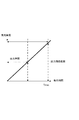
図1に、発光時間と発光輝度との関係を示す。図1に示すように、発光輝度は発光時間に対して線形に変化する。
図2(A)に、表示素子に印加される出力電圧と発光輝度との関係を示す。図2(B)に、入力映像信号の階調値(%)と表示素子に印加される出力電圧(基準値を100%で表す。)との間の入出力関係を示す。
(A) Adjustment of peak luminance The peak luminance of the display panel can be adjusted by variably controlling the output voltage (output current) or the light emission time applied to the display element when the maximum data is input.
FIG. 1 shows the relationship between the light emission time and the light emission luminance. As shown in FIG. 1, the light emission luminance changes linearly with respect to the light emission time.
FIG. 2A shows the relationship between the output voltage applied to the display element and the light emission luminance. FIG. 2B shows an input / output relationship between the gradation value (%) of the input video signal and the output voltage (reference value is represented by 100%) applied to the display element.
ここで、図2(B)に実線で示す曲線は基準値に対応する入出力関係であり、破線で示す曲線は最大データの入力時に表示素子に印加される最大出力電圧Vmax (最大出力電流Imax )を可変制御した場合の入出力関係を示す。図2に示すように、同じ入力階調値でも最大出力電圧Vmax (最大出力電流Imax )を可変制御すると、発光輝度が可変制御される。 Here, the curve indicated by the solid line in FIG. 2B is the input / output relationship corresponding to the reference value, and the curve indicated by the broken line is the maximum output voltage V max (maximum output current) applied to the display element when the maximum data is input. The input / output relationship when variably controlling (I max ) is shown. As shown in FIG. 2, when the maximum output voltage V max (maximum output current I max ) is variably controlled even with the same input gradation value, the light emission luminance is variably controlled.
さて、表示パネルのピーク輝度は、最大出力電圧Vmax (最大出力電流Imax )と発光時間との積Sで与えられる。
従って、発光時間又は最大出力電圧Vmax (最大出力電流Imax )を個別に可変制御すれば、表示パネルのピーク輝度を可変制御することが可能となる。
The peak luminance of the display panel is given by the product S of the maximum output voltage V max (maximum output current I max ) and the light emission time.
Therefore, if the light emission time or the maximum output voltage V max (maximum output current I max) by individually variably controlled, it is possible to variably control the peak brightness of the display panel.
(B)有機ELパネルの構造例
続いて、ピーク輝度の可変制御を可能とする有機ELパネルモジュールの構造例を説明する。
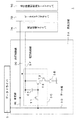
図3に、有機ELパネルモジュール1の構造例を示す。有機ELパネルモジュール1は、発光領域3A(有機EL素子がマトリクス状に配列された領域)と、画像の表示を制御するパネル駆動回路とで構成される。
パネル駆動回路は、データドライバ5、最大出力電圧制御用ドライバ7A、ゲートスキャンドライバ7B、点灯時間制御用ゲートドライバ7Cで構成される。なお、パネル駆動回路は、発光領域3Aの周辺部に形成する。
(B) Structural Example of Organic EL Panel Next, a structural example of an organic EL panel module that enables variable control of peak luminance will be described.
FIG. 3 shows a structural example of the organic
The panel drive circuit includes a
各画素に対応する有機EL素子3Bとその駆動回路(画素駆動回路)3Cは、データ線3Dと走査線3Eの交点位置に配置されている。画素駆動回路3Cは、データスイッチ素子T1、キャパシタC1、電流駆動素子T2、点灯スイッチ素子T3で構成される。
このうち、データスイッチ素子T1は、データ線3Dを通じて与えられる電圧値の取り込みタイミングを制御するのに用いられる。取り込みタイミングは、走査線3Eを通じて線順次で与えられる。
The
Among these, the data switch element T1 is used to control the timing of taking in the voltage value given through the data line 3D. The capture timing is given line-sequentially through the scanning line 3E.
キャパシタC1は、取り込んだ電圧値を1フレームの間保持するのに用いられる。キャパシタC1を用いることで、面順次駆動が実現される。
電流駆動素子T2は、キャパシタC1の電圧値に応じた電流を有機EL素子3Bに供給するのに用いられる。駆動電流は、電流供給線3Fを通じて供給される。なお、この電流供給線3Fには、最大出力電圧制御用ドライバ7Aを通じて最大出力電圧Vmax が印加される。
The capacitor C1 is used to hold the acquired voltage value for one frame. By using the capacitor C1, frame sequential driving is realized.
The current driving element T2 is used to supply a current corresponding to the voltage value of the capacitor C1 to the
点灯スイッチ素子T3は、有機EL素子3Bに対する駆動電流の供給を制御するのに用いられる。点灯スイッチ素子T3は、駆動電流の供給経路に対して直列に配置される。点灯スイッチ素子T3が閉じている間、有機EL素子3Bが点灯する。一方、点灯スイッチ素子T3が開いている間、有機EL素子3Bが消灯する。
この点灯スイッチ素子T3の開閉動作を制御するデューティパルス(図4(B))を供給するのが点灯制御線3Gである。なお、図4(A)は、基準期間としての1フレーム期間を示す。
The lighting switch element T3 is used to control the supply of drive current to the
The lighting control line 3G supplies a duty pulse (FIG. 4B) for controlling the opening / closing operation of the lighting switch element T3. Note that FIG. 4A illustrates one frame period as a reference period.
ここで、電流供給線3Fに印加する電圧の可変制御は、最大出力電圧制御用ドライバ7Aが実行する。また、発光時間の可変制御は、点灯時間制御用ゲートドライバ7Cが実行する。これらドライバの制御信号は、後述する発光条件制御装置より供給される。
なお、ピーク輝度を発光時間長で制御する場合には、最大出力電圧制御用ドライバ7Aは全てのフレームについて固定電圧を供給する。一方、ピーク輝度を最大出力電圧Vmax で制御する場合には、点灯時間制御用ゲートドライバ7Cは、全てのフレームについて固定比のデューティパルスを供給する。
Here, variable control of the voltage applied to the
When the peak luminance is controlled by the light emission time length, the maximum output
図5に、画素駆動回路3Cを形成した発光領域3Aを搭載する有機ELパネルモジュール1の構造例を示す。図5の場合、ピーク輝度調整装置11は、タイミングジェネレータ9の一部分として実装する。
なお、発光領域3Aの周辺回路(パネル駆動回路)は、半導体集積回路としてパネル基板上に搭載しても良いし、パネル基板上に半導体プロセスを用いて直接形成しても良い。
FIG. 5 shows a structural example of the organic
The peripheral circuit (panel drive circuit) of the light emitting region 3A may be mounted on the panel substrate as a semiconductor integrated circuit, or may be directly formed on the panel substrate using a semiconductor process.
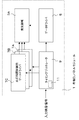
(C)ピーク輝度調整装置の形態例
以下、一定期間内に消費される消費電力の合計値が設定電力量を超えないように、映像信号のピーク輝度をリアルタイムで制御可能なピーク輝度調整装置11(図6)の形態例を説明する。
(C) Example of Peak Brightness Adjusting Device Hereinafter, the peak
(C−1)ピーク輝度調整装置の構成例
図6に、ピーク輝度調整装置11に採用して好適な構成例の一つを示す。
この形態例に係るピーク輝度調整装置11は、平均階調値算出部13と、消費電力量一定化制御部15と、ピーク輝度制御部17と、フレーム遅延部19とで構成する。
平均階調値算出部13は、1フレーム期間中に入力される映像信号の平均階調値APLn をフレーム単位で算出する処理デバイスである。ここでの添字nは、時間(例えばフレーム番号)を意味する。
(C-1) Configuration Example of Peak Luminance Adjustment Device FIG. 6 shows one example of a configuration example suitable for the peak
The peak
Average gradation value calculating section 13 is a processing device for calculating the mean gray level APL n of video signals input during one frame period in frame units. The subscript n here means time (for example, frame number).
図7に、平均階調値算出部13の内部構成例を示す。平均階調値算出部13は、グレースケール変換部131と1フレーム内全画素階調平均計算部133で構成する。
グレースケール変換部131は、入力された映像信号をグレースケール信号に変換する処理デバイスである。
1フレーム内全画素階調平均計算部133は、1フレームを構成する全画素について階調値の平均値を算出する処理デバイスである。
FIG. 7 shows an internal configuration example of the average gradation value calculation unit 13. The average gradation value calculation unit 13 includes a gray scale conversion unit 131 and an all-pixel gradation average calculation unit 133 within one frame.
The gray scale conversion unit 131 is a processing device that converts an input video signal into a gray scale signal.
The all-pixel gradation average calculation unit 133 in one frame is a processing device that calculates the average value of gradation values for all pixels constituting one frame.
消費電力量一定化制御部15は、一定期間内での消費電力が設定電力量に収まるように、各フレームの消費電力量を残存する消費電力量に応じて調整する処理デバイスである。
図8に、消費電力量一定化制御部15の内部構成例を示す。消費電力量一定化制御部15は、消費電力算出部151と、ピーク輝度調整部153で構成する。
消費電力算出部151は、算出された平均階調値APLに応じた標準ピーク輝度を読み出し、当該標準ピーク輝度と算出された平均階調値で消費される消費電力量を算出する処理デバイスである。
The power consumption
FIG. 8 shows an internal configuration example of the power consumption
The power
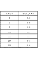
この形態例の場合、標準ピーク輝度は、ピーク輝度倍率SEL_PKで与える。ピーク輝度倍率SEL_PKは、基準ピーク輝度に対する倍率であり、事前に設定されるものとする。
この場合、あるフレームの消費電力は、平均階調値APL×ピーク輝度倍率SEL_PK×基準ピーク輝度で与えられる。
消費電力算出部151は、平均階調値APLに応じたピーク輝度倍率SEL_PKを、図9に示すルックアップテーブルを使用して読み出す。
In the case of this embodiment, the standard peak luminance is given by the peak luminance magnification SEL_PK. The peak luminance magnification SEL_PK is a magnification with respect to the reference peak luminance, and is set in advance.
In this case, power consumption of a certain frame is given by average gradation value APL × peak luminance magnification SEL_PK × reference peak luminance.
The power
図9に示すルックアップテーブルでは、平均階調値APLが小さいほど、ピーク輝度倍率SEL_PKを大きな値に設定する。図9では、2倍に設定する。これは平均階調値が低い画面内に高輝度領域が含まれる場合(例えば、夜空の映像に星が光る場合)にも十分なコントラストを確保するためである。
一方、図9に示すルックアップテーブルでは、平均階調値APLが大きいほど、ピーク輝度倍率SEL_PKを小さな値に設定する。
平均階調値APLに応じたピーク輝度倍率SEL_PKを以上の関係に定めることにより、画質を考慮した標準ピーク輝度が得られる。
In the lookup table shown in FIG. 9, the peak luminance magnification SEL_PK is set to a larger value as the average gradation value APL is smaller. In FIG. 9, it is set to double. This is to ensure sufficient contrast even when a high-luminance region is included in a screen with a low average gradation value (for example, when a star shines in a night sky image).
On the other hand, in the lookup table shown in FIG. 9, the peak luminance magnification SEL_PK is set to a smaller value as the average gradation value APL is larger.
By setting the peak luminance magnification SEL_PK corresponding to the average gradation value APL to the above relationship, the standard peak luminance considering the image quality can be obtained.
ピーク輝度調整部153は、一定期間内に消費される消費電力の合計値が設定電力量Smax を超えないように、先に算出した標準ピーク輝度を調整する処理デバイスである。何らの調整もしない場合、表示内容によっては設定電力量Smax を超えてしまうためである。
ピーク輝度調整部153は、基準期間(制御単位)内の残存期間で消費可能な実際の消費電力量(残存電力量)Aと、基準期間(制御単位)の全期間を同じピーク輝度で常時点灯する場合における残存期間での消費電力量Bとの比に応じて、対応フレームのピーク輝度を調整する。
The peak luminance adjustment unit 153 is a processing device that adjusts the previously calculated standard peak luminance so that the total value of power consumption consumed within a certain period does not exceed the set power amount Smax . This is because if no adjustment is made, the set power amount S max may be exceeded depending on the display content.
The peak luminance adjustment unit 153 is always lit with the same peak luminance for the actual power consumption (residual power amount) A that can be consumed in the remaining period within the reference period (control unit) and the entire period of the reference period (control unit). The peak luminance of the corresponding frame is adjusted in accordance with the ratio to the power consumption B during the remaining period in the case of doing.
具体的には、フレームnのピーク輝度倍率PKn を、(A/B)×標準ピーク輝度倍率SEL_PKn で与える。
ここで、実際の残存電力量Aは、(Sn-1
−APLn ×SEL_PKn )×基準ピーク輝度で与える。また、同一ピーク輝度で常時点灯する場合に消費可能な残存電力量Bは、((Tflat−n)×APLflat)×基準ピーク輝度で与える。
なお、Tflatは、基準期間に設定したフレーム数である。また、APLflatは、消費電力量を制限するためのAPL設定値(規定された消費電力を満たすように、基準期間の全期間を同じピーク輝度で点灯する場合におけるフレーム単位の平均階調値)である。
Specifically, the peak luminance magnification PK n of frame n is given by (A / B) × standard peak luminance magnification SEL_PK n .
Here, the actual remaining electric energy A is (S n-1
−APL n × SEL_PK n ) × reference peak luminance. Further, the remaining electric energy B that can be consumed when the lamp is always lit at the same peak luminance is given by ((T flat −n) × APL flat ) × reference peak luminance.
T flat is the number of frames set in the reference period. APL flat is an APL set value for limiting power consumption (an average gradation value in units of frames in the case where all reference periods are lit at the same peak luminance so as to satisfy specified power consumption). It is.
ところで、基準期間内に消費可能な残存電力量を与える初期値S0 (=Smax )は、Tflat×APLflat×PKflatで与える。PKflatは、APLflatに対応するピーク輝度倍率である。
また、nフレーム目をピーク輝度倍率PKn で点灯した場合における残存電力量A(=Sn )は、n−1フレーム目の残存電力量Sn-1 を用いることにより、Sn-1 −APLn ×PKn で与えられる。なお、計算上は基準ピーク輝度が省略されるため、ここでの電力量では、乗算すべき基準ピーク輝度の記載を省略している。
By the way, the initial value S 0 (= S max ) that gives the remaining electric energy that can be consumed within the reference period is given by T flat × APL flat × PK flat . PK flat is a peak luminance magnification corresponding to APL flat .
Further, the remaining power amount in the case of the n th frame illuminates the peak luminance magnification PK n A (= S n), by using the remaining power amount S n-1 of the n-1 th frame, S n-1 - APL n × PK n is given. In addition, since the reference peak luminance is omitted in the calculation, the reference peak luminance to be multiplied is omitted from the power amount here.
かかる制御により、入力映像信号の平均階調値に対応するピーク輝度倍率PKn は、以下のように調整される。
例えば、設定された消費電力を達成する平均階調値よりも明るいフレームが続く等により、実際の残存消費電力Aが全期間を平均的に点灯制御する際の残存電力量Bよりも小さくなっている場合には、調整後のピーク輝度倍率PKn は、本来の平均階調値に対応するピーク輝度倍率SEL_PKn よりも小さい値に制御される。
With this control, the peak luminance magnification PK n corresponding to the average gradation value of the input video signal is adjusted as follows.
For example, the actual remaining power consumption A becomes smaller than the remaining power amount B when the lighting control is averaged over the entire period because a frame that is brighter than the average gradation value that achieves the set power consumption continues. If so, the adjusted peak luminance magnification PK n is controlled to a value smaller than the peak luminance magnification SEL_PK n corresponding to the original average gradation value.
また例えば、設定された消費電力を達成する平均階調値よりも暗いフレームが続く等により、実際の残存消費電力Aが全期間を平均的に点灯制御する際の残存電力量Bよりも大きくなっている場合には、調整後のピーク輝度倍率PKn は、本来の平均階調値に対応するピーク輝度倍率SEL_PKn よりも大きい値に制御される。 Further, for example, the actual remaining power consumption A becomes larger than the remaining power amount B when the lighting control is averaged over the entire period because, for example, a frame that is darker than the average gradation value that achieves the set power consumption continues. In such a case, the adjusted peak luminance magnification PK n is controlled to a value larger than the peak luminance magnification SEL_PK n corresponding to the original average gradation value.
ピーク輝度制御部17と、消費電力量一定化制御部15から与えられるピーク輝度倍率PKn だけ、1フレーム内の点灯時間に相当する基準パルス幅をパルス幅変調し、得られたパルス幅の信号をデューティ比信号として出力する。以下、このデューティ比信号を「ピークコントロール信号」という。
なお、ピーク輝度制御部17は、入力映像信号の垂直同期信号Vsyncに同期したタイミングでピークコントロール信号を生成する。
The reference pulse width corresponding to the lighting time in one frame is subjected to pulse width modulation by a peak luminance magnification PK n given from the peak
The peak
フレーム遅延部19は、消費電力量一定化制御部15から出力されるピークコントロール信号と有機ELパネルに出力される映像信号の位相が一致するように映像信号を遅延するバッファメモリである。遅延時間は、任意である。
図10に、入出力フレームの位相関係を示す。図10(A)は、映像信号VSのフレーム番号(位相)を示す図である。図10(B)は、フレーム遅延部19に入力される画像データの番号(位相)を示す図である。
The
FIG. 10 shows the phase relationship between the input and output frames. FIG. 10A shows the frame number (phase) of the video signal VS. FIG. 10B is a diagram showing the number (phase) of image data input to the
図10(C)は、平均階調値算出部13より出力される平均階調値APLの番号(位相)を示す図である。図10(D)は、フレーム遅延部19から出力される画像データの番号(位相)を示す図である。図10(E)は、ピーク輝度制御部17から出力されるピークコントロール信号(位相)を示す図である。
図10(B)及び(D)を対比して分かるように、フレーム遅延部19では画像データが1フレーム分遅延されている。このため、図10(D)及び(E)に示すように、映像信号とピークコントロール信号の同期が確保される。
FIG. 10C is a diagram showing the number (phase) of the average gradation value APL output from the average gradation value calculation unit 13. FIG. 10D is a diagram illustrating the number (phase) of image data output from the
As can be seen by comparing FIGS. 10B and 10D, the
(b)ピーク輝度調整装置での処理動作の流れ
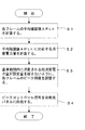
図11に、以上説明したピーク輝度調整装置11で実行される処理動作の概略を示す。
ピーク輝度調整装置11は、各フレームの平均階調値APLn を算出し(S1)、平均階調値に対応するピーク輝度倍率SEL_PKを求める。
この後、ピーク輝度調整装置11は、現フレームの平均階調値APLn とピーク輝度倍率SEL_PKとを用いて入力映像信号本来の消費電力量を算出する(S2)。
(B) Flow of processing operation in peak luminance adjusting device FIG. 11 shows an outline of processing operation executed in the peak
Peak
After that, the peak
次に、ピーク輝度調整装置11は、基準期間内に実際に消費される消費電力量が事前の設定量を超えないように、各フレームのピーク輝度(倍率)を調整する(S3)。
調整後のピーク輝度(倍率)に応じてパルス幅変調したピークコントロール信号を有機ELパネルモジュール1に出力する(S4)。
Next, the peak
A peak control signal that is pulse width modulated in accordance with the adjusted peak luminance (magnification) is output to the organic EL panel module 1 (S4).
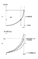
図12に、前述したピーク輝度制御機能の適用時における消費電力量の推移を示す。
いずれの基準期間(0−t0 、t1 −t2 、t2 −t3 …)についても、各基準期間で消費可能な設定電力量Smax 以下に抑制されていることが分かる。
なお、Sn (n=0、1、2…)は、各基準期間内での実際の消費電力量である。
FIG. 12 shows the transition of the power consumption when the above-described peak luminance control function is applied.
It can be seen that any reference period (0-t 0 , t 1 -t 2 , t 2 -t 3 ...) Is suppressed below the set power amount S max that can be consumed in each reference period.
S n (n = 0, 1, 2,...) Is an actual power consumption amount in each reference period.
(c)実現される効果
以上説明したピーク輝度調整装置をパネル基板上に搭載することにより、有機ELパネルの定消費電力化又は消費電力抑制化を実現できる。勿論、入力映像信号に応じたピーク輝度で点灯制御しても事前に設定した消費電力量を満たす場合には、入力映像信号を高い画質のまま表示することができる。
また、前述したピーク輝度の可変調整機能は、ソフトウェア処理で実現する場合にも演算負荷が小さく、集積回路で実現する場合にも非常に小規模な回路で実現することが可能であり、有機ELパネルモジュールへの実装に有利である。
(C) Effect Realized By mounting the above-described peak luminance adjusting device on the panel substrate, it is possible to realize constant power consumption or power consumption suppression of the organic EL panel. Of course, the input video signal can be displayed with high image quality if the preset power consumption is satisfied even if lighting control is performed with the peak luminance corresponding to the input video signal.
In addition, the above-described variable adjustment function of peak luminance has a small calculation load even when realized by software processing, and can be realized by a very small circuit even when realized by an integrated circuit. It is advantageous for mounting on a panel module.
(D)他の形態例
(a)前述の形態例では、発光時間の調整によりピーク輝度を可変制御する場合について説明したが、最大出力電圧の調整によりピーク輝度を可変制御しても良い。また、発光時間及び最大出力電圧の双方を同時に調整し、ピーク輝度を可変制御しても良い。
(b)前述の形態例では、算出された平均階調値APLに対応する標準ピーク輝度SEL_PKを、ルックアップテーブルから読み出す場合について説明したが、事前に設定した関係に従って算出しても良い。
(D) Other Embodiments (a) In the above embodiment, the case where the peak luminance is variably controlled by adjusting the light emission time has been described. However, the peak luminance may be variably controlled by adjusting the maximum output voltage. Further, both the light emission time and the maximum output voltage may be adjusted simultaneously to variably control the peak luminance.
(B) In the above-described embodiment, the case where the standard peak luminance SEL_PK corresponding to the calculated average gradation value APL is read from the lookup table has been described, but may be calculated according to a preset relationship.
(c)前述の形態例では、有機ELパネルモジュール1に最大出力電圧制御用ドライバ7Aと点灯時間制御用ゲートドライバ7Cを2つとも搭載するものとして説明した。
しかし、ピーク輝度の可変制御機能は、発光時間又は最大出力電圧のいずれか一方を可変制御することで実現できる。従って、発光時間を可変制御する方式を採用する場合には最大出力電圧制御用ドライバ7Aを搭載しない構成を採用し、最大出力電圧を可変制御する方式を採用する場合には点灯時間制御用ゲートドライバ7Cを搭載しない構成を採用しても良い。
(C) In the above-described embodiment, it has been described that the organic
However, the variable control function of peak luminance can be realized by variably controlling either the light emission time or the maximum output voltage. Therefore, when adopting a method for variably controlling the light emission time, a configuration without the maximum output
(d)前述の形態例においては、有機ELディスプレイパネルについて説明したが、無機ELディスプレイパネルにも応用できる。また例えば、FED(field emission display) 、無機ELディスプレイパネル、LEDパネル、PDP(Plasma Display
Panel)パネルその他の自発光パネルに適用できる。
(D) In the above-described embodiments, the organic EL display panel has been described, but the present invention can also be applied to an inorganic EL display panel. Also, for example, FED (field emission display), inorganic EL display panel, LED panel, PDP (Plasma Display)
Applicable to other self-luminous panels.
(e)前述の形態例においては、ピーク輝度調整装置11を有機ELディスプレイパネル上に実装する場合について説明した。
しかし、この有機ELディスプレイパネルその他の表示装置は、単独の商品形態でも良いし、他の画像処理装置の一部として搭載されても良い。
例えば、ビデオカメラ、デジタルカメラその他の撮像装置(カメラユニットだけでなく、記録装置と一体に構成されているものを含む。)、情報処理端末(携帯型のコンピュータ、携帯電話機、携帯型のゲーム機、電子手帳等)、ゲーム機の表示デバイスとしも実現できる。
特に、バッテリー駆動される電子機器に搭載する場合には、既存のバッテリー容量でより長時間の使用を達成できる。
(E) In the above-described embodiment, the case where the peak
However, this organic EL display panel and other display devices may be in the form of a single product or may be mounted as part of another image processing device.
For example, video cameras, digital cameras and other imaging devices (including not only camera units but also those integrated with a recording device), information processing terminals (portable computers, mobile phones, portable game machines) , Electronic notebook, etc.) and display devices for game machines.
In particular, when it is mounted on an electronic device driven by a battery, it can be used for a longer time with the existing battery capacity.
(f)前述の形態例では、ピーク輝度調整装置11を有機ELディスプレイパネル上に実装する場合について説明した。
しかし、ピーク輝度調整装置11は、有機ELディスプレイパネルその他の表示装置に対して入力映像信号を供給する画像処理装置側に搭載しても良い。この場合、画像処理装置から表示装置にデューティパルスや電圧値を供給する方式を採用しても良いし、これらの値を指示する情報を画像処理装置から表示装置に与える方式を採用しても良い。
(F) In the above-described embodiment, the case where the peak
However, the peak
(g)前述の形態例では、ピーク輝度調整装置11を機能構成の観点から説明したが、言うまでもなく、同等の機能をハードウェアとしてもソフトウェアとしても実現できる。
また、これらの処理機能の全てをハードウェア又はソフトウェアで実現するだけでなく、その一部はハードウェア又はソフトウェアを用いて実現しても良い。すなわち、ハードウェアとソフトウェアの組み合わせ構成としても良い。
(h)前述の形態例には、発明の趣旨の範囲内で様々な変形例が考えられる。また、本明細書の記載に基づいて創作される又は組み合わせられる各種の変形例及び応用例も考えられる。
(G) In the above-described embodiment, the peak
Further, not only all of these processing functions are realized by hardware or software, but some of them may be realized by using hardware or software. That is, a combination of hardware and software may be used.
(H) Various modifications can be considered for the above-described embodiments within the scope of the gist of the invention. Various modifications and applications created or combined based on the description of the present specification are also conceivable.
1 有機ELパネルモジュール
3A 発光領域
5 データドライバ
7A 電圧切替ドライバ7A
7B ゲートスキャンドライバ
7C 点灯時間制御用ゲートドライバ
9 タイミングジェネレータ
11 ピーク輝度調整装置
13 平均階調値算出部
15 消費電力量一定化制御部
151 消費電力算出部
153 ピーク輝度調整部
17 ピーク輝度制御部
19 フレーム遅延部
1 Organic EL Panel Module 3A
7B
Claims (6)
1フレーム期間中に入力される映像信号の平均階調値を算出する平均階調値算出部と、
算出された平均階調値に応じて、平均階調値との間に所定の負の相関がある標準ピーク輝度を求め、当該標準ピーク輝度と算出された平均階調値で消費される消費電力量を算出する消費電力算出部と、
一定期間内に消費される消費電力の合計値が設定電力量を超えないように、前記標準ピーク輝度を調整するピーク輝度調整部とを有しており、
前記ピーク輝度調整部は、調整後の標準ピーク輝度を、(A/B)×標準ピーク輝度で与える自発光表示装置。
ただし、Aは、制御単位に定めた一定期間内での残存期間に消費可能な実際の消費電力量であり、Bは、制御単位に定めた一定期間の全期間を同じピーク輝度で点灯する場合に残存期間に消費可能な消費電力量である。 In a self-luminous display device capable of variably controlling the peak luminance of the self-luminous panel surface in units of one frame,
An average gradation value calculating unit for calculating an average gradation value of a video signal input during one frame period;
In accordance with the calculated average gradation value, the standard peak luminance having a predetermined negative correlation with the average gradation value is obtained, and the power consumption consumed by the standard peak luminance and the calculated average gradation value A power consumption calculation unit for calculating the amount;
A peak luminance adjusting unit that adjusts the standard peak luminance so that the total value of power consumption consumed within a certain period does not exceed the set power amount ,
The peak luminance adjusting unit is a self-luminous display device that provides the adjusted standard peak luminance by (A / B) × standard peak luminance.
However, A is the actual power consumption that can be consumed during the remaining period within the fixed period determined in the control unit, and B is the case where the entire period of the fixed period determined in the control unit is lit with the same peak luminance. The amount of power that can be consumed during the remaining period.
算出された平均階調値に応じた標準ピーク輝度は、個々の平均階調値と標準ピーク輝度の組み合わせを記録した対応テーブルより読み出される自発光表示装置。The self-luminous display device in which the standard peak luminance corresponding to the calculated average gradation value is read from a correspondence table in which combinations of individual average gradation values and standard peak luminances are recorded.
1フレーム期間中に入力される映像信号の平均階調値を算出する平均階調値算出部と、An average gradation value calculating unit for calculating an average gradation value of a video signal input during one frame period;
算出された平均階調値に応じて、平均階調値との間に所定の負の相関がある標準ピーク輝度を求め、当該標準ピーク輝度と算出された平均階調値で消費される消費電力量を算出する消費電力算出部と、In accordance with the calculated average gradation value, the standard peak luminance having a predetermined negative correlation with the average gradation value is obtained, and the power consumption consumed by the standard peak luminance and the calculated average gradation value A power consumption calculation unit for calculating the amount;
一定期間内に消費される消費電力の合計値が設定電力量を超えないように、前記標準ピーク輝度を調整するピーク輝度調整部とを有しており、A peak luminance adjusting unit that adjusts the standard peak luminance so that the total value of power consumption consumed within a certain period does not exceed the set power amount,
前記ピーク輝度調整部は、調整後の標準ピーク輝度を、(A/B)×標準ピーク輝度で与えるピーク輝度調整装置。The peak luminance adjusting unit is a peak luminance adjusting device that gives the adjusted standard peak luminance by (A / B) × standard peak luminance.
ただし、Aは、制御単位に定めた一定期間内での残存期間に消費可能な実際の消費電力量であり、Bは、制御単位に定めた一定期間の全期間を同じピーク輝度で点灯する場合に残存期間に消費可能な消費電力量である。However, A is the actual power consumption that can be consumed during the remaining period within the fixed period determined in the control unit, and B is the case where the entire period of the fixed period determined in the control unit is lit with the same peak luminance. The amount of power that can be consumed during the remaining period.
1フレーム期間中に入力される映像信号の平均階調値を算出する平均階調値算出部と、An average gradation value calculating unit for calculating an average gradation value of a video signal input during one frame period;
算出された平均階調値に応じて、平均階調値との間に所定の負の相関がある標準ピーク輝度を求め、当該標準ピーク輝度と算出された平均階調値で消費される消費電力量を算出する消費電力算出部と、In accordance with the calculated average gradation value, the standard peak luminance having a predetermined negative correlation with the average gradation value is obtained, and the power consumption consumed by the standard peak luminance and the calculated average gradation value A power consumption calculation unit for calculating the amount;
一定期間内に消費される消費電力の合計値が設定電力量を超えないように、前記標準ピーク輝度を調整するピーク輝度調整部とを有しており、A peak luminance adjusting unit that adjusts the standard peak luminance so that the total value of power consumption consumed within a certain period does not exceed the set power amount,
前記ピーク輝度調整部は、調整後の標準ピーク輝度を、(A/B)×標準ピーク輝度で与える電子機器。The peak luminance adjustment unit is an electronic device that gives the adjusted standard peak luminance by (A / B) × standard peak luminance.
ただし、Aは、制御単位に定めた一定期間内での残存期間に消費可能な実際の消費電力量であり、Bは、制御単位に定めた一定期間の全期間を同じピーク輝度で点灯する場合に残存期間に消費可能な消費電力量である。However, A is the actual power consumption that can be consumed during the remaining period within the fixed period determined in the control unit, and B is the case where the entire period of the fixed period determined in the control unit is lit with the same peak luminance. The amount of power that can be consumed during the remaining period.
1フレーム期間中に入力される映像信号の平均階調値を算出する処理と、A process of calculating an average gradation value of a video signal input during one frame period;
算出された平均階調値に応じて、平均階調値との間に所定の負の相関がある標準ピーク輝度を求め、当該標準ピーク輝度と算出された平均階調値で消費される消費電力量を算出する処理と、In accordance with the calculated average gradation value, the standard peak luminance having a predetermined negative correlation with the average gradation value is obtained, and the power consumption consumed by the standard peak luminance and the calculated average gradation value Processing to calculate the amount;
一定期間内に消費される消費電力の合計値が設定電力量を超えないように、前記標準ピーク輝度を調整する処理とA process of adjusting the standard peak luminance so that the total value of power consumed within a certain period does not exceed the set power amount;
を有しており、Have
前記標準ピーク輝度を調整する処理は、調整後の標準ピーク輝度を、(A/B)×標準ピーク輝度で与えるピーク輝度調整方法。The process of adjusting the standard peak luminance is a peak luminance adjustment method in which the adjusted standard peak luminance is given by (A / B) × standard peak luminance.
ただし、Aは、制御単位に定めた一定期間内での残存期間に消費可能な実際の消費電力量であり、Bは、制御単位に定めた一定期間の全期間を同じピーク輝度で点灯する場合に残存期間に消費可能な消費電力量である。However, A is the actual power consumption that can be consumed during the remaining period within the fixed period determined in the control unit, and B is the case where the entire period of the fixed period determined in the control unit is lit with the same peak luminance. The amount of power that can be consumed during the remaining period.
1フレーム期間中に入力される映像信号の平均階調値を算出する処理と、A process of calculating an average gradation value of a video signal input during one frame period;
算出された平均階調値に応じて、平均階調値との間に所定の負の相関がある標準ピーク輝度を求め、当該標準ピーク輝度と算出された平均階調値で消費される消費電力量を算出する処理と、In accordance with the calculated average gradation value, the standard peak luminance having a predetermined negative correlation with the average gradation value is obtained, and the power consumption consumed by the standard peak luminance and the calculated average gradation value Processing to calculate the amount;
一定期間内に消費される消費電力の合計値が設定電力量を超えないように、前記標準ピーク輝度を調整する処理とを実行させるコンピュータプログラムにおいて、In a computer program for executing the process of adjusting the standard peak luminance so that the total value of power consumption consumed within a certain period does not exceed a set power amount,
前記標準ピーク輝度を調整する処理は、調整後の標準ピーク輝度を、(A/B)×標準ピーク輝度で与えるコンピュータプログラム。The process of adjusting the standard peak luminance is a computer program that gives the adjusted standard peak luminance by (A / B) × standard peak luminance.
ただし、Aは、制御単位に定めた一定期間内での残存期間に消費可能な実際の消費電力量であり、Bは、制御単位に定めた一定期間の全期間を同じピーク輝度で点灯する場合に残存期間に消費可能な消費電力量である。However, A is the actual power consumption that can be consumed during the remaining period within the fixed period determined in the control unit, and B is the case where the entire period of the fixed period determined in the control unit is lit with the same peak luminance. The amount of power that can be consumed during the remaining period.
Priority Applications (6)
| Application Number | Priority Date | Filing Date | Title |
|---|---|---|---|
| JP2005340436A JP4862369B2 (en) | 2005-11-25 | 2005-11-25 | Self-luminous display device, peak luminance adjusting device, electronic device, peak luminance adjusting method and program |
| TW095143031A TW200733045A (en) | 2005-11-25 | 2006-11-21 | Self light-emitting display apparatus, peak brightness adjustment apparatus, electronic machine, peak brightness adjustment method and program |
| US11/603,215 US8325115B2 (en) | 2005-11-25 | 2006-11-22 | Self-luminous display apparatus, peak luminance adjustment apparatus, electronic apparatus, peak luminance adjustment method and program |
| KR1020060116312A KR101367916B1 (en) | 2005-11-25 | 2006-11-23 | Self light emission display device, peak luminance control device, electronic apparatus, peak luminance control method and program |
| CNB2006100644574A CN100524399C (en) | 2005-11-25 | 2006-11-24 | Display device, electronic apparatus, peak luminance control method and program |
| US13/657,388 US9214108B2 (en) | 2005-11-25 | 2012-10-22 | Self-luminous display apparatus, peak luminance adjustment apparatus, electronic apparatus, peak luminance adjustment method and program |
Applications Claiming Priority (1)
| Application Number | Priority Date | Filing Date | Title |
|---|---|---|---|
| JP2005340436A JP4862369B2 (en) | 2005-11-25 | 2005-11-25 | Self-luminous display device, peak luminance adjusting device, electronic device, peak luminance adjusting method and program |
Publications (2)
| Publication Number | Publication Date |
|---|---|
| JP2007147868A JP2007147868A (en) | 2007-06-14 |
| JP4862369B2 true JP4862369B2 (en) | 2012-01-25 |
Family
ID=38118179
Family Applications (1)
| Application Number | Title | Priority Date | Filing Date |
|---|---|---|---|
| JP2005340436A Active JP4862369B2 (en) | 2005-11-25 | 2005-11-25 | Self-luminous display device, peak luminance adjusting device, electronic device, peak luminance adjusting method and program |
Country Status (5)
| Country | Link |
|---|---|
| US (2) | US8325115B2 (en) |
| JP (1) | JP4862369B2 (en) |
| KR (1) | KR101367916B1 (en) |
| CN (1) | CN100524399C (en) |
| TW (1) | TW200733045A (en) |
Families Citing this family (67)
| Publication number | Priority date | Publication date | Assignee | Title |
|---|---|---|---|---|
| CA2443206A1 (en) | 2003-09-23 | 2005-03-23 | Ignis Innovation Inc. | Amoled display backplanes - pixel driver circuits, array architecture, and external compensation |
| US10012678B2 (en) | 2004-12-15 | 2018-07-03 | Ignis Innovation Inc. | Method and system for programming, calibrating and/or compensating, and driving an LED display |
| TWI402790B (en) | 2004-12-15 | 2013-07-21 | Ignis Innovation Inc | Method and system for programming, calibrating and driving a light emitting device display |
| US20140111567A1 (en) * | 2005-04-12 | 2014-04-24 | Ignis Innovation Inc. | System and method for compensation of non-uniformities in light emitting device displays |
| US8576217B2 (en) | 2011-05-20 | 2013-11-05 | Ignis Innovation Inc. | System and methods for extraction of threshold and mobility parameters in AMOLED displays |
| US10013907B2 (en) * | 2004-12-15 | 2018-07-03 | Ignis Innovation Inc. | Method and system for programming, calibrating and/or compensating, and driving an LED display |
| US9799246B2 (en) | 2011-05-20 | 2017-10-24 | Ignis Innovation Inc. | System and methods for extraction of threshold and mobility parameters in AMOLED displays |
| JP5355080B2 (en) | 2005-06-08 | 2013-11-27 | イグニス・イノベイション・インコーポレーテッド | Method and system for driving a light emitting device display |
| TW200746022A (en) | 2006-04-19 | 2007-12-16 | Ignis Innovation Inc | Stable driving scheme for active matrix displays |
| JP2007322718A (en) * | 2006-05-31 | 2007-12-13 | Sanyo Electric Co Ltd | Display apparatus |
| CA2556961A1 (en) | 2006-08-15 | 2008-02-15 | Ignis Innovation Inc. | Oled compensation technique based on oled capacitance |
| JP2008252185A (en) * | 2007-03-29 | 2008-10-16 | Kyocera Corp | Portable electronic apparatus |
| JP5034805B2 (en) * | 2007-09-13 | 2012-09-26 | ソニー株式会社 | Display device and display driving method |
| JP5176522B2 (en) * | 2007-12-13 | 2013-04-03 | ソニー株式会社 | Self-luminous display device and driving method thereof |
| JP5211732B2 (en) * | 2008-02-14 | 2013-06-12 | ソニー株式会社 | Lighting period setting method, display panel driving method, lighting condition setting device, semiconductor device, display panel, and electronic apparatus |
| JP5091796B2 (en) * | 2008-08-05 | 2012-12-05 | 株式会社東芝 | Image processing device |
| RU2496155C2 (en) * | 2008-10-10 | 2013-10-20 | Шарп Кабусики Кайся | Power control method for light-emitting device for image display, light-emitting device for image display, display device and television receiver |
| JP5321032B2 (en) | 2008-12-11 | 2013-10-23 | ソニー株式会社 | Display device, brightness adjusting device, brightness adjusting method and program |
| JP5304211B2 (en) | 2008-12-11 | 2013-10-02 | ソニー株式会社 | Display device, brightness adjusting device, backlight device, brightness adjusting method and program |
| JP2011002520A (en) * | 2009-06-16 | 2011-01-06 | Sony Corp | Self-luminous display device, power consumption reduction method, and program |
| CA2669367A1 (en) | 2009-06-16 | 2010-12-16 | Ignis Innovation Inc | Compensation technique for color shift in displays |
| US10319307B2 (en) | 2009-06-16 | 2019-06-11 | Ignis Innovation Inc. | Display system with compensation techniques and/or shared level resources |
| US9384698B2 (en) | 2009-11-30 | 2016-07-05 | Ignis Innovation Inc. | System and methods for aging compensation in AMOLED displays |
| US9311859B2 (en) | 2009-11-30 | 2016-04-12 | Ignis Innovation Inc. | Resetting cycle for aging compensation in AMOLED displays |
| KR101658138B1 (en) * | 2009-10-07 | 2016-09-21 | 엘지디스플레이 주식회사 | Driving appratus of organic light emitting diode display device and method for driving the same |
| CA2692097A1 (en) | 2010-02-04 | 2011-08-04 | Ignis Innovation Inc. | Extracting correlation curves for light emitting device |
| US10089921B2 (en) | 2010-02-04 | 2018-10-02 | Ignis Innovation Inc. | System and methods for extracting correlation curves for an organic light emitting device |
| US20140313111A1 (en) | 2010-02-04 | 2014-10-23 | Ignis Innovation Inc. | System and methods for extracting correlation curves for an organic light emitting device |
| US9881532B2 (en) | 2010-02-04 | 2018-01-30 | Ignis Innovation Inc. | System and method for extracting correlation curves for an organic light emitting device |
| US8907991B2 (en) | 2010-12-02 | 2014-12-09 | Ignis Innovation Inc. | System and methods for thermal compensation in AMOLED displays |
| US9530349B2 (en) | 2011-05-20 | 2016-12-27 | Ignis Innovations Inc. | Charged-based compensation and parameter extraction in AMOLED displays |
| US9466240B2 (en) | 2011-05-26 | 2016-10-11 | Ignis Innovation Inc. | Adaptive feedback system for compensating for aging pixel areas with enhanced estimation speed |
| JP2014517940A (en) | 2011-05-27 | 2014-07-24 | イグニス・イノベイション・インコーポレーテッド | System and method for aging compensation in AMOLED displays |
| KR101492682B1 (en) * | 2011-09-23 | 2015-02-13 | 엘지디스플레이 주식회사 | Organic Light Emitting Display Device and Driving Method thereof |
| US10089924B2 (en) | 2011-11-29 | 2018-10-02 | Ignis Innovation Inc. | Structural and low-frequency non-uniformity compensation |
| US9324268B2 (en) | 2013-03-15 | 2016-04-26 | Ignis Innovation Inc. | Amoled displays with multiple readout circuits |
| US8937632B2 (en) | 2012-02-03 | 2015-01-20 | Ignis Innovation Inc. | Driving system for active-matrix displays |
| JP2013228560A (en) * | 2012-04-25 | 2013-11-07 | Sharp Corp | Light-emitting diode control circuit and display device |
| US8922544B2 (en) | 2012-05-23 | 2014-12-30 | Ignis Innovation Inc. | Display systems with compensation for line propagation delay |
| KR101937937B1 (en) * | 2012-10-12 | 2019-04-11 | 엘지디스플레이 주식회사 | Peak Luminance Control Unit And Organic Light Emitting Diode Display Device Including The Same |
| KR101456958B1 (en) * | 2012-10-15 | 2014-10-31 | 엘지디스플레이 주식회사 | Apparatus and method for driving of organic light emitting display device |
| KR101992904B1 (en) * | 2012-12-21 | 2019-06-26 | 엘지디스플레이 주식회사 | Organic light emitting diode display device and driving method the same |
| JP5957675B2 (en) | 2012-12-21 | 2016-07-27 | 株式会社Joled | Self-luminous display device, self-luminous display device control method, and computer program |
| EP3043338A1 (en) | 2013-03-14 | 2016-07-13 | Ignis Innovation Inc. | Re-interpolation with edge detection for extracting an aging pattern for amoled displays |
| US9368067B2 (en) | 2013-05-14 | 2016-06-14 | Apple Inc. | Organic light-emitting diode display with dynamic power supply control |
| JP6274771B2 (en) * | 2013-07-26 | 2018-02-07 | 株式会社ジャパンディスプレイ | Light emitting element display device |
| KR102074719B1 (en) | 2013-10-08 | 2020-02-07 | 엘지디스플레이 주식회사 | Organic light emitting display device |
| CN103531155B (en) * | 2013-10-09 | 2016-01-20 | 广东欧珀移动通信有限公司 | Mobile device with recording function reduces method and the device of power consumption when recording a video |
| US9396684B2 (en) | 2013-11-06 | 2016-07-19 | Apple Inc. | Display with peak luminance control sensitive to brightness setting |
| CN104332151B (en) * | 2013-11-06 | 2017-04-12 | 苹果公司 | Display device, display device circuit and method for operating display device |
| JP2015099181A (en) * | 2013-11-18 | 2015-05-28 | 株式会社ジャパンディスプレイ | Display device |
| US9741282B2 (en) | 2013-12-06 | 2017-08-22 | Ignis Innovation Inc. | OLED display system and method |
| US9761170B2 (en) | 2013-12-06 | 2017-09-12 | Ignis Innovation Inc. | Correction for localized phenomena in an image array |
| US9502653B2 (en) | 2013-12-25 | 2016-11-22 | Ignis Innovation Inc. | Electrode contacts |
| DE102015206281A1 (en) | 2014-04-08 | 2015-10-08 | Ignis Innovation Inc. | Display system with shared level resources for portable devices |
| JP6343515B2 (en) * | 2014-07-31 | 2018-06-13 | 株式会社ジャパンディスプレイ | Display device |
| KR102242761B1 (en) * | 2014-10-23 | 2021-04-21 | 엘지디스플레이 주식회사 | Apparatus for converting data and display apparatus |
| CA2879462A1 (en) | 2015-01-23 | 2016-07-23 | Ignis Innovation Inc. | Compensation for color variation in emissive devices |
| CA2889870A1 (en) | 2015-05-04 | 2016-11-04 | Ignis Innovation Inc. | Optical feedback system |
| CA2892714A1 (en) | 2015-05-27 | 2016-11-27 | Ignis Innovation Inc | Memory bandwidth reduction in compensation system |
| KR102473208B1 (en) * | 2015-07-06 | 2022-12-05 | 삼성디스플레이 주식회사 | Organic light emitting display device and driving method thereof |
| CA2900170A1 (en) | 2015-08-07 | 2017-02-07 | Gholamreza Chaji | Calibration of pixel based on improved reference values |
| JP2017076007A (en) * | 2015-10-13 | 2017-04-20 | 株式会社ジャパンディスプレイ | Control device and display device |
| KR20170049735A (en) | 2015-10-28 | 2017-05-11 | 삼성디스플레이 주식회사 | Display device |
| KR101884233B1 (en) * | 2016-08-26 | 2018-08-01 | 삼성전자주식회사 | Display apparatus and driving method thereof |
| US10181278B2 (en) | 2016-09-06 | 2019-01-15 | Microsoft Technology Licensing, Llc | Display diode relative age |
| JP2019168501A (en) * | 2018-03-22 | 2019-10-03 | キヤノン株式会社 | Display controller and display control method |
Family Cites Families (23)
| Publication number | Priority date | Publication date | Assignee | Title |
|---|---|---|---|---|
| JP2994630B2 (en) * | 1997-12-10 | 1999-12-27 | 松下電器産業株式会社 | Display device capable of adjusting the number of subfields by brightness |
| JP3544855B2 (en) * | 1998-03-26 | 2004-07-21 | 富士通株式会社 | Display unit power consumption control method and device, display system including the device, and storage medium storing program for implementing the method |
| EP1031131B1 (en) * | 1998-09-18 | 2010-10-27 | Panasonic Corporation | Colour display apparatus |
| JP3242641B1 (en) * | 1998-09-18 | 2001-12-25 | 松下電器産業株式会社 | Plasma display |
| JP3811738B2 (en) * | 1998-12-24 | 2006-08-23 | 株式会社日立プラズマパテントライセンシング | Display device |
| JP2000276091A (en) * | 1999-03-24 | 2000-10-06 | Canon Inc | Flat panel type display device and its controlling method |
| JP2001343941A (en) | 2000-05-30 | 2001-12-14 | Hitachi Ltd | Display device |
| JP2001346219A (en) * | 2000-05-31 | 2001-12-14 | Fujitsu General Ltd | Projection method and projector |
| JP2002132218A (en) | 2000-10-26 | 2002-05-09 | Sony Corp | Display device, brightness limiting circuit, and method for driving the display device |
| JP2003015605A (en) | 2001-07-03 | 2003-01-17 | Sony Corp | Active matrix type display device, active matrix type organic electro-luiminescence display device, and driving method therefor |
| EP1345428A3 (en) * | 2002-03-11 | 2005-03-16 | Sony Corporation | Optical intensity modulation method and system, and optical state modulation apparatus |
| JP3922090B2 (en) * | 2002-05-17 | 2007-05-30 | 株式会社日立製作所 | Display device and display control method |
| JP3674606B2 (en) * | 2002-06-11 | 2005-07-20 | ソニー株式会社 | Light quantity modulation device, display system, and light quantity modulation method |
| US20050062696A1 (en) * | 2003-09-24 | 2005-03-24 | Shin-Tai Lo | Driving apparatus and method of a display device for automatically adjusting the optimum brightness under limited power consumption |
| US20050123193A1 (en) * | 2003-12-05 | 2005-06-09 | Nokia Corporation | Image adjustment with tone rendering curve |
| JP4519493B2 (en) * | 2004-03-25 | 2010-08-04 | パナソニック株式会社 | Display device |
| EP1622119A1 (en) * | 2004-07-29 | 2006-02-01 | Deutsche Thomson-Brandt Gmbh | Method and apparatus for power level control and/or contrast control of a display device |
| WO2006025359A1 (en) * | 2004-09-03 | 2006-03-09 | Sharp Kabushiki Kaisha | Display driving method, display driving device, its program and recording medium, and display |
| JP4403401B2 (en) * | 2004-10-13 | 2010-01-27 | ソニー株式会社 | Information processing apparatus and method, recording medium, and program |
| US7880815B2 (en) * | 2005-01-10 | 2011-02-01 | Mavs Lab, Inc. | Method for detecting and eliminating flash scene in digital video |
| JP2006201399A (en) * | 2005-01-19 | 2006-08-03 | Fuji Photo Film Co Ltd | Display device and display control method |
| US7236845B2 (en) * | 2005-03-10 | 2007-06-26 | Eastman Kodak Company | Selecting OLED devices using figure of merit |
| US8847972B2 (en) * | 2010-01-20 | 2014-09-30 | Intellectual Ventures Fund 83 Llc | Adapting display color for low luminance conditions |
-
2005
- 2005-11-25 JP JP2005340436A patent/JP4862369B2/en active Active
-
2006
- 2006-11-21 TW TW095143031A patent/TW200733045A/en unknown
- 2006-11-22 US US11/603,215 patent/US8325115B2/en active Active
- 2006-11-23 KR KR1020060116312A patent/KR101367916B1/en active IP Right Grant
- 2006-11-24 CN CNB2006100644574A patent/CN100524399C/en active Active
-
2012
- 2012-10-22 US US13/657,388 patent/US9214108B2/en active Active
Also Published As
| Publication number | Publication date |
|---|---|
| TW200733045A (en) | 2007-09-01 |
| US20130050295A1 (en) | 2013-02-28 |
| US8325115B2 (en) | 2012-12-04 |
| US9214108B2 (en) | 2015-12-15 |
| CN100524399C (en) | 2009-08-05 |
| JP2007147868A (en) | 2007-06-14 |
| KR101367916B1 (en) | 2014-02-27 |
| US20070126672A1 (en) | 2007-06-07 |
| TWI357050B (en) | 2012-01-21 |
| KR20070055374A (en) | 2007-05-30 |
| CN101030346A (en) | 2007-09-05 |
Similar Documents
| Publication | Publication Date | Title |
|---|---|---|
| JP4862369B2 (en) | Self-luminous display device, peak luminance adjusting device, electronic device, peak luminance adjusting method and program | |
| JP4036142B2 (en) | Electro-optical device, driving method of electro-optical device, and electronic apparatus | |
| KR101425889B1 (en) | Peak intensity level control device, self light-emitting display device, electronic device, peak intensity level control method, and computer program | |
| JP2008026395A (en) | Power consumption detection device and method, power consumption controller, image processor, self-luminous light emitting display device, electronic equipment, power consumption control method, and computer program | |
| KR100782456B1 (en) | Driving Method of Organic Electro Luminescence Display Device | |
| JP4952972B2 (en) | Self-luminous display device, light emission condition optimization device, light emission condition optimization method and program | |
| JP2008026761A (en) | Power consumption controller and control method, image processor, self-luminous light emitting display device, electronic equipment, and computer program | |
| JP4899447B2 (en) | Self-luminous display device, light emission condition control device, light emission condition control method, and program | |
| JP5082319B2 (en) | Light emission condition control device, image processing device, self light emission display device, electronic device, light emission condition control method, and computer program | |
| JPWO2003081567A1 (en) | Display device, portable terminal, and luminance control method in portable terminal | |
| EP3767616A1 (en) | Display apparatus and method of driving display panel using the same | |
| JP2007147867A (en) | Self emitting display device, light emitting condition controller, light emitting condition control method, and program | |
| JP2008089956A (en) | Power consumption information calculating device, power consumption controller, image processor, spontaneous light emitting display device, electronic apparatus, power consumption information calculating method, power consumption control method, and computer program | |
| JP2008292866A (en) | Cathode potential control device, self-luminous display device, electronic equipment and cathode potential control method | |
| JP2006284974A (en) | In-plane temperature adjusting method, display apparatus, in-plane temperature adjusting apparatus and program | |
| JP5310811B2 (en) | Temperature unevenness correction amount determination method, display device, temperature unevenness correction amount determination device, temperature unevenness correction device, and program | |
| JP5092201B2 (en) | Temperature unevenness correction amount determination method, display device, temperature unevenness correction amount determination device, temperature unevenness correction device, and program | |
| TWI293749B (en) | Method and structure for increasing gray scale uniformity of oled | |
| US20110043544A1 (en) | Image display device | |
| JP2008292867A (en) | Contrast control device, self-luminous display device, electronic equipment and contrast control method | |
| JP2009063654A (en) | Display device and drive method thereof | |
| JP2012098342A (en) | Light-emission element display device |
Legal Events
| Date | Code | Title | Description |
|---|---|---|---|
| A621 | Written request for application examination |
Free format text: JAPANESE INTERMEDIATE CODE: A621 Effective date: 20081106 |
|
| RD02 | Notification of acceptance of power of attorney |
Free format text: JAPANESE INTERMEDIATE CODE: A7422 Effective date: 20081219 |
|
| RD04 | Notification of resignation of power of attorney |
Free format text: JAPANESE INTERMEDIATE CODE: A7424 Effective date: 20081225 |
|
| A521 | Request for written amendment filed |
Free format text: JAPANESE INTERMEDIATE CODE: A821 Effective date: 20091009 |
|
| RD02 | Notification of acceptance of power of attorney |
Free format text: JAPANESE INTERMEDIATE CODE: A7422 Effective date: 20091009 |
|
| RD04 | Notification of resignation of power of attorney |
Free format text: JAPANESE INTERMEDIATE CODE: A7424 Effective date: 20091105 |
|
| A131 | Notification of reasons for refusal |
Free format text: JAPANESE INTERMEDIATE CODE: A131 Effective date: 20110802 |
|
| A521 | Request for written amendment filed |
Free format text: JAPANESE INTERMEDIATE CODE: A523 Effective date: 20110913 |
|
| TRDD | Decision of grant or rejection written | ||
| A01 | Written decision to grant a patent or to grant a registration (utility model) |
Free format text: JAPANESE INTERMEDIATE CODE: A01 Effective date: 20111011 |
|
| A01 | Written decision to grant a patent or to grant a registration (utility model) |
Free format text: JAPANESE INTERMEDIATE CODE: A01 |
|
| A61 | First payment of annual fees (during grant procedure) |
Free format text: JAPANESE INTERMEDIATE CODE: A61 Effective date: 20111024 |
|
| FPAY | Renewal fee payment (event date is renewal date of database) |
Free format text: PAYMENT UNTIL: 20141118 Year of fee payment: 3 |
|
| R151 | Written notification of patent or utility model registration |
Ref document number: 4862369 Country of ref document: JP Free format text: JAPANESE INTERMEDIATE CODE: R151 |
|
| FPAY | Renewal fee payment (event date is renewal date of database) |
Free format text: PAYMENT UNTIL: 20141118 Year of fee payment: 3 |
|
| R250 | Receipt of annual fees |
Free format text: JAPANESE INTERMEDIATE CODE: R250 |
|
| S111 | Request for change of ownership or part of ownership |
Free format text: JAPANESE INTERMEDIATE CODE: R313111 |
|
| R350 | Written notification of registration of transfer |
Free format text: JAPANESE INTERMEDIATE CODE: R350 |
|
| R250 | Receipt of annual fees |
Free format text: JAPANESE INTERMEDIATE CODE: R250 |
|
| R250 | Receipt of annual fees |
Free format text: JAPANESE INTERMEDIATE CODE: R250 |
|
| R250 | Receipt of annual fees |
Free format text: JAPANESE INTERMEDIATE CODE: R250 |
|
| R250 | Receipt of annual fees |
Free format text: JAPANESE INTERMEDIATE CODE: R250 |
|
| R250 | Receipt of annual fees |
Free format text: JAPANESE INTERMEDIATE CODE: R250 |
|
| R250 | Receipt of annual fees |
Free format text: JAPANESE INTERMEDIATE CODE: R250 |
|
| R250 | Receipt of annual fees |
Free format text: JAPANESE INTERMEDIATE CODE: R250 |
|
| R250 | Receipt of annual fees |
Free format text: JAPANESE INTERMEDIATE CODE: R250 |
|
| R250 | Receipt of annual fees |
Free format text: JAPANESE INTERMEDIATE CODE: R250 |
|
| S303 | Written request for registration of pledge or change of pledge |
Free format text: JAPANESE INTERMEDIATE CODE: R316303 |
|
| R350 | Written notification of registration of transfer |
Free format text: JAPANESE INTERMEDIATE CODE: R350 |
|
| S803 | Written request for registration of cancellation of provisional registration |
Free format text: JAPANESE INTERMEDIATE CODE: R316803 |
|
| R350 | Written notification of registration of transfer |
Free format text: JAPANESE INTERMEDIATE CODE: R350 |
|
| R250 | Receipt of annual fees |
Free format text: JAPANESE INTERMEDIATE CODE: R250 |
|
| S111 | Request for change of ownership or part of ownership |
Free format text: JAPANESE INTERMEDIATE CODE: R313113 |