JP4850168B2 - Semiconductor device - Google Patents
Semiconductor device Download PDFInfo
- Publication number
- JP4850168B2 JP4850168B2 JP2007315900A JP2007315900A JP4850168B2 JP 4850168 B2 JP4850168 B2 JP 4850168B2 JP 2007315900 A JP2007315900 A JP 2007315900A JP 2007315900 A JP2007315900 A JP 2007315900A JP 4850168 B2 JP4850168 B2 JP 4850168B2
- Authority
- JP
- Japan
- Prior art keywords
- wiring
- film
- amorphous semiconductor
- metal
- insulating film
- Prior art date
- Legal status (The legal status is an assumption and is not a legal conclusion. Google has not performed a legal analysis and makes no representation as to the accuracy of the status listed.)
- Expired - Fee Related
Links
Images


Landscapes
- Liquid Crystal (AREA)
- Electrodes Of Semiconductors (AREA)
- Devices For Indicating Variable Information By Combining Individual Elements (AREA)
- Internal Circuitry In Semiconductor Integrated Circuit Devices (AREA)
- Thin Film Transistor (AREA)
Description
本発明は薄膜トランジスタ(以下、TFTという)で構成された半導体回路を有する半導体装置及びその作製方法に係わり、特に液晶表示パネルに代表される電気光学装置及び前記電気光学装置を部品として搭載した電子機器に関する技術である。 The present invention relates to a semiconductor device having a semiconductor circuit composed of a thin film transistor (hereinafter referred to as TFT) and a manufacturing method thereof, and more particularly to an electro-optical device typified by a liquid crystal display panel and an electronic apparatus in which the electro-optical device is mounted as a component. Technology.
なお、本明細書中において半導体装置とは半導体特性を利用することで機能しうる装置全般を指し、電気光学装置(以下、表示装置と記す)、半導体回路及び電子機器は全て半導体装置である。 Note that in this specification, a semiconductor device refers to all devices that can function by utilizing semiconductor characteristics, and an electro-optical device (hereinafter referred to as a display device), a semiconductor circuit, and an electronic device are all semiconductor devices.
近年、絶縁表面を有する基板上に形成された半導体薄膜(厚さ数百〜数千nm程度)を用いてTFTを作製する技術が開発されている。TFTは集積回路(Integrated Circuit;IC)や電気光学装置のような半導体装置に広く応用され、特に表示装置などのスイッチング素子として開発が急がれている。 In recent years, a technique for manufacturing a TFT using a semiconductor thin film (having a thickness of about several hundred to several thousand nm) formed on a substrate having an insulating surface has been developed. TFTs are widely applied to semiconductor devices such as integrated circuits (ICs) and electro-optical devices, and development of switching devices such as display devices is urgently required.
半導体装置は、パッシブ型の液晶表示装置と比較して高精細な画像が得られることから、アクティブマトリックス型の液晶表示装置が多く用いられている。そして、アクティブマトリックス液晶表示装置はゲート配線と、ソース配線と、前記ゲート線と前記ソース線の交差に設けた画素部のTFTと、前記画素部のTFTに接続する画素電極とを有している。従来のアクティブマトリックス液晶表示装置のゲート配線はTi/Al/Tiの3層構造になっており、また従来のアクティブマトリックス液晶表示装置のソース配線はTaN/Wの2層構造になっている。前記ソース配線材料のTaN/Wは熱処理に耐えうる金属材料で、配線抵抗がAl等と比較するとやや高くなっている。 As a semiconductor device, an active matrix liquid crystal display device is often used because a high-definition image can be obtained as compared with a passive liquid crystal display device. The active matrix liquid crystal display device includes a gate line, a source line, a TFT of a pixel portion provided at an intersection of the gate line and the source line, and a pixel electrode connected to the TFT of the pixel portion. . The gate wiring of the conventional active matrix liquid crystal display device has a three-layer structure of Ti / Al / Ti, and the source wiring of the conventional active matrix liquid crystal display device has a two-layer structure of TaN / W. TaN / W of the source wiring material is a metal material that can withstand heat treatment, and its wiring resistance is slightly higher than that of Al or the like.
このような構造を有する従来のアクティブマトリックス液晶表示装置は、モニターやテレビさらに携帯端末の表示装置として用途が拡大しているとともに量産化が進んでいる。更に、画面サイズの大面積化、高精細化、高開口率化、高信頼性の要求が高まっている。 The conventional active matrix liquid crystal display device having such a structure has been used as a display device for a monitor, a television, and a portable terminal, and has been mass-produced. Furthermore, demands for larger screen sizes, higher definition, higher aperture ratios, and higher reliability are increasing.
従来の5インチ程度の画面サイズの半導体装置ならば、半導体表示装置の配線抵抗は問題にならなかった。しかし、画面サイズが大画面化するとゲート配線とソース配線の長さが増加して、特にTaN/Wの金属材料でできているソース配線の配線抵抗が高くなる問題が発生し、消費電力の増大を引き起こしていた。そこで、配線材料としてAlを選択する手段もあるが、熱処理によりヒロックやウィスカー等の突起物の形成や、Al原子のチャネル形成領域への拡散により、TFTの動作不良やTFT特性の低下を引き起こし、半導体装置のパネル表示において線欠陥や点欠陥等の表示不良の原因に繋がり、歩留まり及び信頼性の低下を招いていた。 With a conventional semiconductor device having a screen size of about 5 inches, the wiring resistance of the semiconductor display device has not been a problem. However, when the screen size is increased, the length of the gate wiring and the source wiring increases, and in particular, there is a problem that the wiring resistance of the source wiring made of a TaN / W metal material increases, resulting in an increase in power consumption. Was causing. Therefore, there is a means to select Al as the wiring material, but due to the formation of protrusions such as hillocks and whiskers by heat treatment and the diffusion of Al atoms into the channel formation region, it causes malfunctioning of TFT and degradation of TFT characteristics. In the panel display of a semiconductor device, it leads to a display defect such as a line defect or a point defect, resulting in a decrease in yield and reliability.
そこで本発明は、大画面化しても低消費電力、歩留まり及び信頼性の向上を実現するための半導体装置の構造及びその作製方法を提供することを課題としている。 Accordingly, an object of the present invention is to provide a structure of a semiconductor device and a manufacturing method thereof for realizing low power consumption, yield, and improvement in reliability even when the screen is enlarged.
本発明は、低抵抗な材料(代表例としてCu、Ag、Au、Cr、Fe、Ni、Ptまたはそれらの合金)でメッキされたソース配線と、逆スタガ型の画素部のTFTと、保持容量と、及び端子部を有する半導体装置を作製することである。尚、画面サイズが大画面化する際に形状が大きくなるのは画素部のみであるために、画素部以外のところには金属被膜をメッキする必要がない。つまり、画素部のソース配線のみに金属被膜がメッキされれば良い。 The present invention relates to a source wiring plated with a low-resistance material (typically Cu, Ag, Au, Cr, Fe, Ni, Pt, or an alloy thereof), an inverted staggered pixel portion TFT, and a storage capacitor. And a semiconductor device having a terminal portion. It should be noted that when the screen size is increased, only the pixel portion has a large shape, so that it is not necessary to plate a metal film on portions other than the pixel portion. That is, the metal film may be plated only on the source wiring of the pixel portion.
ソース配線のみに金属被膜をメッキする方法を図8に基づいて説明する。メッキを行うための電極であるメッキ処理用電極805を取り付けた配線パターンを基板に形成する。この配線パターンにはゲート配線側駆動回路に接続される端子部808と、ソース配線側駆動回路に接続される端子部809が形成されている。また、前記配線パターンは図8のようにソース配線になるパターンが形成されている。尚、金属被膜をメッキする部分は画素部のソース配線のみなので、ソース配線になるパターンはソース配線側駆動回路に接続される端子部とは接続されていない。 A method of plating a metal film only on the source wiring will be described with reference to FIG. A wiring pattern to which a plating electrode 805 as an electrode for plating is attached is formed on the substrate. In this wiring pattern, a terminal portion 808 connected to the gate wiring side driving circuit and a terminal portion 809 connected to the source wiring side driving circuit are formed. Further, the wiring pattern is formed as a source wiring pattern as shown in FIG. Note that since the portion to be plated with the metal film is only the source wiring of the pixel portion, the pattern that becomes the source wiring is not connected to the terminal portion connected to the source wiring side driving circuit.
この配線パターンを用いてメッキを行うことにより画素部のソース配線のみに金属被膜をメッキすることができる。よって、画面サイズを大画面化しても低消費電力を実現できる半導体装置を作製することができる。 By performing plating using this wiring pattern, a metal film can be plated only on the source wiring of the pixel portion. Thus, a semiconductor device that can realize low power consumption even when the screen size is increased can be manufactured.
本発明は、アクティブマトリクス型の液晶表示装置に代表される半導体装置において、半導体装置のソース配線上に電気抵抗のより低い金属被膜をメッキ法で成膜することで、画面サイズを大画面化しても低消費電力を実現することが可能となる。よって、対角40インチや対角50インチの大画面の半導体装置にも本発明は対応することができる。 In a semiconductor device typified by an active matrix liquid crystal display device, the present invention increases the screen size by forming a metal film having a lower electrical resistance on the source wiring of the semiconductor device by a plating method. In addition, low power consumption can be realized. Therefore, the present invention can be applied to a large-screen semiconductor device having a diagonal size of 40 inches or a diagonal size of 50 inches.
(実施形態1)
本発明を実施した透過型の半導体装置を以下に説明する。
(Embodiment 1)
A transmission type semiconductor device embodying the present invention will be described below.
まず、基板上に導電膜を全面に成膜し、第1のフォトリソグラフィー工程により所望の形状に導電膜を形成する。 First, a conductive film is formed over the entire surface of a substrate, and the conductive film is formed into a desired shape by a first photolithography process.
次に、ソース配線に接続しているメッキ処理用電極805から、メッキに適した電流を流し金属被膜をソース配線にメッキする。この際、図8で示したような形状に導電膜を形成しているために、基板に電極を取り付けることでソース配線のみに金属被膜をメッキすることができる。 Next, a current suitable for plating is supplied from the plating electrode 805 connected to the source wiring to plate the metal film on the source wiring. At this time, since the conductive film is formed in the shape as shown in FIG. 8, the metal film can be plated only on the source wiring by attaching the electrode to the substrate.
尚、本明細書における金属被膜とは、Cu、Ag、Au、Cr、Fe、Ni、Pt、またはこれらの合金のことを示す。 In addition, the metal film in this specification shows Cu, Ag, Au, Cr, Fe, Ni, Pt, or these alloys.
また、上記各作製方法において、前記メッキを施す工程において、前記画素部のソース配線は、同電位となるように配線でつなげられていることを特徴としている。また、前記同電位となるようにつなげられた配線は、メッキ処理後にレーザー光(CO2レーザー等)で分断してもよいし、メッキ処理後に前記基板と同時に分断してもよい。また、これらの配線パターンでショートリングを形成しても良い。 In each of the above manufacturing methods, in the step of performing plating, the source wiring of the pixel portion is connected by wiring so as to have the same potential. Further, the wiring connected to have the same potential may be divided by a laser beam (CO 2 laser or the like) after the plating process, or may be divided simultaneously with the substrate after the plating process. Moreover, you may form a short ring with these wiring patterns.
次に、全面に絶縁膜を成膜する。絶縁膜上に第1の非晶質半導体膜と一導電型(n型またはp型)の不純物元素を含有する第2の非晶質半導体膜を積層する。
これらの積層膜を第2のフォトリソグラフィー工程により不要な部分をエッチングで除去し、ソース配線、ゲート電極、保持容量を所望の形状に形成する。
Next, an insulating film is formed on the entire surface. A first amorphous semiconductor film and a second amorphous semiconductor film containing an impurity element of one conductivity type (n-type or p-type) are stacked over the insulating film.
Unnecessary portions of these stacked films are removed by etching in a second photolithography process, and source wirings, gate electrodes, and storage capacitors are formed in desired shapes.
次に、第2のフォトリソグラフィー工程のレジストマスクを除去した後に、第3のフォトリソグラフィー工程により一導電型(n型またはp型)の不純物元素を含有する第2の非晶質半導体膜の一部を除去して、ゲート電極のソース領域とドレイン領域を形成する。 Next, after removing the resist mask in the second photolithography process, the third photolithography process is performed on the second amorphous semiconductor film containing one conductivity type (n-type or p-type) impurity element. The portion is removed to form a source region and a drain region of the gate electrode.
次に、第3のフォトリソグラフィー工程のレジストマスクを除去した後、第1の層間絶縁膜をソース配線、画素部のTFT、保持容量、及び端子部を覆うように成膜する。 Next, after removing the resist mask in the third photolithography step, a first interlayer insulating film is formed so as to cover the source wiring, the TFT in the pixel portion, the storage capacitor, and the terminal portion.
次に、第1の層間絶縁膜上にアクリル樹脂から成る有機絶縁材料である第2の層間絶縁膜を成膜する。その後、第4のフォトリソグラフィー工程を行い、レジストマスクを形成して、その後ドライエッチング工程により、コンタクトホールを形成する。ここではゲート電極の一導電型(n型またはp型)の不純物元素を含有する第2の非晶質半導体膜に達するコンタクトホールと、保持容量の一導電型(n型またはp型)の不純物元素を含有する第2の非晶質半導体膜に達するコンタクトホールと、ソース配線に達するコンタクトホールを形成する。また同時に、端子部の余分な第1の層間絶縁膜と第2の層間絶縁膜をエッチングして、端子部を形成する。 Next, a second interlayer insulating film which is an organic insulating material made of acrylic resin is formed on the first interlayer insulating film. Thereafter, a fourth photolithography process is performed to form a resist mask, and then a contact hole is formed by a dry etching process. Here, a contact hole reaching the second amorphous semiconductor film containing an impurity element of one conductivity type (n-type or p-type) of the gate electrode and one conductivity type (n-type or p-type) impurity of the storage capacitor A contact hole reaching the second amorphous semiconductor film containing the element and a contact hole reaching the source wiring are formed. At the same time, the excess first and second interlayer insulating films in the terminal portion are etched to form the terminal portion.
次に、第5のフォトリソグラフィー工程により、一導電型(n型またはp型)
の不純物元素を含有する第2の非晶質半導体膜(ドレイン領域)と保持容量を電気的に接続するための透明画素電極を形成する。
Next, one conductivity type (n-type or p-type) is obtained by a fifth photolithography process.
A transparent pixel electrode for electrically connecting the second amorphous semiconductor film (drain region) containing the impurity element and the storage capacitor is formed.
次に、低抵抗な金属材料から成る金属配線を形成し、第6のフォトリソグラフィー工程によりゲート配線、ソース配線と一導電型(n型またはp型)の不純物元素を含有する第2の非晶質半導体膜とを接続する電極、及び端子部と電気的に接続する金属配線を形成する。本発明において、ゲート配線は層間絶縁膜に設けられたコンタクトホールを通じて第1のゲート電極または第2のゲート電極と電気的に接続されている。また、ソース配線は層間絶縁膜に設けられたコンタクトホールを通じてソース配線と一導電型(n型またはp型)の不純物元素を含有する第2の非晶質半導体膜(ソース領域)と電気的に接続されている。また、画素電極は、層間絶縁膜に設けられたコンタクトホールを通じて一導電型(n型またはp型)の不純物元素を含有する第2の非晶質半導体膜(ドレイン領域)と電気的に接続されている。 Next, a metal wiring made of a low-resistance metal material is formed, and a second amorphous material containing a gate wiring, a source wiring, and an impurity element of one conductivity type (n-type or p-type) is formed by a sixth photolithography process. An electrode for connecting the high-quality semiconductor film and a metal wiring electrically connected to the terminal portion are formed. In the present invention, the gate wiring is electrically connected to the first gate electrode or the second gate electrode through a contact hole provided in the interlayer insulating film. The source wiring is electrically connected to the source wiring and the second amorphous semiconductor film (source region) containing an impurity element of one conductivity type (n-type or p-type) through a contact hole provided in the interlayer insulating film. It is connected. The pixel electrode is electrically connected to a second amorphous semiconductor film (drain region) containing an impurity element of one conductivity type (n-type or p-type) through a contact hole provided in the interlayer insulating film. ing.
このように合計6回のフォトリソグラフィー工程により、金属被膜メッキを施したソース配線と、逆スタガ型の画素部のTFT、保持容量と、及び端子部で構成された透過型の半導体表示装置を作製することができる。 In this way, a transmissive semiconductor display device comprising a source wiring plated with a metal film, a TFT of a reverse stagger type pixel portion, a storage capacitor, and a terminal portion is manufactured by a total of six photolithography processes. can do.
(実施形態2)
本発明を実施した透過型の半導体装置を以下に説明する。
(Embodiment 2)
A transmission type semiconductor device embodying the present invention will be described below.
反射型の半導体装置は透過型の半導体装置を作製する第4のフォトリソグラフィー工程までは同じ工程で作製することができる。第5のフォトリソグラフィー工程により、ゲート配線、ソース配線と一導電型(n型またはp型)の不純物元素を含有する第2の非晶質半導体膜(ソース領域)とを接続する電極、画素電極、及び端子部と電気的に接続する金属配線を形成する。尚、この金属配線の材料は、画素電極を構成するため反射性の高い金属材料が好ましく、代表的にはAl、またはAgを主成分とする材料を用いる。 The reflective semiconductor device can be manufactured through the same steps up to the fourth photolithography process for manufacturing the transmissive semiconductor device. An electrode that connects the gate wiring, the source wiring, and the second amorphous semiconductor film (source region) containing an impurity element of one conductivity type (n-type or p-type) by the fifth photolithography step, a pixel electrode And a metal wiring electrically connected to the terminal portion. The material of the metal wiring is preferably a highly reflective metal material for constituting the pixel electrode, and typically a material mainly composed of Al or Ag is used.
上記の際、画素電極を金属配線と同様の元素で作製することにより、第5のフォトリソグラフィー工程の時に画素電極を同時に形成することができる。 In the above case, the pixel electrode can be formed at the same time as the fifth photolithography step by manufacturing the pixel electrode with the same element as the metal wiring.
このように合計5回のフォトリソグラフィー工程により、金属被膜メッキを施したソース配線と、逆スタガ型の画素部のTFT、保持容量と、及び端子部で構成された反射型の半導体表示装置を作製することができる。 In this way, a reflective semiconductor display device including a source wiring plated with a metal film, a TFT of a reverse stagger type pixel portion, a storage capacitor, and a terminal portion is manufactured by a total of five photolithography processes. can do.
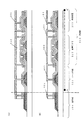
本発明の実施例を図1〜図3、図7に基づいて説明する。本実施例では液晶表示装置の作製方法を示し、基板上に画素部のTFTを逆スタガ型で作製し、前記TFTに接続する保持容量を作製する方法について工程に従って詳細に説明する。また、図1〜図3には、前記基板の端部に設けられた他の基板に設けた回路の配線と電気的に接続するための端子部を作製工程に同時に示した。尚、図1〜図3の断面図は図7のA〜A’の断面である。 An embodiment of the present invention will be described with reference to FIGS. In this embodiment, a manufacturing method of a liquid crystal display device is shown, and a method of manufacturing a TFT of a pixel portion with a reverse stagger type on a substrate and manufacturing a storage capacitor connected to the TFT will be described in detail according to steps. FIGS. 1 to 3 also show a terminal portion for electrical connection with circuit wiring provided on another substrate provided at an end portion of the substrate in the manufacturing process. The cross-sectional views of FIGS. 1 to 3 are cross-sections A to A ′ of FIG. 7.
最初に、透光性有する基板100を用いて半導体表示装置を作成する。用いることのできる基板として、コーニング社の#7059ガラスや#1737ガラスなどに代表されるバリウムホウケイ酸ガラスやアルミノホウケイ酸ガラスなどのガラス基板を用いることができる。更に他の基板として、石英基板、プラスチック基板などの透光性基板を用いることもできる。
First, a semiconductor display device is formed using a light-transmitting
上記基板100上に導電層を基板全面に形成した後、第1のフォトリソグラフィー工程を行い、レジストマスクを形成し、エッチングにより不要な部分を除去して配線及び電極(ソース配線102、ゲート電極103,104、保持容量105、及び端子101)を形成する。(図1(A))
After a conductive layer is formed over the entire surface of the
上記の配線及び電極の材料としては、Ti、Ta、W、Mo、Cr、Ndから選ばれた元素、前記元素を成分とする合金、または前記元素を成分とする窒化物で形成する。さらに、Ti、Ta、W、Mo、Cr、Ndから選ばれた元素、前記元素を成分とする合金、または前記元素を成分とする窒化物から複数選択し、それを積層することもできる。 The wiring and electrode materials are made of an element selected from Ti, Ta, W, Mo, Cr, and Nd, an alloy containing the element as a component, or a nitride containing the element as a component. Further, a plurality of elements selected from Ti, Ta, W, Mo, Cr, and Nd, an alloy containing the element as a component, or a nitride containing the element as a component can be selected and stacked.
次に、ソース配線102及び端子部101にCu被膜106及び110をメッキ法により形成する。(図1(B))従来の5インチ程度の画面サイズであるならば、Ti、Ta、W、Mo、Cr、Ndから選ばれた元素、前記元素を成分とする合金、または前記元素を成分とする窒化物で形成しても配線抵抗は問題にならなかったが、画面サイズが大画面化するとそれぞれの配線の長さが増加して、配線抵抗が高くなる問題が発生し、消費電力の増大を引き起こす。よって、Cu被膜106をソース配線のみにメッキすることで配線抵抗を下げることが可能となり、低消費電力を実現することができる。本実施例では金属被膜にCuを使用したが、他にも、Ag、Au、Cr、Fe、Ni、Ptまたはこれらの合金を用いることもできる。
Next,
また、上記各作製方法において、前記メッキを施す工程において、前記画素部のソース配線は、同電位となるように配線でつなげられていることを特徴としている。また、前記同電位となるようにつなげられた配線は、メッキ処理後にレーザー光(CO2レーザー等)で分断してもよいし、メッキ処理後に前記基板と同時に分断してもよい。また、これらの配線パターンでショートリングを形成しても良い。 In each of the above manufacturing methods, in the step of performing plating, the source wiring of the pixel portion is connected by wiring so as to have the same potential. Further, the wiring connected to have the same potential may be divided by a laser beam (CO 2 laser or the like) after the plating process, or may be divided simultaneously with the substrate after the plating process. Moreover, you may form a short ring with these wiring patterns.
次に、絶縁膜107を全面に成膜する。絶縁膜は窒化シリコン膜を用い、膜厚を50〜200nmとし、好ましくは150nmの厚さで形成する。尚、ゲート絶縁膜は窒化シリコン膜に限定されるものではなく酸化シリコン膜、酸化窒化シリコン膜、酸化タンタル膜などの絶縁膜を用いることもできる。(図1(C))
Next, an insulating
次に、絶縁膜107上に、50〜200nm好ましくは100〜150nmの膜厚で第1の非晶質半導体膜108を、プラズマCVD法やスパッタ法などの公知の方法で全面に成膜する。代表的には非晶質シリコン(a−Si)膜を100nmの膜厚で成膜する。(図1(C))
Next, a first
次に、一導電型(n型またはp型)の不純物元素を含有する第2の非晶質半導体膜109を20〜80nmの厚さで成膜する。一導電型(n型またはp型)を付与する不純物元素を含む第2の非晶質半導体膜109は、プラズマCVD法やスパッタ法などの公知の方法で全面に成膜する。本実施例ではリンが添加されたシリコンターゲットを用いてn型の不純物元素を含有する第2の非晶質半導体膜109を成膜した。(図1(C))
Next, a second
次に、第2のフォトリソグラフィー工程によりレジストマスク205,206を形成し、エッチングにより不要な部分を除去してソース配線311を形成する。この際のエッチング方法としてウエットエッチングまたはドライエッチングを用いる。(図2(A))
Next, resist
このエッチング工程で、レジストマスク205,206以外の場所は第2の非晶質半導体膜109、及び第1の非晶質半導体膜108を順次エッチングしていき、画素部のTFT312は第2の非晶質半導体膜203、及び第1の非晶質半導体膜201が形成される。また保持容量313は第2の非晶質半導体膜204、及び第1の非晶質半導体膜202が形成される。
In this etching process, the second
次に、レジストマスク205,206を除去した後、第3のフォトリソグラフィー工程を行い、レジストマスク207を形成して、エッチングにより不要な部分を除去して第1の非晶質半導体膜208、第2の非晶質半導体膜209,210,211を形成する。(図2(B))
Next, after removing the resist
次に、上記レジストマスク207を除去した後、プラズマCVD法により150nm厚の酸化窒化シリコン膜から成る第1の層間絶縁膜213をソース配線311、画素部のTFT312、及び保持容量313を覆うように成膜する。(図2(C))
Next, after removing the resist
次に、酸化窒化シリコン膜から成る第1の層間絶縁膜213上に、1.6μm厚のアクリル樹脂から成る有機絶縁材料である第2の層間絶縁膜302を成膜する。本実施例では第2の層間絶縁膜にアクリル樹脂から成る有機絶縁材料を選択したが、有機材料としてはポリイミド等でも良く、更に無機材料を選択しても良い。その後、第4のフォトリソグラフィー工程を行い、レジストマスク301を形成して、その後ドライエッチング工程により、ソース配線311と第2の非晶質半導体膜209を電気的に接続するためのコンタクトホールを形成する。また、同時に保持容量313と第2の非晶質半導体膜211を電気的に接続するためのコンタクトホールを形成する。また、ゲート配線と端子部310を電気的に接続するためのコンタクトホールを端子部分に形成する。(図3(A))
Next, a second
次に、ITO(Indium−Ti−Oxide)等の透明電極膜を110nmの厚さで成膜する。その後、第5のフォトリソグラフィー工程とエッチング工程を行うことにより、透明画素電極309を形成する。(図3(B))
Next, a transparent electrode film such as ITO (Indium-Ti-Oxide) is formed to a thickness of 110 nm. Thereafter, a
次に、金属配線を形成するために、第6のフォトリソグラフィー工程とエッチング工程を行う。ソース配線311と第2の非晶質半導体膜209を電気的に接続するために金属配線303を形成する。また、第2の非晶質半導体膜211と透明画素電極309を電気的に接続する金属配線305を形成する。また、透明画素電極309と保持容量313を電気的に接続する金属配線306を形成する。また、ゲート電極と端子部310を電気的に接続するための金属配線308を形成する。尚、金属配線材料としては、50nm厚のTi膜と500nm厚のAl−Ti合金膜の積層膜を使用することができる。(図3(C))
Next, in order to form a metal wiring, a sixth photolithography process and an etching process are performed. A metal wiring 303 is formed in order to electrically connect the source wiring 311 and the second
実施例1に示した半導体表示装置の作製方法は、ITO等の透明画素電極を形成した後に金属配線を形成したが、金属配線を形成した後にITO等の透明画素電極を形成した半導体表示装置の作製全体のフォトリソグラフィー工程数も同一である。よって、金属配線とITO等の透明画素電極はどちらを先に形成しても良い。 In the manufacturing method of the semiconductor display device shown in the first embodiment, the metal wiring is formed after forming the transparent pixel electrode such as ITO. However, the semiconductor display device in which the transparent pixel electrode such as ITO is formed after forming the metal wiring. The number of photolithography steps in the entire production is the same. Therefore, either the metal wiring or the transparent pixel electrode such as ITO may be formed first.
以上のような6回のフォトリソグラフィー工程により、Cuメッキを施したソース配線311と、逆スタガ型の画素部のTFT312及び保持容量313と、端子部310で構成された透過型の半導体表示装置を作製することができる。 Through a photolithography process of six times as described above, a transmissive semiconductor display device including the source wiring 311 plated with Cu, the TFT 312 and the storage capacitor 313 of the inverted staggered pixel portion, and the terminal portion 310 is manufactured. Can be produced.
尚、本実施例により得られる非晶質半導体膜で活性層を形成したTFTは、電界効果移動度が小さく1cm2/Vsec程度しか得られていない。そのために、画像表示を行うための駆動回路はICチップで形成され、TAB(Tape Automated Bonding)方式やCOG(Chip on glass)方式で実装されている。 Note that a TFT in which an active layer is formed of an amorphous semiconductor film obtained according to this embodiment has a small field effect mobility and can be obtained only about 1 cm 2 / Vsec. For this purpose, a driving circuit for displaying an image is formed by an IC chip and mounted by a TAB (Tape Automated Bonding) method or a COG (Chip on glass) method.
実施例1では反射型の半導体表示装置を6回のフォトリソグラフィー工程で作製することができることを示したが、本実施例では5回のフォトリソグラフィー工程で反射型の半導体表示装置を作製する方法を図4に示す。
In
本実施例は実施例1の図3(A)の状態まで同一の工程であるので、異なる工程についてのみ以下に示す。尚、図3(A)に対応する箇所は同一の符号を用いた。 Since this example is the same process up to the state of FIG. 3A of Example 1, only different processes will be described below. In addition, the same code | symbol was used for the location corresponding to FIG. 3 (A).
まず、実施例1に従って図3(A)の状態を得た後、第5のフォトリソグラフィー工程とエッチング工程を行うことにより、ソース配線311と第2の非晶質半導体膜209を電気的に接続するために金属配線402を形成する。また、同時に画素電極401を形成する。さらに、端子部と電気的に接続する金属配線405を同時に形成する。(図4(B))
First, after obtaining the state of FIG. 3A in accordance with
このように合計5回のフォトリソグラフィー工程により、金属被膜メッキを施したソース配線311と、逆スタガ型の画素部のTFT312、保持容量313と、及び端子部310で構成された反射型の半導体表示装置を作製することができる。 In this way, a reflective semiconductor display composed of the source wiring 311 plated with the metal film, the TFT 312 of the inverted staggered pixel portion, the storage capacitor 313, and the terminal portion 310 by a total of five photolithography processes. A device can be made.
実施例1及び実施例2では、メッキ工程を第1のフォトリソグラフィー工程の後に行ったが、本実施例では第4のフォトリソグラフィー工程の後にメッキ工程を行うことを図9〜図11に基づいて説明する。 In Example 1 and Example 2, the plating process was performed after the first photolithography process, but in this example, the plating process is performed after the fourth photolithography process, based on FIGS. 9 to 11. explain.
最初に、透光性有する基板900を用いて半導体表示装置を作成する。用いることのできる基板として、コーニング社の#7059ガラスや#1737ガラスなどに代表されるバリウムホウケイ酸ガラスやアルミノホウケイ酸ガラスなどのガラス基板を用いることができる。更に他の基板として、石英基板、プラスチック基板などの透光性基板を用いることもできる。
First, a semiconductor display device is formed using a light-transmitting
上記基板上に導電層を基板全面に形成した後、第1のフォトリソグラフィー工程を行い、レジストマスクを形成し、エッチングにより不要な部分を除去して配線及び電極(ソース配線902、ゲート電極903,904、保持容量905、及び端子901)を形成する。(図9(A))
After a conductive layer is formed over the entire surface of the substrate, a first photolithography process is performed, a resist mask is formed, unnecessary portions are removed by etching, and wirings and electrodes (
上記の配線及び電極の材料としては、Ti、Ta、W、Mo、Cr、Ndから選ばれた元素、前記元素を成分とする合金、または前記元素を成分とする窒化物で形成する。さらに、Ti、Ta、W、Mo、Cr、Ndから選ばれた元素、前記元素を成分とする合金、または前記元素を成分とする窒化物から複数選択し、それを積層することもできる。 The wiring and electrode materials are made of an element selected from Ti, Ta, W, Mo, Cr, and Nd, an alloy containing the element as a component, or a nitride containing the element as a component. Further, a plurality of elements selected from Ti, Ta, W, Mo, Cr, and Nd, an alloy containing the element as a component, or a nitride containing the element as a component can be selected and stacked.
次に、絶縁膜906を全面に成膜する。絶縁膜は窒化シリコン膜を用い、膜厚を50〜200nmとし、好ましくは150nmの厚さで形成する。尚、ゲート絶縁膜は窒化シリコン膜に限定されるものではなく酸化シリコン膜、酸化窒化シリコン膜、酸化タンタル膜などの絶縁膜を用いることもできる。(図9(B))
Next, an insulating
次に、絶縁膜906上に、50〜200nm好ましくは100〜150nmの膜厚で第1の非晶質半導体膜907を、プラズマCVD法やスパッタ法などの公知の方法で全面に成膜する。代表的には非晶質シリコン(a−Si)膜を100nmの膜厚で成膜する。(図9(B))
Next, a first
次に、一導電型(n型またはp型)の不純物元素を含有する第2の非晶質半導体膜908を20〜80nmの厚さで成膜する。一導電型(n型またはp型)を付与する不純物元素を含む第2の非晶質半導体膜908は、プラズマCVD法やスパッタ法などの公知の方法で全面に成膜する。本実施例ではリンが添加されたシリコンターゲットを用いてn型の不純物元素を含有する第2の非晶質半導体膜908を成膜した。(図9(B))
Next, a second
次に、第2のフォトリソグラフィー工程によりレジストマスク909,910を形成し、エッチングにより不要な部分を除去してソース配線1111を形成する。この際のエッチング方法としてウエットエッチングまたはドライエッチングを用いる。(図9(C))
Next, resist
このエッチング工程で、レジストマスク909,910以外の場所は第2の非晶質半導体膜908、及び第1の非晶質半導体膜907を順次エッチングしていき、画素部のTFT1112は第2の非晶質半導体膜913、及び第1の非晶質半導体膜911が形成される。また保持容量1113は第2の非晶質半導体膜914、及び第1の非晶質半導体膜912が形成される。
In this etching process, the second
次に、レジストマスク909,910を除去した後、第3のフォトリソグラフィー工程を行い、レジストマスク1001を形成して、エッチングにより不要な部分を除去して第1の非晶質半導体膜1002、第2の非晶質半導体膜1003,1004,1005を形成する。(図10(A))
Next, after removing the resist
次に、上記レジストマスク1001を除去した後、プラズマCVD法により150nm厚の酸化窒化シリコン膜から成る第1の層間絶縁膜1006をソース配線1111、画素部のTFT1112、及び保持容量1113を覆うように成膜する。(図10(B))
Next, after removing the resist mask 1001, a first interlayer insulating film 1006 made of a silicon oxynitride film having a thickness of 150 nm is covered by a plasma CVD method so as to cover the source wiring 1111, the
次に、酸化窒化シリコン膜から成る第1の層間絶縁膜1006上に、1.6μm厚のアクリル樹脂から成る有機絶縁材料である第2の層間絶縁膜1008を成膜する。本実施例では第2の層間絶縁膜にアクリル樹脂から成る有機絶縁材料を選択したが、有機材料としてはポリイミド等でも良く、更に無機材料を選択しても良い。その後、第4のフォトリソグラフィー工程を行い、レジストマスク1007を形成して、その後ドライエッチング工程により、ソース配線1111上と端子部1110上の第1の層間絶縁膜と第2の層間絶縁膜を取り除く。また、保持容量1113と第2の非晶質半導体膜1005を電気的に接続するためのコンタクトホールを形成する。(図10(C))
Next, a second interlayer insulating film 1008 that is an organic insulating material made of an acrylic resin having a thickness of 1.6 μm is formed on the first interlayer insulating film 1006 made of a silicon oxynitride film. In this embodiment, an organic insulating material made of an acrylic resin is selected for the second interlayer insulating film, but polyimide or the like may be used as the organic material, and an inorganic material may be further selected. Thereafter, a fourth photolithography process is performed to form a resist mask 1007, and then the first interlayer insulating film and the second interlayer insulating film on the source wiring 1111 and the terminal portion 1110 are removed by a dry etching process. . In addition, a contact hole for electrically connecting the storage capacitor 1113 and the second
次に、ソース配線1110及び端子部1111にCu被膜1101及び1102をメッキ法により形成する。(図11(A))ここで用いる金属被膜は実施例1と同様にAg、Au、Cr、Fe、Ni、Ptまたはこれらの合金を用いることもできる。 Next, Cu coatings 1101 and 1102 are formed on the source wiring 1110 and the terminal portion 1111 by a plating method. (FIG. 11 (A)) The metal coating used here may be Ag, Au, Cr, Fe, Ni, Pt or an alloy thereof as in the first embodiment.
また、実施例1と同様に上記各作製方法において、前記メッキを施す工程において、前記画素部のソース配線は、同電位となるように配線でつなげられていることを特徴としている。また、前記同電位となるようにつなげられた配線は、メッキ処理後にレーザー光(CO2レーザー等)で分断してもよいし、メッキ処理後に前記基板と同時に分断してもよい。また、これらの配線パターンでショートリングを形成しても良い。
Further, as in
次に、ITO(Indium−Ti−Oxide)等の透明電極膜を110nmの厚さで成膜する。その後、第5のフォトリソグラフィー工程とエッチング工程を行うことにより、透明画素電極1103を形成する。(図11(B)) Next, a transparent electrode film such as ITO (Indium-Ti-Oxide) is formed to a thickness of 110 nm. Thereafter, a transparent pixel electrode 1103 is formed by performing a fifth photolithography process and an etching process. (Fig. 11 (B))
次に、金属配線を形成するために、第6のフォトリソグラフィー工程とエッチング工程を行う。ソース配線1111と第2の非晶質半導体膜1003を電気的に接続するために金属配線1105を形成する。また、第2の非晶質半導体膜1005と透明画素電極1103を電気的に接続する金属配線1107を形成する。また、透明画素電極1103と保持容量1113を電気的に接続する金属配線1108を形成する。また、ゲート電極と端子部1110を電気的に接続するための金属配線1104を形成する。尚、金属配線材料としては、50nm厚のTi膜と500nm厚のAl−Ti合金膜の積層膜を使用することができる。(図11(C))
Next, in order to form a metal wiring, a sixth photolithography process and an etching process are performed. In order to electrically connect the source wiring 1111 and the second amorphous semiconductor film 1003, a metal wiring 1105 is formed. In addition, a metal wiring 1107 that electrically connects the second
実施例3に示した半導体表示装置の作製方法は、ITO等の透明画素電極を形成した後に金属配線を形成したが、金属配線を形成した後にITO等の透明画素電極を形成した半導体表示装置の作製全体のフォトリソグラフィー工程数も同一である。よって、金属配線とITO等の透明画素電極はどちらを先に形成しても良い。 In the method of manufacturing the semiconductor display device shown in Example 3, the metal wiring is formed after forming the transparent pixel electrode such as ITO. However, the semiconductor display device in which the transparent pixel electrode such as ITO is formed after forming the metal wiring. The number of photolithography steps in the entire production is the same. Therefore, either the metal wiring or the transparent pixel electrode such as ITO may be formed first.
以上のような6回のフォトリソグラフィー工程により、Cuメッキを施したソース配線1111と、逆スタガ型の画素部のTFT1112及び保持容量1113と、端子部1110で構成された透過型の半導体表示装置を作製することができる。
Through the six photolithography processes as described above, a transmissive semiconductor display device including the source wiring 1111 subjected to Cu plating, the
また、画素電極に金属配線と同じ金属を用いれば5回のフォトリソグラフィー工程で反射型の半導体装置を作製することができる。 In addition, when the same metal as the metal wiring is used for the pixel electrode, a reflective semiconductor device can be manufactured through five photolithography processes.
尚、本実施例も実施例1と同様に画像表示を行うためにICチップで形成された駆動回路を実装している。 In this embodiment, a drive circuit formed of an IC chip is mounted in order to display an image as in the first embodiment.
実施例1〜実施例3までは、画素部のTFTがチャネルエッチ型の半導体装置であったが、本実施例では、画素部のTFTがチャネルストップ型の半導体装置の実施例を図12〜図14に基づいて説明する。 In the first to third embodiments, the TFT in the pixel portion is a channel etch type semiconductor device, but in this embodiment, an embodiment in which the TFT in the pixel portion is a channel stop type semiconductor device is shown in FIGS. 14 will be described.
最初に、透光性有する基板1200を用いて半導体表示装置を作成する。用いることのできる基板として、コーニング社の#7059ガラスや#1737ガラスなどに代表されるバリウムホウケイ酸ガラスやアルミノホウケイ酸ガラスなどのガラス基板を用いることができる。更に他の基板として、石英基板、プラスチック基板などの透光性基板を用いることもできる。
First, a semiconductor display device is manufactured using a light-transmitting
上記基板上に導電層を基板全面に形成した後、第1のフォトリソグラフィー工程を行い、レジストマスクを形成し、エッチングにより不要な部分を除去して配線及び電極(ソース配線1202、ゲート電極1203,1204、保持容量1205、及び端子1201)を形成する。(図12(A))
After a conductive layer is formed over the entire surface of the substrate, a first photolithography process is performed, a resist mask is formed, unnecessary portions are removed by etching, and wirings and electrodes (source wiring 1202,
上記の配線及び電極の材料としては、Ti、Ta、W、Mo、Cr、Ndから選ばれた元素、前記元素を成分とする合金、または前記元素を成分とする窒化物で形成する。さらに、Ti、Ta、W、Mo、Cr、Ndから選ばれた元素、前記元素を成分とする合金、または前記元素を成分とする窒化物から複数選択し、それを積層することもできる。 The wiring and electrode materials are made of an element selected from Ti, Ta, W, Mo, Cr, and Nd, an alloy containing the element as a component, or a nitride containing the element as a component. Further, a plurality of elements selected from Ti, Ta, W, Mo, Cr, and Nd, an alloy containing the element as a component, or a nitride containing the element as a component can be selected and stacked.
次に、ソース配線1202及び端子部1201にCu被膜1206及び1209をメッキ法により形成する。(図12(B))従来の5インチ程度の画面サイズであるならば、Ti、Ta、W、Mo、Cr、Ndから選ばれた元素、前記元素を成分とする合金、または前記元素を成分とする窒化物で形成しても配線抵抗は問題にならなかったが、画面サイズが大画面化するとそれぞれの配線の長さが増加して、配線抵抗が高くなる問題が発生し、消費電力の増大を引き起こす。よって、Cu膜1206をソース配線のみにメッキすることで配線抵抗を下げることが可能となり、低消費電力を実現することができる。本実施例では金属被膜にCuを使用したが、他にも、Ag、Au、Cr、Fe、Ni、Ptまたはこれらの合金を用いることもできる。
Next,
また、実施例1と同様に上記各作製方法において、前記メッキを施す工程において、前記画素部のソース配線は、同電位となるように配線でつなげられていることを特徴としている。また、前記同電位となるようにつなげられた配線は、メッキ処理後にレーザー光(CO2レーザー等)で分断してもよいし、メッキ処理後に前記基板と同時に分断してもよい。また、これらの配線パターンでショートリングを形成しても良い。
Further, as in
次に、絶縁膜1207を全面に成膜する。絶縁膜は窒化シリコン膜を用い、膜厚を50〜200nmとし、好ましくは150nmの厚さで形成する。尚、ゲート絶縁膜は窒化シリコン膜に限定されるものではなく酸化シリコン膜、酸化窒化シリコン膜、酸化タンタル膜などの絶縁膜を用いることもできる。(図12(C))
Next, an insulating
次に、絶縁膜1207上に、50〜200nm好ましくは100〜150nmの膜厚で非晶質半導体膜1208を、プラズマCVD法やスパッタ法などの公知の方法で全面に成膜する。代表的には非晶質シリコン(a−Si)膜を100nmの膜厚で成膜する。(図12(C))
Next, an amorphous semiconductor film 1208 is formed over the entire surface of the insulating
次に、第2のフォトリソグラフィー工程によりレジストマスク1301,1302を形成し、エッチングにより不要な部分を除去してソース配線1411を形成する。この際のエッチング方法としてウエットエッチングまたはドライエッチングを用いる。(図13(A)) Next, resist masks 1301 and 1302 are formed by a second photolithography process, unnecessary portions are removed by etching, and a source wiring 1411 is formed. As an etching method at this time, wet etching or dry etching is used. (FIG. 13 (A))
このエッチング工程で、レジストマスク1301,1302以外の場所は非晶質半導体膜1208をエッチングしていき、画素部のTFT1412は非晶質半導体膜1304が形成される。また保持容量1413は非晶質半導体膜1304が形成される。(図13(A))
In this etching process, the amorphous semiconductor film 1208 is etched in places other than the resist masks 1301 and 1302, and the
次に、非晶質半導体層1303上に酸化シリコンまたは窒化シリコンから成る絶縁膜を100〜200nmの厚さに形成する。図13(A)は、ゲート電極をマスクとする裏面からの露光プロセスにより、自己整合的にチャネル保護膜とする第2の絶縁層1305,1306を半導体層1303上に形成する。 Next, an insulating film made of silicon oxide or silicon nitride is formed to a thickness of 100 to 200 nm over the amorphous semiconductor layer 1303. In FIG. 13A, second insulating layers 1305 and 1306 serving as channel protective films are formed on the semiconductor layer 1303 in a self-aligning manner by an exposure process from the back surface using the gate electrode as a mask.
次に、nチャネル型TFTのLDD(Lightly Doped Drain)領域を形成するためのドーピング工程を行う。ドーピングの方法はイオンドープ方法もしくはイオン注入法で行う。n型の不純物としてリンを添加し、第2の絶縁層1305,1306をマスクとして形成される不純物領域1307〜1309を形成する。この領域のドナー濃度は1×10¹⁶〜1×10¹⁷/cm3の濃度とする。(図13(B)) Next, a doping process for forming an LDD (Lightly Doped Drain) region of the n-channel TFT is performed. Doping is performed by ion doping or ion implantation. Phosphorus is added as an n-type impurity to form impurity regions 1307 to 1309 formed using the second insulating layers 1305 and 1306 as masks. The donor concentration in this region is 1 × 10 16 to 1 × 10 17 / cm 3 . (Fig. 13B)
次に、プラズマCVD法により150nm厚の酸化窒化シリコン膜から成る第1の層間絶縁膜1311をソース配線1411、画素部のTFT1412、及び保持容量1413を覆うように成膜する。(図13(C)) Next, a first interlayer insulating film 1311 made of a silicon oxynitride film with a thickness of 150 nm is formed by plasma CVD so as to cover the source wiring 1411, the TFT 1412 in the pixel portion, and the storage capacitor 1413. (Fig. 13 (C))
次に、酸化窒化シリコン膜から成る第1の層間絶縁膜1311上に、1.6μm厚のアクリル樹脂から成る有機絶縁材料である第2の層間絶縁膜1402を成膜する。本実施例では第2の層間絶縁膜にアクリル樹脂から成る有機絶縁材料を選択したが、有機材料としてはポリイミド等でも良く、更に無機材料を選択しても良い。その後、第4のフォトリソグラフィー工程を行い、レジストマスク1401を形成して、その後ドライエッチング工程により、ソース配線1411と非晶質半導体膜1307を電気的に接続するためのコンタクトホールを形成する。
また、同時に保持容量1413と非晶質半導体膜1309を電気的に接続するためのコンタクトホールを形成する。また、ゲート配線と端子部1410を電気的に接続するためのコンタクトホールを端子部分に形成する。(図14(A))
Next, a second
At the same time, a contact hole for electrically connecting the storage capacitor 1413 and the
次に、ITO(Indium−Ti−Oxide)等の透明電極膜を110nmの厚さで成膜する。その後、第5のフォトリソグラフィー工程とエッチング工程を行うことにより、透明画素電極1403を形成する。(図14(B)) Next, a transparent electrode film such as ITO (Indium-Ti-Oxide) is formed to a thickness of 110 nm. Thereafter, a transparent pixel electrode 1403 is formed by performing a fifth photolithography process and an etching process. (Fig. 14B)
次に、金属配線を形成するために、第6のフォトリソグラフィー工程とエッチング工程を行う。ソース配線1411と非晶質半導体膜1307を電気的に接続するために金属配線1405を形成する。また、非晶質半導体膜1309と透明画素電極1403を電気的に接続する金属配線1407を形成する。また、透明画素電極1403と保持容量1413を電気的に接続する金属配線1408を形成する。また、ゲート電極と端子部1410を電気的に接続するための金属配線1404を形成する。尚、金属配線材料としては、50nm厚のTi膜と500nm厚のAl−Ti合金膜の積層膜を使用することができる。(図14(C))
Next, in order to form a metal wiring, a sixth photolithography process and an etching process are performed. A
実施例4に示した半導体表示装置の作製方法は、ITO等の透明画素電極を形成した後に金属配線を形成したが、金属配線を形成した後にITO等の透明画素電極を形成した半導体表示装置の作製全体のフォトリソグラフィー工程数も同一である。よって、金属配線とITO等の透明画素電極はどちらを先に形成しても良い。 In the method of manufacturing the semiconductor display device shown in Example 4, the metal wiring is formed after forming the transparent pixel electrode such as ITO, but the semiconductor display device in which the transparent pixel electrode such as ITO is formed after forming the metal wiring. The number of photolithography steps in the entire production is the same. Therefore, either the metal wiring or the transparent pixel electrode such as ITO may be formed first.
以上のような6回のフォトリソグラフィー工程により、Cuメッキを施したソース配線1411と、逆スタガ型の画素部のTFT1412及び保持容量1413と、端子部1410で構成された透過型の半導体表示装置を作製することができる。 Through a photolithography process of six times as described above, a transmissive semiconductor display device including a source wiring 1411 subjected to Cu plating, a TFT 1412 and a storage capacitor 1413 of an inverted staggered pixel portion, and a terminal portion 1410 is manufactured. Can be produced.
また、画素電極を金属配線と同じ金属を用いれば5回のフォトリソグラフィー工程で反射型の半導体装置を作製することができる。 In addition, if the same metal as the metal wiring is used for the pixel electrode, a reflective semiconductor device can be manufactured through five photolithography processes.
尚、本実施例も実施例1と同様に画像表示を行うためにICチップで形成された駆動回路を実装している。 In this embodiment, a drive circuit formed of an IC chip is mounted in order to display an image as in the first embodiment.
本発明を実施して作製されたアクティブマトリクス基板および液晶表示装置は様々な電気光学装置に用いることができる。即ち、それら電気光学装置を表示部として組み込んだ電子機器全てに本発明を実施できる。 The active matrix substrate and the liquid crystal display device manufactured by implementing the present invention can be used for various electro-optical devices. That is, the present invention can be implemented in all electronic devices in which these electro-optical devices are incorporated as display units.
上記の様な電子機器としては、ビデオカメラ、デジタルカメラ、プロジェクター(リア型またはフロント型)、ヘッドマウントディスプレイ(ゴーグル型ディスプレイ)、カーナビゲーション、パーソナルコンピュータ、携帯情報端末(モバイルコンピュータ、携帯電話または電子書籍等)などが挙げられる。それらの一例を図5および図6に示す。 The above electronic devices include a video camera, a digital camera, a projector (rear type or front type), a head mounted display (goggles type display), a car navigation system, a personal computer, a personal digital assistant (mobile computer, mobile phone or electronic). Books). Examples of these are shown in FIGS.
図5(A)はパーソナルコンピュータであり、本体501、画像入力部502、表示部503、キーボード504等を含む。本発明を表示部503に適用することができる。 FIG. 5A illustrates a personal computer, which includes a main body 501, an image input portion 502, a display portion 503, a keyboard 504, and the like. The present invention can be applied to the display portion 503.
図5(B)はモバイルコンピュータであり、本体505、表示部506、カメラ部507、受像部508、操作スイッチ509等を含む。本発明は表示部に適用できる。 FIG. 5B illustrates a mobile computer, which includes a main body 505, a display portion 506, a camera portion 507, an image receiving portion 508, an operation switch 509, and the like. The present invention can be applied to a display unit.
図5(C)はプログラムを記録した記録媒体(以下、記録媒体と呼ぶ)を用いるプレーヤーであり、本体510、表示部511、スピーカー部512、記録媒体513、操作スイッチ514等を含む。なお、このプレーヤーは記録媒体としてDVD(Digtial Versatile Disc)、CD等を用い音楽鑑賞や映画鑑賞やゲームやインターネットを行うことができる。本発明は表示部511に適用することができる。 FIG. 5C shows a player using a recording medium (hereinafter referred to as a recording medium) in which a program is recorded, and includes a main body 510, a display portion 511, a speaker portion 512, a recording medium 513, an operation switch 514, and the like. This player can use a DVD (Digital Versatile Disc), a CD, or the like as a recording medium to enjoy music, movies, games, and the Internet. The present invention can be applied to the display portion 511.
図6(A)は携帯書籍(電子書籍)であり、本体601、表示部602,603、記憶媒体604、操作スイッチ605、アンテナ606等を含む。本発明は表示部602,603に適用することができる。
FIG. 6A illustrates a portable book (electronic book), which includes a main body 601, display portions 602 and 603, a
図6(B)はディスプレイであり、本体607、表示部608、支持台609等を含む。本発明は表示部608に適用することができる。
FIG. 6B shows a display, which includes a main body 607, a display portion 608, a
以上の様に、本発明の適用範囲は極めて広く、あらゆる分野の電子機器に適用することが可能である。また、本実施例の電子機器は実施形態1、実施形態2、実施例1〜実施例5のどのような組み合わせからなる構成を用いても実現することができる。
As described above, the application range of the present invention is extremely wide and can be applied to electronic devices in various fields. In addition, the electronic device of this example can be realized by using any combination of
Claims (6)
前記ゲート電極上に形成された絶縁膜と、
前記絶縁膜上に形成された第1の非晶質半導体膜と、
前記第1の非晶質半導体膜上に形成されたn型を付与する不純物元素を有する第2の非晶質半導体膜を有する薄膜トランジスタを画素部に用い、端子部を有する半導体装置であって、
前記第2の非晶質半導体膜にソース領域、ドレイン領域が形成され、
前記第2の非晶質半導体膜のソース領域、ドレイン領域のいずれか一方とソース配線が、前記絶縁膜上の第1の金属配線により電気的に接続され、
前記第2の非晶質半導体膜のソース領域、ドレイン領域のいずれか他方と画素電極が、前記絶縁膜上の第2の金属配線により電気的に接続され、
前記ゲート電極と前記端子部が第3の金属配線により電気的に接続され、
前記第1の金属配線と前記第2の金属配線と前記第3の金属配線は同一の金属から形成され、
前記ソース配線は前記絶縁膜下に形成され、
前記ソース配線と前記ゲート電極と前記端子部は同一平面上に形成され、同一の金属から形成され、
前記第3の金属配線はゲート配線であり、前記薄膜トランジスタ上に形成されていることを特徴とする半導体装置。 A gate electrode formed on an insulating surface;
An insulating film formed on the gate electrode;
A first amorphous semiconductor film formed on the insulating film;
A thin film transistor having a second amorphous semiconductor film having an impurity element imparting n-type formed on the first amorphous semiconductor film is used for a pixel portion, and a semiconductor device having a terminal portion,
A source region and a drain region are formed in the second amorphous semiconductor film,
Either the source region or the drain region of the second amorphous semiconductor film and the source wiring are electrically connected by the first metal wiring on the insulating film,
The other of the source region and the drain region of the second amorphous semiconductor film and the pixel electrode are electrically connected by a second metal wiring on the insulating film,
The gate electrode and the terminal portion are electrically connected by a third metal wiring,
The first metal wiring, the second metal wiring, and the third metal wiring are formed of the same metal,
The source wiring is formed under the insulating film,
The source wiring, the gate electrode, and the terminal portion are formed on the same plane and are formed of the same metal ,
The semiconductor device, wherein the third metal wiring is a gate wiring and is formed on the thin film transistor.
前記ゲート電極上に形成された絶縁膜と、
前記絶縁膜上に形成された第1の非晶質半導体膜と、
前記第1の非晶質半導体膜上に形成されたn型を付与する不純物元素を有する第2の非晶質半導体膜を有する薄膜トランジスタを画素部の薄膜トランジスタとし、端子部を有する半導体装置であって、
前記第2の非晶質半導体膜にソース領域、ドレイン領域が形成され、
前記第2の非晶質半導体膜のソース領域、ドレイン領域のいずれか一方とソース配線が、前記絶縁膜上の第1の金属配線により電気的に接続され、
前記第2の非晶質半導体膜のソース領域、ドレイン領域のいずれか他方と画素電極が、前記絶縁膜上の第2の金属配線により電気的に接続され、
前記ゲート電極と前記端子部が第3の金属配線により電気的に接続され、
前記第1の金属配線と前記第2の金属配線と前記第3の金属配線は同一の金属から形成され、
前記ソース配線は前記絶縁膜下に形成され、
前記ソース配線と前記ゲート電極と前記端子部は同一平面上に形成され、同一の金属から形成されており、
前記ソース配線と、前記画素電極は重なっており、
前記第3の金属配線はゲート配線であり、前記薄膜トランジスタ上に形成されていることを特徴とする半導体装置。 A gate electrode formed on an insulating surface;
An insulating film formed on the gate electrode;
A first amorphous semiconductor film formed on the insulating film;
A thin film transistor having a second amorphous semiconductor film containing an impurity element imparting n-type formed on the first amorphous semiconductor film is a thin film transistor of a pixel portion, and a semiconductor device having a terminal portion. ,
A source region and a drain region are formed in the second amorphous semiconductor film,
Either the source region or the drain region of the second amorphous semiconductor film and the source wiring are electrically connected by the first metal wiring on the insulating film,
The other of the source region and the drain region of the second amorphous semiconductor film and the pixel electrode are electrically connected by a second metal wiring on the insulating film,
The gate electrode and the terminal portion are electrically connected by a third metal wiring,
The first metal wiring, the second metal wiring, and the third metal wiring are formed of the same metal,
The source wiring is formed under the insulating film,
The source wiring, the gate electrode, and the terminal portion are formed on the same plane and are formed of the same metal,
The source wiring and the pixel electrode overlap ,
The semiconductor device, wherein the third metal wiring is a gate wiring and is formed on the thin film transistor.
前記画素電極は透明導電膜からなることを特徴とする半導体装置。 In claim 1 or claim 2,
The pixel device is made of a transparent conductive film.
前記ソース配線は表面に金属皮膜を有していることを特徴とする半導体装置。 In any one of Claims 1 thru | or 3,
The semiconductor device according to claim 1, wherein the source wiring has a metal film on a surface thereof.
前記第2の非晶質半導体膜上に第1の層間絶縁膜が形成されていることを特徴とする半導体装置。 In any one of Claims 1 thru | or 4,
A semiconductor device, wherein a first interlayer insulating film is formed on the second amorphous semiconductor film.
前記ソース配線と前記端子部は、前記第1乃至第3の金属配線と同一の金属から形成された金属配線で電気的に接続されていることを特徴とする半導体装置。 In any one of Claims 1 thru | or 5 ,
The semiconductor device, wherein the source wiring and the terminal portion are electrically connected by a metal wiring formed of the same metal as the first to third metal wirings.
Priority Applications (1)
| Application Number | Priority Date | Filing Date | Title |
|---|---|---|---|
| JP2007315900A JP4850168B2 (en) | 2007-12-06 | 2007-12-06 | Semiconductor device |
Applications Claiming Priority (1)
| Application Number | Priority Date | Filing Date | Title |
|---|---|---|---|
| JP2007315900A JP4850168B2 (en) | 2007-12-06 | 2007-12-06 | Semiconductor device |
Related Parent Applications (1)
| Application Number | Title | Priority Date | Filing Date |
|---|---|---|---|
| JP2000400280A Division JP4789322B2 (en) | 2000-12-11 | 2000-12-28 | Semiconductor device and manufacturing method thereof |
Related Child Applications (1)
| Application Number | Title | Priority Date | Filing Date |
|---|---|---|---|
| JP2011182531A Division JP5538331B2 (en) | 2011-08-24 | 2011-08-24 | Semiconductor device |
Publications (3)
| Publication Number | Publication Date |
|---|---|
| JP2008146068A JP2008146068A (en) | 2008-06-26 |
| JP2008146068A5 JP2008146068A5 (en) | 2008-08-14 |
| JP4850168B2 true JP4850168B2 (en) | 2012-01-11 |
Family
ID=39606241
Family Applications (1)
| Application Number | Title | Priority Date | Filing Date |
|---|---|---|---|
| JP2007315900A Expired - Fee Related JP4850168B2 (en) | 2007-12-06 | 2007-12-06 | Semiconductor device |
Country Status (1)
| Country | Link |
|---|---|
| JP (1) | JP4850168B2 (en) |
Families Citing this family (5)
| Publication number | Priority date | Publication date | Assignee | Title |
|---|---|---|---|---|
| JP2001257350A (en) | 2000-03-08 | 2001-09-21 | Semiconductor Energy Lab Co Ltd | Semiconductor device and its preparation method |
| TW525216B (en) | 2000-12-11 | 2003-03-21 | Semiconductor Energy Lab | Semiconductor device, and manufacturing method thereof |
| JP2010263182A (en) * | 2009-04-10 | 2010-11-18 | Toppan Printing Co Ltd | Thin film transistor, and image display unit |
| JP5538331B2 (en) * | 2011-08-24 | 2014-07-02 | 株式会社半導体エネルギー研究所 | Semiconductor device |
| JP5604477B2 (en) * | 2012-07-10 | 2014-10-08 | 株式会社半導体エネルギー研究所 | Display device |
Family Cites Families (6)
| Publication number | Priority date | Publication date | Assignee | Title |
|---|---|---|---|---|
| JPH05243333A (en) * | 1992-02-26 | 1993-09-21 | Nec Corp | Thin film field-effect transistor substrate |
| JP3387981B2 (en) * | 1992-10-09 | 2003-03-17 | 富士通株式会社 | Method of manufacturing thin film transistor matrix device |
| JPH07110495A (en) * | 1993-10-14 | 1995-04-25 | Hitachi Ltd | Active matrix liquid crystal device |
| JPH10319431A (en) * | 1997-05-15 | 1998-12-04 | Advanced Display:Kk | Thin film transistor array substrate |
| JP3868649B2 (en) * | 1999-01-22 | 2007-01-17 | 株式会社アドバンスト・ディスプレイ | Liquid crystal display device and manufacturing method thereof |
| JP4789322B2 (en) * | 2000-12-28 | 2011-10-12 | 株式会社半導体エネルギー研究所 | Semiconductor device and manufacturing method thereof |
-
2007
- 2007-12-06 JP JP2007315900A patent/JP4850168B2/en not_active Expired - Fee Related
Also Published As
| Publication number | Publication date |
|---|---|
| JP2008146068A (en) | 2008-06-26 |
Similar Documents
| Publication | Publication Date | Title |
|---|---|---|
| US9786687B2 (en) | Semiconductor device and manufacturing method thereof | |
| JP4118484B2 (en) | Method for manufacturing semiconductor device | |
| JP4118485B2 (en) | Method for manufacturing semiconductor device | |
| KR101448903B1 (en) | Semiconductor device and method for manufacturing semiconductor device | |
| JP2010217926A (en) | Liquid crystal display device | |
| JP4850168B2 (en) | Semiconductor device | |
| JP4789322B2 (en) | Semiconductor device and manufacturing method thereof | |
| JP6243953B2 (en) | Semiconductor device and electronic equipment | |
| JP6007269B2 (en) | Display device and electronic device | |
| JP5779690B2 (en) | Display device and electronic device | |
| JP5732500B2 (en) | Display device | |
| JP5538331B2 (en) | Semiconductor device | |
| JP2019050394A (en) | Semiconductor device and electronic apparatus | |
| JP2017142537A (en) | Semiconductor device and electronic apparatus | |
| JP4118704B2 (en) | Method for manufacturing liquid crystal display device | |
| JP2008083731A (en) | Semiconductor device | |
| JP4485481B2 (en) | Method for manufacturing semiconductor device | |
| JP4704363B2 (en) | Method for manufacturing semiconductor device |
Legal Events
| Date | Code | Title | Description |
|---|---|---|---|
| A521 | Written amendment |
Free format text: JAPANESE INTERMEDIATE CODE: A523 Effective date: 20080701 |
|
| A131 | Notification of reasons for refusal |
Free format text: JAPANESE INTERMEDIATE CODE: A131 Effective date: 20100706 |
|
| A521 | Written amendment |
Free format text: JAPANESE INTERMEDIATE CODE: A523 Effective date: 20100819 |
|
| A131 | Notification of reasons for refusal |
Free format text: JAPANESE INTERMEDIATE CODE: A131 Effective date: 20110105 |
|
| A521 | Written amendment |
Free format text: JAPANESE INTERMEDIATE CODE: A523 Effective date: 20110203 |
|
| A131 | Notification of reasons for refusal |
Free format text: JAPANESE INTERMEDIATE CODE: A131 Effective date: 20110719 |
|
| A521 | Written amendment |
Free format text: JAPANESE INTERMEDIATE CODE: A523 Effective date: 20110824 |
|
| TRDD | Decision of grant or rejection written | ||
| A01 | Written decision to grant a patent or to grant a registration (utility model) |
Free format text: JAPANESE INTERMEDIATE CODE: A01 Effective date: 20111011 |
|
| A01 | Written decision to grant a patent or to grant a registration (utility model) |
Free format text: JAPANESE INTERMEDIATE CODE: A01 |
|
| A61 | First payment of annual fees (during grant procedure) |
Free format text: JAPANESE INTERMEDIATE CODE: A61 Effective date: 20111018 |
|
| R150 | Certificate of patent or registration of utility model |
Free format text: JAPANESE INTERMEDIATE CODE: R150 |
|
| FPAY | Renewal fee payment (event date is renewal date of database) |
Free format text: PAYMENT UNTIL: 20141028 Year of fee payment: 3 |
|
| FPAY | Renewal fee payment (event date is renewal date of database) |
Free format text: PAYMENT UNTIL: 20141028 Year of fee payment: 3 |
|
| R250 | Receipt of annual fees |
Free format text: JAPANESE INTERMEDIATE CODE: R250 |
|
| R250 | Receipt of annual fees |
Free format text: JAPANESE INTERMEDIATE CODE: R250 |
|
| R250 | Receipt of annual fees |
Free format text: JAPANESE INTERMEDIATE CODE: R250 |
|
| LAPS | Cancellation because of no payment of annual fees |