JP4838517B2 - Illumination photographing apparatus and photographing apparatus - Google Patents
Illumination photographing apparatus and photographing apparatus Download PDFInfo
- Publication number
- JP4838517B2 JP4838517B2 JP2005039933A JP2005039933A JP4838517B2 JP 4838517 B2 JP4838517 B2 JP 4838517B2 JP 2005039933 A JP2005039933 A JP 2005039933A JP 2005039933 A JP2005039933 A JP 2005039933A JP 4838517 B2 JP4838517 B2 JP 4838517B2
- Authority
- JP
- Japan
- Prior art keywords
- value
- light
- luminance
- color evaluation
- illumination
- Prior art date
- Legal status (The legal status is an assumption and is not a legal conclusion. Google has not performed a legal analysis and makes no representation as to the accuracy of the status listed.)
- Expired - Fee Related
Links
Images


Landscapes
- Exposure Control For Cameras (AREA)
- Stroboscope Apparatuses (AREA)
Description
本発明は、閃光発光或いは連続発光を行って被写体を撮影するための照明撮影装置、照明装置及び撮影装置に関するものである。 The present invention relates to an illumination photographing apparatus, an illumination apparatus, and a photographing apparatus for photographing a subject by performing flash emission or continuous emission.
従来、写真撮影用の照明装置としては、キセノン管を発光させるストロボが一般的に用いられてきた。しかし、キセノン管とは色温度が異なる蛍光灯などの光源が被写界を照明している環境でストロボ撮影を行うと、得られる画像の色が画像中の場所によって異なって再現され、画像が不自然に見えてしまうという問題があった。この問題を解決する方法として、キセノン管によるストロボに代わる照明装置として、R(赤)、G(緑)、B(青)の発光ダイオード(以下「LED」という)を用いて、被写界を照明している光源と同じ色温度でLEDを発光させて被写界を照明する照明装置が提案されており(特許文献1参照)、R,G,BのLEDを用いた各種照明も利用されるようになってきた。 Conventionally, a strobe that emits light from a xenon tube has been generally used as an illumination device for taking a picture. However, if you take a stroboscopic shot in an environment where a light source such as a fluorescent light that has a different color temperature from the xenon tube illuminates the scene, the color of the resulting image will be reproduced differently depending on the location in the image. There was a problem that it looked unnatural. As a method for solving this problem, a lighting device in place of the flash according to the xenon tube, with R (red), G (green), B (blue) light emitting diode (hereinafter referred to as "LED"), a subject field There has been proposed an illumination device that illuminates an object scene by causing an LED to emit light at the same color temperature as the illuminating light source (see Patent Document 1), and various illuminations using R, G, and B LEDs are also used. It has come to be.
近年、高輝度のLEDが実用化されてきているとはいえ、写真撮影に用いる場合、画面全体を照明するのに十分な発光量をLEDにより得ることは困難である。主光源としては従来使われてきたものを用いるのが望ましい。 In recent years, although high-brightness LEDs have been put into practical use, when used for photography, it is difficult to obtain a sufficient amount of light emission to illuminate the entire screen. As the main light source, it is desirable to use a conventional light source.
(発明の目的)
本発明の目的は、主たる環境光とは異なる別の環境光が存在する状況での照明撮影時に、別の環境光が支配的な領域の色温度を主たる環境光が支配的な領域の色温度に一致させることを可能にする照明撮影装置及び撮影装置を提供することである。
(Object of invention)
The object of the present invention is to illuminate in the situation where there is another ambient light different from the main ambient light, and the color temperature of the area where the main ambient light is dominant. It is an object to provide an illumination photographing apparatus and a photographing apparatus that can be matched with temperature.
上記目的を達成するために、請求項1に記載の本発明は、第1の照明手段と、互いの発光量比を変更できる複数色の光源を有する第2の照明手段と、撮影画面内の複数の領域における被写体輝度を測定する輝度測定手段と、前記複数の領域の色評価値を求める評価手段と、前記第1の照明手段のみを発光させたときに前記輝度測定手段により測光を行って得られた輝度値である第1の輝度値と前記第1の照明手段及び前記第2の照明手段を発光させていないときに前記輝度測定手段により測光を行って得られた輝度値である第2の輝度値との差に基づく値が所定値以上である領域の色評価値に基づく第1の色評価値と、前記第1の輝度値と前記第2の輝度値との差に基づく値が所定値未満である領域の色評価値に基づく第2の色評価値との差を補償するような光量比で、前記第2の照明手段を発光させる制御手段と、を有する照明撮影装置とするものである。
In order to achieve the above object, the present invention described in
また同じく、請求項6に記載の本発明は、第1の照明手段と、互いの発光量比を変更できる複数色の光源を有する第2の照明手段を制御する撮影装置であって、撮影画面内の複数の領域における被写体輝度を測定する輝度測定手段と、前記複数の領域の色評価値を求める評価手段と、前記第1の照明手段のみを発光させたときに前記輝度測定手段により測光を行って得られた輝度値である第1の輝度値と前記第1の照明手段及び前記第2の照明手段を発光させていないときに前記輝度測定手段により測光を行って得られた輝度値である第2の輝度値との差に基づく値が所定値以上である領域の色評価値に基づく第1の色評価値と、前記第1の輝度値と前記第2の輝度値との差に基づく値が所定値未満である領域の色評価値に基づく第2の色評価値との差を補償するような光量比を求め、前記第2の照明手段が当該光量比で発光するように制御する制御手段と、を有する撮影装置とするものである。 Similarly, the present invention according to claim 6 is an imaging apparatus for controlling the first illumination means and the second illumination means having a plurality of color light sources capable of changing the light emission ratio of each other. Brightness measurement means for measuring subject brightness in a plurality of areas, evaluation means for obtaining color evaluation values of the plurality of areas, and light measurement by the brightness measurement means when only the first illumination means is caused to emit light. A first luminance value which is a luminance value obtained by performing the measurement, and a luminance value obtained by performing photometry with the luminance measurement unit when the first illumination unit and the second illumination unit are not emitting light. the difference between the values based on the difference between a certain second luminance value and a first color evaluation values based on the color evaluation value of the region is above a predetermined value, the first luminance value and the second luminance value second Irohyo based value is based on the color evaluation value of the region is less than a predetermined value Obtains the light amount ratio such as to compensate for the difference between the value, the second illumination means it is an imaging device and a control means for controlling so as to emit light in the light intensity ratio.
本発明によれば、撮影画面内で色味の異なる複数の光源が照射されている場面においても、領域による色の不自然さが解消され、撮影画面全体で違和感のない自然な画像を得ることができる。 According to the present invention, even in a scene where a plurality of light sources having different colors are irradiated in the shooting screen, the unnatural color due to the region is eliminated, and a natural image without any sense of incongruity in the entire shooting screen is obtained. Can do.
本発明を実施するための最良の形態は、後述する実施例に記載の通りである。 The best mode for carrying out the present invention is as described in Examples described later.
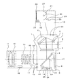
図1は本発明を感光部材として銀塩フィルムを使用する一眼レフレックスカメラに適用した実施例の主に光学的な構成を示す横断面図である。 FIG. 1 is a cross-sectional view mainly showing an optical configuration of an embodiment in which the present invention is applied to a single-lens reflex camera using a silver salt film as a photosensitive member.
1はカメラ本体であり、この中に光学部品、メカ部品、電気回路、フィルムなどが収納され、写真撮影が行えるようになっている。2は主ミラーで、観察状態と撮影状態に応じて撮影光路へ斜設されあるいは退去される。また、主ミラー2はハーフミラーとなっており、斜設されているときも、後述する焦点検出光学系に被写体からの光線の約半分を透過させている。3は撮影レンズ12〜14の予定結像面に配置されたピント板、4はファインダー光路変更用のペンタプリズム、5はファインダー窓で、撮影者はこの窓よりピント板3を観察することで、撮影画面を観察することができる。6,7は観察画面内の被写体輝度を測定するための結像レンズと多分割測光センサで、結像レンズ6はペンタプリズム4内の反射光路を介してピント板3と多分割測光センサ7を共役に関係付けている。
図2に撮影画面上の測光エリア分割図を示す。撮影画面はA1〜A35までの35点の測光エリアに分割されている。多分割測光センサ7は、撮影画面と共役に関係付けられたそれぞれの測光エリアの輝度を測定することができる。 FIG. 2 shows a photometric area division diagram on the photographing screen. The photographing screen is divided into 35 photometric areas A1 to A35. The multi-segment photometric sensor 7 can measure the luminance of each photometric area associated with the imaging screen in a conjugate manner.
図1に戻り、8はシャッター、9は感光部材で、銀塩フィルム等より成っている。21はサブミラーであり、被写体からの光線を下方に折り曲げて、焦点検出ユニット22の方に導いている。焦点検出ユニット22は、2次結像ミラー23、2次結像レンズ24、焦点検出ラインセンサ25等からなっている。2次結像ミラー23及び2次結像レンズ24により焦点検出光学系が形成されており、撮影光学系の2次結像面を焦点検出ラインセンサ25上に結んでいる。焦点検出ユニット22は後述の電気回路の処理によって、既知の位相差検出法により撮影画面内の被写体の焦点状態を検出し、撮影レンズの焦点調節機構を制御することにより自動焦点検出装置を実現している。この自動焦点検出装置は、図2の撮影画面内の各測光エリアの中心点の焦点状態を検出するものである。
Returning to FIG. 1, 8 is a shutter and 9 is a photosensitive member, which is made of a silver salt film or the like.
19は感光部材9のフィルム面を測光するための測光レンズであり、20はフィルム面測光センサである。これらは、露光中にフィルム面に到達した光の拡散反射を利用して露光量を測定し、閃光装置の適正光量を得る、いわゆるTTL(ThroughThe Lens)調光に使用されるものである。
10はカメラ本体1とレンズ鏡筒とのインターフェイスとなるマウント接点であり、11はカメラ本体1に交換可能に取り付けられるレンズ鏡筒である。12〜14は撮影レンズであり、12は1群レンズで、光軸上を可動することで、撮影画面のピント位置を調整することができる。13は2群レンズで、光軸上を可動することで、撮影画面を変倍して、撮影レンズの焦点距離を変更することができる。14は3群固定レンズである。15は絞りである。
16は1群レンズ駆動モータであり、自動焦点調節動作に従って1群レンズ12を光軸方向に前後に移動させることにより自動的にピント位置を調整するものである。17はレンズ絞り駆動モータであり、これにより絞り15を開放にしたり、絞ったりするものである。
18は閃光装置で、カメラ本体1に取り付けられ、カメラ本体1からの信号に従って発光制御を行うものである。26は第1の照明手段である閃光放電管で、電流エネルギーを発光エネルギーに変換するものである。27は反射板、28はフレネルレンズであり、それぞれ発光エネルギーを効率良く被写体に向けて集光する役目のものである。33はカメラ本体1と閃光装置18とのインターフェイスとなる公知の閃光装置接点である。
A
29はグラスファイバーであり、閃光放電管26の発光した光をモニタ用のセンサ(PD1)30に導いている。センサ(PD1)30は閃光装置18のプリ発光及び本発光の光量を直接測光しているものであり、本発光量の制御のためのセンサである。31はやはり閃光放電管26の発光した光をモニタするセンサ(PD2)である。センサ(PD2)31の出力により閃光放電管26の発光電流を制限して閃光装置18はフラット発光を行うことができる。32は第2の照明手段であるR,G,BのLEDであり、34はLED32の照射範囲を調節するためのフレネルレンズである。図1では、本発明の一実施例であるストロボ撮影装置を実現するために必要な部材の内、光学部材及びメカ部材のみを記しており、その他に電気回路が必要となるが、ここでは省略してある。
図3及び図4は本発明の一実施例であるストロボ撮影装置の電気回路を示すブロック図である。図3にはカメラ本体1側とレンズ鏡筒11側の電気回路が示されており、図4には閃光装置18側の電気回路が示されており、それぞれ図1と対応する部材には同じ番号を付している。
3 and 4 are block diagrams showing an electric circuit of a strobe photographing device according to an embodiment of the present invention. FIG. 3 shows an electrical circuit on the
まず、図3から説明する。カメラマイコン100には、焦点検出回路105、測光回路106、シャッター制御回路107、モータ制御回路108、フィルム走行検知回路109、スイッチセンサ回路110、液晶表示回路111、フィルム面反射測光回路114が接続されている。また、レンズ鏡筒11側とはマウント接点10を介して信号の伝達を行う。さらに閃光装置側とは、閃光装置が直接カメラ本体1に取り付けられた状態では、閃光装置接点33を介して信号の伝達を行う。
First, FIG. 3 will be described. Connected to the
焦点検出ラインセンサ25は前述のようにファインダー上の撮影画面内の測光エリアA1〜A35の35点の焦点状態を検出するためのもので、撮影光学系の2次結像面にペアで各測距点に対応したラインセンサである。焦点検出回路105はカメラマイコン100の信号に従い、これら焦点検出ラインセンサ25の蓄積制御と読み出し制御を行って、それぞれ光電変換された画素情報をカメラマイコン100に出力する。カメラマイコン100はこの情報をA/D変換し、周知の位相差検出法による焦点検出を行う。カメラマイコン100は焦点検出情報により、レンズマイコン112と信号のやりとりを行うことによりレンズの焦点調節を行う。
As described above, the focus
測光回路106は撮影画面内の各測光エリアの輝度信号として、前述したように画面内を複数の測光エリアに分割した多分割測光センサ7からの出力をカメラマイコン100に出力する。測光回路106は、被写体に向けて閃光装置18がプリ発光していない定常状態とプリ発光しているプリ発光状態との双方の状態で輝度信号を出力し、カメラマイコン100は輝度信号をA/D変換し、撮影の露出調節のための絞り値の演算とシャッタースピードの演算、及び露光時の閃光装置18の本発光量の演算を行う。
The
シャッター制御回路107は、カメラマイコン100からの信号に従って、シャッター先幕(MG−1)、シャッター後幕(MG−2)を走行させ、露出動作を担っている。
The
モータ制御回路108は、カメラマイコン100からの信号に従ってモータを制御することにより、主ミラー2のアップダウン、及びシャッター8のチャージ、そしてフィルムの給送を行っている。フィルム走行検知回路109は、フィルム給送時にフィルムが1駒分巻き上げられたか否かを検知し、カメラマイコン100に信号を送る。
The
SW1は不図示のレリーズ釦の第1ストロークでオンし、測光、AFを開始するスイッチである。SW2はレリーズ釦の第2ストロークでオンし、露光動作を開始するスイッチである。SWFELKは、不図示のプッシュスイッチでオンするスイッチであり、露光動作の前に閃光装置18のプリ発光を行って閃光装置18の光量を決定し、ロックする動作の始動スイッチである。SW1,SW2,SWFELK及びその他不図示のカメラの操作部材からの信号は、スイッチセンサ回路110が検知し、カメラマイコン100に送っている。SWXは、シャッターの全開にともなってオンするスイッチであり、閃光装置18側に、露光時本発光の発光タイミングを送っている。
SW1 is a switch that is turned on by a first stroke of a release button (not shown) and starts photometry and AF. SW2 is a switch that is turned on by the second stroke of the release button and starts an exposure operation. SWFELK is a switch that is turned on by a push switch (not shown), and is a start switch for performing an operation of performing pre-light emission of the
液晶表示回路111はファインダー内LCD41とモニタ用LCD42の表示をカメラマイコン100からの信号に従って制御している。114はフィルム面反射測光回路であり、フィルム面測光センサ20の測光情報をカメラマイコン100は得ることができる。このフィルム面測光センサ20は、多分割測光センサ7と同様に図2のように撮影画面内が多数の測光エリアに分割されたものであり、撮影画面と共役に関係付けられたそれぞれの測光エリアの輝度を測定することができる。
The liquid
次にレンズ鏡筒11の構成に関して説明する。カメラ本体1とレンズ鏡筒11はマウント接点10を介して相互に電気的に接続される。このマウント接点10はレンズ鏡筒11内のフォーカス駆動モータ16及び絞り駆動モータ17の電源用接点であるL0、レンズマイコン112の電源用接点であるL1、公知のシリアルデータ通信を行うためのクロック用接点L2、カメラ本体1からレンズ鏡筒11へのデータ送信用接点L3、レンズ鏡筒11からカメラ本体1へのデータ送信用接点L4、前記モータ用電源に対するモータ用グランド接点であるL5、前記レンズマイコン112用電源に対するグランド接点であるL6で構成されている。
Next, the configuration of the
レンズマイコン112は、これらのマウント接点10を介してカメラマイコン100と接続され、フォーカス駆動モータ16及び絞り駆動モータ17を動作させ、1群レンズ12の焦点調節と絞り15を制御している。35,36は光検出器とパルス板であり、レンズマイコン112がパルス数をカウントすることにより1群レンズ12の位置情報を得ることができ、1群レンズ12の焦点調節を行ったり、被写体の絶対距離情報をカメラマイコン100に伝達したりすることができる。
The
環境光判定回路113は、測光回路106により得られた信号から測光エリア毎に色評価値Cx、Cyを下記の式(1)〜(3)に基づいて算出する。
The ambient
Y=(R+G+B)/2 …(1)
Cx=(R−B)/Y …(2)
Cy=(R+B−2G)/Y …(3)
上記の式(1)〜(3)により算出した各測光エリアの色評価値Cx、Cyをあらかじめ設定した後述する環境光検出領域と比較し、各測光エリアでどのような環境光が支配的であるかを判定する。なお、どの環境光が支配的であるかということは、被写体からの反射光の中でどの環境光の成分が最も大きいかということを意味している。
Y = (R + G + B) / 2 (1)
Cx = (R−B) / Y (2)
Cy = (R + B-2G) / Y (3)
The color evaluation values Cx and Cy of each photometry area calculated by the above formulas (1) to (3) are compared with an environment light detection area described later which is set in advance, and what kind of environmental light is dominant in each photometry area. Determine if there is . Note that which environmental light is dominant means which environmental light component is the largest among the reflected light from the subject.
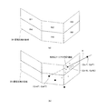
図7は、環境光検出領域301を示すグラフである。この環境光検出領域301を求めるには、高色温度から低色温度まで、任意の色温度間隔の光源を用いて不図示の基準白色板などの白色被写体を測光し、測光回路106から得られた信号値より式(1)〜(3)に基づいて色評価値Cx、Cyを算出する。そして、それぞれの光源について得られたCxをX軸、CyをY軸としてプロットしたものを直線で結ぶか、プロットした点を複数の直線を用いて近似する。これにより、高色温度から低色温度までの環境光検出軸302が作成される。実際にはさまざまな環境光に対応するために、環境光検出軸302に対してY軸方向に若干の幅を持たせたものを環境光検出領域301と定義する。例えば、タングステン光、白色蛍光灯はこのCx−Cy平面上においては、タングステン光領域303、白色蛍光灯領域304にプロットされる。
FIG. 7 is a graph showing the ambient light detection region 301. In order to obtain the ambient light detection region 301, a white object such as a reference white plate (not shown) is measured using a light source having an arbitrary color temperature interval from a high color temperature to a low color temperature, and obtained from the
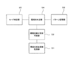
図8は環境光判定回路113の概略構成を示す測光エリア図である。同図において、50は撮影装置の動作モード(オートモード、人物を撮影する人物撮影モード、風景を撮影する風景撮影モードなど)を判定するモード判定部、51は基準となる環境光検出領域(以下、「基準環境光検出領域」と呼ぶ)を記憶する環境光検出領域記憶部、52は環境光検出領域をリミット値を用いて適宜変更する環境光検出領域可変部、53は撮影画面上の位置及びその位置にある測光エリアの色評価値を記憶するパターン記憶部、54は各測光エリアにおいてどのような環境光が支配的であるかを判定する環境光判定部である。環境光判定部54はモード判定部50の判定結果に応じて環境光検出領域301を変化させる。例えば、屋外での撮影を想定している風景撮影モードでは、環境光が環境光検出軸302に近い領域にプロットされる確率が高いため環境光検出領域301のY軸方向の幅を小さくし、人物が撮影画面内を占める割合が大きくなる人物撮影モードでは、環境光検出領域301のY軸方向の幅を大きくする。このようにすることで、環境光の誤検出の確率を低減させることができる。
FIG. 8 is a photometric area diagram showing a schematic configuration of the ambient
次に図4により、閃光装置18の構成に関して説明する。
Next, the configuration of the
閃光装置マイコン200はカメラマイコン100からの信号に従って、閃光装置18の制御を行う回路で、発光量の制御、プリ発光の発光強度及び発光時間の制御等を行う。201は、DC/DCコンバータで、閃光装置マイコン200の指示により電池電圧を数百Vに昇圧し、主コンデンサC1に充電する。R1,R2は、主コンデンサC1の電圧を閃光装置マイコン200がモニタするために設けられた分圧抵抗である。閃光装置マイコン200は、分圧された電圧を閃光装置マイコン200に内蔵されたA/D変換器によりA/D変換して、主コンデンサC1の電圧を間接的にモニタし、DC/DCコンバータ201の動作を制御することにより、主コンデンサC1の電圧を所定の電圧に制御する。
The
202は既存のトリガ回路で、閃光装置発光時にカメラマイコン100の指示やSWX信号により閃光装置マイコン200を介してトリガ信号を出力し、閃光放電管26のトリガ電極に数千Vの高電圧を印加することにより閃光放電管26の放電を誘発し、主コンデンサC1に蓄えられた電荷エネルギーを閃光放電管26を介して光エネルギーとして放出させる。203はIGBT(InsulatedGate Bipolar Transistor)等のスイッチング素子を用いた既存の発光制御回路であり、前記発光時のトリガ電圧印加時には導通状態とし、閃光放電管26の電流を流し、発光停止時には遮断状態にすることにより、閃光放電管26の電流を遮断し、発光を停止させる。204,205はコンパレータである。206はデータセレクタで、閃光装置マイコン200からの選択信号SEL0、SEL1に従い、X0からX2の入力を選択し、Yに出力する。
An existing
207は閃光発光制御用モニタ回路であり、センサ(PD1)30の出力を増幅する。208は閃光発光制御用モニタ回路207の出力を積分する積分回路である。209はフラット発光制御用モニタ回路であり、センサ(PD2)31の出力を増幅する。210は前記フラット発光時間等を記憶する記憶手段であるEEPROMである。211は発光可能かどうかの状態を示すLEDである。32R、32G、32Bは第2の照明手段であるR,G,BのLEDであり、アノードは電源である電池(battery)と接続され、カソードは既存の定電流回路37,38,39と接続されている。
213はR,G,BのLED32の発光量の比に対応した色温度テーブルを保持している不揮発性メモリ(EEPROM)である。
次に閃光装置マイコン200の各端子の説明をする。
Next, each terminal of the
CKはカメラマイコン100とのシリアル通信を行うための同期クロックの入力端子、DIはシリアル通信データの入力端子、DOはシリアル通信のデータ出力端子、CHGは閃光装置18の発光可能状態を電流の形でカメラマイコン100に伝える出力端子、Xはカメラマイコン100からの発光タイミング信号の入力端子、ECKはフラッシュROM等の書き込み可能な記憶手段とシリアル通信を行うための通信クロックを出力する出力端子、EDIは前記記憶手段からのシリアル通信データ入力端子、EDOは前記記憶手段へのシリアルデータ出力端子、SELEは記憶手段との通信を許可するイネーブル端子であり、説明上Loでイネーブル、Hiでディスエーブルとする。
CK is an input terminal of a synchronous clock for performing serial communication with the
POWはパワースイッチ212の状態を入力する入力端子、OFFはパワースイッチ212と接続された時に閃光装置18をオフ状態にするための出力端子、ONはパワースイッチ212と接続された時の閃光装置18をオン状態にするための出力端子であり、パワーオン状態ではPOW端子はON端子と接続され、その際ON端子はハイインピーダンス状態、OFF端子はLo状態であり、パワーオフ状態ではその逆である。LEDは発光可能を表示する表示出力端子である。
POW is an input terminal for inputting the state of the
STOPは発光停止信号の入力端子であり、説明上Loで発光停止状態とする。SEL0、SEL1は前記データセレクタ206の入力選択を指示するための出力端子であり、SEL0、SEL1の組み合わせが(SEL1,SEL0)=(0,0)の時はX0端子がY端子に接続され、同様に(0,1)の時はX1端子が、(1,0)の時はX2端子が、それぞれ選択される。
STOP is an input terminal for a light emission stop signal. For the sake of explanation, the light emission stop state is set to Lo. SEL0 and SEL1 are output terminals for instructing the input selection of the
DA0は閃光装置マイコン200に内蔵されたD/A出力端子であり、コンパレータ204,205のコンパレートレベルをアナログ電圧で出力する。TRIGはトリガ回路202に発光を指示するトリガ信号出力端子である。CNTはDC/DCコンバータ201の発振開始停止を制御する出力端子で、説明上Hiで充電開始、Loで充電停止とする。INTは積分回路208の積分の開始/リセットを制御する端子で、Hiで積分リセット、Loで積分許可とする。
DA0 is a D / A output terminal built in the
AD0、AD1はA/D入力端子であり、入力される電圧を閃光装置マイコン200内部で処理できるようにディジタルデータに変換するものであり、AD0は主コンデンサC1の電圧をモニタするものであり、AD1は積分回路208の積分出力電圧をモニタするものである。
AD0 and AD1 are A / D input terminals, which convert input voltages into digital data so that they can be processed inside the
定電流回路37,38,39は閃光装置マイコン200のLED_P端子がHiの時、閃光装置マイコン200の内蔵D/Aコンバータ出力のDAR,DAG,DAB端子から出力される電圧に応じた定電流駆動でLED32R,32G,32Bを点灯させる。
When the LED_P terminal of the
次に、この閃光装置のそれぞれの動作を図4を用いて説明する。 Next, each operation | movement of this flash device is demonstrated using FIG.
(発光可能状態検知)
閃光装置マイコン200は、AD0端子に入力された主コンデンサC1の分圧された電圧をA/D変換することによって、主コンデンサC1の電圧が発光可能な所定電圧以上であると判別すると、CHG端子より所定電流を吸い込み、カメラマイコン100に発光可能を伝える。また、LED端子をHiに設定し、LED211を発光させて、発光可能状態であることを表示する。主コンデンサC1の電圧が所定電圧以下であると判別したときは、CHG端子をノンアクティブに設定するので、電流は遮断され、カメラマイコン100には発光不能が伝わる。また、LED端子をLoに設定し、LED211を消灯させて、発光不能を表示する。
(Light emission enabled state detection)
When the
(閃光放電管26(第1の照明手段)によるプリ発光)
閃光装置が発光可能状態のとき、カメラ本体1は、プリ発光の発光強度と発光時間を通信すると共に、閃光放電管26(第1の照明手段)によるプリ発光を指示することができる。閃光放電管26(第1の照明手段)をほぼ一定の発光強度で発光継続させるフラット発光によるプリ発光動作を以下に説明する。
(Pre-emission by the flash discharge tube 26 (first illumination means))
When the flash device is ready to emit light, the
閃光装置マイコン200は、カメラ本体1より指示された所定発光強度信号に応じて、DA0端子に所定のコンパレートレベルを設定する。次にSEL1端子、SEL0端子にLo、Hiを出力し、入力X1を選択する。このとき閃光放電管26はまだ発光していないので、センサ(PD2)31の光電流はほとんど流れず、コンパレータ205の反転入力端子に入力されるフラット発光制御用モニタ回路209の出力は発生せず、コンパレータ205の出力はHiであるので、発光制御回路203は導通状態となる。次にTRIG端子よりトリガ信号を出力すると、トリガ回路202は高圧を発生し、閃光放電管26を励起し、発光が開始される。
The
一方、閃光装置マイコン200は、トリガ発生より所定時間後、積分回路208に積分開始を指示し、積分回路208は閃光発光制御用モニタ回路207の出力、すなわち、光量積分用のセンサ(PD1)30の光電出力を積分開始すると同時に、所定時間をカウントするタイマを起動させる。
On the other hand, the
プリ発光が開始されると、フラット発光強度制御用のセンサ(PD2)31の光電流が多くなり、フラット発光制御用モニタ回路209の出力が上昇し、コンパレータ205の非反転入力に設定されている所定のコンパレートレベルより高くなると、コンパレータ205の出力はLoに反転し、発光制御回路203は閃光放電管26の発光電流を遮断し、放電ループを断つが、ダイオードD1、コイルL1により環流ループが形成されて、発光電流は回路の遅れによるオーバーシュートが収まった後は、徐々に減少する。発光電流の減少に伴い、発光強度が低下するので、センサ(PD2)31の光電流は減少し、フラット発光制御用モニタ回路209の出力は低下し、所定のコンパレートレベル以下に低下すると、再びコンパレータ205の出力はHiに反転し、発光制御回路203が再度導通し、閃光放電管26の放電ループが形成され、発光電流が増加し、発光強度も増加する。このように、DA0端子に設定された所定のコンパレートレベルを中心に、コンパレータ205は短い周期で発光強度の増加減少を繰り返し、結果的には、所望するほぼ一定の発光強度で発光を継続させるフラット発光の制御ができる。
When pre-emission is started, the photocurrent of the flat emission intensity control sensor (PD2) 31 increases, the output of the flat emission
前述の発光時間タイマによりプリ発光時間をカウントし、所定のプリ発光時間が経過すると、閃光装置マイコン200はSEL1端子、SEL0端子をLo、Loに設定し、データセレクタ206の入力としてX0すなわちLo入力が選択され、出力は強制的にLoとなり、発光制御回路203は閃光放電管26の放電ループを遮断し、発光を終了させる。
The pre-emission time is counted by the above-described emission time timer, and when the predetermined pre-emission time elapses, the
発光終了時に、閃光装置マイコン200は、プリ発光を積分した積分回路208の出力をAD1端子から読み込み、A/D変換し、積分値、すなわちプリ発光時の発光量をディジタル値(INTp)として読みとることができる。
At the end of light emission, the
(本発光制御)
カメラマイコン100は、プリ発光時の多分割測光センサ7からの被写体反射光輝度値等から、本発光量のプリ発光量に対する適正相対値(γ)を求め、閃光装置マイコン200に送る。
(Main flash control)
The
閃光装置マイコン200は、プリ発光時の積分値(INTp)にカメラマイコン100からの相対値(γ)の値を掛け合わせて適正積分値(INTm)を求め、DA0出力に適正積分値(INTm)を設定する。
The
次にSEL1端子、SEL0端子にHi、Loを出力し、入力X2を選択する。このとき、積分回路208は動作禁止状態なので、コンパレータ204の反転入力端子に入力される積分回路208の出力は発生せず、コンパレータ204の出力はHiであるので、発光制御回路203は導通状態となる。次にTRIG端子よりトリガ信号を出力すると、トリガ回路202は高圧を発生し、閃光放電管26を励起し、発光が開始される。また、閃光装置マイコン200は、トリガ信号印加によるトリガノイズが収まるとともに実際の発光が開始される10数μsec後に積分開始端子INTをLoに設定し、積分回路208はセンサ(PD1)30からの出力を閃光発光制御用モニタ回路207を介して積分する。積分出力がDA0端子で設定された所定電圧に到達すると、コンパレータ204は反転し、データセレクタ206の制御により発光制御回路203は放電ループを遮断し、発光は停止する。一方、閃光装置マイコン200はSTOP端子をモニタし、STOP端子が反転し、発光が停止すると、SEL1端子、SEL0端子をLo、Loに設定し、強制発光禁止状態に設定するとともに、INT端子を反転し、積分を終了し、発光処理を終了する。このようにして、本発光量を適正な発光量に制御することができる。
Next, Hi and Lo are output to the SEL1 terminal and the SEL0 terminal, and the input X2 is selected. At this time, since the
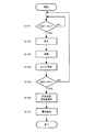
次に、図5及び図6を用いて本発明の一実施例であるストロボ撮影装置の動作フローをカメラマイコン100の動作を中心に説明する。 Next, the operation flow of the strobe photographing apparatus according to the embodiment of the present invention will be described with reference to FIGS.
図5においてカメラ動作が開始されると、カメラマイコン100はまずレリーズ釦の第1ストロークでオンするスイッチSW1のオンを検出する(ステップS101)。スイッチSW1のオンが検出されるまではこのステップが繰り返し実行される。
When the camera operation is started in FIG. 5, the
スイッチSW1のオンが検出されると、カメラマイコン100は、測光回路106より撮影画面内の複数の測光エリアの被写体輝度情報、色情報をA/D変換により得る(ステップS102)。この輝度情報により、後述での露光動作に用いるシャッタースピード、絞り値を演算により求める。
When it is detected that the switch SW1 is turned on, the
次に、カメラマイコン100は焦点検出回路105を駆動することにより周知の位相差検出法による焦点検出動作を行う(ステップS103)。焦点を検出するポイント(測距ポイント)は前述したように複数あるため、撮影者が任意に測距ポイントを設定できる方式の場合と、近点優先を基本の考え方とした周知の自動選択アルゴリズム方式の場合等がある。
Next, the
選択された測距ポイントが合焦となるように、カメラマイコン100はレンズマイコン112と通信を行うことによって1群レンズ12の焦点調節を行う(ステップS104)。また、レンズ合焦位置の絶対距離情報を通信によってカメラマイコン100は得ることができる。
The
ここで、カメラマイコン100は、レリーズ釦の第2ストロークでオンするスイッチSW2がオンであるかどうかを判別する(ステップS105)。スイッチSW2がオフであれば、ステップS101〜S105の動作を繰り返し、スイッチSW2がオンであれば、レリーズ動作に進む。
Here, the
レリーズ動作に入ると、まず、閃光装置発光量演算サブルーチンをコールする(ステップS106)。 When the release operation is started, first, a flash device emission amount calculation subroutine is called (step S106).
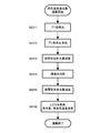
ここで、閃光装置発光量演算サブルーチンを、図6を用いて説明する。 Here, the flash device emission amount calculation subroutine will be described with reference to FIG.
測光回路106のプリ前測光により得られる輝度値をそれぞれの測光エリア毎、R,G,Bの信号毎にEvRa(i),EvGa(i),EvBa(i)とすると、i=1〜35にて、
Ra(i)=2^{EvRa(i)} …(4)
Ga(i)=2^{EvGa(i)} …(5)
Ba(i)=2^{EvBa(i)} …(6)
としてRAMに記憶させる(ステップS201)。
Assuming that the luminance value obtained by the pre-photometry of the
Ra (i) = 2 ^ {EvRa (i)} (4)
Ga (i) = 2 ^ {EvGa (i)} (5)
Ba (i) = 2 ^ {EvBa (i)} (6)
Is stored in the RAM (step S201).
さらに、上記の輝度値を用いて、各測光エリアにおける色評価値Cxa、Cyaを下記の式(7)〜(9)により算出する。 Further, the color evaluation values Cxa and Cya in each photometry area are calculated by the following formulas (7) to (9) using the luminance value.
Ya(i)={Ra(i)+Ga(i)+Ba(i)}/2 …(7)
Cxa(i)={Ra(i)−Ba(i)}/Ya(i) …(8)
Cya(i)={Ra(i)+Ba(i)−2Ga(i)}/Ya(i) …(9)
次に、カメラマイコン100は、閃光装置18側に対してプリ発光の命令を行う。閃光装置マイコン200はこの命令に従って、前述したようにプリ発光動作を行い、プリ発光が持続している間に被写体からの反射光を測光回路106により得る。その輝度値をそれぞれの測光エリア毎、R,G,Bの信号毎にEvRf(i),EvGf(i),EvBf(i)とすると、
Rf(i)=2^{EvRf(i)} …(10)
Gf(i)=2^{EvGf(i)} …(11)
Bf(i)=2^{EvBf(i)} …(12)
としてRAMに記憶させる(ステップS202)。
Ya (i) = {Ra (i) + Ga (i) + Ba (i)} / 2 (7)
Cxa (i) = {Ra (i) -Ba (i)} / Ya (i) (8)
Cya (i) = {Ra (i) + Ba (i) -2Ga (i)} / Ya (i) (9)
Next, the
Rf (i) = 2 ^ {EvRf (i)} (10)
Gf (i) = 2 ^ {EvGf (i)} (11)
Bf (i) = 2 ^ {EvBf (i)} (12)
Is stored in the RAM (step S202).
さらに、上記の輝度値を用いて、各測光エリアにおける色評価値Cxf、Cyfを下記の式(13)〜(15)により算出する。 Further, the color evaluation values Cxf and Cyf in each photometric area are calculated by the following formulas (13) to (15) using the luminance value.
Yf(i)={Rf(i)+Gf(i)+Bf(i)}/2 …(13)
Cxf(i)={Rf(i)−Bf(i)}/Yf(i) …(14)
Cyf(i)={Rf(i)+Bf(i)−2Gf(i)}/Yf(i) …(15)
ステップS201,S202で求めた反射光量から、プリ発光反射光分のみの輝度値を抽出する。
Yf (i) = {Rf (i) + Gf (i) + Bf (i)} / 2 (13)
Cxf (i) = {Rf (i) -Bf (i)} / Yf (i) (14)
Cyf (i) = {Rf (i) + Bf (i) -2Gf (i)} / Yf (i) (15)
From the amount of reflected light obtained in steps S201 and S202, a luminance value only for the pre-emission reflected light is extracted.
EvdRf(i)←EvRf(i)−EvRa(i) …(16)
EvdGf(i)←EvGf(i)−EvGa(i) …(17)
EvdBf(i)←EvBf(i)−EvBa(i) …(18)
これらの輝度値をRAMに記憶させる(ステップS203)。
EvdRf (i) ← EvRf (i) −EvRa (i) (16)
EvdGf (i) ← EvGf (i) −EvGa (i) (17)
EvdBf (i) ← EvBf (i) −EvBa (i) (18)
These luminance values are stored in the RAM (step S203).
上記の式(13)〜(15)により求めた各測光エリアにおける色評価値Cxf、CyfをCx−Cy軸からなる2次元の座標上にプロットする。ここで、プリ測光時に得た輝度値とプリ前測光時に得た画面全体の輝度値の平均値との差が所定値以上である測光エリアは、画面全体の支配的な環境光とは異なる別の環境光が照射されているとみなし、該当する測光エリアについては除外して以下に示す主たる環境光の色評価値の演算を行う。ここで、画面全体の支配的な主たる環境光とは、被写界全体に照明されている太陽光や蛍光灯の光などを指し、画面全体の支配的な環境光とは異なる別の環境光とは、閃光装置の閃光放電管26の光を指す。このようにすることで、第2の照明手段によって誤って被写体色を打ち消してしまう確率を減らすことができる。図9(a)に示すR1〜R6の領域内に含まれる色評価値の測光エリアの個数をカウントし、個数が最も多い領域内の測光エリア毎のR,G,Bの輝度値を積分や平均化などして、式(13)〜(15)を用いて、プリ発光時において画面全体で最も支配的な主たる環境光の色評価値CxfS、CyfSを演算する(ステップS204)。あるエリアに他の部分とは異なる別の環境光が照射されている場合、そのエリアの輝度値は他のエリアと比べて高くなっていると考えられる(主たる環境光の輝度+別の環境光の輝度の和が得られるため)。上記の演算では、輝度値の高いエリアについては除外して色評価値を算出しているので、画面全体において最も支配的な主たる環境光の色評価値を求めることができる。
The color evaluation values Cxf and Cyf in each photometric area obtained by the above formulas (13) to (15) are plotted on the two-dimensional coordinates composed of the Cx-Cy axes. Here, the metering area where the difference between the brightness value obtained during pre-metering and the average value of the whole screen brightness obtained during pre-metering is greater than or equal to a predetermined value is different from the dominant ambient light of the entire screen. Therefore, the corresponding light metering area is excluded, and the color evaluation value of the main ambient light shown below is calculated. Here, the dominant main ambient light of the entire screen refers to sunlight or fluorescent light illuminating the entire object field, which is different from the dominant ambient light of the entire screen. Refers to the light from the
次に、プリ前測光およびプリ発光時の輝度情報、測距情報等を基に公知の手法を用いて適正露出値を算出する(ステップS205)。 Next, an appropriate exposure value is calculated using a known technique based on pre-pre-photometry, luminance information at the time of pre-emission, distance measurement information, and the like (step S205).
ステップS206では、画面全体において最も支配的な主たる環境光とは異なる別の環境光が支配的な領域を求め、その領域に対してR,G,BのLEDを発光させる。画面全体のプリ前測光時の輝度値の平均値をEvAvgR,EvAvgG,EvAvgBとすると、以下の値CThが所定値以上の測光エリアは、画面全体において最も支配的な主たる環境光とは異なる別の環境光が支配的であるものとする。 In step S206, a region in which another ambient light different from the most dominant main ambient light is dominant in the entire screen is obtained, and R, G, and B LEDs are caused to emit light in the region. Assuming that the average value of the luminance values during pre- pre- metering of the entire screen is EvAvgR, EvAvgG, and EvAvgB, a photometric area in which the following value CTh is equal to or greater than a predetermined value is different from the most dominant main environmental light in the entire screen. Ambient light shall be dominant.
CTh=k1×EvAvgd(i)+ k2×CAvgd(i) …(19)
EvAvgd={EvAvgR−EvRf(i)}^2+{EvAvgG−EvGf(i)}^2+ {EvAvgB−EvBf(i)}^2 …(20)
CAvgd(i)={CxfS−Cxf(i)}^2+{CyfS−Cyf(i)}^2 …(21)
k1,k2は輝度差、色評価値差に対して重み付けを行う係数である。
CTh = k1 * EvAvgd (i) + k2 * CAvgd (i) (19)
EvAvgd = {EvAvgR-EvRf (i)} ^ 2+ {EvAvgG-EvGf (i)} ^ 2+ {EvAvgB-EvBf (i)} ^ 2 (20)
CAvgd (i) = {CxfS-Cxf (i)} ^ 2+ {CyfS-Cyf (i)} ^ 2 (21)
k1 and k2 are coefficients for weighting the luminance difference and the color evaluation value difference.
LED32を発光させずに閃光放電管26のみで適正露出値を得たときの輝度値をEvRT、EvGT、EvBTとすると、そのときの色評価値CxdT、CydTは下記の式(22)〜(28)で算出される。
Assuming that the luminance values when the appropriate exposure value is obtained only by the
EvRT(i)=EvRa(i)+kR×(EvRf(i)−EvRa(i))…(22)
EvGT(i)=EvGa(i)+kG×(EvGf(i)−EvGa(i))…(23)
EvBT(i)=EvBa(i)+kB×(EvBf(i)−EvBa(i))…(24)
RdT(i)=2^EvRT(i),GdT(i)=2^EvGT(i),BdT(i)=2^EvBT(i) …(25)
YdT(i)=(RdT(i)+GdT(i)+BdT(i))/2 …(26)
CxdT(i)=(RdT(i)−BdT(i))/YdT(i) …(27)
CydT(i)=(RdT(i)+BdT(i)−2GdT(i))/YdT(i) …(28)
ここで、kR,kG,kBは環境光成分とプリ発光成分の比より決まる値である。
EvRT (i) = EvRa (i) + kR × (EvRf (i) −EvRa (i)) (22)
EvGT (i) = EvGa (i) + kG × (EvGf (i) −EvGa (i)) (23)
EvBT (i) = EvBa (i) + kB × (EvBf (i) −EvBa (i)) (24)
RdT (i) = 2 ^ EvRT (i), GdT (i) = 2 ^ EvGT (i), BdT (i) = 2 ^ EvBT (i) (25)
YdT (i) = (RdT (i) + GdT (i) + BdT (i)) / 2 (26)
CxdT (i) = (RdT (i) −BdT (i)) / YdT (i) (27)
CydT (i) = (RdT (i) + BdT (i) -2GdT (i)) / YdT (i) (28)
Here, kR, kG, and kB are values determined by the ratio of the ambient light component and the pre-light emission component.
次に、CThが所定値以上の測光エリアの(CxdT(i),CydT(i))を上記式(27)、(28)より求め、これらの平均値である(CxdT,CydT)を用いてR,G,BのLED32の発光量および各LED32の発光量比を求める。図9(b)より、LED32の発光の色評価値は(CxdT,CydT)と(CxfS,CyfS)を結ぶ直線の延長線X上であって、かつ(CxfS,CyfS)を境として(CxdT,CydT)と反対側に位置すればよい。延長線X上にあるR,G,BのLED32の発光量の比の組み合わせをEEPROM213から存在するだけ読み出す。複数読み込まれた発光量の比の組み合わせのうち、LED照射による露出への影響が最も小さくて済む、つまり(CxfS,CyfS)から最も遠い点の色評価値(CxlT,CylT)の発光量の比の組み合わせを選択する。このようにすることで、閃光放電管26による照明が行われている状況下で、主たる環境光とは異なる別の環境光が照射されている領域の色温度が主たる環境光が照射されている領域の色温度に近づくようにLED32を照射することが可能になる。
Next, (CxdT (i), CydT (i)) of the photometric area where CTh is equal to or larger than a predetermined value is obtained from the above equations (27) and (28), and the average value of these (CxdT, CydT) is used. The light emission amount of the R, G,
ここで閃光装置発光量演算サブルーチンを終え、図5に戻り、カメラマイコン100は、露光動作を行う(ステップS107)。すなわち、主ミラー2をアップさせ、サブミラー25ともども撮影光路より退去させ、絞り駆動モータ17により絞り15を制御し、決められたシャッタースピード値(TV)になるようにシャッター制御回路107を制御する。このとき、シャッター8の全開に同期してスイッチSWXがオンし、閃光装置18側に伝わり、これが本発光の命令となる。閃光装置マイコン200は、カメラマイコン100から送られてきた適正相対値γに基づいて前述のような本発光制御を行う。LED32はシャッター8が開く前に選択された発光量の比の組み合わせに応じた発光を開始しており、LED32による発光は閃光放電管26による発光が行われている間も維持されている。
Here, the flash device emission amount calculation subroutine is finished, and the processing returns to FIG. 5 and the
最後に、撮影光路より退去された主ミラー2等をダウンし、再び撮影光路へ斜設させ、モータ制御回路108とフィルム走行検知回路109により、フィルムを1駒巻き上げる。
Finally, the main mirror 2 and the like moved away from the photographing optical path are lowered and obliquely installed in the photographing optical path again, and the film is wound up by the
上記の実施例によれば、主たる環境光とは異なる別の環境光が支配的である領域に対して、主たる環境光が支配的である領域と同様の色味になるようにR,G,Bの発光量の比を調節してLED32を照射し、撮影画面内での色再現を同じ様にすることで、画像が不自然にならないようなストロボ撮影装置を提供することができる。また、LED32により撮影画面内の一部を照射するようにして、照射エネルギーを集中させることができるため、LED32でも十分な光量を得ることができる。
According to the above-described embodiment, R, G, and R have colors similar to those in the region where the main environment light is dominant, with respect to the region where another environment light different from the main environment light is dominant. By adjusting the ratio of the light emission amount of B and irradiating the
実施例では感光部材9として銀塩フィルムを使用しているが、CCD(Charge−CoupledDevices)やCMOS(Complementary Metal−Oxide Semiconductor)等の光電変換素子からなる撮像素子を用いることができる。 In the embodiment, a silver salt film is used as the photosensitive member 9, but an image pickup element such as a CCD (Charge-Coupled Devices) or a CMOS (Complementary Metal-Oxide Semiconductor) can be used.
また、実施例では図6の閃光装置発光量演算サブルーチンをカメラマイコン100が実行しているが、閃光装置マイコン200が実行するようにしてもよい。
In the embodiment, the flash device light emission amount calculation subroutine of FIG. 6 is executed by the
また、本発明はビデオカメラにも適用することができる。この場合には、閃光放電管26の代わりに連続発光を行う照明手段を使用する。
The present invention can also be applied to a video camera. In this case, instead of the
さらに、閃光放電管26やLED32はカメラ本体に内蔵されていても構わない。
Further, the
1 カメラ本体
2 主ミラー
3 ピント板
4 ペンタプリズム
5 ファインダー
6 結像レンズ
7 多分割測光センサ
8 シャッター
9 感光部材
10 マウント接点
11 レンズ鏡筒
12 1群レンズ
13 2群レンズ
14 3群固定レンズ
15 絞り
16 1群レンズ駆動モータ
17 レンズ絞り駆動モータ
18 閃光装置
19 測光レンズ
20 フィルム面測光センサ
21 サブミラー
22 焦点検出ユニット
23 2次結像ミラー
24 2次結像レンズ
25 焦点検出ラインセンサ
26 閃光放電管
27 反射板
28 フレネルレンズ
29 グラスファイバー
30,31 センサ
32 R,G,Bの発光ダイオード
33 閃光装置接点
41 ファインダー内LCD
42 モニタ用LCD
100 カメラマイコン
100a EEPROM
100b A/D変換器
106 測光回路
107 シャッター制御回路
108 モータ制御回路
109 フィルム走行検知回路
111 液晶表示回路
112 レンズマイコン
113 環境光判定回路
114 フィルム面反射測光回路
201 DC/DCコンバータ
202 トリガ回路
203 発光制御回路
204,205 コンパレータ
206 データセレクタ
207 閃光発光制御用モニタ回路
208 積分回路
209 フラット発光制御用モニタ回路
210,213 EEPROM
211 発光ダイオード
212 パワースイッチ
DESCRIPTION OF
42 LCD for monitor
100
100b A /
211 Light-emitting
Claims (6)
互いの発光量比を変更できる複数色の光源を有する第2の照明手段と、
撮影画面内の複数の領域における被写体輝度を測定する輝度測定手段と、
前記複数の領域の色評価値を求める評価手段と、
前記第1の照明手段のみを発光させたときに前記輝度測定手段により測光を行って得られた輝度値である第1の輝度値と前記第1の照明手段及び前記第2の照明手段を発光させていないときに前記輝度測定手段により測光を行って得られた輝度値である第2の輝度値との差に基づく値が所定値以上である領域の色評価値に基づく第1の色評価値と、前記第1の輝度値と前記第2の輝度値との差に基づく値が所定値未満である領域の色評価値に基づく第2の色評価値との差を補償するような光量比で、前記第2の照明手段を発光させる制御手段と、を有することを特徴とする照明撮影装置。 First illumination means;
A second illuminating means having a light source of a plurality of colors capable of changing the light emission amount ratio of each other;
Luminance measuring means for measuring subject luminance in a plurality of areas in the shooting screen;
Evaluation means for obtaining color evaluation values of the plurality of regions;
When only the first illumination unit emits light, the first luminance value, which is a luminance value obtained by performing photometry with the luminance measurement unit, and the first illumination unit and the second illumination unit emit light. A first color evaluation based on a color evaluation value of an area in which a value based on a difference from a second luminance value, which is a luminance value obtained by performing photometry with the luminance measuring means when not measured, is a predetermined value or more A quantity of light that compensates for a difference between a value and a second color evaluation value based on a color evaluation value of an area where the value based on the difference between the first luminance value and the second luminance value is less than a predetermined value And a control means for causing the second illumination means to emit light at a ratio.
撮影画面内の複数の領域における被写体輝度を測定する輝度測定手段と、
前記複数の領域の色評価値を求める評価手段と、
前記第1の照明手段のみを発光させたときに前記輝度測定手段により測光を行って得られた輝度値である第1の輝度値と前記第1の照明手段及び前記第2の照明手段を発光させていないときに前記輝度測定手段により測光を行って得られた輝度値である第2の輝度値との差に基づく値が所定値以上である領域の色評価値に基づく第1の色評価値と、前記第1の輝度値と前記第2の輝度値との差に基づく値が所定値未満である領域の色評価値に基づく第2の色評価値との差を補償するような光量比を求め、前記第2の照明手段が当該光量比で発光するように制御する制御手段と、を有することを特徴とする撮影装置。 An imaging device for controlling a first illumination unit and a second illumination unit having a plurality of color light sources capable of changing a light emission amount ratio of each other,
Luminance measuring means for measuring subject luminance in a plurality of areas in the shooting screen;
Evaluation means for obtaining color evaluation values of the plurality of regions;
When only the first illumination unit emits light, the first luminance value, which is a luminance value obtained by performing photometry with the luminance measurement unit, and the first illumination unit and the second illumination unit emit light. A first color evaluation based on a color evaluation value of an area in which a value based on a difference from a second luminance value, which is a luminance value obtained by performing photometry with the luminance measuring means when not measured, is a predetermined value or more A quantity of light that compensates for a difference between a value and a second color evaluation value based on a color evaluation value of an area where the value based on the difference between the first luminance value and the second luminance value is less than a predetermined value An imaging apparatus comprising: a control unit that obtains a ratio and controls the second illumination unit to emit light at the light amount ratio.
Priority Applications (1)
| Application Number | Priority Date | Filing Date | Title |
|---|---|---|---|
| JP2005039933A JP4838517B2 (en) | 2005-02-17 | 2005-02-17 | Illumination photographing apparatus and photographing apparatus |
Applications Claiming Priority (1)
| Application Number | Priority Date | Filing Date | Title |
|---|---|---|---|
| JP2005039933A JP4838517B2 (en) | 2005-02-17 | 2005-02-17 | Illumination photographing apparatus and photographing apparatus |
Publications (3)
| Publication Number | Publication Date |
|---|---|
| JP2006227228A JP2006227228A (en) | 2006-08-31 |
| JP2006227228A5 JP2006227228A5 (en) | 2008-03-27 |
| JP4838517B2 true JP4838517B2 (en) | 2011-12-14 |
Family
ID=36988660
Family Applications (1)
| Application Number | Title | Priority Date | Filing Date |
|---|---|---|---|
| JP2005039933A Expired - Fee Related JP4838517B2 (en) | 2005-02-17 | 2005-02-17 | Illumination photographing apparatus and photographing apparatus |
Country Status (1)
| Country | Link |
|---|---|
| JP (1) | JP4838517B2 (en) |
Families Citing this family (3)
| Publication number | Priority date | Publication date | Assignee | Title |
|---|---|---|---|---|
| JP4115467B2 (en) | 2005-06-01 | 2008-07-09 | 富士フイルム株式会社 | Imaging device |
| JP5515795B2 (en) * | 2010-01-28 | 2014-06-11 | 株式会社ニコン | Imaging apparatus and imaging method |
| JP5772064B2 (en) * | 2010-02-26 | 2015-09-02 | 株式会社ニコン | Imaging apparatus and image generation program |
Family Cites Families (4)
| Publication number | Priority date | Publication date | Assignee | Title |
|---|---|---|---|---|
| JPS58149033A (en) * | 1982-03-02 | 1983-09-05 | Minolta Camera Co Ltd | Flash emitting device |
| JPH09160103A (en) * | 1995-12-08 | 1997-06-20 | Olympus Optical Co Ltd | Color adjusting device for image by stroboscope |
| JP2003215673A (en) * | 2002-01-24 | 2003-07-30 | Fuji Photo Film Co Ltd | Camera with light emitting device |
| JP2005011628A (en) * | 2003-06-18 | 2005-01-13 | Fuji Photo Film Co Ltd | Lighting device and light source adjustment method of lighting device |
-
2005
- 2005-02-17 JP JP2005039933A patent/JP4838517B2/en not_active Expired - Fee Related
Also Published As
| Publication number | Publication date |
|---|---|
| JP2006227228A (en) | 2006-08-31 |
Similar Documents
| Publication | Publication Date | Title |
|---|---|---|
| JP5268438B2 (en) | Strobe device, imaging device, and control method thereof | |
| JP4110109B2 (en) | Imaging apparatus and imaging control method | |
| JP4346926B2 (en) | Strobe photographing system and imaging apparatus | |
| JP3839901B2 (en) | Camera system | |
| JP2006322986A (en) | Flash unit | |
| JP4280515B2 (en) | Strobe shooting system and camera | |
| JP4054435B2 (en) | Camera system and camera | |
| JP2000089307A (en) | Strobe system | |
| JP4838517B2 (en) | Illumination photographing apparatus and photographing apparatus | |
| JP4447902B2 (en) | Flash photography system and control method thereof | |
| JP2000089305A (en) | Stroboscope system | |
| JP2002072302A (en) | Dimming controller for camera | |
| JP6742733B2 (en) | Imaging device, control method thereof, and control program | |
| JP4040290B2 (en) | Imaging apparatus and imaging system | |
| JP3647085B2 (en) | Camera system | |
| JP3382422B2 (en) | Strobe control system | |
| JP2012145862A (en) | Ettl photometry system | |
| JP2015191000A (en) | Imaging device, flash device and flash photographing system | |
| JP2010134091A (en) | Stroboscopic device, imaging apparatus, and camera system | |
| JP2009290467A (en) | Imaging device | |
| JP3706659B2 (en) | Camera system | |
| JP4810768B2 (en) | camera | |
| JPH1039368A (en) | Stroboscope control camera system | |
| JP2003066505A (en) | Camera | |
| JP2003066504A (en) | Camera |
Legal Events
| Date | Code | Title | Description |
|---|---|---|---|
| A521 | Written amendment |
Free format text: JAPANESE INTERMEDIATE CODE: A523 Effective date: 20080212 |
|
| A621 | Written request for application examination |
Free format text: JAPANESE INTERMEDIATE CODE: A621 Effective date: 20080212 |
|
| RD01 | Notification of change of attorney |
Free format text: JAPANESE INTERMEDIATE CODE: A7421 Effective date: 20100520 |
|
| RD01 | Notification of change of attorney |
Free format text: JAPANESE INTERMEDIATE CODE: A7421 Effective date: 20100630 |
|
| A977 | Report on retrieval |
Free format text: JAPANESE INTERMEDIATE CODE: A971007 Effective date: 20110112 |
|
| A131 | Notification of reasons for refusal |
Free format text: JAPANESE INTERMEDIATE CODE: A131 Effective date: 20110118 |
|
| A521 | Written amendment |
Free format text: JAPANESE INTERMEDIATE CODE: A523 Effective date: 20110316 |
|
| A131 | Notification of reasons for refusal |
Free format text: JAPANESE INTERMEDIATE CODE: A131 Effective date: 20110405 |
|
| A521 | Written amendment |
Free format text: JAPANESE INTERMEDIATE CODE: A523 Effective date: 20110606 |
|
| TRDD | Decision of grant or rejection written | ||
| A01 | Written decision to grant a patent or to grant a registration (utility model) |
Free format text: JAPANESE INTERMEDIATE CODE: A01 Effective date: 20110927 |
|
| A01 | Written decision to grant a patent or to grant a registration (utility model) |
Free format text: JAPANESE INTERMEDIATE CODE: A01 |
|
| A61 | First payment of annual fees (during grant procedure) |
Free format text: JAPANESE INTERMEDIATE CODE: A61 Effective date: 20110930 |
|
| FPAY | Renewal fee payment (event date is renewal date of database) |
Free format text: PAYMENT UNTIL: 20141007 Year of fee payment: 3 |
|
| R151 | Written notification of patent or utility model registration |
Ref document number: 4838517 Country of ref document: JP Free format text: JAPANESE INTERMEDIATE CODE: R151 |
|
| FPAY | Renewal fee payment (event date is renewal date of database) |
Free format text: PAYMENT UNTIL: 20141007 Year of fee payment: 3 |
|
| LAPS | Cancellation because of no payment of annual fees |