JP4832629B2 - Semiconductor device - Google Patents
Semiconductor device Download PDFInfo
- Publication number
- JP4832629B2 JP4832629B2 JP2000304372A JP2000304372A JP4832629B2 JP 4832629 B2 JP4832629 B2 JP 4832629B2 JP 2000304372 A JP2000304372 A JP 2000304372A JP 2000304372 A JP2000304372 A JP 2000304372A JP 4832629 B2 JP4832629 B2 JP 4832629B2
- Authority
- JP
- Japan
- Prior art keywords
- substrate
- semiconductor device
- impurity layer
- layer
- silicon oxide
- Prior art date
- Legal status (The legal status is an assumption and is not a legal conclusion. Google has not performed a legal analysis and makes no representation as to the accuracy of the status listed.)
- Expired - Fee Related
Links
- 239000004065 semiconductor Substances 0.000 title claims description 113
- 239000012535 impurity Substances 0.000 claims description 124
- 239000000758 substrate Substances 0.000 claims description 111
- 238000002955 isolation Methods 0.000 claims description 31
- 230000005669 field effect Effects 0.000 claims description 11
- 239000000463 material Substances 0.000 claims description 4
- 239000010410 layer Substances 0.000 description 152
- VYPSYNLAJGMNEJ-UHFFFAOYSA-N Silicium dioxide Chemical compound O=[Si]=O VYPSYNLAJGMNEJ-UHFFFAOYSA-N 0.000 description 94
- 229910052814 silicon oxide Inorganic materials 0.000 description 94
- 108091006146 Channels Proteins 0.000 description 60
- 238000000034 method Methods 0.000 description 33
- 238000004519 manufacturing process Methods 0.000 description 29
- XUIMIQQOPSSXEZ-UHFFFAOYSA-N Silicon Chemical compound [Si] XUIMIQQOPSSXEZ-UHFFFAOYSA-N 0.000 description 21
- 229910052710 silicon Inorganic materials 0.000 description 21
- 239000010703 silicon Substances 0.000 description 21
- 229910052581 Si3N4 Inorganic materials 0.000 description 16
- HQVNEWCFYHHQES-UHFFFAOYSA-N silicon nitride Chemical compound N12[Si]34N5[Si]62N3[Si]51N64 HQVNEWCFYHHQES-UHFFFAOYSA-N 0.000 description 16
- KRHYYFGTRYWZRS-UHFFFAOYSA-N Fluorane Chemical compound F KRHYYFGTRYWZRS-UHFFFAOYSA-N 0.000 description 14
- 230000003071 parasitic effect Effects 0.000 description 14
- 230000015572 biosynthetic process Effects 0.000 description 13
- 230000000694 effects Effects 0.000 description 12
- 230000005684 electric field Effects 0.000 description 12
- 238000005530 etching Methods 0.000 description 11
- 239000011229 interlayer Substances 0.000 description 11
- 229910021420 polycrystalline silicon Inorganic materials 0.000 description 11
- 229920005591 polysilicon Polymers 0.000 description 11
- 238000005468 ion implantation Methods 0.000 description 9
- 238000005229 chemical vapour deposition Methods 0.000 description 8
- 238000010586 diagram Methods 0.000 description 8
- 238000009826 distribution Methods 0.000 description 8
- WQJQOUPTWCFRMM-UHFFFAOYSA-N tungsten disilicide Chemical compound [Si]#[W]#[Si] WQJQOUPTWCFRMM-UHFFFAOYSA-N 0.000 description 8
- 229910021342 tungsten silicide Inorganic materials 0.000 description 8
- 229910052796 boron Inorganic materials 0.000 description 7
- 238000007796 conventional method Methods 0.000 description 6
- -1 boron ions Chemical class 0.000 description 5
- 239000003990 capacitor Substances 0.000 description 5
- 238000004151 rapid thermal annealing Methods 0.000 description 5
- 238000001039 wet etching Methods 0.000 description 5
- QGZKDVFQNNGYKY-UHFFFAOYSA-N Ammonia Chemical compound N QGZKDVFQNNGYKY-UHFFFAOYSA-N 0.000 description 4
- ZOXJGFHDIHLPTG-UHFFFAOYSA-N Boron Chemical compound [B] ZOXJGFHDIHLPTG-UHFFFAOYSA-N 0.000 description 4
- NBIIXXVUZAFLBC-UHFFFAOYSA-N Phosphoric acid Chemical compound OP(O)(O)=O NBIIXXVUZAFLBC-UHFFFAOYSA-N 0.000 description 4
- 239000013078 crystal Substances 0.000 description 4
- 230000003647 oxidation Effects 0.000 description 4
- 238000007254 oxidation reaction Methods 0.000 description 4
- MHAJPDPJQMAIIY-UHFFFAOYSA-N Hydrogen peroxide Chemical compound OO MHAJPDPJQMAIIY-UHFFFAOYSA-N 0.000 description 3
- 230000001133 acceleration Effects 0.000 description 3
- 238000001312 dry etching Methods 0.000 description 3
- 238000002513 implantation Methods 0.000 description 3
- 238000003860 storage Methods 0.000 description 3
- 241000293849 Cordylanthus Species 0.000 description 2
- 238000010306 acid treatment Methods 0.000 description 2
- 229910000147 aluminium phosphate Inorganic materials 0.000 description 2
- 229910021529 ammonia Inorganic materials 0.000 description 2
- 229910052785 arsenic Inorganic materials 0.000 description 2
- 239000005380 borophosphosilicate glass Substances 0.000 description 2
- 238000010438 heat treatment Methods 0.000 description 2
- 229910052751 metal Inorganic materials 0.000 description 2
- 239000002184 metal Substances 0.000 description 2
- 239000011259 mixed solution Substances 0.000 description 2
- 230000004048 modification Effects 0.000 description 2
- 238000012986 modification Methods 0.000 description 2
- 229910052698 phosphorus Inorganic materials 0.000 description 2
- 239000011574 phosphorus Substances 0.000 description 2
- 239000005360 phosphosilicate glass Substances 0.000 description 2
- 238000005498 polishing Methods 0.000 description 2
- 230000001737 promoting effect Effects 0.000 description 2
- 239000000126 substance Substances 0.000 description 2
- 108010075750 P-Type Calcium Channels Proteins 0.000 description 1
- OAICVXFJPJFONN-UHFFFAOYSA-N Phosphorus Chemical compound [P] OAICVXFJPJFONN-UHFFFAOYSA-N 0.000 description 1
- 229910021417 amorphous silicon Inorganic materials 0.000 description 1
- RQNWIZPPADIBDY-UHFFFAOYSA-N arsenic atom Chemical compound [As] RQNWIZPPADIBDY-UHFFFAOYSA-N 0.000 description 1
- 230000007547 defect Effects 0.000 description 1
- 238000000151 deposition Methods 0.000 description 1
- 230000008021 deposition Effects 0.000 description 1
- 230000000994 depressogenic effect Effects 0.000 description 1
- 238000009792 diffusion process Methods 0.000 description 1
- 239000011521 glass Substances 0.000 description 1
- 239000007943 implant Substances 0.000 description 1
- 238000002347 injection Methods 0.000 description 1
- 239000007924 injection Substances 0.000 description 1
- 230000007257 malfunction Effects 0.000 description 1
- 230000001590 oxidative effect Effects 0.000 description 1
- 230000002093 peripheral effect Effects 0.000 description 1
- 238000004544 sputter deposition Methods 0.000 description 1
- 230000001052 transient effect Effects 0.000 description 1
Images


Classifications
-
- H—ELECTRICITY
- H01—ELECTRIC ELEMENTS
- H01L—SEMICONDUCTOR DEVICES NOT COVERED BY CLASS H10
- H01L21/00—Processes or apparatus adapted for the manufacture or treatment of semiconductor or solid state devices or of parts thereof
- H01L21/70—Manufacture or treatment of devices consisting of a plurality of solid state components formed in or on a common substrate or of parts thereof; Manufacture of integrated circuit devices or of parts thereof
- H01L21/71—Manufacture of specific parts of devices defined in group H01L21/70
- H01L21/76—Making of isolation regions between components
- H01L21/762—Dielectric regions, e.g. EPIC dielectric isolation, LOCOS; Trench refilling techniques, SOI technology, use of channel stoppers
-
- H—ELECTRICITY
- H01—ELECTRIC ELEMENTS
- H01L—SEMICONDUCTOR DEVICES NOT COVERED BY CLASS H10
- H01L21/00—Processes or apparatus adapted for the manufacture or treatment of semiconductor or solid state devices or of parts thereof
- H01L21/70—Manufacture or treatment of devices consisting of a plurality of solid state components formed in or on a common substrate or of parts thereof; Manufacture of integrated circuit devices or of parts thereof
- H01L21/77—Manufacture or treatment of devices consisting of a plurality of solid state components or integrated circuits formed in, or on, a common substrate
- H01L21/78—Manufacture or treatment of devices consisting of a plurality of solid state components or integrated circuits formed in, or on, a common substrate with subsequent division of the substrate into plural individual devices
- H01L21/82—Manufacture or treatment of devices consisting of a plurality of solid state components or integrated circuits formed in, or on, a common substrate with subsequent division of the substrate into plural individual devices to produce devices, e.g. integrated circuits, each consisting of a plurality of components
- H01L21/822—Manufacture or treatment of devices consisting of a plurality of solid state components or integrated circuits formed in, or on, a common substrate with subsequent division of the substrate into plural individual devices to produce devices, e.g. integrated circuits, each consisting of a plurality of components the substrate being a semiconductor, using silicon technology
- H01L21/8232—Field-effect technology
- H01L21/8234—MIS technology, i.e. integration processes of field effect transistors of the conductor-insulator-semiconductor type
- H01L21/823481—MIS technology, i.e. integration processes of field effect transistors of the conductor-insulator-semiconductor type isolation region manufacturing related aspects, e.g. to avoid interaction of isolation region with adjacent structure
-
- H—ELECTRICITY
- H01—ELECTRIC ELEMENTS
- H01L—SEMICONDUCTOR DEVICES NOT COVERED BY CLASS H10
- H01L21/00—Processes or apparatus adapted for the manufacture or treatment of semiconductor or solid state devices or of parts thereof
- H01L21/70—Manufacture or treatment of devices consisting of a plurality of solid state components formed in or on a common substrate or of parts thereof; Manufacture of integrated circuit devices or of parts thereof
- H01L21/71—Manufacture of specific parts of devices defined in group H01L21/70
- H01L21/76—Making of isolation regions between components
- H01L21/762—Dielectric regions, e.g. EPIC dielectric isolation, LOCOS; Trench refilling techniques, SOI technology, use of channel stoppers
- H01L21/76224—Dielectric regions, e.g. EPIC dielectric isolation, LOCOS; Trench refilling techniques, SOI technology, use of channel stoppers using trench refilling with dielectric materials
- H01L21/76232—Dielectric regions, e.g. EPIC dielectric isolation, LOCOS; Trench refilling techniques, SOI technology, use of channel stoppers using trench refilling with dielectric materials of trenches having a shape other than rectangular or V-shape, e.g. rounded corners, oblique or rounded trench walls
- H01L21/76235—Dielectric regions, e.g. EPIC dielectric isolation, LOCOS; Trench refilling techniques, SOI technology, use of channel stoppers using trench refilling with dielectric materials of trenches having a shape other than rectangular or V-shape, e.g. rounded corners, oblique or rounded trench walls trench shape altered by a local oxidation of silicon process step, e.g. trench corner rounding by LOCOS
-
- H—ELECTRICITY
- H01—ELECTRIC ELEMENTS
- H01L—SEMICONDUCTOR DEVICES NOT COVERED BY CLASS H10
- H01L29/00—Semiconductor devices specially adapted for rectifying, amplifying, oscillating or switching and having potential barriers; Capacitors or resistors having potential barriers, e.g. a PN-junction depletion layer or carrier concentration layer; Details of semiconductor bodies or of electrodes thereof ; Multistep manufacturing processes therefor
- H01L29/02—Semiconductor bodies ; Multistep manufacturing processes therefor
- H01L29/06—Semiconductor bodies ; Multistep manufacturing processes therefor characterised by their shape; characterised by the shapes, relative sizes, or dispositions of the semiconductor regions ; characterised by the concentration or distribution of impurities within semiconductor regions
- H01L29/10—Semiconductor bodies ; Multistep manufacturing processes therefor characterised by their shape; characterised by the shapes, relative sizes, or dispositions of the semiconductor regions ; characterised by the concentration or distribution of impurities within semiconductor regions with semiconductor regions connected to an electrode not carrying current to be rectified, amplified or switched and such electrode being part of a semiconductor device which comprises three or more electrodes
- H01L29/1025—Channel region of field-effect devices
- H01L29/1029—Channel region of field-effect devices of field-effect transistors
- H01L29/1033—Channel region of field-effect devices of field-effect transistors with insulated gate, e.g. characterised by the length, the width, the geometric contour or the doping structure
Landscapes
- Engineering & Computer Science (AREA)
- Microelectronics & Electronic Packaging (AREA)
- Power Engineering (AREA)
- Condensed Matter Physics & Semiconductors (AREA)
- General Physics & Mathematics (AREA)
- Physics & Mathematics (AREA)
- Computer Hardware Design (AREA)
- Manufacturing & Machinery (AREA)
- Ceramic Engineering (AREA)
- Element Separation (AREA)
- Insulated Gate Type Field-Effect Transistor (AREA)
- Metal-Oxide And Bipolar Metal-Oxide Semiconductor Integrated Circuits (AREA)
- Semiconductor Memories (AREA)
Description
【0001】
【発明の属する技術分野】
この発明は、溝(トレンチ)型の素子分離構造を有する半導体装置及びその製造方法に関するものである。
【0002】
【従来の技術】
半導体集積回路ではその動作時において個々の素子を完全に独立して制御するために、各素子間の電気的な干渉を無くす必要がある。このため、半導体集積回路では素子分離領域を有する素子分離構造が採用されている。かかる素子分離構造の一つとして、トレンチ分離法が広く知られており、数々の改良が提案されている。
【0003】
トレンチ分離法は、基板の表面からその内部に向けて溝(トレンチ)を形成し、その内部に誘電体を充填することにより、各素子間を電気的に絶縁する方法である。この方法はLOCOS法による素子分離構造で見られるバーズビークがほとんど発生しない。このため、トレンチ分離法は、LOCOS法による素子分離構造よりも形成に必要な基板表面上の面積が小さくて済むので、半導体集積回路の微細化を推進する上で好適な方法である。従って、トレンチ分離法は、今後更に微細化が進む半導体集積回路において不可欠な素子分離方法であると言える。
【0004】
図23に従来の半導体装置101Pの模式的な平面図(上面図)を示す。また、図23中のAP−AP線及びBP−BP線における各(縦)断面図をそれぞれ図24及び図25に示す。更に、図25中の一部を図26に拡大して示す。なお、図23では図24〜図26中に図示される要素の一部の図示化を省略している。
【0005】
図23〜図26に示すように、半導体装置101PはP型のシリコン単結晶基板(以下、単に「基板」とも呼ぶ)1Pを備える。基板1Pの主面1SPから基板1Pの内部に向けて溝2Pが形成されており、溝2Pは素子分離領域AR2Pを形成する。
【0006】
溝2Pの内面2SP上にシリコン酸化膜9APが形成されており、シリコン酸化膜9AP上にシリコン酸化膜9BPが形成されている。このとき、溝2P内はシリコン酸化膜9AP,9BP(以下、総称して「シリコン酸化膜9P」とも呼ぶ)で充填されている。シリコン酸化膜9Pはいわゆる溝型素子分離にあたる。
【0007】
従来の半導体装置101Pでは、溝型素子分離を成すシリコン酸化膜9Pは、溝2Pの開口端に沿って、基板1Pの主面1SPよりも落ち込んだ形状(以下「落ち込み」とも呼ぶ)9RPを有している。
【0008】
そして、半導体装置101Pの活性領域AR1P内にはNチャネル型の電界効果トランジスタ(NMOSFET)が形成されている。詳細には、基板1Pの主面1SP上に活性領域AR1P(図23参照)を横切ってゲート絶縁膜4Pが延在している。ゲート絶縁膜4P上にポリシリコン膜5AP及びタングステンシリサイド膜5BPがこの順序で積層されており、かかるポリシリコン膜5AP及びタングステンシリサイド膜5BPがゲート電極5Pを成す。なお、図25及び図26に示すように、ゲート電極5Pはシリコン酸化膜9P上にも当該シリコン酸化膜9Pを横切って延在しており、シリコン酸化膜9Pの落ち込み9RP内にもゲート電極5Pが配置されている。ゲート絶縁膜4P上にはゲート電極5Pの側面に接してサイドウォール酸化膜41Pが形成されている。
【0009】
また、2つのソース・ドレイン層6Pが基板1の主面1SP内にゲート電極5P下方のMOSFETのチャネル領域を介して形成されている。ソース・ドレイン層6PはN+型層6BP及びN-型層6APから成り、N-型層6APはN+型層6BPよりも不純物濃度が低く又チャネル領域側に形成されている。
【0010】
更に、基板1Pの主面1SP内にMOSFETのしきい値電圧を制御するチャネル不純物層10Pが形成されている。チャネル不純物層10Pは基板1Pと同じP型の層から成り、基板1Pよりも不純物濃度が高い。チャネル不純物層10Pはチャネル領域よりも深い領域に形成されており、チャネル不純物層10Pはその全体が基板1Pの主面1SPに略平行な平面状に形成されている。なお、チャネル不純物層10P及びソース・ドレイン層6Pの各一部は基板1P内において互いに形成領域を共有しており(重複しており)、より具体的にはチャネル不純物層10Pはソース・ドレイン層6Pの底部に跨って形成されている。
【0011】
次に、上述の図23〜図26に加えて図27〜図31を参照しつつ半導体装置101Pの製造方法を説明する。なお、図27〜図31は図24と同様に図23中のAP−AP線における(縦)断面図である。
【0012】
まず、基板1Pを準備し、基板1Pの主面1SPを熱酸化してシリコン酸化膜7P(図27参照)を形成する。続いて、シリコン酸化膜7P上にシリコン窒化膜8P(図27参照)を形成する。
【0013】
次に、写真製版技術を用いて、シリコン窒化膜8P上に素子分離領域となる領域以外を覆うレジスト(図示せず)を形成する。そして、当該レジストをマスクとする異方性エッチングによって、シリコン窒化膜8P,シリコン酸化膜7P及び基板1Pの一部をエッチングする。これにより、図27に示すように、シリコン窒化膜8Pの露出表面から基板1Pの内部に至る溝2aPを形成する。そして、図28に示すように、溝2aPの内面2SPを熱酸化してシリコン酸化膜9AaPを形成し、続いて、HDP(high density plasma)−CVD(chemical vapor deposition)法によって溝2aP内を埋めるように基板1Pの主面1SP側全面を覆ってシリコン酸化膜9BaPを堆積する。
【0014】
次に、シリコン窒化膜8Pをストッパ膜とするCMP(chemical mechanical polishing)法によって、シリコン窒化膜8Pが露出するまでシリコン酸化膜9BaPを研磨する(図29参照)。これにより、シリコン酸化膜9BaPの内で溝2aP内の部分がシリコン酸化膜9BbPとして残る。
【0015】
そして、熱リン酸を用いてシリコン窒化膜8Pを除去し、続いてフッ酸を用いてシリコン酸化膜7Pを除去する(図30参照)。これにより、溝2aPの内で基板1P内の部分である溝2Pが残る。なお、図30に示すように、かかるフッ酸処理時に、シリコン酸化膜9AaP,9BbPに溝2Pの開口端に沿って上述の落ち込み9RPが形成される。
【0016】
次に、基板1Pの主面1SPを熱酸化することにより再度シリコン酸化膜を形成する。そして、図31に示すように、イオン注入法によってチャネル不純物層10Pを形成する。次に、上記シリコン酸化膜をフッ酸で除去する。このとき、シリコン酸化膜9AaP,9BbPの一部もエッチングされて既述のシリコン酸化膜9AP,9BPから成るシリコン酸化膜9Pが形成されるが、かかるフッ酸処理時に上述の落ち込み9RPが形成される又は大きくなる。
【0017】
その後、シリコン酸化膜,ポリシリコン膜及びタングステンシリサイド膜を順次に形成し、これらをパターニングしてゲート絶縁膜4P及びゲート電極5P(共に図24及び図25を参照)を形成する。次に、N-型層6APの形成のためのイオン注入,サイドウォール酸化膜41Pの形成及びN+型層6BPの形成のためのイオン注入を順次に行うことにより、図23〜図25に示す半導体装置101Pが完成する。
【0018】
【発明が解決しようとする課題】
さて、上述のように、従来の半導体装置101Pは溝型素子分離を成すシリコン酸化膜9Pの開口端に落ち込み9RPを有している。即ち、従来の半導体装置101Pの製造方法では、シリコン酸化膜7P及び当該シリコン酸化膜7Pの除去後に再度形成したシリコン酸化膜をフッ酸で除去する際にシリコン酸化膜9AaP,9BbPの一部もエッチングされてしまい(図29〜図31参照)、シリコン酸化膜9Pに落ち込み9RPが形成されてしまう。
【0019】
図26に示すように、落ち込み9RPは基板1Pの主面1SPよりも低く形成されるので、落ち込み9RPが無い場合と比較して、ゲート電極5Pの内で落ち込み9RP内に形成された部分は溝2Pの側面に近い。このため、ゲート電極5Pへの印加電圧による電界が溝2Pの側面へないしは活性領域AR1Pへ及ぼす電界Eが強くなる。換言すれば、電界Eが活性領域端に集中する。
【0020】
このような電界集中は活性領域端のポテンシャルを低下させるので、MOSFETの活性領域端におけるしきい値電圧はチャネル領域(の中央部)でのそれに比して低くなる。即ち、活性領域端に所望の(ないしは設計の)電圧よりも低いしきい値電圧を有した寄生MOSFET(ないしは寄生素子)が形成される。このため、動作時にはまず寄生MOSFETがONし、その後に寄生MOSFET以外の部分がONする。その結果、MOSFETの特性図である図32中の特性線βとして示すように、所望のしきい値電圧よりも低い電圧においてMOSFETのドレイン電流が流れ始めてしまう。即ち、特性図においてハンプが観測される。
【0021】
また、デバイスサイズの縮小に伴ってチャネル幅が減少すると、上述の寄生MOSFETの存在は、チャネル幅の減少と共にしきい値電圧が低くなるという逆ナローチャネル効果を発生させる。即ち、MOSFETではかかる逆ナローチャネル効果によって所望のしきい値電圧よりも低い電圧で電流が流れ始めてしまう。
【0022】
なお、落ち込み9RPが無い場合であっても、素子分離領域AR2P内に又はシリコン酸化膜9P上に形成された各種の配線等からの電界は、シリコン酸化膜9Pを介してないしは溝2Pの側面を介して活性領域端のポテンシャルに影響を及ぼし、上述の寄生MOSFETを形成しうる。
【0023】
このように寄生MOSFETに起因したハンプや逆ナローチャネル効果はMOSFETのオフ電流ないしはリーク電流の増加を招くので、半導体装置101Pの歩留まりを低下させてしまうという問題がある。
【0024】
なお、素子分離の形成方法の相違に起因してLOCOSではかかる落ち込みが形成されないが、半導体装置の更なる微細化を推進するためには溝型素子分離構造が不可欠であることは既述の通りである。
【0025】
この発明はかかる点に鑑みてなされたものであり、活性領域端に寄生素子が形成されるのを抑制し、所望の特性で以て動作可能な半導体装置及びその製造方法を提供することを主たる目的とする。
【0026】
【課題を解決するための手段】
請求項1に記載の半導体装置は、主面を有し、所定の不純物濃度を有した所定の導電型の半導体材料を含む基板と、前記基板の前記主面から前記基板の内部へ向けて形成された溝と、前記溝内に形成された、溝型素子分離を成す誘電体と、前記基板の前記所定の導電型と同じ導電型及び前記基板の前記所定の不純物濃度よりも高い不純物濃度を有し、前記基板の前記主面に対面して前記基板内に延在する第1不純物層と、前記基板の前記所定の導電型とは反対の導電型を有し、前記基板の前記主面内の一部に形成された第2不純物層とを備え、前記第1不純物層は、第1部分と、前記第1部分に連続し、前記基板の前記主面から前記第1部分よりも深くに延在する第2部分とを含み、前記第1不純物層の前記第1部分の一部が前記第2不純物層内に形成されており、前記第1不純物層の前記第1部分は前記溝の側面に沿って設けられており、前記第1不純物層の前記第1部分は前記基板内において前記溝の開口端付近に設けられており、前記半導体装置は、前記第2不純物層と同じ導電型を有し、前記第2不純物層に接することなく前記基板の前記主面内の他の一部に形成された第3不純物層を更に備え、前記第1不純物層の前記第1部分の内で前記一部とは異なる他の一部が前記第3不純物層内に形成されており、前記半導体装置は、前記第2不純物層及び前記第3不純物層をそれぞれソース・ドレイン層として含む電界効果トランジスタを更に備え、前記第1不純物層の不純物濃度ピーク位置は、前記ソース・ドレイン層の不純物濃度ピーク位置と、前記ソース・ドレイン層と前記基板との接合面に対して同じ側にあることを特徴とする。
【0030】
請求項2に記載の半導体装置は、請求項1に記載の半導体装置であって、前記電界効果トランジスタは、前記基板の前記主面上に形成されたゲート絶縁膜と、前記ゲート絶縁膜上及び前記誘電体上に延在するゲート電極を更に含むことを特徴とする。
【0035】
【発明の実施の形態】
<実施の形態1>
図1に実施の形態1に係る半導体装置101の模式的な平面図(上面図)を示す。また、図1中のA1−A1線及びA2−A2線における各(縦)断面図をそれぞれ図2及び図4に示し、図2中の一部を図3に拡大して示す。また、図1中のB1−B1線及びB2−B2線における各(縦)断面図をそれぞれ図5及び図7に示し、図5中の一部を図6に拡大して示す。なお、図1では、図面の煩雑化を避けるために図2〜図7中に図示される要素の一部の図示化を省略している一方で、後述のチャネル不純物層10を模式的に図示している。
【0036】
図1〜図7に示すように、半導体装置101は、例えばP型のシリコン単結晶よりなる半導体基板(以下、単に「基板」とも呼ぶ)1を備える。基板1の主面1Sから基板1の内部に向けて所定の深さの溝2が形成されており、溝2は主面1Sにおける素子分離領域AR2を規定する。
【0037】
但し、素子分離領域AR2とは、基板1の主面1S上の平面的な領域のみならず、主面1Sに垂直な方向の3次元の領域、より具体的には基板1の厚さ方向及び主面1S上方の両領域をも含むものとする。このとき、基板1は、素子分離領域AR2とそれ以外の3次元の領域である活性領域AR1との2つ領域に区画され、活性領域AR1は素子分離領域AR2に囲まれている。
【0038】
なお、基板1の主面1Sから溝2の底部2Bまでの距離、即ち溝2の深さは例えば100nm〜500nm程度である。
【0039】
図2〜図7に示すように、溝2の内面(即ち側面2S及び底面)上に当該内面に沿ってシリコン酸化膜9Aが形成されており、シリコン酸化膜9A上に溝2を埋め尽くすようにシリコン酸化膜9Bが形成されている。これにより、溝2内はシリコン酸化膜9A,9B(以下、総称して「シリコン酸化膜(誘電体)9」とも呼ぶ)で充填されている。シリコン酸化膜9はいわゆる溝型素子分離にあたる。なお、シリコン酸化膜9は基板1の主面1S以上の高さレベルまで設けられており、主面1Sよりも落ち込んだ形状を有さない。
【0040】
そして、半導体装置101は活性領域AR1内に形成されたNチャネル型の電界効果トランジスタ(NMOSFET)を備える。
【0041】
詳細には、基板1の主面1S上に活性領域AR1(図1参照)の略中央を横切ってゲート絶縁膜4が延在している。ゲート絶縁膜4は例えば厚さ3nm〜7nm程度のシリコン酸化膜から成る。なお、図5及び図6に示すように、ゲート絶縁膜4の延在方向における各端部はシリコン酸化膜9(又は9A)に接しており、ゲート絶縁膜4とシリコン酸化膜9とは互いに結合して一体化している。
【0042】
ゲート絶縁膜4上に厚さ40nm〜70nm程度のポリシリコン膜5A及び厚さ50nm〜100nm程度のタングステンシリサイド膜5Bがこの順序で積層されており、かかるポリシリコン膜5A及びタングステンシリサイド膜5Bがゲート電極5を成す。なお、図1及び図5に示すように、ゲート電極5はシリコン酸化膜9上にも当該シリコン酸化膜9を横切って延在している。更に、ゲート絶縁膜4上にはゲート電極5の側面に接してサイドウォール酸化膜41が形成されている。
【0043】
更に、基板1の主面1Sのゲート絶縁膜4で区画された各領域内にそれぞれ基板1とは反対の導電型であるN型のソース・ドレイン層(ないしは第2及び第3不純物層)6が形成されている。詳細には、各ソース・ドレイン層6はそれぞれ溝2に接して基板1の主面1S内の一部に形成されており、2つのソース・ドレイン層6は互いに接することなくゲート電極5下方のMOSFETのチャネル領域を介して配置されている。
【0044】
より具体的には、両ソース・ドレイン層6はそれぞれN型のN+型層6B及び当該N+型層6Bよりも不純物濃度が低いN-型層6Aから成る。このとき、N+型層6Bは基板1の主面1S内においてゲート絶縁膜4の端部直下付近からゲート絶縁膜4とは反対側へ延在し、シリコン酸化膜9Aないしは溝2まで至る。また、N-型層6Aはそれぞれ基板1の主面1S内においてN+型層6Bに接し、ゲート電極5とサイドウォール酸化膜41との界面の下方付近まで延在している。また、N+型層6BはN-型層6Aよりも主面1Sから深くまで形成されている。なお、N-型層6AはいわゆるLDD(Lightly Doped Drain)層にあたる。
【0045】
更に、活性領域AR1内にはMOSFETのしきい値電圧を制御するチャネル不純物層(ないしは第1不純物層)10が形成されている。チャネル不純物層10は基板1と同じP型の層から成る一方で、基板1よりも不純物濃度が高い。図1〜図7に示すように、チャネル不純物層10はその全体が溝2の底部2Bの深さレベルと基板1の主面1Sとの間の深さに形成されている。そして、チャネル不純物層10は第1部分10A及び第2部分10Bを含み、全体として基板1の主面1Sに対面して延在している。なお、チャネル不純物層10の端部ないしは周縁部(後述の第1部分10Aにあたる)は溝2に接している。また、チャネル不純物層10及びソース・ドレイン層6の各一部は基板1内において互いに形成領域を共有している(重複している)。
【0046】
詳細には、第1部分10Aはチャネル不純物層10の内で溝2の側面2Sに接して当該側面2Sに沿う部分にあたる。特に、第1部分10Aは基板1内において溝2の開口端付近ないしは主面1S付近に形成されており、図4及び図7に示すように各N+型層6B内に(従って、各ソース・ドレイン層6内に)それぞれ第1部分10Aの一部が設けられている。より具体的には、後述の図20に示すように、第1部分10A及びソース・ドレイン層6の不純物濃度分布の両ピークが、基板1とソース・ドレイン層6との接合面に対して同じ側に設定されている。
【0047】
他方、第2部分10Bはチャネル不純物層10の内で第1部分10A以外の部分ないしは中央部にあたる。即ち、第2部分10Bは第1部分10Aに連続して形成され、基板1の主面1Sに略平行な平面状に形成されている。
【0048】
なお、ここでは、半導体装置101が有するMOSFETのしきい値電圧が従来の半導体装置101Pと同じ場合を説明する。このため、MOSFETのチャネル領域下方に配置されるチャネル不純物層10の第2部分10Bは、従来の半導体装置101P(図24及び図25を参照)のチャネル不純物層10Pと同程度の深さに形成されている。
【0049】
このとき、半導体装置101では、チャネル不純物層10の第1部分10Aは第2部分10Bよりも浅い位置に(基板1の主面1S側に)形成されており、従来の半導体装置101Pのチャネル不純物層10Pよりも浅い位置に形成されている。逆に言えば、第2部分10Bは第1部分10Aよりも主面1Sから深くに形成されている。
【0050】
なお、図示化は省略するが、基板1内の溝2の底部2B付近にチャネルカット不純物層が形成されており、又、当該チャネルカット不純物層及びチャネル不純物層10よりも深い領域にウエル不純物層が形成されている。
【0051】
次に、図1〜図7に加えて図8〜図18を参照しつつ半導体装置101の製造方法を説明する。なお、図8〜図16及び図18は図2と同様に図1中のA1−A1線における(縦)断面図であり、又、図11は図10の一部拡大図である。図17は後述のイオン注入工程における注入条件を説明するための模式図である。
【0052】
まず、基板1を準備し、図8に示すように基板1の主面1S全体を熱酸化してシリコン酸化膜(ないしは酸化膜)7を5nm〜30nm程度形成する。続いて、シリコン酸化膜7の露出表面上に、(基板1と同じ半導体材料であるシリコンから成る)シリコン膜(ないしは半導体膜)11を10nm〜50nm程度形成する。シリコン膜11は例えばポリシリコンやアモルファス・シリコン等の非単結晶から成る。なお、シリコン膜11はドーピングされても良いし又されていなくても良い。更に、シリコン膜11の露出表面上にシリコン窒化膜8を100nm〜300nm程度形成する。
【0053】
次に、写真製版技術を用いて、シリコン窒化膜8の露出表面上に素子分離領域AR2となる領域以外を覆うレジスト(図示せず)を形成する。そして、当該レジストをマスクとする異方性エッチングによって、シリコン窒化膜8,シリコン膜11,シリコン酸化膜7及び基板1の一部(主面1Sから例えば100nm〜500nm程度の深さ)をエッチングする。これにより、図9に示すように、シリコン窒化膜8の上記露出表面から基板1の内部に至る溝2a(既述の図2に示す溝2を含んでいる)を形成する。
【0054】
次に、溝2aの内面の内で基板1の露出表面(既述の溝2の内面にあたる)及びシリコン膜11の露出表面11Sを熱酸化法やプラズマ酸化法等を用いて酸化して、図10及び図11に示すようにシリコン酸化膜9Aaを形成する。なお、シリコン酸化膜9Aaはシリコン酸化膜7の溝2aに沿った端部と結合して一体化しており、図11では両シリコン酸化膜9Aa,7の境界を破線BL1で模式的に示している。
【0055】
このとき、図11に示すように、基板1の主面1S上に形成されているシリコン酸化膜7の溝2aに沿った端部はいわゆるバーズビークと同様の形状に変化し、形成当初よりも厚くなる。このため、かかる酸化工程後のシリコン酸化膜7は、基板1の主面1S上の(a)上述のバーズビーク状の端部ないしは厚い部分7A及び(b)当該厚い部分7A以外の部分である薄い部分7Bを含んで成る。薄い部分7Bの膜厚は形成当初と大略等しい。なお、図11では、厚い部分7Aと薄い部分7Bとの境界を破線BL2で模式的に示している。
【0056】
その後、図12に示すように、HDP(high density plasma)−CVD(chemical vapor deposition)法によって、溝2a内を埋めるように基板1の主面1側全面を覆ってシリコン酸化膜9Baを堆積する。シリコン酸化膜9Baは例えば200nm〜700nm程度形成する。
【0057】
なお、シリコン酸化膜9Baに変えて例えばシリコン窒化酸化膜,PSG(phospho-silicate glass)膜,BPSG(boro-phospho silicate glass)膜又はFSG(flourine doped silicon glass)膜等を用いても良い。また、HDP−CVD法以外の成膜法によってシリコン酸化膜9Baを形成しても構わない。なお、上述のHDP−CVD法のようにエッチング(又はスパッタリング)と成膜とを同時に行う成膜方法によれば、隙間(シーム)をほとんど生じることなく溝2a内にシリコン酸化膜9Baを充填することができる。
【0058】
次に、図13に示すように、シリコン窒化膜8をストッパ膜とするCMP(chemical mechanical polishing)法によって、図12に図示されるシリコン酸化膜9Baの一部を除去する。より具体的には、シリコン窒化膜8が露出するまでシリコン酸化膜9Baを研磨し、シリコン酸化膜9Baの内で溝2a内の部分をシリコン酸化膜9Bbとして残存させる。
【0059】
その後、熱リン酸を用いたウエットエッチング(等方性エッチング)でシリコン窒化膜8を除去し(図14参照)、アンモニアと過酸化水素水との混合液を用いたウエットエッチング(等方性エッチング)でシリコン膜11を除去する(図15参照)。
【0060】
次に、露出しているシリコン酸化膜7越しに200keV〜1MeV程度の加速エネルギーで以てボロンイオンを注入し、これによりウエル不純物層(図示せず)を形成する。また、100keV〜300keV程度の加速エネルギーで以てボロンイオンを注入し、これにより溝2a(又は溝2)の底部2B付近の基板1内にチャネルカット不純物層(図示せず)を形成する。
【0061】
更に、10keV〜100keV程度の加速エネルギーで以て基板1の主面1S内へボロンイオンを注入し、これにより図16に示すようにチャネル不純物層10を形成する。このとき、シリコン酸化膜7の厚い部分7A越しの方が薄い部分7B越しよりも不純物(ボロン)を浅く注入することができる。特に、図17の模式図に示すように、注入された不純物の深さ方向における濃度分布のピークが基板1とシリコン酸化膜7の厚い部分7Aとの界面(主面1Sの一部にあたる)付近に形成されるように、注入条件を設定する。その後、イオン注入後の基板1に対して急速加熱アニール、いわゆるRTA(rapid thermal annealing)を行う。かかる急速加熱アニールは例えば700゜C〜1100゜C程度の温度範囲で30秒〜60秒間程度、実施する。
【0062】
次に、フッ酸用いてシリコン酸化膜7をウエットエッチングし、基板1の主面1Sを露出させる(図18参照)。このとき、シリコン酸化膜9Aa,9Bbの一部も除去されて、溝2aの内で基板1内の部分である溝2が残り、又、既述のシリコン酸化膜9A,9Bから成るシリコン酸化膜9が溝2内に残る。
【0063】
その後、基板1の露出している主面1Sを熱酸化して厚さ3nm〜7nm程度のシリコン酸化膜(後にゲート絶縁膜4となる)を形成する。なお、このシリコン膜の各端部はシリコン酸化膜9(又は9A)に結合して一体化している。次に、CVD法によって、厚さ40nm〜70nm程度のポリシリコン膜及び厚さ50nm〜100nm程度のタングステンシリサイド膜を順次に堆積する。そして、写真製版技術及び異方性エッチング法を用いて上記タングステンシリサイド膜及びポリシリコン膜をパターニングすることにより、ゲート電極5(図2参照)を形成する。
【0064】
次に、イオン注入法によりリンイオンを20keV〜50keV程度で注入する。続いて、ゲート電極5の側面にサイドウォール酸化膜41(図2参照)を形成する。更に、イオン注入法により砒素イオンを10keV〜50keV程度で注入する。その後、熱処理を施すことによって、上記リンのみを含んだN-型層6Aが形成され、上記砒素を含んだN+型層6Bが形成される。即ち、ソース・ドレイン層6が形成される。以上の工程により、図1〜図7に示す半導体装置101が完成する。
【0065】
半導体装置101及びその製造方法によれば以下の効果を得ることができる。
【0066】
上述のようにシリコン酸化膜9Aa(又は9A)の形成に熱酸化法等を用いるので、シリコン酸化膜7に厚い部分7A(図11参照)を形成することができる。このため、従来の半導体装置101Pの製造方法とは異なり、図16及び図18に示すようにシリコン酸化膜7をフッ酸でウエットエッチングする際であっても、厚い部分7Aによってシリコン酸化膜9Bb,9Aaないしはシリコン酸化膜9A,9Bに落ち込み9RP(図24参照)が形成されないようにすることができる。従って、落ち込み9RPに起因した寄生MOSFET(寄生素子)が形成されるのを抑制することができる。これにより、半導体装置101のMOSFETにおいて、ハンプや逆ナローチャネル効果を抑制してリーク電流を低減することができる。その結果、MOSFETは、更には半導体装置は所望の(設計の)特性で以て動作することができる。
【0067】
ところで、落ち込み9RPが無い場合であっても、素子分離領域AR2内に又はシリコン酸化膜9上に形成された配線(ゲート電極5を含む)からの電界は、シリコン酸化膜9を介してないしは溝2の側面2Sを介して活性領域端のポテンシャルに影響を及ぼし、寄生MOSFETを形成しうる。しかし、半導体装置101によれば、かかる寄生MOSFETの影響をも低減することができる。
【0068】
即ち、半導体装置101ではチャネル不純物層10の第1部分10Aは第2部分10Bよりも(従って従来のチャネル不純物層10Pよりも)浅い位置に形成されている。特に、第1部分10Aは溝2の側面2Sに沿って形成されている。このため、基板1では第1部分10Aの分だけ溝2の開口端付近の不純物濃度が従来の基板1Pよりも高い。従って、半導体装置101によれば、チャネル不純物層10Pの全体が第2部分10Bと同じ深さに形成されている従来の半導体装置101Pよりも、溝2の側面2Sでの寄生MOSFETをONしにくくすることができる。換言すれば、しきい値電圧が低い寄生MOSFETの形成を抑制することができる。かかる点においても、半導体装置101は、ハンプや逆ナローチャネル効果が低減されて所望の特性で以て動作することができる。
【0069】
特に、半導体装置101ではチャネル不純物層10の第1部分10Aは溝2の開口端付近ないしは基板1の主面1S付近に形成されている。このとき、上記配線からの電界は当該配線に近いほど、即ち溝の開口端に近いほどより強い点に鑑みれば、チャネル不純物層10の第1部分10Aは上記電界がより強い部分に設けられていることによって、上述の効果をより確実に得ることができる。
【0070】
上述のように、チャネル不純物層10を形成する際、厚い部分7Aを有したシリコン酸化膜7越しにボロンを注入するので、厚い部分7A越しの方が薄い部分7B越しよりも不純物が浅く注入することができる。このため、溝2付近ないしは活性領域端付近においてチャネル不純物層10の第1部分10Aを第2部分10Bよりも基板1の主面1S側に容易に形成することができる。即ち、ボロンの注入深さを違えるためにレジストを形成した上で別々の工程で不純物を注入したりする必要がない。
【0071】
しかも、チャネル不純物層10を形成する際、厚い部分7Aと基板1との界面付近に、深さ方向における不純物濃度のピークが形成されるように注入条件を設定する。このため、チャネル不純物層10の第1部分10Aを確実に溝2の開口端付近に形成することができる。
【0072】
また、上述の製造方法では、チャネル不純物層10を形成するためのイオン注入後にRTAを行う。これにより、イオン注入により発生する結晶の点欠陥をアニールアウトすることができる。更に、その後の熱処理工程においてTED(transient enhanced diffusion)を抑制することができ、チャネル不純物層10を形成するボロンを所望の分布に保つことができる。従って、チャネル不純物層10により得られる上述の効果を発揮しうる半導体装置101を確実に製造することができる。
【0073】
また、上述の製造方法では、図14及び図15に示すように、アンモニアと過酸化水素水との混合液を用いたウエットエッチング(即ち等方性エッチング)によりシリコン膜11を除去する。即ち、ドライエッチング(異方性エッチング)を用いないので、ドライエッチング時に生じるプラズマ・ダメージを回避することができる。
【0074】
更に、ウエットエッチングによれば、エッチング残を少なくしてシリコン膜11の全体を容易に除去することができる。かかる点を図19に示す一部拡大断面図を参照しつつ以下に説明する。
【0075】
即ち、上述のHDP−CVD法はエッチングと成膜とを同時に行う成膜法なので、シリコン酸化膜9BaをHDP−CVD法で以て形成すると、シリコン窒化膜8のエッジ部がエッチング(ないしはスパッタ)されて当該エッジ部に斜面8ES(図19参照)が形成される。その後、シリコン酸化膜9Baの堆積及びCMP工程を実施すると、CMP後のシリコン酸化膜9Bbに斜面8ESに接する庇状部ないしはオーバーハング状部9BHが形成される場合がある。なお、オーバーハング状部9BHの大きさは上記CMP時にストッパ膜であるシリコン窒化膜8がどの程度研磨されるかにも依る。シリコン酸化膜9Bbがオーバーハング状部9BHを有する場合、シリコン膜11をドライエッチングにより除去するとオーバーハング形状部9BHの下方にエッチング残が発生してしまう。これに対して、半導体装置101の製造方法によれば、シリコン膜11をウエットエッチングで除去するので、オーバーハング状部9BHの有無に関わりなく、シリコン膜11の全体を容易に且つ確実に除去することができる。
【0076】
このように、上述の製造方法によれば、所望の特性で動作可能な半導体装置101を歩留まり良く製造することができる。
【0077】
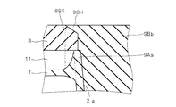
更に、半導体装置101によれば従来の半導体装置101Pよりも高速動作が可能である。かかる点を図20及び図21を参照しつつ説明する。図20及び図21は活性領域端付近ないしは溝2付近におけるN型のソース・ドレイン層(又はN+型層)とP型のチャネル不純物層との濃度分布を説明するための模式図であり、図20が半導体装置101に関するものであり、図21が従来の半導体装置101Pに関するものである。
【0078】
上述のように半導体装置101ではチャネル不純物層10の第1部分10Aが第2部分10B(及び従来のチャネル不純物層10P)よりも基板1の主面1Sの側に形成されており、第1部分10Aはソース・ドレイン層6(詳細にはN+型層6B)内に設けられている。より具体的には、図20に示すように、第1部分10A及びソース・ドレイン層6の不純物濃度分布の両ピークが、ソース・ドレイン層6と基板1との接合面(両層の分布曲線の交差点で与えられる)に対して同じ側に設定されている。このため、図20に示すように、活性領域端ではチャネル不純物層10の第1部分10Aがソース・ドレイン層6と大きく重なっている。換言すれば、ソース・ドレイン層6及び第1部分10Aの双方の高濃度領域ないしはピーク濃度領域が重なっている。これに対して、図21に示すように、形成深さの違いに起因して、従来のチャネル不純物層10Pはソース・ドレイン層6Pとの重なりが小さい。
【0079】
このとき、互いに逆の導電型の不純物はドーピング作用を相殺することに鑑みれば、図20に示す半導体装置101では、上記接合面の両側の不純物濃度は、図21に示す従来の半導体装置101Pのそれらよりも低い。このため、活性領域端では、半導体装置101の方が上記接合面での空乏層が基板1の深さ方向に広がりやすく、接合容量がより小さい。従って、活性領域全体についても半導体装置101の方が接合容量が小さく、その結果、動作をより高速化することができる。なお、接合容量の低減による高速化はチャネル不純物層10の第1部分10Aの一部がソース・ドレイン層6内に設けられていることによって得られ、基板1内での第1部分10Aの形成位置に依らない。
【0080】
<実施の形態1の変形例1>
なお、基板1,酸化膜7及び半導体膜11等がシリコンを含む場合を説明したが、これらがシリコン以外の他の半導体材料を含む場合であって上述の説明はあてはまる。
【0081】
また、上述の説明では半導体装置101がNMOSFETの場合を述べたが、基板1及び各層(又は各膜)の導電型を逆転させることによって、半導体装置101としてPチャネル型のMOSFET(PMOSFET)を提供することができる。また、NMOSFET及びPMOSFETを組み合わせることにより、半導体装置101としてCMOSFETを提供することも可能である。
【0082】
<実施の形態1の変形例2>
なお、ゲート絶縁膜4がシリコン酸化膜以外の場合であっても、即ち半導体装置101が一般的なMIS(metal-insulator-semiconductor)構造のFETを備える場合であっても、上述の説明は妥当である。
【0083】
また、ゲート電極5を、金属膜とポリシリコン膜との組み合わせ等の他の積層構造としても構わないし、又、シリサイド化したポリシリコン膜で形成しても良いし、又、金属膜のみで形成しても良い。
【0084】
<実施の形態2>
次に、実施の形態2に係る半導体装置102として、既述の半導体装置101を応用して得られるDRAM(dynamic random access memory)を説明する。図22に半導体装置102の(縦)断面図を示す。なお、以下の説明では、既述の要素と同等の要素には同一の符号を付してその説明を援用するに留める。
【0085】
図22に示すように、半導体装置102は溝2が形成された基板1を備え、溝2内に溝型素子分離を成すシリコン酸化膜9が埋め込まれている。なお、図22では詳細な図示化を省略するが、シリコン酸化膜9はシリコン酸化膜9A,9B(図2参照)から成る。
【0086】
そして、活性領域AR1(図1参照)内に2つのMOSFETが形成されている。詳細には、基板1の主面1S上に、所定の距離だけ離れて2つのゲート絶縁膜4が形成されており、それぞれのゲート絶縁膜4上にゲート電極5及びサイドウォール酸化膜41が形成されている。なお、ゲート電極5は例えば既述のポリシリコン膜5A及びタングステンシリサイド膜5B(図2参照)から成る。なお、図22中にはシリコン酸化膜9上にもゲート絶縁膜4,ゲート電極5及びサイドウォール酸化膜41が形成されているが、これらの構成要素(以下まとめて「ゲート要素4,5,41」とも呼ぶ)は、図22中には図示しない他の活性領域内に形成され、且つ、紙面に垂直な方向に延長形成されたものである。
【0087】
更に、基板1の主面1S内にソース・ドレイン層(ないしは第2及び第3不純物層)61,62が形成されている。各ソース・ドレイン層61,62は既述のソース・ドレイン層6(図2参照)に相当する。図22では詳細な図示化を省略するが、各ソース・ドレイン層61,62はN-型層6A及びN+型層6Bから成る。なお、ソース・ドレイン層62は上記2つのMOSFETに渡って形成されている。即ち、ソース・ドレイン層62は各MOSFETの各一方のソース・ドレイン層6が主面1S内で一体化した形態にあたる。
【0088】
更に、既述の半導体装置101と同様に、活性領域AR1(図1参照)内には基板1の主面1Sの全体に対面してチャネル不純物層10が形成されている。即ち、チャネル不純物層10の第1部分10Aは基板1内において溝2の側面2S(図2等参照)に接し、当該側面2Sに沿って形成されており、又、溝2の開口端付近ないしは主面1S付近に形成されている。しかも、第1部分10AはN+型層6B内に、即ちソース・ドレイン層6内に設けられている。チャネル不純物層10の第2部分10Bは第1部分10Aよりも深い位置に形成されている。
【0089】
以上の構造は実施の形態1で説明した製造方法により形成可能である。
【0090】
更に、ゲート要素4,5,41を覆って基板1の主面1S上に層間絶縁膜50Aが形成されており、かかる層間絶縁膜50Aの表面50ASからソース・ドレイン層62へ至る接続孔13が形成されている。層間絶縁膜50Aの表面50AS上には、接続孔13を介してソース・ドレイン層62に接続されたビット線14が形成されている。
【0091】
また、ビット線14を覆って層間絶縁膜50Aの表面50AS上に層間絶縁膜50Bが形成されており、かかる層間絶縁膜50Bの表面50BSからソース・ドレイン層61へ至る接続孔15が形成されている。層間絶縁膜50Bの表面50BS上には、接続孔15を介してソース・ドレイン層61に接続されたストレージノード16が形成されている。
【0092】
そして、ストレージノード16及び層間絶縁膜50Bの表面50BSを覆って、又、層間絶縁膜50Bの表面50BS上の凹凸に沿ってキャパシタ絶縁膜17が形成されている。更に、キャパシタ絶縁膜17上に当該キャパシタ絶縁膜17に沿ってセルプレート電極18が形成されている。
【0093】
セルプレート電極18を全面的に被覆して層間絶縁膜50Cが形成されており、層間絶縁膜50Cの表面50CS上に複数の配線19が形成されている。かかる配線層19は図22中に図示されない部分においてゲート電極5等と接続されている。
【0094】
半導体装置102によれば、半導体装置101と同様の効果を得ることができる。このとき、MOSFETのリーク電流の低減により、ストレージノード16に(即ちDRAMのキャパシタ部に)蓄積された電荷の損失を抑制することができる。
【0095】
【発明の効果】
請求項1に係る発明によれば、第2不純物層の内で第1不純物層の第1部分の一部が配置されている部分では、第2不純物層の不純物濃度を下げることができる。このため、かかる付近では第2不純物層と基板との接合面に形成される空乏層が広がりやすく、接合容量を小さくすることができる。これにより、接合面全体についても接合容量が小さくなるので、かかる接合容量が大きいが故に遅い動作速度を改善することができる。
【0096】
また、請求項1に係る発明によれば、第1不純物層の第1部分は溝の側面に沿って設けられている。溝内の誘電体上に配置された配線等からの電界は溝の側面から基板のポテンシャルに影響を及ぼす点に鑑みれば、第1部分によって溝付近での特性を補償することができる。これにより、半導体装置の上記電界に起因した動作不具合を低減することができる。
【0097】
また、請求項1に係る発明によれば、第1不純物層の第1部分は溝の開口端付近に設けられている。ところで、上述の誘電体上の配線からの電界は当該配線等に近いほど、即ち溝の開口端に近いほどより強い。このとき、第1不純物層の第1部分は上述の電界がより強い部分に設けられているので、上述の電界に起因した動作不具合をより確実に低減することができる。
【0098】
また、請求項1に係る発明によれば、第2不純物層及び(第2不純物層と同等の)第3不純物層が電界効果トランジスタのソース・ドレイン層を成すので、電界効果トランジスタの動作を、従って当該半導体装置の動作を高速化することができる。
【0099】
請求項2に係る発明によれば、電界効果トランジスタにおいてハンプや逆ナローチャネル効果を抑制してリーク電流を低減することができる。その結果、電界効果トランジスタを、更には半導体装置を所望の(設計の)特性で動作させることができる。また、半導体装置が当該電界効果トランジスタを含むDRAM(dynamic random access memory)の場合、上述のリーク電流の低減によって、DRAMのキャパシタ部に蓄積された電荷の損失を抑制することができる。
【図面の簡単な説明】
【図1】 実施の形態1に係る半導体装置の模式的な平面図である。
【図2】 実施の形態1に係る半導体装置の断面図である。
【図3】 実施の形態1に係る半導体装置の一部の断面図である。
【図4】 実施の形態1に係る半導体装置の断面図である。
【図5】 実施の形態1に係る半導体装置の断面図である。
【図6】 実施の形態1に係る半導体装置の一部の断面図である。
【図7】実施の形態1に係る半導体装置の断面図である。
【図8】 実施の形態1に係る半導体装置の製造方法を説明するための断面図である。
【図9】 実施の形態1に係る半導体装置の製造方法を説明するための断面図である。
【図10】 実施の形態1に係る半導体装置の製造方法を説明するための断面図である。
【図11】 実施の形態1に係る半導体装置の製造方法を説明するための断面図である。
【図12】 実施の形態1に係る半導体装置の製造方法を説明するための断面図である。
【図13】 実施の形態1に係る半導体装置の製造方法を説明するための断面図である。
【図14】 実施の形態1に係る半導体装置の製造方法を説明するための断面図である。
【図15】 実施の形態1に係る半導体装置の製造方法を説明するための断面図である。
【図16】 実施の形態1に係る半導体装置の製造方法を説明するための断面図である。
【図17】 実施の形態1に係る半導体装置の製造方法を説明するための模式図である。
【図18】 実施の形態1に係る半導体装置の製造方法を説明するための断面図である。
【図19】 実施の形態1に係る半導体装置の製造方法を説明するための断面図である。
【図20】 実施の形態1に係る半導体装置における不純物濃度分布を説明するための模式図である。
【図21】 従来の半導体装置における不純物濃度分布を説明するための模式図である。
【図22】 実施の形態2に係る半導体装置の断面図である。
【図23】 従来の半導体装置の模式的な平面図である。
【図24】 従来の半導体装置の断面図である。
【図25】 従来の半導体装置の断面図である。
【図26】 従来の半導体装置の一部の断面図である。
【図27】 従来の半導体装置の製造方法を説明するための断面図である。
【図28】 従来の半導体装置の製造方法を説明するための断面図である。
【図29】 従来の半導体装置の製造方法を説明するための断面図である。
【図30】 従来の半導体装置の製造方法を説明するための断面図である。
【図31】 従来の半導体装置の製造方法を説明するための断面図である。
【図32】 従来の半導体装置の動作特性図である。
【符号の説明】
1 基板、1S 主面、2,2a 溝、2S 側面、4 ゲート絶縁膜、5 ゲート電極、6,61,62 ソース・ドレイン層(第2又は第3不純物層)、6A N-型層、6B N+型層、7 シリコン酸化膜(酸化膜),7A 厚い部分,7B 薄い部分、9 シリコン酸化膜(誘電体)、9A,9Aa,9B,9Ba,9Bb シリコン酸化膜、10 チャネル不純物層(第1不純物層)、10A 第1部分、10B 第2部分、11 シリコン膜(半導体膜)、11S 表面、101,102 半導体装置、AR1 活性領域、AR2 素子分離領域。[0001]
BACKGROUND OF THE INVENTION
The present invention relates to a semiconductor device having a trench type element isolation structure and a method for manufacturing the same.
[0002]
[Prior art]
In a semiconductor integrated circuit, it is necessary to eliminate electrical interference between elements in order to control individual elements completely independently during operation. For this reason, an element isolation structure having an element isolation region is employed in a semiconductor integrated circuit. As one of such element isolation structures, the trench isolation method is widely known, and many improvements have been proposed.
[0003]
The trench isolation method is a method of electrically insulating elements from each other by forming a groove (trench) from the surface of the substrate toward the inside and filling the inside with a dielectric. This method hardly generates bird's beaks seen in the element isolation structure by the LOCOS method. For this reason, the trench isolation method is a preferable method for promoting the miniaturization of the semiconductor integrated circuit because it requires a smaller area on the substrate surface for formation than the element isolation structure by the LOCOS method. Therefore, it can be said that the trench isolation method is an element isolation method indispensable in a semiconductor integrated circuit that will be further miniaturized in the future.
[0004]
FIG. 23 shows a schematic plan view (top view) of a
[0005]
As shown in FIGS. 23 to 26, the
[0006]
A silicon oxide film 9AP is formed on the inner surface 2SP of the
[0007]
In the
[0008]
An N-channel field effect transistor (NMOSFET) is formed in the active region AR1P of the
[0009]
Two source /
[0010]
Further, a
[0011]
Next, a method for manufacturing the
[0012]
First, a
[0013]
Next, using a photoengraving technique, a resist (not shown) is formed on the
[0014]
Next, the silicon oxide film 9BaP is polished by chemical mechanical polishing (CMP) using the
[0015]
Then, the
[0016]
Next, a silicon oxide film is formed again by thermally oxidizing the main surface 1SP of the
[0017]
Thereafter, a silicon oxide film, a polysilicon film, and a tungsten silicide film are sequentially formed, and these are patterned to form a
[0018]
[Problems to be solved by the invention]
As described above, the
[0019]
As shown in FIG. 26, since the depression 9RP is formed lower than the main surface 1SP of the
[0020]
Such electric field concentration lowers the potential at the end of the active region, so that the threshold voltage at the end of the active region of the MOSFET is lower than that at the channel region (the central portion thereof). That is, a parasitic MOSFET (or parasitic element) having a threshold voltage lower than a desired (or designed) voltage is formed at the end of the active region. For this reason, at the time of operation, the parasitic MOSFET is first turned on, and then the parts other than the parasitic MOSFET are turned on. As a result, the drain current of the MOSFET starts to flow at a voltage lower than the desired threshold voltage, as indicated by a characteristic line β in FIG. 32, which is a characteristic diagram of the MOSFET. That is, a hump is observed in the characteristic diagram.
[0021]
Further, when the channel width is reduced as the device size is reduced, the presence of the parasitic MOSFET described above generates an inverse narrow channel effect in which the threshold voltage is lowered as the channel width is reduced. That is, in the MOSFET, current starts to flow at a voltage lower than a desired threshold voltage due to the reverse narrow channel effect.
[0022]
Even when there is no depression 9RP, the electric field from various wirings or the like formed in the element isolation region AR2P or on the
[0023]
As described above, the hump and the reverse narrow channel effect caused by the parasitic MOSFET cause an increase in the off-current or leakage current of the MOSFET, resulting in a problem that the yield of the
[0024]
It should be noted that such a dip is not formed in LOCOS due to a difference in formation method of element isolation, but as described above, a trench type element isolation structure is indispensable for promoting further miniaturization of a semiconductor device. It is.
[0025]
The present invention has been made in view of the above point, and mainly provides a semiconductor device capable of suppressing the formation of a parasitic element at the end of an active region and operating with desired characteristics, and a method of manufacturing the same. Objective.
[0026]
[Means for Solving the Problems]
Contract The semiconductor device according to
[0030]
[0035]
DETAILED DESCRIPTION OF THE INVENTION
<
FIG. 1 shows a schematic plan view (top view) of a
[0036]
As shown in FIGS. 1 to 7, the
[0037]
However, the element isolation region AR2 is not only a planar region on the
[0038]
The distance from the
[0039]
As shown in FIGS. 2 to 7, a
[0040]
The
[0041]
Specifically, the
[0042]
A
[0043]
Further, N-type source / drain layers (or second and third impurity layers) 6 having a conductivity type opposite to that of the
[0044]
More specifically, both source / drain layers 6 are formed of N-type N + Mold layer 6B and N + N having a lower impurity concentration than the mold layer 6B - It consists of a
[0045]
Further, a channel impurity layer (or first impurity layer) 10 for controlling the threshold voltage of the MOSFET is formed in the active region AR1. The
[0046]
Specifically, the
[0047]
On the other hand, the
[0048]
Here, a case where the threshold voltage of the MOSFET included in the
[0049]
At this time, in the
[0050]
Although illustration is omitted, a channel cut impurity layer is formed near the bottom 2B of the
[0051]
Next, a method for manufacturing the
[0052]
First, the
[0053]
Next, using a photoengraving technique, a resist (not shown) is formed on the exposed surface of the
[0054]
Next, the exposed surface of the substrate 1 (corresponding to the inner surface of the
[0055]
At this time, as shown in FIG. 11, the end portion along the
[0056]
Thereafter, as shown in FIG. 12, a silicon oxide film 9Ba is deposited by HDP (high density plasma) -CVD (chemical vapor deposition) so as to cover the entire
[0057]
In place of the silicon oxide film 9Ba, for example, a silicon oxynitride film, a PSG (phospho-silicate glass) film, a BPSG (boro-phosphosilicate glass) film, or an FSG (flourine doped silicon glass) film may be used. Further, the silicon oxide film 9Ba may be formed by a film forming method other than the HDP-CVD method. In addition, according to the film forming method in which etching (or sputtering) and film formation are performed simultaneously as in the above-described HDP-CVD method, the silicon oxide film 9Ba is filled in the
[0058]
Next, as shown in FIG. 13, a part of the silicon oxide film 9Ba shown in FIG. 12 is removed by CMP (chemical mechanical polishing) using the
[0059]
Thereafter, the
[0060]
Next, boron ions are implanted through the exposed
[0061]
Further, boron ions are implanted into the
[0062]
Next, the
[0063]
Thereafter, the exposed
[0064]
Next, phosphorus ions are implanted at about 20 keV to 50 keV by ion implantation. Subsequently, a sidewall oxide film 41 (see FIG. 2) is formed on the side surface of the
[0065]
According to the
[0066]
As described above, since the thermal oxidation method or the like is used to form the silicon oxide film 9Aa (or 9A), a thick portion 7A (see FIG. 11) can be formed in the
[0067]
By the way, even in the absence of the depression 9RP, the electric field from the wiring (including the gate electrode 5) formed in the element isolation region AR2 or on the
[0068]
In other words, in the
[0069]
In particular, in the
[0070]
As described above, when forming the
[0071]
In addition, when the
[0072]
In the above manufacturing method, RTA is performed after ion implantation for forming the
[0073]
In the manufacturing method described above, as shown in FIGS. 14 and 15, the
[0074]
Furthermore, according to the wet etching, the
[0075]
That is, since the above-described HDP-CVD method is a film forming method in which etching and film formation are performed simultaneously, when the silicon oxide film 9Ba is formed by the HDP-CVD method, the edge portion of the
[0076]
Thus, according to the above-described manufacturing method, the
[0077]
Furthermore, the
[0078]
As described above, in the
[0079]
At this time, in view of the fact that impurities of opposite conductivity types cancel the doping effect, in the
[0080]
<
Note that the case where the
[0081]
In the above description, the
[0082]
<
The above description is valid even when the
[0083]
Further, the
[0084]
<
Next, a DRAM (dynamic random access memory) obtained by applying the above-described
[0085]
As shown in FIG. 22, the
[0086]
Two MOSFETs are formed in the active region AR1 (see FIG. 1). Specifically, two
[0087]
Further, source / drain layers (or second and third impurity layers) 61 and 62 are formed in the
[0088]
Further, similarly to the
[0089]
The above structure can be formed by the manufacturing method described in
[0090]
Further, an
[0091]
An interlayer insulating film 50B is formed on the surface 50AS of the
[0092]
Then, the
[0093]
An interlayer insulating film 50C is formed covering the entire surface of the
[0094]
According to the
[0095]
【The invention's effect】
Contract According to the first aspect of the invention, the impurity concentration of the second impurity layer can be lowered in a portion of the second impurity layer where a part of the first portion of the first impurity layer is disposed. For this reason, a depletion layer formed on the junction surface between the second impurity layer and the substrate easily spreads in this vicinity, and the junction capacitance can be reduced. As a result, the junction capacity of the entire junction surface is also reduced, so that the slow operation speed can be improved because the junction capacity is large.
[0096]
In addition,
[0097]
In addition,
[0098]
In addition,
[0099]
[Brief description of the drawings]
FIG. 1 is a schematic plan view of a semiconductor device according to a first embodiment.
FIG. 2 is a cross-sectional view of the semiconductor device according to the first embodiment.
FIG. 3 is a partial cross-sectional view of the semiconductor device according to the first embodiment.
4 is a cross-sectional view of the semiconductor device according to the first embodiment. FIG.
FIG. 5 is a cross-sectional view of the semiconductor device according to the first embodiment.
FIG. 6 is a partial cross-sectional view of the semiconductor device according to the first embodiment.
FIG. 7 is a sectional view of the semiconductor device according to the first embodiment.
8 is a cross-sectional view for illustrating the method for manufacturing the semiconductor device according to the first embodiment. FIG.
FIG. 9 is a cross-sectional view for illustrating the method for manufacturing the semiconductor device according to the first embodiment.
10 is a cross-sectional view for illustrating the method for manufacturing the semiconductor device according to the first embodiment. FIG.
11 is a cross-sectional view for illustrating the method for manufacturing the semiconductor device according to the first embodiment; FIG.
12 is a cross-sectional view for illustrating the method for manufacturing the semiconductor device according to the first embodiment; FIG.
13 is a cross-sectional view for illustrating the method for manufacturing the semiconductor device according to the first embodiment. FIG.
14 is a cross-sectional view for illustrating the method of manufacturing the semiconductor device according to the first embodiment. FIG.
15 is a cross-sectional view for illustrating the method for manufacturing the semiconductor device according to the first embodiment. FIG.
FIG. 16 is a cross-sectional view for illustrating the method for manufacturing the semiconductor device according to the first embodiment.
17 is a schematic view for illustrating the method for manufacturing the semiconductor device according to the first embodiment. FIG.
FIG. 18 is a cross-sectional view for illustrating the method for manufacturing the semiconductor device according to the first embodiment.
FIG. 19 is a cross-sectional view for illustrating the method for manufacturing the semiconductor device according to the first embodiment.
20 is a schematic diagram for explaining an impurity concentration distribution in the semiconductor device according to the first embodiment; FIG.
FIG. 21 is a schematic diagram for explaining an impurity concentration distribution in a conventional semiconductor device.
FIG. 22 is a cross-sectional view of the semiconductor device according to the second embodiment.
FIG. 23 is a schematic plan view of a conventional semiconductor device.
FIG. 24 is a cross-sectional view of a conventional semiconductor device.
FIG. 25 is a cross-sectional view of a conventional semiconductor device.
FIG. 26 is a partial cross-sectional view of a conventional semiconductor device.
FIG. 27 is a cross-sectional view for illustrating the conventional method for manufacturing the semiconductor device.
FIG. 28 is a cross-sectional view for illustrating the conventional method for manufacturing the semiconductor device.
FIG. 29 is a cross-sectional view for illustrating the conventional method for manufacturing the semiconductor device.
FIG. 30 is a cross-sectional view for illustrating the conventional method for manufacturing the semiconductor device.
FIG. 31 is a cross-sectional view for illustrating the conventional method for manufacturing the semiconductor device.
FIG. 32 is an operational characteristic diagram of a conventional semiconductor device.
[Explanation of symbols]
1 substrate, 1S main surface, 2, 2a groove, 2S side surface, 4 gate insulating film, 5 gate electrode, 6, 61, 62 source / drain layer (second or third impurity layer), 6A N - Mold layer, 6B N + Type layer, 7 silicon oxide film (oxide film), 7A thick part, 7B thin part, 9 silicon oxide film (dielectric), 9A, 9Aa, 9B, 9Ba, 9Bb silicon oxide film, 10 channel impurity layer (first impurity) Layer), 10A first portion, 10B second portion, 11 silicon film (semiconductor film), 11S surface, 101, 102 semiconductor device, AR1 active region, AR2 element isolation region.
Claims (2)
前記基板の前記主面から前記基板の内部へ向けて形成された溝と、
前記溝内に形成された、溝型素子分離を成す誘電体と、
前記基板の前記所定の導電型と同じ導電型及び前記基板の前記所定の不純物濃度よりも高い不純物濃度を有し、前記基板の前記主面に対面して前記基板内に延在する第1不純物層と、
前記基板の前記所定の導電型とは反対の導電型を有し、前記基板の前記主面内の一部に形成された第2不純物層とを備え、
前記第1不純物層は、
第1部分と、
前記第1部分に連続し、前記基板の前記主面から前記第1部分よりも深くに延在する第2部分とを含み、
前記第1不純物層の前記第1部分の一部が前記第2不純物層内に形成されており、
前記第1不純物層の前記第1部分は前記溝の側面に沿って設けられており、
前記第1不純物層の前記第1部分は前記基板内において前記溝の開口端付近に設けられており、
前記第2不純物層と同じ導電型を有し、前記第2不純物層に接することなく前記基板の前記主面内の他の一部に形成された第3不純物層を更に備え、
前記第1不純物層の前記第1部分の内で前記一部とは異なる他の一部が前記第3不純物層内に形成されており、
前記第2不純物層及び前記第3不純物層をそれぞれソース・ドレイン層として含む電界効果トランジスタを更に備え、
前記第1不純物層の不純物濃度ピーク位置は、前記ソース・ドレイン層の不純物濃度ピーク位置と、前記ソース・ドレイン層と前記基板との接合面に対して同じ側にあることを特徴とする、
半導体装置。A substrate having a main surface and including a semiconductor material of a predetermined conductivity type having a predetermined impurity concentration;
A groove formed from the main surface of the substrate toward the inside of the substrate;
A dielectric formed in the trench to form trench-type element isolation;
A first impurity having the same conductivity type as the predetermined conductivity type of the substrate and an impurity concentration higher than the predetermined impurity concentration of the substrate and extending into the substrate facing the main surface of the substrate Layers,
A second impurity layer having a conductivity type opposite to the predetermined conductivity type of the substrate, and formed on a part of the main surface of the substrate;
The first impurity layer includes
A first part;
A second portion that is continuous with the first portion and extends deeper than the first portion from the main surface of the substrate;
A portion of the first portion of the first impurity layer is formed in the second impurity layer ;
The first portion of the first impurity layer is provided along a side surface of the groove;
The first portion of the first impurity layer is provided near the opening end of the groove in the substrate;
A third impurity layer having the same conductivity type as the second impurity layer and formed on another part of the main surface of the substrate without being in contact with the second impurity layer;
Another part of the first impurity layer that is different from the part of the first part is formed in the third impurity layer;
A field effect transistor including the second impurity layer and the third impurity layer as source / drain layers, respectively.
The impurity concentration peak position of the first impurity layer is on the same side as the impurity concentration peak position of the source / drain layer and the junction surface between the source / drain layer and the substrate ,
Semiconductor device.
前記電界効果トランジスタは、
前記基板の前記主面上に形成されたゲート絶縁膜と、
前記ゲート絶縁膜上及び前記誘電体上に延在するゲート電極を更に含むことを特徴とする、
半導体装置。The semiconductor device according to claim 1,
The field effect transistor is
A gate insulating film formed on the main surface of the substrate;
Further comprising a gate electrode extending on the gate insulating film and the dielectric ,
Semiconductor device.
Priority Applications (5)
| Application Number | Priority Date | Filing Date | Title |
|---|---|---|---|
| JP2000304372A JP4832629B2 (en) | 2000-10-04 | 2000-10-04 | Semiconductor device |
| US09/805,923 US6541825B2 (en) | 2000-10-04 | 2001-03-15 | Semiconductor device including impurity layer having continuous portions formed at different depths and method of manufacturing the same |
| TW090113457A TW490855B (en) | 2000-10-04 | 2001-06-04 | Semiconductor device and method of manufacturing the same |
| KR10-2001-0032296A KR100388585B1 (en) | 2000-10-04 | 2001-06-09 | Semiconductor device and method of manufacturing the same |
| US10/352,097 US6841440B2 (en) | 2000-10-04 | 2003-01-28 | Semiconductor device including impurity layer having continuous portions formed at different depths and method of manufacturing the same |
Applications Claiming Priority (1)
| Application Number | Priority Date | Filing Date | Title |
|---|---|---|---|
| JP2000304372A JP4832629B2 (en) | 2000-10-04 | 2000-10-04 | Semiconductor device |
Publications (3)
| Publication Number | Publication Date |
|---|---|
| JP2002110976A JP2002110976A (en) | 2002-04-12 |
| JP2002110976A5 JP2002110976A5 (en) | 2007-11-01 |
| JP4832629B2 true JP4832629B2 (en) | 2011-12-07 |
Family
ID=18785428
Family Applications (1)
| Application Number | Title | Priority Date | Filing Date |
|---|---|---|---|
| JP2000304372A Expired - Fee Related JP4832629B2 (en) | 2000-10-04 | 2000-10-04 | Semiconductor device |
Country Status (4)
| Country | Link |
|---|---|
| US (2) | US6541825B2 (en) |
| JP (1) | JP4832629B2 (en) |
| KR (1) | KR100388585B1 (en) |
| TW (1) | TW490855B (en) |
Families Citing this family (18)
| Publication number | Priority date | Publication date | Assignee | Title |
|---|---|---|---|---|
| JP4832629B2 (en) * | 2000-10-04 | 2011-12-07 | ルネサスエレクトロニクス株式会社 | Semiconductor device |
| US7248559B2 (en) | 2001-10-17 | 2007-07-24 | Nortel Networks Limited | Scattered pilot pattern and channel estimation method for MIMO-OFDM systems |
| DE10311312B4 (en) * | 2003-03-14 | 2007-08-16 | Infineon Technologies Ag | An insulator structure and method for producing insulator structures in a semiconductor substrate |
| JP4578785B2 (en) * | 2003-05-21 | 2010-11-10 | ルネサスエレクトロニクス株式会社 | Manufacturing method of semiconductor device |
| JP2005277024A (en) * | 2004-03-24 | 2005-10-06 | Oki Electric Ind Co Ltd | Semiconductor device and its manufacturing method |
| US7129559B2 (en) * | 2004-04-09 | 2006-10-31 | Taiwan Semiconductor Manufacturing Company, Ltd. | High voltage semiconductor device utilizing a deep trench structure |
| US20070235783A9 (en) * | 2005-07-19 | 2007-10-11 | Micron Technology, Inc. | Semiconductor constructions, memory arrays, electronic systems, and methods of forming semiconductor constructions |
| US7772672B2 (en) | 2005-09-01 | 2010-08-10 | Micron Technology, Inc. | Semiconductor constructions |
| KR100713924B1 (en) * | 2005-12-23 | 2007-05-07 | 주식회사 하이닉스반도체 | Fin transistor and method for forming thereof |
| US7799694B2 (en) * | 2006-04-11 | 2010-09-21 | Micron Technology, Inc. | Methods of forming semiconductor constructions |
| US7670888B2 (en) * | 2007-04-11 | 2010-03-02 | Texas Instruments Incorporated | Low noise JFET |
| US7906390B2 (en) * | 2007-07-20 | 2011-03-15 | International Business Machines Corporation | Thin gate electrode CMOS devices and methods of fabricating same |
| US8811339B2 (en) * | 2008-07-07 | 2014-08-19 | Blackberry Limited | Handover schemes for wireless systems |
| JP5629450B2 (en) * | 2009-10-16 | 2014-11-19 | キヤノン株式会社 | Semiconductor device and method for forming semiconductor device |
| US20120015474A1 (en) * | 2010-07-19 | 2012-01-19 | Yung-Chun Wu | Method for fabricating silicon heterojunction solar cells |
| JP2014007310A (en) * | 2012-06-26 | 2014-01-16 | Sumitomo Electric Ind Ltd | Silicon carbide semiconductor device manufacturing method and silicon carbide semiconductor device |
| US11322357B2 (en) * | 2020-03-02 | 2022-05-03 | Globalfoundries U.S. Inc. | Buried damage layers for electrical isolation |
| CN113066726B (en) * | 2021-03-19 | 2021-11-16 | 弘大芯源(深圳)半导体有限公司 | Method for realizing field effect transistor |
Family Cites Families (15)
| Publication number | Priority date | Publication date | Assignee | Title |
|---|---|---|---|---|
| JPS6199376A (en) | 1984-10-19 | 1986-05-17 | Sharp Corp | Manufacture of semiconductor device |
| JP2955459B2 (en) * | 1993-12-20 | 1999-10-04 | 株式会社東芝 | Method for manufacturing semiconductor device |
| JPH1065153A (en) * | 1996-08-15 | 1998-03-06 | Fujitsu Ltd | Semiconductor device and its manufacture |
| JPH10189951A (en) | 1996-12-26 | 1998-07-21 | Sanyo Electric Co Ltd | Manufacture of semiconductor device |
| JP3519571B2 (en) | 1997-04-11 | 2004-04-19 | 株式会社ルネサステクノロジ | Method for manufacturing semiconductor device |
| JPH118387A (en) * | 1997-06-18 | 1999-01-12 | Mitsubishi Electric Corp | Semiconductor device and manufacture thereof |
| JPH1131742A (en) * | 1997-07-14 | 1999-02-02 | Mitsubishi Electric Corp | Manufacture of semiconductor device |
| JP3519579B2 (en) | 1997-09-09 | 2004-04-19 | 株式会社ルネサステクノロジ | Semiconductor device and manufacturing method thereof |
| US6025232A (en) * | 1997-11-12 | 2000-02-15 | Micron Technology, Inc. | Methods of forming field effect transistors and related field effect transistor constructions |
| JP2000082808A (en) * | 1998-09-04 | 2000-03-21 | Toshiba Corp | Semiconductor device and manufacture thereof |
| JP2000150882A (en) * | 1998-09-04 | 2000-05-30 | Toshiba Corp | Mis type semiconductor device and its manufacture |
| JP3415459B2 (en) * | 1998-12-07 | 2003-06-09 | 株式会社東芝 | Semiconductor device and manufacturing method thereof |
| US6287920B1 (en) * | 1999-09-07 | 2001-09-11 | Texas Instruments Incorporated | Method of making multiple threshold voltage integrated of circuit transistors |
| US6277710B1 (en) * | 1999-11-15 | 2001-08-21 | Chartered Semiconductor Manufacturing Ltd. | Method of forming shallow trench isolation |
| JP4832629B2 (en) * | 2000-10-04 | 2011-12-07 | ルネサスエレクトロニクス株式会社 | Semiconductor device |
-
2000
- 2000-10-04 JP JP2000304372A patent/JP4832629B2/en not_active Expired - Fee Related
-
2001
- 2001-03-15 US US09/805,923 patent/US6541825B2/en not_active Expired - Lifetime
- 2001-06-04 TW TW090113457A patent/TW490855B/en not_active IP Right Cessation
- 2001-06-09 KR KR10-2001-0032296A patent/KR100388585B1/en not_active IP Right Cessation
-
2003
- 2003-01-28 US US10/352,097 patent/US6841440B2/en not_active Expired - Lifetime
Also Published As
| Publication number | Publication date |
|---|---|
| US20020038901A1 (en) | 2002-04-04 |
| US6841440B2 (en) | 2005-01-11 |
| US20030143810A1 (en) | 2003-07-31 |
| TW490855B (en) | 2002-06-11 |
| US6541825B2 (en) | 2003-04-01 |
| JP2002110976A (en) | 2002-04-12 |
| KR100388585B1 (en) | 2003-06-25 |
| KR20020027161A (en) | 2002-04-13 |
Similar Documents
| Publication | Publication Date | Title |
|---|---|---|
| US6770535B2 (en) | Semiconductor integrated circuit device and process for manufacturing the same | |
| JP4832629B2 (en) | Semiconductor device | |
| JP5137310B2 (en) | Structure including trench capacitor array and method of forming the same (simplified buried plate structure and process for SOI chip) | |
| JP4776755B2 (en) | Semiconductor device and manufacturing method thereof | |
| JP4931267B2 (en) | Semiconductor device | |
| US7791163B2 (en) | Semiconductor device and its manufacturing method | |
| US20020003256A1 (en) | MOS semiconductor device and method of manufacturing the same | |
| US7348235B2 (en) | Semiconductor device and method of manufacturing the same | |
| JP2005517299A (en) | Capacitor-less one-transistor DRAM cell and fabrication method | |
| JPH11168190A (en) | Memory cell | |
| US6469347B1 (en) | Buried-channel semiconductor device, and manufacturing method thereof | |
| US20070120182A1 (en) | Transistor having recess gate structure and method for fabricating the same | |
| US7772634B2 (en) | Semiconductor device and manufacturing method thereof | |
| US20070187752A1 (en) | Memory cell with a vertical transistor and fabrication method thereof | |
| JPH11284146A (en) | Semiconductor storage device and its manufacture | |
| JPWO2003069675A1 (en) | Manufacturing method of semiconductor device | |
| US5933745A (en) | Method of making total dielectric semiconductor device isolation region | |
| US6917064B2 (en) | Trench capacitor and a method for manufacturing the same | |
| US20150295033A1 (en) | Apparatus and method for manufacturing same | |
| KR100642649B1 (en) | Semiconductor device applying well bias and method offabricating the same | |
| JPH11284137A (en) | Semiconductor storage device and its manufacture | |
| JPH11317506A (en) | Semiconductor device and its manufacturing method | |
| JP4989076B2 (en) | Manufacturing method of semiconductor device | |
| JP2004080000A (en) | Method of manufacturing semiconductor memory device | |
| JP2002141408A (en) | Semiconductor device and method of manufacturing the same |
Legal Events
| Date | Code | Title | Description |
|---|---|---|---|
| A521 | Request for written amendment filed |
Free format text: JAPANESE INTERMEDIATE CODE: A523 Effective date: 20070913 |
|
| A621 | Written request for application examination |
Free format text: JAPANESE INTERMEDIATE CODE: A621 Effective date: 20070913 |
|
| RD04 | Notification of resignation of power of attorney |
Free format text: JAPANESE INTERMEDIATE CODE: A7424 Effective date: 20070913 |
|
| A977 | Report on retrieval |
Free format text: JAPANESE INTERMEDIATE CODE: A971007 Effective date: 20090403 |
|
| A711 | Notification of change in applicant |
Free format text: JAPANESE INTERMEDIATE CODE: A712 Effective date: 20100524 |
|
| A131 | Notification of reasons for refusal |
Free format text: JAPANESE INTERMEDIATE CODE: A131 Effective date: 20110705 |
|
| A521 | Request for written amendment filed |
Free format text: JAPANESE INTERMEDIATE CODE: A523 Effective date: 20110830 |
|
| TRDD | Decision of grant or rejection written | ||
| A01 | Written decision to grant a patent or to grant a registration (utility model) |
Free format text: JAPANESE INTERMEDIATE CODE: A01 Effective date: 20110920 |
|
| A01 | Written decision to grant a patent or to grant a registration (utility model) |
Free format text: JAPANESE INTERMEDIATE CODE: A01 |
|
| A61 | First payment of annual fees (during grant procedure) |
Free format text: JAPANESE INTERMEDIATE CODE: A61 Effective date: 20110921 |
|
| R150 | Certificate of patent or registration of utility model |
Free format text: JAPANESE INTERMEDIATE CODE: R150 |
|
| FPAY | Renewal fee payment (event date is renewal date of database) |
Free format text: PAYMENT UNTIL: 20140930 Year of fee payment: 3 |
|
| S531 | Written request for registration of change of domicile |
Free format text: JAPANESE INTERMEDIATE CODE: R313531 |
|
| R350 | Written notification of registration of transfer |
Free format text: JAPANESE INTERMEDIATE CODE: R350 |
|
| LAPS | Cancellation because of no payment of annual fees |