JP4831446B2 - Micro valve device - Google Patents
Micro valve device Download PDFInfo
- Publication number
- JP4831446B2 JP4831446B2 JP2000569132A JP2000569132A JP4831446B2 JP 4831446 B2 JP4831446 B2 JP 4831446B2 JP 2000569132 A JP2000569132 A JP 2000569132A JP 2000569132 A JP2000569132 A JP 2000569132A JP 4831446 B2 JP4831446 B2 JP 4831446B2
- Authority
- JP
- Japan
- Prior art keywords
- layer
- displaceable member
- microvalve
- actuator
- patent document
- Prior art date
- Legal status (The legal status is an assumption and is not a legal conclusion. Google has not performed a legal analysis and makes no representation as to the accuracy of the status listed.)
- Expired - Lifetime
Links
Images


Classifications
-
- F—MECHANICAL ENGINEERING; LIGHTING; HEATING; WEAPONS; BLASTING
- F16—ENGINEERING ELEMENTS AND UNITS; GENERAL MEASURES FOR PRODUCING AND MAINTAINING EFFECTIVE FUNCTIONING OF MACHINES OR INSTALLATIONS; THERMAL INSULATION IN GENERAL
- F16K—VALVES; TAPS; COCKS; ACTUATING-FLOATS; DEVICES FOR VENTING OR AERATING
- F16K99/00—Subject matter not provided for in other groups of this subclass
- F16K99/0001—Microvalves
-
- B—PERFORMING OPERATIONS; TRANSPORTING
- B81—MICROSTRUCTURAL TECHNOLOGY
- B81B—MICROSTRUCTURAL DEVICES OR SYSTEMS, e.g. MICROMECHANICAL DEVICES
- B81B3/00—Devices comprising flexible or deformable elements, e.g. comprising elastic tongues or membranes
- B81B3/0018—Structures acting upon the moving or flexible element for transforming energy into mechanical movement or vice versa, i.e. actuators, sensors, generators
- B81B3/0024—Transducers for transforming thermal into mechanical energy or vice versa, e.g. thermal or bimorph actuators
-
- F—MECHANICAL ENGINEERING; LIGHTING; HEATING; WEAPONS; BLASTING
- F15—FLUID-PRESSURE ACTUATORS; HYDRAULICS OR PNEUMATICS IN GENERAL
- F15C—FLUID-CIRCUIT ELEMENTS PREDOMINANTLY USED FOR COMPUTING OR CONTROL PURPOSES
- F15C3/00—Circuit elements having moving parts
-
- F—MECHANICAL ENGINEERING; LIGHTING; HEATING; WEAPONS; BLASTING
- F15—FLUID-PRESSURE ACTUATORS; HYDRAULICS OR PNEUMATICS IN GENERAL
- F15C—FLUID-CIRCUIT ELEMENTS PREDOMINANTLY USED FOR COMPUTING OR CONTROL PURPOSES
- F15C4/00—Circuit elements characterised by their special functions
-
- F—MECHANICAL ENGINEERING; LIGHTING; HEATING; WEAPONS; BLASTING
- F15—FLUID-PRESSURE ACTUATORS; HYDRAULICS OR PNEUMATICS IN GENERAL
- F15C—FLUID-CIRCUIT ELEMENTS PREDOMINANTLY USED FOR COMPUTING OR CONTROL PURPOSES
- F15C5/00—Manufacture of fluid circuit elements; Manufacture of assemblages of such elements integrated circuits
-
- F—MECHANICAL ENGINEERING; LIGHTING; HEATING; WEAPONS; BLASTING
- F16—ENGINEERING ELEMENTS AND UNITS; GENERAL MEASURES FOR PRODUCING AND MAINTAINING EFFECTIVE FUNCTIONING OF MACHINES OR INSTALLATIONS; THERMAL INSULATION IN GENERAL
- F16K—VALVES; TAPS; COCKS; ACTUATING-FLOATS; DEVICES FOR VENTING OR AERATING
- F16K99/00—Subject matter not provided for in other groups of this subclass
- F16K99/0001—Microvalves
- F16K99/0003—Constructional types of microvalves; Details of the cutting-off member
- F16K99/0011—Gate valves or sliding valves
-
- F—MECHANICAL ENGINEERING; LIGHTING; HEATING; WEAPONS; BLASTING
- F16—ENGINEERING ELEMENTS AND UNITS; GENERAL MEASURES FOR PRODUCING AND MAINTAINING EFFECTIVE FUNCTIONING OF MACHINES OR INSTALLATIONS; THERMAL INSULATION IN GENERAL
- F16K—VALVES; TAPS; COCKS; ACTUATING-FLOATS; DEVICES FOR VENTING OR AERATING
- F16K99/00—Subject matter not provided for in other groups of this subclass
- F16K99/0001—Microvalves
- F16K99/0034—Operating means specially adapted for microvalves
- F16K99/0042—Electric operating means therefor
- F16K99/0044—Electric operating means therefor using thermo-electric means
-
- F—MECHANICAL ENGINEERING; LIGHTING; HEATING; WEAPONS; BLASTING
- F16—ENGINEERING ELEMENTS AND UNITS; GENERAL MEASURES FOR PRODUCING AND MAINTAINING EFFECTIVE FUNCTIONING OF MACHINES OR INSTALLATIONS; THERMAL INSULATION IN GENERAL
- F16K—VALVES; TAPS; COCKS; ACTUATING-FLOATS; DEVICES FOR VENTING OR AERATING
- F16K99/00—Subject matter not provided for in other groups of this subclass
- F16K2099/0073—Fabrication methods specifically adapted for microvalves
- F16K2099/0074—Fabrication methods specifically adapted for microvalves using photolithography, e.g. etching
-
- F—MECHANICAL ENGINEERING; LIGHTING; HEATING; WEAPONS; BLASTING
- F16—ENGINEERING ELEMENTS AND UNITS; GENERAL MEASURES FOR PRODUCING AND MAINTAINING EFFECTIVE FUNCTIONING OF MACHINES OR INSTALLATIONS; THERMAL INSULATION IN GENERAL
- F16K—VALVES; TAPS; COCKS; ACTUATING-FLOATS; DEVICES FOR VENTING OR AERATING
- F16K99/00—Subject matter not provided for in other groups of this subclass
- F16K2099/0073—Fabrication methods specifically adapted for microvalves
- F16K2099/008—Multi-layer fabrications
-
- F—MECHANICAL ENGINEERING; LIGHTING; HEATING; WEAPONS; BLASTING
- F16—ENGINEERING ELEMENTS AND UNITS; GENERAL MEASURES FOR PRODUCING AND MAINTAINING EFFECTIVE FUNCTIONING OF MACHINES OR INSTALLATIONS; THERMAL INSULATION IN GENERAL
- F16K—VALVES; TAPS; COCKS; ACTUATING-FLOATS; DEVICES FOR VENTING OR AERATING
- F16K99/00—Subject matter not provided for in other groups of this subclass
- F16K2099/0082—Microvalves adapted for a particular use
- F16K2099/0098—Refrigeration circuits, e.g. for cooling integrated circuits
-
- Y—GENERAL TAGGING OF NEW TECHNOLOGICAL DEVELOPMENTS; GENERAL TAGGING OF CROSS-SECTIONAL TECHNOLOGIES SPANNING OVER SEVERAL SECTIONS OF THE IPC; TECHNICAL SUBJECTS COVERED BY FORMER USPC CROSS-REFERENCE ART COLLECTIONS [XRACs] AND DIGESTS
- Y10—TECHNICAL SUBJECTS COVERED BY FORMER USPC
- Y10T—TECHNICAL SUBJECTS COVERED BY FORMER US CLASSIFICATION
- Y10T137/00—Fluid handling
- Y10T137/0318—Processes
- Y10T137/0396—Involving pressure control
Landscapes
- Engineering & Computer Science (AREA)
- General Engineering & Computer Science (AREA)
- Mechanical Engineering (AREA)
- Chemical & Material Sciences (AREA)
- Dispersion Chemistry (AREA)
- Computer Hardware Design (AREA)
- Microelectronics & Electronic Packaging (AREA)
- Theoretical Computer Science (AREA)
- Physics & Mathematics (AREA)
- Fluid Mechanics (AREA)
- Analytical Chemistry (AREA)
- Micromachines (AREA)
- Temperature-Responsive Valves (AREA)
- Diaphragms For Electromechanical Transducers (AREA)
- Electrically Driven Valve-Operating Means (AREA)
Abstract
Description
【0001】
(発明の背景)
(1.発明の分野)
本発明は、概して、半導体電子機械微小デバイス、より具体的には、高アスペクト比ジオメトリー、およびトランスデューサに関して変位可能な部材を有する微小デバイスに関する。
【0002】
(2.関連技術の説明)
流体バルブは、概して、流体ポート、アクチュエータ、および、アクチュエータに応答して流体ポートを開閉する可動のバルブ構造を備える。流体バルブには、多くのタイプがある。流体バルブの例には、バイメタリックマイクロバルブおよびカプセル化流体マイクロバルブのような、微細加工半導体材料から製造されるソレノイドバルブおよびマイクロバルブが含まれる。しかし、これらのバルブまたはマイクロバルブのタイプの各々について、多くの問題がある。
【0003】
ソレノイドバルブは、シリンダの形態のコイルを利用し、概して、電流がコイルを流れる場合に始動される磁界によって、シリンダの中に引き込まれ得るコアを有する。ソレノイドバルブは、典型的には、例えば従来のアンチロックブレーキシステムにおいて用いられる。しかし、ソレノイドバルブは、通常、比較的大きく、重量がある。さらに、ソレノイドバルブのような電磁バルブは、しばしば、比較的高い電流を必要とし、電圧供給のスパイキングを引き起こし得る。ソレノイドバルブは、また、ヒステリシスを表し得、そのことによって、電子入力に対する非線形性の応答を表し得る。さらに、ソレノイドバルブのような電磁バルブの動作は、そのようなバルブへの電流の送達と、得られる磁界および対応する力との間の比較的長いラグタイムに起因して、比較的遅くなり得る。また、ソレノイドバルブを部分的にのみ開けるか、または閉めるかすることは困難であり、従って、ソレノイドバルブは、典型的には、比例したバルブとしてよりむしろ、オン/オフバルブとして用いられる。
【0004】
例示的なバイメタリックマイクロバルブは、異なる熱膨張率を有する2つの材料から製造されるアクチュエータを利用する。熱膨張率の違いによって、アクチュエータを加熱または冷却する際にアクチュエータが曲がったり、まっすぐになったりし、そのことによって、フローオリフィスを開閉する。米国特許第5,058,856号には、第1および第2の基板を有するこのようなバイメタリックマイクロバルブが開示されている。第1の基板は、フローオリフィスおよびバルブシートを規定する。第2の基板は、フローオリフィスと並べられたバルブフェースを規定し、また、可動アクチュエータを規定する。可動アクチュエータは、シリコン層およびニッケル層のような、実質的に異なる熱膨張率を有する材料の第1および第2の層を含む。アクチュエータは、また、加熱要素を含み、選択的な加熱によって、熱膨張率の違いに起因してアクチュエータが曲げられるように、一方の端部で固定される。アクチュエータが曲がることによって、バルブフェースがバルブシートから外れるか、または、バルブシートに向いて、バルブを開閉し、そのことにより、オリフィスを流れる流体フローを制御する。
【0005】
しかし、このようなバイメタリックマイクロバルブに関する問題点の1つとして、温度の変化に応答してアクチュエータが始動するため、外気温の変化によって、意図しないマイクロバルブの始動が起こり得ることがある。さらに、加熱された要素、すなわち、アクチュエータは、流体フローと接触しているので、流体経路の中の流体に対して望ましくない加熱を行い、加熱器を冷却し、アクチュエータを変位し得る。さらに、アクチュエータの変位が、また、比較的小さく、概して、10ppm/℃のオーダーである。
【0006】
カプセル化流体マイクロバルブの一例が、米国特許第4,824,073号に開示されている。カプセル化流体マイクロバルブは、キャビティの1つ以上の壁を形成するフレキシブル薄膜またはダイヤフラムを変形させるように加熱する場合の密閉キャビティにおける一定量の流体または気体の膨張および昇圧の原理を利用する。カプセル化流体また気体が加熱される場合、ダイヤフラムが変形されて、ポートを開閉し、流体オリフィスを流れる流体フローが制御される。カプセル化流体また気体の加熱は、キャビティ内の抵抗加熱要素によって、電流が抵抗要素を流れ、流体または気体を加熱する熱を発生するように達成される。
【0007】
カプセル化流体マイクロバルブは、比較的大きい力を発生し得るので、例えば大量の流体フローを制御する、大量流体コントローラとして用いられ得る。さらに、カプセル化流体マイクロバルブは、また、比例して動作して、流体制御の比例する範囲を提供し得る。すなわち、バルブは、制御信号の大きさによって、バルブを流れる流体フローの割合を調整するように制御され得る。
【0008】
しかし、カプセル化流体マイクロバルブは、流体の加熱および冷却に必要な時間に起因して、比較的遅い応答時間を有する。さらに、カプセル化流体マイクロバルブの変形膜は、流体または気体流路と接触している。従って、膜の変形温度が流路の中の流体または気体の温度に影響を及ぼし得、流路の中の流体または気体の温度が変形膜の温度に影響を及ぼし得る。
【0009】
さらに、上記のバルブのいずれも、マイクロバルブを流れる流体フローの効果を最小化する、フロー−力および/または圧力−力の補償を提供しない。
【特許文献1】
日本特許公告昭49−039223号1974年12月
【特許文献2】
特許公告昭49−039224号1974年12月
【特許文献3】
日本特許公告昭49−048264号1974年10月
【特許文献4】
日本特許公告昭49−048265号1974年10月
【特許文献5】
日本特許公開平06ー56014号1994年3月
【特許文献6】
日本特許公開平06−286600号1994年10月
【特許文献7】
日本特許公告昭59−2175号1984年1月
【特許文献8】
日本特許公告昭59−2175号1984年1月
【特許文献9】
米国特許第3747628 号 1973年7月
【特許文献10】
米国特許第3860949 号 1975年1月
【特許文献11】
米国特許第4005454 号 1977年1月
【特許文献12】
米国特許第4019388 号 1977年4月
【特許文献13】
米国特許第4023725 号 1977年5月
【特許文献14】
米国特許第4152540 号 1979年5月
【特許文献15】
米国特許第4181249 号 1980年1月
【特許文献16】
米国特許第4298023 号 1981年11月
【特許文献17】
米国特許第4341816 号 1982年7月
【特許文献18】
米国特許第4434813 号 1984年3月
【特許文献19】
米国特許第4581624 号 1986年4月
【特許文献20】
米国特許第4628576 号 1986年12月
【特許文献21】
米国特許第4647013 号 1987年3月
【特許文献22】
米国特許第4661835 号 1987年4月
【特許文献23】
米国特許第4772935 号 1988年9月
【特許文献24】
米国特許第4821997 号 1989年4月
【特許文献25】
米国特許第4824073 号 1989年4月
【特許文献26】
米国特許第4826131 号 1989年5月
【特許文献27】
米国特許第4828184 号 1989年5月
【特許文献28】
米国特許第4869282 号 1989年9月
【特許文献29】
米国特許第4938742 号 1990年7月
【特許文献30】
米国特許第4943032 号 1990年7月
【特許文献31】
米国特許第4959581 号 1990年9月
【特許文献32】
米国特許第4966646 号 1990年10月
【特許文献33】
米国特許第5029805 号 1991年7月
【特許文献34】
米国特許第5037778 号 1991年8月
【特許文献35】
米国特許第5050838 号 1991年9月
【特許文献36】
米国特許第5054522 号 1991年10月
【特許文献37】
米国特許第5058856 号 1991年10月
【特許文献38】
米国特許第5061914 号 1991年10月
【特許文献39】
米国特許第5064165 号 1991年11月
【特許文献40】
米国特許第5065978 号 1991年11月
【特許文献41】
米国特許第5066533 号 1991年11月
【特許文献42】
米国特許第5069419 号 1991年12月
【特許文献43】
米国特許第5074629 号 1991年12月
【特許文献44】
米国特許第5082242 号 1992年1月
【特許文献45】
米国特許第5096643 号 1992年3月
【特許文献46】
米国特許第5116457 号 1992年5月
【特許文献47】
米国特許第5131729 号 1992年7月
【特許文献48】
米国特許第5133379 号 1992年7月
【特許文献49】
米国特許第5142781 号 1992年9月
【特許文献50】
米国特許第5161774 号 1992年11月
【特許文献51】
米国特許第5169472 号 1992年12月
【特許文献52】
米国特許第5176358 号 1993年1月
【特許文献53】
米国特許第5177579 号 1993年1月
【特許文献54】
米国特許第5178190 号 1993年1月
【特許文献55】
米国特許第5179499 号 1993年1月
【特許文献56】
米国特許第5180623 号 1993年1月
【特許文献57】
米国特許第5197517 号 1993年3月
【特許文献58】
米国特許第5209118 号 1993年5月
【特許文献59】
米国特許第5215244 号 1993年6月
【特許文献60】
米国特許第5216273 号 1993年6月
【特許文献61】
米国特許第5217283 号 1993年6月
【特許文献62】
米国特許第5238223 号 1993年8月
【特許文献63】
米国特許第5244537 号 1993年9月
【特許文献64】
米国特許第5267589 号 1993年12月
【特許文献65】
米国特許第5271431 号 1993年12月
【特許文献66】
米国特許第5271597 号 1993年12月
【特許文献67】
米国特許第5309943 号 1994年5月
【特許文献68】
米国特許第5325880 号 1994年7月
【特許文献69】
米国特許第5333831 号 1994年8月
【特許文献70】
米国特許第5336062 号 1994年8月
【特許文献71】
米国特許第5355712 号 1994年10月
【特許文献72】
米国特許第5368704 号 1994年11月
【特許文献73】
米国特許第5400824 号 1995年3月
【特許文献74】
米国特許第5417235 号 1995年5月
【特許文献75】
米国特許第5445185 号 1995年8月
【特許文献76】
米国特許第5553790 号 1996年9月
【特許文献77】
米国特許第5556703 号 1996年9月
【特許文献78】
米国特許第5577533 号 1996年11月
【特許文献79】
米国特許第5785295 号 1998年7月
【特許文献80】
米国特許第5810325 号 1998年9月
【特許文献81】
米国特許第5838351 号 1998年11月
【特許文献82】
米国特許第5848605 号 1998年12月
【特許文献83】
米国特許第5873385 号 1999年2月
【特許文献84】
米国特許第5909078 号 1999年6月
【特許文献85】
米国特許第5926955 号 1999年7月
【特許文献86】
米国特許第5941608 号 1999年8月
【特許文献87】
米国特許第6019437 号 2000年2月
【特許文献88】
米国特許第6105737 号 2000年8月
【特許文献89】
米国特許第6523560 号 2003年2月
【特許文献90】
ドイツ特許第2215526 号 1973年10月
【特許文献91】
ドイツ特許第2930779 号 1980年2月
【特許文献92】
ドイツ特許第4101575 号 1992年7月
【特許文献93】
ドイツ特許第4417251 号 1995年11月
【特許文献94】
ドイツ特許第4422942 号 1996年1月
【特許文献95】
欧州特許第0250948 号 1988年1月
【特許文献96】
欧州特許第0261972 号 1988年3月
【特許文献97】
英国特許第2238267 号 1991年5月
【特許文献98】
国際特許第9916096 号 1999年4月
【非特許文献1】
Qi, J. and Johnson, W. et al. (Apr. 6-9, 1999) "Flip Chip on Laminate Manufacturability," 1999 International Conference on High Density Packaging and MCMs. Proc. SPEI--Int. Soc. Opt. Eng. (USA), Denver, CO., pp. 345-352. .
【非特許文献2】
Search Report (Mar. 15, 2000) PCT/US 99/19971. .
【非特許文献3】
Williams, K. R. et al. (Jun. 7-10, 1999). "A Silicon Microvalve for the Proportional Control of Fluids," Transducers '99 Sendai, Japan., pp. 1804-1807. .
【非特許文献4】
Yunkin, V.A., et al. (1994). "Highly Anisotropic Selective Reactive Ion Etching of Deep Trenches in Silicon," Microelectronic Engineering 23:373-376. .
【非特許文献5】
Bartha, J.W., et al., (1995). "Low Temperature Etching of Si in High Density Plasma Using SF.sub.6 /O.sub.2," Microelectronic Engineering, 27:453-456. .
【非特許文献6】
Carpenter Technology Corporation Technical Data sheet for "Carpenter Low Expansion ;42", date Nov. 1980 <http://www.carpenter.idesinc.com/datasheet. asp?e=181&u=eVIEW=PRINTER> (visited on Mar. 28, 2002). .
【非特許文献7】
Delphi Automotive Systems product brochure (1997). Variable Bleed Solenoid (VBS) for Transmission, copyright 1997. .
【非特許文献8】
Delphi Automotive Systems product brochure (1998). On/Off Transmission Solenoids, copyright 1998. .
【非特許文献9】
Duffy, James E. (1994). "Automatic Transmission Fundamentals," Modern Automotive Technology, copyright 1994, p. 707. .
【非特許文献10】
Fung, C.D., et al. (Nov. 7-8, 1984). "Deep Etching of Silicon Using Plasma," Proceedings of the Workshop on Micromachining and Micropackaging of Transducers, pp. 159-164. .
【非特許文献11】
Houston, P. N. et al. (Jun. 1-4, 1999). "Low Cost Flip Chip Processing and Reliability of Fast-Flow, Snap-Cure Underfills," 1999 Electronic Components and Technology Conference. San Diego, CA, pp. 61-70. .
【非特許文献12】
Jonsmann, J. et al. (Jan. 17-21, 1999). "Compliant Electro-thermal Microactuator" Twelfth IEEE International Conference on Micro Electro Mechanical Systems Orlando, Florida, IEEE Technical Digest entitled IEEE Catalog No.: 99CH36291C pp. 588-593. .
【非特許文献13】
Klaasen, E.H. et al.(1995). "Silicon Fusion Bonding and Deep Reactive Ion Etching; A New Technology for Microstructures," Proc. Tranducers 95 Stockholm Sweden pp. 556-559. .
【非特許文献14】
Konarski, Mark M. (May 31 to Jun. 4, 1998). "Cure Parameter Effects on the Tg and CTE of Flip Encapsulants," 43rd International SAMPE Symposium and Exhibition. Materials and Process Affordability. Keys to the Future. Anaheim, CA, vol. 1 pp. 823-832. .
【非特許文献15】
Linder, C. et al. (Jun. 1991). "Deep Dry Etching Techniques as a new IC Compatible Tool for Silicon Micromachining," Proceedings, Transducers '91 pp. 524-527. .
【非特許文献16】
Madou, Marc (1997). "Scaling Laws, Actuators, and Power in Miniaturization," Chapter 9 In Fundamentals of Microfabrication CRC Press LLC: Boca Raton, FL., pp. 405-446. .
【非特許文献17】
Noworolski, J.M. et al., (1996) "Process for in plane-and out-of-plane single crystal-silicon thermal conductors" Sensors and Actuators 55(1):65-69. .
【非特許文献18】
Ohio State Univesity Chemistry Department brochure page on Marc J. Madou [online]. Ohio State University [retrieved on Dec. 31, 2000]. Retrieved from Internet: <URL: http://www.chemistry.ohio-state.edu/resource/pubs/brochure/madou.htm>. .
【非特許文献19】
Petersen, K.E. et al.(Jun. 1991). "Surface Micromachined Structures Fabricated with Silicon Fusion Bonding," Proceedings, Transducers '91 pp. 397-399. .
【非特許文献20】
Author Unknown. (Sep./Oct. 1999). "HiTecMetal Group Develops Niche Market for Brazed Laminated Assemblies," Fluid Power Journal 27. .
【非特許文献21】
Ayon, A.A. et al. (Jun. 1998). "Etching Characteristics and Profile Control in a Time-Multiplexed ICP Etcher," Proc. of Solid State Sensor and Actuator Workshop Hilton Head SC pp. 41-44. .
【非特許文献22】
Eaton Corporation. "Products: Powertrain," located at <http://www.autocontrols.eaton.com/powertrain_body.html> visited on Sep. 1, 1999. (2 pages)..
【0010】
従って、小さく、軽量で、費用効率が高く、製造方法が簡単で、且つ素早い反応時間を有するマイクロバルブが必要とされてきた。また、制御刺激入力への応答が線形であり、ヒステリシスがなく、マイクロバルブを流れる流体フローの効果を最小化する、フロー−力および/または圧力−力補償を有する、精密且つ比例する流体制御を提供するマイクロバルブが必要とされてきた。また、バルブの動作がバルブを流れる流体または気体を大幅に加熱することのないバルブが必要とされてきた。さらに、外気温から独立して機能するマイクロバルブが必要とされてきた。本発明は、これらの必要性を満たす。
【0011】
(発明の要旨)
本発明の1つの局面によると、半導体微小機械デバイスは、概して、第1のほぼ平面の層、および第2のほぼ平面の半導体層を含む。第1および第2の部材は、第2の層から垂れ下がり、各々が第2の層によって規定されるキャビティ内に浮遊する。第1の層は、また、キャビティの一部分を規定し得る。変位可能な構造は、また、キャビティ内において、第1および第2の浮遊する部材から浮遊する。アクチュエータは、第1の浮遊する部材に動作的に接続され、アクチュエータは、変位可能な部材の変位を引き起こす力を伝達し得る。
【0012】
本発明の他の局面によると、第1、第2、および第3の層を含むマイクロバルブとして利用される本発明の微細構造が提供される。第2の層は、第1の層と第3の層との間に固定される。3つの層全てが、好適には、実質的に同じ材料から製造される。第1の層および/または第3の層は、入口ポートおよび出口ポートを規定し得る。第2の層は、第1および第3の層によって密閉されるフロー領域を規定して、入口および出口ポートと、変位可能部材と、マイクロバルブを開閉するように変位可能部材を始動する1つ以上のアクチュエータとの間の流体フローを可能にする。変位可能部材および1つ以上のアクチュエータは、第1および第3の層の間に浮遊している。第2の層は、好適には、抵抗を低くするために多くドープされる。アクチュエータの電気的コンタクトは、好適には、第3の層を通じて提供される。動作中、電流は、電気的コンタクトを介してアクチュエータを流れるように駆動され、アクチュエータの加熱および熱膨張を引き起こす。アクチュエータは、変位可能部材に関連して配置され、アクチュエータの熱膨張によって、変位可能部材が第2の層の平面において、入口および出口ポートのうちの1つに関する開位置と閉位置との間の位置に変位される。変位部材は、高アスペクト比(高さの幅に対する比)を有し、従って層の平面においてコンプライアントであり、平面から直立している。
【0013】
従って、本発明の微小デバイスは、小型で製造が容易である。実質的にヒステリシスがなく、応答が線形で、入力刺激に対して素早く反応し得る。より具体的には、小さい変位可能半導体構造が、半導体層から浮遊し、入力刺激に応答して層の平面においてある精度で移動し得る。変位可能構造は、流体がポートが流れる際に流体を加熱することなしに、流体ポートを開閉するバルブとして機能を果たし得る。層が一致する熱膨張率を有するので、外気温によって変位可能半導体構造の移動が影響されない。
【0014】
本発明のこれらの、および他の特徴および利点は、図面と共に、以下の詳細な説明によって理解される。
【0015】
(好適な実施形態の詳細な説明)
本発明は、キャビティを規定する半導体層を含む半導体微小機械デバイスを含む。変位可能構造は、第1および第2の部材によってキャビティ内で浮遊する。第1および第2の部材もキャビティ内で浮遊する。少なくとも1つの浮遊部材が、キャビティ内で変位可能構造を変位し得るアクチュエータとして動作する。以下の説明は、当業者であれば、本発明を作成し、用いることが可能になるように提示される。特定の適用例の説明は、例としてのみ提供される。当業者にとって、様々な改変例が明らかであり、本明細書中で規定される一般的な原理は、他の実施形態および適用例に、本発明の精神および範囲から逸脱することなしに、適用され得る。従って、本発明は、示す実施形態に限定されるものではなく、本明細書中で開示する原理および特徴と一致する最も広い範囲と一致する。
【0016】
図1および2の例示的な図面を参照すると、本発明による、マイクロバルブ10の第1の好適な実施形態が示されている。第1の実施形態のマイクロバルブ10は、概して、3つの層または基板、すなわち、第1の層12、第2の層14、および第3の層16を含む。第1の層12は、入口ポート20および出口ポート22を規定する。第2の層14は、第1の層12と第3の層16との間に固定され、入口ポート20と出口ポート22との間の流体フローを可能にする流体領域を含むキャビティ24を規定する。第2の層14は、熱アクチュエータ28およおび30に応答して変位して入口ポート20を開閉し得る変位可能部材26をさらに規定する。本実施形態において、変位可能部材26が延ばされている。それぞれ、アクチュエータ28および30を電気的に加熱する電気的コンタクト32a、32b、34a、および34bが、第3の、またはキャップ層16を通してバイア(vias)内に設けられる。
【0017】
電流のような入力が、電気的コンタクト32a〜bおよび34a〜bを介してアクチュエータ28および30の各々を通じて印加される場合、アクチュエータ28および30の各々は、それぞれ、矢印D28およびD30によって示される方向に、力を及ぼし得る。矢印D28およびD30の方向の力によって、変位可能部材26が矢印D26によって示される方向に変位し、変位可能部材26の少なくとも一部分が、入口ポート20と垂直に並べられるようになる。従って、電流は、アクチュエータを始動させる入力刺激として機能を果たす。入口ポート20に関係する変位可能部材26を少なくとも部分的に垂直に並べることによって、少なくとも部分的に入力ポート20が閉じられる。変位可能部材26の変位または並べ方の程度は、例えば、流体フローの流量を制御するように選択され得る。入力がアクチュエータ28および30を通じて印加されなくなる場合、アクチュエータ28および30は、それぞれ矢印D28およびD30によって示される方向とは反対方向に力を及ぼして、矢印D26によって示される方向とは反対方向に変位可能部材26を変位することによって、変位可能部材26を入口ポート20に関して通常の開位置に戻す。
【0018】
あるいは、マイクロバルブ10は、変位可能部材26が、入口ポート20と関連する通常の閉位置になり、入口ポート20を開けるために変位可能であるように形成され得る。他の代替的な実施形態において、マイクロバルブ10は、変位可能部材26が、出口ポート22と関連する通常の開位置または閉位置になり、出口ポート22を開閉するために変位可能であるように形成され得る。
【0019】
好適には、第1、第2および第3の層12、14、および16は、シリコンまたは他の半導体材料から製造される。あるいは、第1および/または第3の層12および16は、ガラス(パイレックス)、導電セラミック、スチール、アルミニウム、および/または他の金属、あるいは導電材料から製造され得る。第2の層14は、好適には、強く、曲げやすく、性能劣化により強いので、単結晶半導体(SCS)である。
【0020】
マイクロバルブが、概して、開閉入口ポート20として本明細書中で記載されているが、このような記載は、例示を目的としているに過ぎず、明らかに、マイクロバルブ10は、出口ポート22を開閉する場合に容易に適用され得る。さらに、マイクロバルブ10は、通常開いている(N.O.)バルブとして本明細書中に記載されているが、通常閉じている(N.C.)バルブに容易に適用され得る。さらに、本明細書中の記載を明瞭且つ簡潔にするために、アクチュエータ28ならびに対応する電気的コンタクト32aおよび32bのみが概して記載されるが、その記載は、アクチュエータ30ならびに電気的コンタクト34aおよび34bに対応して適用可能である。
【0021】
図1には第1の層12の凹部18のみを示しているが、好適には、第1および第3の層12および16が、浅い凹部18を規定する。凹部18は、第2の層14の変位可能部材26ならびにアクチュエータ28および30と並べられる領域において規定されて、第1および第3の層12および16の間の変位可能部材26ならびにアクチュエータ28および30の浮遊、および第2の層14の平面のキャビティ24内における変位のための隙間を提供する。凹部18は、また、キャビティ24を流れる流体フローをさらに容易にするように、キャビティ24と並べられる領域において規定され得る。代替的または付加的に、第2の層14の変位可能部材26およびアクチュエータ28および30は、第1および第3の層12および16からくぼませるか、または薄くするかによって(図示せず)、層の間に隙間を提供する。凹部18、ならびに/あるいは変位可能部材26ならびにアクチュエータ28および30のくぼみは、同じ深さであってもよいし、異なる深さであってもよい。例えば、1つの実施形態において、凹部18および/またはくぼみは、変位可能部材26が入口ポート20の上に並べられて、流体フローを停止する場合、変位可能部材26と入口ポート20との間の距離を低減することによって流体の漏れを最小化するために、入口20に近い領域において、変位可能部材26と第1および第3の層12および16の各々との間に、約0.5μmの隙間を提供し得る。さらに、凹部18および/またはくぼみは、また、流体または気体圧力差を最小化するために、アクチュエータ28および30と、第1および第3の層12および16の各々との間のような他の領域において、約1μm以下の隙間を提供し得る。
【0022】
マイクロバルブ10が流体バルブとして利用される場合、第1の実施形態の凹部18は、好適には、深さ約0.5μmである。従って、変位可能部材26が閉位置の場合、間隔は凹部18とストッパー端部42との間に形成される。マイクロバルブ10を流れる流体の漏れは、このような間隔がある場合でも、最小である。これらの空間は、それらを、キャビティ24の中、且つリブ48および50の間を含む。これらの空間が流体で充満する場合、さらなる流体漏れは、流体の張力と共に、ギャップのサイズによって、さらに制限される。この小さい漏れは、現在アンチロックブレーキシステムにおいて利用されている従来のソレノイド流体バルブにおける、より大きい5μmの間隔によって、すでに証明されている。従って、流体マイクロバルブについて約0.5μmの深さを凹部18のために用意しておくことが、ある特定の適用例において好適である。
【0023】
第2の層14は、好適には、ドープされ、より好適には、例えば、多くドープされたP型単結晶半導体(SCS)のように、より多くドープされる。ドーピングによって、第2の層14の抵抗が低くなる。低い抵抗によって、熱アクチュエータ28および30を流れる増加する電流フローが容易になる。電流は、それぞれ、コンタクト32a、bならびに34a、bを介してアクチュエータ28および30を通じて印加される。コンタクト32a、bならびに34a、bに印加される電流を増加させることによって、アクチュエータ28および30の熱膨張は、変位可能部材26で、アクチュエータ28および30が及ぼす力を増加させることにつながる。
【0024】
例えば、第2の層14の抵抗ρは、好適には、約0.001〜0.01(.cmであり、リブ48の1つの側面から他の側面への電流フローによって、リブによる所望の量の加熱および熱放散が得られる。リブ48がシリコンである場合、リブ48は、1000℃まで、好適には約500℃までの温度に耐え得る。好適には、シリコンリブ48は、10℃から500℃までの間、より好適には、100℃から200℃までの間で加熱される。明らかなように、マイクロバルブ10の始動は、残りのマイクロバルブ10の温度に関連するリブ48の加熱に依存し、外気温からは独立している。
【0025】
電気的コンタクト32a〜bは、第3の層16に設けられ、熱アクチュエータ28と垂直に並べられる。電気的コンタクト32a〜bは、アクチュエータ28への電流の印加について、バイア35を通じて電気的接触を提供する。リブ48は、多くドープされた第2の層14を通じて、コンタクト32aと32bとの間の導電路として機能を果たす。コンタクト32a〜bは、好適には、リブ48によって形成される電流導電路を除いて絶縁されている第2の層14の領域を有する、電気的コンタクトである。このような電気的絶縁は、第2の層14に溝36を設けて、電気的コンタクト32aと32bとの間のショートを防ぐことによって確立され得る。溝36が誘電材料によって充填されて、溝36を平面化する。あるいは、電気的絶縁は、リブ48を酸化することによって、電気的コンタクト32aと32bとの間の流体を通じるショートを防ぐことによって確立され得る。
【0026】
リブ48とリブ50との間のさらなる電気的絶縁は、不必要である。何故なら、リブ48および50は、リブ48および50の各々のセットが独立して駆動される場合、それぞれ、コンタクト32aおよび32b間、コンタクト34aおよび34b間の最も低い抵抗の経路を提供するからである。さらに、第1および第3の層12および16が、第2の層14とは異なりドーピングレベルが低く、最小限しか電気的に伝導的でなく、印加された電流が第2の層14にとどまるので、第1および第2の層12および14間、ならびに第2および第3の層14および16間の電気的絶縁が、また、達成される。層12、14、および16がシリコンを含む場合、層12、14、および16の表面が、また、酸化されて、さらなる電気的絶縁を提供する。
【0027】
電気的コンタクト32aおよび32bがアクチュエータ28のリブ48と垂直に並び、そのことにより、一方のコンタクト(例えば、32a)が絶縁溝36の1つの側面上のリブと垂直に並び、他方のコンタクト(例えば、32b)が溝36の他の側面上のリブと垂直に並ぶことが分かる。コンタクト34aおよび34bは、同様に、アクチュエータ30のリブ50と垂直に並ぶ。このように垂直に並べることによって、より小型のマイクロバルブが提供されることが理解され得る。
【0028】
変位可能部材26は、熱アクチュエータ28および30と接触している第1のアクチュエータ端部40、ならびに入口ポート20を開閉するように配置および形成される第2のストッパー端部42を有する。変位可能部材26は、第1のアクチュエータ端部40からストッパー端部42へと断面の面積が増大する。第2のストッパー端部42の面積がより大きくなると、変位可能部材26の流体圧力差に耐える力が大きくなる。
【0029】
好適な実施形態において、アクチュエータ28および30の各々は、シャフト44および46を有し、リブ48および50がシャフトからそれぞれ伸びている。シャフト44および46は、概して、変位可能部材26に対して、垂直である。従って、リブ48を通じて電流を印加することによって、リブ48が熱的に膨張され、その後、シャフト44に、矢印D28によって示される方向の力を変位可能部材26に対して及ぼさせる。従って、本実施形態において、シャフト44および46、ならびにリブ48および50が、キャビティ24内の変位可能部材26の浮遊および変位可能部材26への変位の力の伝達の両方の機能を果たす単一構造を構成することが理解され得る。
【0030】
さらに、熱アクチュエータ28および30は流体によって充填されるキャビティ24内に配置されるが、好適には、熱アクチュエータ28および30は、入口および出口ポート20および22間の流体フローの領域の外側に配置される。概して、流体フロー領域の外側の領域の流体は流れず、流体のこのデッドボリュームを除去するためには、どうしても、真空が必要である。従って、流体が熱を絶縁する場合、流体のデッドボリュームも、熱アクチュエータ28および30と流体フローとの間の熱の絶縁体として機能を果たし、そのことによって、流体フローが加熱されることを防ぐ。
【0031】
アクチュエータ28および30ならびに変位可能部材26は、第1および第2の層12および16の間で、キャビティ24内において浮遊する。具体的には、リブ48は、一方の端部で、第2の層14につなぎ留められるか、または固定され、第2の層14によって第1および第3の層12および16の間にリブ48が浮遊するようになる。シャフト44および変位可能部材26もまた、同様に浮遊し、シャフト44は、リブ48およびシャフト44および46によって支えられている変位可能部材26によって、支えられている。さらに、熱アクチュエータ28および30は、深い反応のイオンエッチング(DRIE)によって形成される高いアスペクト比(高さの幅に対する比)を有する。熱アクチュエータ28および30は、好適には、1:1から50:1の範囲、より好適には、約20:1のアスペクト比を有する。変位可能部材26は、好適には0.5:1から50:1の範囲、より好適には、約1:1のアスペクト比を有する。従って、浮遊するリブ48、シャフト44、および変位可能部材26の各々は、第2の層14の平面において変位可能であるが、それぞれの支持構造によって変位の方向が限定される。
【0032】
図3に、アクチュエータ28をより詳細に示す。リブ48が1つの端部で第2の層14につなぎ留められているので、リブ48は、つなぎ留められた端部に向かって熱的に膨張できない。どちらかと言えば、リブ48は、シャフト44に向かって熱的に膨張し得る。リブ48の各々の端部は、リブ48と第2の層14との間、および/またはリブ48とシャフト44との間の接合点の断面をより小さくするように、好適には、先が細くなっている。先細り状の接合点によってヒンジアクションが可能になり、シャフト44の変位が可能になる。さらに、リブ48は、シャフト44の垂線に対して角度θであり、リブ48の熱膨張の際には、リブ48が、変位可能部材26の第1のアクチュエータ端部40に向かってシャフト44を変位させる。リブ角度θは、シャフト44の変位を増幅させるために、好適には、例えば、2°から5°の間のように、比較的小さい。小さい角度θは、各リブ48の熱膨張の所与の程度について、変位可能部材26のアクチュエータ端部40へのシャフト44の変位を最大化する。
【0033】
シャフト44が変位可能部材26のアクチュエータ端部4に及ぼす力を増大させるために、リブ48のさらなる対が設けられ得る。例えば、アクチュエータ28は、図1および図2に示すように、5対のリブ48を有し得る。明らかに、リブの対の数は、所望の変位可能部材26のストッパー端部42に及ぼされる力を得るように、容易に変更され得る。好適には、リブ48は、シャフト44に関して一方が他方の反対にある対で設けられ、リブ48によって及ぼされるシャフト44に対して垂直な力が反対のリブ48によって相殺される。従って、リブ48によって及ぼされる正味の力は、シャフト44と平行であり、シャフト44は、その後、変位可能部材26のアクチュエータ端部40に力を及ぼす。
【0034】
この好適な実施形態において、各リブ48は、長さ約200〜2000μm、幅50〜200μm、高さ400μmであり、従って、アスペクト比は約2:1から8:1までである。シャフト44は、好適には、長さおよび幅1〜2mmであり、アスペクト比は、約5:1から10:1までである。さらに、変位可能部材26は、好適には、長さ約6mm、幅250〜1000μm、および高さ400μmである。従って、アクチュエータ28および30の各々について、5対のシリコンリブを設けること、および20アンペアの総電流をリブ48および50を通じて印加することによって、シャフト44および46が約15〜20Nの力を変位可能部材26のアクチュエータ端部40に及ぼす。この力は、約0.5Nの力、および変位可能部材26のストッパー端部42での150〜200μmの変位に変換される。変位可能部材26のストッパー端部42での約400μmの変位は、同様の寸法のマイクロバルブによって容易に達成され得る。このようなマイクロバルブは、10msより短いスイッチング時間を有し得、記載されるように、変位可能部材26の圧力の均衡をとりながら、流体圧力約5kpsiまで耐え得、1分につき0.5リットルより多い流体フローを収容し得る。
【0035】
熱アクチュエータ28および30のシャフト44および46が、変位可能部材26に関して配置されて、アクチュエータ端部40に向かってのシャフト44および46変位の際に、変位回転力をアクチュエータ端部40に及ぼす。好適な実施形態において、この変位の力は、本質的に、矢印D26によって示すように、第1および第2のシャフト44および46間の部材26の位置のまわりの回転力である。図1に示すように、アクチュエータ28および30は、好適には、変位可能部材26の反対側に配置され、変位可能部材26の軸長に沿って、互いに関してオフセットする。オフセット距離は、変位可能部材26のストッパー端部42での所望の回転力、および変位によって選択され得る。エネルギーの保護があることにより、シャフト44の変位は、概して、シャフト44が及ぼす力に反比例する。すなわち、オフセット距離がより大きくなると、ストッパー端部42での変位の力はより大きくなり、変位はより小さくなる。他方、オフセット距離がより小さくなると、ストッパー端部42での回転力はより小さくなり、変位はより大きくなる。従って、変位可能部材26の軸長に沿った、熱アクチュエータ28および30が互いにオフセットされる距離は、回転力と変位との間で所望の均衡を達成するように選択され得る。
【0036】
熱アクチュエータ28を始動するために、電気的コンタクト32a、32b間で加熱リブ48へと電流が印加され、リブ48の熱膨張を引き起こす。リブ48の熱膨張は、変位シャフト44を、変位可能部材26の第1のアクチュエータ端部40に向かって動作させる。同様に、電流は、電気的コンタクト34a、34b間で加熱リブ50へと同時に印加され、リブ50の熱膨張を引き起こす。リブ50の熱膨張は、また、変位シャフト46を、変位可能部材26の第1のアクチュエータ端部40に向かって動作させる。シャフト44および46が、変位可能部材26の軸長に沿って互いにオフセットするので、変位可能部材26は、第2の層14の平面において、シャフト44および46のほぼ中程の変位可能部材26の位置で変位する。変位可能部材26の変位によって、入口ポート20に関して、第2のストッパー端部42が入口ポート20を開閉するように、変位される。
【0037】
印加される電流の量と、変位可能部材26の第2のストッパー端部42の入口ポート20に関しての変位との関係は、概してヒステリシスがないので、印加される電流の量は、マイクロバルブ10を流れる流体フローのレベルを制御するように制御され得る。印加される電流の量の制御によって、リブ48および50の熱膨張の程度、シャフト44および46の変位、変位可能部材26の回転が制御され、従って、第2のストッパー端部42の入口ポート20に関しての変位が制御される。従って、変位可能部材26のストッパー端部42が入口ポート20を流れるフローを開閉する、比例する程度、および得られるマイクロバルブ10を流れる流体フローは、印加される電流の量を制御することによって、正確に制御され得る。あるいは、マイクロバルブに印加される電流は、ポートを開閉するために、パルスされ得る。パルス幅変調入力信号が、同じ平均電力送達、すなわち、同じ加熱について、所望の全体の流体フロー率が達成され得る。
【0038】
入口ポート20の形は、図1に示すように、変位可能部材26のストッパー端部42の形と同様であり得る。このような形によって、変位可能部材26のストッパー端部42の所与の変位によって露出される入口ポート20の面積が最大化される。すなわち、入口ポート20の所与の面積を露出するように、変位可能部材26のストッパー端部42の変位を最小化する。出口ポート22は、任意の適切な形であり得、好適には、マイクロバルブ10の構成によって与えられる最大のサイズであり、入口および出口ポート20および22間の流体フローについての出口ポート22の影響を最小化する。言うまでもなく、入口ポート20および出口ポート22の任意の他の適切な形およびサイズが、利用され得、入口ポート20および出口ポート22は、異なる形であり得る。
【0039】
電流が電気的コンタクト32aおよび32bに印加されなくなった後、アクチュエータは、受動的に冷却されることが可能になり、変位可能部材26をその開位置へと戻す。あるいは、2つ以上のアクチュエータを用いる場合、マイクロバルブ10を、1つのアクチュエータを用いて開き、他のアクチュエータを用いて閉じてもよい。例えば、アルミニウムのような任意の熱伝導性金属またはセラミックを含み、第1の層12の底面に付着される、ヒートシンク(図示せず)を設けることが望ましい。
【0040】
熱アクチュエータおよび変位可能部材の代替的な構成が、本発明のマイクロバルブにおいて、容易に適用および採用され得る。熱アクチュエータおよび変位可能部材は、熱アクチュエータが及ぼす力を変位可能部材26の変位に変換する。例えば、図4は、代替的なアクチュエータ102および104ならびに変位可能部材26の平面図である。アクチュエータ102および104の各々は、シャフト108および110に接続されている2つ以上のバー106を備える。シャフト108および110は、アクチュエータ28および30のシャフト44および46と同様に、変位可能部材26の反対側に配置され、変位可能部材26に回転力を及ぼすため、互いにオフセットする。明らかに、シャフト108および110の各々の変位は、変位の増幅がないので、バー106の熱膨張と等しい。シャフト108および110が変位可能部材26に及ぼす力を増大させるために、さらなるバー106が設けられ得る。
【0041】
他の構成において、図5Aに示すように、アクチュエータ26および28の各々に対する角度で、2つの変位可能部材112および114が配置されて、矢印118によって示される方向にストッパー116を変位する。変位可能部材112および114の、それぞれシャフト44および46に対する角度は、ストッパー116の変位を増幅するように選択され得る。しかし、ストッパー116の変位を増大することによって、変位と力との間の関係が、言うまでもなく、ここでも適用されるので、ストッパー116での力は低減する。
【0042】
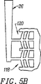
あるいは、図5Bの部分平面図に示すように、アクチュエータ118および120は、変位可能部材26の同じ側面に配置され得る。この構成において、変位可能部材26は、アクチュエータ118のみを始動することによって、入口ポート20を開くように変位し得る。1つのアクチュエータのみを利用することによって、力が半分になり、変位可能部材26の変位が半分になる。しかし、この構成の利点として、アクチュエータ118が受動的に冷却され、その初期位置に戻る前に、変位可能部材26が、アクチュエータ120を始動することによって、入口ポート20を閉じるように変位され得ることがある。これは、変位可能部材の反対側にアクチュエータを有し、アクチュエータの受動的冷却に依存して変位可能部材をその閉位置に変位する構成と対照的である。
【0043】
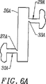
図6A〜6Dに、アクチュエータ(単数または複数)の他の変形例を示す。図6Aに示すように、変位可能部材26Aは、要素29Aおよび31Aによって浮遊し得る。要素29Aおよび31Aのいずれか、または両方は、膨張可能アクチュエータとして機能を果たし得る。例えば、アクチュエータ要素29Aは、始動の際に、変位可能部材26Aに向かって膨張し、アクチュエータ要素29Aは、アンカー要素31Aの周りに部材26Aを変位する。要素29Aおよび31Aの両方が膨張可能アクチュエータとして機能を果たす場合、両方の要素29Aおよび31が、変位可能部材に沿って、要素29Aおよび31の中程に関して、ピボットポイントの周りで、アクチュエータ要素の膨張の程度に依存して、部材26Aを変位する。言うまでもなく、要素29Aおよび31の両方がアクチュエータとして機能を果たす場合でも、いずれの要素も、他の要素を始動することなく、始動され得る。好適には、要素29Aおよび31は、それぞれ、先細り部分33Aおよび37Aを規定して、変位可能部材26Aの変位を容易にする。
【0044】
あるいは、図6Bに示すように、変位可能部材26Bは、要素29Bによって、且つ、変位可能部材の遠位端部31Bによって、浮遊し得る。好適には、要素29Bのみが、動作の際に変位可能部材26Bに向かって膨張して部材26Aを遠位端部31の周りで変位させるような、膨張可能アクチュエータとして機能を果たす。しかし、好ましくはないが、遠位端部31Bが、また、膨張アクチュエータとして機能を果たし得る。言うまでもなく、要素29Bおよび遠位端部31Bの両方がアクチュエータとして機能を果たす場合でも、いずれの要素も、他の要素を始動することなく、始動され得る。好適には、要素29Bは、先細り部分33Bを規定して、要素29Bに関しての変位可能部材26Aの変位を容易にする。さらに、変位可能部材26Bは、好適には、また、変位可能部材26Bの断面の面積が遠位端部31Bに向かって低減するように、遠位端部31Bで先細り部分37Bを規定する。
【0045】
次に、図6Cを参照すると、変位可能部材26Cが、延長アーム39および41を備える1つのアクチュエータ29Cによって浮遊し得る。延長アーム39および41は、異なる断面の面積を有し、例えば、延長アーム39の断面の面積は、延長アーム41の断面の面積よりも小さい。断面の面積の差のため、延長アーム39の抵抗はより大きく、始動の際の熱膨張は、延長アーム41の熱膨張より大きい。従って、アクチュエータ29Cの始動の際、変位可能部材26Cは、延長アーム39によって、延長アーム41によってと比較すると、より遠くに変位されて、部材26Cが、方向D43に線形に変位し、延長アーム41および変形可能部材26Cの交差する部分に近いピボットの周りを回転する。図示していないが、延長アーム39および41のいずれか、または両方が、先細り部分を設けて、変形可能部材26Cの変位を容易にする。この変形例において、延長アーム39および41、ならびに変形可能部材26Cはドープされ、そこを流れる電流の印加およびフローを可能にする。
【0046】
図6Dに示すように、変位可能部材26Dは、部材26のいずれかの側面に配置されている、2つのアクチュエータ29Dおよび31Dによって浮遊し得る。アクチュエータ29Dは、延長アーム39’の断面の面積が延長アーム41’の断面の面積よりも小さいような、異なる断面の面積を有する、延長アーム39’および41’を備える。同様に、アクチュエータ31Dは、延長アーム39’’の断面の面積が延長アーム41’’の断面の面積よりも小さいような、異なる断面の面積を有する、延長アーム39’’および41’’を備える。延長アーム39および39’ならびに/あるいは延長アーム41および41’は、同じ断面の面積を有していてもよいし、有していなくてもよい。上述したように、断面の面積の差のため、延長アーム39’および39’’の抵抗がより大きく、始動の際の熱膨張は、それぞれ、延長アーム41’および41’’の熱膨張よりも大きい。
【0047】
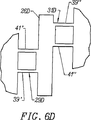
さらに、アクチュエータ29Dおよび31Dが、好適には、延長アーム41’が、延長アーム39’’よりも延長アーム41’’に近く、延長アーム41’’が延長アーム39’よりも延長アーム41’に近くなるように、配置される。従って、アクチュエータ29Dおよび31Dの始動の際に、変位可能部材26Dは、延長アーム39’および39’’によって、延長アーム41’および41’’によってと比較すると、より遠くに変位されて、部材26Dが、アクチュエータ29Dおよび31Dのほぼ中間点にあるピボットの周りを回転する。図示していないが、延長アーム39’、39’’、41’および41’’のいずれか、または全てが、先細り部分を設けて、変形可能部材26Cの変位を容易にする。図6Cに示した変形例と同様に、延長アーム39’、39’’、41’および41’’、ならびに変形可能部材26Dはドープされ、そこを流れる電流の印加およびフローを可能にする。
【0048】
本発明のさらに別の実施形態において、1つ以上のセンサ(図示せず)が、変位可能要素に一体的に固定され得る。センサは、例えば、変位の間に曲がる場合、変位可能部材内のストレスの変化の発生の際に、電気的特性を変化させるピエゾ抵抗器のようなデバイスであり得る。ピエゾ抵抗器は、リブの側面の表面上に位置され得る。ピエゾ抵抗器の電気的特性の変化が利用されて、変位可能部材の変位または移動を感知し得る。
【0049】
明らかなように、圧電アクチュエータ、静電性アクチュエータ、または気圧アクチュエータのような、熱または他のタイプのアクチュエータの数多くの他の構成のうち、集積および変位可能部材にもっとも適するものが、本発明のマイクロバルブ10に容易に適用および採用されて、第2のストッパー端部42の変位が達成され得る。例えば、図1のマイクロバルブの2つのアクチュエータのうちの1つは、変位可能部材をつなぎ留め、且つ/または回転させる1つのビームによって変位され得る。変位可能部材は、従って、回転の中心、あるいは変位可能部材に沿って、固定されたビームとアクチュエータのシャフトとの間のほぼ中程にあるピボットの周りを回転し得る。従って、変位可能部材は、アクチュエータのみの熱始動によって、開位置と閉位置との間で変位可能であり得る。
【0050】
次に図7を参照すると、マイクロバルブ10’の第3の層16が、流体の圧力の均衡をとる第2の入口ポート52を規定する、代替的な実施形態の断面図が示されている。入口ポート20および第2の入口ポート52は、従って、変位可能部材26が閉位置または開位置と閉位置との間にある場合、流体がストッパー端部42の反対側の表面に衝突するように、流体をキャビティに導入し得る。これは、少なくとも部分的に、キャビティ24に入る流体から得られる、変位可能部材に及ぼされる流体圧力を補償するか、または均衡をとる。ストッパー端部42に及ぼされる流体圧力は、マイクロバルブ10’が入口ポート20と垂直に並ぶ領域に配置されるように、マイクロバルブ10’がドーズされた位置または開位置と閉位置との間にある場合に発生する。流体が入口ポート20を流れるので、流体は、第1の層12に隣接するストッパー端部42の表面に衝突し、圧力を及ぼし、キャビティ24内に入る。この好適な実施形態の変位可能部材26は、変位可能部材26がシリコンから製造されている場合、約300〜500psiの流体圧力に耐え得るので、変位可能部材26のストッパー端部42に及ぼされる流体圧力について補償することが望ましい。しかし、完全な補償は、シリコンのような材料の固有の強度が比較的小さい圧力の不均衡に容易に耐え得るので、不必要である。従って、向かい合わせの第2の入口ポート52を設けることによって、マイクロバルブ10は、数千psiの流体圧力に耐え得る。
【0051】
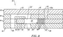
図8は、変位可能部材26上の垂直入射流体力を補償するか、または均衡をとる入口チャネル56および第2の入口ポート52’を含む他の代替的な実施形態の断面図である。入口チャネル56は、第1、第2、および第3の層12、14、および16を通じて伸びており、第2の入口ポート52を通じてキャビティ24にフローを方向付ける。従って、流体は、マイクロバルブ10’’の第1の層12を通じて導入され得、反対の方向から、キャビティ24に導入されるように方向付けられ得る。第4の層54が設けられて、第3の層16の上を入口通路56をおおい、第3の層が第2の層および第4の層14および54の間になるように配置される。
【0052】
次に、図9〜13の平面図を参照すると、流体衝突力に起因する流体圧力に加えて、変位可能部材26のストッパー端部42が、また、入口流体フローフェース58の局地的な流体力、ならびに流体摂動にさらされる。フェース58の局地的な力は、流体が入口ポート20および/または第2の入口ポート52を通じてキャビティ24に入るので、流路が曲がることによって引き起こされる。この力によって、変位可能部材26が、流体力が方向付ける方向に変位するように刺激される。従って、変位可能部材の動きと共に、局所力の低減について、ならびに同じ平面における流体摂動について、補償することが、また、望ましい。
【0053】
図9〜13に、流体力の補償を得る様々な方法および構成を示す。図9〜13に示す実施形態の各々は、入口ポート20から出口ポート22に流れる流体が衝突して、変位可能部材26を流体が及ぼす結合力にかける、流体力結合表面を含む。結合力は、フェース58とは異なる表面への流体フローの衝突(図9および10に示す実施形態)、あるいは、流体フローをフェース58に向かって再度方向付けるか、またはは少なくとも摂動すること(図11〜13に示す実施形態)のいずれかによって、引き起こされる。
【0054】
図9に示すように、変位可能部材26aは、さらに、通常U型拡張部分60を備えて、P型変位可能部材26aを形成する。U型拡張部分60は、出口ポート22を少なくとも部分的に囲むか、または密閉する。流体フローは、ストッパー端部42の表面58上の局所的な力を、少なくとも部分的に補償するか、または、均衡をとるように、U型拡張部分60に力を及ぼす。U型拡張部分60は、さらに、変位可能部材のストッパー端部42と拡張部分60との間の流体フローを囲み、そのことによって、また、マイクロバルブの流体の漏れを減少する。最終用途によって、囲いの外側の圧力が比較的一定になることがさらに可能になり、囲いの外側の領域からの圧力が低くなるか、正味の圧力が無くなる。拡張部分60の他の適切な形、例えば、L型変位可能部材が利用されて、h型変位可能部材(図示せず)が形成され得る。
【0055】
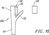
あるいは、図10に示すように、変位可能部材26bは、出口22を囲むのではなく、入口20と出口22との間に配置される拡張部分62を備え得る。拡張部分62は、ストッパー端部42のフェース58上の局所的な力を、少なくとも部分的に、補償するか、または均衡をとるため、流体フローが拡張部分62に力を及ぼすように、流体フローを再度方向付ける。
【0056】
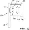
図11〜13に示すように、第1の層12および/または第3の層16に固定された1つ以上の部材が、キャビティ24内に、代替的にまたは付加的に設けられて、ストッパー端部42のフェース58上の局所的な力を、少なくとも部分的に、補償するか、または均衡をとる。図11に示すように、部材64は、キャビティ24内に設けられ得、変位可能部材26aは、その中の流体フローを囲む拡張部分60を備え得る。拡張部分60および部材64の組み合わせによって、変位可能部材26aでの流体フローを再度方向付けることなしに、力が補償され得る。あるいは、バッフル66が、図12に示すように、カーブした表面を備え得、フェース58に向かうフローを再度方向付け、そのことによって、力を補償する。図13に、流体力を補償するか、または均衡をとるように、バッフル70の周りのフローを再度方向付ける、カーブバッフル68およびバッフル70を有するマイクロバルブを示す。
【0057】
図14は、角度のある出口72および角度のある入口20aが流体フロー補償部材として機能を果たす、本発明のさらに他の実施形態の例示する図面である。角度のある出口72および角度のある入口20aは、部分的に他の層73によって部分的に規定されているように、図14に示されているが、第1の層12によってのみ規定されてもよい。流体は、角度のある入口20aを通じて、入口角度αの、矢印74によって示される方向で、キャビティ24に流れ込み、流体は、出口角度φの、矢印76によって示される方向で、キャビティ24から流出する。入口角度αは、変位可能部材26のストッパー端部42の変位によって制御されるが、出口角度φは概して一定である。流体入口および出口角度αおよびφは、流体力の均衡をとるように選択される。従って、流出角度φでの流体流出フローは、入口角度αでの流体入口フローによって及ぼされる力に対して均衡をとる力を及ぼす。
【0058】
次に、図15を参照すると、本発明による、マイクロバルブ78のさらに他の代替的な実施形態の断面図が示されている。マイクロバルブ78は、気体バルブとして利用され得る。気体バルブ78について、変位可能バルブが閉位置にある場合の凹部18とストッパー端部42との間隔は、流体マイクロバルブ10について、好適には、0.5μmより少ない間隔である。気体の漏れは、流体バルブの場合と異なり、流体の張力によっては低減されないので、間隔を最小化することによって、気体の漏れが防がれるか、または最小化される。間隔の大きさは、第1の層12および/または第3の層16の凹部18の深さを低減することによって、低減される。
【0059】
付加的にまたは代替的に、間隔の大きさは、変位可能部材26のストッパー端部42の入口表面にフランジ80を設けることによって、さらに低減され得る。フランジ80は、変位可能部材26が閉位置にある場合、ストッパー端部42の入口表面と入口20bとの間のシールを強める。好適には、入口チャネル79は、第1および第2の層12および14を通じて設けられて、気体がキャビティ24に第2の層14の平面と平行な方向で流れ込むように、気体フローを入口ポート20bを通じてキャビティ24に方向付ける。入口ポート20bは、第2の層14の平面に対して概して垂直なキャビティ24の側壁にそって規定される。従って、第2の層14の平面における変位可能部材26の入口20を閉じる変位は、また、フランジ80に入口20に対するより良好なシールを形成させる。
【0060】
本発明のこの実施形態のマイクロバルブの製造は、シリコン融解結合、および深い反応のイオンエッチング(DRIE)のような融解結合を含む。
【0061】
溶融結合は、一方のシリコン層の他方のシリコン層への結合を可能にし、ある単一の機械的構造を形成する。溶融結合は、分子レベルにおいてであることが実証されており、非常に高い機械的剛性を提供する。溶融結合技術は周知である。例えば、K.E.Petersen、D、Gee,F.Pourahmadi、R.Craddock、J.BrownおよびL.Christalの、「Surface Micromachined Structures Fabricated with Silicon Fusion Bonding」(Proceedings,Transducers91、1992年6月、397〜399頁)を参照のこと。この文献は、本明細書中で参考として明確に援用される。
【0062】
本発明の好ましい実施形態に従うシリコン微細構造を作製するプロセスは、図16a〜fを参照して説明される。本実施形態は、3つのシリコンウエハを使用する。3つのシリコンウエハを使用して、本プロセスにより第2のウエハの一体部分(第2の層14に相当する)として規定した単結晶シリコン構造(SCS)微細構造が形成する。第1のウエハ(第1の層12に相当する)および第3のウエハ(第2の層16に相当する)は、第2のウエハのキャリアとして機能する。あるいは、このキャリアは、例えばガラス(Pyrex)から形成され得る。以下の議論は3つのウエハについて言及しているだけであるが、これらの原理は2つ以上のウエハのスタックを含む微細構造の形成に適用できることが、もちろん理解される。
【0063】
図16aにおいて、第1のウエハはフォトレジストでパターン化され、そこに形成される窪んだ領域を規定し、そしてその窪んだ領域は、例えばプラズマエッチング、KOHまたは他のシリコンエッチャントでのウエットエッチング、あるいは示差酸化物成長法(differential oxide growth)などの標準的な半導体技術を使用して形成される。窪んだ領域は、任意の形状を有し得、そして例えば、0.1μm未満〜100μmを越えての任意の要求された深さを有し得る。本実施態様では、この窪んだ領域は、約1μmの深さである。
【0064】
窪んだ領域は、単一の一様な深さである必要はないことが理解されるべきである。例えば、いくつかの標準的なシリコンエッチング工程が、種々の機械的機能について使用され得るいくつかの種々の深さを生成するために使用され得る。あるいはまたはさらに、上記のように、第2の層が第1の層12および第3の層16からインデントが付けられ(示されず)、それらの間にクリアランスを提供することがさらに理解されるべきである。その上、第1のウエハ表面および第3のウエハ表面のそれぞれは、裸シリコンであるか、酸化物層でコートされているかのいずれかであり得る。さらに、窪んだ領域の基盤は、裸シリコン、酸化シリコン、ドープしたシリコン、または次のウエハの結合工程および温度処理工程に絶え得る任意の他の薄膜でコートされ得るかのいずれかであり得る。
【0065】
図16bに示されるように、次いで入口ポートが第1のウエハを介してエッチングされる。示されてはいないが、出口ポートが同時に第1のウエハを介してエッチングされ得る。あるいはまたはさらに、出口ポートは第3のウエハを介してエッチングされ得る。
【0066】
図16cにおいて、第1のウエハのパターン化された表面は、シリコン溶融結合(すなわち、直接結合)プロセスにより、第2のウエハに結合される(好ましくはドープされる)。溶融結合技術は周知である。例えば、K.E.Petersen、D、Gee,F.Pourahmadi、R.Craddock、J.BrownおよびL.Christelの、「Surface Micromachined Structures Fabricated with Silicon Fusion Bonding」(Proceedings,Transducers91、1991年6月、397〜399頁)を参照のこと。この文献は、本明細書中で参考として明確に援用される。本発明の好ましい溶融結合技術では、第1のウエハおよび第2のウエハは親水性にされる。すなわち、それらは薬剤(例えば、熱硝酸または熱硫酸、および過酸化水素溶液または他の強酸化剤(これらは、水がそれらに付着するようにする))で処理される。乾燥後、次いで2つのウエハが、約1時間の間、400℃〜1200℃の温度で、酸化雰囲気中に置かれる。
【0067】
上記のシリコン溶融結合技術は、単結晶シリコンウエハとは異なる熱膨張係数を有し得る中間接着性物質を使用することなく、第1のウエハおよび第2のウエハを共に結合する。さらに、溶融結合は、ウエハの一方または両方の結合した表面に、酸化層または窒化層が形成されて、実行される。
【0068】
溶融結合の代替として、例えば、第1のウエハおよび第2のウエハは、フォトレジストなどの接着剤で共に接着され得る。別の代替として、第1のウエハおよび第2のウエハは、それらの表面の大部分が金などの金属層で覆われ、互いにウエハをアロイ化して使用される。ガラスキャリアが第1のシリコンウエハの代わりに使用される場合において、第2のウエハはこのようなガラスキャリアにアノード的に結合され得る。
【0069】
必要であれば、第2のウエハは、特定の用途で要求される厚みにまで薄くされ、そして磨かれる。あるいは、電気化学的エッチング(ECE)が、ウエハを薄くするために使用され得る。拡散ヒータが、拡散により第2の層14の平坦な表面へ導入され得る。さらに、任意の必要な回路または他の薄膜堆積物およびパターン化処理が、標準的なシリコンプロセシング技術を使用して実施され得る。
【0070】
次いで、第2のウエハは、エッチングされるべきウエハの領域を規定する深度反応性イオンエッチング(DRIE)のためにパターン化される。DRIE技術は、ますます周知となる。例えば、A.A.Ayon、C.C.Lin、R.A.BraffおよびM.A.Schmidtの、「Etching Characteristics and Profile Control in a Time−Multiplexed ICP Etcher」、Proceedings of Solid State Sensor and Actuator Workshop、Hilton Heat Island、「Highly Anisotropic Selective Reactive Ion Etching of Deep Trenches in Silicon」、Microelectronic Engineerring、第23巻、1994年、373〜376頁;C.Linder.T.Tschan、N.F.de Rooijの、「Deep Dry Etching Techniques as a New IC Compatible Tool for Silicon Micromachining」、Proceedings、Transducers’91、1991年6月、524〜527頁;C.D.FungおよびJ.R.Linkowskiの、「Deep Etching of Silicon Using Plasma」、Proceedings of the Workshop on Micromachining and Micropackaging of Transducers、1984年11月7〜8日、159〜164頁;ならびに、J.W.Bartha、J.Greeschner、M.PuechおよびP.Maquinの、「Low Temperature Etching of Si in High Density Plasma Using SF6/O2」、Microelectronic Engineering、第27巻、1995年、453〜456頁を参照のこと。反応性イオンエッチング装置は現在、非常に深い(100ミクロンより深い)ホールまたは溝のエッチングを可能にし、同時に高アスペクト比(エッチングされた領域の深さとエッチングされた領域の幅との間の比)を維持する。この装置は、300ミクロン程度の深さの溝について、少なくとも30:1のアスペクト比が可能であることが分かった。
【0071】
本質的に、DRIEは、化学的エッチングとイオン衝撃との間に相乗作用を含む。衝撃を与えられたイオンは、シリコン表面と化学的に反応する。DRIEプロセスは、シリコンの結晶面または結晶配向に関係なく側方方向よりも垂直方向でずっと速い速度で(すなわち、異方性で)、有利にエッチングする。結果として、相対的に深い実質的に垂直方向の溝またはスロットが、単結晶シリコン(SCS)の第2のウエハに形成される。これらの実質的に垂直方向の溝またはスロットは、ウエハ内の結晶学的な配向とは無関係に、第2のウエハ上の任意の場所で形成され得る。結果として、容量性または静電性プレートのような高アスペクト比構造が形成され、そして円、楕円および螺旋のような任意の輪郭の構造が形成され得る。
【0072】
図16dに示されるように、DRIEプロセスが、第2のウエハを介して完全にエッチングされるように使用され、変位可能部材およびアクチュエータを規定する。DRIEエッチング工程は、第2のウエハに形成された単結晶シリコン(SCS)微細構造を機械的に放出し、これは次いで、第2のウエハに対してかつ第2のウエハの面で移動することが自由になる。20:1以上のアスペクト比(高さ/幅)を有する浮遊されたプレート/梁構造は、下記に記載のDRIEプロセスを使用して製造される。
【0073】
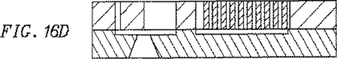
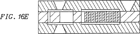
誘導的に結合されたプラズマソースは、マスクとしてフォトレジストまたは二酸化シリコンを使用してシリコンをエッチングする。エッチングされた溝の側壁のソースガスの重合により横方向のエッチングレートが遅くなり、高い異方牲を可能にする。このエッチング化学は、例えば50ミリトルでSF6である。酸素添加ガスおよびSurface Technology Systemsから市販されているフッ化ガスは、高Si/フォトレジストエッチングレート比を提供することを補助する。6ミクロンのフォトレジストは、パターン化マスクとして働く。フォトレジスト感度は約50:1であり、これは、約6μmのレジストを用いて300μmの深さまでエッチングすることが可能となる。Surface Technology Systems(STS)(Redwood City、California)から市販されている「マルチプレックスRIEシステム」は、誘導的に結合したプラズマDRIEを実施するために使用され得る。あるいは、St.Petersburg、FloridaのPlasma Thermから市販されている。
【0074】
溶融結合およびDRIEの組み合わせは、例えば本発明のマイクロバルブのような三次元構造の構成を可能にする。例えば、E.H.Klaassen、K.Petersen、J.M.Noworoski、J.Logan、N.I.Maluf、J.Brown、C.Storment、W.McCulleyおよびG.T.A.Kovacsの、「Silicon Fusion Bonding and Deep Reactive Ion Etching;A New Technology for Microstructures」、Proceeding、Transducers95、Stockholm、Sweden、1995年、556〜559頁を参照のこと。
【0075】
図16eにおいて、第3のウエハのパターン化された表面は、図16cを参照して上記のように、シリコン溶融結合(すなわち、直接接合)プロセスにより、第2のウエハへ結合される。示されてはいないが、結合の前に第3のウエハは、窪んだ領域、入口ポートおよび/または出口ポート、ならびにスルーウエハコンタクトホールまたはバイアを規定する第1のウエハと同様に処理された。
【0076】
図16fに示されるように、アルミニウムのような導電性の材料の層は、例えばスパッタリングでコンタクトホールまたはバイアの表面、コンタクトホールを介して曝された第2のウエハの表面、および第3のウエハの外部平坦表面の少なくとも一部分に堆積される。導電層は、従って、電気的接触を可能にするパッドとアクチュエータとの結合を形成する。任意の必要な回路または他の薄膜堆積およびパターン化処理は、第3のウエハ上で標準的なシリコンプロセシング技術を使用して実施され得る。
【0077】
多くの数の改変が、このプロセスに容易に導入できる。例えば、第1の層12および/または第3の層16は、シリコンの代わりにガラス(Pyrex)から作製され得る。マイクロバルブは、3つ以上のウエハまたは層または から形成され得、微小機械デバイスは、2つ以上のウエハまたは層から形成され得る。さらに、浅いキャビティは、第1の層12および第3の層16の代わりにまたはそれらに加えて、第2の層14に規定され得る。あるいは、それぞれの層は、別々に処理され、次いで提携した結合工程で組み立てられ得る。明らかなように、当業者は、例えば単にレイアウトを変えるだけで、製造工程に対するこれらのおよび多数の他の改変を容易に為すことができる。
【0078】
本発明のマイクロバルブは、以下に記載のようにアンチロックブレーキシステム、インクジェット印刷、冷蔵、大きなバルブ用のパイロット(例えば、オートマチックトランスミッションおよび大きな工業用バルブ)での使用に適合され得る。
【0079】
ここで、図17を参照すると、マイクロバルブ82はさらに、一つの出口22へ流体が流れるための2つの入口ポート84、86を選択的に制御するように適合され得る。入口ポート84、86の開口部および閉鎖部は相互に依存する。マイクロバルブ82の他の詳細は、他の図を参照して上記の記載から理解される。特に、作動すると、マイクロバルブ82は、入口バルブ86を閉じたままにしながら入口バルブ84を開けるように制御され得る。その逆も同様である。マイクロバルブ82はまた、入口バルブ84、86の両方を部分的に開けるように制御され得る。従って、マイクロバルブ82は、1つまたは2つの流体ソースから流体フローを選択するように使用され得る。
【0080】
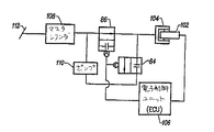
明らかなように、多数の他の流体フロー制御統合が、本発明のマイクロバルブで達成され得る。例えば、本発明の単一の一体化マイクロバルブ87は、従来のアンチロックブレーキシステムの各ホイールに利用される通常開(N.O.)および通常閉(N.C.)のソレノイドバルブを置き換えて利用され得る。単一の一体化マイクロバルブを利用するアンチロックブレーキシステム100の一部の模式図、およびこのような単一の一体化マイクロバルブ87の部分模式図が、図18および19にそれぞれ示される。
【0081】
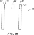
アンチロックブレーキシステム(ABS)は、乗用車において非常に一般的になった。図18に示されるように、アンチロックブレーキシステム100は一般に、ホイール102の速度を感知するホイール速度センサ(示されず)、ホイール102のブレーキキャリパ104へのおよびブレーキキャリパ104からのブレーキフルードの流れを制御するための通常開(N.O.)バルブ86および通常閉(N.C.)バルブ84、ホイール速度センサからの入力を受容し、信号をマイクロバルブ87へ出力する電子制御ユニット(ECU)106、マスターシリンダ108、ならびにポンプ110を備える。図19に示されるように、マイクロバルブ87は、ブレーキフルードをブレーキキャリパへ向ける一つの出口ポート22、および2つの変位可能部材88、90を規定し、二つの入口ポート84、86をそれぞれ選択的に開閉する。
【0082】
通常開の入口86は、ドライバーがブレーキペダル112に力をかけたときに、ブレーキフルードがマスターシリンダ108からブレーキキャリパ104へ流れることを可能にする。ABSシステムが作動することなく、通常閉の入口88は、ブレークフルードの流動に対して少なくとも実質的に閉であり、そして通常開の入口86は、ドライバーによりブレーキペダル112に力が加えられると、ブレークフルードのブレーキキャリパ104への流動を可能にする。
【0083】
しかし、滑りやすい路面では、タイヤと路面との間の不十分な摩擦またはグリップ力となり得、ドライバーがブレーキペダル112に力を加えると、ブレーキキャリパ104はホイール102をロックする。ブレーキキャリパ104がホイール102をロックし、ホイール102の回転が止まると、ホイール102は、滑りやすい路面に沿って横滑りをし、車の制動距離が増加する。従って、車はその運動量のために動きつづける。本質的に、ブレーキシステムによるホイールのロックは、タイヤと路面との間のグリップ力が、ホイールとブレーキパッドとの間の制止力またはグリップ力よりも小さい場合に起こる。
【0084】
アンチロックブレーキシステムは、適切なレベルの制止力に到達するまで付加されるブレーキフルード圧を制御することにより(すなわち、ホイールと路面との間のグリップ力に等しいレベルにまで制止力を減少させることにより)、ホイールのロックの問題を低減または解消する。アンチロックブレーキシステムは、ホイールがロックしようとするのを感知するホイール速度センサに応答して、起動される。アンチロックブレーキシステムが起動されると、コンピュータはN.O.バルブを閉じる。ホイール速度センサが、N.O.バルブが閉じられた後でさえロックしようとするホイールを感知しつづけると、コンピュータはN.C.バルブを開け、いくらかのブレーキフルードをホイールシリンダまたはキャリパからマスターシリンダへとポンピングする。N.C.バルブは開閉状態を繰り返し、コンピュータがブレーキが制御されていると判断するまで(すなわち、ホイール速度センサがホイールがもはやロックしようとはしないと感知するとき)、ブレーキフルードの流動を制御する。反復したN.C.バルブの開閉により、フルード流動制御が比例的に達成される。アンチロックブレーキシステムは、ブレーキペダルが踏まれ続けているときにだけ達成される。
【0085】
自動車または乗用車の従来のアンチロックブレーキシステムは、ブレーキフルードの流動を制御するために1つの車輪あたり2つのソレノイドバルブを使用するので、典型的な四輪乗用車について8つのソレノイドバルブを使用することになる。しかし、ソレノイドバルブの使用は、上記のようにいくつかの欠点がある。比例ソレノイドバルブが使用可能であるが、アンチロックブレーキシステムに使用されるコスト効率のよいソレノイドバルブは、単にオンおよびオフ(バイナリ)スイッチングを行い、従って、正確な所望のレベルのフロー制御を得るようにバルブにパルスが与えられることが必要となる。このようなパルスを、所望でないかもしれないがブレーキペダルを踏み続けているときにドライバーが感知することができる。
【0086】
図19に示されるようなマイクロバルブ87は、従来のアンチロックブレーキシステムの2つのソレノイドバルブを置き換えて使用され得る。それぞれの変位可能部材88、90は、それぞれのサーマルアクチュエータにより別々に制御される。しかし、アンチロックブレーキシステムにおいて、変位可能部材88、90は、同時に両方ともが開の位置であるわけではない。従って、通常のブレーキ操作の間、(入口84に対して通常閉の位置にある)変位可能部材88が閉の位置にある間、(入口86に対して通常開の位置にある)変位可能部材90は開の位置にある。このように、通常のブレーキ操作の間にドライバーがブレーキペダル112を踏むと、ポンプ110がブレーキフルードをマスターシリンダ108からブレーキキャリパ104へ通常開の入口86を通ってポンピングする。
【0087】
ECU106が、ホイール102が所定の閾値を超えるのを感知すると、ECU106は信号をマイクロバルブ87へ送信して変位可能部材90を入口86に対して閉の位置にまで変位し、かつ変位可能部材88をその閉の位置から入口84に対して開位置と閉位置との間の位置にまで変位する。変位可能部材88を入口84に対して開位置と閉位置との間の位置にまで変位することにより、所望のレベルのブレーキフルードがポンプ110によりブレーキキャリパ104からマスターシリンダ108へと除去されることが可能となる。従って、一つの一体化マイクロバルブだけが2つの従来のバイナリソレノイドバルブを置き換えるために使用される。
【0088】
変位可能部材88は、好ましくは開閉位置の間でパルスされず、そしてブレーキキャリパ104からポンピングされる所望の量のブレーキフルードを正確に制御する開閉位置の間の位置に変位されることが好ましい。しかし、変位可能部材88は、比例的な流体フロー制御を達成するために、入口84に対して開閉位置の間でパルスされ得る。
【0089】
本発明の特定の実施形態が記載され、図示されるが、本発明の意図から逸脱することなくこれらの実施形態の改変が為され得ることが理解される。従って、本発明は上記の特許請求の範囲で規定されることが意図される。
【図面の簡単な説明】
【図1】 図1は、本発明の提示する実施形態の比例するマイクロバルブの第1、第2および第3の層の分解斜視図である。
【図2】 図2は、図1の3−3線での断面図である。
【図3】 図3は、プレートまたはリブを有するアクチュエータの平面図である。
【図4】 図4は、アクチュエータの代替的な構造の平面図である。
【図5A】 図5Aは、アクチュエータの代替的な構造の平面図である。
【図5B】 図5Bは、アクチュエータの代替的な構造の平面図である。
【図6A】 図6Aは、アクチュエータの代替的な構造の平面図である。
【図6B】 図6Bは、アクチュエータの代替的な構造の平面図である。
【図6C】 図6Cは、アクチュエータの代替的な構造の平面図である。
【図6D】 図6Dは、アクチュエータの代替的な構造の平面図である。
【図7】 図7は、流体が反対側から入って圧力の均衡をとる、第2の入口ポートを有するマイクロバルブの断面図である。
【図8】 図8は、流体が反対側から入って圧力の均衡をとる、第2の入口ポートを有する他のマイクロバルブの断面図である。
【図9】 図9は、流体力を補償する拡張部分を含む変位可能部材を示す部分平面図である。
【図10】 図10は、流体力を補償する拡張部分を含む変位可能部材を示す部分平面図である。
【図11】 図11は、流体フローを再度方向付ける、1つ以上のバフルおよび拡張部分をさらに含む、本発明のマイクロバルブを示す部分平面図である。
【図12】 図12は、流体フローを再度方向付ける、1つ以上のバフルおよび拡張部分をさらに含む、本発明のマイクロバルブを示す部分平面図である。
【図13】 図13は、流体フローを再度方向付ける、1つ以上のバフルおよび拡張部分をさらに含む、本発明のマイクロバルブを示す部分平面図である。
【図14】 図14は、角度のある出口ポートを有するマイクロバルブの部分断面図である。
【図15】 図15は、本発明の比例する気体マイクロバルブの断面図である。
【図16a】 図16aは、本発明による製造プロセスの流れを示す図である。
【図16b】 図16bは、本発明による製造プロセスの流れを示す図である。
【図16c】 図16cは、本発明による製造プロセスの流れを示す図である。
【図16d】 図16dは、本発明による製造プロセスの流れを示す図である。
【図16e】 図16eは、本発明による製造プロセスの流れを示す図である。
【図16f】 図16fは、本発明による製造プロセスの流れを示す図である。
【図17】 図17は、出口ポートへの流体フローを制御する2つの入口ポートを開閉する変位可能部材の平面図である。
【図18】 図18は、バルブの利用の実例であるアンチロックブレーキシステムの一部の模式的な図である。
【図19】 図19は、出口ポートへの流体フローを制御する2つの入口ポートを独立して開閉する2つの変位可能な部材を有するマイクロバルブの平面図である。[0001]
(Background of the Invention)
(1. Field of the Invention)
The present invention relates generally to semiconductor electromechanical microdevices, and more particularly to microdevices having high aspect ratio geometries and members that are displaceable with respect to a transducer.
[0002]
(2. Explanation of related technology)
A fluid valve generally includes a fluid port, an actuator, and a movable valve structure that opens and closes the fluid port in response to the actuator. There are many types of fluid valves. Examples of fluidic valves include solenoid valves and microvalves made from microfabricated semiconductor materials, such as bimetallic microvalves and encapsulated fluidic microvalves. However, there are many problems with each of these valve or microvalve types.
[0003]
Solenoid valves utilize a coil in the form of a cylinder and generally have a core that can be drawn into the cylinder by a magnetic field that is triggered when current flows through the coil. Solenoid valves are typically used, for example, in conventional antilock braking systems. However, solenoid valves are usually relatively large and heavy. Furthermore, electromagnetic valves, such as solenoid valves, often require relatively high currents and can cause voltage supply spiking. The solenoid valve can also represent hysteresis, thereby representing a non-linear response to the electronic input. Furthermore, the operation of an electromagnetic valve, such as a solenoid valve, can be relatively slow due to the relatively long lag time between the delivery of current to such a valve and the resulting magnetic field and corresponding force. . Also, it is difficult to open or close the solenoid valve only partially, so the solenoid valve is typically used as an on / off valve rather than as a proportional valve.
[0004]
An exemplary bimetallic microvalve utilizes an actuator manufactured from two materials having different coefficients of thermal expansion. Due to the difference in coefficient of thermal expansion, when the actuator is heated or cooled, the actuator bends or straightens, thereby opening and closing the flow orifice. US Pat. No. 5,058,856 discloses such a bimetallic microvalve having first and second substrates. The first substrate defines a flow orifice and a valve seat. The second substrate defines a valve face aligned with the flow orifice and defines a movable actuator. The movable actuator includes first and second layers of material having substantially different coefficients of thermal expansion, such as a silicon layer and a nickel layer. The actuator also includes a heating element and is secured at one end so that selective heating causes the actuator to bend due to differences in the coefficient of thermal expansion. Bending of the actuator causes the valve face to disengage from the valve seat or toward the valve seat to open and close the valve, thereby controlling the fluid flow through the orifice.
[0005]
However, one of the problems associated with such a bimetallic microvalve is that the actuator is started in response to a change in temperature, so that an unintentional start of the microvalve may occur due to a change in outside air temperature. In addition, because the heated element, i.e., the actuator, is in contact with the fluid flow, it can provide undesirable heating to the fluid in the fluid path, cool the heater, and displace the actuator. Furthermore, the actuator displacement is also relatively small, typically on the order of 10 ppm / ° C.
[0006]
An example of an encapsulated fluid microvalve is disclosed in US Pat. No. 4,824,073. An encapsulated fluid microvalve utilizes the principle of expansion and pressurization of a volume of fluid or gas in a sealed cavity when heated to deform a flexible membrane or diaphragm that forms one or more walls of the cavity. When the encapsulated fluid or gas is heated, the diaphragm is deformed to open and close the ports and control the fluid flow through the fluid orifice. The heating of the encapsulated fluid or gas is accomplished by a resistive heating element in the cavity so that current flows through the resistive element and generates heat that heats the fluid or gas.
[0007]
An encapsulated fluid microvalve can generate a relatively large force and can be used, for example, as a mass fluid controller to control a large fluid flow. Further, the encapsulated fluid microvalve may also operate in proportion to provide a proportional range of fluid control. That is, the valve can be controlled to adjust the rate of fluid flow through the valve according to the magnitude of the control signal.
[0008]
However, encapsulated fluid microvalves have a relatively slow response time due to the time required to heat and cool the fluid. Furthermore, the deformation membrane of the encapsulated fluid microvalve is in contact with the fluid or gas flow path. Thus, the deformation temperature of the membrane can affect the temperature of the fluid or gas in the flow path, and the temperature of the fluid or gas in the flow path can affect the temperature of the deformation film.
[0009]
Furthermore, none of the above valves provide flow-force and / or pressure-force compensation that minimizes the effect of fluid flow through the microvalves.
[Patent Document 1]
Japanese Patent Publication No.49-039223 December 1974
[Patent Document 2]
Patent Publication No.49-039224 December 1974
[Patent Document 3]
Japanese Patent Publication No. 49-048264, October 1974
[Patent Document 4]
Japanese Patent Publication No.49-048265 October 1974
[Patent Document 5]
Japanese Patent Publication No. 06-56014 March 1994
[Patent Document 6]
Japanese Patent Publication No. 06-286600 October 1994
[Patent Document 7]
Japanese Patent Publication No.59-2175, January 1984
[Patent Document 8]
Japanese Patent Publication No.59-2175, January 1984
[Patent Document 9]
U.S. Pat. No. 3,747,628 July 1973
[Patent Document 10]
U.S. Pat. No. 3,860,949 January 1975
[Patent Document 11]
US Pat. No. 4,0054,554 January 1977
[Patent Document 12]
U.S. Pat. No. 4,019,388 April 1977
[Patent Document 13]
US Patent No. 4023725 May 1977
[Patent Document 14]
U.S. Pat. No. 4,152,540 May 1979
[Patent Document 15]
U.S. Pat. No. 4,181,249 January 1980
[Patent Document 16]
US Pat. No. 4,298,023 November 1981
[Patent Document 17]
U.S. Pat. No. 4,341,816 July 1982
[Patent Document 18]
US Patent No. 4434813 March 1984
[Patent Document 19]
US Pat. No. 4,581,624 April 1986
[Patent Document 20]
US Pat. No. 4,628,576 December 1986
[Patent Document 21]
U.S. Pat. No. 4,647,003 March 1987
[Patent Document 22]
U.S. Pat. No. 4,661,835 April 1987
[Patent Document 23]
US Pat. No. 4,772,935 September 1988
[Patent Document 24]
US Pat. No. 4,822,1997 April 1989
[Patent Document 25]
U.S. Pat. No. 4,824,073 April 1989
[Patent Document 26]
U.S. Pat. No. 4,826,131 May 1989
[Patent Document 27]
U.S. Pat. No. 4,828,184 May 1989
[Patent Document 28]
U.S. Pat. No. 4,869,282 September 1989
[Patent Document 29]
U.S. Pat. No. 4,938,742 July 1990
[Patent Document 30]
U.S. Pat. No. 4,943,032 July 1990
[Patent Document 31]
US Pat. No. 4,959,581 September 1990
[Patent Document 32]
US Pat. No. 4,966,646 October 1990
[Patent Document 33]
U.S. Patent No. 5029805 July 1991
[Patent Document 34]
US Pat. No. 5,037,778 August 1991
[Patent Document 35]
US Pat. No. 5,050,838 September 1991
[Patent Document 36]
US Pat. No. 5,054,522 October 1991
[Patent Document 37]
US Pat. No. 5,058,856 October 1991
[Patent Document 38]
US Pat. No. 5,061,914 October 1991
[Patent Document 39]
US Pat. No. 5,064,165 November 1991
[Patent Document 40]
US Pat. No. 5,065,978 November 1991
[Patent Document 41]
US Pat. No. 5,066,533 November 1991
[Patent Document 42]
US Pat. No. 5,069,419 December 1991
[Patent Document 43]
US Pat. No. 5,074,629 December 1991
[Patent Document 44]
US Pat. No. 5,082,242 January 1992
[Patent Document 45]
US Pat. No. 5,096,643 March 1992
[Patent Document 46]
U.S. Pat. No. 5,116,457 May 1992
[Patent Document 47]
US Pat. No. 5,131,729 July 1992
[Patent Document 48]
US Pat. No. 5,133,379 July 1992
[Patent Document 49]
US Pat. No. 5,142,781 September 1992
[Patent Document 50]
US Pat. No. 5,161,774 November 1992
[Patent Document 51]
US Pat. No. 5,169,472 December 1992
[Patent Document 52]
US Pat. No. 5,176,358 January 1993
[Patent Document 53]
US Pat. No. 5,177,579 January 1993
[Patent Document 54]
US Pat. No. 5,178,190 January 1993
[Patent Document 55]
US Pat. No. 5,179,499 January 1993
[Patent Document 56]
US Pat. No. 5,180,623 January 1993
[Patent Document 57]
U.S. Pat. No. 5,1975,17 March 1993
[Patent Document 58]
US Pat. No. 5,209,118 May 1993
[Patent Document 59]
US Pat. No. 5,215,244 June 1993
[Patent Document 60]
US Pat. No. 5,216,273 June 1993
[Patent Document 61]
US Pat. No. 5,217,283 June 1993
[Patent Document 62]
US Pat. No. 5,238,223 August 1993
[Patent Document 63]
US Pat. No. 5,244,537 September 1993
[Patent Document 64]
US Pat. No. 5,267,589 December 1993
[Patent Document 65]
US Pat. No. 5,271,431 December 1993
[Patent Document 66]
US Pat. No. 5,271,597 December 1993
[Patent Document 67]
US Pat. No. 5,309,943 May 1994
[Patent Document 68]
US Pat. No. 5,325,880 July 1994
[Patent Document 69]
US Pat. No. 5,333,831 August 1994
[Patent Document 70]
US Pat. No. 5,336,062 August 1994
[Patent Document 71]
US Pat. No. 5,355,712 October 1994
[Patent Document 72]
U.S. Pat. No. 5,368,704 November 1994
[Patent Document 73]
US Pat. No. 5,400,844 March 1995
[Patent Document 74]
US Pat. No. 5,417,235 May 1995
[Patent Document 75]
US Pat. No. 5,445,185 August 1995
[Patent Document 76]
US Pat. No. 5,553,790 September 1996
[Patent Document 77]
US Pat. No. 5,556,703 September 1996
[Patent Document 78]
US Pat. No. 5,577,533 November 1996
[Patent Document 79]
US Pat. No. 5,785,295 July 1998
[Patent Document 80]
US Pat. No. 5,810,325 September 1998
[Patent Document 81]
US Pat. No. 5,838,351 November 1998
[Patent Document 82]
US Pat. No. 5,848,605 December 1998
[Patent Document 83]
US Pat. No. 5,873,385 February 1999
[Patent Document 84]
US Pat. No. 5,909,078 June 1999
[Patent Document 85]
US Pat. No. 5,926,955 July 1999
[Patent Document 86]
U.S. Pat. No. 5,941,608 August 1999
[Patent Document 87]
US Pat. No. 6,019,437 February 2000
[Patent Document 88]
US Pat. No. 6,105,737 August 2000
[Patent Document 89]
US Pat. No. 6,523,560 February 2003
[Patent Document 90]
German Patent No. 2215526 October 1973
[Patent Document 91]
German Patent No. 2,930,779 February 1980
[Patent Document 92]
German Patent No. 4101575 July 1992
[Patent Document 93]
German Patent No. 4417251 November 1995
[Patent Document 94]
German Patent No. 4422942 January 1996
[Patent Document 95]
EP 0250948 January 1988
[Patent Document 96]
European Patent No. 0261972 March 1988
[Patent Document 97]
British Patent No. 2238267 May 1991
[Patent Document 98]
International Patent No. 9916096 April 1999
[Non-Patent Document 1]
Qi, J. and Johnson, W. et al. (Apr. 6-9, 1999) "Flip Chip on Laminate Manufacturability," 1999 International Conference on High Density Packaging and MCMs. Proc. SPEI--Int. Soc. Opt. Eng. (USA), Denver, CO., Pp. 345-352.
[Non-Patent Document 2]
Search Report (Mar. 15, 2000) PCT / US 99/19971.
[Non-Patent Document 3]
Williams, K. R. et al. (Jun. 7-10, 1999). "A Silicon Microvalve for the Proportional Control of Fluids," Transducers '99 Sendai, Japan., Pp. 1804-1807.
[Non-Patent Document 4]
Yunkin, V.A., et al. (1994). "Highly Anisotropic Selective Reactive Ion Etching of Deep Trenches in Silicon," Microelectronic Engineering 23: 373-376.
[Non-Patent Document 5]
Bartha, J.W., et al., (1995). "Low Temperature Etching of Si in High Density Plasma Using SF.sub.6 / O.sub.2," Microelectronic Engineering, 27: 453-456.
[Non-Patent Document 6]
Carpenter Technology Corporation Technical Data sheet for "Carpenter Low Expansion; 42", date Nov. 1980 <http://www.carpenter.idesinc.com/datasheet.asp?e=181&u=eVIEW=PRINTER> (visited on Mar. 28 , 2002).
[Non-Patent Document 7]
Delphi Automotive Systems product brochure (1997). Variable Bleed Solenoid (VBS) for Transmission, copyright 1997.
[Non-Patent Document 8]
Delphi Automotive Systems product brochure (1998). On / Off Transmission Solenoids, copyright 1998.
[Non-patent document 9]
Duffy, James E. (1994). "Automatic Transmission Fundamentals," Modern Automotive Technology, copyright 1994, p. 707.
[Non-Patent Document 10]
Fung, C.D., et al. (Nov. 7-8, 1984). "Deep Etching of Silicon Using Plasma," Proceedings of the Workshop on Micromachining and Micropackaging of Transducers, pp. 159-164.
[Non-Patent Document 11]
Houston, PN et al. (Jun. 1-4, 1999). "Low Cost Flip Chip Processing and Reliability of Fast-Flow, Snap-Cure Underfills," 1999 Electronic Components and Technology Conference. San Diego, CA, pp. 61 -70.
[Non-Patent Document 12]
Jonsmann, J. et al. (Jan. 17-21, 1999). "Compliant Electro-thermal Microactuator" Twelfth IEEE International Conference on Micro Electro Mechanical Systems Orlando, Florida, IEEE Technical Digest entitled IEEE Catalog No .: 99CH36291C pp. 588 -593 ...
[Non-Patent Document 13]
Klaasen, E.H. et al. (1995). "Silicon Fusion Bonding and Deep Reactive Ion Etching; A New Technology for Microstructures," Proc. Tranducers 95 Stockholm Sweden pp. 556-559.
[Non-Patent Document 14]
Konarski, Mark M. (May 31 to Jun. 4, 1998). "Cure Parameter Effects on the Tg and CTE of Flip Encapsulants," 43rd International SAMPE Symposium and Exhibition. Materials and Process Affordability. Keys to the Future. Anaheim, CA , vol. 1 pp. 823-832.
[Non-Patent Document 15]
Linder, C. et al. (Jun. 1991). "Deep Dry Etching Techniques as a new IC Compatible Tool for Silicon Micromachining," Proceedings, Transducers '91 pp. 524-527.
[Non-Patent Document 16]
Madou, Marc (1997). "Scaling Laws, Actuators, and Power in Miniaturization," Chapter 9 In Fundamentals of Microfabrication CRC Press LLC: Boca Raton, FL., Pp. 405-446.
[Non-Patent Document 17]
Noworolski, J.M. et al., (1996) "Process for in plane-and out-of-plane single crystal-silicon thermal conductors" Sensors and Actuators 55 (1): 65-69.
[Non-Patent Document 18]
Ohio State Univesity Chemistry Department brochure page on Marc J. Madou [online]. Ohio State University [retrieved on Dec. 31, 2000]. Retrieved from Internet: <URL: http://www.chemistry.ohio-state.edu/ resource / pubs / brochure / madou.htm>.
[Non-Patent Document 19]
Petersen, K.E. et al. (Jun. 1991). "Surface Micromachined Structures Fabricated with Silicon Fusion Bonding," Proceedings, Transducers '91 pp. 397-399.
[Non-Patent Document 20]
Author Unknown. (Sep./Oct. 1999). "HiTecMetal Group Develops Niche Market for Brazed Laminated Assemblies," Fluid Power Journal 27..
[Non-patent document 21]
Ayon, A.A. et al. (Jun. 1998). "Etching Characteristics and Profile Control in a Time-Multiplexed ICP Etcher," Proc. Of Solid State Sensor and Actuator Workshop Hilton Head SC pp. 41-44.
[Non-Patent Document 22]
Eaton Corporation. "Products: Powertrain," located at <http://www.autocontrols.eaton.com/powertrain_body.html> visited on Sep. 1, 1999. (2 pages) ..
[0010]
Accordingly, there has been a need for a microvalve that is small, lightweight, cost effective, simple to manufacture, and has a fast reaction time. Also, precise and proportional fluid control with flow-force and / or pressure-force compensation that is linear in response to control stimulus inputs, has no hysteresis, and minimizes the effects of fluid flow through the microvalve. There has been a need for a microvalve to provide. There has also been a need for a valve whose operation does not significantly heat the fluid or gas flowing through the valve. In addition, there has been a need for microvalves that function independently of the outside temperature. The present invention fulfills these needs.
[0011]
(Summary of the Invention)
According to one aspect of the invention, a semiconductor micromechanical device generally includes a first generally planar layer and a second generally planar semiconductor layer. The first and second members hang from the second layer and each float in a cavity defined by the second layer. The first layer can also define a portion of the cavity. The displaceable structure also floats from the first and second floating members within the cavity. The actuator is operatively connected to the first floating member, and the actuator may transmit a force that causes the displacement of the displaceable member.
[0012]
According to another aspect of the present invention, there is provided a microstructure of the present invention that is utilized as a microvalve comprising first, second, and third layers. The second layer is fixed between the first layer and the third layer. All three layers are preferably made from substantially the same material. The first layer and / or the third layer may define an inlet port and an outlet port. The second layer defines a flow region that is sealed by the first and third layers, one for initiating the displaceable member to open and close the inlet and outlet ports, the displaceable member, and the microvalve. Allows fluid flow to and from the above actuators. The displaceable member and the one or more actuators are suspended between the first and third layers. The second layer is preferably heavily doped to reduce resistance. The electrical contact of the actuator is preferably provided through the third layer. In operation, current is driven to flow through the actuator via electrical contacts, causing actuator heating and thermal expansion. The actuator is disposed in relation to the displaceable member, and due to the thermal expansion of the actuator, the displaceable member is in the plane of the second layer between the open and closed positions for one of the inlet and outlet ports. Displaced to position. The displacement member has a high aspect ratio (ratio of height to width) and is therefore compliant in the plane of the layer and upright from the plane.
[0013]
Therefore, the microdevice of the present invention is small and easy to manufacture. There is virtually no hysteresis, the response is linear, and it can react quickly to input stimuli. More specifically, small displaceable semiconductor structures can float from the semiconductor layer and move with some accuracy in the plane of the layer in response to input stimuli. The displaceable structure may serve as a valve that opens and closes the fluid port without heating the fluid as it flows through the port. Since the layers have matching thermal expansion coefficients, the movement of the displaceable semiconductor structure is not affected by the outside air temperature.
[0014]
These and other features and advantages of the present invention will be understood by the following detailed description in conjunction with the drawings.
[0015]
(Detailed description of preferred embodiments)
The present invention includes a semiconductor micromechanical device that includes a semiconductor layer defining a cavity. The displaceable structure is suspended in the cavity by the first and second members. The first and second members also float in the cavity. At least one floating member operates as an actuator that can displace the displaceable structure within the cavity. The following description is presented to enable any person skilled in the art to make and use the invention. Descriptions of specific applications are provided only as examples. Various modifications will be apparent to those skilled in the art, and the generic principles defined herein may be applied to other embodiments and applications without departing from the spirit and scope of the invention. Can be done. Accordingly, the present invention is not intended to be limited to the embodiments shown but is to be accorded the widest scope consistent with the principles and features disclosed herein.
[0016]
Referring to the exemplary drawings of FIGS. 1 and 2, a first preferred embodiment of a
[0017]
When an input such as a current is applied through each of
[0018]
Alternatively, the
[0019]
Preferably, the first, second and
[0020]
Although a microvalve is generally described herein as an open /
[0021]
Although only the
[0022]
When the
[0023]
The
[0024]
For example, the resistance ρ of the
[0025]
[0026]
Further electrical insulation between the
[0027]
[0028]
The
[0029]
In the preferred embodiment, each of the
[0030]
Furthermore, although
[0031]
[0032]
FIG. 3 shows the
[0033]
Additional pairs of
[0034]
In this preferred embodiment, each
[0035]
The
[0036]
In order to start the
[0037]
Since the relationship between the amount of current applied and the displacement of the
[0038]
The shape of the
[0039]
After the current is no longer applied to the
[0040]
Alternative configurations of thermal actuators and displaceable members can be easily applied and employed in the microvalves of the present invention. The thermal actuator and the displaceable member convert the force exerted by the thermal actuator into the displacement of the
[0041]
In other configurations, as shown in FIG. 5A, two
[0042]
Alternatively, the
[0043]
6A-6D show other variations of the actuator (s). As shown in FIG. 6A, the
[0044]
Alternatively, as shown in FIG. 6B, the
[0045]
Next, referring to FIG. 6C, the
[0046]
As shown in FIG. 6D, the
[0047]
Further, the
[0048]
In yet another embodiment of the present invention, one or more sensors (not shown) can be integrally secured to the displaceable element. The sensor can be a device such as a piezoresistor that changes electrical properties upon occurrence of a change in stress within the displaceable member, for example if it bends during displacement. The piezoresistor can be located on the side surface of the rib. Changes in the electrical properties of the piezoresistor can be utilized to sense displacement or movement of the displaceable member.
[0049]
As will be apparent, of the numerous other configurations of thermal or other types of actuators, such as piezoelectric actuators, electrostatic actuators, or pneumatic actuators, the most suitable for integrating and displaceable members is the present invention. Easily applied and employed in the
[0050]
Referring now to FIG. 7, a cross-sectional view of an alternative embodiment is shown in which the
[0051]
FIG. 8 is a cross-sectional view of another alternative embodiment including an
[0052]
9-13, in addition to the fluid pressure resulting from the fluid impinging force, the
[0053]
9-13 illustrate various methods and configurations for obtaining fluid force compensation. Each of the embodiments shown in FIGS. 9-13 includes a fluid force coupling surface in which fluid flowing from the
[0054]
As shown in FIG. 9, the
[0055]
Alternatively, as shown in FIG. 10, the displaceable member 26 b may include an
[0056]
As shown in FIGS. 11-13, one or more members secured to the
[0057]
FIG. 14 is an illustration of yet another embodiment of the present invention in which the
[0058]
Referring now to FIG. 15, a cross-sectional view of yet another alternative embodiment of a microvalve 78 according to the present invention is shown. The microvalve 78 can be used as a gas valve. For the gas valve 78, the distance between the
[0059]
Additionally or alternatively, the size of the spacing can be further reduced by providing a
[0060]
The fabrication of the microvalve of this embodiment of the present invention includes silicon fusion bonding and fusion bonding such as deep reactive ion etching (DRIE).
[0061]
Melt bonding allows the bonding of one silicon layer to the other silicon layer to form a single mechanical structure. Melt bonding has been demonstrated at the molecular level and provides very high mechanical stiffness. Melt bonding techniques are well known. For example, K.K. E. Petersen, D, Gee, F.M. Pourahmadi, R.A. Creditock, J. et al. Brown and L.W. See Christ, “Surface Micromachined Structures Fabricated with Silicon Fusion Bonding” (Proceedings, Transducers 91, June 1992, pp. 397-399). This document is expressly incorporated herein by reference.
[0062]
The process of making a silicon microstructure according to a preferred embodiment of the present invention is described with reference to FIGS. In this embodiment, three silicon wafers are used. Using three silicon wafers, the process forms a single crystal silicon structure (SCS) microstructure defined as an integral part of the second wafer (corresponding to the second layer 14). The first wafer (corresponding to the first layer 12) and the third wafer (corresponding to the second layer 16) function as a carrier for the second wafer. Alternatively, the carrier can be formed, for example, from glass (Pyrex). Although the following discussion only refers to three wafers, it will be understood that these principles can be applied to the formation of microstructures comprising a stack of two or more wafers.
[0063]
In FIG. 16a, the first wafer is patterned with photoresist to define a recessed region formed therein, which is, for example, plasma etched, wet etched with KOH or other silicon etchant, Alternatively, it is formed using standard semiconductor techniques such as differential oxide growth. The recessed area can have any shape and can have any required depth, for example, less than 0.1 μm to more than 100 μm. In this embodiment, the recessed area is about 1 μm deep.
[0064]
It should be understood that the recessed area need not be a single uniform depth. For example, several standard silicon etching processes can be used to produce several different depths that can be used for different mechanical functions. Alternatively or additionally, as described above, it should be further understood that the second layer is indented (not shown) from the
[0065]
As shown in FIG. 16b, the inlet port is then etched through the first wafer. Although not shown, the exit port can be simultaneously etched through the first wafer. Alternatively or additionally, the exit port can be etched through the third wafer.
[0066]
In FIG. 16c, the patterned surface of the first wafer is bonded (preferably doped) to the second wafer by a silicon fusion bonding (ie, direct bonding) process. Melt bonding techniques are well known. For example, K.K. E. Petersen, D, Gee, F.M. Pourahmadi, R.A. Creditock, J. et al. Brown and L.W. See Christel, “Surface Micromachined Structures Fabricated with Silicon Fusion Bonding” (Proceedings, Transducers 91, June 1991, pages 397-399). This document is expressly incorporated herein by reference. In the preferred melt bonding technique of the present invention, the first wafer and the second wafer are rendered hydrophilic. That is, they are treated with chemicals such as hot nitric acid or hot sulfuric acid, and hydrogen peroxide solution or other strong oxidizers that allow water to adhere to them. After drying, the two wafers are then placed in an oxidizing atmosphere at a temperature between 400 ° C. and 1200 ° C. for about 1 hour.
[0067]
The silicon melt bonding technique described above bonds the first wafer and the second wafer together without using an intermediate adhesive material that may have a different coefficient of thermal expansion than the single crystal silicon wafer. Furthermore, melt bonding is performed with an oxide or nitride layer formed on one or both bonded surfaces of the wafer.
[0068]
As an alternative to melt bonding, for example, the first wafer and the second wafer can be bonded together with an adhesive such as a photoresist. As another alternative, the first wafer and the second wafer are used by alloying the wafers together, with most of their surfaces covered with a metal layer such as gold. In the case where a glass carrier is used in place of the first silicon wafer, the second wafer can be anodic bonded to such a glass carrier.
[0069]
If necessary, the second wafer is thinned and polished to the required thickness for the particular application. Alternatively, electrochemical etching (ECE) can be used to thin the wafer. A diffusion heater can be introduced into the flat surface of the
[0070]
The second wafer is then patterned for depth reactive ion etching (DRIE) that defines the area of the wafer to be etched. DRIE technology becomes increasingly popular. For example, A.I. A. Ayon, C.I. C. Lin, R.A. A. Braff and M.M. A. Of Schmidt, "Etching Characteristics and Profile Control in a Time-Multiplexed ICP Etcher", Proceedings of Solid State Sensor and Actuator Workshop, Hilton Heat Island, "Highly Anisotropic Selective Reactive Ion Etching of Deep Trenches in Silicon", Microelectronic Engineerring, 23 1994, 373-376; Linder. T.A. Tschan, N.M. F. de Roijj, “Deep Dry Etching Technologies as a New IC Compatible Tool for Silicon Micromachining”, Proceedings, Transducers '91, June 1991, pp. 524-515. D. Fung and J.H. R. Linkowski, “Deep Etching of Silicon Using Plasma”, Processeds of the Workshop on Micromachining and Micropackaging of Transducers, April 1984, April 1984; W. Bartha, J. et al. Greenschner, M.M. Puech and P.A. Maquin's “Low Temperature Etching of Si in High Density Plasma Using SF”6/ O2", Microelectronic Engineering, 27, 1995, pages 453-456. Reactive ion etchers currently allow very deep (deeper than 100 microns) holes or trenches to be etched while at the same time high aspect ratio (ratio between etched region depth and etched region width) To maintain. This device has been found to be capable of an aspect ratio of at least 30: 1 for grooves as deep as 300 microns.
[0071]
In essence, DRIE involves a synergy between chemical etching and ion bombardment. The impacted ions chemically react with the silicon surface. The DRIE process advantageously etches at a much faster rate (ie, anisotropic) in the vertical direction than in the lateral direction regardless of the crystal plane or orientation of the silicon. As a result, relatively deep substantially vertical grooves or slots are formed in a second wafer of single crystal silicon (SCS). These substantially vertical grooves or slots can be formed anywhere on the second wafer, regardless of the crystallographic orientation within the wafer. As a result, high aspect ratio structures such as capacitive or electrostatic plates can be formed, and arbitrarily contoured structures such as circles, ellipses and spirals can be formed.
[0072]
As shown in FIG. 16d, a DRIE process is used to completely etch through the second wafer to define the displaceable member and actuator. The DRIE etching process mechanically releases the single crystal silicon (SCS) microstructure formed on the second wafer, which then moves relative to the second wafer and in the plane of the second wafer. Becomes free. A suspended plate / beam structure having an aspect ratio (height / width) of 20: 1 or higher is manufactured using the DRIE process described below.
[0073]
An inductively coupled plasma source etches silicon using photoresist or silicon dioxide as a mask. Polymerization of the source gas on the etched trench sidewall slows the lateral etch rate and allows for high anisotropy. This etching chemistry is, for example, SF at 50 millitorr.6It is. Oxygenated gas and fluorinated gas commercially available from Surface Technology Systems help provide a high Si / photoresist etch rate ratio. The 6 micron photoresist serves as a patterned mask. The photoresist sensitivity is about 50: 1, which allows etching to a depth of 300 μm using a resist of about 6 μm. A “multiplex RIE system” commercially available from Surface Technology Systems (STS) (Redwood City, Calif.) Can be used to perform inductively coupled plasma DRIE. Alternatively, St. Commercially available from Plasma Therm of Petersburg, Florida.
[0074]
The combination of melt bonding and DRIE enables the construction of a three-dimensional structure, such as the microvalve of the present invention. For example, E.I. H. Klasssen, K.M. Petersen, J. et al. M.M. Noworoski, J. et al. Logan, N .; I. Maluf, J.M. Brown, C.I. Storm, W.M. McCulley and G.C. T.A. A. See Kovacs, “Silicone Fusion Bonding and Deep Reactive Ion Etching;
[0075]
In FIG. 16e, the patterned surface of the third wafer is bonded to the second wafer by a silicon fusion bonding (ie, direct bonding) process, as described above with reference to FIG. 16c. Although not shown, prior to bonding, the third wafer was processed in the same manner as the first wafer defining the recessed areas, the inlet and / or outlet ports, and the through-wafer contact holes or vias.
[0076]
As shown in FIG. 16f, the layer of conductive material, such as aluminum, can be formed by sputtering, for example, the surface of a contact hole or via, the surface of a second wafer exposed through the contact hole, and a third wafer. Deposited on at least a portion of the outer flat surface of the substrate. The conductive layer thus forms a bond between the pad and the actuator that allows electrical contact. Any necessary circuitry or other thin film deposition and patterning processes may be performed on the third wafer using standard silicon processing techniques.
[0077]
Many numbers of modifications can be easily introduced into this process. For example, the
[0078]
The microvalves of the present invention can be adapted for use in antilock brake systems, ink jet printing, refrigeration, pilots for large valves (eg, automatic transmissions and large industrial valves) as described below.
[0079]
Referring now to FIG. 17, the microvalve 82 can be further adapted to selectively control the two
[0080]
As will be apparent, numerous other fluid flow control integrations can be achieved with the microvalves of the present invention. For example, the single integrated
[0081]
Anti-lock braking systems (ABS) have become very common in passenger cars. As shown in FIG. 18, the anti-lock brake system 100 generally includes a wheel speed sensor (not shown) that senses the speed of the
[0082]
The normally
[0083]
However, on slippery road surfaces, there may be insufficient friction or grip between the tire and the road surface, and the
[0084]
The anti-lock braking system controls the brake fluid pressure applied until an appropriate level of stopping force is reached (ie, reducing the stopping force to a level equal to the grip force between the wheel and the road surface) To reduce or eliminate wheel locking problems. The anti-lock braking system is activated in response to a wheel speed sensor that senses that the wheel is about to lock. When the anti-lock brake system is activated, the computer O. Close the valve. The wheel speed sensor is O. If the computer continues to sense the wheel trying to lock even after the valve is closed, the computer C. Open the valve and pump some brake fluid from the wheel cylinder or caliper to the master cylinder. N. C. The valve repeatedly opens and closes and controls the flow of brake fluid until the computer determines that the brake is being controlled (ie, when the wheel speed sensor senses that the wheel is no longer trying to lock). Iterated N.I. C. Fluid flow control is achieved proportionally by opening and closing the valve. The anti-lock braking system is achieved only when the brake pedal is kept depressed.
[0085]
Since conventional anti-lock braking systems for automobiles or passenger cars use two solenoid valves per wheel to control the flow of brake fluid, the use of eight solenoid valves for a typical four-wheeled passenger car. Become. However, the use of a solenoid valve has several drawbacks as described above. Although a proportional solenoid valve can be used, the cost effective solenoid valve used in the anti-lock braking system simply performs on and off (binary) switching, thus obtaining an accurate desired level of flow control. Need to be pulsed. Such a pulse may be sensed by the driver when the brake pedal is depressed, although this may not be desired.
[0086]
A
[0087]
When the
[0088]
The
[0089]
While particular embodiments of the present invention have been described and illustrated, it will be understood that modifications to these embodiments may be made without departing from the spirit of the invention. Accordingly, the invention is intended to be defined in the following claims.
[Brief description of the drawings]
FIG. 1 is an exploded perspective view of first, second and third layers of a proportional microvalve of a proposed embodiment of the present invention.
FIG. 2 is a cross-sectional view taken along line 3-3 in FIG.
FIG. 3 is a plan view of an actuator having a plate or a rib.
FIG. 4 is a plan view of an alternative structure for an actuator.
FIG. 5A is a plan view of an alternative structure of an actuator.
FIG. 5B is a plan view of an alternative structure of the actuator.
FIG. 6A is a plan view of an alternative structure of an actuator.
FIG. 6B is a plan view of an alternative structure of the actuator.
FIG. 6C is a plan view of an alternative structure of the actuator.
FIG. 6D is a plan view of an alternative structure of the actuator.
FIG. 7 is a cross-sectional view of a microvalve having a second inlet port where fluid enters from the opposite side to balance the pressure.
FIG. 8 is a cross-sectional view of another microvalve having a second inlet port where fluid enters from the opposite side to balance the pressure.
FIG. 9 is a partial plan view showing a displaceable member including an expansion portion that compensates for fluid forces.
FIG. 10 is a partial plan view of a displaceable member that includes an expansion portion that compensates for fluid forces.
FIG. 11 is a partial plan view showing a microvalve of the present invention that further includes one or more baffles and expansion portions that redirect fluid flow again.
FIG. 12 is a partial plan view showing a microvalve of the present invention that further includes one or more baffles and expansion portions that redirect fluid flow again.
FIG. 13 is a partial plan view showing a microvalve of the present invention that further includes one or more baffles and expansion portions that redirect fluid flow again.
FIG. 14 is a partial cross-sectional view of a microvalve having an angled outlet port.
FIG. 15 is a cross-sectional view of a proportional gas microvalve of the present invention.
FIG. 16a shows a flow of a manufacturing process according to the present invention.
FIG. 16b shows a flow of the manufacturing process according to the present invention.
FIG. 16c shows a flow of a manufacturing process according to the present invention.
FIG. 16d is a diagram showing a flow of a manufacturing process according to the present invention.
FIG. 16e shows a flow of a manufacturing process according to the present invention.
FIG. 16f shows a flow of the manufacturing process according to the present invention.
FIG. 17 is a plan view of a displaceable member that opens and closes two inlet ports that control fluid flow to the outlet port.
FIG. 18 is a schematic view of a part of an antilock brake system that is an example of the use of a valve.
FIG. 19 is a plan view of a microvalve having two displaceable members that independently open and close two inlet ports that control fluid flow to the outlet port.
Claims (12)
前記第2の層(14)により規定され第1の端部(40)と第2の端部(42)とを有する変位可能部材(26,26a,116)であって、前記第1のポートと第2のポートのうちの一方に対して、開位置と閉位置間の位置に、かつ比例的開閉位置となるように、前記第2の端部(42)を位置決めるように変位する変位可能部材(26,26a,116)と、
前記第2の層(14)により規定され、前記変位可能部材(26,26a,116)の前記第1の端部に対して配置されて、前記変位可能部材(26,26a,116)を前記第2の層(14)に平行な面内で前記開位置と閉位置との間で変位させる少なくとも1つのアクチュエータ(28,30,118,120,126,128)であって、前記変位可能部材に対して垂直に伸びるシャフト(44,46)と、このシャフトからある角度で伸びる少なくとも2つの熱部材(48,50)とを有する少なくとも1つのアクチュエータ(28,30,118,120,126,128)であって、前記熱部材(48,50)が熱膨張すると、該熱部材(48,50)は、前記変位可能部材の前記第1の端部へ向けて前記シャフトを動かすように適合された、前記少なくとも1つのアクチュエータ(28,30,118,120,126,128)と、
前記熱部材(48,50)を加熱するための電気的コンタクトを前記熱部材(48,50)に提供するために、前記第1および第3の層(12,16)の少なくとも1つの中に設けられた、一対の電気接点(32a, 32b, 34a, 34b)と、
前記第2の層が、一方の前記コンタクトから他方の該コンタクトへと前記アクチュエータを通じて電気的経路を提供するために、前記第2の層(14)の一部を電気的に絶縁して、前記接点(32,34)間の電流の流れを前記アクチュエータ(28,30,118,120,126,128)内を流れるのを除いて防止する、電気的絶縁構造、
とを具備することを特徴とするマイクロバルブ。A first layer (12), a second layer (14), and a third layer (16), wherein the second layer (14) is the first layer (12) and the third layer ( 16), wherein the first layer defines a first port (20, 20a, 79) through the first layer and at least one of the first and third layers. Define a second port (22, 72) through those layers and thereby from the first port (20, 20a, 79) through a flow region defined in the second layer. The first layer (12), the second layer (14) and the third layer (16), allowing fluid flow to flow to the second port (22, 72);
A displaceable member (26, 26a, 116) defined by the second layer (14) and having a first end (40) and a second end (42), the first port Displacement for locating the second end (42) so as to be in a position between the open position and the closed position and in a proportional open / close position with respect to one of the second port and the second port Possible members (26, 26a, 116);
Defined by the second layer (14) and disposed relative to the first end of the displaceable member (26, 26a, 116) to displace the displaceable member (26, 26a, 116) At least one actuator (28, 30, 118, 120, 126, 128) for displacing between said open and closed positions in a plane parallel to the second layer (14), said displaceable member At least one actuator (28, 30, 118, 120, 126, 128) having a shaft (44, 46) extending perpendicular to the shaft and at least two thermal members (48, 50) extending from the shaft at an angle. And when the thermal member (48, 50) is thermally expanded, the thermal member (48, 50) moves the shaft toward the first end of the displaceable member. Adapted, with the at least one actuator (28,30,118,120,126,128),
In at least one of the first and third layers (12, 16) to provide the thermal member (48, 50) with electrical contact for heating the thermal member (48, 50). A pair of electrical contacts (32a, 32b, 34a, 34b) provided;
The second layer electrically insulates a portion of the second layer (14) to provide an electrical path through the actuator from one of the contacts to the other contact; An electrically insulating structure for preventing current flow between the contacts (32, 34) except for flowing in the actuator (28, 30, 118, 120, 126, 128);
A microvalve characterized by comprising:
Applications Claiming Priority (3)
| Application Number | Priority Date | Filing Date | Title |
|---|---|---|---|
| US14802698A | 1998-09-03 | 1998-09-03 | |
| US09/148,026 | 1998-09-03 | ||
| PCT/US1999/019971 WO2000014415A2 (en) | 1998-09-03 | 1999-08-31 | Proportional micromechanical device |
Publications (3)
| Publication Number | Publication Date |
|---|---|
| JP2002524698A JP2002524698A (en) | 2002-08-06 |
| JP2002524698A5 JP2002524698A5 (en) | 2006-11-02 |
| JP4831446B2 true JP4831446B2 (en) | 2011-12-07 |
Family
ID=22523914
Family Applications (1)
| Application Number | Title | Priority Date | Filing Date |
|---|---|---|---|
| JP2000569132A Expired - Lifetime JP4831446B2 (en) | 1998-09-03 | 1999-08-31 | Micro valve device |
Country Status (9)
| Country | Link |
|---|---|
| US (1) | US6761420B2 (en) |
| EP (1) | EP1117937B1 (en) |
| JP (1) | JP4831446B2 (en) |
| KR (1) | KR20010090720A (en) |
| CN (1) | CN1322282A (en) |
| AT (1) | ATE393319T1 (en) |
| AU (1) | AU5905499A (en) |
| DE (1) | DE69938602T2 (en) |
| WO (1) | WO2000014415A2 (en) |
Families Citing this family (66)
| Publication number | Priority date | Publication date | Assignee | Title |
|---|---|---|---|---|
| US6533366B1 (en) | 1996-05-29 | 2003-03-18 | Kelsey-Hayes Company | Vehicle hydraulic braking systems incorporating micro-machined technology |
| US7011378B2 (en) * | 1998-09-03 | 2006-03-14 | Ge Novasensor, Inc. | Proportional micromechanical valve |
| US6540203B1 (en) | 1999-03-22 | 2003-04-01 | Kelsey-Hayes Company | Pilot operated microvalve device |
| US6694998B1 (en) | 2000-03-22 | 2004-02-24 | Kelsey-Hayes Company | Micromachined structure usable in pressure regulating microvalve and proportional microvalve |
| US6845962B1 (en) * | 2000-03-22 | 2005-01-25 | Kelsey-Hayes Company | Thermally actuated microvalve device |
| US6494804B1 (en) | 2000-06-20 | 2002-12-17 | Kelsey-Hayes Company | Microvalve for electronically controlled transmission |
| US6581640B1 (en) | 2000-08-16 | 2003-06-24 | Kelsey-Hayes Company | Laminated manifold for microvalve |
| US6647164B1 (en) | 2000-10-31 | 2003-11-11 | 3M Innovative Properties Company | Gimbaled micro-mirror positionable by thermal actuators |
| US6711318B2 (en) | 2001-01-29 | 2004-03-23 | 3M Innovative Properties Company | Optical switch based on rotating vertical micro-mirror |
| US7025324B1 (en) * | 2002-01-04 | 2006-04-11 | Massachusetts Institute Of Technology | Gating apparatus and method of manufacture |
| DE10231730B4 (en) * | 2002-07-13 | 2012-08-30 | Robert Bosch Gmbh | Microstructure device |
| US6992422B2 (en) * | 2003-06-11 | 2006-01-31 | Texas Instruments Incorporated | Position sensor for a pivoting platform |
| US8011388B2 (en) * | 2003-11-24 | 2011-09-06 | Microstaq, INC | Thermally actuated microvalve with multiple fluid ports |
| CA2546585A1 (en) * | 2003-11-24 | 2005-06-09 | Alumina Micro Llc | Microvalve device suitable for controlling a variable displacement compressor |
| CN101358589B (en) * | 2003-11-24 | 2012-08-01 | 麦克罗斯塔克公司 | Microvalve device suitable for controlling a variable displacement compressor |
| US20070251586A1 (en) * | 2003-11-24 | 2007-11-01 | Fuller Edward N | Electro-pneumatic control valve with microvalve pilot |
| CN100501212C (en) * | 2004-02-27 | 2009-06-17 | 铝微有限公司 | Macro valve device |
| KR20060128042A (en) * | 2004-03-05 | 2006-12-13 | 알루미나 마이크로 엘엘씨 | Selective bonding for forming a microvalve |
| US7156365B2 (en) * | 2004-07-27 | 2007-01-02 | Kelsey-Hayes Company | Method of controlling microvalve actuator |
| KR20070092328A (en) * | 2005-01-14 | 2007-09-12 | 알루미나 마이크로 엘엘씨 | System and method for controlling a variable displacement compressor |
| US7913928B2 (en) | 2005-11-04 | 2011-03-29 | Alliant Techsystems Inc. | Adaptive structures, systems incorporating same and related methods |
| US7942867B2 (en) * | 2005-11-09 | 2011-05-17 | The Invention Science Fund I, Llc | Remotely controlled substance delivery device |
| US8083710B2 (en) | 2006-03-09 | 2011-12-27 | The Invention Science Fund I, Llc | Acoustically controlled substance delivery device |
| US8992511B2 (en) | 2005-11-09 | 2015-03-31 | The Invention Science Fund I, Llc | Acoustically controlled substance delivery device |
| US8936590B2 (en) | 2005-11-09 | 2015-01-20 | The Invention Science Fund I, Llc | Acoustically controlled reaction device |
| US8273075B2 (en) | 2005-12-13 | 2012-09-25 | The Invention Science Fund I, Llc | Osmotic pump with remotely controlled osmotic flow rate |
| US8273071B2 (en) | 2006-01-18 | 2012-09-25 | The Invention Science Fund I, Llc | Remote controller for substance delivery system |
| US20070106275A1 (en) | 2005-11-09 | 2007-05-10 | Searete Llc, A Limited Liability Corporation Of The State Of Delaware | Reaction device controlled by RF control signal |
| US20070260174A1 (en) * | 2006-05-05 | 2007-11-08 | Searete Llc | Detecting a failure to maintain a regimen |
| JP2008039502A (en) * | 2006-08-03 | 2008-02-21 | Alps Electric Co Ltd | Contact and its manufacturing method |
| US8156962B2 (en) | 2006-12-15 | 2012-04-17 | Dunan Microstaq, Inc. | Microvalve device |
| CN101675280B (en) | 2007-03-30 | 2013-05-15 | 盾安美斯泰克公司(美国) | Pilot operated micro spool valve |
| US8387659B2 (en) | 2007-03-31 | 2013-03-05 | Dunan Microstaq, Inc. | Pilot operated spool valve |
| US8206025B2 (en) * | 2007-08-07 | 2012-06-26 | International Business Machines Corporation | Microfluid mixer, methods of use and methods of manufacture thereof |
| FI119895B (en) * | 2007-10-05 | 2009-04-30 | Vti Technologies Oy | Vibrating micromechanical angle sensor |
| JP2011530683A (en) | 2008-08-09 | 2011-12-22 | マイクラスタック、インク | Improved microvalve device |
| US8113482B2 (en) | 2008-08-12 | 2012-02-14 | DunAn Microstaq | Microvalve device with improved fluid routing |
| CN102308131B (en) | 2008-12-06 | 2014-01-08 | 盾安美斯泰克有限公司 | Fluid flow control assembly |
| WO2010117874A2 (en) | 2009-04-05 | 2010-10-14 | Microstaq, Inc. | Method and structure for optimizing heat exchanger performance |
| US20120145252A1 (en) | 2009-08-17 | 2012-06-14 | Dunan Microstaq, Inc. | Micromachined Device and Control Method |
| WO2011094302A2 (en) | 2010-01-28 | 2011-08-04 | Microstaq, Inc. | Process for reconditioning semiconductor surface to facilitate bonding |
| WO2011094300A2 (en) | 2010-01-28 | 2011-08-04 | Microstaq, Inc. | Process and structure for high temperature selective fusion bonding |
| US20120012299A1 (en) * | 2010-07-16 | 2012-01-19 | Industrial Idea Partners, Inc. | Proportional Micro-Valve With Thermal Feedback |
| US8996141B1 (en) | 2010-08-26 | 2015-03-31 | Dunan Microstaq, Inc. | Adaptive predictive functional controller |
| DE102011115559B4 (en) | 2010-10-15 | 2022-03-31 | GM Global Technology Operations LLC (n. d. Ges. d. Staates Delaware) | POWERTRAIN PRESSURE CONTROL SYSTEM |
| US8925793B2 (en) | 2012-01-05 | 2015-01-06 | Dunan Microstaq, Inc. | Method for making a solder joint |
| US8851117B2 (en) * | 2012-01-30 | 2014-10-07 | Gm Global Technology Operations, Llc | MEMS valve operating profile |
| US9140613B2 (en) | 2012-03-16 | 2015-09-22 | Zhejiang Dunan Hetian Metal Co., Ltd. | Superheat sensor |
| CN102734494A (en) * | 2012-06-05 | 2012-10-17 | 浙江盾安人工环境股份有限公司 | Solenoid valve |
| JP6046268B2 (en) * | 2012-12-27 | 2016-12-14 | ジェジャン・ドゥナン・アーティフィシャル・エンバイロメント・カンパニー・リミテッドZhejiang Dunan Artificial Environment Co., Ltd. | Microvalve device and valve assembly |
| US9235219B2 (en) * | 2012-12-27 | 2016-01-12 | Zhejiang Dunan Hetian Metal Co., Ltd. | Microvalve with integrated flow sensing capability |
| WO2014107892A1 (en) * | 2013-01-11 | 2014-07-17 | 浙江盾安人工环境股份有限公司 | Microvalve device and manufacturing method therefor |
| CN104329484B (en) * | 2013-06-24 | 2018-11-30 | 浙江盾安禾田金属有限公司 | The miniature valve of pollution resistance with enhancing |
| CN104235497B (en) * | 2013-06-24 | 2018-11-30 | 浙江盾安禾田金属有限公司 | Micro-valve with improved air clean ability |
| DE102013224453A1 (en) * | 2013-11-28 | 2015-05-28 | Marco Systemanalyse Und Entwicklung Gmbh | Valve for dosing media in the smallest quantity range |
| US9188375B2 (en) | 2013-12-04 | 2015-11-17 | Zhejiang Dunan Hetian Metal Co., Ltd. | Control element and check valve assembly |
| US9551435B2 (en) * | 2014-06-05 | 2017-01-24 | Dunan Microstaq, Inc. | Method of preventing clogging in a microvalve |
| US9488293B2 (en) * | 2014-08-14 | 2016-11-08 | Dunan Microstaq, Inc. | On-off microvalve with improved sealing mechanism |
| US9494255B2 (en) * | 2014-08-14 | 2016-11-15 | Dunan Microstaq, Inc. | Plate microvalve with improved sealing mechanism |
| DE102014217798A1 (en) | 2014-09-05 | 2016-03-10 | Fraunhofer-Gesellschaft zur Förderung der angewandten Forschung e.V. | Micromechanical piezoelectric actuators for realizing high forces and deflections |
| US9702426B2 (en) * | 2014-09-08 | 2017-07-11 | Dunan Microstaq, Inc. | Three speed adjustable shock absorber having one or more microvalves |
| CN105570497B (en) * | 2014-10-17 | 2019-06-11 | 浙江盾安人工环境股份有限公司 | Refrigerator refrigeration system dynamoelectric switching valve and its refrigerator refrigeration system |
| US10094490B2 (en) | 2015-06-16 | 2018-10-09 | Dunan Microstaq, Inc. | Microvalve having contamination resistant features |
| IT201600111289A1 (en) * | 2016-11-04 | 2018-05-04 | Blubrake S R L | Brake assist system by a cyclist on a bicycle |
| US11096423B2 (en) * | 2017-09-25 | 2021-08-24 | Altria Client Services Llc | E-vapor device with bimetallic actuator for opening and sealing reservoir |
| KR20200128534A (en) | 2018-03-02 | 2020-11-13 | 내셔날 리서치 카운실 오브 캐나다 | Polymer microfluidic valve |
Citations (1)
| Publication number | Priority date | Publication date | Assignee | Title |
|---|---|---|---|---|
| JPH05220680A (en) * | 1992-02-10 | 1993-08-31 | Fuji Electric Co Ltd | Electrostatic actuator |
Family Cites Families (99)
| Publication number | Priority date | Publication date | Assignee | Title |
|---|---|---|---|---|
| US886045A (en) | 1906-03-06 | 1908-04-28 | Herman J Ehrlich | Valve. |
| US1926031A (en) | 1927-05-17 | 1933-09-12 | Chas A Beatty | Automatic stage lift flowing device |
| US1886205A (en) | 1929-07-01 | 1932-11-01 | Int Harvester Co | Spring pressure contact element |
| US2412205A (en) | 1945-05-12 | 1946-12-10 | John A Cook | Pontoon metering valve and combination |
| US2504055A (en) | 1948-10-08 | 1950-04-11 | Stewart Warner Corp | High-pressure lubricant receiving fitting |
| US2875779A (en) | 1954-02-08 | 1959-03-03 | John F Campbell | Variable area metering valve |
| US2840107A (en) | 1955-01-31 | 1958-06-24 | John F Campbell | Variable area scheduling valve |
| US3031747A (en) | 1957-12-31 | 1962-05-01 | Tung Sol Electric Inc | Method of forming ohmic contact to silicon |
| GB1374626A (en) | 1970-10-30 | 1974-11-20 | Matsushita Electronics Corp | Method of making a semiconductor device |
| NL7102074A (en) | 1971-02-17 | 1972-08-21 | ||
| DE2215526C3 (en) | 1972-03-30 | 1979-02-08 | Licentia Patent-Verwaltungs-Gmbh, 6000 Frankfurt | Method for producing a lock-free metal connection contact on p- or n-conducting semiconductor bodies |
| US3860949A (en) | 1973-09-12 | 1975-01-14 | Rca Corp | Semiconductor mounting devices made by soldering flat surfaces to each other |
| GB1457806A (en) | 1974-03-04 | 1976-12-08 | Mullard Ltd | Semiconductor device manufacture |
| DE2514922C2 (en) | 1975-04-05 | 1983-01-27 | SEMIKRON Gesellschaft für Gleichrichterbau u. Elektronik mbH, 8500 Nürnberg | Semiconductor component resistant to alternating thermal loads |
| US4019388A (en) | 1976-03-11 | 1977-04-26 | Bailey Meter Company | Glass to metal seal |
| US4152540A (en) | 1977-05-03 | 1979-05-01 | American Pacemaker Corporation | Feedthrough connector for implantable cardiac pacer |
| US4181249A (en) | 1977-08-26 | 1980-01-01 | Hughes Aircraft Company | Eutectic die attachment method for integrated circuits |
| DE2930779C2 (en) | 1978-07-28 | 1983-08-04 | Tokyo Shibaura Denki K.K., Kawasaki, Kanagawa | Semiconductor device |
| DE2933835A1 (en) | 1979-08-21 | 1981-03-26 | Siemens AG, 1000 Berlin und 8000 München | METHOD FOR FASTENING TARGET MATERIALS PRESENT IN DISK OR PLATE SHAPE ON COOLING PLATE FOR DUST-UP SYSTEMS |
| US4298023A (en) | 1980-09-09 | 1981-11-03 | Mcginnis Gerald E | Spring loaded exhalation valve |
| US4434813A (en) | 1981-11-19 | 1984-03-06 | The United States Of America As Represented By The Secretary Of The Army | Laminar proportional amplifier and laminar jet angular rate sensor with rotating splitter for null adjustment |
| DE3401404A1 (en) | 1984-01-17 | 1985-07-25 | Robert Bosch Gmbh, 7000 Stuttgart | SEMICONDUCTOR COMPONENT |
| US4581624A (en) | 1984-03-01 | 1986-04-08 | Allied Corporation | Microminiature semiconductor valve |
| US4772935A (en) | 1984-12-19 | 1988-09-20 | Fairchild Semiconductor Corporation | Die bonding process |
| US4647013A (en) | 1985-02-21 | 1987-03-03 | Ford Motor Company | Silicon valve |
| US4628576A (en) | 1985-02-21 | 1986-12-16 | Ford Motor Company | Method for fabricating a silicon valve |
| DE3621331A1 (en) | 1986-06-26 | 1988-01-14 | Fraunhofer Ges Forschung | MICRO VALVE |
| US4943032A (en) | 1986-09-24 | 1990-07-24 | Stanford University | Integrated, microminiature electric to fluidic valve and pressure/flow regulator |
| US4824073A (en) | 1986-09-24 | 1989-04-25 | Stanford University | Integrated, microminiature electric to fluidic valve |
| US4821997A (en) | 1986-09-24 | 1989-04-18 | The Board Of Trustees Of The Leland Stanford Junior University | Integrated, microminiature electric-to-fluidic valve and pressure/flow regulator |
| US4966646A (en) | 1986-09-24 | 1990-10-30 | Board Of Trustees Of Leland Stanford University | Method of making an integrated, microminiature electric-to-fluidic valve |
| DE3738630C2 (en) | 1987-11-13 | 1995-06-08 | Rexroth Mannesmann Gmbh | Electro-hydraulic pressure converter device |
| US4938742A (en) | 1988-02-04 | 1990-07-03 | Smits Johannes G | Piezoelectric micropump with microvalves |
| DE3814150A1 (en) | 1988-04-27 | 1989-11-09 | Draegerwerk Ag | VALVE ARRANGEMENT MADE FROM MICROSTRUCTURED COMPONENTS |
| US5065978A (en) * | 1988-04-27 | 1991-11-19 | Dragerwerk Aktiengesellschaft | Valve arrangement of microstructured components |
| US4828184A (en) | 1988-08-12 | 1989-05-09 | Ford Motor Company | Silicon micromachined compound nozzle |
| US4826131A (en) | 1988-08-22 | 1989-05-02 | Ford Motor Company | Electrically controllable valve etched from silicon substrates |
| US5074629A (en) | 1988-10-26 | 1991-12-24 | Stanford University | Integrated variable focal length lens and its applications |
| US4869282A (en) | 1988-12-09 | 1989-09-26 | Rosemount Inc. | Micromachined valve with polyimide film diaphragm |
| US5209118A (en) | 1989-04-07 | 1993-05-11 | Ic Sensors | Semiconductor transducer or actuator utilizing corrugated supports |
| US5177579A (en) | 1989-04-07 | 1993-01-05 | Ic Sensors, Inc. | Semiconductor transducer or actuator utilizing corrugated supports |
| US5116457A (en) | 1989-04-07 | 1992-05-26 | I C Sensors, Inc. | Semiconductor transducer or actuator utilizing corrugated supports |
| US5064165A (en) | 1989-04-07 | 1991-11-12 | Ic Sensors, Inc. | Semiconductor transducer or actuator utilizing corrugated supports |
| US5037778A (en) | 1989-05-12 | 1991-08-06 | Intel Corporation | Die attach using gold ribbon with gold/silicon eutectic alloy cladding |
| DE3917423C1 (en) | 1989-05-29 | 1990-05-31 | Buerkert Gmbh & Co Werk Ingelfingen, 7118 Ingelfingen, De | |
| DE3917396A1 (en) | 1989-05-29 | 1990-12-06 | Buerkert Gmbh | MICRO VALVE |
| DE3919876A1 (en) | 1989-06-19 | 1990-12-20 | Bosch Gmbh Robert | MICRO VALVE |
| US5069419A (en) | 1989-06-23 | 1991-12-03 | Ic Sensors Inc. | Semiconductor microactuator |
| US5061914A (en) | 1989-06-27 | 1991-10-29 | Tini Alloy Company | Shape-memory alloy micro-actuator |
| US5066533A (en) | 1989-07-11 | 1991-11-19 | The Perkin-Elmer Corporation | Boron nitride membrane in wafer structure and process of forming the same |
| US5238223A (en) * | 1989-08-11 | 1993-08-24 | Robert Bosch Gmbh | Method of making a microvalve |
| DE3926647A1 (en) | 1989-08-11 | 1991-02-14 | Bosch Gmbh Robert | METHOD FOR PRODUCING A MICROVALVE |
| GB2238267A (en) | 1989-11-01 | 1991-05-29 | Stc Plc | Brazing process |
| DE3940427A1 (en) | 1989-12-07 | 1991-06-13 | Bosch Gmbh Robert | VEHICLE BRAKE SYSTEM WITH ANTI-BLOCKING DEVICE |
| US5244537A (en) | 1989-12-27 | 1993-09-14 | Honeywell, Inc. | Fabrication of an electronic microvalve apparatus |
| US5180623A (en) | 1989-12-27 | 1993-01-19 | Honeywell Inc. | Electronic microvalve apparatus and fabrication |
| US5082242A (en) | 1989-12-27 | 1992-01-21 | Ulrich Bonne | Electronic microvalve apparatus and fabrication |
| US5133379A (en) | 1990-01-31 | 1992-07-28 | University Of Utah Research Foundation | Servovalve apparatus for use in fluid systems |
| DE4003619A1 (en) | 1990-02-07 | 1991-08-14 | Bosch Gmbh Robert | Two=stage multilayer micro-valve - has central flexible tongue in first stage for direction of fluid into two chambers with outlet and return ports, respectively |
| DE4006152A1 (en) | 1990-02-27 | 1991-08-29 | Fraunhofer Ges Forschung | MICROMINIATURIZED PUMP |
| DE4009090A1 (en) | 1990-03-21 | 1991-09-26 | Bosch Gmbh Robert | METHOD FOR PRODUCING MULTILAYER SILICON STRUCTURES |
| US5050838A (en) | 1990-07-31 | 1991-09-24 | Hewlett-Packard Company | Control valve utilizing mechanical beam buckling |
| DE4035852A1 (en) | 1990-11-10 | 1992-05-14 | Bosch Gmbh Robert | MULTI-LAYER MICROVALVE |
| DE4041579A1 (en) | 1990-12-22 | 1992-06-25 | Bosch Gmbh Robert | MICRO VALVE |
| GB2251703B (en) | 1991-01-11 | 1994-08-03 | Marconi Gec Ltd | Valve devices |
| DE4101575A1 (en) * | 1991-01-21 | 1992-07-23 | Bosch Gmbh Robert | MICRO VALVE |
| US5400824A (en) | 1991-01-21 | 1995-03-28 | Robert Bosch Gmbh | Microvalve |
| DE4107660C2 (en) | 1991-03-09 | 1995-05-04 | Bosch Gmbh Robert | Process for mounting silicon wafers on metallic mounting surfaces |
| US5058856A (en) | 1991-05-08 | 1991-10-22 | Hewlett-Packard Company | Thermally-actuated microminiature valve |
| US5176358A (en) | 1991-08-08 | 1993-01-05 | Honeywell Inc. | Microstructure gas valve control |
| US5355712A (en) | 1991-09-13 | 1994-10-18 | Lucas Novasensor | Method and apparatus for thermally actuated self testing of silicon structures |
| US5217283A (en) | 1991-09-25 | 1993-06-08 | Ford Motor Company | Integral anti-lock brake/traction control system |
| US5179499A (en) * | 1992-04-14 | 1993-01-12 | Cornell Research Foundation, Inc. | Multi-dimensional precision micro-actuator |
| US5271597A (en) | 1992-05-29 | 1993-12-21 | Ic Sensors, Inc. | Bimetallic diaphragm with split hinge for microactuator |
| JPH0656014A (en) | 1992-08-07 | 1994-03-01 | Nisshinbo Ind Inc | Anti-skid control method |
| US5309943A (en) | 1992-12-07 | 1994-05-10 | Ford Motor Company | Micro-valve and method of manufacturing |
| US5333831A (en) | 1993-02-19 | 1994-08-02 | Hewlett-Packard Company | High performance micromachined valve orifice and seat |
| JPH06286600A (en) | 1993-03-31 | 1994-10-11 | Toyota Motor Corp | Brake pressure control device for vehicle |
| US5445185A (en) | 1993-04-05 | 1995-08-29 | Ford Motor Company | Piezoelectric fluid control valve |
| US5267589A (en) | 1993-04-05 | 1993-12-07 | Ford Motor Company | Piezoelectric pressure control valve |
| US5325880A (en) | 1993-04-19 | 1994-07-05 | Tini Alloy Company | Shape memory alloy film actuated microvalve |
| US5417235A (en) | 1993-07-28 | 1995-05-23 | Regents Of The University Of Michigan | Integrated microvalve structures with monolithic microflow controller |
| US5368704A (en) | 1993-08-06 | 1994-11-29 | Teknekron Corporation | Micro-electrochemical valves and method |
| DE4331851A1 (en) | 1993-09-20 | 1995-03-23 | Bosch Gmbh Robert | Perforated body and valve with a perforated body |
| DE4417251A1 (en) * | 1994-05-17 | 1995-11-23 | Bosch Gmbh Robert | Pressure balancing micro=valve |
| DE4422942B4 (en) * | 1994-06-30 | 2004-07-08 | Robert Bosch Gmbh | Device for driving a microvalve |
| US5577533A (en) | 1994-09-13 | 1996-11-26 | Cook, Jr.; Joseph S. | Flexured shaft poppet |
| DE19526897A1 (en) | 1995-07-22 | 1997-01-23 | Bosch Gmbh Robert | Micro-valve operating with high precision |
| US5838351A (en) | 1995-10-26 | 1998-11-17 | Hewlett-Packard Company | Valve assembly for controlling fluid flow within an ink-jet pen |
| US5941608A (en) | 1996-03-07 | 1999-08-24 | Kelsey-Hayes Company | Electronic brake management system with manual fail safe |
| US6019437A (en) * | 1996-05-29 | 2000-02-01 | Kelsey-Hayes Company | Vehicle hydraulic braking systems incorporating micro-machined technology |
| US6105737A (en) | 1996-06-05 | 2000-08-22 | Varity Kelsey-Hayes Gmbh | Programmable electronic pedal simulator |
| US5810325A (en) | 1996-06-25 | 1998-09-22 | Bcam International, Inc. | Microvalve |
| US5785295A (en) | 1996-08-27 | 1998-07-28 | Industrial Technology Research Institute | Thermally buckling control microvalve |
| US5909078A (en) | 1996-12-16 | 1999-06-01 | Mcnc | Thermal arched beam microelectromechanical actuators |
| US5994816A (en) * | 1996-12-16 | 1999-11-30 | Mcnc | Thermal arched beam microelectromechanical devices and associated fabrication methods |
| US5873385A (en) | 1997-07-21 | 1999-02-23 | Emhart Inc. | Check valve |
| US5848605A (en) | 1997-11-12 | 1998-12-15 | Cybor Corporation | Check valve |
| US6523560B1 (en) | 1998-09-03 | 2003-02-25 | General Electric Corporation | Microvalve with pressure equalization |
-
1999
- 1999-08-31 EP EP19990946703 patent/EP1117937B1/en not_active Expired - Lifetime
- 1999-08-31 KR KR1020017002836A patent/KR20010090720A/en not_active Application Discontinuation
- 1999-08-31 AT AT99946703T patent/ATE393319T1/en not_active IP Right Cessation
- 1999-08-31 CN CN99811871A patent/CN1322282A/en active Pending
- 1999-08-31 DE DE1999638602 patent/DE69938602T2/en not_active Expired - Lifetime
- 1999-08-31 WO PCT/US1999/019971 patent/WO2000014415A2/en not_active Application Discontinuation
- 1999-08-31 JP JP2000569132A patent/JP4831446B2/en not_active Expired - Lifetime
- 1999-08-31 AU AU59054/99A patent/AU5905499A/en not_active Abandoned
-
2001
- 2001-12-18 US US10/024,963 patent/US6761420B2/en not_active Expired - Lifetime
Patent Citations (1)
| Publication number | Priority date | Publication date | Assignee | Title |
|---|---|---|---|---|
| JPH05220680A (en) * | 1992-02-10 | 1993-08-31 | Fuji Electric Co Ltd | Electrostatic actuator |
Also Published As
| Publication number | Publication date |
|---|---|
| US6761420B2 (en) | 2004-07-13 |
| AU5905499A (en) | 2000-03-27 |
| DE69938602D1 (en) | 2008-06-05 |
| DE69938602T2 (en) | 2009-07-30 |
| WO2000014415A3 (en) | 2000-07-06 |
| CN1322282A (en) | 2001-11-14 |
| EP1117937B1 (en) | 2008-04-23 |
| EP1117937A2 (en) | 2001-07-25 |
| WO2000014415A2 (en) | 2000-03-16 |
| JP2002524698A (en) | 2002-08-06 |
| US20030098612A1 (en) | 2003-05-29 |
| ATE393319T1 (en) | 2008-05-15 |
| KR20010090720A (en) | 2001-10-19 |
Similar Documents
| Publication | Publication Date | Title |
|---|---|---|
| JP4831446B2 (en) | Micro valve device | |
| US7011378B2 (en) | Proportional micromechanical valve | |
| US7803281B2 (en) | Selective bonding for forming a microvalve | |
| US7090471B2 (en) | Integrated electrostatic peristaltic pump method and apparatus | |
| US6494433B2 (en) | Thermally activated polymer device | |
| US6523560B1 (en) | Microvalve with pressure equalization | |
| Yang et al. | Design, fabrication, and testing of micromachined silicone rubber membrane valves | |
| US5681024A (en) | Microvalve | |
| Lin et al. | Thermal bubble powered microactuators | |
| Fedder | MEMS fabrication | |
| Grosjean et al. | A practical thermopneumatic valve | |
| Hsu et al. | A two-way membrane-type micro-actuator with continuous deflections | |
| US20050045238A1 (en) | Micro valve device | |
| Tien | Silicon micromachined thermal sensors and actuators | |
| Byambadorj et al. | Blocking Pressure Enhancement in SOI Through-Wafer Monolithic Knudsen PUMPs | |
| Ebefors et al. | New robust small radius joints based on thermal shrinkage of polyimide in V-grooves | |
| Haasl et al. | Out-of-plane knife-gate microvalves for controlling large gas flows | |
| Ruhhammer et al. | Bistable switching with a thermoelectrically driven thermopneumatic actuator | |
| Xu et al. | Process development and fabrication of application-specific microvalves | |
| Ikehara et al. | Electromagnetically driven silicon microvalve for large-flow pneumatic controls | |
| Shoji | Micromachining for biosensors and biosensing systems | |
| Park et al. | A piezoelectrically actuated ceramic-Si-glass microvalve for distributed cooling systems | |
| Zou et al. | CoMSaT: a single-chip fabrication technique for three-dimensional integrated fluid systems | |
| Hu | A comparative study on actuation methods in microvalve design | |
| Kuan et al. | Fabrication and packaging of microfluidic devices with SU-8 epoxy |
Legal Events
| Date | Code | Title | Description |
|---|---|---|---|
| A711 | Notification of change in applicant |
Free format text: JAPANESE INTERMEDIATE CODE: A711 Effective date: 20040324 |
|
| A521 | Request for written amendment filed |
Free format text: JAPANESE INTERMEDIATE CODE: A821 Effective date: 20040324 |
|
| A521 | Request for written amendment filed |
Free format text: JAPANESE INTERMEDIATE CODE: A523 Effective date: 20040610 |
|
| A521 | Request for written amendment filed |
Free format text: JAPANESE INTERMEDIATE CODE: A523 Effective date: 20060831 |
|
| A621 | Written request for application examination |
Free format text: JAPANESE INTERMEDIATE CODE: A621 Effective date: 20060831 |
|
| A131 | Notification of reasons for refusal |
Free format text: JAPANESE INTERMEDIATE CODE: A131 Effective date: 20091006 |
|
| A601 | Written request for extension of time |
Free format text: JAPANESE INTERMEDIATE CODE: A601 Effective date: 20100106 |
|
| RD02 | Notification of acceptance of power of attorney |
Free format text: JAPANESE INTERMEDIATE CODE: A7422 Effective date: 20100106 |
|
| RD04 | Notification of resignation of power of attorney |
Free format text: JAPANESE INTERMEDIATE CODE: A7424 Effective date: 20100106 |
|
| A602 | Written permission of extension of time |
Free format text: JAPANESE INTERMEDIATE CODE: A602 Effective date: 20100114 |
|
| A521 | Request for written amendment filed |
Free format text: JAPANESE INTERMEDIATE CODE: A523 Effective date: 20100406 |
|
| A131 | Notification of reasons for refusal |
Free format text: JAPANESE INTERMEDIATE CODE: A131 Effective date: 20101102 |
|
| A521 | Request for written amendment filed |
Free format text: JAPANESE INTERMEDIATE CODE: A523 Effective date: 20110201 |
|
| A131 | Notification of reasons for refusal |
Free format text: JAPANESE INTERMEDIATE CODE: A131 Effective date: 20110405 |
|
| A521 | Request for written amendment filed |
Free format text: JAPANESE INTERMEDIATE CODE: A523 Effective date: 20110603 |
|
| TRDD | Decision of grant or rejection written | ||
| A01 | Written decision to grant a patent or to grant a registration (utility model) |
Free format text: JAPANESE INTERMEDIATE CODE: A01 Effective date: 20110816 |
|
| A01 | Written decision to grant a patent or to grant a registration (utility model) |
Free format text: JAPANESE INTERMEDIATE CODE: A01 |
|
| A61 | First payment of annual fees (during grant procedure) |
Free format text: JAPANESE INTERMEDIATE CODE: A61 Effective date: 20110908 |
|
| R150 | Certificate of patent or registration of utility model |
Ref document number: 4831446 Country of ref document: JP Free format text: JAPANESE INTERMEDIATE CODE: R150 Free format text: JAPANESE INTERMEDIATE CODE: R150 |
|
| FPAY | Renewal fee payment (event date is renewal date of database) |
Free format text: PAYMENT UNTIL: 20140930 Year of fee payment: 3 |
|
| R250 | Receipt of annual fees |
Free format text: JAPANESE INTERMEDIATE CODE: R250 |
|
| R250 | Receipt of annual fees |
Free format text: JAPANESE INTERMEDIATE CODE: R250 |
|
| S111 | Request for change of ownership or part of ownership |
Free format text: JAPANESE INTERMEDIATE CODE: R313113 |
|
| R350 | Written notification of registration of transfer |
Free format text: JAPANESE INTERMEDIATE CODE: R350 |
|
| R250 | Receipt of annual fees |
Free format text: JAPANESE INTERMEDIATE CODE: R250 |
|
| R250 | Receipt of annual fees |
Free format text: JAPANESE INTERMEDIATE CODE: R250 |
|
| R250 | Receipt of annual fees |
Free format text: JAPANESE INTERMEDIATE CODE: R250 |
|
| EXPY | Cancellation because of completion of term |