JP4819065B2 - Heterodyne reflectometer for film thickness monitoring and method for implementing the same - Google Patents
Heterodyne reflectometer for film thickness monitoring and method for implementing the same Download PDFInfo
- Publication number
- JP4819065B2 JP4819065B2 JP2007557085A JP2007557085A JP4819065B2 JP 4819065 B2 JP4819065 B2 JP 4819065B2 JP 2007557085 A JP2007557085 A JP 2007557085A JP 2007557085 A JP2007557085 A JP 2007557085A JP 4819065 B2 JP4819065 B2 JP 4819065B2
- Authority
- JP
- Japan
- Prior art keywords
- frequency
- heterodyne
- phase shift
- thickness
- polarization
- Prior art date
- Legal status (The legal status is an assumption and is not a legal conclusion. Google has not performed a legal analysis and makes no representation as to the accuracy of the status listed.)
- Active
Links
Images


Classifications
-
- G—PHYSICS
- G01—MEASURING; TESTING
- G01B—MEASURING LENGTH, THICKNESS OR SIMILAR LINEAR DIMENSIONS; MEASURING ANGLES; MEASURING AREAS; MEASURING IRREGULARITIES OF SURFACES OR CONTOURS
- G01B11/00—Measuring arrangements characterised by the use of optical techniques
- G01B11/02—Measuring arrangements characterised by the use of optical techniques for measuring length, width or thickness
- G01B11/06—Measuring arrangements characterised by the use of optical techniques for measuring length, width or thickness for measuring thickness ; e.g. of sheet material
- G01B11/0616—Measuring arrangements characterised by the use of optical techniques for measuring length, width or thickness for measuring thickness ; e.g. of sheet material of coating
- G01B11/0641—Measuring arrangements characterised by the use of optical techniques for measuring length, width or thickness for measuring thickness ; e.g. of sheet material of coating with measurement of polarization
-
- G—PHYSICS
- G01—MEASURING; TESTING
- G01B—MEASURING LENGTH, THICKNESS OR SIMILAR LINEAR DIMENSIONS; MEASURING ANGLES; MEASURING AREAS; MEASURING IRREGULARITIES OF SURFACES OR CONTOURS
- G01B11/00—Measuring arrangements characterised by the use of optical techniques
- G01B11/02—Measuring arrangements characterised by the use of optical techniques for measuring length, width or thickness
- G01B11/06—Measuring arrangements characterised by the use of optical techniques for measuring length, width or thickness for measuring thickness ; e.g. of sheet material
- G01B11/0616—Measuring arrangements characterised by the use of optical techniques for measuring length, width or thickness for measuring thickness ; e.g. of sheet material of coating
- G01B11/0625—Measuring arrangements characterised by the use of optical techniques for measuring length, width or thickness for measuring thickness ; e.g. of sheet material of coating with measurement of absorption or reflection
-
- G—PHYSICS
- G01—MEASURING; TESTING
- G01B—MEASURING LENGTH, THICKNESS OR SIMILAR LINEAR DIMENSIONS; MEASURING ANGLES; MEASURING AREAS; MEASURING IRREGULARITIES OF SURFACES OR CONTOURS
- G01B2290/00—Aspects of interferometers not specifically covered by any group under G01B9/02
- G01B2290/30—Grating as beam-splitter
Landscapes
- Physics & Mathematics (AREA)
- General Physics & Mathematics (AREA)
- Length Measuring Devices By Optical Means (AREA)
- Investigating Or Analysing Materials By Optical Means (AREA)
Description
本発明は、反射率測定及び格子干渉測定に関する。 The present invention relates to reflectance measurement and grating interference measurement.
チップ、マイクロチップ、又は集積回路(IC)などの半導体は、無数の小さなトランジスタ、アルミニウム又は銅の導線、及び電気的なスイッチから構成され、それらは電流を処理するものである。半導体ウェハは、ウェハ基板の上に様々なプロセスを実行すること、及び/又は、その後に基板の上に層を形成されることによってICに変えられる。これらには、イメージング、堆積(デポジッション)、及びエッチングが含まれる。半導体産業において一般的に考えられる公理では、集積回路の中のトランジスタの密度は、18ヶ月ごとに2倍になると見られている。従って、ずっと小さな半導体構造を製作するための新しい技術の実現は、この目標を満たすために必要である。チップ製作における極端に正確な公差に対する需要がますます高まることから、それに続く層の物理的特性は、大抵の応用例に対して申し分ない結果を達成することができるように、処理の間非常に慎重にコントロールされなければならない。層の深さ、及び/又は、厚さ又は層の積み重なりをモニタするための1つの方法は、干渉測定である。広く定義すると、干渉測定は、波(この場合には光波)の相互作用の測定に関する。 Semiconductors such as chips, microchips, or integrated circuits (ICs) are composed of a myriad of small transistors, aluminum or copper conductors, and electrical switches that handle current. A semiconductor wafer is converted to an IC by performing various processes on the wafer substrate and / or subsequently forming layers on the substrate. These include imaging, deposition, and etching. A common axiom in the semiconductor industry is that the density of transistors in an integrated circuit is expected to double every 18 months. Therefore, the realization of new technologies for fabricating much smaller semiconductor structures is necessary to meet this goal. As the demand for extremely accurate tolerances in chip fabrication increases, the physical properties of the subsequent layers are very high during processing so that satisfactory results can be achieved for most applications. It must be carefully controlled. One method for monitoring layer depth and / or thickness or layer stacking is interferometry. Broadly defined, interferometry relates to measuring the interaction of waves (in this case, light waves).
干渉計は、同じ位相と一致する2つのコヒーレントな波は互いに強め合う一方、逆の位相を有する2つの波は互いに打ち消し合うという原理に基づいて動作する。 The interferometer operates on the principle that two coherent waves that match the same phase intensify each other while two waves that have opposite phases cancel each other.
ある従来のモニタシステムは、表面形状の変化を測定するために干渉測定を利用し、その特徴から高さ情報が推定され得る。ホンジ チャオ(Hongzhi Zhao)らは、「自動焦点を有する実用的なヘテロダイン表面干渉計」SPIE議事録、第4231巻、2000年、第301ページにおいて、参照ヘテロダイン信号と測定信号との間の位相差を検出する干渉計を開示する。これは、その全体を参照することによってここに含まれる。表面におけるシャープな照射ポイントに関する高さ情報は、測定結果から推定することができる。参照及び測定信号は、異なる経路上を伝播されるビームによって生成されるが、これは共通の経路の干渉計である。このアプローチは、入射及び反射ビームがターゲット位置へ共通の経路をとり、それは、検査される表面に垂直であるため、時には、共通の軸のアプローチ又は垂直な軸のアプローチと呼ばれることもある。 One conventional monitoring system utilizes interferometry to measure surface shape changes, and height information can be estimated from its features. Hongzhi Zhao et al., In "Practical heterodyne surface interferometer with autofocus" SPIE Proceedings, Vol. 4231, 2000, p. 301, the phase difference between the reference heterodyne signal and the measurement signal. Disclosed is an interferometer that detects. This is included here by reference in its entirety. The height information regarding the sharp irradiation point on the surface can be estimated from the measurement result. The reference and measurement signals are generated by beams propagated on different paths, which are common path interferometers. This approach is sometimes referred to as a common axis approach or a vertical axis approach because the incident and reflected beams take a common path to the target location, which is perpendicular to the surface being inspected.
従来技術において知られている共通の経路のヘテロダイン干渉計の1つの欠点は、高さ情報が参照信号の広い照射領域の平均高さから計算されることである。従って、結果の精度は、表面粗さに悪影響を受ける。従来技術の共通の軸の方法における他の限界は、それが膜層の実際の厚さパラメータを測定又は計算しないことである。 One drawback of the common path heterodyne interferometers known in the prior art is that the height information is calculated from the average height of a wide illumination area of the reference signal. Therefore, the accuracy of the result is adversely affected by the surface roughness. Another limitation in the prior art common axis method is that it does not measure or calculate the actual thickness parameter of the membrane layer.
他の試みとしては、光源を周波数調節することによって、膜厚のモニタにおけるヘテロダインを達成するものがある。“透明な素材の厚さを測定する方法”というタイトルが付されたチャン(Zhang)の米国特許第5,657,124号、及び、“周波数調整された光源を用いた透明な素材の厚さの測定方法及び機器”というタイトルが付されたチャンらの米国特許第6,215,556号は、そのような機器を開示するものであり、それらの全体は参照することによってここに組み込まれる。これらの機器に関しては、調整された周波数を有する偏光した光ビームはターゲット表面に向けられ、ヘテロダイン干渉信号は2つの光線から検出され、一つ目はターゲットの表面からの反射であり、二つ目はターゲットの底面からの反射である。厚さは、ヘテロダインされた干渉信号を光源の直線的に調整された強度と比較することによって、変調期間当たりのうなりの数から決定される。この種の機器の原理の欠点は、ヘテロダインが光源の周波数調整によって達成されるので、測定できる最も薄い膜がその帯域幅によって制限されることである。 Another attempt is to achieve heterodyne in film thickness monitoring by adjusting the frequency of the light source. Zhang US Pat. No. 5,657,124 entitled “Method of Measuring Transparent Material Thickness” and “Transparent Material Thickness Using Frequency Adjusted Light Source” US Pat. No. 6,215,556 to Chang et al. Entitled “Measuring Methods and Equipment” discloses such equipment, which is incorporated herein by reference in its entirety. For these instruments, a polarized light beam with a tuned frequency is directed to the target surface, a heterodyne interference signal is detected from two rays, the first is the reflection from the target surface, and the second Is the reflection from the bottom of the target. The thickness is determined from the number of beats per modulation period by comparing the heterodyned interference signal with the linearly adjusted intensity of the light source. The disadvantage of this type of instrument is that the thinnest film that can be measured is limited by its bandwidth, since heterodyne is achieved by frequency tuning of the light source.
他のヘテロダイン干渉計は、第1の周波数及び偏光における第1のビーム及び第2の周波数及び偏光の第2のビームという、2つの別個のビームからヘテロダインされた信号を取得するものである。“非触式の方法で同時に光学特性を干渉法で測定する方法及び装置”というタイトルが付されたハルナ等の米国特許第6,172,752号、及び、“ヘテロダイン厚さモニタシステム”というタイトルが付されたアイヤー(Aiyer)の米国特許第6,261,152号は、この種の干渉計を開示するものであり、それらの全体は参照することによってここに組み込まれる。 Another heterodyne interferometer obtains heterodyne signals from two separate beams, a first beam at a first frequency and polarization and a second beam at a second frequency and polarization. US Pat. No. 6,172,752 to Haruna et al. Entitled “Method and Apparatus for Simultaneously Measuring Optical Properties by Interferometry in a Non-Tactile Method” and Title “Heterodyne Thickness Monitor System” U.S. Pat. No. 6,261,152 to Ayer discloses such an interferometer, the entirety of which is hereby incorporated by reference.
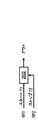
図1は、ヘテロダイン厚さモニタ装置の図であり、化学機械研磨(CMP)装置に使用される従来技術において一般に知られているように、1対の分割周波数の直交に偏光されたビームは、混ぜられてヘテロダインされる前に別個の光学経路で伝達される。従って、ヘテロダイン厚さモニタシステム100は、大まかに、CMP装置、ウェハ110、及び測定光学アセンブリを備えている。ウェハ110は、基板112と膜114とを含む。
FIG. 1 is a diagram of a heterodyne thickness monitor device, as commonly known in the prior art used in chemical mechanical polishing (CMP) devices, a pair of split frequency orthogonally polarized beams is It is transmitted in a separate optical path before being mixed and heterodyned. Accordingly, the heterodyne
測定光学アセンブリは、大まかに、反射されたビームの光周波数におけるドップラーシフトを検出し測定するための様々なコンポーネントを備え、これには、レーザー光源140、ビームスプリッタ(BS)144、偏光ビームスプリッタ(PBS)146、ビームの4分の1波長プレート148、ビーム反射体152、ビームの4分の1波長プレート150、ミックス偏光子143、光電検出器147、ミックス偏光子145、光電検出器149、及び、光電検出器147及び149の出力と電気的に接続された信号処理アセンブリ154が含まれる。
The measurement optics assembly generally comprises various components for detecting and measuring the Doppler shift at the optical frequency of the reflected beam, which includes a
運転中、レーザーダイオード140は、第1の波長の第1の直線偏光成分102と、第1の偏光コンポーネントに直交に偏光する第2の波長の第2の直線偏光成分103とを有するビームを放射する。第1及び第2の偏光成分102及び103は、両方の成分の一部がビーム114及び115としてミックス偏光子145に向かって反射されるBS144に共線的に伝播し、次にビーム116及び117として信号I2が生成される検出器149に反射される。
In operation, the
偏光成分102及び103の透過した一部は、ビーム104及び105としてPBS146に伝播される。PBS146において、成分104は、ビーム106として第1の透過経路を辿り、参照4分の1波長プレート148を通過して反射板152まで至り、4分の1波長板148を通過してビーム122(ビーム106に対して直交に偏光)として後方反射され、PBS146において、ミックス偏光子143に向かい且つビーム124として検出器147の方へ反射する。
The transmitted parts of the
成分105からの第2の偏光成分は、ビーム106として第1のパスから分離した透過経路を辿り、第1の偏光成分104に対して直交に方向付けされ、従って、PBS146から反射し、ビーム109として4分の1波長プレート150を通過し、光学的に透明な回転可能なキャリア115に伝播する。ビーム109は、回転可能なキャリア115の後ろの表面、基板112との間の接触面及び膜114の上面において部分的な反射をし、従って、それぞれ部分的に反射されたビーム111,111T,111Bを生成する。反射されたビーム109S,109T,109Bのそれぞれは、4分の1波長プレート150を通って後方に伝播し、ビーム113S,113T,113BとしてPBS146を透過し、ビーム124,115S,115T,115Bとしてビーム122とともにミックス偏光子145へ共線的に伝播し、次に、信号I2として光電検出器147において検出される。重要なことには、I2は、別の光の周波数で振動し、膜と相互作用するビーム107と、他の光の周波数で振動し、膜と相互作用しない第2の光学経路を伝播するビーム106の両方から生成される。信号I1及びI2は、厚さ寸法を測定するために比較される。
The second polarization component from the
測定ビームが光路長変化を受けると、うなり信号は、図2に描かれたシミュレーション結果に示されるように、対応する位相シフトを経験するであろう。そこでは、表面が研磨によって侵食される場合には、うなり信号I2(プロット103)の位相は、膜114の上面から部分的に反射されたビーム111Tの光路長の変化が原因となって、うなり信号I1(プロット105)からΔφシフトされて描かれる。
When the measurement beam undergoes a path length change, the beat signal will experience a corresponding phase shift, as shown in the simulation results depicted in FIG. There, when the surface is eroded by polishing, the phase of the beat signal I2 (plot 103) is caused by the change in the optical path length of the
図に示すように、測定経路において、ビーム111Bは、ウェハを透過し、ウェハの前の表面から反射される。ウェハを通して光のビーム経路が短縮されるため、ビーム111Bの反射された光の周波数は、ドップラーシフトを受ける。従って、1つの光の周波数(ビーム111,111B及び111T)は、ターゲットと相互作用する一方、第2の光の周波数(ビーム122)は相互作用しない。しかし、そのような方法で参照ビームと測定ビームとを分離することは、ヘテロダイン干渉計のS/N比を低下させ、測定感度を下げてしまうという不利な点を有する。
As shown, in the measurement path, the
一般に、従来技術において知られているヘテロダイン干渉計の分解能は、約6Åに制限され、従って、従来技術に係るヘテロダイン干渉計は、薄膜を正確に測定するのに必要な、又は、処理の間における厚さの小さな変更をモニタするのに必要な分解能を欠く。 In general, the resolution of heterodyne interferometers known in the prior art is limited to about 6 mm, so that prior art heterodyne interferometers are required to accurately measure thin films or during processing. It lacks the resolution necessary to monitor small changes in thickness.
本発明は、非常に正確な位相シフト情報をヘテロダインされた光学的信号から得るためのヘテロダイン反射率計システム及び方法を対象とし、それから正確な厚さを計算することができる。ヘテロダイン反射率計は、大まかに、分割光学的周波数を有する光学的光源と、光学的なうなり信号を生成する一対の光学式のミキサーと、光学的うなり信号を検出して電気的ヘテロダインうなり信号に変換するための一対の光検知器と、2つの電気的信号間の位相シフトを検出するための位相シフト検出器とを備える。 The present invention is directed to a heterodyne reflectometer system and method for obtaining highly accurate phase shift information from a heterodyne optical signal, from which an accurate thickness can be calculated. A heterodyne reflectometer roughly includes an optical light source having a split optical frequency, a pair of optical mixers that generate an optical beat signal, and an optical heterodyne beat signal by detecting the optical beat signal. A pair of photodetectors for conversion and a phase shift detector for detecting a phase shift between two electrical signals are provided.
光源は、それぞれの分離した光周波数、即ち、それぞれω及びω+Δωの分割周波数のp偏光及びs偏光されたビーム成分を有し、互いに直交する直線偏光した2つの成分を含む直線偏光光線を発生させる。2つの周波数を有する直線偏光ビームは、膜の方に向けられて、それと相互作用し、その結果、その成分の膜の中の光路の増加によって、一方の光学的な偏光成分が他方に遅れることとなる。ミックス偏光子は、反射された偏光成分を混ぜる。1つの検出器が膜層から反射されたビームを受け取り、測定信号を発生する。第2検出器は、膜層の上の入射に先立ってビームを受け取り、参照信号を生成する。反射されたビーム成分は、膜との相互作用のため、参照信号に対して位相シフトを有する。 The light source generates a linearly polarized light beam having two linearly polarized components orthogonal to each other, each having a p-polarized and s-polarized beam component at respective separate optical frequencies, ie, split frequencies of ω and ω + Δω, respectively. . A linearly polarized beam having two frequencies is directed towards and interacts with the film, so that an increase in the optical path in the film of that component causes one optical polarization component to lag behind the other. It becomes. The mixed polarizer mixes the reflected polarization components. One detector receives the beam reflected from the film layer and generates a measurement signal. The second detector receives the beam prior to incidence on the film layer and generates a reference signal. The reflected beam component has a phase shift with respect to the reference signal due to interaction with the film.
反射されたビームは、システムの入射角を膜のブルースター角の近傍に設定することによって、膜厚測定のために最適化され、それは、光源波長においてその屈折率によってコントロールされる。参照信号及び測定信号の間の最も大きな位相シフトは、ビームの入射がブルースター角に設定される場合に存在する。測定信号及び参照信号は、位相シフトのために、位相検出器によって分析される。両者間の位相シフトの量は、膜の厚さと関連している。検出された位相シフトは、膜厚の結果のために、厚さ計算機に供給される。一般に、厚さ結果は、より低い厚さほどより正確であり、より高い厚さほどより正確でない。 The reflected beam is optimized for film thickness measurement by setting the incident angle of the system near the Brewster angle of the film, which is controlled by its refractive index at the source wavelength. The largest phase shift between the reference signal and the measurement signal exists when the beam incidence is set to the Brewster angle. The measurement signal and the reference signal are analyzed by a phase detector for phase shifting. The amount of phase shift between the two is related to the thickness of the film. The detected phase shift is fed to the thickness calculator for film thickness results. In general, the thickness results are more accurate for lower thicknesses and less accurate for higher thicknesses.
厚さ結果の精度は、測定信号の中でエラーをキャンセルすることによって大幅に増大され、即ち、測定されたヘテロダイン位相シフトは、予想される位相シフトとは異なり、従って、エラーを含んでいる。エラー補正アルゴリズムは、既知の共通の屈折率及び既知の膜厚を有するテスト膜に対して、ヘテロダイン位相シフトを測定することによって構築される。キャリブレーション膜に対する測定された位相シフトは、同等の厚さのために導かれる予想された位相シフトと比較され、それから測定され予想された位相シフトから定式化される。測定されたヘテロダイン位相シフトは、エラー補正を用いて補正することができる。 The accuracy of the thickness result is greatly increased by canceling the error in the measurement signal, i.e. the measured heterodyne phase shift is different from the expected phase shift and therefore contains errors. The error correction algorithm is constructed by measuring the heterodyne phase shift for a test film having a known common refractive index and a known film thickness. The measured phase shift for the calibration film is compared with the expected phase shift derived for the equivalent thickness and then formulated from the measured and expected phase shift. The measured heterodyne phase shift can be corrected using error correction.
この本発明は、また、組み合わせのヘテロダイン反射率計及び格子干渉計システムと、補正されたヘテロダイン位相シフト情報及び補正された格子位相シフト情報を同時に得るための方法とをも対象とし、それから、非常に正確な厚さが計算され、膜の屈折率が厚さ計算において動的にアップデートされる。これは、上述されたヘテロダイン反射率計システムに格子干渉計を含めることによって実現され得る。 The present invention is also directed to a combined heterodyne reflectometer and grating interferometer system and method for obtaining corrected heterodyne phase shift information and corrected grating phase shift information simultaneously, and The exact thickness is calculated and the refractive index of the film is dynamically updated in the thickness calculation. This can be achieved by including a grating interferometer in the heterodyne reflectometer system described above.
ピッチ“p”を有する格子は、0次及び1次のバンドに反射されたビームを回折させ、それは、別々の検出器によって検出される。検出器は、0次ビームを受け取り、他の測定信号を生成する。もう一方の検出器は、1次のビームを受け取り、格子信号を生成する。上記のように、格子からの測定信号及び参照信号は、位相シフトのために位相検出器によって分析され、それは、膜の正確な屈折率とともに、膜の厚さと関連付けられる。逆に、どちらの測定信号も、格子誘発位相シフトを検出するために、格子信号とともに、位相検出器によって分析され得る。膜の屈折率は、膜の上のビームの波長、格子ピッチ、及び入射角のために、格子位相シフト及びヘテロダイン位相シフトから直接計算される。屈折率及びヘテロダイン位相シフトとともに、膜の厚さは、波長、ピッチ、及び入射角のために決定される。逆に、膜の厚さは、屈折率とは無関係に、且つ屈折率を知ることなく、波長、ピッチ、入射のため、格子位相シフトとヘテロダイン位相シフトから直接計算することができる。しかし、格子信号も補正されるべきエラーを含んでいる。格子エラー補正アルゴリズムは、厚さ又は屈折率のための予想される格子位相シフトに対して、測定された格子位相シフトを補正するために構築される。既知の厚さを有するテスト膜の格子位相シフトを測定し、厚さに関するそれらの測定結果を予想される格子位相シフトと比較することにより、格子位相シフトエラー補正は、測定及び予想位相シフト間で定式化することができる。測定された格子位相シフトは、補正することができる。 A grating with a pitch “p” diffracts the reflected beam into the zeroth and first order bands, which are detected by separate detectors. The detector receives the zero order beam and generates another measurement signal. The other detector receives the primary beam and generates a grating signal. As described above, the measurement and reference signals from the grating are analyzed by a phase detector for phase shifting, which is related to the thickness of the film, along with the exact refractive index of the film. Conversely, either measurement signal can be analyzed by the phase detector along with the grating signal to detect the grating induced phase shift. The refractive index of the film is calculated directly from the grating phase shift and the heterodyne phase shift due to the wavelength, grating pitch, and angle of incidence of the beam on the film. Along with the refractive index and the heterodyne phase shift, the film thickness is determined for wavelength, pitch, and incident angle. Conversely, the film thickness can be calculated directly from the grating phase shift and the heterodyne phase shift for wavelength, pitch, and incidence regardless of the refractive index and without knowing the refractive index. However, the lattice signal also contains an error to be corrected. A grating error correction algorithm is constructed to correct the measured grating phase shift against the expected grating phase shift for thickness or refractive index. By measuring the grating phase shift of a test film having a known thickness and comparing the measurement results for thickness with the expected grating phase shift, the grating phase shift error correction is performed between the measured and expected phase shifts. It can be formulated. The measured grating phase shift can be corrected.
アップデートされた屈折率は、補正されたヘテロダイン位相シフトと補正された格子位相シフトとから導くことができ、それは、ほぼリアルタイムで厚さ補正を動的にアップデートするために用いられる。従って、膜の屈折率が処理の間にドリフトする状況においてさえ、超薄膜の正確な膜厚の結果を入手することができる。 The updated refractive index can be derived from the corrected heterodyne phase shift and the corrected grating phase shift, which is used to dynamically update the thickness correction in near real time. Thus, accurate film thickness results for ultra-thin films can be obtained even in situations where the refractive index of the film drifts during processing.
さらに、本発明は、入射角の膜の表面に戻るように第1のパスから反射されたビームをリダイレクトすることによって、複光路方式モードにおいて動作することができる。 Furthermore, the present invention can operate in a multi-path mode by redirecting the beam reflected from the first pass back to the surface of the film at the angle of incidence.
本発明に特有であると思われる斬新な特徴は、添付された特許請求の範囲に記述される。ただし、本発明自体だけでなく、好ましい使用態様、さらにその目的及び利点は、図示の具体例の以下の詳細な説明を図面と併せて読むと理解することができる。 The novel features believed to be characteristic of the invention are set forth in the appended claims. However, not only the present invention itself but also preferred modes of use, and further objects and advantages thereof, can be understood by reading the following detailed description of the illustrated examples in conjunction with the drawings.
本発明の他の特徴は、添付図面から、そして以下の詳細な説明から明白になるであろう。 Other features of the present invention will become apparent from the accompanying drawings and from the detailed description that follows.
この本発明は、半導体製造の一部である超薄膜の堆積をモニタするのに有用である。それゆえ、デポジッション手段や拡散炉と一体化され得る。さらに、本発明は、サブ10Åから2000Åの膜厚の範囲で薄膜を測定する、可視光線反射率測定の使用を拡張するための、単純且つ効果的な方法を提供する。本発明を用いることにより、大きな平均故障間隔(MTBF)及び非常に簡単な検出スキームを備えた単色の光源を用いて、優れた結果を得ることが可能である。一般に、この厚さ領域への従来技術に係るスペクトル反射率計の拡張は、複雑な遠紫外線(DUV)光源及び反射性又は反射屈折光学を必要とする。また、従来技術に係る反射率計と対比すると、本発明は、数オングストロームの厚さの上層膜の厚さを決定するのに、下の層に関する事前の知識を必要としない。さらに、この発明に基づくセンサーの所有コストは、典型的な従来技術のDUVスペクトル反射率計のそれよりもはるかに低く、また、本発明の方法は、必要となる測定前処理がより少ないものである。本発明の応用及び以下で開示される技術により、表面形状又は広い領域の測定によって誤差が引き起こされることなく、超薄膜上の領域又は点のターゲットの厚さをプロセッサが正確にモニタすることが可能となる。 This invention is useful for monitoring the deposition of ultra-thin films that are part of semiconductor manufacturing. Therefore, it can be integrated with the deposition means and the diffusion furnace. In addition, the present invention provides a simple and effective method for extending the use of visible light reflectometry to measure thin films in the sub-10 to 2000 film thickness range. By using the present invention, it is possible to obtain excellent results using a monochromatic light source with a large mean time between failure (MTBF) and a very simple detection scheme. In general, the extension of prior art spectral reflectometers to this thickness region requires complex deep ultraviolet (DUV) light sources and reflective or catadioptric optics. Also, in contrast to prior art reflectometers, the present invention does not require prior knowledge of the lower layer to determine the thickness of the upper film, which is a few angstroms thick. In addition, the cost of ownership of a sensor according to the invention is much lower than that of a typical prior art DUV spectral reflectometer, and the method of the invention requires less measurement pretreatment. is there. The application of the present invention and the techniques disclosed below allow the processor to accurately monitor the thickness of a target on a region or point on an ultra-thin film without causing errors due to surface shape or large area measurements. It becomes.
マイケルソンのヘテロダイン干渉計において、干渉参照ビームと測定ビームとは僅かな光の周波数差(一般に〜MHzからKHz)を有する。両者間の干渉は、次の方程式によって表される:
![]()
Bは、縞の可視性を表す信号成分
φは、参照ビームと測定ビームとの間の位相差
Δωは、2つの信号の角周波数差
両者間の干渉は、角周波数の差Δωと等しい角周波数を有するうなり信号として観察することができる。
In the Michelson heterodyne interferometer, the interference reference beam and the measurement beam have a slight optical frequency difference (generally ~ MHz to KHz). The interference between the two is represented by the following equation:
![]()
測定ビームが光路長変化(Δd)を受ける場合、うなり信号は、図2に示されたシミュレーションされた結果に例示されるように、対応する位相シフトΔφ=(4π×Δd)/λをするであろう。そこで、測定うなり信号103の位相は、測定ビームの光路長の変化が原因となって参照うなり信号105からΔφシフトされて描かれる。
When the measurement beam undergoes an optical path length change (Δd), the beat signal has a corresponding phase shift Δφ = (4π × Δd) / λ, as illustrated in the simulated results shown in FIG. I will. Therefore, the phase of the measurement beat
以下に提示された発明は、従来技術の欠点に対応して、薄膜測定に対する単純なヘテロダイン反射率測定のアプローチを提供する。このアプローチによって提供される検出感度は、オングストロームのタイプの膜厚の寸法を正確に測定することができるほどである。さらに、単純な正弦波が使用されるので、位相シフトの測定をリアルタイムで実現することができる。本発明のこれら及び他の特徴は、図3Aに示される超薄膜の厚さを測定するためのヘテロダイン反射率計の説明によってより完全に理解されるであろう。 The invention presented below provides a simple heterodyne reflectometry approach to thin film measurement in response to the shortcomings of the prior art. The detection sensitivity provided by this approach is such that an angstrom type film thickness dimension can be accurately measured. Furthermore, since a simple sine wave is used, phase shift measurements can be realized in real time. These and other features of the present invention will be more fully understood by the description of the heterodyne reflectometer for measuring ultrathin film thickness shown in FIG. 3A.
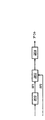
図3Aは、本発明の典型的な具体例に従う、薄膜の厚さを測定するためのヘテロダイン反射率計の図である。本発明のある側面を説明するのに必要であるので、領域301は、図3Bにおけるビームと膜(フィルム)との相互作用の拡大図として議論されるであろう。ヘテロダイン反射率計300は、一般に、膜314及び基板312に入射角αで入射する方向を持った入射ビーム303のための光学を備える。
FIG. 3A is a diagram of a heterodyne reflectometer for measuring thin film thickness according to an exemplary embodiment of the present invention.
ビーム303は、それぞれの分離した光周波数、即ち、それぞれω及びω+Δωの分割周波数のp偏光及びs偏光されたビーム成分を有し、互いに直交する直線偏光した2つの成分を含む。ここに用いられるように、Δωは約20MHzであるが、単なる典型的なものに過ぎず、本発明の範囲を逸脱することなく他の周波数分離が用いられ得る。このビームを発生させるための光源320は、例えばゼーマン分割ヘリウム―ネオンレーザーであり得る。或いは、単一モードレーザー光源からのビームは、例えば音響光学変調器を用い、一方又は両方の別個のビームが所定周波数に周波数シフトした2つの別個のビームに分割することができる。分割周波数のビームは、その後、膜314への入射の前に再結合することができる。光ビームは、当該光ビームの経路の向きを変えるために、任意の適当な光学部品を用い、入射面の中に、そして膜314の方へ方向付けされる。図面に描かれるように、1対の三角形状のプリズム(入射プリズム332及び反射プリズム334)は、膜314に入射する入射ビーム303を方向付けし、膜314から反射されたビーム305を受け入れるが、任意的に、ビームの偏光を保持する間、光路を方向付けするための任意の適当な光学部品でもあり得る。例えば、光源320は、鏡又は他の反射光学部品を用い、入射面(垂線から入射角α)内に方向付けされるか、或いは、所定の入射角でビームを発射するために配置される偏波面保存ファイバに繋げられ得る。
The
ただし、従来技術と著しく対照的に、両方の光周波数の経路が単一の経路に沿って膜と相互作用する、即ち、測定ビームのs偏光成分及びp偏光成分が実質的に同一直線上にあるビームであり、大よそ同軸であることに注目しなければならない。さらに、s偏光及びp偏光の成分から膜314上の照射領域は、ターゲット位置で大よそ同一の広がりを有する。
However, in marked contrast to the prior art, both optical frequency paths interact with the film along a single path, i.e., the s and p polarization components of the measurement beam are substantially collinear. Note that it is a beam, roughly coaxial. Furthermore, the irradiation region on the
本発明のヘテロダイン反射率計の主要な特徴は、測定された位相シフトΔφmから実際の位相シフトΔφを決定することである。測定された位相シフトΔφmは、参照信号Irefの位相と測定信号Ihetの位相との位相差、即ち、反射されなかった経路(参照信号)から得られた信号と反射された経路から得られたうなり信号とのうなりである。真の(又は実際の)位相シフトΔφは、膜層の誤差がない正確な厚さdfを決定するのに必要である。従って、測定された位相シフトΔφmを求めることは、2つの信号検出器を使用するのを必要としており、一つ目は参照信号Irefの検出/生成用であり、二つ目は測定信号Ihetの検出/生成用である。 Major features of the heterodyne reflectometer of the present invention is to determine the actual phase shift [Delta] [phi from measured phase shift [Delta] [phi m. The measured phase shift Δφ m is obtained from the phase difference between the phase of the reference signal I ref and the phase of the measurement signal I het , that is, the signal obtained from the non-reflected path (reference signal) and the reflected path. It is a beat with a beat signal. True (or actual) phase shift Δφ is necessary to determine the exact thickness d f is no error in the film layer. Therefore, determining the measured phase shift Δφ m requires the use of two signal detectors, the first for detecting / generating the reference signal I ref and the second for measuring signal For detection / generation of I het .
信号検出器340は、ミックス偏光子354からの分離したビーム(参照ビーム)304を感知するものであり、ミックス偏光子354は、ビーム304のs及びp偏光成分を膜314から反射する前に混ぜ、ビーム304の位相φを示す参照信号Iref342を生成する。検出器340は、例えばPIN(正―真性―負)検出器、又は、うなり周波数に反応する任意の光検出器であり得る。それは、|ω−(ω+Δω)|のうなり周波数を有する参照信号Irefを発生する。参照信号Iref342は、Δφmが測定された位相シフト検出器362に送信され、そこで、膜314によって引き起こされた測定された位相シフトΔφmを決定するために参照位相として用いられる。
The
一方、信号検出器350は、膜314と相互作用した後にプリズム334から伝播した、ビーム305のs及びp偏光成分を混ぜるミックス偏光子355からの反射ビーム356を感知する。信号検出器350は、測定信号Ihet、352を生成し、それは、ビーム356の位相φ+Δφを示し、参照信号Irefの位相からΔφ位相シフトしている。検出器350は、例として、PIN検出器であり得る。それは、反射光ビーム356をモニタし、ヘテロダイン測定信号Ihetを発生し、Δωのヘテロダイン角周波数をも伴う。測定信号Ihet及び参照信号Irefは、ヘテロダイン位相シフトΔφm(=Δφhet)とともに、図18においてそれぞれ信号プロット1802,1804としてグラフを用いて描かれる。
On the other hand, the
信号352は、測定されたヘテロダイン測定信号Ihet352を参照信号Iref342と比較して測定された位相シフトΔφmを決定するΔφm測定位相シフト検出器362において受信される。位相シフトΔφmは、膜314によって引き起こされ、位相シフトの量は、種々の要因に依る。それには、膜314の厚さ、モニタされる特定の膜に対する、及びより高い位相シフトにおける屈折率nf、補正係数が含まれる。ファクター間の相互関係は、以下で、より大きな特異性において議論されるであろう。どのような場合であっても、正確な膜厚dfは、プロセッサ360によって補正された位相シフトΔφから決定することができ、それは測定された位相シフトΔφmから得られる。しかし、測定された位相シフトΔφmは少なくともより高い位相シフトにおいて、固有誤差を有するので、測定された位相シフトが補正されることによってのみ、正確な厚さ寸法が可能である。
ここで、データ処理システム360が個々の用途によって様々な形式を取り得ることは理解されるべきである。インラインウェハ処理からのデータは、反射率計検出器340及び350又はΔφm測定位相シフト検出器362に電気的に繋げられるコンピュータ又はPCにおいてリアルタイムで処理されることが多い。ただし、他の典型的な具体例に従って、反射率計システムは、リアルタイムでモニタされたデータを格納及び処理するために内部のデータプロセッサ及び/又は個別のファームウェアコンポーネントによって事前設定され得る。まだ他の典型的な具体例に従って、反射率計からの生の測定データは、ウェハプロセス機器内のデータ処理システムによって処理される。その場合、ウェハ処理ファームウェアは、厚さ計算を含め、反射率計の全てのデータ処理を実行する。従って、ヘテロダイン反射率計システム300は、一般的なデータ処理システム360によって描かれ、それは、個別のファームウェア及びハードウェアコンポーネントを含み得る。これらのコンポーネントは、一般に、測定位相シフト補正器366及び厚さ計算機368を含む。任意的に、システム360は、エラー訂正データメモリー364を含み得るものであり、その操作は、以下で議論されるであろう。
Here, it should be understood that the
より具体的には、Δφm位相シフト検出器362は、各検出器から参照信号Iref342及びヘテロダイン測定信号Ihet352を受信し、両者間の位相シフトΔφmを測定する。位相シフト検出器362は、位相検出のために参照信号Iref及び測定信号Ihetの対応点を検出すべく、任意の適当な機構を用いることができる。ただし、これらの改良は、図25及び26A〜26Dに関して別々に議論される。
More specifically, the Δφ m
図には示されないが、位相シフト検出器362は、波長を入力するための入出力インタフェース、及び/又は信号検出を容易にするための発振器周波数情報をも装備することができる。
Although not shown in the figure, the
測定位相シフトΔφmが検出されると、エラー訂正のためにΔφm位相シフト補正器366に渡される。測定位相シフトΔφmのエラーは、より高い位相シフトにおいてかなりであり得るが、エラーは、適切な補正係数の組を多項式関数をΔφmに適用することによって訂正することができる。図7‐図10に対応する以下の議論から明白になるように、補正係数は、個別の膜の屈折率に対して得られる。さらに、エラー訂正計算を実行するために、Δφm訂正器366は、ある種のパラメータデータを必要とする。これらのデータには、光源の波長λ、トップ(一番上)の膜層の屈折率nf、及び入射角αが含まれる。αは、通常はデフォルトのα=60に設定され、光源波長及び膜の屈折率nfに対するブルースター角ちょうどではない。その理由は、以下で議論されるであろう。
When the measured phase shift Δφ m is detected, it is passed to the Δφ m
最終的に、df厚さ計算機368は、Δφm補正器366から補正された位相シフトΔφを受け取り、調査されている膜、即ち膜314に対する補正された膜厚dfを計算する。
Finally, d f thickness calculator 368 receives the phase shift [Delta] [phi which is corrected from [Delta] [phi m corrector 366, a film has been investigated, namely calculating a corrected film thickness d f to the
或いは、df厚さ計算機368は、直接Δφm位相シフト検出器362から測定された位相シフトΔφmを受け取り、メモリー364から取り出す膜厚補正データによって代数的に測定された厚さを補正し得る。厚さエラー補正データ又は検索テーブル(LUT)は、膜314に対する屈折率nfに基づいたメモリー364に予めロードされる。
Alternatively, d f thickness calculator 368 receives the direct [Delta] [phi m
さらに別の選択肢は、個々の測定位相シフト値に対してインデックスが付けられた補正された厚さ値dfのテーブルをメモリー364に記憶することである。その場合、位相シフト検出器362からΔφmを受け取ると、df厚さ計算機368は、メモリー364から補正された厚さ値を取り出し、値を出力する。
Yet another option is to store a table of the individual measured phase shift thickness values were corrected indexed relative value d f in the
今回の方法は、膜の上面からの放射の異方性反射によるものである。従って、ヘテロダイン反射率計の設定は、好ましくは、ブルースター角の近傍の入射角αで設定される。直下に示されるように、膜に対する位相シフトの最大の感度は、検査中の個々の膜の屈折率に対するブルースター角において達成される。ブルースター角において、膜の上面からの反射したp偏光した光の量は、ゼロ又は最小である。従って、検出器350からの信号Ihet352は、膜厚の情報に富むものである。
This method is based on anisotropic reflection of radiation from the upper surface of the film. Accordingly, the setting of the heterodyne reflectometer is preferably set at an incident angle α in the vicinity of the Brewster angle. As shown immediately below, maximum sensitivity of the phase shift to the film is achieved at the Brewster angle relative to the refractive index of the individual film under inspection. At the Brewster angle, the amount of p-polarized light reflected from the top surface of the film is zero or minimal. Therefore, the signal I het 352 from the
ただし、実用的な問題として、モニタシステム中の光学部品は、個々の処理装置と協力するために半恒久的に設定され得る(例えば、予め設定された入射角60°)。そのようなシステムにおいて、精密な角度に入射を調整することは困難又は不可能であり得る。とはいえ、以下の議論において示されるように、ここで説明される発明の1つの利点は、厚さ測定が個々の膜の屈折率に対するブルースター角の周辺の広い角度範囲に亘って非常に正確なことである。 However, as a practical matter, the optical components in the monitor system can be set semi-permanently to cooperate with the individual processing devices (eg, a preset incident angle of 60 °). In such a system, it may be difficult or impossible to adjust the incidence to a precise angle. Nonetheless, as will be shown in the following discussion, one advantage of the invention described here is that the thickness measurement is very large over a wide angular range around the Brewster angle relative to the refractive index of the individual films. It is accurate.
さらに、膜表面からの異方性の反射に加えて、反射の異方性は、膜自体及び底の膜表面又は基板にも存在し得る。膜素材及び下の界面はs及びp偏光のために等方性であるものとされている。ただし、この仮定は、常に全ての膜のタイプに合うものではなく、J. Vac. Sci. Technol. A12(4) 1994年7月/8月の第1152ページに掲載されたティー.ヤスダらの"特異な微斜面のSi−SiO2界面及び水素終端Si表面の光学的異方性"や、J. Vac. Sci. Technol. B3(5) 1985年9月/10月の第1498ページに掲載されたディー.イー.アスプネスの"三次元半導体の上方バンドギャップ光学的異方性:表面の可視‐近紫外線プローブ"を参照されたい。従って、トップの膜及び/又は基板が顕著な反射率異方性を示す状況においては、最適化された入射角は、直角入射とブルースター入射角との間にあり得る。 Furthermore, in addition to anisotropic reflection from the film surface, reflection anisotropy may also be present on the film itself and the bottom film surface or substrate. The membrane material and the underlying interface are assumed to be isotropic due to s and p polarization. However, this assumption does not always suit all film types. J. Vac. Sci. Technol. A12 (4) The tee published on page 1152 of July / August 1994. Yasuda et al., “Optical Anisotropy of Si-SiO 2 Interface and Hydrogen-Terminated Si Surface of Peculiar Slope”, J. Vac. Sci. Technol. B3 (5) 1498, September / October 1985 Dee posted on the page. E. See Aspnes's "Upper bandgap optical anisotropy in 3D semiconductors: surface visible-near UV probes". Thus, in situations where the top film and / or substrate exhibits significant reflectance anisotropy, the optimized angle of incidence can be between normal incidence and Brewster incidence.
より具体的には、膜の次のような領域:a)トップ表面、b)膜の中間、及び/又は、c)底表面の全てにおいて、反射/吸収の異方性が存在し得る。膜の上面において、本質的に、他の偏光の上のブルースター角における一方の偏光の優先的な反射による、上で議論した理由及び論理的根拠によって、フレネル反射が原因となって測定信号の中に位相シフトが引き起こされ得る。一般に、それは殆どの膜にそのまま当てはまり、ノイズに対して大きな信号を与える。しかし、膜表面の上のスクラッチは、反射の異方性に寄与し得、従って、この位相シフトを高める。膜の中間は、特に強磁性の薄膜に関しては、例えばディスクメモリ機器と強誘電性の薄膜、例えばCMOS中のキャパシタについて位相シフトをも引き起こし得る。膜の底の表面(即ち、膜と基板との間の界面)において、結晶方位、又は、強磁性の薄膜に加えて着色結晶格子構造によって位相シフトが引き起こされ得る。 More specifically, reflection / absorption anisotropy may be present in all of the following areas of the film: a) the top surface, b) the middle of the film, and / or c) the bottom surface. On the top surface of the film, essentially due to Fresnel reflections, due to the reason and rationale discussed above, due to the preferential reflection of one polarization at the Brewster angle above the other polarization, A phase shift can be caused in it. In general, it applies directly to most membranes and gives a large signal to noise. However, scratches on the film surface can contribute to the anisotropy of reflection and thus increase this phase shift. The middle of the film can also cause phase shifts, for example for disk memory devices and ferroelectric thin films, eg capacitors in CMOS, especially for ferromagnetic thin films. At the bottom surface of the film (ie, the interface between the film and the substrate), a phase shift can be caused by the crystallographic orientation or colored crystal lattice structure in addition to the ferromagnetic thin film.
例として、SiO2/Si膜の下の界面は、直角入射におけるs及びp偏光の反射のために異方性であると分かっている。SiO2の上面と及び量のバルクメディアが直角入射において等方性であると仮定すると、膜厚に基づいて、測定信号の中に位相シフトが引き起こされ得る。ただし、この場合、シフトは、膜面ではなく、下の界面からの異方性の反射によって引き起こされる。しかし、ここで、ビームは、60°のデフォルト角度ではなく、表面に対して垂直に方向付けされ得る。今回説明された方法は、反射と同様に吸収にも当てはまり、さらに、半導体ウェハの表面などの表面を横切る膜厚のマップを作成するためにウェハを走査するのにも適用可能である。 As an example, the interface below the SiO 2 / Si film has been found to be anisotropic due to the reflection of s and p polarized light at normal incidence. Assuming that the top surface of SiO 2 and the amount of bulk media are isotropic at normal incidence, a phase shift can be induced in the measurement signal based on the film thickness. However, in this case, the shift is caused by anisotropic reflection from the lower interface rather than the film surface. Here, however, the beam can be directed perpendicular to the surface, rather than the default angle of 60 °. The method just described applies to absorption as well as reflection, and is also applicable to scanning a wafer to create a map of film thickness across a surface such as the surface of a semiconductor wafer.
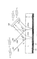
膜面からの異方性の反射についてより一般的なケースに戻り、設定システム300のヘテロダイン反射率計の設定入射角αは、検査中の膜の屈折率nf及び照射光源の波長λと関係し、また、それらとともに変化し得るということが、以下の議論から理解されるであろう。異なる膜は異なる屈折率を有するので、角度αは、インデックスの変化と対応して、調整され得る。必要であれば、ヘテロダイン反射率計システム300の入射角度を調整するために、調査される様々な膜の屈折率に基づく様々な手段が提供される。これは、テーブルシステム310及び/又はプリズム332,334が動くことを可能とすることによって実現され得る。例えば、ミラー332,334は、2度の動きを有して設定され、一つは、ビーム303,305によって形成される入射の面に垂直、且つ、膜314の垂線である軸周りの回転方向にあり、表面法線に平行な並進動作の方向である。或いは、ミラー332,334は、入射面と直角な方向周りに1度の回転運動を有し得るものであり、テーブルアセンブリ310は、垂直な方向に1度の並進動作を有するであろう。後者の典型的な具体例は、動作を表す仮想線によって示されたミラー332,334と、テーブルアセンブリ310(ここでは、テーブル315、膜314、及び基板312として描かれる)とでここに描き出される。仮想の要素は、屈折率nfの値の変化に応じて、異なる入射角αに角度を変えられた入射ビーム303及び受信用の反射ビーム305を示す。ただし、以上や以下で強調されるように、デフォルト入射角α=60°を用いることは、膜及び光源に対するブルースター角で入射角を正確に設定する上で好都合である。
Returning to the more general case for anisotropic reflection from the film surface, the set incident angle α of the heterodyne reflectometer of the
次に図3Bを見ると、膜314に起因する位相シフトΔφの源が描き出される。s偏光成分は、明確さのためにp偏光成分と分離されるものとして描き出される。入射ビーム303は、s偏光成分303s(光の角周波数ωを有する)とp偏光成分303p(光の角周波数ω+Δωを有する)とを含み、それらは互いに直交する。成分303s及び成分303pの両方は、膜314の垂線に対して角度αで入射する。膜314の表面において、ビーム成分303sの一部は、反射光線305‐1s(以下で
![]()
![]()
同様に、ビーム成分303pは、反射光線305−1p(以下で
![]()
![]()
![]()
![]()
Similarly, the
![]()
![]()
膜厚の正確な計算の基本は、膜との光の相互作用を膜厚に対してより敏感になるように最適化することであり、それは、ヘテロダイン位相シフトΔφmを高める。その目的は、参照信号からヘテロダイン信号の位相シフトをできるだけ増大させること、即ち、Δφmを増大させることである。本発明では、これは、等方性の膜及び基板に対する入射角を最適化することによってなされる。反射されたビームが反射され屈折するs及びp成分光線から構成されるので、一方の偏光成分が他方に比べて膜面からの反射光線の大きな部分を有するのが好都合である。分割周波数を有するs及びp偏光された光が測定に用いられるので、この結果を達成するために入射角度αを調整することが可能である。技術的によく理解されているように、直線偏光は、光源波長の入射角をブルースター角に設定することによってこの結果を表すであろう。ブルースター角では、事実上、入射ビーム303pのp偏光成分全体は、305−2pとして膜の中にごく僅かしか屈折されず、もしあったとしても光線として305−1pとして反射される。逆に、ブルースター角において操作すると、入射ビーム303sのs偏光成分は、屈折光線305−2sとして膜を貫く残りの部分とともに、光線305−1sとして顕著な反射が見込まれる。従って、角度αは、1つの偏光成分のより多くが反射されるのではなく膜の中で殆ど全て屈折するように調整され得る。従って、光線が混ぜられた後に、結果として生じるビームは、膜の表面から反射されたs偏光成分の不釣合な寄与によって、位相シフトのために高感度化される。従って、屈折した成分が次式で示される増大した経路距離を移動するのに必要な時間に位相シフトが由来することを理解することができる。
![]()
![]()
等方性の膜及び基板に対して、好ましくは、ビーム303の偏光成分は、直線的且つ互いに直交し、明細書全体に亘ってそのように見なされる。ただし、多少減少するが、楕円偏光した成分も、同様な厚さ誘因位相シフトを生じさせるであろう。従って、本発明の他の典型的な具体例に従って、ビーム303の分割周波数は、楕円偏光する。
For isotropic films and substrates, preferably the polarization components of
本発明の側面によると、偏光された信号をヘテロダインすることの軸外照明アプローチを用いて、非常に敏感な厚さの測定が実現される。反射角がブルースター角の近傍である場合、本発明のこの側面は、膜の上面からの電磁放射の異方性反射に依存する。従来技術の共通又は垂直軸のアプローチにこの方法を利用することの理由は、直下で取り組まれるであろうが、基板が直角入射で顕著な反射率異方性を表す場合には、入射角が直角入射であり得ることが確認されるはずである。 According to an aspect of the invention, a very sensitive thickness measurement is achieved using an off-axis illumination approach of heterodyning the polarized signal. When the reflection angle is in the vicinity of the Brewster angle, this aspect of the invention relies on anisotropic reflection of electromagnetic radiation from the top surface of the film. The reason for using this method for the common or vertical axis approach of the prior art will be addressed directly below, but if the substrate exhibits significant reflectivity anisotropy at normal incidence, the angle of incidence will be It should be confirmed that it can be normal incidence.
単一の積層膜に対するs偏光反射率は、次式で書くことができる:

同様に、p偏光反射率は、次式で与えられる:
![]()
αは、投射角
nは、膜の屈折率
dは、膜厚
Similarly, the p-polarized reflectivity is given by:
![]()
2つの偏光が混じる場合には、検出器によって感知された合成振幅反射率は、次式で書くことができる:
![]()
![]()
パワー反射率は、次式の通りである。:
![]()
reff*は、reffの複素共役
The power reflectivity is as follows: :
![]()
方程式(5)に方程式(2),(3),(4)を代入すると、次式で表すことができる。:
方程式(6)の最初の2項は、s及びpで偏光された光による標準のホモダイン受信法反射率を表している。所与の波長及び膜厚のために、これらの項は、パワー反射率に時不変の(直流の)値を与えている。次の5つの項は、偏光ミキサーでのs及びp偏光光の可干渉性の(コヒーレントな)追加に起因するヘテロダイン反射率を表している。 The first two terms of equation (6) represent the standard homodyne receive method reflectivity with light polarized at s and p. For a given wavelength and film thickness, these terms give a time-invariant (DC) value for power reflectivity. The next five terms represent the heterodyne reflectivity due to the coherent addition of s and p polarized light in the polarization mixer.
位相がtのみによって決定される第3項は、厚さ変化に影響されない。一方では、cos(Δωt±2δ)及びcos(Δωt±4δ)を含む項は、膜厚が変化する際にうなり信号の位相をシフトさせ得る。伝統的なヘテロダイン干渉計測において、測定された位相シフトは、経路の長さ又は厚さの変化と直接比例するであろう。しかし、方程式(6)の非線形な性質のため、測定された位相シフトは、厚さ変化の表れに過ぎず、その直接的な尺度とはならない。 The third term whose phase is determined solely by t is not affected by thickness changes. On the other hand, terms that include cos (Δωt ± 2δ) and cos (Δωt ± 4δ) can shift the phase of the beat signal as the film thickness changes. In traditional heterodyne interferometry, the measured phase shift will be directly proportional to the change in path length or thickness. However, due to the non-linear nature of equation (6), the measured phase shift is only a manifestation of thickness change and is not a direct measure of it.
興味深いことに、+δ及び−δの両方が位相シフトに寄与する。その結果、どのような厚さ変化に対しても直角入射において0位相偏位が起こる。これは、シミュレーション結果によって確認された。これは、直角入射(即ち、従来技術の共通軸の入射)において、cos(Δωt+2δ)の係数がcos(Δωt−2δ)のものと同じであり、cos(Δωt+4δ)の係数がcos(Δωt−4δ)のものと同じであることを実現することによって理解することができる。従って、一方によって引き起こされた位相シフトは、他方によってバランスがとられる。 Interestingly, both + δ and −δ contribute to the phase shift. As a result, zero phase deviation occurs at normal incidence for any thickness change. This was confirmed by simulation results. This is because the coefficient of cos (Δωt + 2δ) is the same as that of cos (Δωt−2δ) and the coefficient of cos (Δωt + 4δ) is cos (Δωt−4δ) at normal incidence (that is, incident on the common axis of the prior art). ) Can be understood by realizing that it is the same. Thus, the phase shift caused by one is balanced by the other.
図4は、直角入射(α=0.0°)において取られたシミュレーション結果の強度対時間のプロットを示す図である。図から、100nmの膜に関する測定信号402のプロットは、参照信号である参照信号プロット404と一致していることが明白であり、即ち、100nmの膜の測定信号及び参照信号が直角入射において同じ位相となっている。また、この結果は測定される膜の厚さによって変わらない。100nmの膜と同じように、50nmの膜に関する測定信号406のプロットも、ローカルな参照プロット404のプロットと同じ位相となっており、即ち、50nmの膜に関する測定信号と参照信号とが直角入射において同じ位相となっていることに気づく。 FIG. 4 shows a plot of intensity versus time for simulation results taken at normal incidence (α = 0.0 °). From the figure it is clear that the plot of the measurement signal 402 for the 100 nm film is consistent with the reference signal plot 404, which is the reference signal, i.e., the 100 nm film measurement signal and the reference signal are at the same phase at normal incidence. It has become. Also, this result does not vary with the thickness of the film being measured. As with the 100 nm film, the plot of the measurement signal 406 for the 50 nm film is also in phase with the plot of the local reference plot 404, ie, the measurement signal and the reference signal for the 50 nm film are at normal incidence. Notice that they are in the same phase.
垂直軸モードと対比すると、軸外モードにおいて、係数(cos(Δωt±2δ)及びcos(Δωt±4δ))の対が異なる。従って、ヘテロダイン反射率計を用いて等方材料における厚さ起因の位相偏位を検出及び測定することが可能である。 In contrast to the vertical axis mode, the pair of coefficients (cos (Δωt ± 2δ) and cos (Δωt ± 4δ)) is different in the off-axis mode. Therefore, it is possible to detect and measure thickness-induced phase deviations in isotropic materials using a heterodyne reflectometer.
図5は、角度20.0°の入射(α=20.0°)において取られたシミュレーション結果の強度対時間のプロットを示す図である。この図から明白なように、100nmの膜に関する測定信号のプロット504は、Δφ(=Δφm)によって参照信号である参照プロット502からシフトした位相である。 FIG. 5 shows a plot of intensity versus time for simulation results taken at an incident angle of 20.0 ° (α = 20.0 °). As is apparent from this figure, the measurement signal plot 504 for the 100 nm film is a phase shifted from the reference plot 502, which is the reference signal, by Δφ (= Δφ m ).
しかし、入射角α=20.0°では、100nmの厚さ変化の位相シフトΔφはかなり小さい。従って、ヘテロダイン反射率計の設定は、リアルタイムの薄膜の厚さ/変化をモニタするのにより有用となるために、厚さにより敏感となるよう最適化されるべきである。 However, at the incident angle α = 20.0 °, the phase shift Δφ of the thickness change of 100 nm is considerably small. Therefore, the heterodyne reflectometer settings should be optimized to be more sensitive to thickness in order to be more useful for monitoring real-time film thickness / change.
入射角がトップの膜に関するブルースター角であるならば、r1pは0に近くなるであろう。換言すると、αがブルースター角となるように入射角を選択することによって、s偏光成分のみが反射されるであろう。p成分の殆どは、膜の中に屈折するであろうし、膜基板界面で反射されるであろう。プラズマエッチング又は堆積のプロセスに関しては、ブルースター角は、arctan(nf/np)で与えられる。ここで、npは、プロセス室の中のガスの屈折率であり、nfは、トップの膜層の屈折率である。その場合、方程式(5)は、次式のように書き換えることができる。:
上記の方程式において、位相情報を有するヘテロダイン項は、r1s(ω)及びr2p(ω+Δω)を含む項のコヒーレントの付加によるものである。これは、古典的なヘテロダイン干渉計に多少類似しており、そして測定ビームから参照ビームを分離することに関係するノイズがない。 In the above equation, the heterodyne term with phase information is due to the coherent addition of terms including r 1s (ω) and r 2p (ω + Δω). This is somewhat similar to a classic heterodyne interferometer and there is no noise associated with separating the reference beam from the measurement beam.
図6は、2つの異なる膜厚に関して角度60°の入射(α=60.0°)において取られたシミュレーション結果の強度対時間のプロットを示す図である。(ここで、多くのブルースター角が57°により近いものであり得るが、当然のことながら、入射角αは60.0°に設定される)。100nmの膜に関する測定信号602のプロット及び50nmの膜に関する測定信号606のプロットの両方は、参照信号であるローカルな参照信号プロット604及び互いからかなり位相シフトしているであるということが図から分かる。図5と比較すると、60°の入射角の観察されたシフトは、20°の入射角よりもかなり大きいことが明らかにされる。(Δωt−δ)を含む項の除去は、技術を厚さ変化により敏感にするように思われる。
FIG. 6 shows a plot of intensity versus time for simulation results taken at an incident angle of 60 ° (α = 60.0 °) for two different film thicknesses. (Here, many Brewster angles can be closer to 57 °, but of course the incident angle α is set to 60.0 °). It can be seen from the figure that both the plot of the measurement signal 602 for the 100 nm film and the plot of the
ヘテロダイン反射率計の設定が厚さにより敏感であるように最適化されると、位相シフトΔφから厚さを決定するための計算を確立することができる。古典的なヘテロダイン干渉計では、位相シフトが測定され、ビームの経路差Δdにおける対応する変化は、以下の式を用いて計算することができる:
![]()
Δdは、対応するビームの経路差
λは、ヘテロダイン照射光源の波長
Once the heterodyne reflectometer setting is optimized to be more sensitive to thickness, a calculation can be established to determine the thickness from the phase shift Δφ. In a classic heterodyne interferometer, the phase shift is measured and the corresponding change in the beam path difference Δd can be calculated using the following equation:
![]()
従って、:
![]()
![]()
ヘテロダイン反射率測定において、Δφ=2δ、及び、
![]()
![]()
方程式(6)を用いるシミュレーションでは、0から100nm(1000Å)までの膜厚に対応するヘテロダイン反射率信号が生成される。そして、各信号の位相シフトΔφは、参照信号を参照して概算される。推定された位相値から、膜厚の対応する値が方程式(10)を用いて予測/計算された。 In the simulation using equation (6), a heterodyne reflectance signal corresponding to a film thickness from 0 to 100 nm (1000 cm) is generated. Then, the phase shift Δφ of each signal is estimated with reference to the reference signal. From the estimated phase value, the corresponding value of the film thickness was predicted / calculated using equation (10).
測定された厚さは、次に、入力された厚さと比較される。測定された厚さと入力された(既知の)厚さとの差は、測定された位相シフトΔφmにおけるエラーの関数である。
dは、測定された位相シフトΔφmから推定される膜厚
nは、膜の屈折率
αは、入射角
λは、ヘテロダイン照射光源の波長
The measured thickness is then compared to the input thickness. The difference between the measured thickness and the input (known) thickness is a function of the error in the measured phase shift Δφ m .
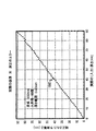
図7は、60°入射角の、推定の膜厚と実際の膜厚との比較の図である。比較プロット702から、約300Åまでの膜厚は、予測された厚さが入力された厚さとうまく合致しており、プロット702が比較的直線的であることが分かる。300Åの厚さを超えると、予測された値におけるエラーは、直線的でない比率で厚さとともに増大する。図8において、薄膜の実際の及び測定された厚さの間のエラー量を描くエラープロット802によって、エラー対入力された厚さが描かれる。
FIG. 7 is a comparison of the estimated film thickness and the actual film thickness at a 60 ° incident angle. From the
図6及び図7から、300Åまでのエラーの量が0又は無視できるが、それを超えるとエラーが急速に増大することが分かる。そうではあるが、このエラーは定量化することができ、エラー計算は、その除去のために公式化することができる。エラーを相殺する1つのメカニズムは、より高次の多項式関数を誤差曲線802に適合させることである。測定された位相シフトΔφm及び実際の位相シフトΔφから計算される、実際の膜厚及び推定の厚さから引き出された多項式関数の係数を用いることにより、厚さ計算におけるエラーを決定することができる。そして、厚さ計算(即ち、測定された位相シフトΔφmを補正すること)において多項式のエラー関数を単に含めることにより、膜厚(即ち実際の膜厚)の予測値を得ることができる。或いは、位相シフト寸法から得られる推定の厚さ値は、厚さエラー補正値を直接推定の厚さに代数的に追加することによって補正することができる。
From FIGS. 6 and 7, it can be seen that the amount of error up to 300 Å is zero or negligible, but beyond that the error increases rapidly. Nevertheless, this error can be quantified and the error calculation can be formulated for its removal. One mechanism to cancel the error is to fit a higher order polynomial function to the
図9及び図10は、60°の入射角に対する膜厚を計算するためのエラー計算の妥当性を証明する。曲線902は、632nmのレーザーに関し、エラー補正後の推定の厚さの結果が700Åまで極めて正確であり、900のÅ範囲まで大変良いことを示す。推定の厚さ値は、900Åの厚さを超えて初めてエラー補正が破綻する。図10の曲線1002から、404nmのレーザーに対するエラー補正結果は、632nmのレーザーを用いた測定の900Åの厚さの障壁を超えてなお正確なままであることが分かる。
9 and 10 demonstrate the validity of the error calculation for calculating the film thickness for an incident angle of 60 °.
上の議論から、トップの膜層の屈折率nfが既知である場合には、膜厚に対する最も正確な結果が得られることは明白である。以上で示されたシミュレーション結果から、適切に設定されたヘテロダイン反射率計は、サブ200nmの領域での膜厚を決定するのに極めて有益であることが証明されている。正確な厚さ結果は、位相シフトから計算された厚さに対するエラー補正を決定することによって、300Åより大きい膜厚において達成することができる。本発明の1つの典型的な具体例に従って、厚さ/位相シフトのエラー補正は、予め決定される。所定の補正とともに、膜厚のその後の元の位置でのモニタにより、ウェハ処理の間、リアルタイムで且つ正確な厚さが実現され得る。 From the above discussion, it is clear that the most accurate results for film thickness are obtained when the refractive index n f of the top film layer is known. From the simulation results shown above, an appropriately set heterodyne reflectometer has proven to be extremely useful in determining film thickness in the sub-200 nm region. Accurate thickness results can be achieved at film thicknesses greater than 300 mm by determining error correction for the thickness calculated from the phase shift. In accordance with one exemplary embodiment of the present invention, the thickness / phase shift error correction is predetermined. With a predetermined correction, a subsequent in-situ monitoring of the film thickness can achieve a real-time and accurate thickness during wafer processing.
図11は、本発明の典型的な具体例に従う、ヘテロダイン位相シフトの大きさを測定するのに用られる位相シフト補正多項式関数の係数を決定する方法を描くフローチャートである。この方法は、1つの既知の屈折率nf及び複数の既知の厚さdfk1-j(ステップ1102)を有する多くのキャリブレーションウェハを選択することから始まる。屈折率は共通のファクターであるので、厚さエラー補正多項式関数の係数は、指数に固有になるであろう。各キャリブレーションウェハの屈折率は、正確な厚さ計算結果を保証するため、生産工程中の上層膜のインデックスと同一であるべきである。一般に、単一の層のNIST追跡可能な酸化物ウェハは、この目的のために様々な屈折率及び膜厚において利用可能であるが、既知の膜厚及び共通の既知の屈折率を有する任意のウェハで十分であろう。典型的なウェハエッチ又は堆積処理のために、選択されたキャリブレーションウェハの膜厚は、5Å刻みで10Åから100Åに及ぶ。 FIG. 11 is a flowchart depicting a method for determining the coefficients of a phase shift correction polynomial function used to measure the magnitude of a heterodyne phase shift, in accordance with an exemplary embodiment of the present invention. The method begins by selecting a number of calibration wafers having one known refractive index n f and a plurality of known thicknesses d fk1-j (step 1102). Since refractive index is a common factor, the coefficients of the thickness error correction polynomial function will be exponential. The refractive index of each calibration wafer should be the same as the index of the upper film during the production process in order to ensure accurate thickness calculation results. In general, single layer NIST trackable oxide wafers are available for this purpose in a variety of refractive indices and thicknesses, but any film having a known thickness and a common known refractive index. A wafer will suffice. For typical wafer etch or deposition processes, the thickness of the selected calibration wafer ranges from 10 to 100 mm in 5 mm increments.
次に、入射角αは、キャリブレーション膜の既知の屈折率nf及び照射光源の波長に基づいて、ヘテロダイン反射率計システムのために調整される(ステップ1104)。好ましくは、入射角は、膜の屈折率のために、可能な限りブルースター角の近傍とされる。しかし、一部のモニタシステムは、設定可能ではない場合もあるが、α=60°等のデフォルト入射角に予め設定され、従って、ブルースター角に入射を調整することは不可能である。そうは言っても、商業的に入手可能な膜の多くがそのデフォルト入射角α=60°(一般に、60°に僅かに満たない)の数度以内にブルースター角を有することが分かっている。システムの多くがデフォルト角度に予め設定されるので、信号ノイズによるいかなる付加的なエラーも無視することができる。その結果、膜に関する精密なブルースター角ではなく、所定のデフォルト、例えばα=60°において多項式の関数に対する係数を導くことが好都合であり得る。その際、係数は、α=60°のデフォルト入射角を有する予め設定されたシステムに適切であるそれらの設定可能なシステムは、膜のブルースター角より僅かに高いのではあるが、60°のデフォルト値に調整された入射角のみを有することができる。入射が膜のブルースター角から数度ずれていることに起因する厚さ測定エラーよりも、入射角度を間違って調整しているか、又は、入射角に対する不適当な多項式関数を用いていることに起因する厚さ測定エラーの方が実質的により大きなエラーであることを理解されているべきである。 Next, the incident angle α is adjusted for the heterodyne reflectometer system based on the known refractive index n f of the calibration film and the wavelength of the illumination source (step 1104). Preferably, the incident angle is as close to the Brewster angle as possible due to the refractive index of the film. However, some monitor systems may not be configurable, but are preset to a default incident angle, such as α = 60 °, and therefore cannot adjust the incidence to the Brewster angle. That said, many commercially available films have been found to have a Brewster angle within a few degrees of their default angle of incidence α = 60 ° (typically less than 60 °). . Since many of the systems are preset to the default angle, any additional error due to signal noise can be ignored. As a result, it may be advantageous to derive the coefficients for the polynomial function at a given default, eg, α = 60 °, rather than the exact Brewster angle for the membrane. In doing so, those configurable systems whose coefficients are appropriate for pre-set systems with a default incident angle of α = 60 ° are slightly higher than the Brewster angle of the membrane, although 60 ° It can only have an incident angle adjusted to a default value. Incorrectly adjusting the incident angle or using an inappropriate polynomial function for the incident angle rather than a thickness measurement error due to the incident being off a few degrees from the Brewster angle of the film It should be understood that the resulting thickness measurement error is substantially larger.
運転中、分割周波数偏光ビームは、ヘテロダイン反射率計システム中の膜から反射され、その結果、各jウェハに対するヘテロダイン測定信号Ihet及び参照信号Irefが生成される(ステップ1106)。測定信号は、参照信号から膜厚に関連する量シフトした位相になるであろう。測定された位相シフトΔφm1-jは、参照信号Irefの位相と各jキャリブレーションウェハに対する測定信号Ihetの位相とから検出される(ステップ1108)。測定された位相シフト情報によって、6次多項式関数の係数を決定することができ、それは、既知の厚さdkf1-jに対しての、そして既知の屈折率nfに対しての、測定された位相シフトΔφm1-jから得られた推定の厚さにおけるエラーに関係する(ステップ1110)。これは、位相差アルゴリズム、例えば方程式(11)を用い、ウェハの既知の厚さdkf1-j及び既知の屈折率nfから実際のΔφを求めることによって実現され得る。続いて、6次多項式関数は、Δφmに内在するエラーを補正し、従って、補正された膜厚を求めるために、測定された位相シフトに適用され得る。 In operation, the split frequency polarized beam is reflected from the film in the heterodyne reflectometer system, resulting in a heterodyne measurement signal I het and a reference signal I ref for each j-wafer (step 1106). The measurement signal will be phase shifted from the reference signal by an amount related to the film thickness. The measured phase shift Δφ m1-j is detected from the phase of the reference signal I ref and the phase of the measurement signal I het for each j calibration wafer (step 1108). With the measured phase shift information, a coefficient of a sixth order polynomial function can be determined, which is measured for a known thickness d kf1-j and for a known refractive index n f . Related to the error in the estimated thickness obtained from the phase shift Δφ m1-j (step 1110). This can be achieved by using the phase difference algorithm, eg, equation (11), to determine the actual Δφ from the known thickness d kf1-j and the known refractive index n f of the wafer. Subsequently, a sixth order polynomial function can be applied to the measured phase shift to correct the error inherent in Δφ m and thus determine the corrected film thickness.
本質的に、エラー補正多項式関数は、正確な膜厚を求めるために、少なくとも3つの方法のうちの1つにおいて用いることができる。第一に、多項式関数は、直接データ処理システムにロードされ、測定された位相シフトΔφmから予測される厚さをエラー補正するために厚さ計算とともに、直ちに実行することができる。或いは、多項式関数は、予め厚さエラー補正のセットを生成するために、厚さ計算とともに用いることができ、それらは、テーブルの中に蓄積され、個々の測定された位相シフトΔφmの値と関連付けられる。任意的に、エラーの訂正された厚さのデータセットは、厚さエラー訂正の代わりに多項式関数と厚さ計算によって作成され、個々の測定された位相シフトΔφm値に対して表の中でインデックスをも付され得る。厚さエラー訂正のテーブルが編集されるならば、動作の間、データプロセッサは、測定された位相シフトΔφmから測定された厚さdmを計算し、それから、テーブルから適切な厚さエラー訂正によってΔφmのエラーを訂正する。或いは、エラーが訂正された厚さデータが用いられるならば、信号のために得られた各測定位相シフトΔφmの表からのエラーが訂正された厚さ測定結果に単にアクセスするに過ぎず、従って、厚さ計算を実行するためのデータプロセッサの必要性がなくなる。 In essence, the error correction polynomial function can be used in one of at least three ways to determine the exact film thickness. First, the polynomial function is loaded directly into the data processing system and can be immediately performed with a thickness calculation to error-correct the predicted thickness from the measured phase shift Δφ m . Alternatively, a polynomial function can be used with the thickness calculation to generate a set of thickness error corrections in advance, which are stored in a table and the values of the individual measured phase shifts Δφ m and Associated. Optionally, an error-corrected thickness data set is generated by a polynomial function and thickness calculation instead of thickness error correction, and in the table for each measured phase shift Δφ m value. It can also be indexed. If the thickness of the error correction table is edited during operation, the data processor, the thickness d m measured from the measured phase shift [Delta] [phi m is calculated and then, the appropriate thickness error correction from the table To correct the error of Δφ m . Alternatively, if error-corrected thickness data is used, the error from the table of each measured phase shift Δφ m obtained for the signal is simply accessed, and the thickness measurement results are simply accessed. Thus, the need for a data processor to perform the thickness calculation is eliminated.
ここで、1つの物理的な機械で引き出した補正係数が別の装置に上手く翻訳し得ず、即ち、その二つが同一に設定されているとしても、エラー補正精度がある程度劣り得ることもまた理解されるべきである。換言すると、位相シフトエラー補正多項式のために引き出された係数は、少なくとも部分的に装置特有のものであり得る。従って、理想的に、Δφmは、膜厚を測定するのに用いられる同じ装置から取得されるべきである。それにもかかわらず、特定の生産器具に対する一連の係数の妥当性は、一連の検査ウェハの膜厚を測定することによって確認され得るものであり、各立証ウェハは、共通の屈折率、及び、モニタされる膜の範囲内の既知の膜厚を有する膜を備える。検査ウェハの屈折率は、モニタされる膜のそれに類似している。 Here, it is also understood that the correction coefficient extracted by one physical machine cannot be translated well into another device, that is, even if the two are set the same, the error correction accuracy can be somewhat inferior. It should be. In other words, the coefficients derived for the phase shift error correction polynomial may be at least partially device specific. Therefore, ideally, Δφ m should be obtained from the same device used to measure film thickness. Nevertheless, the validity of a set of coefficients for a particular production instrument can be verified by measuring the film thickness of a set of inspection wafers, each verified wafer having a common index of refraction and a monitor. A film having a known film thickness within the range of the film to be formed. The refractive index of the inspection wafer is similar to that of the film being monitored.
プロセスは、生産運転を開始するのに先立って6次多項式関数をデータプロセッサのRAMメモリーに読み込むことで終わり、それは、各測定Δφmに対するリアルタイムの補正されたΔφを求めるための膜厚計算において実行され、そこからエラー補正された厚さが生成される(ステップ1112)。或いは、6次多項式関数は、将来使用するために記憶され得る。エラー補正された厚さの結果のために導かれた一連の係数の精度が屈折率nf、及び、キャリブレーションウェハを測定するのに用いられるセットアップパラータ(即ち、光源波長λ及び入射角α)に依存しているため、インデックス情報は、各補正係数とともに保持されるべきである。 The process ends by reading a 6th order polynomial function into the RAM memory of the data processor prior to starting the production run, which is performed in the film thickness calculation to determine the real time corrected Δφ for each measurement Δφ m From there, an error-corrected thickness is generated (step 1112). Alternatively, the sixth order polynomial function can be stored for future use. The accuracy of the series of coefficients derived for the error-corrected thickness result is the refractive index n f and the setup parameters used to measure the calibration wafer (ie, source wavelength λ and incident angle α). Index information should be kept with each correction factor.
任意的に、厚さエラー補正又はエラー補正された厚さのどちらかを有するLUTは、直ちに使用するために、メモリーに直接保存されるか又はロードされる(ステップ1112)。エラー補正多項式と同様に、参照屈折率及び設定パラメータは、LUTとともに保存されるべきである。 Optionally, LUTs having either thickness error correction or error corrected thickness are stored or loaded directly into memory for immediate use (step 1112). As with the error correction polynomial, the reference refractive index and setting parameters should be stored with the LUT.
直前で言及されたように、多くの場合、ヘテロダインモニタ装置は設定可能ではないであろうことが予想される。その場合、屈折率及び個々の装置に予め設定される設定パラメータに基づいて、適切な多項式関数が識別される必要がある。多くのモニタシステムが通例の値、即ち、α=60°及びλ=404nm又は632nmに予め設定されることが予想されるが、他のものもまたあり得る。これを受けて、通例でない設定パラメータ値にふさわしい利用可能な複数の補正係数はそれらのシステムのヘテロダイン反射率測定膜厚測定プロセスの適用性を実質的に増大させるであろうということが理解されるであろう。従って、代わりの典型的な具体例に関しては、多項式関数に対する複数の組の補正係数が、設定可能なモニタシステムを用いて、個々の屈折率に対して、及び、例えば波長及び入射角などの様々な設定パラメータ値に対して予め導かれ得る。これは、図11のフローチャートに描かれたキャリブレーションプロセスを通して繰返すこと、及び、膜に関するブルースター角以外の角度にαをリセットすることによって実現され得る(ステップ1104参照)。多項式関数のための個々の設定された補正係数は、各屈折率について、設定パラメータ値の各組み合わせのために求められ得る。個々の生産器具のための一連の係数の妥当性は、生産運転を開始するのに先立って、一連の検査ウェハの既知の厚さを測定/確認することによって、個々の物理的な装置の使用のために確認されなければならない。同様な方法の中で、一連の補正係数は、異なる波長を有する光源を用いるキャリブレーションプロセスを通して繰返すことによって、様々な光源波長のために導かれ得る。従って、現在説明された発明は、厚さ測定において精度を犠牲にせずに様々なシステム構成に適応し得る。 As mentioned immediately above, it is expected that in many cases the heterodyne monitoring device will not be configurable. In that case, an appropriate polynomial function needs to be identified based on the refractive index and the preset parameters preset for the individual device. Many monitoring systems are expected to be preset to the usual values, ie α = 60 ° and λ = 404 nm or 632 nm, but others are also possible. In view of this, it is understood that a plurality of available correction factors suitable for unusual setting parameter values will substantially increase the applicability of the heterodyne reflectometry film thickness measurement process of those systems. Will. Thus, for an alternative exemplary embodiment, multiple sets of correction factors for the polynomial function can be set for individual indices of refraction using a configurable monitoring system and various, eg, wavelength and angle of incidence. Can be derived in advance for various setting parameter values. This can be achieved by repeating through the calibration process depicted in the flowchart of FIG. 11 and resetting α to an angle other than the Brewster angle for the film (see step 1104). An individual set correction factor for the polynomial function may be determined for each combination of set parameter values for each refractive index. The validity of a series of coefficients for an individual production instrument is determined by the use of individual physical equipment by measuring / verifying the known thickness of a series of inspection wafers prior to starting a production run. Must be confirmed for. In a similar manner, a series of correction factors can be derived for various light source wavelengths by repeating through a calibration process using light sources having different wavelengths. Thus, the presently described invention can be adapted to various system configurations without sacrificing accuracy in thickness measurement.
本発明は、エラー補正厚さ方程式を用いることにより、直ちに非常に正確な膜厚の計算をすることを容易にする。上で簡潔に議論されるように、本発明に関する1つの極めて有益な応用は、ウェハエッチング又は堆積の工程などの間にリアルタイムの膜厚の結果を得るためのものである。 The present invention facilitates a very accurate calculation of the film thickness immediately by using the error correction thickness equation. As briefly discussed above, one very beneficial application for the present invention is for obtaining real-time film thickness results, such as during a wafer etch or deposition process.
図12A及び図12Bは、本発明の典型的な具体例に従う、ヘテロダイン反射率計の信号から非常に正確な膜厚測定を得るためのプロセスのフローチャートである。プロセスは、例えば生産ウェハのようなウェハのトップの膜層に対する初期の屈折率nfを決定することから始まる(ステップ1202)。次に、膜の屈折率nfにふさわしい6次多項式関数に対する一連の係数が識別され、該関数はシステムRAMにロードされる(ステップ1204)。システムが所定の入射角に予め設定されるならば、システム入射角度を調整することができないので、一連の補正係数も、参照された入射角に基づいて選択されなければならない。 12A and 12B are flowcharts of a process for obtaining a very accurate film thickness measurement from a heterodyne reflectometer signal, in accordance with an exemplary embodiment of the present invention. The process begins by determining an initial refractive index n f for the top film layer of the wafer, such as a production wafer (step 1202). Next, a set of coefficients for a 6th order polynomial function appropriate for the refractive index n f of the film is identified and loaded into the system RAM (step 1204). Since the system incident angle cannot be adjusted if the system is preset to a predetermined incident angle, a series of correction factors must also be selected based on the referenced incident angle.
多項式関数は、測定された位相シフトΔφmにおけるエラーを補正するために用いられ、一度補正されると、正確な膜厚dfを計算するために用いることができる。しかし、得られるエラー補正された膜厚dfは、一般に上で議論された2つの基本的な手続:多項式関数を用いて補正された膜厚を直ちに決定すること;又は、検索テーブルに対する厚さエラー補正又は補正された厚さ値を予め計算すること、のうちの1つによって決定されることができる。厚さエラー補正は、測定された位相シフトΔφmから得られた測定された厚さ値、dmを補正するのに用いられる。或いは、補正された厚さ値は、測定された位相シフトに基づいてテーブルの中で単に探され得る。後者のケースのどちらかにおいて、膜の屈折率nfにふさわしい補正データを有するLUTがシステムメモリーにロードされる(ステップ1204)。ヘテロダイン反射率計モニタシステムが設定可能であると仮定すれば、それは、関数によって参照された設定パラメータ(即ち、光源波長λ及び入射角α)に基づいて、再設定される(ステップ1206)。 Polynomial function is used to correct errors in the measured phase shift [Delta] [phi m, and once corrected, it can be used to calculate the exact thickness d f. However, the error corrected thickness d f obtained generally discussed above the two basic procedures: it immediately determine a corrected film thickness using a polynomial function; or thickness to the search table of It can be determined by one of error correction or pre-calculating the corrected thickness value. The thickness error correction, the measured measured thickness value obtained from the phase shift [Delta] [phi m, used to correct the d m. Alternatively, the corrected thickness value can simply be looked up in a table based on the measured phase shift. In either of the latter cases, an LUT having correction data appropriate for the refractive index n f of the film is loaded into system memory (step 1204). Assuming that the heterodyne reflectometer monitor system is configurable, it is reset (step 1206) based on the configuration parameters referenced by the function (ie, source wavelength λ and incident angle α).
典型的な生産工程が、適合する膜の屈折率をそれぞれ有する、多くのプロセスウェハから構成されるであろうし、従って、前述のステップを典型的な生産工程におけるその後のウェハに対して繰り返す必要がないことが予想される。次に、厚さ寸法を進めることができる。 A typical production process will consist of many process wafers, each with a matching film refractive index, and thus the above steps need to be repeated for subsequent wafers in a typical production process. Not expected. The thickness dimension can then be advanced.
ウェハは、反射率計のテーブルに搭載され、図3Aの説明について上で説明されたビームが照射される(ステップ1208)。膜層からの反射された参照及び測定のビームがそれぞれ検出され、参照信号Iref及び測定されたヘテロダイン信号Ihetに変換される。信号Ihet及びIrefは、(測定された位相シフト)Δφm検出器において受け取られ(ステップ1212)、Δφm検出器は、信号の位相から測定された位相シフトΔφmを決定する(ステップ1210)。次に、Δφmは、補正係数とともに多項式関数を用い、エラーに関して補正される(ステップ1214)。補正された位相シフトΔφとともに、補正された膜厚dfは、方程式(10)などの標準の厚さ計算を用いて決定され(ステップ1218)、例えば末端のアルゴリズムにおいて使用するために出力することができる。 The wafer is mounted on a reflectometer table and irradiated with the beam described above for the description of FIG. 3A (step 1208). Reflected reference and measurement beams from the membrane layer are detected and converted into a reference signal I ref and a measured heterodyne signal I het , respectively. Signal I het and I ref are received at (measured phase shift) [Delta] [phi m detector (step 1212), [Delta] [phi m detector determines the phase shift [Delta] [phi m measured from the signal of the phase (step 1210 ). Next, Δφ m is corrected for errors using a polynomial function with a correction factor (step 1214). With corrected phase shift [Delta] [phi, corrected film thickness d f is the equation (10) is determined using standard thickness calculations, such as (step 1218), for example, be output for use at the end of the algorithm Can do.
ステップ1204に関して言及されるように、ステップ1212に戻り、測定された位相シフトΔφmは、代わりに厚さ計算に用いられ得るが、エラーは、結果である測定された厚さdfmまで遂行されるであろう。この厚さエラーは、厚さエラー補正をdfmに適用することによって取り除くことができる(ステップ1216)。その場合、厚さエラー補正データセットは、メモリーの中にロードされるであろうし、必要に応じて取り出された個々の厚さ補正値は、測定された位相シフトΔφmに基づいているであろうし、補正された膜厚dfが出力される(ステップ1218)。さらに交互に、一連のエラー補正された厚さデータは、メモリーにロードされ得る。それは、個々の測定された位相シフトに基づく厚さ値のためにアクセスされる。従って、厚さデータが測定された位相シフト値に前処理され、インデックスを付されるであろうため、厚さ計算が実行される必要はない。 As mentioned with respect to step 1204, returning to step 1212, the measured phase shift Δφ m can be used instead in the thickness calculation, but the error is performed up to the resulting measured thickness d fm. It will be. This thickness error can be removed by applying a thickness error correction to d fm (step 1216). In that case, the thickness error correction data set will be loaded into memory and the individual thickness correction values retrieved as needed will be based on the measured phase shift Δφ m. Roshi, corrected film thickness d f is output (step 1218). Alternately, a series of error-corrected thickness data can be loaded into memory. It is accessed for thickness values based on individual measured phase shifts. Therefore, no thickness calculation needs to be performed since the thickness data will be preprocessed and indexed to the measured phase shift value.
プロセスが停止しないと仮定すれば、全ての厚さ寸法がウェハに対して完了するまで(ステップ1220)、フローはステップ1210から繰返す。完了すると、別のウェハに対するチェックがなされ得る(ステップ1222)。他のウェハが処理されないには、プロセスが終了し、そうでなければ、新しいウェハ上の膜の屈折率が前のウェハの屈折率と照合される(ステップ1224)。2つが一致するならば、新しいウェハが反射率計テーブルの上に搭載されることによりプロセスが開始され(ステップ1208)、そこから継続される。インデックスが変わらないので、補正多項式又はシステム設定のどちらをも意図されない。しかし、新しいウェハからの屈折率及び前のウェハが一致しないならば、補正係数の現在の組は適切でなく、異なる補正多項式関数が選択される。反射率計システムが設定可能ならば、反射率計システムは、新しい屈折率のために再設定されるべきである。従って、プロセスがステップ1202から再度開始する。どちらの場合にも、最終的な厚さ測定結果が運転中の最後のウェハから取られるまで、上で説明されるように、測定のプロセスが続く。そして、プロセスが終了する。
Assuming that the process does not stop, the flow repeats from
以上の議論は、単一の層、主に薄膜の応用に重点を置いたものである。しかし、以下で示されるであろうように、エラーの変化は、複数のスタックに拡張され得る。しかし、最初に、より複雑なスタックには2つのレーザー波長が必要となり得ることが前提とされ、その結果、興味のある厚さの隔たりに対する厚さを正確に評価するために、2つの別個の厚さ補正が必要である。サブ2000Åの膜厚のモニタに対するテスト結果が以下に示される。 The above discussion focuses on the application of a single layer, mainly thin films. However, as will be shown below, the error change can be extended to multiple stacks. Initially, however, it is assumed that more complex stacks may require two laser wavelengths, so that two separate wavelengths are needed to accurately assess the thickness for the thickness separation of interest. Thickness correction is required. Test results for a sub 2000 mm film thickness monitor are shown below.
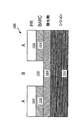
図13は、出願人によってテスト体制において精査されたものに類似する、溝掘りされた複数層のスタックの図である。構造1300は、概略的に、フォトレジスト(PR)層1314、底の非反射コーティング(BARC)層1316、酸化被膜1318、及びシリコン基板1312を備える。シミュレーションの目的で、構造1300は、2つの領域A及びBに分割される。領域Bは、チャンネル1320がPR層1314及びBARC層1316を横切っており、従って、酸化被膜1318の表面を露呈する構造1300の一部を表している。領域Aは、PR層1314の表面が露出する構造1300の一部である。両方の領域の振幅反射率は、特有のマトリクス法を用いて計算され得る。現在のヘテロダイン反射率計が空間でコヒーレントなビームを用いるので、これらの反射率は、構造1300の反射率を計算するためにコヒーレントに加算される。PR層1314の厚さはほぼ0から2000Åまで変化される一方、他の2つの層の厚さは一定に維持される。領域AのPR層1314の厚さが変更されると、領域Bの溝1320の深さが対応して変更される。
FIG. 13 is a diagram of a sliced multi-layer stack similar to that scrutinized by the applicant in a test regime. The
上述のように、一般に、選択された各波長のブルースター角に対応する入射角を用いると、興味の厚さ間隔を評価するのに2つのレーザー波長(λ)ヘテロダイン反射率計が必要であろうということが予測される。採用されるレーザー光線の光源は、632nm及び404nmの波長を有する。興味の厚さ間隔に対する最適な波長を慎重に選択することによって、うなり信号の位相シフトから上層膜の厚さを正確に予測することができる。図14A‐14Dは、0‐2000Åの厚さ間隔に亘って、入力された厚さの関数として予測される厚さのプロットを描く図である。図から収集されるように、入射角をトップの膜層のブルースター角に設定し、厚さ間隔0Å‐900Å及び1600Å‐2000Åは、λ=632nmを有する光源を用いて正確に予測することができるが、910Å‐1590Åの範囲の厚さは正確に予測できなかった。その厚さ間隔に対して、満足な厚さ測定精度を実現するために、λ=404nmを有する光源が採用された(図14C参照)。 As noted above, in general, using an incident angle corresponding to the Brewster angle of each selected wavelength, two laser wavelength (λ) heterodyne reflectometers are required to evaluate the thickness spacing of interest. It is predicted that it will be. The laser light source employed has wavelengths of 632 nm and 404 nm. By carefully selecting the optimal wavelength for the thickness interval of interest, the thickness of the overlayer can be accurately predicted from the phase shift of the beat signal. 14A-14D depict plots of predicted thickness as a function of input thickness over a thickness interval of 0-2000 mm. As collected from the figure, the incident angle is set to the Brewster angle of the top film layer, and the thickness spacings 0Å-900Å and 1600Å-2000Å can be accurately predicted using a light source with λ = 632 nm. Although possible, thicknesses in the range of 910 to 1590 were not accurately predicted. In order to achieve satisfactory thickness measurement accuracy for the thickness interval, a light source having λ = 404 nm was employed (see FIG. 14C).
従って、入射角としてブルースター角を用いる状態で、溝を有する多重積層構造の厚さを正確に予測するのに2つの波長が必要であり得ることを理解することができる。2つの別個のエラー補正解決策には2つの固有な波長が必要であり、正確に厚さを予測するためには、4組の多項式の係数が必要である。しかし、さらなるコンピュータ実験により、単一のレーザー波長、即ち632nmのみを用いて、0Å‐2000Åの全体の厚さの範囲が予測できた角度に入射がセットされたことが証明された。テストされた膜試料に対し、その入射角は、632nmの波長を有する光の源を用いて、60°と実験的に決定された(ここで、トップの膜層のブルースター角は、光源波長に対する57.38°である)。従って、たった2組の多項式の係数のみを有し、たった1組のアルゴリズムのみが必要である。予測された厚さと0Å‐2000Åに亘る厚さの隔たりの間の入力された厚さとの比較の結果が図15A及び図15Bに示される。従って、本発明の典型的な具体例に従って、入射角αは、60°と予め定められ、よって、2つの波長のテロダイン反射率計を設定することの必要性がなくなる。 Therefore, it can be understood that two wavelengths may be required to accurately predict the thickness of a multi-layer structure with grooves, using the Brewster angle as the angle of incidence. Two distinct error correction solutions require two unique wavelengths and four sets of polynomial coefficients are needed to accurately predict thickness. However, further computer experiments have shown that using only a single laser wavelength, i.e. 632 nm, the incidence was set at an angle where the entire thickness range of 0Å-2000Å could be predicted. For the tested film samples, the incident angle was experimentally determined to be 60 ° using a light source having a wavelength of 632 nm (where the Brewster angle of the top film layer is the source wavelength) To 57.38 °). Thus, only two sets of polynomial coefficients are needed, and only one set of algorithms is required. The results of a comparison of the predicted thickness with the input thickness between the thickness gaps ranging from 0 to 2000 mm are shown in FIGS. 15A and 15B. Thus, in accordance with a typical embodiment of the present invention, the angle of incidence α is predetermined as 60 °, thus eliminating the need to set up a two wavelength terodyne reflectometer.
今回説明された発明は、ヘテロダインされた反射率計を用いて超薄膜の厚さをリアルタイムで正確に決定するための、単純なメカニズム及び方法を提供する。しかし、関連した技術において理解されるように、古典的な厚さ計算は、ターゲット材の屈折率に関する正確な値を有することに高く依存している。工程が進むと、上層膜の屈折率がしばしばドリフトするか又は変化し、従って、さらなるエラーが厚さ計算に入ってくるので、このことは、半導体ウェハ処理の間に正確な厚さを実現するのに問題となる。 The presently described invention provides a simple mechanism and method for accurately determining the thickness of ultrathin films in real time using a heterodyned reflectometer. However, as will be appreciated in the related art, classical thickness calculations are highly dependent on having an accurate value for the refractive index of the target material. As the process progresses, the index of refraction of the top layer often drifts or changes, thus further errors come into the thickness calculation, which achieves an accurate thickness during semiconductor wafer processing. It becomes a problem.
本発明の別の典型的な具体例に従って、ヘテロダイン反射率計は、薄膜の厚さ及び屈折率を同時に決定するための格子干渉計と連携する。さらに、厚さ計算は、格子干渉計からの情報を用いて得られた屈折率を用い、リアルタイムで動的にアップデートされる。本発明のこれらの及び他の側面は、以下で議論されるシステム及び方法の説明から理解されるであろう。 In accordance with another exemplary embodiment of the present invention, the heterodyne reflectometer works in conjunction with a grating interferometer for simultaneously determining thin film thickness and refractive index. Furthermore, the thickness calculation is dynamically updated in real time using the refractive index obtained using information from the grating interferometer. These and other aspects of the invention will be understood from the system and method descriptions discussed below.
図16は、本発明の典型的な具体例に従って、膜の屈折率のために動的にアップデートされた値を用い、エラー補正された膜厚を得るための、組み合わせのヘテロダイン反射率計及び格子干渉計の図である。ヘテロダイン反射率計/格子干渉計システム1600(HR/GI1600)は、多くの側面において、図3Aについて上で議論されたヘテロダイン反射率計システム300と類似しているので、2つの具体例の差異のみが詳細に議論されるであろう。図面から明白な1つの特徴は、HR/GI1600が、検出器1611を有するヘテロダイン反射率計サブセクション(小区分)1670と、0次ビーム検出器1612及び1次ビーム検出器1623を有する格子干渉計サブセクション1680とにさらに細かく分かれていることである。ヘテロダイン反射率計サブセクション1670は、上述したのと同一に機能し、検出器1611が測定信号Ihetを発生し検出器1610が参照信号Irefを発生する(信号1620及び342と信号1621及び352と同様に、検出器1610及び1611は検出器340及び350と相互に関連がある)。測定信号Ihet及び参照信号Irefは、ヘテロダイン位相シフトΔφhetとともに、図18において、信号プロット1802及び1804としてそれぞれ描かれる。上述したように、測定されたヘテロダイン位相シフトΔφmは、Δφm検出器362によって検出されるが、明瞭さのために、測定された格子位相シフトΔφgrtmとして“Δφhetm”と称され、同様に議論されるであろう。
FIG. 16 illustrates a combined heterodyne reflectometer and grating to obtain error-corrected film thickness using dynamically updated values for the film refractive index in accordance with an exemplary embodiment of the present invention. It is a figure of an interferometer. Since the heterodyne reflectometer / grating interferometer system 1600 (HR / GI 1600) is similar in many aspects to the
一方、格子干渉計サブセクション1680は、格子1630を利用し、格子1630は、複数の回折バンドの中にビーム1640が回折するためのピッチ“p”を有し、1次の光線1643のみが用いられるいくつかのより高次(1次、2次、3次等の回折バンド)が明るい中心のバンド(ゼロ次光線1642)の両側に並ぶ。格子のピッチは、本質的に、3つの要件:選択された波長λに対するブラッグ回折条件、厚さ測定のためのダイナミックレンジ、及び、格子干渉計分解能を満たすことに基づく。簡単に図17A及び図17Bを見ると、格子1630に関する作用の原理が分かり、そこから、回折した光ビームの少なくとも一部が参照信号から追加量、即ち、2つの別個の位相シフト分シフトした位相になるであろうということが理解できる。s偏光成分は、明瞭さのために、これらの図において、p偏光成分と区別して描かれる。上述したように、最初の位相シフトは、膜314との相互作用に起因する。入射ビーム303は、反射光線305−1sと、屈折光線305−2s及び305−2pとに分離し、屈折光線及び反射光線のそれぞれが互いに垂直距離x分離した状態で基板によって反射される。ここで、:
dfは、膜厚
ρは、膜の屈折率
αは、入射角
nfは、膜の屈折率
On the other hand, the
第2の位相シフトは、格子回折1630からの回折光バンド、光線1643のみで起こり、その結果、1次の回折バンド(回折波1643−1s、1643−2s、及び1643−2p)のみで観察される。そこで、回折格子1630によって発生する1次の光線、光線1643−1s、1643−2s、及び1643−2pは、コヒーレント加算で、格子誘発位相シフトδgrtを表し、次のように定義される経路差PDと対応している:
mは、回折バンドの整数定数であり、1次バンドに対してはm=1
λは、ヘテロダイン照射光源の波長
ρは、膜の屈折率
The second phase shift occurs only in the diffracted light band from grating
λ is the wavelength of the heterodyne irradiation light source ρ is the refractive index of the film
ゼロ番目バンドビーム1642は、回折しないが、格子回折1630を通して直接変化しないパスであるため、格子1630との相互作用からの格子誘発位相シフトδgrtは、1次光線1643−1s、1643−2s、及び1643−2pのみで見られる(入射角度αがブルースター角の近傍で選択されるので(デフォルトの入射角α=60°)、r1p(ω+Δω)≒0であるので、反射光線305−1p、即ち、BS1632の後の1640−1pはないことを思い出されたい)。上述のように、膜に起因する位相シフトは、光線305−2s及び305−2pの2δhetである。従って、1次の屈折光線1643−2s及び1643−2pの格子における全体の位相シフトδGIは、2δGIであり、ここで、δGI=δhet+δgrt。である。
Since the
図16に戻って、格子干渉計サブセクション1680は、0次回折ビーム及び1次回折ビームに対する2つの別個の信号をそれぞれ作り出すために、検出器1612及び1613を利用する。格子1630からの0次光線1642が回折しないので、それらの位相は、格子1630によって変化しない。従って、検出器1612は、ヘテロダイン測定信号Ihet1622を発生させ、測定信号Ihetに対する位相シフトは、検出器1610からの参照信号Irefに対して、本質的にΔφhetのままである。従って、実際問題として、パス356及び検出器1611は、BS1632と同様に、割愛することができる。
Returning to FIG. 16, the
逆に、格子1630からの1次光線1643は回折し、フーリエシフト定理に従って、格子δgrtからの追加の位相シフトが生じることとなる。検出器1613は、1次ビーム1643から格子信号IGI1623を発生させる。測定された格子位相シフトΔφGImは、信号Ihet及びIrefからΔφhetmを検出するのと同一の方法によって、信号Ihet及びIGIから検出することができる。信号Ihet及びIref間の測定された位相シフトΔφhetmは、上述されたように、膜の光学的厚さについての情報を提供する。信号IGI及びIhetの間の格子位相シフトΔφgrtmは、一方では、膜の屈折率nfを決定するのに有益な追加の情報を提供する。従って、信号Iref、Ihet、及びIGIから膜の屈折率nfを得ることが可能である。
Conversely, the
Δφhetm検出器362は、参照信号Iref1620、及び、測定信号Ihet1621又は1622のいずれかを各検出器から受け取り、両者の間の位相シフトΔφhetmを検出/測定する。上の他の場所で議論されるように、測定された位相シフトΔφhetmは、例えば多項式関数を用いて厚さ計算をするのに先立ってエラー補正されるべきである。従って、Δφhet補正器366は、Δφhetm検出器362から測定された位相シフト値Δφhetmを受け取り、エラー補正アルゴリズムを適用する。補正された位相シフトΔφhetは、次に、df計算機368に渡されるが、直下で議論される理由のために、nf計算機1696にも渡される。
The Δφ hetm detector 362 receives the
Δφgrtm検出器1690は、格子信号IGI1623、及び、各検出器からの測定信号Ihet1621又は1622のいずれかを受け取り、格子のみによって格子信号IGI1623で誘発された位相シフトを検出/測定し、即ち、Δφgrtmは、格子信号IGI1623、及び、測定信号Ihet1621又は1622のいずれかとの間で検出される。測定信号Ihet及び格子信号IGIは、図19において、ヘテロダイン位相シフトΔφgrtとともに、それぞれ信号プロット1802及び1902として描かれる。
The Δφ grtm detector 1690 receives the
本発明の1つの特徴は、リアルタイムでアップデートされ補正された膜の屈折率の値によって、動的に厚さ計算をアップデートする能力である。従って、製造工程の中で、極めて正確な膜厚を達成可能であり、それは、膜のリフラクタンスの変化と無関係である。屈折率の変化は、プロセス自体からの屈折率nfの変化、例えば、ゲートプロセスにおいてハイ‐ケー(高誘電率)SiONを形成するSiO2の窒化物形成が原因となり得る。 One feature of the present invention is the ability to dynamically update thickness calculations with real-time updated and corrected film refractive index values. Thus, very accurate film thicknesses can be achieved during the manufacturing process, which is independent of changes in the film refractance. The change in refractive index may be due to a change in the refractive index n f from the process itself, for example, nitridation of SiO 2 which forms a high-ke SiON in the gate process.
検査されている膜の屈折率は、位相シフトΔφhet及び位相シフトΔφgrtから決定することができる。しかし、測定されたヘテロダイン位相シフトΔφhetmと同様に、Δφgrtm検出器1690によって検出された測定された格子位相シフトΔφgrtmは、指数計算に先立って補正しなければならない潜在エラーを有する。補正された格子位相シフトΔφgrtは、次に、nf計算機1696に送られる。nf計算機1696は、nfを決定するために(以下の方程式(24)などの)別個の関数を利用し、次に、df計算機368に送られる。膜厚計算、例えばdf計算機368によって使用された上の方程式(10)は、膜厚dfの計算のためにnfを利用する。 The refractive index of the film being inspected can be determined from the phase shift Δφ het and the phase shift Δφ grt . However, similar to the measured heterodyne phase shift Δφ hetm , the measured grating phase shift Δφ grtm detected by the Δφ grtm detector 1690 has a potential error that must be corrected prior to the exponent calculation. The corrected grating phase shift Δφ grt is then sent to the n f calculator 1696. n f calculator 1696 utilizes a separate function (such as the following equation (24)) in order to determine the n f, then sent to the d f calculator 368. Thickness calculation, for example, d f equation above used by the computer 368 (10) utilizes n f for the calculation of the film thickness d f.
或いは、膜厚dfは、実際の補正された格子位相シフトΔφgrt及び補正されたヘテロダイン位相シフトΔφhetから直接求められ得る。そこで、位相シフトΔφgrtは、Δφgrt補正器1692から受け取られ、Δφhetは、df計算機370としてΔφhet補正器366から受け取られる。膜厚計算、例えばdf計算機370によって上で使用された方程式(23)は、nfとは無関係な膜厚dfを計算する。 Alternatively, the film thickness d f can be determined directly from the actual corrected grating phase shift [Delta] [phi grt and corrected heterodyne phase shift [Delta] [phi het. Therefore, the phase shift [Delta] [phi grt is received from [Delta] [phi grt corrector 1692, [Delta] [phi het is received from [Delta] [phi het corrector 366 as d f calculator 370. Thickness calculation, for example, have been used above by d f calculator 370 Equation (23), and n f calculates unrelated thickness d f.
セットアップは、ブルースター角の近傍の入射角α(α=60°)を有するように設定される。この角度では、膜の上面からのp偏光した光線の反射は、ごく僅かであるか、又は全くない。それによって、検出器1611からの測定信号Ihet1621を膜厚情報が豊かなものとすることができる。Si基板の上の薄膜のために、検出器1611からの測定信号Ihetは、次式で表現することができる。:
![]()
![]()
方程式(14)において、位相情報のヘテロダイン項は、r1s(ω)及びr2p(ω+Δω)に関係する項のコヒーレント加算による。方程式(18)からの膜厚情報の抽出は、他の場所において説明される。 In equation (14), the heterodyne term in the phase information is due to coherent addition of terms related to r 1s (ω) and r 2p (ω + Δω). Extraction of film thickness information from equation (18) is described elsewhere.
格子干渉計の目的は、膜の位相/厚さの測定の代替アプローチを提供することである。この測定結果をヘテロダイン反射率計からのものと組み合わせることによって、膜の屈折率を決定することができる。ヘテロダイン反射率計の分析に続いて、格子干渉計からの1次のビームのために次の方程式が理解され得る。1つの膜スタックのために、s偏光反射率は、次の方程式によって表すことができる。
方程式としてのp偏光反射率:
2つの偏光が混じる場合、検出器によって感知された結果の振幅反射率は、次のように書くことができる:
従って、パワー反射率は、次のように表現できることになる。
方程式(18)において、方程式(15)、(16)、及び(17)を代入した後、検出器1613におけるブルースター角のRGIからの信号IGI1623は、次のように表現することができる:
方程式(14)は、検出器1611又は1612からの測定信号Ihetを表している。格子干渉計1680では、測定信号1622Ihet及び格子信号1623IGIの0交差をモニタすることによって、格子誘発位相シフトδgrtを決定することができる。格子誘発位相シフトδgrtは、他の周知の位相測定技術によっても検出することができる。
Equation (14) represents the measurement signal I het from the
参照信号1620Irefと測定信号1621又は1622Ihetトの0交差を比較することによって、超薄膜によって引き起こされた位相シフトΔφhetを決定することができる。ヘテロダイン位相シフトΔφhetは、他の周知の位相測定技術によっても検出することができる。このヘテロダイン位相シフトは、次のように表すことができる。
測定信号1621又は1622Ihet及び格子信号1623IGIから、格子誘発位相シフトΔφgrtは、Δφhetとは無関係に決定され得る。格子位相シフトは、次のように表すことができる。
方程式(22)を方程式(21)と掛け合わせ、その後に簡単な代数によって、物理的な厚さは、次のように表すことができる。
方程式(21)を方程式(22)割り、その後に簡単な代数によって、屈折率nは、次のように表すことができる。
従って、図16に計算機370で示されるように、格子干渉測定(GI)と連携する今回のヘテロダイン反射率測定(HR)は、薄膜の物理的な厚さdf、及び屈折率nfの両方を独立して決定するために用いることができ、計算機370は、計算機368によって導かれるdfアウトプット369とは無関係にdfアウトプット371を導く。この特徴は、膜が厚さの変化と同時に指数変化を受ける場合に、ゲート誘電体計測学の中で特に重要である。例えば、ハイケーのゲート酸化物プロセスの間に、誘電体膜は、光学的な厚さ変化を受ける。この変化の一部は、膜の膨らみや、いくぶんその指数変化に原因がある。この二つを分離できることは、工程管理にとって重要である。従来技術の手法では、それらが測定するパラメータから互いに独立な2つの変化に完全に解析することができない。膜厚df及び膜の屈折率nfの両方が、ヘテロダイン位相シフトΔφhetとは無関係に判断することができる格子誘発位相シフトΔφgrtを用い、無関係に判断することができるので、今回のプロセスは、この欠点を克服する。
Accordingly, as shown in FIG. 16 by
屈折率計算は、正確な格子位相シフト情報Δφgrtと同様に正確なヘテロダイン位相シフト情報Δφhetを必要としており、従って、補正アルゴリズムは、それぞれの測定値を補正するために導かれる。ヘテロダイン位相シフト補正アルゴリズムを既知の膜厚と既知の回折インデックスを用いてキャリブレーションウェハから求めるプロセスは、図11に示されたフローチャートに関して上述されている。格子位相シフト補正アルゴリズムを既知の膜厚とピッチpを有する格子の既知の回折指数を用いてキャリブレーションウェハから導くプロセスは、位相シフト補正アルゴリズムを求めるための同時進行プロセスとして図20に描かれる。 The refractive index calculation requires accurate heterodyne phase shift information Δφ het as well as accurate grating phase shift information Δφ grt, and therefore a correction algorithm is derived to correct each measurement. The process of obtaining a heterodyne phase shift correction algorithm from a calibration wafer using a known film thickness and a known diffraction index is described above with respect to the flowchart shown in FIG. The process of deriving a grating phase shift correction algorithm from a calibration wafer using a known diffraction index of a grating having a known film thickness and pitch p is depicted in FIG. 20 as a concurrent process for determining a phase shift correction algorithm.
従って、プロセスは、1つの既知の屈折率nfと複数の既知の厚さdfk1-jとを有する多くのキャリブレーションウェハを選択することから始まる(ステップ2002)。ヘテロダイン反射率計システムは、可能ならば、キャリブレーション膜及びヘテロダイン光源波長の既知の屈折率nfkに基づいて、入射角αを調整される(ステップ2004)。或いは、入射角αは、所定のデフォルト値α=60°にセットされている場合もある。この時点で、格子のピッチpにも注目される。 Thus, the process begins by selecting a number of calibration wafers having a known refractive index n f and a plurality of known thicknesses d fk1-j (step 2002). The heterodyne reflectometer system adjusts the incident angle α, if possible, based on the known refractive index n fk of the calibration film and the heterodyne source wavelength (step 2004). Alternatively, the incident angle α may be set to a predetermined default value α = 60 °. At this point, attention is also paid to the pitch p of the lattice.
操作中、分割周波数の偏光ビームは、ヘテロダイン反射率計システムの膜から反射され、その結果、各jウェハに対してヘテロダイン測定信号Ihet及び格子信号IGIが生じる(ステップ2006)。これらの信号は、測定されたヘテロダイン位相シフトΔφhetmの多項式関数用の補正係数のセット、及び、測定された格子位相シフトΔφgrtmの多項式関数用の補正係数の別のセットを決定するために、キャリブレーションウェハの既知の膜厚パラメータとともに用いられる。測定されたヘテロダイン位相シフトΔφhetmは、各jキャリブレーションウェハの参照信号Iref及び測定信号Ihetから検出され(ステップ2008)、次に、測定された位相シフトm1-jのエラーに関係する6次多項式関数用の係数の決定に用いられる(ステップ2010)。同様な方法で、測定された格子位相シフトΔφgrtmは、各jキャリブレーションウェハの測定信号Ihet及び格子信号IGIから検出される(ステップ2012)。そして、実際の格子位相シフトΔφgrtk1-jは、(上の方程式(22)に例示するように)既知の膜厚dfk1-jと複数の既知の屈折率nfとから計算することができ、それは、測定された位相シフトΔφgrtm1-jのエラーと関係する6次多項式関数用の係数のセットを導くために用いられる(ステップ2014)。重要なことには、補正された格子位相シフトΔφgrt及び補正されたヘテロダイン位相シフトΔφhetは、(例えば、上の方程式(24)用いて)膜の屈折率nfを求めるのに用いられるであろう。膜厚計算は、補正された位相シフトから屈折率nfとともに動的にアップデートすることができる。従って、測定されたヘテロダイン位相シフトΔφhetmを有する補正係数のセット、及び、測定された格子位相シフトΔφGImを補正するための多項式関数を有する補正係数の第2のセットは、キャリブレーションウェハ及び設定パラメータの参照屈折率とともに保存される。 In operation, the split frequency polarized beam is reflected from the film of the heterodyne reflectometer system, resulting in a heterodyne measurement signal I het and a grating signal I GI for each j wafer (step 2006). These signals are used to determine a set of correction factors for the polynomial function of the measured heterodyne phase shift Δφ hetm and another set of correction factors for the polynomial function of the measured grating phase shift Δφ grtm Used with known film thickness parameters of the calibration wafer. The measured heterodyne phase shift Δφ hetm is detected from the reference signal I ref and measurement signal I het of each j calibration wafer (step 2008), and then relates to the error of the measured phase shift m1-j 6. It is used to determine the coefficient for the second order polynomial function (step 2010). In a similar manner, the measured grating phase shift Δφ grtm is detected from the measurement signal I het and grating signal I GI of each j calibration wafer (step 2012). The actual grating phase shift Δφ grtk1-j can then be calculated from the known film thickness d fk1-j and the plurality of known refractive indices n f (as illustrated in equation (22) above). , It is used to derive a set of coefficients for a 6th order polynomial function associated with the measured phase shift Δφ grtm1-j error (step 2014). Importantly, the corrected grating phase shift Δφ grt and the corrected heterodyne phase shift Δφ het can be used to determine the refractive index n f of the film (eg, using equation (24) above). I will. The film thickness calculation can be updated dynamically with the refractive index n f from the corrected phase shift. Accordingly, the set of correction factors having a measured heterodyne phase shift Δφ hetm and the second set of correction factors having a polynomial function for correcting the measured grating phase shift Δφ GIm are the calibration wafer and settings Stored with the reference refractive index of the parameter.
本発明は、エラー補正厚さ方程式を用いて、膜厚を直ちに非常に正確に計算するのを容易にし、それは、膜層の屈折率の変化に対して動的にアップデートされる。従って、ウェハ処理の間の屈折率の変化は、膜厚の結果の精度に影響しないであろう。厚さ計算の間にインデックスを動的にアップデートするための1つの典型的な方法が以下に存在する。 The present invention uses an error-correcting thickness equation to facilitate the immediate and very accurate calculation of the film thickness, which is dynamically updated with changes in the refractive index of the film layer. Thus, refractive index changes during wafer processing will not affect the accuracy of the film thickness results. One exemplary method for dynamically updating the index during thickness calculation exists below.
図21A及び図21Bは、ヘテロダイン反射率計信号から補正された膜厚を得るためのプロセスのフローチャートであり、厚さ計算の屈折率成分が本発明の典型的な具体例に従って動的にアップデートされる。プロセスは、ウェハ、例えば生産ウェハのトップの膜層の入射の屈折率nfを決定することから始まる(ステップ2102)。インデックスを用い、2つの適切な多項式関数が、測定された信号の中でエラーを補正するためにインデントされ、システムRAMにロードされる(ステップ2104)。最初の多項式関数は、補正係数の適切なセットによって、測定されたヘテロダイン位相シフトΔφhetmにおいてエラーを補正するために識別される。第2の多項式関数は、補正係数の適切なセットによって、測定された格子位相シフトΔφgrtmにおいてエラーを補正するために識別される。測定されたヘテロダイン位相シフトΔφhetmの多項式関数のためのヘテロダイン補正係数は、測定されたヘテロダイン位相シフトΔφhetmから補正されたヘテロダイン位相シフトΔφhetを決定するために用いられ、そしてそれは、正確な膜厚を生成するために用いることができる。逆に、測定された格子位相シフトエラーの多項式関数のための格子補正係数は、測定された格子位相シフトΔφgrtmから補正された格子位相シフトΔφgrtを決定するために用いられ、そしてそれは、膜の正確な屈折率nfを生成するために補正されたヘテロダイン位相シフトΔφhetと連携して用いることができる。厚さ計算の精度が屈折率の精度に依存しているので、この新しい屈折率は、膜厚計算(例えば厚さ方程式(10))の屈折率項を動的にアップデートするために用いられる(ステップ2106)。個々のプロセスウェハの膜の屈折率が通常一定のままであるので、このステップが典型的な生産工程では、それ以降のウェハに対して繰り返される必要はない。厚さ測定計算は、動的にアップデートされた屈折率によって、ここから進むことができる。 FIGS. 21A and 21B are flowcharts of a process for obtaining a corrected film thickness from a heterodyne reflectometer signal, where the refractive index component of the thickness calculation is dynamically updated according to an exemplary embodiment of the present invention. The The process begins with determining an incident refractive index n f of a top film layer of a wafer, eg, a production wafer (step 2102). Using the index, two appropriate polynomial functions are indented to correct errors in the measured signal and loaded into the system RAM (step 2104). The first polynomial function is identified to correct the error in the measured heterodyne phase shift Δφ hetm by an appropriate set of correction factors. The second polynomial function is identified to correct the error in the measured grating phase shift Δφ grtm by an appropriate set of correction factors. Heterodyne correction coefficients for the polynomial function of the measured heterodyne phase shift [Delta] [phi Hetm is used to determine the heterodyne phase shift [Delta] [phi het corrected from the measured heterodyne phase shift [Delta] [phi Hetm, and it is accurate film Can be used to generate thickness. Conversely, the grating correction factor for the polynomial function of the measured grating phase shift error is used to determine the corrected grating phase shift Δφ grt from the measured grating phase shift Δφ grtm , and Can be used in conjunction with a corrected heterodyne phase shift Δφ het to produce an accurate refractive index n f of Since the accuracy of the thickness calculation depends on the accuracy of the refractive index, this new refractive index is used to dynamically update the refractive index term in the film thickness calculation (eg, the thickness equation (10)) ( Step 2106). This step need not be repeated for subsequent wafers in a typical production process, since the refractive index of the film of an individual process wafer usually remains constant. Thickness measurement calculations can proceed from here with dynamically updated refractive indices.
ウェハは、反射率計テーブル(ステップ2108)に搭載され、照射される。光源からの参照ビームと膜層からの測定及び格子ビームが検出され、参照信号Iref、測定されたヘテロダイン信号Ihet、及び格子信号IGIに変換される。ヘテロダイン測定信号Ihet及び参照信号IrefがΔφhetmヘテロダイン位相シフト検出器で受け取られ、同時に、ヘテロダイン測定信号Ihet及び格子信号IGIが格子誘発位相シフト検出器格子Δφgrtmで受け取られる(ステップ2110)。Δφhetm検出器は、Iref及びIhet信号からΔφhetmを決定する(ステップ2112)。 The wafer is mounted on the reflectometer table (step 2108) and irradiated. The reference beam from the light source and the measurement and grating beam from the film layer are detected and converted into a reference signal I ref , a measured heterodyne signal I het , and a grating signal I GI . The heterodyne measurement signal I het and the reference signal I ref are received at the Δφ hetm heterodyne phase shift detector, and at the same time the heterodyne measurement signal I het and the grating signal I GI are received at the grating induced phase shift detector grating Δφ grtm (step 2110). ). The Δφ hetm detector determines Δφ hetm from the I ref and I het signals (step 2112).
測定されたヘテロダイン位相シフトΔφhetmは、Δφhetmのエラー補正多項式関数を用い、実際のΔφhetに補正される(ステップ2114)。測定されたヘテロダイン位相シフトΔφhetmをエラー補正することは、従来技術の方法論の厚さ測定の精度を大いに高めるが、さらには、処理の間、変化又はドリフトする膜厚計算におけるパラメータを動的にアップデートすることによってより一層の正確さを達成することが可能である;最も重要なものは、膜の屈折率である。従って、並列動作において、Δφgrtm検出器は、Ihet及びIGI信号からΔφgrtmを決定する(ステップ2116)。そして、測定された格子位相シフトΔφgrtmは、Δφgrtmに対するエラー補正多項式関数を用いて、実際のΔφgrtに補正される(ステップ2118)。 The measured heterodyne phase shift Δφ hetm is corrected to the actual Δφ het using an error correction polynomial function of Δφ hetm (step 2114). While error correction of the measured heterodyne phase shift Δφ hetm greatly increases the accuracy of thickness measurements in prior art methodologies, it also dynamically adjusts parameters in thickness calculations that change or drift during processing. It is possible to achieve even greater accuracy by updating; the most important is the refractive index of the film. Thus, in parallel operation, the Δφ grtm detector determines Δφ grtm from the I het and I GI signals (step 2116). The measured grating phase shift Δφ grtm is corrected to an actual Δφ grt using an error correction polynomial function for Δφ grtm (step 2118).
実際の補正された格子位相シフトΔφgrt及び補正されたヘテロダイン位相シフトΔφhetを有することによって、屈折率のプロセス値は、(ソース波長情報λ、入射角α、及びピッチpなどの他の必要な情報とともに、)屈折率計算、例えば方程式(22)を用いて決定することができる(ステップ2120))。そして、アップデートされた屈折率nfは、リアルタイムの膜厚計算において、屈折率パラメータを動的にアップデートするのに用いることができ(ステップ2120)、そこから(当然ながらソース波長情報λ及び入射角αを用いて)膜厚dfが得られる(ステップ2124)。例えば末端決定において用いられるために、dfが出力され得る(ステップ2126)。 By having the actual corrected grating phase shift Δφ grt and the corrected heterodyne phase shift Δφ het , the process value of the index of refraction (other required values such as source wavelength information λ, incident angle α, and pitch p) Along with the information, it can be determined using a refractive index calculation, eg, equation (22) (step 2120)). The updated refractive index n f can then be used to dynamically update the refractive index parameter in the real-time film thickness calculation (step 2120), from there (of course the source wavelength information λ and the incident angle). using alpha) thickness d f is obtained (step 2124). For example, in order to be used in the terminal decision, d f it can be output (step 2126).
代わりに又は同時に、ステップ2118において、(ソース波長情報λと入射角αとともに)上の方程式23を用い、実際の補正された格子位相シフトΔφgrt及び補正されたヘテロダイン位相シフトΔφhetから直接膜厚dfが得られ得る(ステップ2123)。そして、格子干渉計サブシステムから導かれたdfの値は、ヘテロダイン反射率計サブシステムから導かれ、品質保証確認検査として及び/又は直接例えば末端決定において用いられ、dfの値と比較することができる(ステップ2126)。
Alternatively or simultaneously, in
フローは、プロセスが停止する(ステップ2128)まで、現在のウェハに対してステップ2110から継続的に繰り返し、その間、別のウェハが入射屈折率(ステップ2130及び2132)のために調査される場合もあり、最終的な厚さ測定が運転における最後のウェハから行われるまで、上述のような測定プロセスが続く。そして、プロセスが終了する。
The flow will continue to repeat from
本発明のさらに別の典型的な具体例に従って、測定信号Ihetは、反射されたビームを入射角で膜ターゲットに戻るようにリダイレクトする(向きを変える)ことによって強められる。この複光路方式アプローチは、上述の単光路アプローチの膜面からのp偏光された光線の優れた抑制の利点を有している。 In accordance with yet another exemplary embodiment of the present invention, the measurement signal I het is enhanced by redirecting the reflected beam back to the membrane target at an angle of incidence. This double path approach has the advantage of excellent suppression of p-polarized light from the film plane of the single path approach described above.
図22は、本発明の典型的な具体例に従う、組み合わせのヘテロダイン反射率計及び格子干渉計の図であり、反射されたビームを膜ターゲットに戻るようにリダイレクトすることによって複光路方式アプローチを利用する。ヘテロダイン反射率計/格子の干渉計システム2200は、図3A及び図16について上述されたヘテロダイン反射率計システム300、及び、組み合わせのヘテロダイン反射率計と格子干渉計1600に類似しているので、複光路方式アプローチと関係する側面のみが議論されるであろう。しかし、議論されたいずれの反射率計の具体例においても、複光路方式アプローチが反射率計の強化された測定感度を提供することは明らかである。
FIG. 22 is a diagram of a combined heterodyne reflectometer and grating interferometer in accordance with an exemplary embodiment of the present invention, utilizing a multi-pass approach by redirecting the reflected beam back to the film target. To do. The heterodyne reflectometer / grating
本質的に、測定ビームの複光路方式は、膜の表面から反射されたビームを第1のパスと等しい入射角で膜の上に戻るようにリダイレクトすることによって実現される。例えば、図22については、入射ビーム303は、BS223を通過し、プリズム332においてターゲット膜314の上に向かってリダイレクトされる。分離周波数のs偏光とp偏光成分を備える反射ビーム305は、1つの面の上にHR(高い反射)コーティングを有するプリズム334に受け取られ、ビーム2206として膜314上のターゲットへ後方反射される。この具体例において描かれるように、ビーム2206は、本質的に入射角αでターゲットに戻るようにビーム305のパスを辿る。ビーム2206は、膜314と相互作用し、反射ビーム2208としてプリズム332へ、それからBS2233の上に戻るように反射され、そこで、ヘテロダイン反射率計サブセクション1670及び/又はヘテロダイン反射率計格子干渉計サブセクション1680に向かってリダイレクトされる。その際、膜に起因する位相シフトは、効果的に倍増され、従って、反射率計の測定感度が2倍に高められる。現在説明された具体例は、ビームパス、実質的にそれ自体への後方リダイレクトのためのコートされたプリズムを利用するが、入射のパスによって定義された元の入射面又は元の入射面以外の面の膜に戻るようにビームをリダイレクトするためのミラー又は光学部品のセットなど、他の光学部品が用いられ得る。さらに、ある状況では、膜の上の2つ以上のパスを形成することが有利であり得る。
In essence, the measurement beam double-path scheme is realized by redirecting the beam reflected from the surface of the film back onto the film at an angle of incidence equal to the first pass. For example, with reference to FIG. 22,
ビームのパスの距離は、効果的に倍増されているΔφhetmの変化によってΔd増加するが、位相シフトの増加は、多項式関数に対する係数を補正することに対応するであろう。 The distance of the beam path increases by Δd due to a change in Δφ hetm that is effectively doubled, but an increase in the phase shift will correspond to correcting the coefficients for the polynomial function.
図23の図において、現在の具体例のヘテロダイン反射率測定の分析が説明される。s偏光成分は、明瞭さのために、p偏光成分と分離して描かれる。描写から、両方の偏光成分が複光路方式薄膜反射率を受けることが分かる。例えば、s偏光成分303は、膜314と相互作用し、ミラー2236によって膜314に戻るようにリダイレクトされる光線305−1s及び305−2sを生成する。これらの光線は、再度膜と相互作用して、複光路方式s偏光成分2208sを生成し、それは検出することができる。p偏光成分303pは、実質的に同一のパスを辿るが、上述のように、s−偏光成分とは異なる態様で膜314と相互作用する。
In the diagram of FIG. 23, the present example heterodyne reflectometry analysis is illustrated. The s-polarized component is drawn separately from the p-polarized component for clarity. From the depiction, it can be seen that both polarization components are subject to double-pass thin film reflectivity. For example, the s-polarized
1つの膜スタックに対して、s偏光反射率は、次式となる。
そして、p偏光反射率は、次式となる。
2つの偏光が混ぜられる場合には、検出器により感知された結果の振幅反射率は、次式のように書くことができる。
![]()
![]()
![]()
![]()
cos45°は、検出器での2つの偏光の混合を表している。方程式(4)の代数操作は、手に負えず、324の分子項と81の分母項とを作り出し、従って、方程式はモデル化される。図24には、単光路アプローチ及び複光路方式アプローチの比較のプロットが示される。その図から、標準の単光路ヘテロダイン反射率測定(参照プロット2402と単光路プロット2404との違い)と、より高い感度の複光路方式ヘテロダイン反射率測定(参照プロット2402と複光路方式プロット2406との違い)の感度の違いが分かる。予想通り、所与の膜厚に対しては、複光路方式ヘテロダイン反射率測定によって感知された位相シフトは、単光路ヘテロダイン反射率測定の2倍である。これは、0.7Åの分解能(10%の窒化物形成を有するSiON膜の場合)は、0.2Åを分解することが可能な検出器によって得ることができることを意味している。これは、既製の電子機器(例えば、ベクトル電圧計)の性能の範囲内である。
複光路方式アプローチは、膜面からのp偏光された光線のよりよい抑制を提供するが、s偏光された光線の強度も、対応して多少減少する。シミュレーションにおいて示されたように、これは、縞コントラストにおける多少の減少を引き起こす。現在の分析では、膜の中部で作り出された“定在波”は、節及び腹において、いかなるインデックスの違いにも寄与しないであろうことを前提としている。ここで利用される波長及びヘテロダイン反射率計のパワーレベルを考慮すると、それは、妥当な前提である。 The double path approach provides better suppression of p-polarized light from the film surface, but the intensity of s-polarized light is correspondingly reduced somewhat. As shown in the simulation, this causes some reduction in fringe contrast. The current analysis assumes that the “standing wave” created in the middle of the membrane will not contribute to any index differences in nodes and bellies. Considering the wavelength utilized here and the power level of the heterodyne reflectometer, it is a reasonable assumption.
図3A、図16、及び図22の現在の反射率計の典型的な具体例の図を再度見ると、位相シフト検出器362及び1690で検出された測定された位相シフトの精度は厚さ寸法の精度に大きく依存することを理解することが重要である。これらのコンポーネントの操作が説明されるであろう。本発明の位相シフト検出器の典型的な具体例の操作は(IhetとIrefの間で位相差を求めるための)ヘテロダイン位相シフト検出器又は(IhetとIGIの間で位相差を求めるための)格子位相シフト検出器のどちらにも適用可能であるので、信号は、総称的に参照されるであろう。
Looking back to the exemplary embodiments of current reflectometers in FIGS. 3A, 16 and 22 again, the accuracy of the measured phase shift detected by
しかし、位相差が信号の間で正確に決定することができる前に、信号は、位相比較をするために、よりよい形式に変換されるべきである。これは、信号を変換するための“フィット関数”の基準として方程式(1)を用いることで実現される。 However, before the phase difference can be accurately determined between the signals, the signal should be converted to a better form for phase comparison. This is accomplished by using equation (1) as a “fit function” criterion for transforming the signal.
図25は、本発明の典型的な具体例に従って、2つの信号の間の位相差を決定するためのプロセスを描くフローチャートである。この方法は、それらの各信号からΔφhetm及び/又はΔφgrtmを計算するのに有用である。最初に、信号データは、DC成分パラメータなどのフィット関数においてパラメータを取り除くために前処理されるべきである。これは、データ信号を平均集中し、それから、振幅をそれぞれの最も高い振幅値へ標準化することによって達成される(ステップ2502)。次に、参照データは、フィット関数Ir=Brcos(Δωrt+φr)に当てはめられる(ステップ2504)。ここで、:
Brは、参照信号振幅
φrは、2つのヘテロダイン信号の間の位相差
Δωrは、2つのヘテロダイン信号の角周波数の差
FIG. 25 is a flowchart depicting a process for determining a phase difference between two signals in accordance with an exemplary embodiment of the present invention. This method is useful for calculating Δφ hetm and / or Δφ grtm from their respective signals. First, the signal data should be preprocessed to remove parameters in a fit function such as a DC component parameter. This is accomplished by averaging the data signal and then normalizing the amplitude to its highest amplitude value (step 2502). Next, the reference data is fitted to the fit function I r = B r cos (Δω r t + φ r ) (step 2504). here,:
B r is the reference signal amplitude φ r is the phase difference between the two heterodyne signals Δω r is the difference in angular frequency between the two heterodyne signals
その後、サンプルデータは、同様なフィット関数:Is=Bscos(Δωst+φs)に当てはめられる(ステップ2506)。ここで、
Bsは、サンプル信号振幅
φsは、2つのヘテロダイン信号の間の位相差
Δωsは、2つのヘテロダイン信号の角周波数の差
The sample data is then fitted to a similar fit function: I s = B s cos (Δω s t + φ s ) (step 2506). here,
B s is the sample signal amplitude φ s is the phase difference between the two heterodyne signals Δω s is the difference in angular frequency of the two heterodyne signals
参照及びサンプルデータを同様なフィット関数に当てはめると、2つの信号の間の位相角がΔφ=φs−φrとして検出される(ステップ2508)。Δφを検出するための様々な方法は、直下のように存在し、それらの成分は、必要に応じて、図26A‐26Dに図示される。 When the reference and sample data are applied to a similar fit function, the phase angle between the two signals is detected as Δφ = φ s −φ r (step 2508). Various methods for detecting Δφ exist directly below, and their components are illustrated in FIGS. 26A-26D as appropriate.
1つの典型的な具体例に従って、参照及びサンプルデータの間の位相角は、2つの信号への相互相関法を活用することによって決定することができる。このオプションを用いると、相互相関関数は、最初に、2つのデータのシリーズに当てはめられる(例えば、マトラブ(MatLab)などのアルゴリズム開発用の高級テクニカルコンピューティング言語及びデータ視覚化で表されるxcorr(データ1、データ2)。MatLabは、登録商標であり、マサチューセッツ州ナティックのマスワークス(MathWorks)インコーポレイテッド社から入手可能である)。次に、相互相関が最大値を有する所で、遅延を求める。最終的に、参照及びサンプル信号の間の位相シフトは、うなりサイクル(即ち、遅延/(デジタル化レートxうなり周波数))におけるデータポイントの数に対する遅延の比率から決定される。
According to one exemplary embodiment, the phase angle between reference and sample data can be determined by exploiting a cross-correlation method to the two signals. With this option, the cross-correlation function is first fitted to two series of data (eg, xcorr (expressed in a high-level technical computing language and data visualization for algorithm development such as MatLab).
より具体的には、相互相関手続は、2つのシリーズが相関している程度を評価する方法である。数学的には、手続は、次のように定義される。
ここで、x(i)及びy(i)(i=0,1,2...(N−1))は、分析されている2つのシリーズを示し、dは、相互相関が評価される遅延である。値mx及びmyは、対応するシリーズの平均である。相互相関は、一般にr(d)として表現される。 Where x (i) and y (i) (i = 0, 1, 2... (N−1)) denote the two series being analyzed, and d is the cross-correlation evaluated. It is a delay. The values mx and my are the average of the corresponding series. Cross-correlation is generally expressed as r (d).
本質的に、参照及びサンプル信号のデジタル化されたデータは、うなり周波数Δωに対するデジタル化レートの比率とともに収集されて、位相角の分解能を決定し、従って、データは、要求された位相角分解能より大きいレートでデジタル化されなければならない。収集されたデータ(サンプルのN番号)の長さは、ノイズ低減法を適用できる程度に十分長くなければならない。システムにおけるドリフトがない場合には、より長い収集時間が好ましい。 In essence, the digitized data of the reference and sample signals is collected along with the ratio of the digitization rate to the beat frequency Δω to determine the phase angle resolution, so the data is more than the requested phase angle resolution. Must be digitized at a large rate. The length of the collected data (sample N number) must be long enough to apply the noise reduction method. Longer collection times are preferred when there is no drift in the system.
次に、相互相関関数は、2つのデータシリーズに適用される。
相互相関計算のための典型的なコードは、以下で示される。
[c,lags]=xcorr(data(:,1),data(:,2))
The cross correlation function is then applied to the two data series.
A typical code for cross-correlation calculation is shown below.
[C, lags] = xcorr (data (:, 1), data (:, 2))
次は、相互の相互関係が最大値を有する選択遅延。
相互相関関数の最大値は、以下の典型的なコードによって計算される:
[Y,I]=max(abs(c))
maxlags=lags(I)
Next is a selection delay in which the mutual relationship has the maximum value.
The maximum value of the cross-correlation function is calculated by the following typical code:
[Y, I] = max (abs (c))
maxlags = lags (I)
最終的に、遅延値は、うなり周波数生産高に対するデジタル化レートの比率に対して遅延値を比率で示すことによって、角度に変換可能な分数の位相を与える位相遅れ値に変換され、それは、角度に変換することができる。 Finally, the delay value is converted to a phase lag value that gives a fractional phase that can be converted to an angle by expressing the delay value as a ratio to the ratio of the digitization rate to the beat frequency yield, which is the angle Can be converted to
実際、以上に記載された手続は、2回実行される。最初は、光学部品又は電子機器のためのいかなる体系的な位相シフトをも取り除くために試料が取り付けられない無効な測定である。2回目は、サンプルが取り付けられ、位相シフトが試料膜のために直接決定されるであろう。 In fact, the procedure described above is performed twice. The first is an invalid measurement where the sample is not attached to remove any systematic phase shift for optical components or electronics. The second time, the sample will be attached and the phase shift will be determined directly for the sample film.
或いは、図26Aに描かれるように、参照RF1、及び試料RF2信号は、時間間隔カウンター2602に送られることができ、0交差などの信号(スタートT1とストップT2との間の)信号中の2つの参照時点間の時間が測定される。また、信号の周期も測定される。時間差と期間との関係は、位相シフトを与える。
Alternatively, as depicted in FIG. 26A, the reference RF1 and sample RF2 signals can be sent to the
図26Bに描かれた参照及び試料信号結果の間で位相シフトを決定するためのさらに別のアプローチに従って、信号RF1及びRF2がミキサー2612に送られ、和周波数及び差周波数が作られる。信号RF1及びRF2が同じ周波数を有するので、差周波数は電圧であり、それは位相差に比例する。また、任意的に、ミキサー2612において信号が同じ初期位相を有するようにセットするために、位相シフト器2610が含まれ、その結果、位相変化後の測定をオフセットなしですることができ、ノイズを減らすためのアウトプットのローパスフィルタ2614が含まれ得る。
In accordance with yet another approach for determining the phase shift between the reference and sample signal results depicted in FIG. 26B, signals RF1 and RF2 are sent to
図26Cに描かれるアプローチの変更例において、アウトプットは、ミキサー2612でロックされた位相を維持するために増幅器2616を通して位相シフト器2610にフィードバックされる。ここで、信号は、フィードバック信号であり、それは、位相差に比例する。
In a variation of the approach depicted in FIG. 26C, the output is fed back to
位相差を決定するためのさらに他のメカニズムに関して、図26Dに描かれるように、参照RF1及び試料RF2信号は、発振器2630によって設定された共通の基準周波数で別のミキサー2612及び2622にそれぞれ送られる。ミキサー2612及び2622から得られるうなり周波数は、時間間隔カウンター2632に送られる。カウンター2632によって決定されたうなり信号の時差は、位相差と関係する。
Regarding yet another mechanism for determining the phase difference, as depicted in FIG. 26D, the reference RF1 and sample RF2 signals are sent to
図27は、本発明のさらに他の典型的な具体例に従う、離散フーリエ変換(DFT)を用いて得られ得る2つの信号の間の位相差(例えば、Δφhetm及び/又はΔφgrtm)を測定するためのプロセスを描くフローチャートである。フローチャートは、ヘテロダインされた参照信号における位相差を計算し(ステップ2702‐2708)、続いて、ヘテロダインされた測定信号における差を計算すること(ステップ2710‐2716)を描くが、実際問題として、本発明の精神及び範囲から逸脱することなく、これらの2回の計算は、平行して又は描かれたものとは逆に行われ得る。さらに、このプロセスは、任意の2つの信号の間の位相差を決定するのに有用であり、例えば、Δφhetm検出器362及び/又はΔφgrtm検出器1690で実行されるような参照信号Irefと測定信号Ihetとの間、及び/又は、測定信号Ihetと格子信号IGIとの間である。 FIG. 27 measures the phase difference (eg, Δφ hetm and / or Δφ grtm ) between two signals that can be obtained using a discrete Fourier transform (DFT) according to yet another exemplary embodiment of the present invention. It is a flowchart which draws the process for doing. The flowchart depicts calculating the phase difference in the heterodyne reference signal (steps 2702-2708), followed by calculating the difference in the heterodyne measurement signal (steps 2710-2716). Without departing from the spirit and scope of the invention, these two calculations may be performed in parallel or in reverse to what is depicted. Furthermore, this process is useful for determining the phase difference between any two signals, for example, the reference signal as performed by the [Delta] [phi Hetm detector 362 and / or [Delta] [phi Grtm detector 1690 I ref Between the measurement signal I het and / or the measurement signal I het and the grating signal I GI .
いずれにせよ、ヘテロダインされた信号は、デジタイザに供給され、それは、十分に小さなサンプリング間隔δtで各信号をサンプリングし、サンプリングレートは、うなり周波数Δωの2倍を超える(ステップ2702と2710)。各デジタイザのアウトプットは、信号ブロックref及びブロックhetの多くの振動周期を代表するn個のデータサンプルのそれぞれのブロックを蓄積するデジタル信号プロセッサに供給される。デジタル信号プロセッサに送られたデータは、形式urである。ここで、r=1,2,3,…,n。効率的な処理のために、n(ブロック中のサンプルの数)は、好ましくは、2の累乗の積分である。データブロックがより長ければ、位相を決定することができる精度が高くなるであろう。 In any case, the heterodyned signal is fed to the digitizer, which samples each signal with a sufficiently small sampling interval δt, and the sampling rate exceeds twice the beat frequency Δω (steps 2702 and 2710). The output of each digitizer is fed to a digital signal processor that accumulates a respective block of n data samples representative of many oscillation periods of the signal block ref and block het . Data sent to the digital signal processor is in the form u r. Here, r = 1, 2, 3,..., N. For efficient processing, n (number of samples in a block) is preferably an integral of a power of 2. The longer the data block, the higher the accuracy with which the phase can be determined.
次に、デジタル信号プロセッサは、各ブロック(DFThet及びDFTref)のDFTを計算する(ステップ2704及び2712)。DFTアウトプットは、いずれの場合にも、n個の一連の複素数vsからなり、ここで、sは1,2,3,…,nである。 The digital signal processor then calculates the DFT for each block (DFT het and DFT ref ) (steps 2704 and 2712). The DFT output in each case consists of a series of n complex numbers v s , where s is 1, 2, 3,.
シリーズの前半からの値のみを考慮する必要がある。位相シフトΔφを決定するために、次の等式を殆ど満たすsの値のみが識別される必要がある(ステップ2710及び2714)。
![]()
![]()
各信号の既知の位相とともに、任意の2つの位相差が計算され得る。;即ち、Δφhetm=φhet−φref;又はΔφgrtm=φGI−φhetである。そして、プロセスが終了する。 With any known phase of each signal, any two phase differences can be calculated. That is, Δφ hetm = φ het −φ ref ; or Δφ grtm = φ GI −φ het . Then, the process ends.
以下の請求項における、対応する構造、素材、行為、及び全ての方法又はステップの同等なもの、さらに、機能要素は、具体的に請求される他の請求された要素と組み合わせて機能を実行するための任意の構造、素材、又は行為でも含むことを意図している。本発明は、堆積及びエッチングのプロセスに関して議論されたが、適用は、広範囲に及んでいる。例えば、さらに他の典型的な具体例に従って、本発明は、CMP後のウェハの薄いCu残留物などの残りの残留物に関してウェハ表面を検査するのに応用され得る。Cuを有する領域は、Cuのない隣接領域より高い位相シフトΔφmを示すであろう。当業者は、直ちに本発明を理解し、他の用途への応用を理解するであろう。 Corresponding structures, materials, acts, and equivalents of all methods or steps in the following claims, as well as functional elements, perform functions in combination with other specifically claimed elements. It is intended to include any structure, material, or act for the purpose. Although the present invention has been discussed with respect to deposition and etching processes, the application is extensive. For example, according to yet another exemplary embodiment, the present invention can be applied to inspect a wafer surface for residual residues, such as a thin Cu residue of a post-CMP wafer. Regions with Cu will exhibit a higher phase shift Δφ m than adjacent regions without Cu. Those skilled in the art will immediately understand the present invention and understand applications for other uses.
本発明の詳細は、図示及び説明の目的のために示されているが、開示された形式の発明を完全に網羅することやそれに制限されることを意図したものではない。当業者にとって、発明の範囲及び精神を逸脱することなく、多くの変更及び変形が明らかになるであろう。具体例は、発明の原理を最もよく説明し、且つ、意図された特定の使用に適するように様々な変更を伴った様々な具体例の発明を他の当業者が理解することができるために、選択され説明された。 The details of the invention have been set forth for purposes of illustration and description, but are not intended to be exhaustive or limited to the invention in the form disclosed. Many modifications and variations will be apparent to those skilled in the art without departing from the scope and spirit of the invention. The embodiments are intended to best explain the principles of the invention and allow other persons skilled in the art to understand the invention of various embodiments with various modifications to suit the particular intended use. Selected and explained.
Claims (34)
分割周波数の二重偏光ビームを発生する光学的な光源と、
分割周波数の二重偏光ビームを所定の入射角で基板上に配置される露出したターゲット層へ向かって伝播するためのビームパス迂回光学部品と、
分割周波数の二重偏光ビームを受け取り、参照電気的ヘテロダインうなり信号を生成するための第1ヘテロダイン検出器と、
反射された分割周波数の二重偏光ビームをターゲット層から受け取り、測定電気的ヘテロダインうなり信号を生成するための第2ヘテロダイン検出器と、
参照電気的ヘテロダインうなり信号及び測定電気的ヘテロダインうなり信号を受け取り、前記参照及び測定電気的ヘテロダインうなり信号の間の位相シフトを検出するための位相検出器と、
位相シフトからターゲット層に関連する厚さを計算するためのデータプロセッサと、
を備えるヘテロダイン反射率計。A heterodyne reflectometer for measuring the thickness of a target layer disposed on a substrate,
An optical light source that generates a dual-polarized beam of split frequency;
Beam path detour optics for propagating a split frequency dual polarized beam at a predetermined angle of incidence toward an exposed target layer disposed on the substrate;
A first heterodyne detector for receiving a split frequency dual polarized beam and generating a reference electrical heterodyne beat signal;
A second heterodyne detector for receiving a reflected split frequency dual polarized beam from the target layer and generating a measured electrical heterodyne beat signal;
A phase detector for receiving a reference electrical heterodyne beat signal and a measured electrical heterodyne beat signal and detecting a phase shift between said reference and measured electrical heterodyne beat signal;
A data processor for calculating a thickness associated with the target layer from the phase shift;
Heterodyne reflectometer.
第1の周波数で振動する第1の楕円偏光されたビーム成分と、
第2の周波数で振動する第2の楕円偏光されたビーム成分と、を備え、
第1の周波数が第2の周波数から固有である
請求項1に記載のヘテロダイン反射率計。The split frequency dual polarized beam is
A first elliptically polarized beam component oscillating at a first frequency;
A beam component that is a second elliptically polarized light which oscillates in the second frequency comprises,
The heterodyne reflectometer of claim 1, wherein the first frequency is unique from the second frequency .
第1の周波数で発振する第1の直線偏光されたビーム成分と、
第2の周波数で発振する第2の直線偏光されたビーム成分と、を備え、
第1の周波数が第2の周波数から固有である
請求項1に記載のヘテロダイン反射率計。The split frequency dual polarized beam is
A first linearly polarized beam component oscillating at a first frequency;
A beam component is a second linearly polarized light oscillating at a second frequency, comprising a,
The heterodyne reflectometer of claim 1, wherein the first frequency is unique from the second frequency .
第1の周波数で振動するs偏光されたビーム成分と、
第2の周波数で振動するp偏光されたビーム成分であって、s偏光されたビーム成分に直交するp偏光されたビーム成分と、
を備える、請求項1に記載のヘテロダイン反射率計。The split frequency dual polarized beam is
An s-polarized beam component oscillating at a first frequency;
A p-polarized beam component oscillating at a second frequency, wherein the p-polarized beam component is orthogonal to the s-polarized beam component;
The heterodyne reflectometer according to claim 1, comprising:
分割周波数の二重偏光ビームの第1の周波数の第1の偏光と第2の周波数の第2の偏光とを光学的に混ぜ、かつ、参照光学うなり信号を生成する、第1の光学偏光ミキサーと、
第1の光学偏光ミキサーに接続され、参照光学的うなり信号を受け、参照電気的ヘテロダインうなり信号を生成する第1光学検出器と、をさらに含み、
第2ヘテロダイン検出器は、
分割周波数の二重偏光ビームの第1の周波数の反射された第1の偏光と第2周波数の反射された第2の偏光とを光学的に混ぜ、かつ測定光学的うなり信号を生成する第2の光学偏光ミキサーと、
第2の光学偏光ミキサーに接続され、測定光学的うなり信号を受け、測定電気的ヘテロダインうなり信号を生成する第2光学検出器と、をさらに含む、
請求項1に記載のヘテロダイン反射率計。The first heterodyne detector is
Mixing the second polarization of the first polarization and a second frequency of the first frequency of the dual polarization beam splitting frequencies optically, and generates a reference optical beat signal, a first optical polarization mixer When,
A first optical detector connected to the first optical polarization mixer and receiving a reference optical beat signal and generating a reference electrical heterodyne beat signal;
The second heterodyne detector is
A second optically combining a first frequency reflected first polarization and a second frequency reflected second polarization of a split frequency dual polarized beam and producing a measurement optical beat signal. An optical polarization mixer,
A second optical detector connected to the second optical polarization mixer and receiving a measurement optical beat signal and generating a measurement electrical heterodyne beat signal;
The heterodyne reflectometer according to claim 1.
請求項1に記載のヘテロダイン反射率計。Phase shift errors to cause a corrected phase shift by adjusting the phase shift based on a comparison of the difference between the actual phase shift for a known thickness and the expected phase shift for a known thickness. The heterodyne reflectivity of claim 1, further comprising a phase shift corrector for correcting, wherein the data processor receives the corrected phase shift and calculates a thickness from the corrected phase shift. Total.
請求項1に記載のヘテロダイン反射率計。The heterodyne reflectometer of claim 1, further comprising a second pass bypass optical component for receiving a split frequency dual polarization beam from the target layer and propagating the split frequency dual polarization beam to the film.
請求項1に記載のヘテロダイン反射率計。A phase detector has a mapping function for adapting the reference electrical heterodyne beat signal and the measured electrical heterodyne beat signal to a predetermined format, and a reference electrical heterodyne beat signal prior to adapting the signal to the predetermined format and The heterodyne reflectometer of claim 1, further comprising a signal conditioner for standardizing the measured electrical heterodyne beat signal.
参照及び測定電気的信号における2つの対応する参照時点間の時間を測定するための時間間隔カウンターと、
参照及び測定電気的ヘテロダインうなり信号の間の位相差に比例する出力電圧を作り出すための周波数ミキサーと、
参照及び測定電気的ヘテロダインうなり信号を初期の位相に設定するための位相シフト器と、
位相シフト器に出力電圧を供給するためのフィードバックループと
をさらに備える請求項1に記載のヘテロダイン反射率計。Phase detector
A time interval counter for measuring the time between two corresponding reference time points in the reference and measurement electrical signal;
A frequency mixer for producing an output voltage proportional to the phase difference between the reference and measurement electrical heterodyne beat signals;
A phase shifter for setting the reference and measurement electrical heterodyne beat signal to an initial phase;
The heterodyne reflectometer of claim 1, further comprising: a feedback loop for supplying an output voltage to the phase shifter.
周波数信号を生み出すための発振器と、
参照電気的ヘテロダインうなり信号及び周波数信号から第1のうなり信号を作り出すための第1の周波数ミキサーと、
測定電気的ヘテロダインうなり信号及び周波数信号から第2のうなり信号を作り出すための第2の周波数ミキサーと、
第1及び第2のうなり信号における2つの対応する参照時点間の時間を測定するための時間間隔カウンターをさらに備える
請求項1に記載のヘテロダイン反射率計。Phase detector
An oscillator to produce a frequency signal;
A first frequency mixer for producing a first beat signal from the reference electrical heterodyne beat signal and the frequency signal;
A second frequency mixer for producing a second beat signal from the measured electrical heterodyne beat signal and the frequency signal;
The heterodyne reflectometer of claim 1, further comprising a time interval counter for measuring the time between two corresponding reference times in the first and second beat signals.
測定及び参照電気的ヘテロダインうなり信号のヘテロダインうなり周波数に基づく所定の比率で、測定及び参照信号のそれぞれをサンプリングするための少なくとも1つのデジタイザをさらに備える
請求項1に記載のヘテロダイン反射率計。A phase detector, a discrete Fourier transform (DFT) for determining a phase shift between the reference and measurement electrical heterodyne beat signals, and a predetermined ratio based on the heterodyne beat frequency of the measurement and reference electrical heterodyne beat signals; The heterodyne reflectometer of claim 1, further comprising at least one digitizer for sampling each of the measurement and reference signals.
測定及び参照電気的ヘテロダインうなり信号のヘテロダインうなり周波数に基づく所定の比率で、測定及び参照電気的ヘテロダインうなり信号のそれぞれをサンプリングするため、及び、測定及び参照電気的ヘテロダインうなり信号のうなりサイクルにおける多くのサンプルポイントに対する遅延を決定するための、少なくとも1つのデジタイザをさらに備える
請求項1に記載のヘテロダイン反射率計。A cross-correlation function for a phase detector to determine a phase shift between the reference and heterodyne electrical heterodyne beat signals;
To sample each of the measured and reference electrical heterodyne beat signals at a predetermined ratio based on the heterodyne beat frequency of the measured and reference electrical heterodyne beat signals, and in many beat cycles of the measured and reference electrical heterodyne beat signals The heterodyne reflectometer of claim 1, further comprising at least one digitizer for determining a delay for the sample point.
分割周波数の二重偏光ビームを所定の入射角で表面及び本体部を有しかつ基板上に配置されるターゲット層へ向かって伝播するためのビームパス迂回光学部品と、
分割周波数の二重偏光ビームを受け取り、参照電気的ヘテロダインうなり信号を生成するための第1の検出器と、
ターゲット層から反射された分割周波数の二重偏光ビームであって、主に、ターゲット層の表面から反射された第1の偏光されたビーム成分及び第2の偏光されたビーム成分のいずれか一方と、主に、ターゲット層の表面の下からの反射された第1の偏光されたビーム成分及び第2の偏光されたビーム成分のいずれか他方とを含む前記反射された分割周波数の二重偏光ビームを受け取り、測定電気的ヘテロダインうなり信号を生成するための第2検出器と、
参照電気的ヘテロダインうなり信号及び測定電気的ヘテロダインうなり信号を受け取り、前記参照及び測定電気的ヘテロダインうなり信号間の位相シフトであってターゲット層の本体の厚さによって誘発された前記位相シフトを検出する位相検出器と、
を備える基板上に配置されるターゲット層についての厚さパラメータを測定するためのヘテロダイン反射率計。A dual-polarized beam of split frequency having a first polarized beam component oscillating at a first frequency and a second polarized beam component oscillating at a second frequency; An optical light source that generates a dual-polarized beam of the split frequency, wherein the frequency of the second frequency is unique from the second frequency;
A beam path diverting optical component for propagating dual polarization beam splitting frequencies have surfaces and the main unit at a predetermined incident angle and toward the target layer disposed on a substrate,
A first detector for receiving a split frequency dual polarized beam and generating a reference electrical heterodyne beat signal;
A dual-polarization beam splitting frequencies reflected from the target layer, mainly, either the first polarized beam component and the second polarized light beam component reflected from the surface of the target layer bets mainly, the first polarized beam component and the second of said reflected split frequency and a the other one of the polarized light beam component dual polarized beam reflected from below the surface of the target layer And a second detector for generating a measured electrical heterodyne beat signal;
Receiving a reference electrical heterodyne beat signal and a measured electrical heterodyne beat signal and detecting a phase shift between the reference and measured electrical heterodyne beat signals and induced by the thickness of the body of the target layer A detector;
A heterodyne reflectometer for measuring a thickness parameter for a target layer disposed on a substrate comprising:
請求項18に記載のヘテロダイン反射率計。The heterodyne reflectometer according to claim 18, further comprising a data processor for calculating a thickness of a thickness of the target layer body from a phase shift.
反射された分割周波数の二重偏光ビームの第1の周波数の反射された第1の偏光と第2の周波数の反射された第2の偏光と、を光学的に混ぜるために、第2検出器に光学的に接続される第2の光学偏光ミキサーと、
位相シフトのエラーを補正するための位相シフト補正器であって、データプロセッサが補正された位相シフトを受け取り、補正された位相シフトから厚さを計算する位相シフト補正器と、をさらに含み、位相シフト補正器は、既知の厚さに対する実際の位相シフトと既知の厚さに対する予想される位相シフトとの差の比較に基づいて位相シフトを調整することによって、補正された位相シフトを引き起こす、請求項18に記載のヘテロダイン反射率計。To mix a second polarization of the first polarization and a second frequency of the first frequency of the dual polarization beam splitting frequencies, first optical polarization mixer being optically coupled to the first detector When,
To mix a second polarized light reflected in the first polarization and a second frequency that is reflected in the frequency of the first dual-polarization beam reflected split frequency, the optically second detector A second optical polarization mixer optically connected to
A phase shift corrector for correcting a phase shift error, wherein the data processor receives the corrected phase shift and calculates a thickness from the corrected phase shift; The shift corrector causes a corrected phase shift by adjusting the phase shift based on a comparison of the difference between the actual phase shift for a known thickness and the expected phase shift for a known thickness. Item 19. The heterodyne reflectometer according to Item 18.
参照光学的うなり信号を生成するために、第1の周波数で振動する第1の偏光されたビーム成分と、第2の周波数で振動する第2の偏光されたビーム成分とをヘテロダインすることによって参照電気的ヘテロダインうなり信号を生成すること及び参照光学的ヘテロダインうなり信号を参照電気的ヘテロダインうなり信号に変換することと、
ターゲット層からの反射された分割周波数の二重偏光ビームを受け取ることと、
第1の周波数で振動する第1の反射された偏光されたビーム成分と、測定光学的うなり信号を生成するための、及び測定光学的ヘテロダインうなり信号を測定電気的ヘテロダインうなり信号に変換する第2の周波数で振動する第2の反射された偏光ビーム成分とをヘテロダインすることによって測定信号を生成することと、
前記参照電気的ヘテロダインうなり信号及び前記測定電気的ヘテロダインうなり信号の間の位相シフトであって、前記ターゲット層の本体の厚さによって引き起こされる前記位相シフトを検出することと、
を含む基板上に配置される露出したターゲット層についての厚さパラメータを測定するための反射率の測定方法。A dual-polarization beam splitting frequencies includes a beam component that is the first polarized light oscillating at a first frequency, and a beam component that is a second polarization which oscillates at a second frequency, the In order to generate a dual-polarized beam of said split frequency , wherein one frequency is unique from the second frequency , a light source is pre-determined towards the exposed target layer comprising a surface and a body part and disposed on the substrate Directing at an incident angle of
To generate a reference optical beat signal, the reference by heterodyning the first polarized light beam components, a beam component that has been second polarized light oscillating at a second frequency which oscillates at a first frequency Generating an electrical heterodyne beat signal and converting the reference optical heterodyne beat signal to a reference electrical heterodyne beat signal;
Receiving a reflected split frequency dual polarized beam from the target layer;
A first reflected polarized beam component oscillating at a first frequency and a second for generating a measurement optical beat signal and converting the measurement optical heterodyne beat signal into a measurement electrical heterodyne beat signal; Generating a measurement signal by heterodyning a second reflected polarized beam component oscillating at a frequency of
Detecting a phase shift between the reference electrical heterodyne beat signal and the measured electrical heterodyne beat signal, the phase shift caused by a thickness of the target layer body;
A reflectivity measurement method for measuring a thickness parameter for an exposed target layer disposed on a substrate comprising:
請求項26に記載の反射率の測定方法。Calculating the thickness of the thickness of the target layer body from the phase shift;
27. The reflectance measurement method according to claim 26.
測定光学的うなり信号を生成するために、反射された分割周波数の二重偏光ビームの第1の周波数の反射された第1の偏光と第2の周波数の反射された第2の偏光とを混ぜることと、
位相シフトのエラーを補正すること、
補正された位相シフトからエラー補正厚さを計算することと、をさらに含み、
位相シフトのエラーを補正することは、既知の厚さに対する実際の位相シフトと既知の厚さに対する予想される位相シフトとの相違の比較に基づいて位相シフトを調整することによって、補正された位相シフトを引き起こすこと、
をさらに含む請求項26に記載の反射率の測定方法。To generate a reference optical beat signal, and to mix a second polarization of the first polarization and a second frequency of the first frequency of the dual polarization beam splitting frequencies,
To generate the measurement optical beat signal, mixing the second polarized light reflected in the first polarization and a second frequency that is reflected in the frequency of the first dual-polarization beam reflected split frequency And
Correcting phase shift errors,
Calculating an error correction thickness from the corrected phase shift; and
Correcting the phase shift error is done by adjusting the phase shift based on a comparison of the difference between the actual phase shift for a known thickness and the expected phase shift for a known thickness. Causing a shift,
The reflectance measurement method according to claim 26, further comprising:
をさらに含む請求項26に記載の反射率の測定方法。Redirecting the dual polarized Hikaribi over beam split frequency from the target layer, and the dual-polarization Hikaribi over beam split frequency, at a predetermined incident angle, toward the exposed target layer disposed on a substrate Propagating in the second path,
The reflectance measurement method according to claim 26, further comprising:
Applications Claiming Priority (5)
| Application Number | Priority Date | Filing Date | Title |
|---|---|---|---|
| US11/066,933 | 2005-02-25 | ||
| US11/066,933 US7339682B2 (en) | 2005-02-25 | 2005-02-25 | Heterodyne reflectometer for film thickness monitoring and method for implementing |
| US11/178,856 | 2005-07-10 | ||
| US11/178,856 US20060285120A1 (en) | 2005-02-25 | 2005-07-10 | Method for monitoring film thickness using heterodyne reflectometry and grating interferometry |
| PCT/US2006/005937 WO2006093709A2 (en) | 2005-02-25 | 2006-02-21 | Heterodyne reflectometer for film thickness monitoring and method for implementing |
Publications (3)
| Publication Number | Publication Date |
|---|---|
| JP2008533447A JP2008533447A (en) | 2008-08-21 |
| JP2008533447A5 JP2008533447A5 (en) | 2009-04-09 |
| JP4819065B2 true JP4819065B2 (en) | 2011-11-16 |
Family
ID=36941619
Family Applications (1)
| Application Number | Title | Priority Date | Filing Date |
|---|---|---|---|
| JP2007557085A Active JP4819065B2 (en) | 2005-02-25 | 2006-02-21 | Heterodyne reflectometer for film thickness monitoring and method for implementing the same |
Country Status (5)
| Country | Link |
|---|---|
| US (1) | US20060285120A1 (en) |
| JP (1) | JP4819065B2 (en) |
| KR (1) | KR20070110390A (en) |
| TW (1) | TWI285257B (en) |
| WO (1) | WO2006093709A2 (en) |
Families Citing this family (21)
| Publication number | Priority date | Publication date | Assignee | Title |
|---|---|---|---|---|
| US20070059849A1 (en) * | 2005-09-12 | 2007-03-15 | Interuniversitair Microelktronica Centrum (Imec) | Method and system for BARC optimization for high numerical aperture applications |
| US7781349B2 (en) * | 2005-09-12 | 2010-08-24 | Imec | Method and system for optimizing a BARC stack |
| US7589843B2 (en) * | 2005-09-27 | 2009-09-15 | Verity Instruments, Inc. | Self referencing heterodyne reflectometer and method for implementing |
| US7823440B2 (en) * | 2007-08-16 | 2010-11-02 | Micron Technology, Inc. | Systems and methods for characterizing thickness and topography of microelectronic workpiece layers |
| US20100122456A1 (en) * | 2008-11-17 | 2010-05-20 | Chen-Hua Yu | Integrated Alignment and Bonding System |
| KR101126382B1 (en) * | 2010-05-10 | 2012-03-28 | 주식회사 케이씨텍 | Conditioner of chemical mechanical polishing system |
| US8908161B2 (en) * | 2011-08-25 | 2014-12-09 | Palo Alto Research Center Incorporated | Removing aluminum nitride sections |
| WO2013061417A1 (en) * | 2011-10-26 | 2013-05-02 | 三菱電機株式会社 | Film thickness measurement method |
| JP6079697B2 (en) * | 2013-07-11 | 2017-02-15 | 株式会社村田製作所 | Method for measuring thickness of electronic component, method for manufacturing electronic component series using the same, electronic component series manufactured thereby, and electronic component inspection apparatus |
| KR102292209B1 (en) | 2014-07-28 | 2021-08-25 | 삼성전자주식회사 | Semiconductor measurement system and a method of measureing a semiconductor device the same |
| WO2017211545A1 (en) * | 2016-06-09 | 2017-12-14 | Asml Netherlands B.V. | Metrology apparatus |
| JP6800800B2 (en) * | 2017-04-06 | 2020-12-16 | 株式会社ニューフレアテクノロジー | Growth rate measuring device and growth rate detection method |
| JP6285597B1 (en) * | 2017-06-05 | 2018-02-28 | 大塚電子株式会社 | Optical measuring apparatus and optical measuring method |
| JP6919458B2 (en) | 2017-09-26 | 2021-08-18 | オムロン株式会社 | Displacement measuring device, measuring system, and displacement measuring method |
| TWI794416B (en) | 2018-02-28 | 2023-03-01 | 美商賽格股份有限公司 | Metrology of multi-layer stacks and interferometer system |
| DE102019104260A1 (en) * | 2019-02-20 | 2020-08-20 | Stefan Böttger | Method and device for determining a layer thickness of a layer applied to a substrate |
| CN110715931B (en) * | 2019-10-29 | 2022-04-12 | 上海御微半导体技术有限公司 | Automatic detection method and detection device for defects of transparent sample |
| JPWO2021106299A1 (en) | 2019-11-26 | 2021-06-03 | ||
| WO2022204560A1 (en) | 2021-03-26 | 2022-09-29 | Aiyer Arun Anath | Optical sensor for surface inspection and metrology |
| CN114894712B (en) * | 2022-03-25 | 2023-08-25 | 业成科技(成都)有限公司 | Optical measuring equipment and correction method thereof |
| TWI812482B (en) * | 2022-09-23 | 2023-08-11 | 中國鋼鐵股份有限公司 | Rotating mechanical system and balancing method |
Citations (5)
| Publication number | Priority date | Publication date | Assignee | Title |
|---|---|---|---|---|
| JPS63128211A (en) * | 1986-11-19 | 1988-05-31 | Hitachi Ltd | Spacing measuring method |
| JPH0221203A (en) * | 1988-07-09 | 1990-01-24 | Brother Ind Ltd | Phase difference detector |
| JPH06148086A (en) * | 1992-10-30 | 1994-05-27 | Canon Inc | Method and device for inspecting surface state |
| JPH08271230A (en) * | 1995-03-22 | 1996-10-18 | Zygo Corp | Method and equipment for optical gap measurement |
| JP2000035316A (en) * | 1998-07-16 | 2000-02-02 | Nikon Corp | Method and apparatus for measurement of film thickness on wafer |
Family Cites Families (8)
| Publication number | Priority date | Publication date | Assignee | Title |
|---|---|---|---|---|
| US4688940A (en) * | 1985-03-12 | 1987-08-25 | Zygo Corporation | Heterodyne interferometer system |
| US5450205A (en) * | 1993-05-28 | 1995-09-12 | Massachusetts Institute Of Technology | Apparatus and method for real-time measurement of thin film layer thickness and changes thereof |
| US5548401A (en) * | 1993-08-23 | 1996-08-20 | Nippon Telegraph And Telephone Public Corporation | Photomask inspecting method and apparatus |
| FR2716531B1 (en) * | 1994-02-18 | 1996-05-03 | Saint Gobain Cinematique Contr | Method for measuring the thickness of a transparent material. |
| US6172752B1 (en) * | 1996-08-04 | 2001-01-09 | Matsushita Electric Industrial Co., Ltd. | Method and apparatus for simultaneously interferometrically measuring optical characteristics in a noncontact manner |
| FR2780778B3 (en) * | 1998-07-03 | 2000-08-11 | Saint Gobain Vitrage | METHOD AND DEVICE FOR MEASURING THE THICKNESS OF A TRANSPARENT MATERIAL |
| US6710881B1 (en) * | 1999-09-28 | 2004-03-23 | Nanyang Technological University | Heterodyne interferometry for small spacing measurement |
| US7339682B2 (en) * | 2005-02-25 | 2008-03-04 | Verity Instruments, Inc. | Heterodyne reflectometer for film thickness monitoring and method for implementing |
-
2005
- 2005-07-10 US US11/178,856 patent/US20060285120A1/en not_active Abandoned
-
2006
- 2006-02-21 KR KR1020077022039A patent/KR20070110390A/en not_active Application Discontinuation
- 2006-02-21 JP JP2007557085A patent/JP4819065B2/en active Active
- 2006-02-21 WO PCT/US2006/005937 patent/WO2006093709A2/en active Application Filing
- 2006-02-24 TW TW095106373A patent/TWI285257B/en active
Patent Citations (5)
| Publication number | Priority date | Publication date | Assignee | Title |
|---|---|---|---|---|
| JPS63128211A (en) * | 1986-11-19 | 1988-05-31 | Hitachi Ltd | Spacing measuring method |
| JPH0221203A (en) * | 1988-07-09 | 1990-01-24 | Brother Ind Ltd | Phase difference detector |
| JPH06148086A (en) * | 1992-10-30 | 1994-05-27 | Canon Inc | Method and device for inspecting surface state |
| JPH08271230A (en) * | 1995-03-22 | 1996-10-18 | Zygo Corp | Method and equipment for optical gap measurement |
| JP2000035316A (en) * | 1998-07-16 | 2000-02-02 | Nikon Corp | Method and apparatus for measurement of film thickness on wafer |
Also Published As
| Publication number | Publication date |
|---|---|
| WO2006093709A2 (en) | 2006-09-08 |
| TW200710370A (en) | 2007-03-16 |
| JP2008533447A (en) | 2008-08-21 |
| TWI285257B (en) | 2007-08-11 |
| KR20070110390A (en) | 2007-11-16 |
| US20060285120A1 (en) | 2006-12-21 |
| WO2006093709A3 (en) | 2007-05-31 |
Similar Documents
| Publication | Publication Date | Title |
|---|---|---|
| JP4819065B2 (en) | Heterodyne reflectometer for film thickness monitoring and method for implementing the same | |
| US7339682B2 (en) | Heterodyne reflectometer for film thickness monitoring and method for implementing | |
| US10365163B2 (en) | Optical critical dimension metrology | |
| US7545503B2 (en) | Self referencing heterodyne reflectometer and method for implementing | |
| US7115858B1 (en) | Apparatus and method for the measurement of diffracting structures | |
| US7239390B2 (en) | Modulated scatterometry | |
| US7889339B1 (en) | Complementary waveplate rotating compensator ellipsometer | |
| US20150002852A1 (en) | Coherence scanning interferometry using phase shifted interferometrty signals | |
| US7589843B2 (en) | Self referencing heterodyne reflectometer and method for implementing | |
| US7286226B2 (en) | Method and apparatus for measuring birefringence | |
| WO2010110926A2 (en) | Method and apparatus for phase-compensated sensitivity-enhanced spectroscopy (pcses) | |
| JP2008533447A5 (en) | ||
| US10054423B2 (en) | Optical method and system for critical dimensions and thickness characterization | |
| US20050036143A1 (en) | Reference calibration of metrology instrument | |
| US20120089365A1 (en) | Data interpolation methods for metrology of surfaces, films and underresolved structures | |
| US20140233016A1 (en) | Method and system for measuring patterned substrates | |
| KR102419582B1 (en) | Method and system for optical characterization of patterned samples | |
| KR102501986B1 (en) | A method and apparatus for measuring etching depth using a differential polarization interferometer, and a glow discharge spectroscopy apparatus including such a measurement apparatus | |
| Paduschek et al. | Advanced ellipsometry for very thin films and multilayers | |
| Epner et al. | Spectroscopic Ellipsometry Analysis of Opaque Gold Film for Epner Technology |
Legal Events
| Date | Code | Title | Description |
|---|---|---|---|
| A521 | Request for written amendment filed |
Free format text: JAPANESE INTERMEDIATE CODE: A523 Effective date: 20090220 |
|
| A621 | Written request for application examination |
Free format text: JAPANESE INTERMEDIATE CODE: A621 Effective date: 20090220 |
|
| A977 | Report on retrieval |
Free format text: JAPANESE INTERMEDIATE CODE: A971007 Effective date: 20110330 |
|
| A131 | Notification of reasons for refusal |
Free format text: JAPANESE INTERMEDIATE CODE: A131 Effective date: 20110408 |
|
| A601 | Written request for extension of time |
Free format text: JAPANESE INTERMEDIATE CODE: A601 Effective date: 20110704 |
|
| A602 | Written permission of extension of time |
Free format text: JAPANESE INTERMEDIATE CODE: A602 Effective date: 20110711 |
|
| A521 | Request for written amendment filed |
Free format text: JAPANESE INTERMEDIATE CODE: A523 Effective date: 20110721 |
|
| TRDD | Decision of grant or rejection written | ||
| A01 | Written decision to grant a patent or to grant a registration (utility model) |
Free format text: JAPANESE INTERMEDIATE CODE: A01 Effective date: 20110812 |
|
| A01 | Written decision to grant a patent or to grant a registration (utility model) |
Free format text: JAPANESE INTERMEDIATE CODE: A01 |
|
| A61 | First payment of annual fees (during grant procedure) |
Free format text: JAPANESE INTERMEDIATE CODE: A61 Effective date: 20110831 |
|
| FPAY | Renewal fee payment (event date is renewal date of database) |
Free format text: PAYMENT UNTIL: 20140909 Year of fee payment: 3 |
|
| R150 | Certificate of patent or registration of utility model |
Ref document number: 4819065 Country of ref document: JP Free format text: JAPANESE INTERMEDIATE CODE: R150 Free format text: JAPANESE INTERMEDIATE CODE: R150 |
|
| R250 | Receipt of annual fees |
Free format text: JAPANESE INTERMEDIATE CODE: R250 |
|
| R250 | Receipt of annual fees |
Free format text: JAPANESE INTERMEDIATE CODE: R250 |
|
| RD02 | Notification of acceptance of power of attorney |
Free format text: JAPANESE INTERMEDIATE CODE: R3D02 |
|
| R250 | Receipt of annual fees |
Free format text: JAPANESE INTERMEDIATE CODE: R250 |
|
| R250 | Receipt of annual fees |
Free format text: JAPANESE INTERMEDIATE CODE: R250 |
|
| R250 | Receipt of annual fees |
Free format text: JAPANESE INTERMEDIATE CODE: R250 |
|
| R250 | Receipt of annual fees |
Free format text: JAPANESE INTERMEDIATE CODE: R250 |
|
| R250 | Receipt of annual fees |
Free format text: JAPANESE INTERMEDIATE CODE: R250 |
|
| R250 | Receipt of annual fees |
Free format text: JAPANESE INTERMEDIATE CODE: R250 |
|
| R250 | Receipt of annual fees |
Free format text: JAPANESE INTERMEDIATE CODE: R250 |
|
| R250 | Receipt of annual fees |
Free format text: JAPANESE INTERMEDIATE CODE: R250 |