JP4808330B2 - Process gas distribution apparatus and processing chamber - Google Patents
Process gas distribution apparatus and processing chamber Download PDFInfo
- Publication number
- JP4808330B2 JP4808330B2 JP2001143503A JP2001143503A JP4808330B2 JP 4808330 B2 JP4808330 B2 JP 4808330B2 JP 2001143503 A JP2001143503 A JP 2001143503A JP 2001143503 A JP2001143503 A JP 2001143503A JP 4808330 B2 JP4808330 B2 JP 4808330B2
- Authority
- JP
- Japan
- Prior art keywords
- annular
- gas
- wall
- substrate
- annular member
- Prior art date
- Legal status (The legal status is an assumption and is not a legal conclusion. Google has not performed a legal analysis and makes no representation as to the accuracy of the status listed.)
- Expired - Fee Related
Links
- 238000012545 processing Methods 0.000 title claims description 36
- 238000000034 method Methods 0.000 title claims description 22
- 230000008569 process Effects 0.000 title claims description 20
- 238000009826 distribution Methods 0.000 title claims description 17
- 239000000758 substrate Substances 0.000 claims description 54
- 239000007789 gas Substances 0.000 description 63
- 238000000151 deposition Methods 0.000 description 21
- 230000008021 deposition Effects 0.000 description 19
- 239000000463 material Substances 0.000 description 12
- HBMJWWWQQXIZIP-UHFFFAOYSA-N silicon carbide Chemical compound [Si+]#[C-] HBMJWWWQQXIZIP-UHFFFAOYSA-N 0.000 description 9
- 238000005229 chemical vapour deposition Methods 0.000 description 8
- 239000010408 film Substances 0.000 description 7
- 238000000623 plasma-assisted chemical vapour deposition Methods 0.000 description 7
- 229910010271 silicon carbide Inorganic materials 0.000 description 7
- NJPPVKZQTLUDBO-UHFFFAOYSA-N novaluron Chemical compound C1=C(Cl)C(OC(F)(F)C(OC(F)(F)F)F)=CC=C1NC(=O)NC(=O)C1=C(F)C=CC=C1F NJPPVKZQTLUDBO-UHFFFAOYSA-N 0.000 description 5
- 229910000838 Al alloy Inorganic materials 0.000 description 4
- XUIMIQQOPSSXEZ-UHFFFAOYSA-N Silicon Chemical compound [Si] XUIMIQQOPSSXEZ-UHFFFAOYSA-N 0.000 description 4
- 238000004891 communication Methods 0.000 description 4
- 239000002243 precursor Substances 0.000 description 4
- 229910052710 silicon Inorganic materials 0.000 description 4
- 239000010703 silicon Substances 0.000 description 4
- 229910052782 aluminium Inorganic materials 0.000 description 3
- XAGFODPZIPBFFR-UHFFFAOYSA-N aluminium Chemical compound [Al] XAGFODPZIPBFFR-UHFFFAOYSA-N 0.000 description 3
- 239000012530 fluid Substances 0.000 description 3
- 239000010409 thin film Substances 0.000 description 3
- XKRFYHLGVUSROY-UHFFFAOYSA-N Argon Chemical compound [Ar] XKRFYHLGVUSROY-UHFFFAOYSA-N 0.000 description 2
- 239000006117 anti-reflective coating Substances 0.000 description 2
- 238000005137 deposition process Methods 0.000 description 2
- 238000004519 manufacturing process Methods 0.000 description 2
- 238000005259 measurement Methods 0.000 description 2
- 229910052751 metal Inorganic materials 0.000 description 2
- 239000002184 metal Substances 0.000 description 2
- VNWKTOKETHGBQD-UHFFFAOYSA-N methane Chemical compound C VNWKTOKETHGBQD-UHFFFAOYSA-N 0.000 description 2
- 238000005240 physical vapour deposition Methods 0.000 description 2
- 239000004065 semiconductor Substances 0.000 description 2
- 229910052581 Si3N4 Inorganic materials 0.000 description 1
- BLRPTPMANUNPDV-UHFFFAOYSA-N Silane Chemical compound [SiH4] BLRPTPMANUNPDV-UHFFFAOYSA-N 0.000 description 1
- VYPSYNLAJGMNEJ-UHFFFAOYSA-N Silicium dioxide Chemical compound O=[Si]=O VYPSYNLAJGMNEJ-UHFFFAOYSA-N 0.000 description 1
- 230000004913 activation Effects 0.000 description 1
- 238000013459 approach Methods 0.000 description 1
- 229910052786 argon Inorganic materials 0.000 description 1
- 238000000429 assembly Methods 0.000 description 1
- 230000000712 assembly Effects 0.000 description 1
- 230000004888 barrier function Effects 0.000 description 1
- 230000015572 biosynthetic process Effects 0.000 description 1
- 239000006227 byproduct Substances 0.000 description 1
- 239000000919 ceramic Substances 0.000 description 1
- 239000007795 chemical reaction product Substances 0.000 description 1
- 230000000052 comparative effect Effects 0.000 description 1
- 238000001816 cooling Methods 0.000 description 1
- 238000000354 decomposition reaction Methods 0.000 description 1
- 239000003989 dielectric material Substances 0.000 description 1
- 230000000694 effects Effects 0.000 description 1
- 230000005672 electromagnetic field Effects 0.000 description 1
- 238000009713 electroplating Methods 0.000 description 1
- 238000010438 heat treatment Methods 0.000 description 1
- 239000001307 helium Substances 0.000 description 1
- 229910052734 helium Inorganic materials 0.000 description 1
- SWQJXJOGLNCZEY-UHFFFAOYSA-N helium atom Chemical compound [He] SWQJXJOGLNCZEY-UHFFFAOYSA-N 0.000 description 1
- 150000002500 ions Chemical class 0.000 description 1
- 239000007788 liquid Substances 0.000 description 1
- 239000012811 non-conductive material Substances 0.000 description 1
- 239000002861 polymer material Substances 0.000 description 1
- 238000003672 processing method Methods 0.000 description 1
- 238000005086 pumping Methods 0.000 description 1
- 238000010926 purge Methods 0.000 description 1
- 229910000077 silane Inorganic materials 0.000 description 1
- HQVNEWCFYHHQES-UHFFFAOYSA-N silicon nitride Chemical compound N12[Si]34N5[Si]62N3[Si]51N64 HQVNEWCFYHHQES-UHFFFAOYSA-N 0.000 description 1
- 229910052814 silicon oxide Inorganic materials 0.000 description 1
- 238000004544 sputter deposition Methods 0.000 description 1
- 238000006557 surface reaction Methods 0.000 description 1
- PQDJYEQOELDLCP-UHFFFAOYSA-N trimethylsilane Chemical compound C[SiH](C)C PQDJYEQOELDLCP-UHFFFAOYSA-N 0.000 description 1
- 238000011144 upstream manufacturing Methods 0.000 description 1
- XLYOFNOQVPJJNP-UHFFFAOYSA-N water Substances O XLYOFNOQVPJJNP-UHFFFAOYSA-N 0.000 description 1
Images


Classifications
-
- H01L21/205—
-
- C—CHEMISTRY; METALLURGY
- C23—COATING METALLIC MATERIAL; COATING MATERIAL WITH METALLIC MATERIAL; CHEMICAL SURFACE TREATMENT; DIFFUSION TREATMENT OF METALLIC MATERIAL; COATING BY VACUUM EVAPORATION, BY SPUTTERING, BY ION IMPLANTATION OR BY CHEMICAL VAPOUR DEPOSITION, IN GENERAL; INHIBITING CORROSION OF METALLIC MATERIAL OR INCRUSTATION IN GENERAL
- C23C—COATING METALLIC MATERIAL; COATING MATERIAL WITH METALLIC MATERIAL; SURFACE TREATMENT OF METALLIC MATERIAL BY DIFFUSION INTO THE SURFACE, BY CHEMICAL CONVERSION OR SUBSTITUTION; COATING BY VACUUM EVAPORATION, BY SPUTTERING, BY ION IMPLANTATION OR BY CHEMICAL VAPOUR DEPOSITION, IN GENERAL
- C23C16/00—Chemical coating by decomposition of gaseous compounds, without leaving reaction products of surface material in the coating, i.e. chemical vapour deposition [CVD] processes
- C23C16/44—Chemical coating by decomposition of gaseous compounds, without leaving reaction products of surface material in the coating, i.e. chemical vapour deposition [CVD] processes characterised by the method of coating
- C23C16/455—Chemical coating by decomposition of gaseous compounds, without leaving reaction products of surface material in the coating, i.e. chemical vapour deposition [CVD] processes characterised by the method of coating characterised by the method used for introducing gases into reaction chamber or for modifying gas flows in reaction chamber
- C23C16/45563—Gas nozzles
- C23C16/45565—Shower nozzles
-
- C—CHEMISTRY; METALLURGY
- C23—COATING METALLIC MATERIAL; COATING MATERIAL WITH METALLIC MATERIAL; CHEMICAL SURFACE TREATMENT; DIFFUSION TREATMENT OF METALLIC MATERIAL; COATING BY VACUUM EVAPORATION, BY SPUTTERING, BY ION IMPLANTATION OR BY CHEMICAL VAPOUR DEPOSITION, IN GENERAL; INHIBITING CORROSION OF METALLIC MATERIAL OR INCRUSTATION IN GENERAL
- C23C—COATING METALLIC MATERIAL; COATING MATERIAL WITH METALLIC MATERIAL; SURFACE TREATMENT OF METALLIC MATERIAL BY DIFFUSION INTO THE SURFACE, BY CHEMICAL CONVERSION OR SUBSTITUTION; COATING BY VACUUM EVAPORATION, BY SPUTTERING, BY ION IMPLANTATION OR BY CHEMICAL VAPOUR DEPOSITION, IN GENERAL
- C23C16/00—Chemical coating by decomposition of gaseous compounds, without leaving reaction products of surface material in the coating, i.e. chemical vapour deposition [CVD] processes
- C23C16/44—Chemical coating by decomposition of gaseous compounds, without leaving reaction products of surface material in the coating, i.e. chemical vapour deposition [CVD] processes characterised by the method of coating
- C23C16/455—Chemical coating by decomposition of gaseous compounds, without leaving reaction products of surface material in the coating, i.e. chemical vapour deposition [CVD] processes characterised by the method of coating characterised by the method used for introducing gases into reaction chamber or for modifying gas flows in reaction chamber
- C23C16/45587—Mechanical means for changing the gas flow
- C23C16/45591—Fixed means, e.g. wings, baffles
-
- C—CHEMISTRY; METALLURGY
- C23—COATING METALLIC MATERIAL; COATING MATERIAL WITH METALLIC MATERIAL; CHEMICAL SURFACE TREATMENT; DIFFUSION TREATMENT OF METALLIC MATERIAL; COATING BY VACUUM EVAPORATION, BY SPUTTERING, BY ION IMPLANTATION OR BY CHEMICAL VAPOUR DEPOSITION, IN GENERAL; INHIBITING CORROSION OF METALLIC MATERIAL OR INCRUSTATION IN GENERAL
- C23C—COATING METALLIC MATERIAL; COATING MATERIAL WITH METALLIC MATERIAL; SURFACE TREATMENT OF METALLIC MATERIAL BY DIFFUSION INTO THE SURFACE, BY CHEMICAL CONVERSION OR SUBSTITUTION; COATING BY VACUUM EVAPORATION, BY SPUTTERING, BY ION IMPLANTATION OR BY CHEMICAL VAPOUR DEPOSITION, IN GENERAL
- C23C16/00—Chemical coating by decomposition of gaseous compounds, without leaving reaction products of surface material in the coating, i.e. chemical vapour deposition [CVD] processes
- C23C16/44—Chemical coating by decomposition of gaseous compounds, without leaving reaction products of surface material in the coating, i.e. chemical vapour deposition [CVD] processes characterised by the method of coating
- C23C16/50—Chemical coating by decomposition of gaseous compounds, without leaving reaction products of surface material in the coating, i.e. chemical vapour deposition [CVD] processes characterised by the method of coating using electric discharges
- C23C16/505—Chemical coating by decomposition of gaseous compounds, without leaving reaction products of surface material in the coating, i.e. chemical vapour deposition [CVD] processes characterised by the method of coating using electric discharges using radio frequency discharges
- C23C16/509—Chemical coating by decomposition of gaseous compounds, without leaving reaction products of surface material in the coating, i.e. chemical vapour deposition [CVD] processes characterised by the method of coating using electric discharges using radio frequency discharges using internal electrodes
-
- H—ELECTRICITY
- H01—ELECTRIC ELEMENTS
- H01J—ELECTRIC DISCHARGE TUBES OR DISCHARGE LAMPS
- H01J37/00—Discharge tubes with provision for introducing objects or material to be exposed to the discharge, e.g. for the purpose of examination or processing thereof
- H01J37/32—Gas-filled discharge tubes
- H01J37/32431—Constructional details of the reactor
- H01J37/3244—Gas supply means
-
- H—ELECTRICITY
- H01—ELECTRIC ELEMENTS
- H01J—ELECTRIC DISCHARGE TUBES OR DISCHARGE LAMPS
- H01J37/00—Discharge tubes with provision for introducing objects or material to be exposed to the discharge, e.g. for the purpose of examination or processing thereof
- H01J37/32—Gas-filled discharge tubes
- H01J37/32431—Constructional details of the reactor
- H01J37/32623—Mechanical discharge control means
- H01J37/32642—Focus rings
-
- H—ELECTRICITY
- H01—ELECTRIC ELEMENTS
- H01J—ELECTRIC DISCHARGE TUBES OR DISCHARGE LAMPS
- H01J37/00—Discharge tubes with provision for introducing objects or material to be exposed to the discharge, e.g. for the purpose of examination or processing thereof
- H01J37/32—Gas-filled discharge tubes
- H01J37/32917—Plasma diagnostics
- H01J37/32935—Monitoring and controlling tubes by information coming from the object and/or discharge
Landscapes
- Chemical & Material Sciences (AREA)
- Engineering & Computer Science (AREA)
- Plasma & Fusion (AREA)
- Physics & Mathematics (AREA)
- Analytical Chemistry (AREA)
- Chemical Kinetics & Catalysis (AREA)
- Materials Engineering (AREA)
- Mechanical Engineering (AREA)
- Metallurgy (AREA)
- Organic Chemistry (AREA)
- General Chemical & Material Sciences (AREA)
- Chemical Vapour Deposition (AREA)
- Plasma Technology (AREA)
- Physical Or Chemical Processes And Apparatus (AREA)
- Electrodes Of Semiconductors (AREA)
Description
【0001】
【発明の属する技術分野】
本発明は、半導体処理装置に関する。特に本発明は、プラズマガスを処理チャンバの処理区域内に制限するための装置及び処理チャンバに関する。
【0002】
【従来の技術】
集積回路(IC)やその他の電子デバイスの製造では、電導性、半電導性、誘電性の多数の層が、基板の表面に堆積され、また除去される。集積回路デバイスは、水平及び垂直の導電経路を備えている。水平の導電路ないし相互接続部は典型的には線と呼ばれ、一方、垂直の導電路ないし相互接続部は典型的には、接点またはバイアと呼ばれる。接点は、下にある基板の上のデバイスに伸び、バイアは、下にあるメタル層に伸びる。
【0003】
電導性、半電導性、誘電性の薄膜の形成、堆積、除去は、多種の技術による。最新の処理法における共通の堆積技術としては、スパッタリングとしても知られる物理気相堆積(PVD)、化学気相堆積(CVD)、プラズマ励起化学気相堆積(PECVD)、電気めっき等がある。
【0004】
化学気相堆積(CVD)プロセスでは、基板は前駆体ガスに曝露され、この前駆対ガスは基板の表面で反応し、基板の上に反応生成物を堆積して、この上に膜を成長させる。この表面反応は、少なくとも2つの異なる方法により行うことができる。熱プロセスでは、基板は十分に高い温度に加熱され、基板に接している前駆体ガスがを反応を引き起こして基板上に層を堆積するに必要な活性化エネルギーを提供する。PECVDプロセスでは、前駆体ガスは、前駆体ガスを励起して、所望の材料を形成するために基板表面の上で反応するイオン及びラジカル等のエネルギーを得た状態にするに十分高い電磁界を受ける。
【0005】
PECVDは、様々な基板の上にシリコンカーバイド(SiC)を堆積するため半導体デバイスの製造で用いられる1つのプロセスである。シリコンカーバイドはICの用途では、バリア層及びエッチストップとして有用な1つ材料であり、また、プリメタル誘電体(PMD)レベルをはじめとするマルチレベルの反射防止コーティング(アーク)として有用な材料である。SiCを堆積するためのPECVDプロセスでは、処理チャンバにシランガス(SiH4)及びメタンガス(CH4)の導入操作を有し、そこでは、ガスが反応し、チャンバ内に配置される基板の上にシリコンカーバイドの膜層を形成する。ガス分配組立体は、チャンバにガスの導入において基板表面の上に均一にガスを配給するためにPECVDチャンバで一般に利用される。均一なガス配給は、基板の表面の上で均一なSiC堆積を形成することに優れている。
【0006】
【発明が解決しようとする課題】
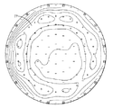
図1は、従来の誘電堆積チャンバ30の横断面図を示す。堆積チャンバ30は、ペデスタル32と、チャンバ壁34と、ガス配給組立体ないしシャワーヘッド40を備えている。シャワーヘッド40は、典型的にはチャンバ内で電極として機能する平坦な下面を示す。しかし、PECVDプロセス及び図1に示したようなハードウェアでは、プロセスによっては、堆積の均一性、再現性や信頼性における問題を示してきた。例えば図2は、図1に示す従来のチャンバを用いて処理される基板上の典型的なプラズマ電荷密度を示す。図示のように、プラズマ電荷密度は、基板の全面について均一でない。さらに、参照番号77で示すように、プラズマ密度は、中心よりも基板の端の方で大きくなっている。典型的には、堆積均一性は、電極の周囲のまわりでプラズマ密度が増大する結果、基板のエッジでは中心と比較してより厚いかより大きい。したがって、堆積プロセスにおけるプラズマエッジ効果を防止して、堆積均一性、再現性及び信頼性を大きく向上させるためのニーズが、コストに有効な解決法のために存在する。
【0007】
【課題を解決するための手段】
本発明は、プラズマガスを基板処理チャンバの処理区域に制限するための装置を提供する。1つの側面では、プラズマを処理チャンバ内に制限するための装置が提供され、これは、環状の電極実装面を有する上側区分と、内側環状制限壁及び外側環状制限壁を有し、上側実装区分と一体的に形成される下側区分とを備えている。内側環状制限壁は、チョークアパーチャを形成するために外側環状の制限壁の方へ、垂直線からある角度で広がっている。別の側面では、環状の電極表面を有する上側区分と、内側制限壁及び外側制限壁を有し上側区分と一体的に形成される下側区分とを備える装置が提供される。さらに別の側面では、プロセスガスを供給するための装置が提供され、この装置は、ガス入口及びガス出口を有するガス配給組立体と、環状の部材とを備え、この環状の部材は、電極実装表面を有する上側区分と、内側環状制限壁及び外側環状制限壁を有し上側区分と一体的に形成される下側区分とを備える。
【0008】
また別の側面では、プラズマを処理チャンバに制限するために処理チャンバはが提供される。処理チャンバは、処理キャビティを画するチャンバ本体と、処理キャビティ内に配置される基板支持部材と、少なくとも1つのガス入口及び少なくとも1つのガス出口を有するガス配給組立体と、環状の部材とを備え、この環状の部材は、電極実装表面を有している上側区分と、内側環状制限壁及び外側環状制限壁を有し上側区分と一体的に形成される下側区分とを備える。
【0009】
上記に挙げた本発明の機能、利点及び目的を達し詳細に理解することができるよう、添付の図面で例示する本発明(簡潔に上に要約した)の特定の説明を、具体例を参照して行う。
【0010】
しかし注意すべきは、添付の図面は本発明の典型的な実施例を例示するだけのものであり、従って範囲を限定するものではなく、本発明の他の等しく有効な具体例も許される。
【0011】
【発明の実施の形態】
本発明は一般に、基板処理チャンバのプラズマ区域内にチョークアパーチャを形成する電極延長部材に関する。チョークアパーチャは、より大きいプラズマ密度が典型的には形成される基板のエッジでプラズマ区域の容量を減らす。延長部材は、少なくともその一部がプラズマ区域の周囲に伸び、基板のエッジのまわりのプラズマの容量を減らす。さらに、電極延長部材は下方へ伸びる部分を提供し、これは、プラズマの横の境界を画する。従って、電極延長部材は処理チャンバの接地された制限壁から離れるようにプラズマを制限し、制限壁への損失を防止する。その結果、より均一な層堆積が基板の全面に対して得られる。
【0012】
多くの基板処理チャンバは、商業的に入手可能である。説明の明瞭さ及び平易のため、以下の説明は主に、米国カリフォルニア州サンタクララのアプライドマテリアルズ社より入手可能でありまた、Zao らの米国特許第5,558,717号に説明されるCVD DXZ チャンバとして知られる処理チャンバを参照する。
【0013】
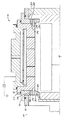
図3は、CVD DXZ チャンバの断面図である。CVD DXZ チャンバ20は、チャンバ本体22を備え、これは典型的にはアルミニウム製であり、プラズマ処理領域24を有する内部の真空チャンバ23を画している。チャンバ20は、支持面34を有するペデスタル32を有し、その上で基板36が所望の材料を化学気相堆積するために支持される。垂直に可動のリフトピン38は、支持面34に対しての基板36の出し入れを容易にする。チャンバ20は更に、チャンバ20にプロセスガス及びパージガスを導入するガス送出組立体40と、基板36の上に堆積させるためのプロセスガスプラズマを生成し維持するためのRF電源50を更に有する。
【0014】
ガス送出組立体40は、チャンバ本体22の上端でベースプレート60の上に配置され、ガス配給フェースプレート42(シャワーヘッドとしてたびたび参照される)と、電極延長部材44と、ブロッカープレート45と、ガス-フィードドラム46とを有している。ガスは、ガス-フィードドラム46に形成される中央ガス入口80によって、ガス送出組立体40に提供される。図示されないが、プロセスガス入口80は、1つ以上の上流側ガスソース及びガスミクサー等他のガス送出部品の一方又は双方に結合される。プロセスガス入口80は、ギャップ261と流体連絡し、このギャップはガスフィードドラム46の下側の面263及びシャワーヘッド42の上面255によって画される。
【0015】
ブロッカープレート45は、ギャップ261内に配置され、ガスフィードカバープレート46に装着される。ブロッカープレート45は好ましくは、アルミニウムアロイ製であり、そこに形成されてガス入口80からシャワーヘッド42までガスを分散させるように構成される通路ないしホール47を有している。
【0016】
シャワーヘッド42は、プロセス領域24に気体流を配給するために構成される複数のホール48と、環状のフランジ49とを有し、このフランジは、ガス送出組立体40を支持するために絶縁リング70の上に配置されるシャワーヘッド40と一体の部品である。シャワーヘッド42は、実質的にディスク形であり、高度に仕上げられた表面を有するアルミニウムアロイ等の熱伝導率が高く熱接触抵抗(Rc)の低い材料から造られる。絶縁リング70と液体に対して緊密な接点を確保するため、シール275が環状の取付けフランジ49に配置されることが好ましい。絶縁リング70は、セラミックのポリマー材料等の非導電性の材料を備えており、接地されたベースプレート60からRF電力を絶縁する。
【0017】
ガスフィードドラム46は、ガスフィードドラム46の周囲に形成される環状の取付けフランジ273を有する。環状の装着フランジ273のサイズは、シャワーヘッド42の周囲の上に配置されるように設定される。シャワーヘッド40と流体に対して緊密な接点を確保するために、環状の装着フランジ273にはシール271が配置されることが好ましい。ガスフィードドラムプレート46は、アルミニウム又はアルミニウムアロイでできていることが好ましい。またガスフィードドラム46は、ガス送出組立体40を所望の温度に維持するための水又は他の流体を有するマルチターンの冷却/加熱チャンネル(図示されず)を有していてもよい。ガスフィードドラム46は、シャワーヘッド42の上に配置され、これに熱的に連絡する。電源50は、プラズマの生成を容易にするため、シャワーヘッド42へ直流(DC)や高周波(RF)等の電力を供給する。
【0018】
電極延長部材44は、環状の部材又はリング形の部材である。一具体例では、電極延長部材44は、図3に示すシャワーヘッド40の周囲に配置される。あるいは下記の図5の説明で述べられるように、電極延長部材44は、基板の表面又はガス送出組立体の下面の一方又は双方に対して共形の形状であってもよい。
【0019】
操作においては、例えばシリコンカーバイド(SiC)膜等の膜が、ロボット(図示されず)とリフトピン38の協働によりペデスタル32上に配置される基板36の上に堆積されてもよい。ペデスタル32は、基板36を上げて、シャワーヘッド42に接近するようにする。例えばトリメチルシラン等を有するプロセスガスと希ガス(ヘリウムやアルゴン等)が、中央ガス入口80を通してチャンバ20内に注入され、そこでは、ガスがブロッカープレート45のホール47を通してシャワーヘッド42の裏面に流入する。矢印で指示するように、プロセスガスは、シャワーヘッド42のホール48を通して処理領域24へ進み、基板36の方へと通過する。基板36に達すれば、プロセスガスはその上面で反応する。その後プロセスガス副生成物は、基板36のエッジを横切って半径方向外向きに流れ、ポンピングチャンネル23に流入し、真空系(図示されず)によってチャンバ20から排気される。SiC膜の堆積中は、チャンバ圧力は3〜10Torrであり、更に好ましくは6〜10Torrである。単一の13.56MHzのRF電源は、約4.3〜10 W/cm2の出力密度で約300-700ワット、また更に好ましくは約5.7〜8.6W/cm2の出力密度で約400〜600ワットでアノード及びカソードに印加し、シリコンベースのガスによりプラズマをチャンバ内に形成する。RF電源は、チャンバに導入される反応性の種の分解を促進するため、典型的には13.56MHzの高RF周波数及び360kHzの低RF周波数で電力を供給する混合周波数RF電源であってもよい。基板表面温度は、約200℃〜400℃、より好ましくは約300℃〜400℃である。
【0020】
ここに説明される堆積ハードウェアは、SiCの堆積に加えて、任意の堆積材料に対して用いられてもよく、例えば他の誘電反射防止コーティング(DARC)材料、酸化物(SiXOY)、炭素ドープ酸化シリコン(SiXOY:C)、炭素ドープ窒化シリコン(SiXNY:C)や低誘電物質等を挙げることができる。
【0021】
図4は、図3に示すガス送出組立体40の破断横断面図である。ガス送出組立体40はシャワーヘッド42を有し、これはその外周に配置される電極延長部材280を有している。電極延長部材280は、下側区分284と一体的に形成される上側区分282を有している。上側区分282は、上側実装表面283と、内側壁288と、外側壁286を有している。下側区分284は、内側制限壁289と、外側制限壁287とを備えている。外側制限壁287の直径は、上側区分282の外側壁286の直径と同じ又は実質的に同じである。内側制限壁289の直径は、上側区分282の内側壁288の直径と同じ又は実質的に同じであり、垂直線より下側区分282の外側制限壁287の寸法に向かって広がっている。内側制限壁289は、約30度〜約70度の角度で広がっている。好ましくは、内側制限壁289は、約45度の角度で広がる。
【0022】
上側区分282の内側制限壁288は、ファスナ298、299(好ましくはボルト)によってシャワーヘッド42の周囲に結合し、良好な電気連絡を確保する。上側区分282は、絶縁リング70の下側面256に適合させるほぼ平坦な上側実装面283を有する。隣接同士をかみ合わせれば、上側実装面283及び下側面256は、ガス送出組立体40の半径方向軸291と平行である境界面を画する。
【0023】
図5は、電極延長部材380の代替具体例を示す破断横断面図である。電極延長部材380は、横方向の拡張が制限される処理チャンバに用いられることが好ましい。電極延長部材380は、上側実装面386と、内側制限壁384と、外側制限壁382を有している。外側制限壁382の直径は、シャワーヘッド42の直径と同じ又は実質的に同じである。内側制限壁384の直径は、基板(図示されず)の直径と同じ又は実質的に同じであり、垂直線から外側制限壁382の方へ広がる。内側制限壁384は、約30度〜約70度の角度で外側制限壁382の方へ広がっている。好ましくは、内側の制限壁384は、外側制限壁382に向かって約45度の角度で広がる。
【0024】
電極延長部材380は、シャワーヘッド42の下側面354上に配置される。電極延長部材380のほぼ平坦な上側実装面386は、良好な電気的連絡を確保するため、ボルトまたは同様のファスナ(図示されず)によってシャワーヘッド42の下側面354に結合する。隣接同士をかみ合わせれば、上側実装表面386と下側面354は、ガス送出組立体349の半径方向の軸391と平行である境界面を画する。
【0025】
電極延長部材280及び380は、高度に仕上げられた表面でアルミニウムアロイ等の高熱伝導率及び低熱接触抵抗(Rc)を有する材料から造られる。電極延長部材280及び380は典型的には、それに配置されるシャワーヘッド42と同じ材料から造られる。あるいは、更なる具体例では、このに説明するように、シャワーヘッド42は、電極延長部材280及び380の下方延長部分を有するよう、アルミニウム又はその他の適切な材料の単一体より削り出して作ってもよい。
【0026】
図3、図4及び図5に示すガス送出組立体40は、環状の部材又はリング形の部材であるように記述されている。しかし、本発明は特定の形状に限定されない。他の幾何学的構成、例えば環状、平行四辺形や他の形状が想定される。
【0027】
本発明は、さらに以下の非限定的な実例で説明される。
【0028】
実施例1
図3に示される処理チャンバを用いて、基板が処理された。923オングストロームの平均厚さを有するシリコンカーバイドの膜が、シリコン基板上に堆積された。堆積均一性は、UV―145SE薄膜測定システムにより測定された。堆積厚さは、基板の表面の端から端までで1.6%の測定標準偏差を有していた。図6から分かるように、基板はドーナツ型の構成を示さず、堆積は基板の表面の端から端まで均一であった。
【0029】
比較例
図1に示す従来のチャンバを用いて、堆積プロセスが実施された。977オングストロームの平均厚さを有するシリコンカーバイドの膜が、シリコン基板上に堆積された。図2に示すように、符号77で示される通り、基板表面の端から端までドーナツ型の構成が存在した。堆積均一性は、同じくUV―145SE薄膜測定システムによって測定された。堆積厚さは、3.8%の測定標準偏差を有していた。
【0030】
ここまで述べたことは、本発明の好ましい具体例に関するが、本発明の他の具体例や更に進んだ具体例を、基本範囲から離れずに工夫されてもよく、そしてその範囲は特許請求の範囲によって決められる。
【図面の簡単な説明】
【図1】図1は、先行技術の従来の誘電堆積チャンバの横断面図である。
【図2】図2は、図1に示す従来の誘電堆積チャンバを用いて処理される基板のプラズマ電荷密度パターンである。
【図3】図3は、米国カリフォルニア州サンタクララのアプライドマテリアルズ社より入手可能な電極延長部材を有するCVD DXZチャンバの横断面図である。
【図4】図4は、図3に示されるガス送出組立体の破断横断面図である。
【図5】図5は、電極延長部材の別の具体例を示すガス送出システムの横断面図である。
【図6】図6は、環状の電極延長装置を用いた場合の基板のプラズマ電荷密度パターンである。
【符号の説明】
20…チャンバ、22…チャンバ本体、23…真空チャンバ、24…プラズマ処理領域、32…ペデスタル、34…支持面、36…基板、38…リフトピン、50…RF電源。[0001]
BACKGROUND OF THE INVENTION
The present invention relates to a semiconductor processing apparatus. In particular, the present invention relates to an apparatus and a processing chamber for confining plasma gas within a processing area of the processing chamber.
[0002]
[Prior art]
In the manufacture of integrated circuits (ICs) and other electronic devices, a number of conductive, semiconductive, and dielectric layers are deposited and removed from the surface of the substrate. Integrated circuit devices have horizontal and vertical conductive paths. Horizontal conductive paths or interconnects are typically referred to as lines, while vertical conductive paths or interconnects are typically referred to as contacts or vias. The contacts extend to the device above the underlying substrate and the vias extend to the underlying metal layer.
[0003]
The formation, deposition, and removal of conductive, semiconducting, and dielectric thin films depend on a variety of techniques. Common deposition techniques in the latest processing methods include physical vapor deposition (PVD), also known as sputtering, chemical vapor deposition (CVD), plasma enhanced chemical vapor deposition (PECVD), electroplating, and the like.
[0004]
In a chemical vapor deposition (CVD) process, a substrate is exposed to a precursor gas, which reacts on the surface of the substrate, deposits reaction products on the substrate, and grows a film thereon. . This surface reaction can be carried out by at least two different methods. In a thermal process, the substrate is heated to a sufficiently high temperature to provide the activation energy necessary for the precursor gas in contact with the substrate to react and deposit a layer on the substrate. In the PECVD process, the precursor gas has an electromagnetic field high enough to excite the precursor gas and obtain energy such as ions and radicals that react on the substrate surface to form the desired material. receive.
[0005]
PECVD is one process used in the manufacture of semiconductor devices to deposit silicon carbide (SiC) on various substrates. Silicon carbide is a useful material for barrier layers and etch stops in IC applications, and as a useful material for multilevel anti-reflective coatings (arcs), including pre-metal dielectric (PMD) levels. . The PECVD process for depositing SiC has an operation of introducing silane gas (SiH 4 ) and methane gas (CH 4 ) into the processing chamber, where the gas reacts and silicon is deposited on the substrate placed in the chamber. A carbide film layer is formed. Gas distribution assemblies are commonly utilized in PECVD chambers to distribute gas evenly over the substrate surface upon introduction of gas into the chamber. Uniform gas delivery is excellent for forming a uniform SiC deposit on the surface of the substrate.
[0006]
[Problems to be solved by the invention]
FIG. 1 shows a cross-sectional view of a conventional
[0007]
[Means for Solving the Problems]
The present invention provides an apparatus for limiting plasma gas to a processing area of a substrate processing chamber. In one aspect, an apparatus is provided for confining a plasma within a processing chamber, which includes an upper section having an annular electrode mounting surface, an inner annular restriction wall, and an outer annular restriction wall, the upper mounting section. And a lower section formed integrally with each other. The inner annular limiting wall extends at an angle from the vertical to the outer annular limiting wall to form a choke aperture. In another aspect, an apparatus is provided comprising an upper section having an annular electrode surface and a lower section having an inner and outer limiting wall and integrally formed with the upper section. In yet another aspect, an apparatus for supplying process gas is provided, the apparatus comprising a gas distribution assembly having a gas inlet and a gas outlet, and an annular member, the annular member comprising an electrode mounting An upper section having a surface and a lower section having an inner annular restriction wall and an outer annular restriction wall and integrally formed with the upper section.
[0008]
In yet another aspect, a processing chamber is provided to limit the plasma to the processing chamber. The processing chamber includes a chamber body defining a processing cavity, a substrate support member disposed within the processing cavity, a gas distribution assembly having at least one gas inlet and at least one gas outlet, and an annular member. The annular member includes an upper section having an electrode mounting surface and a lower section having an inner annular restriction wall and an outer annular restriction wall and formed integrally with the upper section.
[0009]
In order that the above-described functions, advantages and objects of the invention may be attained and understood in detail, the specific description of the invention (simply summarized above) illustrated in the accompanying drawings will be referred to with specific examples. Do it.
[0010]
It should be noted, however, that the accompanying drawings are merely illustrative of exemplary embodiments of the invention and are not intended to limit the scope, and other equally valid embodiments of the invention are allowed.
[0011]
DETAILED DESCRIPTION OF THE INVENTION
The present invention generally relates to an electrode extension member that forms a choke aperture in a plasma zone of a substrate processing chamber. The choke aperture reduces the volume of the plasma zone at the edge of the substrate where a higher plasma density is typically formed. The extension member extends at least in part around the plasma zone and reduces the volume of plasma around the edge of the substrate. In addition, the electrode extension member provides a downwardly extending portion that defines a lateral boundary of the plasma. Thus, the electrode extension member limits the plasma away from the grounded limiting wall of the processing chamber and prevents loss to the limiting wall. As a result, a more uniform layer deposition is obtained over the entire surface of the substrate.
[0012]
Many substrate processing chambers are commercially available. For clarity and simplicity of description, the following description is primarily available from Applied Materials, Inc., Santa Clara, Calif., And is described in US Pat. No. 5,558,717 to Zao et al. Reference is made to the processing chamber known as the DXZ chamber.
[0013]
FIG. 3 is a cross-sectional view of a CVD DXZ chamber. The
[0014]
The
[0015]
The
[0016]
The
[0017]
The
[0018]
The electrode extension member 44 is an annular member or a ring-shaped member. In one specific example, the electrode extending member 44 is disposed around the
[0019]
In operation, a film such as a silicon carbide (SiC) film, for example, may be deposited on the
[0020]
The deposition hardware described herein may be used for any deposition material in addition to SiC deposition, such as other dielectric anti-reflective coating (DARC) materials, oxides (Si x O y ). And carbon-doped silicon oxide (Si x O y : C), carbon-doped silicon nitride (Si x N y : C), and low dielectric materials.
[0021]
4 is a cutaway cross-sectional view of the
[0022]
The inner limiting
[0023]
FIG. 5 is a cutaway cross-sectional view showing an alternative specific example of the
[0024]
The
[0025]
The
[0026]
The
[0027]
The invention is further illustrated by the following non-limiting examples.
[0028]
Example 1
The substrate was processed using the processing chamber shown in FIG. A film of silicon carbide having an average thickness of 923 angstroms was deposited on the silicon substrate. The deposition uniformity was measured with a UV-145SE thin film measurement system. The deposition thickness had a measured standard deviation of 1.6% across the surface of the substrate. As can be seen from FIG. 6, the substrate did not exhibit a donut-shaped configuration and the deposition was uniform across the surface of the substrate.
[0029]
Comparative Example A deposition process was performed using the conventional chamber shown in FIG. A film of silicon carbide having an average thickness of 977 Å was deposited on the silicon substrate. As shown in FIG. 2, as indicated by
[0030]
Although what has been described so far relates to preferred embodiments of the present invention, other embodiments of the present invention and further embodiments may be devised without departing from the basic scope thereof, which scope is claimed. Determined by range.
[Brief description of the drawings]
FIG. 1 is a cross-sectional view of a prior art conventional dielectric deposition chamber.
FIG. 2 is a plasma charge density pattern of a substrate processed using the conventional dielectric deposition chamber shown in FIG.
FIG. 3 is a cross-sectional view of a CVD DXZ chamber with electrode extension members available from Applied Materials, Inc., Santa Clara, California, USA.
FIG. 4 is a cutaway cross-sectional view of the gas delivery assembly shown in FIG.
FIG. 5 is a cross-sectional view of a gas delivery system showing another specific example of an electrode extension member.
FIG. 6 is a plasma charge density pattern of a substrate when an annular electrode extension device is used.
[Explanation of symbols]
DESCRIPTION OF
Claims (13)
上側取付面(256;386)と、内側環状制限壁(289;384)と外側環状制限壁(287;382)とを有し、内側環状制限壁(289;384)が、垂直線からある角度で外側環状制限壁(287;382)に向かって広がっている、環状部材(280;380)と、
前記環状部材(280;380)を装着したガス配給アセンブリ(40)と、
を備え、
前記環状部材(280;380)は、下端の位置が基板の位置に対応する高さになるように、下方に伸びている、
装置。An apparatus for delivering process gas into a substrate processing chamber,
It has an upper mounting surface (256; 386), an inner annular restricting wall (289; 384) and an outer annular restricting wall (287; 382), and the inner annular restricting wall (289; 384) is at an angle from the vertical line. An annular member (280; 380) extending toward the outer annular restriction wall (287; 382) at
A gas delivery assembly (40) fitted with the annular member (280; 380);
With
The annular member (280; 380) extends downward so that the position of the lower end is a height corresponding to the position of the substrate.
apparatus.
処理キャビティを画すチャンバ本体と、
処理キャビティ内に配置される基板支持部材と、
上側取付面(386)と、内側環状制限壁(384)と外側環状制限壁(382)とを有し、内側環状制限壁(384)が、垂直線からある角度で外側環状制限壁(382)に向かって広がっている、環状部材(380)と、
複数の通気孔が形成されたガス配給アセンブリ(40)であって、縁部に前記環状部材(380)の上側取付面(386)が実装され、外径が前記外側環状制限壁(382)の外径に略等しい、ガス配給アセンブリ(40)と、
前記ガス供給アセンブリ(40)を支持する絶縁リング(70)であって、絶縁リング(70)の上部は、チャンバ本体とガス配給アセンブリ(40)の外縁部との間に介挿され、絶縁リング(70)の下部は前記外側環状制限壁(382)に連結される、絶縁リング(70)と、
を備え、
前記環状部材(380)は、下端の位置が基板の位置に対応する高さになるように、下方に伸びている、
処理チャンバ。A processing chamber,
A chamber body defining a processing cavity;
A substrate support member disposed within the processing cavity;
It has an upper mounting surface (386), an inner annular restricting wall (384) and an outer annular restricting wall (382), the inner annular restricting wall (384) being an outer annular restricting wall (382) at an angle from the vertical line. An annular member (380) extending toward
A gas distribution assembly (40) having a plurality of vent holes, wherein an upper mounting surface (386) of the annular member (380) is mounted on an edge and an outer diameter of the outer annular restriction wall (382). A gas distribution assembly (40) substantially equal to the outer diameter;
An insulating ring (70) for supporting the gas supply assembly (40), wherein an upper portion of the insulating ring (70) is interposed between the chamber body and the outer edge of the gas distribution assembly (40), An insulating ring (70) connected to the outer annular restriction wall (382) at a lower portion of (70);
With
The annular member (380) extends downward so that the position of the lower end is a height corresponding to the position of the substrate.
Processing chamber.
処理キャビティを画するチャンバ本体と、
処理キャビティ内に配置される基板支持部材と、
複数の通気孔が形成されたガス配給アセンブリ(40)と、
前記ガス供給アセンブリ(40)を支持する絶縁リング(70)であって、絶縁リング(70)の一部は、チャンバ本体とガス配給アセンブリ(40)の外縁部との間に介挿される、絶縁リング(70)と、
前記絶縁リング(70)の下面に連結する上側取付面(256)を有する環状部材(280)であって、前記ガス配給アセンブリ(40)の底面の下方へ延長している、環状部材(280)と、
を備え、
前記環状部材(280)は、下端の位置が基板の位置に対応する高さになるように、下方に伸びている、
処理チャンバ。A processing chamber,
A chamber body defining a processing cavity;
A substrate support member disposed within the processing cavity;
A gas distribution assembly (40) formed with a plurality of vents;
An insulating ring (70) supporting the gas supply assembly (40), wherein a portion of the insulating ring (70) is interposed between the chamber body and the outer edge of the gas distribution assembly (40). A ring (70);
An annular member (280) having an upper mounting surface ( 256 ) coupled to the lower surface of the insulating ring (70), the annular member (280) extending below the bottom surface of the gas distribution assembly (40). When,
With
The annular member (280) extends downward so that the position of the lower end is a height corresponding to the position of the substrate.
Processing chamber.
ガス配給アセンブリ(40)と、
前記ガス配給アセンブリ(40)の底面の一部に連結された環状部材(380)であって、内側環状制限壁(384)と外側環状制限壁(382)とを有し、前記ガス配給アセンブリ(40)の外径が前記外側環状制限壁(382)の外径に略等しい、環状部材(380)と、
前記ガス供給アセンブリ(40)を支持する絶縁リング(70)であって、絶縁リング(70)の上部は、前記ガス配給アセンブリ(40)の外縁部と前記基板処理チャンバの側壁部との間に介挿され、絶縁リング(70)の下部は前記環状部材(380)の外側環状制限壁(382)に連結される、絶縁リング(70)と、
を備え、
前記環状部材(380)は、下端の位置が基板の位置に対応する高さになるように、下方に伸びている、
装置。 An apparatus for delivering process gas into a substrate processing chamber,
A gas distribution assembly (40);
An annular member (380) coupled to a portion of the bottom surface of the gas distribution assembly (40), comprising an inner annular restriction wall (384) and an outer annular restriction wall (382), wherein the gas distribution assembly ( An annular member (380), the outer diameter of 40) being substantially equal to the outer diameter of the outer annular restricting wall (382);
An insulating ring (70) supporting the gas supply assembly (40), wherein an upper portion of the insulating ring (70) is between an outer edge of the gas distribution assembly (40) and a side wall of the substrate processing chamber. An insulating ring (70) interposed and connected to an outer annular restriction wall (382) of the annular member (380) at a lower portion of the insulating ring (70);
With
The annular member (380) extends downward so that the position of the lower end is a height corresponding to the position of the substrate.
apparatus.
Applications Claiming Priority (2)
| Application Number | Priority Date | Filing Date | Title |
|---|---|---|---|
| US20373200P | 2000-05-12 | 2000-05-12 | |
| US60/203732 | 2000-05-12 |
Publications (3)
| Publication Number | Publication Date |
|---|---|
| JP2002158179A JP2002158179A (en) | 2002-05-31 |
| JP2002158179A5 JP2002158179A5 (en) | 2006-06-29 |
| JP4808330B2 true JP4808330B2 (en) | 2011-11-02 |
Family
ID=22755097
Family Applications (1)
| Application Number | Title | Priority Date | Filing Date |
|---|---|---|---|
| JP2001143503A Expired - Fee Related JP4808330B2 (en) | 2000-05-12 | 2001-05-14 | Process gas distribution apparatus and processing chamber |
Country Status (6)
| Country | Link |
|---|---|
| US (1) | US6553932B2 (en) |
| EP (1) | EP1154040B1 (en) |
| JP (1) | JP4808330B2 (en) |
| KR (1) | KR100728651B1 (en) |
| DE (1) | DE60136031D1 (en) |
| TW (1) | TW495816B (en) |
Families Citing this family (319)
| Publication number | Priority date | Publication date | Assignee | Title |
|---|---|---|---|---|
| US6905079B2 (en) * | 2000-09-08 | 2005-06-14 | Tokyo Electron Limited | Shower head structure and cleaning method thereof |
| US6660662B2 (en) * | 2001-01-26 | 2003-12-09 | Applied Materials, Inc. | Method of reducing plasma charge damage for plasma processes |
| JP2005536042A (en) * | 2002-08-08 | 2005-11-24 | トリコン テクノロジーズ リミティド | Improved shower head |
| KR100540992B1 (en) * | 2002-11-18 | 2006-01-11 | 코리아세미텍 주식회사 | Cathode for wafer etching the manufacturing method thereof |
| KR100585089B1 (en) * | 2003-05-27 | 2006-05-30 | 삼성전자주식회사 | Plasma processing apparatus for processing the edge of wafer, insulating plate for plasma processing, bottom electrode for plasma processing, method of plasma processing the edge of wafer and method of fabricating semiconductor device using the same |
| US20050100682A1 (en) * | 2003-11-06 | 2005-05-12 | Tokyo Electron Limited | Method for depositing materials on a substrate |
| US20050230350A1 (en) * | 2004-02-26 | 2005-10-20 | Applied Materials, Inc. | In-situ dry clean chamber for front end of line fabrication |
| US20050223983A1 (en) * | 2004-04-08 | 2005-10-13 | Venkat Selvamanickam | Chemical vapor deposition (CVD) apparatus usable in the manufacture of superconducting conductors |
| US20050223984A1 (en) * | 2004-04-08 | 2005-10-13 | Hee-Gyoun Lee | Chemical vapor deposition (CVD) apparatus usable in the manufacture of superconducting conductors |
| KR20060014495A (en) * | 2004-08-11 | 2006-02-16 | 주식회사 유진테크 | Shower head of chemical vapor deposition apparatus |
| US7452660B1 (en) * | 2004-08-11 | 2008-11-18 | Lam Research Corporation | Method for resist strip in presence of low K dielectric material and apparatus for performing the same |
| US7387811B2 (en) * | 2004-09-21 | 2008-06-17 | Superpower, Inc. | Method for manufacturing high temperature superconducting conductors using chemical vapor deposition (CVD) |
| US8535443B2 (en) * | 2005-07-27 | 2013-09-17 | Applied Materials, Inc. | Gas line weldment design and process for CVD aluminum |
| KR100734775B1 (en) * | 2005-09-15 | 2007-07-04 | 주식회사 아이피에스 | Showerhead |
| US8232176B2 (en) | 2006-06-22 | 2012-07-31 | Applied Materials, Inc. | Dielectric deposition and etch back processes for bottom up gapfill |
| KR100829922B1 (en) * | 2006-08-24 | 2008-05-16 | 세메스 주식회사 | Apparatus and method for treating substrates using plasma |
| KR100769522B1 (en) | 2006-10-25 | 2007-11-06 | 주식회사 유진테크 | Shower head of chemical vapor deposition apparatus |
| ES2331489T3 (en) * | 2007-03-05 | 2010-01-05 | Applied Materials, Inc. | COATING SYSTEM AND GAS DRIVING SYSTEM. |
| US7867923B2 (en) * | 2007-10-22 | 2011-01-11 | Applied Materials, Inc. | High quality silicon oxide films by remote plasma CVD from disilane precursors |
| JP5218942B2 (en) * | 2008-02-06 | 2013-06-26 | 株式会社ユーテック | Plasma CVD apparatus, plasma CVD method and stirring apparatus |
| US8357435B2 (en) | 2008-05-09 | 2013-01-22 | Applied Materials, Inc. | Flowable dielectric equipment and processes |
| US8221582B2 (en) | 2008-07-07 | 2012-07-17 | Lam Research Corporation | Clamped monolithic showerhead electrode |
| US8161906B2 (en) * | 2008-07-07 | 2012-04-24 | Lam Research Corporation | Clamped showerhead electrode assembly |
| US8206506B2 (en) * | 2008-07-07 | 2012-06-26 | Lam Research Corporation | Showerhead electrode |
| US9493875B2 (en) | 2008-09-30 | 2016-11-15 | Eugene Technology Co., Ltd. | Shower head unit and chemical vapor deposition apparatus |
| KR200452532Y1 (en) * | 2008-11-06 | 2011-03-07 | 주식회사 테스 | Gas injection unit |
| US8540844B2 (en) * | 2008-12-19 | 2013-09-24 | Lam Research Corporation | Plasma confinement structures in plasma processing systems |
| US8627783B2 (en) * | 2008-12-19 | 2014-01-14 | Lam Research Corporation | Combined wafer area pressure control and plasma confinement assembly |
| US8869741B2 (en) * | 2008-12-19 | 2014-10-28 | Lam Research Corporation | Methods and apparatus for dual confinement and ultra-high pressure in an adjustable gap plasma chamber |
| US9394608B2 (en) | 2009-04-06 | 2016-07-19 | Asm America, Inc. | Semiconductor processing reactor and components thereof |
| US8402918B2 (en) * | 2009-04-07 | 2013-03-26 | Lam Research Corporation | Showerhead electrode with centering feature |
| US8272346B2 (en) | 2009-04-10 | 2012-09-25 | Lam Research Corporation | Gasket with positioning feature for clamped monolithic showerhead electrode |
| US8980382B2 (en) | 2009-12-02 | 2015-03-17 | Applied Materials, Inc. | Oxygen-doping for non-carbon radical-component CVD films |
| US8741788B2 (en) | 2009-08-06 | 2014-06-03 | Applied Materials, Inc. | Formation of silicon oxide using non-carbon flowable CVD processes |
| US8802201B2 (en) | 2009-08-14 | 2014-08-12 | Asm America, Inc. | Systems and methods for thin-film deposition of metal oxides using excited nitrogen-oxygen species |
| TWM412457U (en) * | 2009-09-18 | 2011-09-21 | Lam Res Corp | Showerhead electrode for use in a plasma reaction chamber and showerhead electrode assembly |
| KR200464037Y1 (en) * | 2009-10-13 | 2012-12-07 | 램 리써치 코포레이션 | - edge-clamped and mechanically fastened inner electrode of showerhead electrode assembly |
| US8449942B2 (en) | 2009-11-12 | 2013-05-28 | Applied Materials, Inc. | Methods of curing non-carbon flowable CVD films |
| US8629067B2 (en) | 2009-12-30 | 2014-01-14 | Applied Materials, Inc. | Dielectric film growth with radicals produced using flexible nitrogen/hydrogen ratio |
| US8329262B2 (en) | 2010-01-05 | 2012-12-11 | Applied Materials, Inc. | Dielectric film formation using inert gas excitation |
| CN102754193A (en) | 2010-01-06 | 2012-10-24 | 应用材料公司 | Flowable dielectric using oxide liner |
| SG182333A1 (en) * | 2010-01-07 | 2012-08-30 | Applied Materials Inc | In-situ ozone cure for radical-component cvd |
| US20110206833A1 (en) * | 2010-02-22 | 2011-08-25 | Lam Research Corporation | Extension electrode of plasma bevel etching apparatus and method of manufacture thereof |
| JP2013521650A (en) | 2010-03-05 | 2013-06-10 | アプライド マテリアルズ インコーポレイテッド | Conformal layer by radical component CVD |
| CN102934203B (en) * | 2010-04-28 | 2015-09-23 | 应用材料公司 | For the process chamber chamber cap design with built-in plasma source of short-life-cycle species |
| US8573152B2 (en) | 2010-09-03 | 2013-11-05 | Lam Research Corporation | Showerhead electrode |
| US9285168B2 (en) | 2010-10-05 | 2016-03-15 | Applied Materials, Inc. | Module for ozone cure and post-cure moisture treatment |
| US8664127B2 (en) | 2010-10-15 | 2014-03-04 | Applied Materials, Inc. | Two silicon-containing precursors for gapfill enhancing dielectric liner |
| KR20120043636A (en) * | 2010-10-26 | 2012-05-04 | 가부시키가이샤 한도오따이 에네루기 켄큐쇼 | Plasma treatment apparatus and plasma cvd apparatus |
| US10283321B2 (en) | 2011-01-18 | 2019-05-07 | Applied Materials, Inc. | Semiconductor processing system and methods using capacitively coupled plasma |
| US8450191B2 (en) | 2011-01-24 | 2013-05-28 | Applied Materials, Inc. | Polysilicon films by HDP-CVD |
| US8716154B2 (en) | 2011-03-04 | 2014-05-06 | Applied Materials, Inc. | Reduced pattern loading using silicon oxide multi-layers |
| US8445078B2 (en) | 2011-04-20 | 2013-05-21 | Applied Materials, Inc. | Low temperature silicon oxide conversion |
| US8466073B2 (en) | 2011-06-03 | 2013-06-18 | Applied Materials, Inc. | Capping layer for reduced outgassing |
| US9312155B2 (en) | 2011-06-06 | 2016-04-12 | Asm Japan K.K. | High-throughput semiconductor-processing apparatus equipped with multiple dual-chamber modules |
| US9404178B2 (en) | 2011-07-15 | 2016-08-02 | Applied Materials, Inc. | Surface treatment and deposition for reduced outgassing |
| US20130023129A1 (en) | 2011-07-20 | 2013-01-24 | Asm America, Inc. | Pressure transmitter for a semiconductor processing environment |
| HUP1100436A2 (en) * | 2011-08-15 | 2013-02-28 | Ecosolifer Ag | Gas flow system for using in reaction chamber |
| US8617989B2 (en) | 2011-09-26 | 2013-12-31 | Applied Materials, Inc. | Liner property improvement |
| US8551891B2 (en) | 2011-10-04 | 2013-10-08 | Applied Materials, Inc. | Remote plasma burn-in |
| US9017481B1 (en) | 2011-10-28 | 2015-04-28 | Asm America, Inc. | Process feed management for semiconductor substrate processing |
| KR101327458B1 (en) * | 2012-01-10 | 2013-11-08 | 주식회사 유진테크 | Showerhead having cooling system and substrate processing apparatus including the showerhead |
| KR102086795B1 (en) * | 2012-06-11 | 2020-04-14 | 세메스 주식회사 | Apparatus and method for treating a substrate |
| US8889566B2 (en) | 2012-09-11 | 2014-11-18 | Applied Materials, Inc. | Low cost flowable dielectric films |
| US10714315B2 (en) | 2012-10-12 | 2020-07-14 | Asm Ip Holdings B.V. | Semiconductor reaction chamber showerhead |
| KR101477602B1 (en) * | 2012-10-30 | 2014-12-30 | 피에스케이 주식회사 | Apparatus for treatimg substrate |
| KR102017744B1 (en) | 2012-12-12 | 2019-10-15 | 삼성디스플레이 주식회사 | Deposition apparatus, method for forming thin film using the same and method for manufacturing organic light emitting display apparatus |
| US9018108B2 (en) | 2013-01-25 | 2015-04-28 | Applied Materials, Inc. | Low shrinkage dielectric films |
| US20160376700A1 (en) | 2013-02-01 | 2016-12-29 | Asm Ip Holding B.V. | System for treatment of deposition reactor |
| US10808317B2 (en) | 2013-07-03 | 2020-10-20 | Lam Research Corporation | Deposition apparatus including an isothermal processing zone |
| US10683571B2 (en) | 2014-02-25 | 2020-06-16 | Asm Ip Holding B.V. | Gas supply manifold and method of supplying gases to chamber using same |
| US9741575B2 (en) | 2014-03-10 | 2017-08-22 | Taiwan Semiconductor Manufacturing Co., Ltd. | CVD apparatus with gas delivery ring |
| US11015245B2 (en) | 2014-03-19 | 2021-05-25 | Asm Ip Holding B.V. | Gas-phase reactor and system having exhaust plenum and components thereof |
| US9412581B2 (en) | 2014-07-16 | 2016-08-09 | Applied Materials, Inc. | Low-K dielectric gapfill by flowable deposition |
| US10858737B2 (en) | 2014-07-28 | 2020-12-08 | Asm Ip Holding B.V. | Showerhead assembly and components thereof |
| US9890456B2 (en) | 2014-08-21 | 2018-02-13 | Asm Ip Holding B.V. | Method and system for in situ formation of gas-phase compounds |
| US10941490B2 (en) | 2014-10-07 | 2021-03-09 | Asm Ip Holding B.V. | Multiple temperature range susceptor, assembly, reactor and system including the susceptor, and methods of using the same |
| US10276355B2 (en) | 2015-03-12 | 2019-04-30 | Asm Ip Holding B.V. | Multi-zone reactor, system including the reactor, and method of using the same |
| US10458018B2 (en) | 2015-06-26 | 2019-10-29 | Asm Ip Holding B.V. | Structures including metal carbide material, devices including the structures, and methods of forming same |
| US10211308B2 (en) | 2015-10-21 | 2019-02-19 | Asm Ip Holding B.V. | NbMC layers |
| US11139308B2 (en) | 2015-12-29 | 2021-10-05 | Asm Ip Holding B.V. | Atomic layer deposition of III-V compounds to form V-NAND devices |
| US10529554B2 (en) | 2016-02-19 | 2020-01-07 | Asm Ip Holding B.V. | Method for forming silicon nitride film selectively on sidewalls or flat surfaces of trenches |
| US10865475B2 (en) | 2016-04-21 | 2020-12-15 | Asm Ip Holding B.V. | Deposition of metal borides and silicides |
| US10190213B2 (en) | 2016-04-21 | 2019-01-29 | Asm Ip Holding B.V. | Deposition of metal borides |
| US10367080B2 (en) | 2016-05-02 | 2019-07-30 | Asm Ip Holding B.V. | Method of forming a germanium oxynitride film |
| US10032628B2 (en) | 2016-05-02 | 2018-07-24 | Asm Ip Holding B.V. | Source/drain performance through conformal solid state doping |
| US11453943B2 (en) | 2016-05-25 | 2022-09-27 | Asm Ip Holding B.V. | Method for forming carbon-containing silicon/metal oxide or nitride film by ALD using silicon precursor and hydrocarbon precursor |
| US9859151B1 (en) | 2016-07-08 | 2018-01-02 | Asm Ip Holding B.V. | Selective film deposition method to form air gaps |
| US10612137B2 (en) | 2016-07-08 | 2020-04-07 | Asm Ip Holdings B.V. | Organic reactants for atomic layer deposition |
| US10714385B2 (en) | 2016-07-19 | 2020-07-14 | Asm Ip Holding B.V. | Selective deposition of tungsten |
| US9887082B1 (en) | 2016-07-28 | 2018-02-06 | Asm Ip Holding B.V. | Method and apparatus for filling a gap |
| US9812320B1 (en) | 2016-07-28 | 2017-11-07 | Asm Ip Holding B.V. | Method and apparatus for filling a gap |
| KR102532607B1 (en) | 2016-07-28 | 2023-05-15 | 에이에스엠 아이피 홀딩 비.브이. | Substrate processing apparatus and method of operating the same |
| KR102625574B1 (en) * | 2016-10-06 | 2024-01-16 | 주성엔지니어링(주) | Showerhead of substrate processing apparatus |
| US10643826B2 (en) | 2016-10-26 | 2020-05-05 | Asm Ip Holdings B.V. | Methods for thermally calibrating reaction chambers |
| US11532757B2 (en) | 2016-10-27 | 2022-12-20 | Asm Ip Holding B.V. | Deposition of charge trapping layers |
| US10229833B2 (en) | 2016-11-01 | 2019-03-12 | Asm Ip Holding B.V. | Methods for forming a transition metal nitride film on a substrate by atomic layer deposition and related semiconductor device structures |
| US10714350B2 (en) | 2016-11-01 | 2020-07-14 | ASM IP Holdings, B.V. | Methods for forming a transition metal niobium nitride film on a substrate by atomic layer deposition and related semiconductor device structures |
| KR102546317B1 (en) | 2016-11-15 | 2023-06-21 | 에이에스엠 아이피 홀딩 비.브이. | Gas supply unit and substrate processing apparatus including the same |
| KR20180068582A (en) | 2016-12-14 | 2018-06-22 | 에이에스엠 아이피 홀딩 비.브이. | Substrate processing apparatus |
| US11447861B2 (en) | 2016-12-15 | 2022-09-20 | Asm Ip Holding B.V. | Sequential infiltration synthesis apparatus and a method of forming a patterned structure |
| US11581186B2 (en) | 2016-12-15 | 2023-02-14 | Asm Ip Holding B.V. | Sequential infiltration synthesis apparatus |
| KR20180070971A (en) | 2016-12-19 | 2018-06-27 | 에이에스엠 아이피 홀딩 비.브이. | Substrate processing apparatus |
| US10269558B2 (en) | 2016-12-22 | 2019-04-23 | Asm Ip Holding B.V. | Method of forming a structure on a substrate |
| US10867788B2 (en) | 2016-12-28 | 2020-12-15 | Asm Ip Holding B.V. | Method of forming a structure on a substrate |
| US11390950B2 (en) | 2017-01-10 | 2022-07-19 | Asm Ip Holding B.V. | Reactor system and method to reduce residue buildup during a film deposition process |
| US10655221B2 (en) | 2017-02-09 | 2020-05-19 | Asm Ip Holding B.V. | Method for depositing oxide film by thermal ALD and PEALD |
| US10468261B2 (en) | 2017-02-15 | 2019-11-05 | Asm Ip Holding B.V. | Methods for forming a metallic film on a substrate by cyclical deposition and related semiconductor device structures |
| US10529563B2 (en) | 2017-03-29 | 2020-01-07 | Asm Ip Holdings B.V. | Method for forming doped metal oxide films on a substrate by cyclical deposition and related semiconductor device structures |
| WO2018187494A1 (en) * | 2017-04-07 | 2018-10-11 | Applied Materials, Inc. | Gas phase particle reduction in pecvd chamber |
| KR102457289B1 (en) | 2017-04-25 | 2022-10-21 | 에이에스엠 아이피 홀딩 비.브이. | Method for depositing a thin film and manufacturing a semiconductor device |
| US10892156B2 (en) | 2017-05-08 | 2021-01-12 | Asm Ip Holding B.V. | Methods for forming a silicon nitride film on a substrate and related semiconductor device structures |
| US10770286B2 (en) | 2017-05-08 | 2020-09-08 | Asm Ip Holdings B.V. | Methods for selectively forming a silicon nitride film on a substrate and related semiconductor device structures |
| US11306395B2 (en) * | 2017-06-28 | 2022-04-19 | Asm Ip Holding B.V. | Methods for depositing a transition metal nitride film on a substrate by atomic layer deposition and related deposition apparatus |
| US10685834B2 (en) | 2017-07-05 | 2020-06-16 | Asm Ip Holdings B.V. | Methods for forming a silicon germanium tin layer and related semiconductor device structures |
| KR20190009245A (en) | 2017-07-18 | 2019-01-28 | 에이에스엠 아이피 홀딩 비.브이. | Methods for forming a semiconductor device structure and related semiconductor device structures |
| US11374112B2 (en) | 2017-07-19 | 2022-06-28 | Asm Ip Holding B.V. | Method for depositing a group IV semiconductor and related semiconductor device structures |
| US11018002B2 (en) | 2017-07-19 | 2021-05-25 | Asm Ip Holding B.V. | Method for selectively depositing a Group IV semiconductor and related semiconductor device structures |
| US10541333B2 (en) | 2017-07-19 | 2020-01-21 | Asm Ip Holding B.V. | Method for depositing a group IV semiconductor and related semiconductor device structures |
| US10590535B2 (en) | 2017-07-26 | 2020-03-17 | Asm Ip Holdings B.V. | Chemical treatment, deposition and/or infiltration apparatus and method for using the same |
| US10770336B2 (en) | 2017-08-08 | 2020-09-08 | Asm Ip Holding B.V. | Substrate lift mechanism and reactor including same |
| US10692741B2 (en) | 2017-08-08 | 2020-06-23 | Asm Ip Holdings B.V. | Radiation shield |
| US10249524B2 (en) | 2017-08-09 | 2019-04-02 | Asm Ip Holding B.V. | Cassette holder assembly for a substrate cassette and holding member for use in such assembly |
| US11769682B2 (en) | 2017-08-09 | 2023-09-26 | Asm Ip Holding B.V. | Storage apparatus for storing cassettes for substrates and processing apparatus equipped therewith |
| US11139191B2 (en) | 2017-08-09 | 2021-10-05 | Asm Ip Holding B.V. | Storage apparatus for storing cassettes for substrates and processing apparatus equipped therewith |
| US11830730B2 (en) | 2017-08-29 | 2023-11-28 | Asm Ip Holding B.V. | Layer forming method and apparatus |
| US11056344B2 (en) | 2017-08-30 | 2021-07-06 | Asm Ip Holding B.V. | Layer forming method |
| US11295980B2 (en) | 2017-08-30 | 2022-04-05 | Asm Ip Holding B.V. | Methods for depositing a molybdenum metal film over a dielectric surface of a substrate by a cyclical deposition process and related semiconductor device structures |
| KR102491945B1 (en) | 2017-08-30 | 2023-01-26 | 에이에스엠 아이피 홀딩 비.브이. | Substrate processing apparatus |
| KR102630301B1 (en) | 2017-09-21 | 2024-01-29 | 에이에스엠 아이피 홀딩 비.브이. | Method of sequential infiltration synthesis treatment of infiltrateable material and structures and devices formed using same |
| US10844484B2 (en) | 2017-09-22 | 2020-11-24 | Asm Ip Holding B.V. | Apparatus for dispensing a vapor phase reactant to a reaction chamber and related methods |
| US10658205B2 (en) | 2017-09-28 | 2020-05-19 | Asm Ip Holdings B.V. | Chemical dispensing apparatus and methods for dispensing a chemical to a reaction chamber |
| US10403504B2 (en) | 2017-10-05 | 2019-09-03 | Asm Ip Holding B.V. | Method for selectively depositing a metallic film on a substrate |
| US10319588B2 (en) | 2017-10-10 | 2019-06-11 | Asm Ip Holding B.V. | Method for depositing a metal chalcogenide on a substrate by cyclical deposition |
| US10923344B2 (en) | 2017-10-30 | 2021-02-16 | Asm Ip Holding B.V. | Methods for forming a semiconductor structure and related semiconductor structures |
| US10910262B2 (en) | 2017-11-16 | 2021-02-02 | Asm Ip Holding B.V. | Method of selectively depositing a capping layer structure on a semiconductor device structure |
| KR102443047B1 (en) | 2017-11-16 | 2022-09-14 | 에이에스엠 아이피 홀딩 비.브이. | Method of processing a substrate and a device manufactured by the same |
| US11022879B2 (en) | 2017-11-24 | 2021-06-01 | Asm Ip Holding B.V. | Method of forming an enhanced unexposed photoresist layer |
| US11127617B2 (en) | 2017-11-27 | 2021-09-21 | Asm Ip Holding B.V. | Storage device for storing wafer cassettes for use with a batch furnace |
| WO2019103610A1 (en) | 2017-11-27 | 2019-05-31 | Asm Ip Holding B.V. | Apparatus including a clean mini environment |
| US10872771B2 (en) | 2018-01-16 | 2020-12-22 | Asm Ip Holding B. V. | Method for depositing a material film on a substrate within a reaction chamber by a cyclical deposition process and related device structures |
| TWI799494B (en) | 2018-01-19 | 2023-04-21 | 荷蘭商Asm 智慧財產控股公司 | Deposition method |
| US11482412B2 (en) | 2018-01-19 | 2022-10-25 | Asm Ip Holding B.V. | Method for depositing a gap-fill layer by plasma-assisted deposition |
| USD903477S1 (en) | 2018-01-24 | 2020-12-01 | Asm Ip Holdings B.V. | Metal clamp |
| US11018047B2 (en) | 2018-01-25 | 2021-05-25 | Asm Ip Holding B.V. | Hybrid lift pin |
| USD880437S1 (en) | 2018-02-01 | 2020-04-07 | Asm Ip Holding B.V. | Gas supply plate for semiconductor manufacturing apparatus |
| US11081345B2 (en) | 2018-02-06 | 2021-08-03 | Asm Ip Holding B.V. | Method of post-deposition treatment for silicon oxide film |
| US10896820B2 (en) | 2018-02-14 | 2021-01-19 | Asm Ip Holding B.V. | Method for depositing a ruthenium-containing film on a substrate by a cyclical deposition process |
| KR102657269B1 (en) | 2018-02-14 | 2024-04-16 | 에이에스엠 아이피 홀딩 비.브이. | Method for depositing a ruthenium-containing film on a substrate by a cyclic deposition process |
| US10731249B2 (en) | 2018-02-15 | 2020-08-04 | Asm Ip Holding B.V. | Method of forming a transition metal containing film on a substrate by a cyclical deposition process, a method for supplying a transition metal halide compound to a reaction chamber, and related vapor deposition apparatus |
| KR102636427B1 (en) | 2018-02-20 | 2024-02-13 | 에이에스엠 아이피 홀딩 비.브이. | Substrate processing method and apparatus |
| US10975470B2 (en) | 2018-02-23 | 2021-04-13 | Asm Ip Holding B.V. | Apparatus for detecting or monitoring for a chemical precursor in a high temperature environment |
| US11473195B2 (en) | 2018-03-01 | 2022-10-18 | Asm Ip Holding B.V. | Semiconductor processing apparatus and a method for processing a substrate |
| US11629406B2 (en) | 2018-03-09 | 2023-04-18 | Asm Ip Holding B.V. | Semiconductor processing apparatus comprising one or more pyrometers for measuring a temperature of a substrate during transfer of the substrate |
| US11114283B2 (en) | 2018-03-16 | 2021-09-07 | Asm Ip Holding B.V. | Reactor, system including the reactor, and methods of manufacturing and using same |
| KR102646467B1 (en) | 2018-03-27 | 2024-03-11 | 에이에스엠 아이피 홀딩 비.브이. | Method of forming an electrode on a substrate and a semiconductor device structure including an electrode |
| US11088002B2 (en) | 2018-03-29 | 2021-08-10 | Asm Ip Holding B.V. | Substrate rack and a substrate processing system and method |
| US11230766B2 (en) | 2018-03-29 | 2022-01-25 | Asm Ip Holding B.V. | Substrate processing apparatus and method |
| KR102501472B1 (en) | 2018-03-30 | 2023-02-20 | 에이에스엠 아이피 홀딩 비.브이. | Substrate processing method |
| TWI811348B (en) | 2018-05-08 | 2023-08-11 | 荷蘭商Asm 智慧財產控股公司 | Methods for depositing an oxide film on a substrate by a cyclical deposition process and related device structures |
| KR20190129718A (en) | 2018-05-11 | 2019-11-20 | 에이에스엠 아이피 홀딩 비.브이. | Methods for forming a doped metal carbide film on a substrate and related semiconductor device structures |
| KR102596988B1 (en) | 2018-05-28 | 2023-10-31 | 에이에스엠 아이피 홀딩 비.브이. | Method of processing a substrate and a device manufactured by the same |
| US11718913B2 (en) | 2018-06-04 | 2023-08-08 | Asm Ip Holding B.V. | Gas distribution system and reactor system including same |
| US11270899B2 (en) | 2018-06-04 | 2022-03-08 | Asm Ip Holding B.V. | Wafer handling chamber with moisture reduction |
| US11286562B2 (en) | 2018-06-08 | 2022-03-29 | Asm Ip Holding B.V. | Gas-phase chemical reactor and method of using same |
| US10797133B2 (en) | 2018-06-21 | 2020-10-06 | Asm Ip Holding B.V. | Method for depositing a phosphorus doped silicon arsenide film and related semiconductor device structures |
| KR102568797B1 (en) | 2018-06-21 | 2023-08-21 | 에이에스엠 아이피 홀딩 비.브이. | Substrate processing system |
| KR20210024462A (en) | 2018-06-27 | 2021-03-05 | 에이에스엠 아이피 홀딩 비.브이. | Periodic deposition method for forming metal-containing material and films and structures comprising metal-containing material |
| CN112292477A (en) | 2018-06-27 | 2021-01-29 | Asm Ip私人控股有限公司 | Cyclic deposition methods for forming metal-containing materials and films and structures containing metal-containing materials |
| KR20200002519A (en) | 2018-06-29 | 2020-01-08 | 에이에스엠 아이피 홀딩 비.브이. | Method for depositing a thin film and manufacturing a semiconductor device |
| US10612136B2 (en) | 2018-06-29 | 2020-04-07 | ASM IP Holding, B.V. | Temperature-controlled flange and reactor system including same |
| US10755922B2 (en) | 2018-07-03 | 2020-08-25 | Asm Ip Holding B.V. | Method for depositing silicon-free carbon-containing film as gap-fill layer by pulse plasma-assisted deposition |
| US10388513B1 (en) | 2018-07-03 | 2019-08-20 | Asm Ip Holding B.V. | Method for depositing silicon-free carbon-containing film as gap-fill layer by pulse plasma-assisted deposition |
| US10767789B2 (en) | 2018-07-16 | 2020-09-08 | Asm Ip Holding B.V. | Diaphragm valves, valve components, and methods for forming valve components |
| US11053591B2 (en) | 2018-08-06 | 2021-07-06 | Asm Ip Holding B.V. | Multi-port gas injection system and reactor system including same |
| US10883175B2 (en) | 2018-08-09 | 2021-01-05 | Asm Ip Holding B.V. | Vertical furnace for processing substrates and a liner for use therein |
| US10829852B2 (en) | 2018-08-16 | 2020-11-10 | Asm Ip Holding B.V. | Gas distribution device for a wafer processing apparatus |
| US11430674B2 (en) | 2018-08-22 | 2022-08-30 | Asm Ip Holding B.V. | Sensor array, apparatus for dispensing a vapor phase reactant to a reaction chamber and related methods |
| US11024523B2 (en) | 2018-09-11 | 2021-06-01 | Asm Ip Holding B.V. | Substrate processing apparatus and method |
| KR20200030162A (en) | 2018-09-11 | 2020-03-20 | 에이에스엠 아이피 홀딩 비.브이. | Method for deposition of a thin film |
| US11049751B2 (en) | 2018-09-14 | 2021-06-29 | Asm Ip Holding B.V. | Cassette supply system to store and handle cassettes and processing apparatus equipped therewith |
| WO2020068299A1 (en) * | 2018-09-26 | 2020-04-02 | Applied Materials, Inc. | Gas distribution assemblies and operation thereof |
| CN110970344A (en) | 2018-10-01 | 2020-04-07 | Asm Ip控股有限公司 | Substrate holding apparatus, system including the same, and method of using the same |
| US11232963B2 (en) | 2018-10-03 | 2022-01-25 | Asm Ip Holding B.V. | Substrate processing apparatus and method |
| KR102592699B1 (en) | 2018-10-08 | 2023-10-23 | 에이에스엠 아이피 홀딩 비.브이. | Substrate support unit and apparatuses for depositing thin film and processing the substrate including the same |
| US10847365B2 (en) | 2018-10-11 | 2020-11-24 | Asm Ip Holding B.V. | Method of forming conformal silicon carbide film by cyclic CVD |
| US10811256B2 (en) | 2018-10-16 | 2020-10-20 | Asm Ip Holding B.V. | Method for etching a carbon-containing feature |
| KR102605121B1 (en) | 2018-10-19 | 2023-11-23 | 에이에스엠 아이피 홀딩 비.브이. | Substrate processing apparatus and substrate processing method |
| KR102546322B1 (en) | 2018-10-19 | 2023-06-21 | 에이에스엠 아이피 홀딩 비.브이. | Substrate processing apparatus and substrate processing method |
| USD948463S1 (en) | 2018-10-24 | 2022-04-12 | Asm Ip Holding B.V. | Susceptor for semiconductor substrate supporting apparatus |
| US11087997B2 (en) | 2018-10-31 | 2021-08-10 | Asm Ip Holding B.V. | Substrate processing apparatus for processing substrates |
| KR20200051105A (en) | 2018-11-02 | 2020-05-13 | 에이에스엠 아이피 홀딩 비.브이. | Substrate support unit and substrate processing apparatus including the same |
| US11572620B2 (en) | 2018-11-06 | 2023-02-07 | Asm Ip Holding B.V. | Methods for selectively depositing an amorphous silicon film on a substrate |
| US11031242B2 (en) | 2018-11-07 | 2021-06-08 | Asm Ip Holding B.V. | Methods for depositing a boron doped silicon germanium film |
| US10818758B2 (en) | 2018-11-16 | 2020-10-27 | Asm Ip Holding B.V. | Methods for forming a metal silicate film on a substrate in a reaction chamber and related semiconductor device structures |
| US10847366B2 (en) | 2018-11-16 | 2020-11-24 | Asm Ip Holding B.V. | Methods for depositing a transition metal chalcogenide film on a substrate by a cyclical deposition process |
| US11217444B2 (en) | 2018-11-30 | 2022-01-04 | Asm Ip Holding B.V. | Method for forming an ultraviolet radiation responsive metal oxide-containing film |
| KR102636428B1 (en) | 2018-12-04 | 2024-02-13 | 에이에스엠 아이피 홀딩 비.브이. | A method for cleaning a substrate processing apparatus |
| US11158513B2 (en) | 2018-12-13 | 2021-10-26 | Asm Ip Holding B.V. | Methods for forming a rhenium-containing film on a substrate by a cyclical deposition process and related semiconductor device structures |
| TW202037745A (en) | 2018-12-14 | 2020-10-16 | 荷蘭商Asm Ip私人控股有限公司 | Method of forming device structure, structure formed by the method and system for performing the method |
| TWI819180B (en) | 2019-01-17 | 2023-10-21 | 荷蘭商Asm 智慧財產控股公司 | Methods of forming a transition metal containing film on a substrate by a cyclical deposition process |
| KR20200091543A (en) | 2019-01-22 | 2020-07-31 | 에이에스엠 아이피 홀딩 비.브이. | Semiconductor processing device |
| CN111524788B (en) | 2019-02-01 | 2023-11-24 | Asm Ip私人控股有限公司 | Method for topologically selective film formation of silicon oxide |
| TW202044325A (en) | 2019-02-20 | 2020-12-01 | 荷蘭商Asm Ip私人控股有限公司 | Method of filling a recess formed within a surface of a substrate, semiconductor structure formed according to the method, and semiconductor processing apparatus |
| KR102626263B1 (en) | 2019-02-20 | 2024-01-16 | 에이에스엠 아이피 홀딩 비.브이. | Cyclical deposition method including treatment step and apparatus for same |
| JP2020136677A (en) | 2019-02-20 | 2020-08-31 | エーエスエム・アイピー・ホールディング・ベー・フェー | Periodic accumulation method for filing concave part formed inside front surface of base material, and device |
| KR20200102357A (en) | 2019-02-20 | 2020-08-31 | 에이에스엠 아이피 홀딩 비.브이. | Apparatus and methods for plug fill deposition in 3-d nand applications |
| JP2020133004A (en) | 2019-02-22 | 2020-08-31 | エーエスエム・アイピー・ホールディング・ベー・フェー | Base material processing apparatus and method for processing base material |
| US11742198B2 (en) | 2019-03-08 | 2023-08-29 | Asm Ip Holding B.V. | Structure including SiOCN layer and method of forming same |
| KR20200108243A (en) | 2019-03-08 | 2020-09-17 | 에이에스엠 아이피 홀딩 비.브이. | Structure Including SiOC Layer and Method of Forming Same |
| KR20200108242A (en) | 2019-03-08 | 2020-09-17 | 에이에스엠 아이피 홀딩 비.브이. | Method for Selective Deposition of Silicon Nitride Layer and Structure Including Selectively-Deposited Silicon Nitride Layer |
| KR20200116033A (en) | 2019-03-28 | 2020-10-08 | 에이에스엠 아이피 홀딩 비.브이. | Door opener and substrate processing apparatus provided therewith |
| KR20200116855A (en) | 2019-04-01 | 2020-10-13 | 에이에스엠 아이피 홀딩 비.브이. | Method of manufacturing semiconductor device |
| KR20200123380A (en) | 2019-04-19 | 2020-10-29 | 에이에스엠 아이피 홀딩 비.브이. | Layer forming method and apparatus |
| KR20200125453A (en) | 2019-04-24 | 2020-11-04 | 에이에스엠 아이피 홀딩 비.브이. | Gas-phase reactor system and method of using same |
| KR20200130121A (en) | 2019-05-07 | 2020-11-18 | 에이에스엠 아이피 홀딩 비.브이. | Chemical source vessel with dip tube |
| KR20200130118A (en) | 2019-05-07 | 2020-11-18 | 에이에스엠 아이피 홀딩 비.브이. | Method for Reforming Amorphous Carbon Polymer Film |
| KR20200130652A (en) | 2019-05-10 | 2020-11-19 | 에이에스엠 아이피 홀딩 비.브이. | Method of depositing material onto a surface and structure formed according to the method |
| JP2020188255A (en) | 2019-05-16 | 2020-11-19 | エーエスエム アイピー ホールディング ビー.ブイ. | Wafer boat handling device, vertical batch furnace, and method |
| USD975665S1 (en) | 2019-05-17 | 2023-01-17 | Asm Ip Holding B.V. | Susceptor shaft |
| USD947913S1 (en) | 2019-05-17 | 2022-04-05 | Asm Ip Holding B.V. | Susceptor shaft |
| USD935572S1 (en) | 2019-05-24 | 2021-11-09 | Asm Ip Holding B.V. | Gas channel plate |
| USD922229S1 (en) | 2019-06-05 | 2021-06-15 | Asm Ip Holding B.V. | Device for controlling a temperature of a gas supply unit |
| KR20200141003A (en) | 2019-06-06 | 2020-12-17 | 에이에스엠 아이피 홀딩 비.브이. | Gas-phase reactor system including a gas detector |
| KR20200143254A (en) | 2019-06-11 | 2020-12-23 | 에이에스엠 아이피 홀딩 비.브이. | Method of forming an electronic structure using an reforming gas, system for performing the method, and structure formed using the method |
| USD944946S1 (en) | 2019-06-14 | 2022-03-01 | Asm Ip Holding B.V. | Shower plate |
| USD931978S1 (en) | 2019-06-27 | 2021-09-28 | Asm Ip Holding B.V. | Showerhead vacuum transport |
| KR20210005515A (en) | 2019-07-03 | 2021-01-14 | 에이에스엠 아이피 홀딩 비.브이. | Temperature control assembly for substrate processing apparatus and method of using same |
| JP2021015791A (en) | 2019-07-09 | 2021-02-12 | エーエスエム アイピー ホールディング ビー.ブイ. | Plasma device and substrate processing method using coaxial waveguide |
| CN112216646A (en) | 2019-07-10 | 2021-01-12 | Asm Ip私人控股有限公司 | Substrate supporting assembly and substrate processing device comprising same |
| KR20210010307A (en) | 2019-07-16 | 2021-01-27 | 에이에스엠 아이피 홀딩 비.브이. | Substrate processing apparatus |
| KR20210010820A (en) | 2019-07-17 | 2021-01-28 | 에이에스엠 아이피 홀딩 비.브이. | Methods of forming silicon germanium structures |
| KR20210010816A (en) | 2019-07-17 | 2021-01-28 | 에이에스엠 아이피 홀딩 비.브이. | Radical assist ignition plasma system and method |
| US11643724B2 (en) | 2019-07-18 | 2023-05-09 | Asm Ip Holding B.V. | Method of forming structures using a neutral beam |
| CN112242296A (en) | 2019-07-19 | 2021-01-19 | Asm Ip私人控股有限公司 | Method of forming topologically controlled amorphous carbon polymer films |
| TW202113936A (en) | 2019-07-29 | 2021-04-01 | 荷蘭商Asm Ip私人控股有限公司 | Methods for selective deposition utilizing n-type dopants and/or alternative dopants to achieve high dopant incorporation |
| CN112309899A (en) | 2019-07-30 | 2021-02-02 | Asm Ip私人控股有限公司 | Substrate processing apparatus |
| CN112309900A (en) | 2019-07-30 | 2021-02-02 | Asm Ip私人控股有限公司 | Substrate processing apparatus |
| US11587815B2 (en) | 2019-07-31 | 2023-02-21 | Asm Ip Holding B.V. | Vertical batch furnace assembly |
| US11587814B2 (en) | 2019-07-31 | 2023-02-21 | Asm Ip Holding B.V. | Vertical batch furnace assembly |
| US11227782B2 (en) | 2019-07-31 | 2022-01-18 | Asm Ip Holding B.V. | Vertical batch furnace assembly |
| CN112323048B (en) | 2019-08-05 | 2024-02-09 | Asm Ip私人控股有限公司 | Liquid level sensor for chemical source container |
| USD965044S1 (en) | 2019-08-19 | 2022-09-27 | Asm Ip Holding B.V. | Susceptor shaft |
| USD965524S1 (en) | 2019-08-19 | 2022-10-04 | Asm Ip Holding B.V. | Susceptor support |
| JP2021031769A (en) | 2019-08-21 | 2021-03-01 | エーエスエム アイピー ホールディング ビー.ブイ. | Production apparatus of mixed gas of film deposition raw material and film deposition apparatus |
| USD940837S1 (en) | 2019-08-22 | 2022-01-11 | Asm Ip Holding B.V. | Electrode |
| USD979506S1 (en) | 2019-08-22 | 2023-02-28 | Asm Ip Holding B.V. | Insulator |
| USD930782S1 (en) | 2019-08-22 | 2021-09-14 | Asm Ip Holding B.V. | Gas distributor |
| USD949319S1 (en) | 2019-08-22 | 2022-04-19 | Asm Ip Holding B.V. | Exhaust duct |
| KR20210024423A (en) | 2019-08-22 | 2021-03-05 | 에이에스엠 아이피 홀딩 비.브이. | Method for forming a structure with a hole |
| KR20210024420A (en) | 2019-08-23 | 2021-03-05 | 에이에스엠 아이피 홀딩 비.브이. | Method for depositing silicon oxide film having improved quality by peald using bis(diethylamino)silane |
| US11286558B2 (en) | 2019-08-23 | 2022-03-29 | Asm Ip Holding B.V. | Methods for depositing a molybdenum nitride film on a surface of a substrate by a cyclical deposition process and related semiconductor device structures including a molybdenum nitride film |
| KR20210029090A (en) | 2019-09-04 | 2021-03-15 | 에이에스엠 아이피 홀딩 비.브이. | Methods for selective deposition using a sacrificial capping layer |
| KR20210029663A (en) | 2019-09-05 | 2021-03-16 | 에이에스엠 아이피 홀딩 비.브이. | Substrate processing apparatus |
| CN110656317A (en) * | 2019-09-19 | 2020-01-07 | 长江存储科技有限责任公司 | Spray head assembly, deposition equipment and deposition method |
| US11562901B2 (en) | 2019-09-25 | 2023-01-24 | Asm Ip Holding B.V. | Substrate processing method |
| CN112593212B (en) | 2019-10-02 | 2023-12-22 | Asm Ip私人控股有限公司 | Method for forming topologically selective silicon oxide film by cyclic plasma enhanced deposition process |
| TW202129060A (en) | 2019-10-08 | 2021-08-01 | 荷蘭商Asm Ip控股公司 | Substrate processing device, and substrate processing method |
| KR20210043460A (en) | 2019-10-10 | 2021-04-21 | 에이에스엠 아이피 홀딩 비.브이. | Method of forming a photoresist underlayer and structure including same |
| KR20210045930A (en) | 2019-10-16 | 2021-04-27 | 에이에스엠 아이피 홀딩 비.브이. | Method of Topology-Selective Film Formation of Silicon Oxide |
| US11637014B2 (en) | 2019-10-17 | 2023-04-25 | Asm Ip Holding B.V. | Methods for selective deposition of doped semiconductor material |
| KR20210047808A (en) | 2019-10-21 | 2021-04-30 | 에이에스엠 아이피 홀딩 비.브이. | Apparatus and methods for selectively etching films |
| US11646205B2 (en) | 2019-10-29 | 2023-05-09 | Asm Ip Holding B.V. | Methods of selectively forming n-type doped material on a surface, systems for selectively forming n-type doped material, and structures formed using same |
| KR20210054983A (en) | 2019-11-05 | 2021-05-14 | 에이에스엠 아이피 홀딩 비.브이. | Structures with doped semiconductor layers and methods and systems for forming same |
| US11501968B2 (en) | 2019-11-15 | 2022-11-15 | Asm Ip Holding B.V. | Method for providing a semiconductor device with silicon filled gaps |
| KR20210062561A (en) | 2019-11-20 | 2021-05-31 | 에이에스엠 아이피 홀딩 비.브이. | Method of depositing carbon-containing material on a surface of a substrate, structure formed using the method, and system for forming the structure |
| KR20210065848A (en) | 2019-11-26 | 2021-06-04 | 에이에스엠 아이피 홀딩 비.브이. | Methods for selectivley forming a target film on a substrate comprising a first dielectric surface and a second metallic surface |
| CN112951697A (en) | 2019-11-26 | 2021-06-11 | Asm Ip私人控股有限公司 | Substrate processing apparatus |
| CN112885692A (en) | 2019-11-29 | 2021-06-01 | Asm Ip私人控股有限公司 | Substrate processing apparatus |
| CN112885693A (en) | 2019-11-29 | 2021-06-01 | Asm Ip私人控股有限公司 | Substrate processing apparatus |
| JP2021090042A (en) | 2019-12-02 | 2021-06-10 | エーエスエム アイピー ホールディング ビー.ブイ. | Substrate processing apparatus and substrate processing method |
| KR20210070898A (en) | 2019-12-04 | 2021-06-15 | 에이에스엠 아이피 홀딩 비.브이. | Substrate processing apparatus |
| JP2021097227A (en) | 2019-12-17 | 2021-06-24 | エーエスエム・アイピー・ホールディング・ベー・フェー | Method of forming vanadium nitride layer and structure including vanadium nitride layer |
| KR20210080214A (en) | 2019-12-19 | 2021-06-30 | 에이에스엠 아이피 홀딩 비.브이. | Methods for filling a gap feature on a substrate and related semiconductor structures |
| JP2021109175A (en) | 2020-01-06 | 2021-08-02 | エーエスエム・アイピー・ホールディング・ベー・フェー | Gas supply assembly, components thereof, and reactor system including the same |
| FI129609B (en) * | 2020-01-10 | 2022-05-31 | Picosun Oy | Substrate processing apparatus |
| KR20210095050A (en) | 2020-01-20 | 2021-07-30 | 에이에스엠 아이피 홀딩 비.브이. | Method of forming thin film and method of modifying surface of thin film |
| TW202130846A (en) | 2020-02-03 | 2021-08-16 | 荷蘭商Asm Ip私人控股有限公司 | Method of forming structures including a vanadium or indium layer |
| TW202146882A (en) | 2020-02-04 | 2021-12-16 | 荷蘭商Asm Ip私人控股有限公司 | Method of verifying an article, apparatus for verifying an article, and system for verifying a reaction chamber |
| US11776846B2 (en) | 2020-02-07 | 2023-10-03 | Asm Ip Holding B.V. | Methods for depositing gap filling fluids and related systems and devices |
| TW202146715A (en) | 2020-02-17 | 2021-12-16 | 荷蘭商Asm Ip私人控股有限公司 | Method for growing phosphorous-doped silicon layer and system of the same |
| TW202203344A (en) | 2020-02-28 | 2022-01-16 | 荷蘭商Asm Ip控股公司 | System dedicated for parts cleaning |
| CN111243934B (en) * | 2020-03-03 | 2023-02-03 | 宁波江丰电子材料股份有限公司 | Renovation method of ring connecting part |
| KR20210116240A (en) | 2020-03-11 | 2021-09-27 | 에이에스엠 아이피 홀딩 비.브이. | Substrate handling device with adjustable joints |
| US11876356B2 (en) | 2020-03-11 | 2024-01-16 | Asm Ip Holding B.V. | Lockout tagout assembly and system and method of using same |
| CN113394086A (en) | 2020-03-12 | 2021-09-14 | Asm Ip私人控股有限公司 | Method for producing a layer structure having a target topological profile |
| KR20210124042A (en) | 2020-04-02 | 2021-10-14 | 에이에스엠 아이피 홀딩 비.브이. | Thin film forming method |
| TW202146689A (en) | 2020-04-03 | 2021-12-16 | 荷蘭商Asm Ip控股公司 | Method for forming barrier layer and method for manufacturing semiconductor device |
| TW202145344A (en) | 2020-04-08 | 2021-12-01 | 荷蘭商Asm Ip私人控股有限公司 | Apparatus and methods for selectively etching silcon oxide films |
| US11821078B2 (en) | 2020-04-15 | 2023-11-21 | Asm Ip Holding B.V. | Method for forming precoat film and method for forming silicon-containing film |
| KR20210132600A (en) | 2020-04-24 | 2021-11-04 | 에이에스엠 아이피 홀딩 비.브이. | Methods and systems for depositing a layer comprising vanadium, nitrogen, and a further element |
| TW202146831A (en) | 2020-04-24 | 2021-12-16 | 荷蘭商Asm Ip私人控股有限公司 | Vertical batch furnace assembly, and method for cooling vertical batch furnace |
| JP2021172884A (en) | 2020-04-24 | 2021-11-01 | エーエスエム・アイピー・ホールディング・ベー・フェー | Method of forming vanadium nitride-containing layer and structure comprising vanadium nitride-containing layer |
| KR20210134226A (en) | 2020-04-29 | 2021-11-09 | 에이에스엠 아이피 홀딩 비.브이. | Solid source precursor vessel |
| KR20210134869A (en) | 2020-05-01 | 2021-11-11 | 에이에스엠 아이피 홀딩 비.브이. | Fast FOUP swapping with a FOUP handler |
| KR20210141379A (en) | 2020-05-13 | 2021-11-23 | 에이에스엠 아이피 홀딩 비.브이. | Laser alignment fixture for a reactor system |
| KR20210143653A (en) | 2020-05-19 | 2021-11-29 | 에이에스엠 아이피 홀딩 비.브이. | Substrate processing apparatus |
| KR20210145078A (en) | 2020-05-21 | 2021-12-01 | 에이에스엠 아이피 홀딩 비.브이. | Structures including multiple carbon layers and methods of forming and using same |
| TW202200837A (en) | 2020-05-22 | 2022-01-01 | 荷蘭商Asm Ip私人控股有限公司 | Reaction system for forming thin film on substrate |
| TW202201602A (en) | 2020-05-29 | 2022-01-01 | 荷蘭商Asm Ip私人控股有限公司 | Substrate processing device |
| WO2021257773A1 (en) * | 2020-06-17 | 2021-12-23 | Applied Materials, Inc. | High temperature chemical vapor deposition lid |
| TW202218133A (en) | 2020-06-24 | 2022-05-01 | 荷蘭商Asm Ip私人控股有限公司 | Method for forming a layer provided with silicon |
| TW202217953A (en) | 2020-06-30 | 2022-05-01 | 荷蘭商Asm Ip私人控股有限公司 | Substrate processing method |
| TW202219628A (en) | 2020-07-17 | 2022-05-16 | 荷蘭商Asm Ip私人控股有限公司 | Structures and methods for use in photolithography |
| TW202204662A (en) | 2020-07-20 | 2022-02-01 | 荷蘭商Asm Ip私人控股有限公司 | Method and system for depositing molybdenum layers |
| TW202212623A (en) | 2020-08-26 | 2022-04-01 | 荷蘭商Asm Ip私人控股有限公司 | Method of forming metal silicon oxide layer and metal silicon oxynitride layer, semiconductor structure, and system |
| USD990534S1 (en) | 2020-09-11 | 2023-06-27 | Asm Ip Holding B.V. | Weighted lift pin |
| USD1012873S1 (en) | 2020-09-24 | 2024-01-30 | Asm Ip Holding B.V. | Electrode for semiconductor processing apparatus |
| TW202229613A (en) | 2020-10-14 | 2022-08-01 | 荷蘭商Asm Ip私人控股有限公司 | Method of depositing material on stepped structure |
| KR20220053482A (en) | 2020-10-22 | 2022-04-29 | 에이에스엠 아이피 홀딩 비.브이. | Method of depositing vanadium metal, structure, device and a deposition assembly |
| TW202223136A (en) | 2020-10-28 | 2022-06-16 | 荷蘭商Asm Ip私人控股有限公司 | Method for forming layer on substrate, and semiconductor processing system |
| KR20220076343A (en) | 2020-11-30 | 2022-06-08 | 에이에스엠 아이피 홀딩 비.브이. | an injector configured for arrangement within a reaction chamber of a substrate processing apparatus |
| US11946137B2 (en) | 2020-12-16 | 2024-04-02 | Asm Ip Holding B.V. | Runout and wobble measurement fixtures |
| TW202231903A (en) | 2020-12-22 | 2022-08-16 | 荷蘭商Asm Ip私人控股有限公司 | Transition metal deposition method, transition metal layer, and deposition assembly for depositing transition metal on substrate |
| USD980813S1 (en) | 2021-05-11 | 2023-03-14 | Asm Ip Holding B.V. | Gas flow control plate for substrate processing apparatus |
| USD1023959S1 (en) | 2021-05-11 | 2024-04-23 | Asm Ip Holding B.V. | Electrode for substrate processing apparatus |
| USD980814S1 (en) | 2021-05-11 | 2023-03-14 | Asm Ip Holding B.V. | Gas distributor for substrate processing apparatus |
| USD981973S1 (en) | 2021-05-11 | 2023-03-28 | Asm Ip Holding B.V. | Reactor wall for substrate processing apparatus |
| USD990441S1 (en) | 2021-09-07 | 2023-06-27 | Asm Ip Holding B.V. | Gas flow control plate |
Family Cites Families (8)
| Publication number | Priority date | Publication date | Assignee | Title |
|---|---|---|---|---|
| JPS6269620A (en) * | 1985-09-24 | 1987-03-30 | Anelva Corp | Plasma processor |
| JPH02143423A (en) * | 1988-11-25 | 1990-06-01 | Hitachi Ltd | Plasma processing apparatus |
| JP3029494B2 (en) * | 1991-10-31 | 2000-04-04 | 東京エレクトロン株式会社 | Plasma equipment |
| TW299559B (en) * | 1994-04-20 | 1997-03-01 | Tokyo Electron Co Ltd | |
| TW323387B (en) * | 1995-06-07 | 1997-12-21 | Tokyo Electron Co Ltd | |
| US5891348A (en) * | 1996-01-26 | 1999-04-06 | Applied Materials, Inc. | Process gas focusing apparatus and method |
| JP3224011B2 (en) * | 1996-05-23 | 2001-10-29 | シャープ株式会社 | Plasma-excited chemical vapor deposition apparatus and plasma etching apparatus |
| JP3314151B2 (en) * | 1998-01-05 | 2002-08-12 | 株式会社日立国際電気 | Plasma CVD apparatus and method for manufacturing semiconductor device |
-
2001
- 2001-05-11 US US09/853,397 patent/US6553932B2/en not_active Expired - Lifetime
- 2001-05-12 KR KR1020010026010A patent/KR100728651B1/en not_active IP Right Cessation
- 2001-05-14 DE DE60136031T patent/DE60136031D1/en not_active Expired - Fee Related
- 2001-05-14 EP EP01304259A patent/EP1154040B1/en not_active Expired - Lifetime
- 2001-05-14 JP JP2001143503A patent/JP4808330B2/en not_active Expired - Fee Related
- 2001-07-17 TW TW090111512A patent/TW495816B/en not_active IP Right Cessation
Also Published As
| Publication number | Publication date |
|---|---|
| KR20010104669A (en) | 2001-11-26 |
| EP1154040B1 (en) | 2008-10-08 |
| JP2002158179A (en) | 2002-05-31 |
| US20010042511A1 (en) | 2001-11-22 |
| DE60136031D1 (en) | 2008-11-20 |
| US6553932B2 (en) | 2003-04-29 |
| TW495816B (en) | 2002-07-21 |
| KR100728651B1 (en) | 2007-06-15 |
| EP1154040A3 (en) | 2004-01-02 |
| EP1154040A2 (en) | 2001-11-14 |
Similar Documents
| Publication | Publication Date | Title |
|---|---|---|
| JP4808330B2 (en) | Process gas distribution apparatus and processing chamber | |
| US6270859B2 (en) | Plasma treatment of titanium nitride formed by chemical vapor deposition | |
| US6364949B1 (en) | 300 mm CVD chamber design for metal-organic thin film deposition | |
| KR100355914B1 (en) | Direct Circuit Manufacturing Method Using Low Temperature Plasma | |
| JP4801250B2 (en) | Method for depositing a film on a substrate in a deposition chamber | |
| US6106625A (en) | Reactor useful for chemical vapor deposition of titanium nitride | |
| JP4467191B2 (en) | CVD process chamber with gas distribution system and film deposition method using the same | |
| US6743473B1 (en) | Chemical vapor deposition of barriers from novel precursors | |
| US6475902B1 (en) | Chemical vapor deposition of niobium barriers for copper metallization | |
| US5993916A (en) | Method for substrate processing with improved throughput and yield | |
| US6079356A (en) | Reactor optimized for chemical vapor deposition of titanium | |
| US6063441A (en) | Processing chamber and method for confining plasma | |
| JP2003524703A (en) | High temperature chemical vapor deposition chamber | |
| US6365495B2 (en) | Method for performing metallo-organic chemical vapor deposition of titanium nitride at reduced temperature | |
| JP3058152B2 (en) | Film forming apparatus and film forming method | |
| KR102329646B1 (en) | Substrate processing apparatus for comprising electric power and gas supplying structure of multiple shower head | |
| KR100629540B1 (en) | Method for performing metallo-organic chemical vapor deposition of titanium nitride at reduced temperature | |
| US20230335377A1 (en) | Showerhead assembly with heated showerhead | |
| Schwartz | Methods/principles of deposition and etching of thin-films | |
| JPH0722332A (en) | Plasma cvd device |
Legal Events
| Date | Code | Title | Description |
|---|---|---|---|
| A521 | Written amendment |
Free format text: JAPANESE INTERMEDIATE CODE: A523 Effective date: 20060511 |
|
| A621 | Written request for application examination |
Free format text: JAPANESE INTERMEDIATE CODE: A621 Effective date: 20080501 |
|
| RD03 | Notification of appointment of power of attorney |
Free format text: JAPANESE INTERMEDIATE CODE: A7423 Effective date: 20101130 |
|
| RD04 | Notification of resignation of power of attorney |
Free format text: JAPANESE INTERMEDIATE CODE: A7424 Effective date: 20101210 |
|
| A977 | Report on retrieval |
Free format text: JAPANESE INTERMEDIATE CODE: A971007 Effective date: 20101213 |
|
| A131 | Notification of reasons for refusal |
Free format text: JAPANESE INTERMEDIATE CODE: A131 Effective date: 20110118 |
|
| A521 | Written amendment |
Free format text: JAPANESE INTERMEDIATE CODE: A523 Effective date: 20110318 |
|
| A131 | Notification of reasons for refusal |
Free format text: JAPANESE INTERMEDIATE CODE: A131 Effective date: 20110426 |
|
| A521 | Written amendment |
Free format text: JAPANESE INTERMEDIATE CODE: A523 Effective date: 20110704 |
|
| TRDD | Decision of grant or rejection written | ||
| A01 | Written decision to grant a patent or to grant a registration (utility model) |
Free format text: JAPANESE INTERMEDIATE CODE: A01 Effective date: 20110809 |
|
| A01 | Written decision to grant a patent or to grant a registration (utility model) |
Free format text: JAPANESE INTERMEDIATE CODE: A01 |
|
| A61 | First payment of annual fees (during grant procedure) |
Free format text: JAPANESE INTERMEDIATE CODE: A61 Effective date: 20110817 |
|
| FPAY | Renewal fee payment (event date is renewal date of database) |
Free format text: PAYMENT UNTIL: 20140826 Year of fee payment: 3 |
|
| R150 | Certificate of patent or registration of utility model |
Free format text: JAPANESE INTERMEDIATE CODE: R150 |
|
| R250 | Receipt of annual fees |
Free format text: JAPANESE INTERMEDIATE CODE: R250 |
|
| LAPS | Cancellation because of no payment of annual fees |