JP4792147B2 - Reflective mask blanks and reflective masks - Google Patents
Reflective mask blanks and reflective masks Download PDFInfo
- Publication number
- JP4792147B2 JP4792147B2 JP2007241562A JP2007241562A JP4792147B2 JP 4792147 B2 JP4792147 B2 JP 4792147B2 JP 2007241562 A JP2007241562 A JP 2007241562A JP 2007241562 A JP2007241562 A JP 2007241562A JP 4792147 B2 JP4792147 B2 JP 4792147B2
- Authority
- JP
- Japan
- Prior art keywords
- layer
- pattern
- absorber
- absorber layer
- inspection
- Prior art date
- Legal status (The legal status is an assumption and is not a legal conclusion. Google has not performed a legal analysis and makes no representation as to the accuracy of the status listed.)
- Expired - Lifetime
Links
Images
Landscapes
- Preparing Plates And Mask In Photomechanical Process (AREA)
- Exposure And Positioning Against Photoresist Photosensitive Materials (AREA)
- Exposure Of Semiconductors, Excluding Electron Or Ion Beam Exposure (AREA)
Description
本発明は、半導体製造などに使用される反射型マスク及びそれを製造するための反射型マスクブランクスに関する。 The present invention relates to a reflective mask used for semiconductor manufacturing and the like, and a reflective mask blank for manufacturing the same.
近年、半導体メモリーや超LSI(大規模集積回路)等において見られるように、半導体製品の高集積化に伴い、フォトリソグラフィ法の転写限界を上回る微細パターンが必要とされている。このため、微細パターンの転写を可能とするため、より波長の短い極端紫外光を用いた極端紫外光リソグラフィ法(EUVリソグラフィー法)が提案されている。なお、ここで、EUV光とは、軟X線領域又は真空紫外線領域の波長帯の光を指し、具体的には波長が0.2〜100nm程度の光のことである。
EUVリソグラフィーにおいて使用されるEUV用反射型マスクは、たとえば特開平8-213303号公報に記載されたように、シリコンや石英などの基板上に、EUV(例えば波長13.4 nm 程度の軟X 線領域である極端紫外光)多層反射層、その上にバッファー層さらにその上にパターン状に形成されたEUV吸収体層を有している。バッファー層は、吸収体層のパターン形成工程および修復工程におけるEUV多層反射層の保護を目的としてEUV多層反射層とEUV 吸収体層の間に設けられている。
露光機においてこの反射型マスクに入射した光は、吸収体パターンのある部分では吸収され、吸収体パターンのない多層反射膜により反射された像が反射光学系を通してウエハ上に転写される。
In recent years, as seen in semiconductor memories, ultra-LSIs (Large Scale Integrated Circuits), etc., with the high integration of semiconductor products, fine patterns exceeding the transfer limit of photolithography are required. For this reason, in order to enable transfer of a fine pattern, an extreme ultraviolet light lithography method (EUV lithography method) using extreme ultraviolet light having a shorter wavelength has been proposed. Here, EUV light refers to light in the wavelength band of the soft X-ray region or the vacuum ultraviolet region, and specifically, light having a wavelength of about 0.2 to 100 nm.
A reflective mask for EUV used in EUV lithography, for example, as described in Japanese Patent Application Laid-Open No. 8-213303, has a EUV (for example, a soft X-ray region having a wavelength of about 13.4 nm) on a substrate such as silicon or quartz. (A certain extreme ultraviolet light) It has a multilayer reflective layer, a buffer layer thereon, and an EUV absorber layer formed in a pattern thereon. The buffer layer is provided between the EUV multilayer reflective layer and the EUV absorber layer for the purpose of protecting the EUV multilayer reflective layer in the pattern forming process and the repair process of the absorber layer.
The light incident on the reflective mask in the exposure machine is absorbed in a portion having the absorber pattern, and an image reflected by the multilayer reflective film having no absorber pattern is transferred onto the wafer through the reflection optical system.
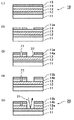
この、EUVリソグラフィーに用いる反射型マスクの製造方法を図4を参照しながら説明する。図4は、従来の反射型マスクの製造工程を表わす断面の概略図である。
(1)SiO2基板11上に、順次EUV多層反射膜である積層膜12、その上に吸収体パターン形成工程におけるEUV 層の保護を目的としてバッファー層13、その上にEUV 吸収体である吸収体層14 を成膜する。その後、この吸収体層表面に有機レジスト膜16 を塗布する(図4(1))。
(2)有機レジスト膜16に、レジストパターン16a を形成する(図4(2))。
(3)このレジストパターン16a により吸収体層14をエッチング加工し所定のパターンを有する 吸収体パターン14a を形成する。ここで、形成された吸収体パターン14a の検査を実施する(図4(3))。具体的には、エッチング除去されるべきでない箇所の吸収体層が除去されたピンホール欠陥21(白欠陥ともいう)や、エッチング不足により吸収体層が十分に除去されていない箇所22(黒欠陥ともいう)を検出する。
(4)吸収体パターン14aの欠陥を修正し、修正された吸収体パターン14b とする(図4(4))。
(5)最後にバッファー層13 のパターン13a形成を実施し、EUV反射型マスクとなる。これにEUV光31を照射すると、吸収体層14およびバッファー層13を除去して反射積層膜12が露出した部分のみEUV 光31 を反射し、リソグラフィーに使用することができる(図4(5))
A method of manufacturing the reflective mask used in EUV lithography will be described with reference to FIG. FIG. 4 is a schematic cross-sectional view showing a manufacturing process of a conventional reflective mask.
(1) A laminated
(2) A
(3) The
(4) The defect of the
(5) Finally, the
上述のEUV 反射型マスク作成工程において、(3)の吸収体パターンの検査では、波長193nm から257 nm の遠紫外光を使用した反射型の検査機が使用される。検査は、この検査光をパターンが形成された反射型マスクの表面に入射し、マスク表面での検査光の反射のコントラストを観察することにより行われる。
又、(5)のバッファ層の除去後、仕様通りの吸収体パターンが形成されているかどうか最終確認の検査が行われる。このパターンの最終検査も、上述した検査同様、遠紫外光を検査光としてマスク表面での検査光の反射光のコントラストを観察する事によって行われる。
In addition, after the removal of the buffer layer in (5), a final check is performed to determine whether the absorber pattern according to the specification is formed. Similar to the above-described inspection, the final inspection of this pattern is performed by observing the contrast of the reflected light of the inspection light on the mask surface using far ultraviolet light as inspection light.
上述した吸収体層への転写パターンの形成においては、有機物質からなるレジストを使用するが、このようなレジストは一般にドライエッチング耐性が低く、吸収体層のパターン形成時にレジスト膜が損傷を受けるため、レジスト層は、ある一定以上の膜厚(通常500nmから800nm程度)が必要であった。
ところが、マスクに要求されるパターンの線幅が細くなると、このような厚いレジストに細いパターンを形成するのは、次の点で困難になってきた。
すなわち、第一にレジストの垂直方向の形状精度が取り難く、吸収体パターンの形状精度が悪化する。第二にエッチングガスがレジストパターンの細い通路に供給されにくく、又、エッチングにより発生したガスも滞留しやすいため、線幅の狭い部分でエッチングの反応が進みにくい。従って、線幅の広い部分と、狭い部分でのエッチング速度に差が出てしまい、マスク面内で均一なエッチングが行えない。
このような点から、従来の厚いレジストを使用すると、例えば、解像度0.1μm以下というような線幅の細いパターンの形成が困難であるという問題があった。
In forming the transfer pattern on the absorber layer described above, a resist made of an organic material is used. However, such a resist generally has low dry etching resistance, and the resist film is damaged when the absorber layer pattern is formed. The resist layer needs to have a certain thickness (usually about 500 nm to 800 nm).
However, when the line width of the pattern required for the mask is reduced, it has become difficult to form a thin pattern on such a thick resist in the following points.
That is, first, it is difficult to obtain the shape accuracy of the resist in the vertical direction, and the shape accuracy of the absorber pattern is deteriorated. Secondly, the etching gas is difficult to be supplied to the narrow passage of the resist pattern, and the gas generated by the etching is likely to stay, so that the etching reaction is difficult to proceed in a portion having a narrow line width. Therefore, there is a difference in etching rate between a wide line width portion and a narrow portion, and uniform etching cannot be performed within the mask surface.
From such a point, when a conventional thick resist is used, there is a problem that it is difficult to form a pattern having a thin line width such as a resolution of 0.1 μm or less.
一方、上述した吸収体層のパターンの検査においては、吸収体層が除去された部分に露出したバッファ層表面或いは、バッファ層が除去されて露出した多層反射膜表面と、吸収体層が残っている部分の吸収体層表面の間で上述した検査光による検査がなされることになる。
そのため、検査光の波長に対するバッファ層表面或いは多層反射膜表面と吸収体層表面との反射率の差が小さいと、検査時のコントラストが悪くなり、正確な検査が行えないという問題があった。
そこで、本発明は上述の課題を解決するために案出されたものであり、吸収体層に微細なパターンを形状精度よく形成でき、パターン検査において十分なコントラストが得られ、高精度のパターン転写が可能な反射型マスク及び反射型マスクブランクスを得る事を目的としたものである。
On the other hand, in the inspection of the pattern of the absorber layer described above, the surface of the buffer layer exposed at the portion where the absorber layer is removed or the surface of the multilayer reflective film exposed by removing the buffer layer and the absorber layer remain. The inspection with the above-described inspection light is performed between the surfaces of the absorber layer in the existing portions.
Therefore, if the difference in reflectance between the buffer layer surface or the multilayer reflective film surface and the absorber layer surface with respect to the wavelength of the inspection light is small, there is a problem that the contrast at the time of inspection deteriorates and accurate inspection cannot be performed.
Therefore, the present invention has been devised to solve the above-mentioned problems, and can form a fine pattern on the absorber layer with high shape accuracy, provide sufficient contrast in pattern inspection, and provide high-accuracy pattern transfer. The object of the present invention is to obtain a reflective mask and a reflective mask blank that can be used.
本出願人は、上記パターン検査時のコントラストの課題に対し、吸収体層を積層構造とし、その最上層をパターン検査に使用する光に対して反射率の低い材料からなる低反射層とする構成の反射型マスク及び反射型マスクブランクスを先に提案した(特願2002−108808)。
本発明者らは、この反射型マスクを更に改良し、上記低反射層に所定の特性を有する材料を使用することにより、低反射層に、それより下層の吸収体層にパターン形成をする際の無機エッチングマスク層の機能を兼ね備えることができることを見出した。そして、低反射層を薄い無機エッチングマスク層として機能させることにより、上記課題が解決できることを見出した。
The applicant has a configuration in which the absorber layer has a laminated structure and the uppermost layer is a low-reflective layer made of a material having low reflectivity with respect to light used for pattern inspection, in order to solve the above-described contrast problem during pattern inspection. Previously proposed a reflective mask and a reflective mask blank (Japanese Patent Application No. 2002-108808).
The inventors of the present invention have further improved the reflective mask and used a material having predetermined characteristics for the low reflective layer to form a pattern on the low reflective layer and the absorber layer below it. It has been found that the inorganic etching mask layer can be provided with the function of the above. And it discovered that the said subject could be solved by making a low reflective layer function as a thin inorganic etching mask layer.
すなわち、本発明の反射型マスクブランクスは、基板と、該基板上に順次形成された、露光光を反射する多層反射膜及び露光光を吸収する吸収体層を備えた反射型マスクブランクスであって、前記吸収体層は、少なくとも最上層と、それ以外の下層とからなる積層構造となっており、前記最上層は、前記吸収体層に形成された吸収体層のパターンの検査に使用する検査波長の光に対する反射率が20%以下であり、かつ下層へのパターン形成の際のエッチング条件に対し耐性を有する無機材料で形成されていることを特徴とする。
また、本発明の反射型マスクブランクスは、基板と、基板上に順次形成された、露光光を反射する多層反射膜及び露光光を吸収する吸収体層を備えた反射型マスクブランクスであって、前記吸収体層は、少なくとも最上層と、それ以外の下層とからなる積層構造となっており、前記最上層は、前記吸収体層に形成された吸収体層のパターンの検査に使用する検査波長の光において、前記吸収体層の直下の層に対する下記の式で示されるコントラスト値が40%以上であり、かつ下層へのパターン形成の際のエッチング条件に対し耐性を有する無機材料で形成されていることを特徴とする。
(式)コントラスト値(%)=(R2−R1)/(R2+R1)×100
(ただし、R1は検査波長の光に対する最上層表面の反射率、R2は吸収体層直下の層表面の反射率)
That is, the reflective mask blank of the present invention is a reflective mask blank that includes a substrate, a multilayer reflective film that reflects exposure light, and an absorber layer that absorbs exposure light, which are sequentially formed on the substrate. The absorber layer has a laminated structure including at least an uppermost layer and other lower layers, and the uppermost layer is an inspection used for inspecting a pattern of the absorber layer formed on the absorber layer. It is characterized by being formed of an inorganic material having a reflectance with respect to light of a wavelength of 20% or less and having resistance to etching conditions when forming a pattern in the lower layer.
Moreover, the reflective mask blank of the present invention is a reflective mask blank including a substrate, a multilayer reflective film that reflects exposure light, and an absorber layer that absorbs exposure light, which are sequentially formed on the substrate, The absorber layer has a laminated structure composed of at least an uppermost layer and other lower layers, and the uppermost layer is an inspection wavelength used for inspecting the pattern of the absorber layer formed on the absorber layer. In contrast, the contrast value expressed by the following formula with respect to the layer immediately below the absorber layer is 40% or more, and is formed of an inorganic material having resistance to etching conditions when forming a pattern in the lower layer. It is characterized by being.
(Formula) Contrast value (%) = (R 2 −R 1 ) / (R 2 + R 1 ) × 100
(Where R 1 is the reflectance of the surface of the uppermost layer with respect to light of the inspection wavelength, and R 2 is the reflectance of the surface of the layer immediately below the absorber layer)
前記吸収体層のパターンの検査には波長が190nm〜260nmの範囲に含まれる検査光が使用される。
前記吸収体層の下層にパターンを形成する際の前記最上層と下層とのエッチング選択比が5以上であることが望ましい。
前記吸収体層の具体的材料としては、例えば、前記吸収体層の下層がタンタル(Ta)を含む材料で、前記最上層がケイ素(Si)を含む材料でそれぞれ構成することができる。
また、前記多層反射膜と吸収体層との間に、更に、吸収体層の下層のパターン形成及びパターン修正の際のエッチング条件に対し耐性を有するバッファ層を設けてもよい。このバッファ層は例えばクロム(Cr)を含む材料で構成することができる。
本発明の反射型マスクは、以上のような反射型マスクブランクスの吸収体層にパターンを形成したものである。
本発明の反射型マスクは、まず積層構造からなる吸収体層の最上層にパターンを形成し、次いで該最上層に形成されたパターンをマスクとして吸収体層の下層のエッチングを行い、下層にパターンを形成することにより製造することができる。
また、前記多層反射膜と吸収体層との間に、更にバッファ層を設けた場合は、前記吸収体層の最上層及び下層にパターンを形成した後、該吸収体層に形成されたパターンをマスクとしてバッファ層のエッチングを行い、バッファ層にパターンを形成する。
For the inspection of the pattern of the absorber layer, inspection light having a wavelength in the range of 190 nm to 260 nm is used.
It is desirable that the etching selectivity between the uppermost layer and the lower layer when forming a pattern in the lower layer of the absorber layer is 5 or more.
As a specific material of the absorber layer, for example, the lower layer of the absorber layer can be made of a material containing tantalum (Ta) and the uppermost layer can be made of a material containing silicon (Si).
In addition, a buffer layer having resistance to etching conditions for pattern formation and pattern correction in the lower layer of the absorber layer may be provided between the multilayer reflective film and the absorber layer. This buffer layer can be made of, for example, a material containing chromium (Cr).
The reflective mask of the present invention is obtained by forming a pattern on the absorber layer of the reflective mask blank as described above.
In the reflective mask of the present invention, a pattern is first formed in the uppermost layer of the absorber layer having a laminated structure, and then the lower layer of the absorber layer is etched using the pattern formed in the uppermost layer as a mask. Can be manufactured.
Further, when a buffer layer is further provided between the multilayer reflective film and the absorber layer, after forming a pattern on the uppermost layer and the lower layer of the absorber layer, the pattern formed on the absorber layer Etching the buffer layer as a mask forms a pattern in the buffer layer.
以下に、本発明の反射型マスクブランクス及び反射型マスクの実施の形態について説明する。本発明の反射型マスクブランクス及び反射型マスクは、基板上に順次、多層反射膜、吸収体層の各層が形成された構造で、前記吸収体層は積層構造になっている。又、多層反射膜と吸収体層の間に吸収体層のパターン形成及びパターン修正の際のエッチング条件に耐性を有するバッファ層を有していても良い。
ここで、本発明の反射型マスクブランクス及び反射型マスクを形成する各層について説明する。
Hereinafter, embodiments of the reflective mask blank and the reflective mask of the present invention will be described. The reflective mask blank and the reflective mask of the present invention have a structure in which a multilayer reflective film and an absorber layer are sequentially formed on a substrate, and the absorber layer has a laminated structure. Moreover, you may have the buffer layer which has tolerance to the etching conditions at the time of pattern formation and pattern correction of an absorber layer between a multilayer reflective film and an absorber layer.
Here, each layer forming the reflective mask blank and the reflective mask of the present invention will be described.
まず、吸収体層について説明する。
本発明の反射型マスクブランクス及び反射型マスクの吸収体層は、露光光であるEUV光を吸収する機能を有する。本発明の吸収体層は、最上層と、それ以外の下層からなる積層構造になっている。下層は更に、複数の層からなっていても良いが、最上層と、一層の下層からなる2層構造とするのが、製造工程・材料の種類が少なくてすむために好ましい。
まず、最上層について説明する。
本発明の最上層は、吸収体層に形成された吸収体パターンの検査において低反射層として機能すると共に、吸収体下層にパターンを形成する際のエッチングマスクとして機能する。
本発明の最上層は、まず、吸収体パターンの検査時において、吸収体層の直下に形成される層(通常は後述するバッファ層或いは多層反射膜)との間で、十分なコントラストが取れる材料から選択される。検査における吸収体層の直下にある層とのコントラスト値は、40%以上、好ましくは60%以上となるようにするのがよい。
なお、検査時のコントラスト値は次の式で定義される。
コントラスト値(%)=(R2−R1)/(R2+R1)×100
(ただし、R1,R2は検査を行う各層における反射率で、R2>R1)
First, the absorber layer will be described.
The reflective mask blank of the present invention and the absorber layer of the reflective mask have a function of absorbing EUV light that is exposure light. The absorber layer of the present invention has a laminated structure composed of an uppermost layer and other lower layers. The lower layer may further consist of a plurality of layers, but a two-layer structure consisting of the uppermost layer and one lower layer is preferable because the number of manufacturing steps and materials can be reduced.
First, the top layer will be described.
The uppermost layer of the present invention functions as a low reflection layer in the inspection of the absorber pattern formed in the absorber layer and also functions as an etching mask when forming a pattern in the absorber lower layer.
The uppermost layer of the present invention is a material that can provide sufficient contrast with a layer (usually a buffer layer or a multilayer reflective film, which will be described later) formed immediately below the absorber layer at the time of inspection of the absorber pattern. Selected from. The contrast value with the layer immediately below the absorber layer in the inspection should be 40% or more, preferably 60% or more.
The contrast value at the time of inspection is defined by the following equation.
Contrast value (%) = (R 2 −R 1 ) / (R 2 + R 1 ) × 100
(However, R 1 and R 2 are reflectivities in each layer to be inspected, and R 2 > R 1 )
例えば、波長257nmの光を検査光とした場合、一般にバッファ層として用いられる物質の反射率は、SiO2で40%程度、Crで50%程度である。又、波長13nm付近の露光光に対して一般に用いられるMo/Si周期多層膜からなる多層反射膜の遠紫外光に対する反射率は60%程度である。このように、一般的に使用されるバッファ層、多層反射膜の検査波長に対する反射率は比較的大きいため、最上層の材料は、検査波長に対し、反射率の小さい材料を使用するのが上記十分なコントラストを得る上で有利である。
このような点から、吸収体層の最上層の検査波長に対する反射率は、20%以下とするのが好ましく、10%以下とするのが更に好ましい。
本発明の最上層は、更に、上述した検査光に対する反射率の条件を満たす材料のうち、吸収体層の下層にパターンを形成する際のエッチング条件に対し、耐性を持った無機材料が選択される。
従来の有機物質を用いたレジストに対し、無機材料を用いたエッチングマスクは、ドライエッチング耐性に優れているため、薄く形成することが可能になる。従って、線幅が細いパターンであっても、形状精度よく吸収体層にパターンを形成することができる。
For example, when light having a wavelength of 257 nm is used as inspection light, the reflectance of a substance generally used as a buffer layer is about 40% for SiO 2 and about 50% for Cr. Further, the reflectance of the multilayer reflective film made of a Mo / Si periodic multilayer film generally used for exposure light having a wavelength of around 13 nm with respect to far ultraviolet light is about 60%. As described above, since the reflectance of the buffer layer and the multilayer reflective film that are generally used is relatively large with respect to the inspection wavelength, the material of the uppermost layer should be a material having a low reflectance with respect to the inspection wavelength. This is advantageous for obtaining sufficient contrast.
From such a point, the reflectance of the absorber layer with respect to the inspection wavelength is preferably 20% or less, and more preferably 10% or less.
For the uppermost layer of the present invention, an inorganic material that is resistant to the etching conditions for forming a pattern in the lower layer of the absorber layer is selected from among the materials that satisfy the above-described reflectance requirements for the inspection light. The
An etching mask using an inorganic material is superior in dry etching resistance to a conventional resist using an organic substance, and thus can be formed thin. Therefore, even if the line width is a thin pattern, the pattern can be formed on the absorber layer with good shape accuracy.
最上層と下層とのエッチング選択比は、好ましくは5以上、更に好ましくは10以上である。エッチング選択比が大きいほど、最上層を薄くできる。ただし、最上層が薄すぎると検査波長に対する反射率が高くなるので、上述した検査波長に対する反射率を確保するため、通常、最上層は、15〜30nm程度の厚さに形成される。
このように、本発明の吸収体層の最上層は検査波長に対し低反射率を有し、かつ、下層にパターンを形成する際のエッチングマスク層の機能も有するため、簡単な層構造で、検査時のコントラストが十分得られるとともに、線幅の細い吸収体パターンが精度よく形成できる反射型マスク及び反射型マスクブランクスが得られる。又、多層反射膜と吸収体層の間にバッファ層を有する場合には、最上層は、バッファ層にパターンを形成する際のマスクとしても用いることができる。
The etching selectivity between the uppermost layer and the lower layer is preferably 5 or more, more preferably 10 or more. The higher the etching selectivity, the thinner the top layer. However, if the uppermost layer is too thin, the reflectance with respect to the inspection wavelength is increased. Therefore, in order to ensure the reflectance with respect to the inspection wavelength described above, the uppermost layer is usually formed with a thickness of about 15 to 30 nm.
Thus, since the uppermost layer of the absorber layer of the present invention has a low reflectance with respect to the inspection wavelength and also has a function of an etching mask layer when forming a pattern in the lower layer, it has a simple layer structure, A reflection mask and a reflection mask blank can be obtained in which sufficient contrast at the time of inspection can be obtained and an absorber pattern with a narrow line width can be formed with high accuracy. When a buffer layer is provided between the multilayer reflective film and the absorber layer, the uppermost layer can also be used as a mask when forming a pattern on the buffer layer.
次に、吸収体層の下層について説明する。下層は、主に、露光光であるEUV光の吸収機能を担う。従って、EUV光の吸収の大きい物質を用いる。このような吸収体層の下層としては、EUV光に対する吸収係数が大きく加工性に優れている点から、タンタルを含む材料、例えばタンタルやタンタル合金が好ましく用いられる。
このような材料の具体例として、タンタル単体、タンタルホウ素合金(TaB),タンタルホウ素合金の窒化物(TaBN)、タンタルゲルマニウム合金(TaGe),タンタルゲルマニウム合金の窒化物(TaGeN),タンタルシリコン合金(TaSi),タンタルシリコン合金の窒化物(TaSiN)、タンタルシリコンホウ素合金(TaSiB),タンタルゲルマニウムホウ素合金(TaGeB)、タンタルシリコンホウ素合金の窒化物(TaSiBN),タンタルゲルマニウムホウ素合金の窒化物(TaGeBN)等が挙げられる。また、これらに更に、炭素や酸素を含んでいても良い。
本発明の下層の膜構造は、経時変化への安定性、耐環境性の点から微結晶(粒径数nm以下)もしくはアモルファスであるのが好ましい。 タンタルとホウ素を含む合金は、アモルファス化が容易で、平滑性に優れた膜が得られるという利点を有する。また、膜応力の制御性にも優れているため、マスクパターンの寸法精度を高精度に形成できる点で好ましい。この場合、アモルファス化のために好ましいホウ素の含有量は、10〜25at%である。タンタルとホウ素の合金に窒素を含んだ物質も好ましく用いられる。窒素を加えることで膜の平滑性を向上させ、表面粗さを小さくする効果が得られる。
又、本発明の吸収体層下層には、タンタルを含む材料以外には、クロム、マンガン、ガリウム、ハフニウム、タングステンを含む材料、例えばこれらの単体又はこれらの元素を含む合金等を用いることができる。
Next, the lower layer of the absorber layer will be described. The lower layer mainly has a function of absorbing EUV light that is exposure light. Therefore, a substance having a large EUV light absorption is used. As the lower layer of such an absorber layer, a material containing tantalum such as tantalum or a tantalum alloy is preferably used because it has a large absorption coefficient for EUV light and is excellent in workability.
Specific examples of such materials include tantalum alone, tantalum boron alloy (TaB), tantalum boron alloy nitride (TaBN), tantalum germanium alloy (TaGe), tantalum germanium alloy nitride (TaGeN), and tantalum silicon alloy ( TaSi), tantalum silicon alloy nitride (TaSiN), tantalum silicon boron alloy (TaSiB), tantalum germanium boron alloy (TaGeB), tantalum silicon boron alloy nitride (TaSiBN), tantalum germanium boron alloy nitride (TaGeBN) Etc. Further, these may further contain carbon or oxygen.
The lower layer film structure of the present invention is preferably microcrystalline (particle size of several nm or less) or amorphous from the viewpoint of stability over time and environmental resistance. An alloy containing tantalum and boron has an advantage that a film excellent in smoothness can be obtained because it can be easily amorphized. Moreover, since the controllability of the film stress is excellent, it is preferable in that the dimensional accuracy of the mask pattern can be formed with high accuracy. In this case, the preferable boron content for amorphization is 10 to 25 at%. A substance containing nitrogen in an alloy of tantalum and boron is also preferably used. By adding nitrogen, it is possible to improve the smoothness of the film and reduce the surface roughness.
In addition to the material containing tantalum, a material containing chromium, manganese, gallium, hafnium, tungsten, for example, a simple substance of these or an alloy containing these elements can be used for the lower layer of the absorber layer of the present invention. .
反射型マスクにおいては、露光光はマスク面に対し垂直な方向から数度傾いた方向より入射される。従って、吸収体パターンの厚みが厚いと、パターン自身の影が生じ、露光時にパターンのエッジ部分にぼやけなどが生じて鮮明な転写像が得られないため、吸収体層全体の厚みは、薄い方が好ましい。この点から、吸収体層の下層は、露光光の波長に対し、吸収係数が大きい方が有利であり、0.025以上、更には、0.030以上であるのであるのが好ましい。なお、吸収体層全体の膜厚は、露光光であるEUV光が十分に吸収できる厚みでなるべく薄い方が良いが、通常30〜100nm程度である。更に好ましくは80nm以下である。
又、吸収体層全体を薄くするという目的のためには、最上層のEUV吸収率が高いほうが有利である。最上層のEUV吸収能が大きいほど、その分下層を薄く出来るからである。最上層の材料の好ましいEUV吸収係数は、0.01以上、好ましくは0.015以上である。
上述したように、本発明では、吸収体層を最上層と下層で機能を分離して積層構造としたことにより、各層それぞれの特性を最適化でき、結果として、吸収体層の厚みを小さくできるという利点も有する。
吸収体層(最上層及び下層)は、マグネトロンスパッタリングなどのスパッタ法等一般的な成膜方法で製造できる。例えば、タンタルホウ素合金の窒化物(TaBN)であれば、タンタルとホウ素を含む合金ターゲットを用い、窒素を添加したアルゴンガスを用いた反応性DCスパッタリング法で成膜することができる。
In the reflective mask, the exposure light is incident from a direction inclined several degrees from the direction perpendicular to the mask surface. Therefore, if the thickness of the absorber pattern is thick, the shadow of the pattern itself will be generated, and the edge of the pattern will be blurred during exposure and a clear transfer image cannot be obtained. Is preferred. From this point, it is advantageous that the lower layer of the absorber layer has a larger absorption coefficient with respect to the wavelength of exposure light, and is preferably 0.025 or more, more preferably 0.030 or more. The film thickness of the entire absorber layer is preferably as thin as possible so that EUV light as exposure light can be sufficiently absorbed, but is usually about 30 to 100 nm. More preferably, it is 80 nm or less.
For the purpose of thinning the entire absorber layer, it is advantageous that the EUV absorption rate of the uppermost layer is high. This is because the lower the EUV absorption capacity of the uppermost layer, the thinner the lower layer. A preferable EUV absorption coefficient of the uppermost layer material is 0.01 or more, preferably 0.015 or more.
As described above, in the present invention, the function of the absorber layer is separated into the uppermost layer and the lower layer to form a laminated structure, whereby the characteristics of each layer can be optimized, and as a result, the thickness of the absorber layer can be reduced. It also has the advantage of.
The absorber layer (the uppermost layer and the lower layer) can be manufactured by a general film forming method such as a sputtering method such as magnetron sputtering. For example, a nitride of tantalum boron alloy (TaBN) can be formed by a reactive DC sputtering method using an alloy target containing tantalum and boron and using an argon gas to which nitrogen is added.
次に、バッファ層について説明する。
バッファ層は、吸収体層にパターンを形成及びパターンを修正する際に、多層反射膜を保護する機能を有する。そのため、本発明のバッファ層は、吸収体層下層のパターン形成時のエッチング条件に耐性を有する材料が選択される。
例えばTaを含む吸収体層下層材料と組み合わせるバッファ層としては、Crを含む材料からなるバッファ層が好ましく用いられる。Crを含む材料からなるバッファ層は、Taを含む本発明の吸収体層とのエッチング選択比が大きく取れる(20以上)。又、Crを含む材料は、検査波長における反射率が約40%〜55%程度であり、後述する多層反射膜表面、バッファ層表面、吸収体層表面の検査波長における反射率の関係からも好ましい。更には、バッファ層除去時に多層反射膜へのダメージをほとんど与えずに除去できる。
バッファ層として用いられるCrを含む材料しては、Cr単体以外に、CrとN,O,Cから選択される少なくとも一つの元素を含む材料を好ましく用いることができる。例えば、窒化クロム(CrN)、酸化クロム(CrO)、炭化クロム(CrC)、酸化窒化クロム(CrNO)、炭化窒化酸化クロム(CrCNO)等である。
Crを含むバッファ層は、マグネトロンスパッタ法などのスパッタ法で形成することができる。例えば、上述した窒化クロム膜の場合、Crターゲットを用い、Arに窒素を5〜40%程度添加したガス雰囲気で成膜を行えばよい。
Next, the buffer layer will be described.
The buffer layer has a function of protecting the multilayer reflective film when forming a pattern on the absorber layer and modifying the pattern. Therefore, for the buffer layer of the present invention, a material having resistance to the etching conditions at the time of pattern formation of the absorber layer lower layer is selected.
For example, as the buffer layer combined with the absorber layer lower layer material containing Ta, a buffer layer made of a material containing Cr is preferably used. The buffer layer made of a material containing Cr can have a large etching selectivity with respect to the absorber layer of the present invention containing Ta (20 or more). In addition, the Cr-containing material has a reflectance of about 40% to 55% at the inspection wavelength, which is preferable from the relationship of the reflectance at the inspection wavelength of the multilayer reflective film surface, the buffer layer surface, and the absorber layer surface described later. . Furthermore, it can be removed with little damage to the multilayer reflective film when removing the buffer layer.
As the material containing Cr used as the buffer layer, a material containing at least one element selected from Cr and N, O, and C can be preferably used in addition to Cr alone. Examples thereof include chromium nitride (CrN), chromium oxide (CrO), chromium carbide (CrC), chromium oxynitride (CrNO), and carbon nitride nitride oxide (CrCNO).
The buffer layer containing Cr can be formed by a sputtering method such as a magnetron sputtering method. For example, in the case of the chromium nitride film described above, film formation may be performed in a gas atmosphere using a Cr target and adding about 5 to 40% of nitrogen to Ar.
バッファ層の膜厚は、集束イオンビーム(Focused Ion Beam,FIB)を用いた吸収体パターンの修正を行う場合には、30〜50nmとするのが好ましいが、FIBを用いない場合には、4〜10nmと薄くすることができる。
その他に、本発明の吸収体層と組み合わせて使用できるバッファ層としては、SiO2,シリコンの酸化窒化物(SiON)、Ru等が挙げられ、Taを含まない吸収体層との組み合わせではTaをバッファ層として使用することもできる。
本発明では、吸収体層の最上層に下層へのパターン形成の際のエッチングマスクとしての機能を実現させるために、最上層及び下層の材料の組み合わせが重要である。更に、バッファ層を有する場合にはバッファ層と各層との組み合わせも重要である。
The thickness of the buffer layer is preferably 30 to 50 nm when the absorber pattern is corrected using a focused ion beam (FIB), but is 4 when the FIB is not used. It can be as thin as -10 nm.
In addition, examples of the buffer layer that can be used in combination with the absorber layer of the present invention include SiO 2 , silicon oxynitride (SiON), Ru, and the like, and Ta in combination with an absorber layer not containing Ta. It can also be used as a buffer layer.
In the present invention, the combination of the materials of the uppermost layer and the lower layer is important in order to realize the function as an etching mask when forming the pattern on the lower layer on the uppermost layer of the absorber layer. Further, when a buffer layer is provided, the combination of the buffer layer and each layer is also important.
以下、各層の材料の選択につき説明する。
まず、バッファ層がない場合には、最上層に求められる最低条件は、吸収体パターンの検査光に対して低反射率を有すること、吸収体層の下層のエッチング条件に耐性を有すること、及び最上層へのマスクパターン形成時のエッチング条件において下層がエッチングされない(下層が最上層のエッチング条件に耐性を有する)ことである。従って、まず、吸収体層の最上層と下層は、全く異なるエッチング特性を有しているものが好ましい。吸収体層の下層として、例えばTaを含む材料を使用した場合には、通常、塩素ガスを用いたドライエッチングでパターン形成されるため、最上層は、塩素エッチングに対して耐性を有する材料であり、かつTaを含む材料が耐性を有しているエッチング条件でエッチングが可能である材料から選択される。このような材料としては、例えば、Siを含む材料、Crを含む材料が挙げられる。このような材料のうち、吸収体層のパターン検査に用いる検査波長の光に対し、十分低い反射率を有する材料が選択され、例えば、SiON、金属とシリコンの合金の酸窒化物(例えばMoSiON)、クロムの酸化物(CrO),クロムの酸窒化物(CrON)等が用いられる。
また、吸収体層の下層として、Crを含む材料を使用した場合には、通常、塩素と酸素の混合ガスを用いたドライエッチングでパターン形成されるため、最上層は、塩素と酸素の混合ガスのエッチングに対して耐性を有する材料であり、かつCrを含む材料が耐性を有しているエッチング条件でエッチングが可能である材料から選択される。このような材料としては、例えば、Siを含む材料、Taを含む材料が挙げられる。このような材料のうち、吸収体層のパターン検査に用いる検査波長の光に対し、十分低い反射率を有する材料が選択され、例えば、SiON、金属とシリコンの合金の酸窒化物(例えばMoSiON)、タンタルの酸化物(TaO),タンタルの酸窒化物(TaON)、タンタルホウ素合金の酸化物(TaBO),タンタルホウ素合金の酸窒化物(TaBNO)、タンタルとシリコンの酸窒化物(TaSiON)等が用いられる。
Hereinafter, selection of materials for each layer will be described.
First, when there is no buffer layer, the minimum conditions required for the uppermost layer are to have a low reflectance with respect to the inspection light of the absorber pattern, to have resistance to etching conditions under the absorber layer, and The lower layer is not etched under the etching conditions when forming the mask pattern on the uppermost layer (the lower layer is resistant to the etching conditions of the uppermost layer). Therefore, first, it is preferable that the uppermost layer and the lower layer of the absorber layer have completely different etching characteristics. For example, when a material containing Ta is used as the lower layer of the absorber layer, since the pattern is usually formed by dry etching using chlorine gas, the uppermost layer is a material having resistance to chlorine etching. And a material containing Ta is selected from materials that can be etched under etching conditions with resistance. Examples of such a material include a material containing Si and a material containing Cr. Among these materials, a material having a sufficiently low reflectance with respect to light having an inspection wavelength used for pattern inspection of the absorber layer is selected. For example, SiON, metal-silicon alloy oxynitride (for example, MoSiON) Further, chromium oxide (CrO), chromium oxynitride (CrON), or the like is used.
In addition, when a material containing Cr is used as the lower layer of the absorber layer, it is usually patterned by dry etching using a mixed gas of chlorine and oxygen, so the uppermost layer is a mixed gas of chlorine and oxygen. It is selected from materials that are resistant to etching and that can be etched under etching conditions in which a material containing Cr has resistance. Examples of such a material include a material containing Si and a material containing Ta. Among these materials, a material having a sufficiently low reflectance with respect to light having an inspection wavelength used for pattern inspection of the absorber layer is selected. For example, SiON, metal-silicon alloy oxynitride (for example, MoSiON) Tantalum oxide (TaO), tantalum oxynitride (TaON), tantalum boron alloy oxide (TaBO), tantalum boron alloy oxynitride (TaBNO), tantalum and silicon oxynitride (TaSiON), etc. Is used.
このように最上層として、金属又は合金(例えば、Siとの合金やBとの合金)の酸化物、窒化物、酸窒化物等が好ましく用いられる。最上層の材料は、上述した吸収体層下層とのエッチングの関係が満たされるよう、吸収体下層の材料との関係で選択すればよい。このうち、金属の酸化物、窒化物の場合、一般に、窒素又は酸素の量が多くなるほど、検査波長に対する反射率は低下するため、酸素又は窒素の量を調整することで、最上層の検査波長に対する反射率をある程度コントロールすることができる。又、金属とシリコンの合金の酸窒化物は、反射率が低い検査光の波長帯域が比較的広く、検査光の変更にも柔軟に対応できる点、膜厚の差による反射率の変化が小さい点で好ましい。
また、多層反射膜と吸収体層の間にバッファ層がある場合には、最上層には前述の条件のほかに、更に次の特性が求められる。すなわち、バッファ層にパターンを形成する際のエッチング条件に耐性を有することである。例えば、バッファ層にCrを含む材料を使用した場合、一般に、そのエッチングには、酸素と塩素を含むガスが用いられる。従って、吸収体層の最上層は、酸素と塩素の混合ガスに対する耐性を有する必要がある。このような材料としては例えば、Siを含む材料(金属とシリコンの合金の酸窒化物)、Zrを含む材料,Taを含む材料,Tiを含む材料等が挙げられる。具体的には、TaとZrの合金(TaZr),TaとZrの合金の窒化物(TaZrN),窒化チタン(TiN)やこれらの酸化物等が挙げられる。
As described above, an oxide, nitride, oxynitride or the like of a metal or an alloy (for example, an alloy with Si or an alloy with B) is preferably used as the uppermost layer. The material of the uppermost layer may be selected in relation to the material of the absorber lower layer so that the above-described etching relationship with the absorber layer lower layer is satisfied. Of these, in the case of metal oxides and nitrides, the reflectivity with respect to the inspection wavelength generally decreases as the amount of nitrogen or oxygen increases, so the inspection wavelength of the uppermost layer can be adjusted by adjusting the amount of oxygen or nitrogen. The reflectance with respect to can be controlled to some extent. In addition, the metal-silicon alloy oxynitride has a relatively wide inspection light wavelength band with a low reflectivity, and can flexibly respond to changes in the inspection light, and the change in reflectivity due to the difference in film thickness is small. This is preferable.
In addition, when there is a buffer layer between the multilayer reflective film and the absorber layer, the uppermost layer is required to have the following characteristics in addition to the aforementioned conditions. That is, it has resistance to etching conditions when forming a pattern in the buffer layer. For example, when a material containing Cr is used for the buffer layer, a gas containing oxygen and chlorine is generally used for the etching. Therefore, the uppermost layer of the absorber layer needs to have resistance to a mixed gas of oxygen and chlorine. Examples of such a material include a material containing Si (oxynitride of an alloy of metal and silicon), a material containing Zr, a material containing Ta, a material containing Ti, and the like. Specifically, an alloy of Ta and Zr (TaZr), a nitride of an alloy of Ta and Zr (TaZrN), titanium nitride (TiN), or an oxide thereof can be used.
一方、バッファ層にSiO2を用いた場合には、バッファ層のエッチングには、SF6や、フッ化炭素(CF4,C2F6)などのフッ素系ガスが使用される。従って、この場合最上層には、フッ素系ガスに対する耐性を有するものを選択する。このような材料としては、Crを含む材料、Tiを含む材料、Zrを含む材料等が挙げられる。具体的には、窒化チタン(TiN),窒化ジルコニウム(ZrN)やその酸化物等が挙げられる。
これら最上層の材料は、もちろん吸収体層下層の材料との関係も考慮する必要があるため、吸収体層下層の材料に応じて、前述した吸収体層下層の材料とのエッチングの関係により、適宜選択すればよい。
以上のように、各層の材料は、吸収体層の最上層及び下層、並びにバッファ層へのパターン形成時のエッチング条件及びエッチング選択比を考慮し、かつ、パターン検査波長において十分なコントラストが得られるように、各層の組み合わせを決定すればよい。
各層の材料の好ましい組み合わせとしては、例えば、吸収体層下層としてTaを含む材料(塩素ガスでエッチング可能)、最上層としてSiを含む材料(フッ素系ガスでエッチング可能)、バッファ層としてCrを含む材料(塩素+酸素ガスでエッチング可能)である。又、吸収体層下層としてCrを含む材料(酸素+塩素でエッチング可能)、最上層としてSiを含む材料(フッ素系ガスでエッチング可能)、バッファ層としてTaを含む材料(塩素ガスでエッチング可能)も好ましい。
又、上記条件を満たすように材料を選択できるのであれば、エッチング処理においては、ドライエッチングのみならず、ウエットエッチングを用いても良い。
On the other hand, when SiO 2 is used for the buffer layer, a fluorine-based gas such as SF 6 or fluorocarbon (CF 4 , C 2 F 6 ) is used for etching the buffer layer. Therefore, in this case, the uppermost layer is selected to have resistance to fluorine-based gas. Examples of such a material include a material containing Cr, a material containing Ti, and a material containing Zr. Specific examples include titanium nitride (TiN), zirconium nitride (ZrN), and oxides thereof.
Since these top layer materials need to consider the relationship with the material of the absorber layer lower layer, of course, depending on the material of the absorber layer lower layer, depending on the etching relationship with the material of the absorber layer lower layer, What is necessary is just to select suitably.
As described above, the material of each layer takes into consideration the etching conditions and the etching selectivity at the time of pattern formation on the upper and lower layers of the absorber layer and the buffer layer, and sufficient contrast is obtained at the pattern inspection wavelength. Thus, the combination of each layer may be determined.
As a preferable combination of materials of each layer, for example, a material containing Ta as the lower layer of the absorber layer (etchable with chlorine gas), a material containing Si as the uppermost layer (etchable with fluorine-based gas), and Cr as the buffer layer Material (can be etched with chlorine + oxygen gas). In addition, a material containing Cr as the lower layer of the absorber layer (can be etched with oxygen + chlorine), a material containing Si as the uppermost layer (etchable with fluorine-based gas), and a material containing Ta as the buffer layer (can be etched with chlorine gas) Is also preferable.
If the material can be selected so as to satisfy the above conditions, not only dry etching but also wet etching may be used in the etching process.
次に、多層反射膜について説明する。
多層反射膜は、屈折率の異なる元素が周期的に積層された多層膜が用いられる。一般的には、重元素又はその化合物の薄膜と、軽元素又はその化合物の薄膜が交互に40周期程度積層された多層膜が用いられる。波長13〜14nmのEUV光に対する多層反射膜としては、MoとSiを交互に40周期程度積層したMo/Si周期積層膜が用いられる。その他に、EUV光の領域で使用される多層反射膜として、Ru/Si周期多層膜、Mo/Be周期多層膜、Mo化合物/Si化合物周期多層膜、Si/Nb周期多層膜、Si/Mo/Ru周期多層膜、Si/Mo/Ru/Mo周期多層膜、Si/Ru/Mo/Ru周期多層膜などがあるが、露光波長により、適宜選択すればよい。
多層反射膜は、DCマグネトロンスパッタ法や、イオンビームデポジション法などにより、各層を成膜することにより形成できる。
上述したMo/Si周期多層膜の場合、DCマグネトロンスパッタ法により、まずSiターゲットを用いてArガス雰囲気でSi膜を成膜し、その後Moターゲットを用いてArガス雰囲気でMo膜を成膜し、これを一周期として、30〜60周期積層した後、最後にSi膜を形成すればよい。
Next, the multilayer reflective film will be described.
As the multilayer reflective film, a multilayer film in which elements having different refractive indexes are periodically stacked is used. In general, a multilayer film in which thin films of heavy elements or their compounds and thin films of light elements or their compounds are alternately stacked for about 40 cycles is used. As a multilayer reflective film for EUV light having a wavelength of 13 to 14 nm, a Mo / Si periodic laminated film in which Mo and Si are alternately laminated for about 40 periods is used. In addition, as a multilayer reflective film used in the EUV light region, Ru / Si periodic multilayer film, Mo / Be periodic multilayer film, Mo compound / Si compound periodic multilayer film, Si / Nb periodic multilayer film, Si / Mo / There are Ru periodic multilayer films, Si / Mo / Ru / Mo periodic multilayer films, Si / Ru / Mo / Ru periodic multilayer films, and the like, which may be appropriately selected depending on the exposure wavelength.
The multilayer reflective film can be formed by depositing each layer by a DC magnetron sputtering method, an ion beam deposition method, or the like.
In the case of the Mo / Si periodic multilayer film described above, first, a Si film is formed in an Ar gas atmosphere using a Si target by a DC magnetron sputtering method, and then a Mo film is formed in an Ar gas atmosphere using a Mo target. Suppose that this is one period, and after laminating 30 to 60 periods, a Si film is finally formed.
次に、基板について説明する。基板としては、低熱膨張係数(0±1.0×10⁻⁷/℃の範囲内、より好ましくは0±0.3×10−7/℃の範囲内)を有し、平滑性・平坦性及びマスク洗浄液に対する耐性に優れたものが好ましく、低熱膨張性を有するガラス、例えばSiO2−TiO2系ガラス等が用いられる。その他には、β石英固溶体を析出した結晶化ガラスや、石英ガラス、シリコンや金属などの基板を用いることもできる。金属基板の例としては、インバー合金(Fe−Ni系合金)などが挙げられる。
基板は、0.2nmRms以下の平滑な表面と、100nm以下の平坦度を有することが、高反射率及び高転写精度を得るために好ましい。又、基板は、その上に形成される膜の膜応力による変形を防止するために、高い剛性を有しているものが好ましい。特に、65GPa以上の高いヤング率を有しているものが好ましい。
なお、本発明において平滑性を示す単位Rmsは、二乗平均平方根粗さであり、原子間力顕微鏡で測定することができる。本発明に記載する平坦度は、TIR(Total Indicated Reading)で示される表面の反り(変形量)を表す値で、基板表面を基準として最小自乗法で定められる平面を焦平面とし、この焦平面より上にある基板表面の最も高い位置と、焦平面より下にある基板表面の最も低い位置との高低差の絶対値である。なお、本発明においては、平坦度は、140mm×140mmエリアでの測定値である。
Next, the substrate will be described. The substrate has a low coefficient of thermal expansion (in the range of 0 ± 1.0 × 10 −7 / ° C., more preferably in the range of 0 ± 0.3 × 10 −7 / ° C.), and smoothness and flatness and preferably has excellent resistance to a mask cleaning solution, glass having a low thermal expansion, for example, SiO 2 -TiO 2 type glass, or the like. In addition, crystallized glass on which β quartz solid solution is deposited, quartz glass, a substrate made of silicon, metal, or the like can also be used. Examples of metal substrates include Invar alloys (Fe—Ni alloys).
The substrate preferably has a smooth surface of 0.2 nmRms or less and a flatness of 100 nm or less in order to obtain high reflectivity and high transfer accuracy. The substrate preferably has high rigidity in order to prevent deformation of the film formed thereon due to film stress. In particular, those having a high Young's modulus of 65 GPa or more are preferable.
In the present invention, the unit Rms indicating smoothness is the root mean square roughness, and can be measured with an atomic force microscope. The flatness described in the present invention is a value representing a warp (deformation amount) of a surface indicated by TIR (Total Indicated Reading). A plane defined by the least square method with respect to the substrate surface is defined as a focal plane. It is the absolute value of the difference in height between the highest position of the substrate surface above and the lowest position of the substrate surface below the focal plane. In the present invention, the flatness is a measured value in an area of 140 mm × 140 mm.
次に、本実施形態の反射型マスクの製造工程及びパターンの検査につき、バッファ層を有する場合を例にとり説明する。
本実施形態の反射型マスクブランクスは、基板上に順次、多層反射膜、バッファ層、下層と最上層2層からなる吸収体層の各層を形成することで得られる。各層の材料及び形成方法については上述した通りである。以下、バッファ層がクロムを含む材料、吸収体層下層がTaを含む材料、吸収体層最上層がSiを含む材料の場合につき説明する。
上記のように得られた反射型マスクブランクスの吸収体層(最上層及び下層)に吸収体パターンを形成する。まず、吸収体層の最上層上にEB(電子線照射用)レジストを塗布し、ベーキングを行う。次に、EB描画機を用いて描画しこれを現像して、レジストにパターンを形成する。レジストとしては、EBレジスト以外に、化学増幅レジストを用いることができる。
次に、レジストパターンに従って、吸収体層の最上層にフッ素系ガス(SF6)を用いてエッチングを行い、最上層にエッチングマスクパターンを形成する。その後、熱濃硫酸を用いて最上層上のレジストを除去する。
更に、最上層に形成されたエッチングマスクパターンをマスクとして、吸収体層下層を塩素を用いてドライエッチングを行い、吸収体パターンを形成する。本発明では、厚さの薄い吸収体層最上層をエッチングマスクとして、吸収体層下層のパターニングを行うので、線幅の狭いパターンであっても形状精度よくパターニングを行うことができる。
Next, the manufacturing process and the pattern inspection of the reflective mask according to this embodiment will be described by taking as an example the case of having a buffer layer.
The reflective mask blank of this embodiment can be obtained by sequentially forming each layer of a multilayer reflective film, a buffer layer, and an absorber layer composed of a lower layer and two uppermost layers on a substrate. The material and forming method of each layer are as described above. Hereinafter, the case where the buffer layer is a material containing chromium, the absorber layer lower layer is a material containing Ta, and the absorber layer uppermost layer is a material containing Si will be described.
An absorber pattern is formed on the absorber layer (uppermost layer and lower layer) of the reflective mask blank obtained as described above. First, an EB (for electron beam irradiation) resist is applied on the uppermost layer of the absorber layer, and baking is performed. Next, it draws using an EB drawing machine, develops this, and forms a pattern in a resist. As the resist, a chemically amplified resist can be used in addition to the EB resist.
Next, according to the resist pattern, etching is performed on the uppermost layer of the absorber layer using fluorine-based gas (SF 6 ), and an etching mask pattern is formed on the uppermost layer. Thereafter, the resist on the uppermost layer is removed using hot concentrated sulfuric acid.
Further, using the etching mask pattern formed in the uppermost layer as a mask, the absorber layer lower layer is dry-etched using chlorine to form the absorber pattern. In the present invention, patterning of the lower layer of the absorber layer is performed using the thinnest absorber layer uppermost layer as an etching mask, so that even a pattern having a narrow line width can be patterned with high shape accuracy.
ここでまず、吸収体パターンが設計通りに形成されているかどうかの検査を行う。
吸収体パターンの検査には、前述のように検査光として波長190nm〜260nm程度の遠紫外光が用いられ、この検査光が吸収体パターンが形成されたマスク上に入射される。ここでは、吸収体パターン上で反射される検査光と、吸収体層が除去されて露出したバッファ層で反射される検査光を検出し、そのコントラストを観察することによって検査を行う。本発明では、吸収体層最上層を検査波長に対し低反射の材料としたため、十分なコントラストが得られる。
このようにして、除去されるべきでない吸収体層が除去されたピンホール欠陥(白欠陥)及び、エッチング不足により、除去されずに残っている吸収体層(黒欠陥)を検出する。
ピンホール欠陥や、エッチング不足による欠陥が検出された場合には、これを修正する。ピンホール欠陥の修正には、集束イオンビーム(Focused Ion Beam,FIB)アシストデポジション法により炭素膜を堆積させるなどの方法で修復を行うことができる。またエッチング不足による欠陥の修正には、FIB照射等による不要部分の除去を行うことができる。
Here, first, it is inspected whether the absorber pattern is formed as designed.
In the inspection of the absorber pattern, as described above, far ultraviolet light having a wavelength of about 190 nm to 260 nm is used as the inspection light, and this inspection light is incident on the mask on which the absorber pattern is formed. Here, inspection is performed by detecting inspection light reflected on the absorber pattern and inspection light reflected by the buffer layer exposed by removing the absorber layer and observing the contrast. In the present invention, since the top layer of the absorber layer is made of a material having low reflection with respect to the inspection wavelength, sufficient contrast can be obtained.
Thus, the pinhole defect (white defect) from which the absorber layer that should not be removed and the absorber layer (black defect) remaining without being removed due to insufficient etching are detected.
If pinhole defects or defects due to insufficient etching are detected, they are corrected. The pinhole defect can be repaired by a method such as depositing a carbon film by a focused ion beam (FIB) assisted deposition method. In addition, for correcting defects due to insufficient etching, unnecessary portions can be removed by FIB irradiation or the like.
次に、吸収体層最上層のパターンをマスクとして、バッファ層を吸収体パターンに従って除去し、バッファ層にパターンを形成する。クロムを含む材料を使用したバッファ層の場合、塩素と酸素を含むガスでのドライエッチングを用いる。
最後に、形成されたパターンの最終確認検査を行う。この最終確認検査は、仕様通りの寸法精度でパターンが形成されているかどうか、最終的に確認を行うものである。
この最終検査の場合も、波長190nm〜260nm程度の遠紫外光が用いられ、この検査光が吸収体層及びバッファ層がパターン状に形成されたマスクに入射される。この場合、吸収体パターン上で反射される検査光と、吸収体層及びバッファ層が除去されて露出した多層反射膜上で反射される検査光を検出し、そのコントラストを観察することにより検査を行う。
本発明では、吸収体層の最上層に、検査波長の光に対して低反射の材料を用いているので、最終検査においても十分なコントラストを得ることができる。
なお、各層の検査波長に対する反射率は、多層反射膜表面、バッファ層表面、吸収体層表面の順に、検査光に対する反射率が順次下がるように設計するのが好ましい。このようにする事で、パターン検査のいずれにおいても、吸収体層パターンのある部分が暗くなり、パターンコントラストが反転することがないので、検査機の設定を変える必要がなく、結果も分かりやすい。
Next, using the pattern of the uppermost layer of the absorber layer as a mask, the buffer layer is removed according to the absorber pattern to form a pattern in the buffer layer. In the case of a buffer layer using a material containing chromium, dry etching using a gas containing chlorine and oxygen is used.
Finally, final confirmation inspection of the formed pattern is performed. This final confirmation inspection finally confirms whether or not a pattern is formed with dimensional accuracy according to specifications.
Also in this final inspection, far ultraviolet light having a wavelength of about 190 nm to 260 nm is used, and this inspection light is incident on a mask in which an absorber layer and a buffer layer are formed in a pattern. In this case, the inspection light reflected on the absorber pattern and the inspection light reflected on the multilayer reflective film exposed by removing the absorber layer and the buffer layer are detected, and the inspection is performed by observing the contrast. Do.
In the present invention, since a material having low reflection with respect to light having the inspection wavelength is used for the uppermost layer of the absorber layer, sufficient contrast can be obtained even in the final inspection.
In addition, it is preferable to design the reflectance with respect to the inspection wavelength of each layer so that the reflectance with respect to the inspection light sequentially decreases in the order of the multilayer reflective film surface, the buffer layer surface, and the absorber layer surface. By doing so, in any of the pattern inspections, a portion having the absorber layer pattern is darkened and the pattern contrast is not reversed. Therefore, it is not necessary to change the setting of the inspection machine, and the result is easy to understand.
なお、上述したマスク製造工程でのバッファ層の除去は、バッファ層が薄く形成されており、反射率低下に影響が少ない場合には、行わなくとも良い。この場合、反射型マスクとしては、多層反射膜上全体をバッファ層が覆っている状態で使用される。また、バッファ層は必要に応じて形成すればよく、形成しなくても良い。
以上のようにして、本発明では、吸収体層を積層構造とし、その最上層をマスクパターンの検査時の低反射層であるとともに、吸収体層の下層のパターニングの際のエッチングマスク層としたことにより、簡単な層構成で、マスクパターンの検査時に、十分なコントラストを有すると共に、線幅の細いパターンであっても形状精度よく形成でき、高品質な転写像を得ることのできる反射型マスクブランクス及び反射型マスクが得られる。
なお、上述した何れの反射型マスク及び反射型マスクブランクスも、前述したEUV 光(波長0.2〜100nm程度)を露光光として用いた場合好適であるが、他波長の光に対しても適宜用いることができる。
Note that the removal of the buffer layer in the mask manufacturing process described above may not be performed if the buffer layer is formed thin and has little influence on the decrease in reflectance. In this case, the reflective mask is used with the buffer layer covering the entire multilayer reflective film. Further, the buffer layer may be formed as necessary, and may not be formed.
As described above, in the present invention, the absorber layer has a laminated structure, and the uppermost layer is a low reflection layer at the time of mask pattern inspection, and an etching mask layer at the time of patterning of the lower layer of the absorber layer. Thus, a reflective mask that has a simple layer structure, has sufficient contrast when inspecting a mask pattern, and can form a high-quality transfer image even with a narrow line width pattern with high shape accuracy. Blanks and reflective masks are obtained.
Note that any of the above-described reflective masks and reflective mask blanks are suitable when the above-described EUV light (wavelength of about 0.2 to 100 nm) is used as exposure light. Can be used.
以下、実施例をあげて、本発明をより具体的に説明する。
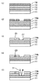
図1は本発明の実施例に係る反射型マスクの製造工程を示す図である。図1(1)に本実施例の反射型マスクブランクス10を示す。基板11は、石英ガラス基板(外形6インチ角、厚さが0.25インチ)である。そして、ガラス基板は機械研磨により、0.2nmRms以下の平滑な表面と100nm以下の平坦度に形成した。
基板11上に形成される多層反射膜12は、13〜14nmの露光光波長帯域に適した多層反射膜を形成するために、本実施例では、Mo/Si周期多層反射膜を採用した。多層反射膜12は、MoとSiをイオンビーム成膜装置(IBD)により基板上に交互に積層して形成した。Si膜4.2nmとMo膜2.8nmを一周期として、40周期積層した後、最後にSi膜を7nm成膜した。合計膜厚は287nmである。この多層反射膜に対し、13.4nmの光の入射角2度での反射率は62.4%であった。又、波長257nmの光に対する反射率は、60%であった。
多層反射膜12上に形成されたバッファ層13は、窒化クロムから構成されており、膜厚は50nmである。この窒化クロムは、Cr:N=90:10(at%)である。このバッファ層13はCrターゲットを用いて、スパッタガスとしてArに窒素を10%添加したガスを用い、DCマグネトロン反応性スパッタ法により形成した。形成されたバッファ層13の結晶状態は微結晶であることをX線回折法にて確認した。バッファ層13表面の257nmの光に対する反射率は、42.1%であった。
Hereinafter, the present invention will be described more specifically with reference to examples.
FIG. 1 is a diagram showing a manufacturing process of a reflective mask according to an embodiment of the present invention. FIG. 1 (1) shows a reflective mask blank 10 of this embodiment. The
In this embodiment, the multilayer
The
バッファ層13上に形成される本実施例の吸収体層下層14は、タンタルホウ素合金の窒化物(TaBN)を膜厚50nmに形成した。この吸収体層下層の材料は、組成は、Ta:B:Nは65.6:16.4:18(at%)とした。この吸収体層下層14は、DCマグネトロン反応性スパッタ法により、TaとBを含む焼結体ターゲットを用い、Arに窒素を添加したガスを用いて成膜した。成膜された吸収体層下層14は、結晶状態はアモルファスであった。又、波長13.4nmのEUV光に対する吸収係数は0.03、波長257nmの光に対する反射率は34.2%であった。
吸収体層下層14上には、吸収体層の最上層15を22nmの厚さに形成した。この最上層は、吸収体層下層14及び、バッファ層13とのエッチング条件及びエッチング選択比、ならびに、波長257nmの検査光に対する低反射率を得る点から、モリブデンシリコン合金の酸窒化物(MoSiON)を選択した。又、その組成比は、Mo:Si:O:N=19:19:43:19(at%)とした。この最上層15は、MoSiターゲットを用い、Arに酸素及び窒素を添加したガスを用いてDCマグネトロン反応性スパッタリング法により成膜した。得られた膜の波長13.4nmのEUV光に対する吸収係数は0.4であった。又、波長257nmの検査光に対する最上層表面の反射率は4.4%、波長13.4nmの光に対する反射率は、0.6%であった。
In the absorber layer
On the absorber layer
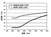
図2は、波長190nm〜800nmの範囲の光に対する、吸収体層最上層表面での反射率及び最上層を形成する前の下層表面での反射率を示すグラフである。同図に示すように、最上層にMoSiON材料を用いることにより、検査波長における反射率を大幅に低下させることができた。
以上のようにして、図1(1)に示す本実施例の反射型マスクブランクス10を得た。
次に、上述した反射型マスクブランクス10から、図1(5)に示す反射型マスク20を製作する方法を説明する。
まず、上記反射型マスクブランクス10の吸収体層最上層15の上に有機系のフォトレジストを膜厚200nm塗布し、EB描画機を用いて描画、現像し、レジストパターンを形成した(図示せず)。
このレジストパターンをマスクとして、SF6ガスを用いて吸収体層の最上層15をドライエッチングし、吸収体層の最上層15にマスクパターン15aを形成した。SF6ガスによる吸収体層の最上層のドライエッチング条件に対する、吸収体層の最上層と吸収体層の下層とのエッチング選択比は、約10であり、下層は最上層のエッチング条件に対し、十分なエッチング耐性を有していた。
更に、最上層上に残存するレジストパターンを硫酸水溶液にて処理し、溶解除去した(図1(2))。
FIG. 2 is a graph showing the reflectance on the surface of the absorber layer uppermost layer and the reflectance on the surface of the lower layer before forming the uppermost layer with respect to light having a wavelength in the range of 190 nm to 800 nm. As shown in the figure, the reflectance at the inspection wavelength could be greatly reduced by using the MoSiON material for the uppermost layer.
As described above, a reflective mask blank 10 of this example shown in FIG. 1 (1) was obtained.
Next, a method of manufacturing the
First, an organic photoresist having a film thickness of 200 nm was applied on the absorber layer
Using this resist pattern as a mask, the
Further, the resist pattern remaining on the uppermost layer was treated with an aqueous sulfuric acid solution and dissolved and removed (FIG. 1 (2)).
次に、最上層に形成されたマスクパターン15aをマスクとして、吸収体層の下層14に吸収体パターン14aを形成した(図1(3))。このパターンの形成は、塩素ガスを用いたエッチングにより行った。吸収体層の下層のエッチング条件において、下層と最上層とのエッチング選択比は約25であり、最上層はわずかに膜厚が減少したが、下層のエッチング条件に十分な耐性を有していた。
まずこの状態で、吸収体パターンの検査を行った。この吸収体パターンの検査は、波長257nmの検査光を用いて、これをマスクの表面に入射させ、最上層の吸収体パターン15aで反射される検査光と、吸収体層が除去されて露出したバッファ層13表面で反射される検査光とのコントラストを観察することにより行った。
本実施例における吸収体パターン15a表面と、バッファ層13表面との検査光に対する反射率の比は1:9.6であり、コントラスト値は81%であり、パターン検査において十分なコントラストが得られた。
この検査結果に基づいて、図1(3)に示すような吸収体層の下層に発生したピンホール欠陥21(白欠陥)及びエッチング不足欠陥22(黒欠陥)を修復した。白欠陥は、集束イオンビーム(FIB)アシストデポジション法により炭素膜23を堆積して修復し、黒欠陥は、レーザービーム照射により残留部分を除去することにより、修復した吸収体層のパターン15b、14bとした(図1(4))。
Next, the
First, in this state, the absorber pattern was inspected. In this inspection of the absorber pattern, the inspection light having a wavelength of 257 nm is used to enter the mask surface, and the inspection light reflected by the
In this embodiment, the ratio of the reflectance to the inspection light between the surface of the
Based on the inspection result, the pinhole defect 21 (white defect) and the under-etching defect 22 (black defect) generated in the lower layer of the absorber layer as shown in FIG. The white defect is repaired by depositing the
次に、マスクの反射領域(吸収体層のパターン15b、14bのない部分)上に残存しているバッファ層13である窒化クロム層を上記吸収体層のパターンに従って除去し、バッファ層のパターン13aを形成した(図1(5))。バッファ層13の除去には、塩素と酸素の混合ガスによるドライエッチングを用いた。バッファ層13のエッチング条件に対するバッファ層と最上層のエッチング選択比は約25であり、最上層はわずかに膜厚が減少したが、バッファ層13のエッチング条件に対し十分な耐性を有していた。最上層の最終膜厚は20nmであった。
以上のようにして、図1(5)に示す構造の反射型マスク20を得た。
ここで、反射型マスク20の最終検査を行った。検査光には、前述の検査と同様、波長257nmの光を用い、これをマスク表面に入射させ、最上層の吸収体パターン15bで反射される検査光と、多層反射膜12上で反射される検査光とのコントラストを観察することにより行った。吸収体パターン15b表面と、バッファ層13が除去されて露出した多層反射膜12表面との検査光に対する反射率の比は1:13.6であり、コントラスト値は86%であり、最終検査においても十分なコントラストが得られた。
以上のようにして、反射型マスク20には、デザインルールが0.07μmの16Gbit-DRAM用のパターンを設計通り形成できている事が検査により確認できた。
Next, the chromium nitride layer, which is the
As described above, a
Here, the final inspection of the
As described above, it was confirmed by inspection that a 16 Gbit-DRAM pattern having a design rule of 0.07 μm was formed on the
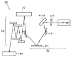
次に図3を参照して、本実施例の反射型マスク20を用いてレジスト付き半導体基板にEUV光によってパターンを転写する方法を説明する。図3は反射型マスクを使用するパターン転写装置の概略構成図である。同図に示すように、パターン転写装置50は、レーザープラズマX線源32、反射型マスク20、縮小光学系33等から概略構成される。縮小光学系33は、X線反射ミラーを用いており、この縮小光学系33により、反射型マスク20で反射されたパターンは通常1/4程度に縮小される。尚、露光波長として13〜14nmの波長帯を使用するので、光路が真空中になるように予め設定した。
このような状態で、レーザープラズマX線源32から得られたEUV光を反射型マスク20に入射し、ここで反射された光を縮小光学系33を通してSiウエハ34上に転写した。反射型マスク20に入射した光は、吸収体のパターンのある部分では、吸収体層に吸収されて反射されず、一方、吸収体パターンのない部分に入射した光は多層反射膜により反射される。このようにして、反射型マスク20から反射される光により形成される像が縮小光学系33に入射する。縮小光学系33を経由した露光光は、Siウエハ34上のレジスト層に転写パターンを露光する。そして、露光済レジストを現像することによってレジストパターンを形成した。
以上のようにして半導体基板上へのパターン転写を行った結果、本実施例の反射型マスクの精度は70nmデザインルールの要求精度である16nm以下であることが確認できた。
Next, with reference to FIG. 3, a method of transferring a pattern by EUV light to a resist-coated semiconductor substrate using the
In this state, EUV light obtained from the laser
As a result of pattern transfer onto the semiconductor substrate as described above, it was confirmed that the accuracy of the reflective mask of this example was 16 nm or less, which is the required accuracy of the 70 nm design rule.
また、比較例として、吸収体層は1層構造とし、上記実施例の吸収体層の下層と同じタンタルホウ素合金の窒化物を用い、膜厚は上記実施例の吸収体層の最上層と下層の合計膜厚とほぼ等しい70nmとし、その他の構成は上記実施例と同様にして反射型マスクブランクスを得た。本比較例は、このように吸収体層を1層構造とし、さらに吸収体層のエッチングの際に有機レジストをマスクとした点が上記実施例と異なる。
本比較例のマスクブランクスの吸収体層上に、有機物質からなる電子線照射用レジストを400nmの厚さに塗布し、このレジストをベーク後、電子線照射して現像し、レジストパターンを形成した。このレジストパターンをマスクとして、吸収体層にパターンを形成した。吸収体層のパターン形成には塩素ガスを用いた。有機物質からなる電子線照射用レジストと吸収体層のエッチング選択比は約1であり、吸収体層のパターン形成後には、有機レジストはオーバーエッチングを行ったこともあり約100nm程度削られていた。吸収体層のパターン形成後、レジストを熱濃硫酸を用いて除去した。
このようにして、吸収体層にパターンを形成した後、上記実施例と同様に、257nmの波長の検査光を用いて吸収体パターンの検査を行った。検査光に対する吸収体層表面での反射率は34.2%であった。吸収体層表面とバッファ層表面での検査光の反射率の比は、1:1.2であり、コントラスト値は10%と小さく、正確な検査が行えなかった。又、形成された吸収体パターンをSEM(走査型電子顕微鏡)で観察したところ、特に線幅の狭い部分において、多数のエッチング不足欠陥(黒欠陥)が観察された。また、設計どおりの形状が得られていない箇所が観察された。
As a comparative example, the absorber layer has a single layer structure, and the same tantalum boron alloy nitride as the lower layer of the absorber layer in the above example is used, and the film thickness is the uppermost layer and the lower layer of the absorber layer in the above example. Reflective mask blanks were obtained in the same manner as in the above example except that the thickness was 70 nm, which was substantially equal to the total film thickness. This comparative example is different from the above-described example in that the absorber layer has a single-layer structure as described above, and an organic resist is used as a mask when the absorber layer is etched.
On the absorber layer of the mask blank of this comparative example, a resist for electron beam irradiation made of an organic material was applied to a thickness of 400 nm, this resist was baked, and developed by electron beam irradiation to form a resist pattern. . Using this resist pattern as a mask, a pattern was formed on the absorber layer. Chlorine gas was used for pattern formation of the absorber layer. The etching selectivity between the electron beam irradiation resist made of an organic material and the absorber layer is about 1, and after the pattern formation of the absorber layer, the organic resist was cut by about 100 nm because of over-etching. . After the pattern formation of the absorber layer, the resist was removed using hot concentrated sulfuric acid.
Thus, after forming a pattern in an absorber layer, similarly to the said Example, the test | inspection of the absorber pattern was performed using the test light of a wavelength of 257 nm. The reflectance on the surface of the absorber layer with respect to the inspection light was 34.2%. The ratio of the reflectance of the inspection light between the absorber layer surface and the buffer layer surface was 1: 1.2, the contrast value was as small as 10%, and an accurate inspection could not be performed. Further, when the formed absorber pattern was observed with an SEM (scanning electron microscope), a large number of etching deficient defects (black defects) were observed particularly in a portion having a narrow line width. Moreover, the location where the shape as designed was not obtained was observed.
(発明の効果)
以上詳細に説明したように、請求項1の発明によれば、基板と、該基板上に順次形成された、露光光を反射する多層反射膜及び露光光を吸収する吸収体層を備えた反射型マスクブランクスであって、吸収体層は、少なくとも最上層と、それ以外の下層とからなる積層構造とし、最上層は、吸収体層に形成された吸収体層のパターンの検査に使用する検査波長の光に対する反射率が20%以下であり、かつ下層へのパターン形成の際のエッチング条件に対し耐性を有する無機材料で形成されているため、その最上層がマスクパターン検査時の低反射層であるとともに、それより下層の吸収体層にパターン形成をする際のエッチングマスク層としての機能を兼ね備えることができる。従って、吸収体層に微細なパターンを形状精度よく形成でき、パターン検査において十分なコントラストが得られ、高精度のパターン転写が可能となる。
また、請求項2の発明によれば、前記最上層は、マスクパターン検査に使用する検査波長の光において、吸収体層の直下の層に対するコントラスト値が40%以上であり、かつ下層へのパターン形成の際のエッチング条件に対し耐性を有する無機材料で形成されているため、マスクパターンの検査時に十分なコントラストが得られると共に、線幅の細いパターンであっても形状精度よく形成でき、高品質な転写像を得ることができる。
また、請求項3の発明によれば、上記反射型マスクブランクスは、吸収体層のパターンの検査に190nm〜260nmの範囲に含まれる検査光を使用する場合に好適である。
(The invention's effect)
As described above in detail, according to the first aspect of the present invention, the substrate, the multilayer reflection film that reflects the exposure light and the absorber layer that absorbs the exposure light, which are sequentially formed on the substrate, are provided. Type mask blanks, in which the absorber layer has a laminated structure composed of at least an uppermost layer and other lower layers, and the uppermost layer is an inspection used to inspect the pattern of the absorber layer formed on the absorber layer Since the reflectance with respect to light of a wavelength is 20% or less and is formed of an inorganic material having resistance to etching conditions when forming a pattern in the lower layer, the uppermost layer is a low reflection layer at the time of mask pattern inspection In addition, it can also have a function as an etching mask layer when pattern formation is performed on the absorber layer below it. Therefore, a fine pattern can be formed on the absorber layer with high shape accuracy, sufficient contrast can be obtained in pattern inspection, and highly accurate pattern transfer can be performed.
Further, according to the invention of
According to a third aspect of the invention, the reflective mask blank is suitable when inspection light included in a range of 190 nm to 260 nm is used for inspection of the pattern of the absorber layer.
また、請求項4の発明によれば、吸収体層の下層にパターンを形成する際の最上層と下層とのエッチング選択比が5以上であることにより、下層の吸収体層にパターン形成をする際のエッチングマスク層としての最上層を薄くできるので、吸収体層に微細なパターンを形状精度よく形成できる。
また、請求項5の発明によれば、吸収体層の下層がタンタル(Ta)を含む材料で、最上層がケイ素(Si)を含む材料でそれぞれ構成されることにより、最上層がパターン検査光に対して低反射層であると同時に、下層とのエッチング選択比を大きくとることができる。
また、請求項6の発明によれば、多層反射膜と吸収体層との間に、更に、吸収体層の下層のパターン形成及びパターン修正の際のエッチング条件に対し耐性を有するバッファ層を設けることにより、吸収体層をパターン形成及びパターン修正する際に、多層反射膜を保護できる。
また、請求項7の発明によれば、バッファ層がクロム(Cr)を含む材料で構成されることにより、とくにTaを含む吸収体層とのエッチング選択比が大きく取れ、多層反射膜表面、バッファ層表面、吸収体層表面の検査波長における反射率の大小関係が好ましく、さらにバッファ層除去時に多層反射膜へのダメージをほとんど与えずに除去できる。
According to the invention of
According to the invention of
According to the invention of claim 6, a buffer layer having resistance to etching conditions for pattern formation and pattern correction of the lower layer of the absorber layer is further provided between the multilayer reflective film and the absorber layer. Thus, the multilayer reflective film can be protected when the absorber layer is patterned and modified.
According to the invention of claim 7, since the buffer layer is made of a material containing chromium (Cr), the etching selectivity with the absorber layer containing Ta can be particularly increased, and the surface of the multilayer reflective film, the buffer can be obtained. The magnitude relationship between the reflectances at the inspection wavelengths on the surface of the layer and the absorber layer is preferable. Further, when removing the buffer layer, it can be removed with little damage to the multilayer reflective film.
また、請求項8の発明によれば、上記反射型マスクブランクスの吸収体層にパターンを形成してなる反射型マスクは、パターン検査において十分なコントラストが得られ、正確な検査が行えるとともに、微細なマスクパターンが形成されるので高精度のパターン転写が可能である。
また、請求項9の発明によれば、最上層にパターンを形成し、次いで該最上層に形成されたパターンをエッチングマスクとして吸収体層の下層のエッチングを行い、下層にパターンを形成するので、吸収体層に微細なパターンを形状精度よく形成できる。
また、請求項10の発明によれば、多層反射膜と吸収体層との間にバッファ層を有する場合、吸収体層の最上層及び下層にパターンを形成した後、該吸収体層に形成されたパターンをマスクとしてバッファ層のエッチングを行い、バッファ層にパターンを形成するので、吸収体層のパターンに従ってバッファ層を除去できる。
According to the invention of
Further, according to the invention of claim 9, a pattern is formed on the uppermost layer, and then the lower layer of the absorber layer is etched using the pattern formed on the uppermost layer as an etching mask to form a pattern on the lower layer. A fine pattern can be formed on the absorber layer with good shape accuracy.
According to the invention of
10 反射型マスクブランクス
11 基板
12 多層反射膜
13 バッファ層
14 吸収体層下層
15 吸収体層最上層
20 反射型マスク
31 EUV光
50 パターン転写装置
DESCRIPTION OF
Claims (9)
前記吸収体層は、少なくとも最上層と、それ以外の下層とからなる積層構造となっており、前記最上層は、前記吸収体層に形成された吸収体層のパターンの検査に使用する検査波長の光に対する反射率が20%以下であり、かつ下層へのパターン形成の際のエッチング条件に対し耐性を有する無機材料で形成されており、
前記吸収体層の下層がタンタル(Ta)を含む材料で、前記最上層がケイ素(Si)を含む材料でそれぞれ構成され、
前記下層にパターンを形成する際における前記最上層と下層とのエッチング選択比が5以上であることを特徴とする反射型マスクブランクス。 A reflective mask blank including a substrate, a multilayer reflective film that reflects exposure light, and an absorber layer that absorbs exposure light, which are sequentially formed on the substrate,
The absorber layer has a laminated structure composed of at least an uppermost layer and other lower layers, and the uppermost layer is an inspection wavelength used for inspecting the pattern of the absorber layer formed on the absorber layer. The light reflectivity is 20% or less, and is formed of an inorganic material having resistance to etching conditions when forming a pattern in the lower layer,
The lower layer of the absorber layer is made of a material containing tantalum (Ta), and the uppermost layer is made of a material containing silicon (Si).
A reflective mask blank, wherein an etching selection ratio between the uppermost layer and the lower layer in forming a pattern in the lower layer is 5 or more.
前記吸収体層は、少なくとも最上層と、それ以外の下層とからなる積層構造となっており、
前記最上層は、前記吸収体層に形成された吸収体層のパターンの検査に使用する検査波長の光において、前記吸収体層下の前記多層反射膜に対する下記の式で示されるコントラスト値が40%以上であり、かつ下層へのパターン形成の際のエッチング条件に対し耐性を有する無機材料で形成されており、
前記吸収体層の下層がタンタル(Ta)を含む材料で、前記最上層がケイ素(Si)を含む材料でそれぞれ構成され、
前記下層にパターンを形成する際における前記最上層と下層とのエッチング選択比が5以上であることを特徴とする反射型マスクブランクス。
(式)コントラスト値(%)=(R2−R1)/(R2+R1)×100
(ただし、R1は検査波長の光に対する最上層表面の反射率、R2は吸収体層下の多層反射膜表面の反射率) A reflective mask blank including a substrate, a multilayer reflective film that reflects exposure light, and an absorber layer that absorbs exposure light, which are sequentially formed on the substrate,
The absorber layer has a laminated structure composed of at least an uppermost layer and other lower layers,
The uppermost layer has a contrast value represented by the following equation with respect to the multilayer reflective film under the absorber layer in light having an inspection wavelength used for inspection of the pattern of the absorber layer formed on the absorber layer. % And is formed of an inorganic material having resistance to etching conditions when forming a pattern in the lower layer,
The lower layer of the absorber layer is made of a material containing tantalum (Ta), and the uppermost layer is made of a material containing silicon (Si).
A reflective mask blank, wherein an etching selection ratio between the uppermost layer and the lower layer in forming a pattern in the lower layer is 5 or more.
(Formula) Contrast value (%) = (R 2 −R 1 ) / (R 2 + R 1 ) × 100
(Where R 1 is the reflectance of the surface of the uppermost layer with respect to the light of the inspection wavelength, and R 2 is the reflectance of the surface of the multilayer reflective film below the absorber layer)
(式)コントラスト値(%)=(R2−R1)/(R2+R1)×100
(ただし、R1は検査波長の光に対する最上層表面の反射率、R2は吸収体層下の多層反射膜表面の反射率) The uppermost layer has a contrast value represented by the following equation with respect to the multilayer reflective film under the absorber layer in light having an inspection wavelength used for inspection of the pattern of the absorber layer formed on the absorber layer. The reflective mask blank according to claim 1, which is at least%.
(Formula) Contrast value (%) = (R 2 −R 1 ) / (R 2 + R 1 ) × 100
(Where R 1 is the reflectance of the surface of the uppermost layer with respect to the light of the inspection wavelength, and R 2 is the reflectance of the surface of the multilayer reflective film below the absorber layer)
Priority Applications (1)
| Application Number | Priority Date | Filing Date | Title |
|---|---|---|---|
| JP2007241562A JP4792147B2 (en) | 2007-09-18 | 2007-09-18 | Reflective mask blanks and reflective masks |
Applications Claiming Priority (1)
| Application Number | Priority Date | Filing Date | Title |
|---|---|---|---|
| JP2007241562A JP4792147B2 (en) | 2007-09-18 | 2007-09-18 | Reflective mask blanks and reflective masks |
Related Parent Applications (1)
| Application Number | Title | Priority Date | Filing Date |
|---|---|---|---|
| JP2002195458A Division JP4212025B2 (en) | 2002-07-04 | 2002-07-04 | REFLECTIVE MASK BLANK, REFLECTIVE MASK, AND METHOD FOR PRODUCING REFLECTIVE MASK |
Publications (3)
| Publication Number | Publication Date |
|---|---|
| JP2007335908A JP2007335908A (en) | 2007-12-27 |
| JP2007335908A5 JP2007335908A5 (en) | 2010-03-25 |
| JP4792147B2 true JP4792147B2 (en) | 2011-10-12 |
Family
ID=38935010
Family Applications (1)
| Application Number | Title | Priority Date | Filing Date |
|---|---|---|---|
| JP2007241562A Expired - Lifetime JP4792147B2 (en) | 2007-09-18 | 2007-09-18 | Reflective mask blanks and reflective masks |
Country Status (1)
| Country | Link |
|---|---|
| JP (1) | JP4792147B2 (en) |
Families Citing this family (10)
| Publication number | Priority date | Publication date | Assignee | Title |
|---|---|---|---|---|
| JP2009210802A (en) * | 2008-03-04 | 2009-09-17 | Asahi Glass Co Ltd | Reflective mask blank for extreme ultraviolet lithography |
| EP2256789B1 (en) * | 2008-03-18 | 2012-07-04 | Asahi Glass Company, Limited | Reflective mask blank for euv lithography |
| JP2009252788A (en) * | 2008-04-01 | 2009-10-29 | Asahi Glass Co Ltd | Reflective mask blank for euv lithography |
| CN102067283A (en) | 2008-06-19 | 2011-05-18 | 旭硝子株式会社 | Reflective mask blank for EUV lithography |
| WO2010007955A1 (en) * | 2008-07-14 | 2010-01-21 | 旭硝子株式会社 | Reflective mask blank for euv lithography and reflective mask for euv lithography |
| WO2010074125A1 (en) * | 2008-12-26 | 2010-07-01 | Hoya株式会社 | Reflective mask blank and reflective mask manufacturing method |
| JP5549264B2 (en) * | 2010-02-17 | 2014-07-16 | 大日本印刷株式会社 | REFLECTIVE MASK BLANK AND REFLECTIVE MASK, ITS MANUFACTURING METHOD, AND INSPECTION METHOD |
| WO2011108470A1 (en) | 2010-03-02 | 2011-09-09 | 旭硝子株式会社 | Reflection-type mask blank for euv lithography and method for producing the same |
| JP5594106B2 (en) * | 2010-12-09 | 2014-09-24 | 大日本印刷株式会社 | Reflective mask and method of manufacturing the same |
| JP5881633B2 (en) * | 2013-02-28 | 2016-03-09 | 株式会社東芝 | Light-reflective photomask for EUV exposure, mask blank, and method for manufacturing semiconductor device |
Family Cites Families (10)
| Publication number | Priority date | Publication date | Assignee | Title |
|---|---|---|---|---|
| JP2000058830A (en) * | 1998-05-28 | 2000-02-25 | Texas Instr Inc <Ti> | Antireflection structure and manufacture thereof |
| US6316167B1 (en) * | 2000-01-10 | 2001-11-13 | International Business Machines Corporation | Tunabale vapor deposited materials as antireflective coatings, hardmasks and as combined antireflective coating/hardmasks and methods of fabrication thereof and application thereof |
| US6890448B2 (en) * | 1999-06-11 | 2005-05-10 | Shipley Company, L.L.C. | Antireflective hard mask compositions |
| JP2001110709A (en) * | 1999-10-08 | 2001-04-20 | Nikon Corp | Multilayer film reflecting mirror, aligner and manufacturing method of integrated circuit |
| JP2001176788A (en) * | 1999-12-21 | 2001-06-29 | Hitachi Ltd | Pattern-forming method and semiconductor device |
| JP4397496B2 (en) * | 2000-02-25 | 2010-01-13 | Okiセミコンダクタ株式会社 | Reflective exposure mask and EUV exposure apparatus |
| JP2001326173A (en) * | 2000-05-16 | 2001-11-22 | Hitachi Ltd | Pattern-forming method |
| JP3441711B2 (en) * | 2000-11-02 | 2003-09-02 | Hoya株式会社 | Halftone type phase shift mask and halftone type phase shift mask blank |
| JP2002246299A (en) * | 2001-02-20 | 2002-08-30 | Oki Electric Ind Co Ltd | Reflecting type exposure mask, its manufacturing method and semiconductor element |
| JP2003133205A (en) * | 2001-10-24 | 2003-05-09 | Oki Electric Ind Co Ltd | Reflex mask, method of manufacturing the same, and method of cleaning the same |
-
2007
- 2007-09-18 JP JP2007241562A patent/JP4792147B2/en not_active Expired - Lifetime
Also Published As
| Publication number | Publication date |
|---|---|
| JP2007335908A (en) | 2007-12-27 |
Similar Documents
| Publication | Publication Date | Title |
|---|---|---|
| JP4212025B2 (en) | REFLECTIVE MASK BLANK, REFLECTIVE MASK, AND METHOD FOR PRODUCING REFLECTIVE MASK | |
| JP4792147B2 (en) | Reflective mask blanks and reflective masks | |
| KR101707591B1 (en) | Reflective mask blank and reflective mask manufacturing method | |
| US8709685B2 (en) | Reflective mask blank and method of manufacturing a reflective mask | |
| JP4163038B2 (en) | Reflective mask blank, reflective mask, and semiconductor manufacturing method | |
| JP4535270B2 (en) | Method for manufacturing a reflective mask | |
| JP4926521B2 (en) | REFLECTIVE MASK BLANK, REFLECTIVE MASK, AND METHOD FOR MANUFACTURING SEMICONDUCTOR DEVICE | |
| WO2003085709A9 (en) | Reflection type mask blank and reflection type mask and production methods for them | |
| US20110281207A1 (en) | Reflective mask blank and method of manufacturing a reflective mask | |
| US8021807B2 (en) | Reflective mask blank and method of producing the same, and method of producing a reflective mask | |
| JP5009590B2 (en) | Mask blank manufacturing method and mask manufacturing method | |
| TWI518445B (en) | A reflective mask substrate and a method of manufacturing the same, and a reflection type mask | |
| US20100084375A1 (en) | Method of producing a reflective mask | |
| JP5018212B2 (en) | Reflective photomask blank, reflective photomask, and semiconductor device manufacturing method | |
| JP2008078551A (en) | Reflective phototmask blank, reflective phototmask, and method of manufacturing semiconductor device | |
| JP2021105727A (en) | Manufacturing method of reflection type mask, reflection type mask blank and semiconductor device | |
| JP2004281967A (en) | Reflective mask blank and reflective mask | |
| JP2005037798A (en) | Reflective mask blank, its manufacturing method, reflective mask, substrate with reflective multilayer film, and its manufacturing method | |
| JP4541654B2 (en) | Method for manufacturing a reflective mask |
Legal Events
| Date | Code | Title | Description |
|---|---|---|---|
| A521 | Request for written amendment filed |
Free format text: JAPANESE INTERMEDIATE CODE: A523 Effective date: 20100205 |
|
| A131 | Notification of reasons for refusal |
Free format text: JAPANESE INTERMEDIATE CODE: A131 Effective date: 20100615 |
|
| A521 | Request for written amendment filed |
Free format text: JAPANESE INTERMEDIATE CODE: A523 Effective date: 20100816 |
|
| TRDD | Decision of grant or rejection written | ||
| A01 | Written decision to grant a patent or to grant a registration (utility model) |
Free format text: JAPANESE INTERMEDIATE CODE: A01 Effective date: 20110705 |
|
| A01 | Written decision to grant a patent or to grant a registration (utility model) |
Free format text: JAPANESE INTERMEDIATE CODE: A01 |
|
| A61 | First payment of annual fees (during grant procedure) |
Free format text: JAPANESE INTERMEDIATE CODE: A61 Effective date: 20110724 |
|
| FPAY | Renewal fee payment (event date is renewal date of database) |
Free format text: PAYMENT UNTIL: 20140729 Year of fee payment: 3 |
|
| R150 | Certificate of patent or registration of utility model |
Ref document number: 4792147 Country of ref document: JP Free format text: JAPANESE INTERMEDIATE CODE: R150 Free format text: JAPANESE INTERMEDIATE CODE: R150 |
|
| R250 | Receipt of annual fees |
Free format text: JAPANESE INTERMEDIATE CODE: R250 |
|
| R250 | Receipt of annual fees |
Free format text: JAPANESE INTERMEDIATE CODE: R250 |
|
| R250 | Receipt of annual fees |
Free format text: JAPANESE INTERMEDIATE CODE: R250 |
|
| R250 | Receipt of annual fees |
Free format text: JAPANESE INTERMEDIATE CODE: R250 |
|
| R250 | Receipt of annual fees |
Free format text: JAPANESE INTERMEDIATE CODE: R250 |
|
| R250 | Receipt of annual fees |
Free format text: JAPANESE INTERMEDIATE CODE: R250 |
|
| R250 | Receipt of annual fees |
Free format text: JAPANESE INTERMEDIATE CODE: R250 |
|
| R250 | Receipt of annual fees |
Free format text: JAPANESE INTERMEDIATE CODE: R250 |
|
| EXPY | Cancellation because of completion of term |