JP4792113B2 - Interprocessor interrupt - Google Patents
Interprocessor interrupt Download PDFInfo
- Publication number
- JP4792113B2 JP4792113B2 JP2010002051A JP2010002051A JP4792113B2 JP 4792113 B2 JP4792113 B2 JP 4792113B2 JP 2010002051 A JP2010002051 A JP 2010002051A JP 2010002051 A JP2010002051 A JP 2010002051A JP 4792113 B2 JP4792113 B2 JP 4792113B2
- Authority
- JP
- Japan
- Prior art keywords
- memory location
- processor
- interrupt
- inter
- instruction
- Prior art date
- Legal status (The legal status is an assumption and is not a legal conclusion. Google has not performed a legal analysis and makes no representation as to the accuracy of the status listed.)
- Expired - Fee Related
Links
Images
Classifications
-
- G—PHYSICS
- G06—COMPUTING; CALCULATING OR COUNTING
- G06F—ELECTRIC DIGITAL DATA PROCESSING
- G06F9/00—Arrangements for program control, e.g. control units
- G06F9/06—Arrangements for program control, e.g. control units using stored programs, i.e. using an internal store of processing equipment to receive or retain programs
- G06F9/46—Multiprogramming arrangements
- G06F9/48—Program initiating; Program switching, e.g. by interrupt
- G06F9/4806—Task transfer initiation or dispatching
- G06F9/4812—Task transfer initiation or dispatching by interrupt, e.g. masked
-
- G—PHYSICS
- G06—COMPUTING; CALCULATING OR COUNTING
- G06F—ELECTRIC DIGITAL DATA PROCESSING
- G06F9/00—Arrangements for program control, e.g. control units
- G06F9/06—Arrangements for program control, e.g. control units using stored programs, i.e. using an internal store of processing equipment to receive or retain programs
- G06F9/46—Multiprogramming arrangements
- G06F9/54—Interprogram communication
- G06F9/544—Buffers; Shared memory; Pipes
Landscapes
- Engineering & Computer Science (AREA)
- Theoretical Computer Science (AREA)
- Software Systems (AREA)
- Physics & Mathematics (AREA)
- General Engineering & Computer Science (AREA)
- General Physics & Mathematics (AREA)
- Computer Hardware Design (AREA)
- Multi Processors (AREA)
- Memory System Of A Hierarchy Structure (AREA)
- Debugging And Monitoring (AREA)
- Bus Control (AREA)
Description
本発明の一実施形態はコンピュータ動作全般に関し、特にプロセッサ間割り込みに関する。 One embodiment of the invention relates generally to computer operations, and more particularly to interprocessor interrupts.
コンピュータは、物理的なプロセッサ及び論理的なプロセッサを含み得る複数のプロセッサを備え得る。オペレーティングシステムはプロセッサ間割り込み(IPI)を利用して、システム内のプロセッサ間で要求を受け渡すことができる。オペレーティングシステムはプロセッサ間割り込みを使用して、1つのプロセッサに1つ又は複数の他のプロセッサに対する特定のアクションを開始させることができる。このようなアクションは、プロセッサが割り込みを他のプロセッサに送ってTLBエントリの無効化を要求するTLB(変換ルックアサイドバッファ)シュートダウン割り込みを含み得る。受け取り側のプロセッサは、線形アドレスマッピングの変更又は特定のメモリ範囲のメモリキャッシュ属性の変更等、送り側のプロセッサが行ったグローバルな変更に応答してキャッシュフラッシュを開始することができる。 The computer may comprise a plurality of processors that may include physical processors and logical processors. The operating system can use an interprocessor interrupt (IPI) to pass requests between processors in the system. The operating system can use interprocessor interrupts to cause one processor to initiate specific actions for one or more other processors. Such actions may include TLB (Translation Lookaside Buffer) shoot down interrupts where a processor sends an interrupt to another processor to request invalidation of the TLB entry. The receiving processor can initiate a cache flush in response to a global change made by the sending processor, such as a change in linear address mapping or a memory cache attribute for a particular memory range.
しかし、プロセッサ間割り込み信号は、送り側のプロセッサ及び受け取り側のプロセッサの両方に大きなオーバヘッドを必要とし得る。送り側のプロセッサはメモリアクセスを行い、ローカルアドバンストプログラマブル割り込みコントローラ(APIC:local advanced programmable interrupt controller)等のプログラマブル割り込みコントローラを通して割り込みを送る必要がある。同様に、受け取り側プロセッサも割り込みを受け取るプロセスにおいて相当なオーバヘッドを負担する恐れがある。 However, interprocessor interrupt signals may require significant overhead on both the sending processor and the receiving processor. The sending processor needs to access the memory and send an interrupt through a programmable interrupt controller such as a local advanced programmable interrupt controller (APIC). Similarly, the receiving processor may incur significant overhead in the process receiving the interrupt.
本発明は、本発明の実施形態を例示するために使用される以下の説明及び添付図面を参照することによって最良に理解することができる。 The invention may best be understood by referring to the following description and accompanying drawings that are used to illustrate embodiments of the invention.
マルチプロセッサシステム内でのプロセッサ間割り込みのための方法及び装置について説明する。 A method and apparatus for interprocessor interrupts in a multiprocessor system is described.
本発明の一実施形態下では、プロセッサ間割り込み関数は割り込みを呼び出す命令を使用して行われる。本明細書ではこの命令をMcall命令と呼ぶが、この命令は任意の名称を有することができる。実施形態では、送り側プロセッサへの関数の動作コストはライトバックメモリロケーションへの記憶であり、受け取り側へのコストは関数への強制呼び出しである。本発明の一実施形態はプロセッサ間割り込みの動作コストを大幅に削減し、それによってシステムパフォーマンスを向上させることができる。 Under one embodiment of the present invention, the interprocessor interrupt function is performed using an instruction that invokes an interrupt. This instruction is referred to herein as the Mcall instruction, but this instruction can have any name. In an embodiment, the operating cost of the function to the sending processor is storage to the write-back memory location, and the cost to the receiving side is a forced call to the function. One embodiment of the present invention can significantly reduce the operating cost of interprocessor interrupts, thereby improving system performance.
本発明の一実施形態によれば、割り込み関数は、メモリシステムを通して送られる信号によって実行される。送り側プロセッサは、ライトバックメモリロケーションへの記憶を行う。その結果、記憶により受け取り側に関数呼び出しが発生する。この動作は、APICを通して送られる従来の割り込みと対照を成すことができる。この実施形態は、プロセッサ間割り込みを送るコストを削減することによってマルチプロセッサ環境及びマルチスレッド環境でのオペレーティングシステムのパフォーマンスを向上させることができる。本発明の一実施形態下では、APICなしで、又は代替の信号動作を有するシステム内でなく、プロセッサ間割り込み関数を実行することができる。 According to one embodiment of the invention, the interrupt function is performed by a signal sent through the memory system. The sending processor stores to the write-back memory location. As a result, a function call occurs on the receiving side due to storage. This operation can be contrasted with conventional interrupts sent through APIC. This embodiment can improve operating system performance in multiprocessor and multithreaded environments by reducing the cost of sending interprocessor interrupts. Under one embodiment of the present invention, an interprocessor interrupt function can be executed without APIC or in a system with alternative signal behavior.
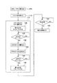
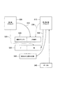
プロセッサ間割り込みを送る従来のメカニズムを図1に示す。この図では、第1の開始側すなわち送り側プロセッサが割り込みを第2の受け取り側すなわちターゲットプロセッサに提供する。図1に提供する例は2つの32ビット書き込み動作で書かれる64ビットコマンドが関係する。このシーケンスでは、第1のプロセッサは以下のタスクを実行する。
1.プロセッサローカルAPICタスク優先度レジスタへの書き込み105を介して割り込み要求レベル(IRQL)を上げる。これは非キャッシュロケーションへの書き込みである。
2.プロセッサローカルAPIC割り込みコマンドレジスタに書き込むコマンドを作成する(メモリロケーション又はレジスタに)110。パラメータの中でも特に、このコマンドはターゲットプロセッサ及びターゲットプロセッサへの割り込みに使用すべき割り込みベクトルVを指定する。割り込みベクトルVは、プロセッサ間割り込みを送ったことに応答してターゲットプロセッサにおいて実行され得る割り込みサービスルーチンに対応し得る。
3.コマンドをプロセッサローカルAPIC割り込みコマンドレジスタ(ICR)に書き込む115。これは非キャッシュロケーションへの書き込みである。コマンドを書き込むプロセスは以下を含み得る。
a.割り込みのディセーブル動作120
b.ローカルAPICの空きを待つ125。これは割り込みコマンドレジスタのBUSYビットをポーリングすることによって行うことができる。
c.コマンドの上位32ビットをAPIC割り込みコマンドレジスタハイワードに書き込む130。
d.コマンドの下位32ビットをAPIC割り込みコマンドレジスタローワードに書き込む135。
e.ローカルAPICの空きを待つ140。
f.割り込み動作を再びイネーブルする145。
4.ターゲットプロセッサが、特定のデータ値を特定のメモリロケーションに書き込むことにより、プロセッサ間割り込みを受け取ったことに対して肯定応答するのを待つ150。この書き込みは、ターゲットプロセッサに送ったまさにその割り込みに対しての処理の一環として行われ得る。
5.通常動作を再開する155。
A conventional mechanism for sending interprocessor interrupts is shown in FIG. In this figure, a first initiator or sender processor provides an interrupt to a second receiver or target processor. The example provided in FIG. 1 involves a 64-bit command written in two 32-bit write operations. In this sequence, the first processor performs the following tasks:
1. The interrupt request level (IRQL) is raised through writing 105 to the processor local APIC task priority register. This is a write to a non-cache location.
2. Create a command to write to the processor local APIC interrupt command register (in a memory location or register) 110. Among other parameters, this command specifies the target processor and the interrupt vector V to be used for interrupting the target processor. The interrupt vector V may correspond to an interrupt service routine that may be executed at the target processor in response to sending an interprocessor interrupt.
3. Write the command to the processor local APIC interrupt command register (ICR) 115. This is a write to a non-cache location. The process of writing a command can include:
a.
b. Wait for a local APIC to be available 125. This can be done by polling the BUSY bit of the interrupt command register.
c. Write the upper 32 bits of the command to the APIC interrupt command register
d. Write the lower 32 bits of the command to the APIC interrupt command register
e. Wait 140 for local APIC availability.
f. The interrupt operation is re-enabled 145.
4). Wait 150 for the target processor to acknowledge receipt of the interprocessor interrupt by writing a specific data value to a specific memory location. This writing can be done as part of the processing for that very interrupt sent to the target processor.
5. Normal operation resumes 155.
受け取り側プロセッサでは、割り込みは従来通り、ローカルAPIC割り込み送出メカニズムに組み込まれたロジックを介してラッチされてプロセッサコアに送出される。示す割り込みメカニズムは、プロセッサコアが動作している割り込み優先度(APICタスク優先度レジスタに反映される)、より高い優先度を有し得る他の保留中の割り込み、及びプロセッサコアの割り込み可能性状態(interruptibility state)を考慮する。プロセッサコアが割り込みをイネーブルさせ、プロセッサ間割り込みに対応するベクトルが保留中の最高優先度割り込みベクトルである場合、ローカルAPICはベクトルをコアにディスパッチする。 In the receiving processor, interrupts are conventionally latched and delivered to the processor core via logic built into the local APIC interrupt delivery mechanism. The interrupt mechanism shown is the interrupt priority at which the processor core is operating (as reflected in the APIC task priority register), other pending interrupts that may have a higher priority, and the interruptability status of the processor core (Interruptility state) is considered. If the processor core enables interrupts and the vector corresponding to the interprocessor interrupt is the pending highest priority interrupt vector, the local APIC dispatches the vector to the core.
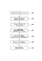
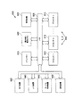
受け取り側プロセッサでの従来のイベントシーケンスを図2に示す。受け取り側プロセッサでのプロセッサ間割り込みプロセスは以下を含み得る。
1.プロセッサのローカルAPICが割り込みベクトルVをディスパッチし205、これはプロセッサコアへの割り込みサービスルーチン(ISR)に対応する。ブート時に、OSは、割り込みサービスルーチンと共に割り込みゲートを含むように、ベクトルVに対応する割り込み記述子テーブルエントリをプログラムしているであろう。
2.タスク優先度レジスタレベルをベクトルVに対応するレベルに上げる210。
3.プロセッサコアが割り込み記述子テーブルを介してベクトルVをディスパッチする215。
4.プロセッサ間割り込みに対応する割り込みサービスルーチンが割り込みをディセーブルして制御権を獲得する220。
5.割り込みサービスルーチンがメモリロケーションに書き込み、送り側プロセッサにプロセッサ間割り込みを受け取ったことを通知する225。
6.プロセッサ間割り込みのアクションを実行する230。
7.通常動作を再開する235。
A conventional event sequence at the receiving processor is shown in FIG. The interprocessor interrupt process at the receiving processor may include:
1. The processor's local APIC dispatches the
2. Increase task priority register level to a level corresponding to
3. The processor core dispatches 215 the vector V via the interrupt descriptor table.
4). An interrupt service routine corresponding to the inter-processor interrupt disables the interrupt and
5. The interrupt service routine writes to the memory location and notifies 225 that the sending processor has received an interprocessor interrupt.
6). An inter-processor interrupt action is executed 230.
7). Normal operation resumes 235.
本発明の一実施形態下では、割り込み動作に命令(この説明ではMcall命令)を使用することで、送り側プロセッサ及び受け取り側プロセッサの動作シーケンスを簡略化することができる。ブート時に、マルチプロセッサシステム内の各プロセッサは、プロセッサ間割り込み関数等、Mcall命令を介して割り込みサービスルーチンを受け取ったときにカーネルモードで実行されていたであろう割り込みサービスルーチンに対応する関数を登録する。しかし、この動作は別法として、モデル固有レジスタの使用を含め、他のメカニズムにより実現することもできる。 Under one embodiment of the present invention, the operation sequence of the sending processor and the receiving processor can be simplified by using instructions (in this description, Mcall instructions) for interrupt operations. At boot time, each processor in the multiprocessor system registers a function corresponding to the interrupt service routine that would have been executed in kernel mode when the interrupt service routine was received via the Mcall instruction, such as an interprocessor interrupt function. To do. However, this operation can alternatively be accomplished by other mechanisms, including the use of model specific registers.
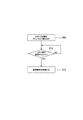
図3は、送り側プロセッサのプロセッサ間割り込みシーケンスの一実施形態の図である。送り側プロセッサのプロセスは以下を含み得る。
1.線形アドレスXへのプロセッサ間割り込み要求のメモリ書き込みを実行する305。
2.受け取り側プロセッサが、特定のメモリロケーションをポーリングして値が変更されたか否かを判断することにより、プロセッサ間割り込みを受け取ったことに対して肯定応答するのを待つ310。その値は、受け取り側プロセッサに対する割り込みサービスの一部として、書き込みにより変更される。この動作はプロセッサ間割り込みの送信の場合には必要なく、いくつかの実施形態では、動作は、メモリロケーションのポーリングなしで、又は割り込みの受信に対する肯定応答を受け取ることなく再開することができる。
3.メモリロケーションが値を変更していた場合、通常動作を再開する315。
FIG. 3 is a diagram of one embodiment of an inter-processor interrupt sequence for the sending processor. The sending processor process may include:
1. The memory write of the interprocessor interrupt request to the linear address X is executed 305.
2. Wait 310 for the receiving processor to acknowledge that it has received an interprocessor interrupt by polling a particular memory location to determine if the value has changed. Its value is changed by writing as part of the interrupt service to the receiving processor. This operation is not necessary in the case of sending interprocessor interrupts, and in some embodiments, the operation can be resumed without polling the memory location or without receiving an acknowledgment for the receipt of the interrupt.
3. If the memory location has changed value, normal operation resumes 315.
図3に示す例は、割り込みが1つの受け取り側プロセッサに送られる例を示す。プロセッサ間割り込みは複数のプロセッサに送ることができる。一実施形態では、複数のプロセッサが単一のメモリロケーションを監視してプロセッサ間割り込みを検出する。別の実施形態では、各プロセッサが別個のメモリロケーションを監視することができる。プロセッサ間割り込みが複数のターゲットプロセッサに送られる場合、送り側プロセッサは、そのプロセッサが監視しているメモリロケーションへの書き込みを実行することができ、又は複数の書き込み、すなわちターゲットプロセッサが監視している各アドレスへの書き込みを実行することができる。本発明の一実施形態下では、実行される各書き込みはキャッシュメモリロケーションに対しての書き込みであるので、従来のシーケンスでのアンキャッシュタスク優先度レジスタアドレスへの書き込みよりもはるかに高速である。 The example shown in FIG. 3 shows an example where an interrupt is sent to one receiving processor. Interprocessor interrupts can be sent to multiple processors. In one embodiment, multiple processors monitor a single memory location to detect interprocessor interrupts. In another embodiment, each processor can monitor a separate memory location. If an interprocessor interrupt is sent to multiple target processors, the sending processor can perform a write to the memory location that the processor is monitoring, or multiple writes, ie the target processor is monitoring Writing to each address can be executed. Under one embodiment of the present invention, each write performed is a write to a cache memory location, which is much faster than a write to an uncached task priority register address in a conventional sequence.
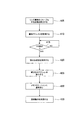
図4は受け取り側プロセッサシーケンスの図である。本発明の一実施形態下では、Mcall動作を使用したプロセッサ間割り込みの受け取り側プロセッサの動作は以下を含み得る。
1.カーネルモードで、プロセッサ間割り込みを受信したときにリング遷移(ring transition)をイネーブルする状態を確立する405。
2.メモリロケーション<Linear Address X>を監視する410。メモリロケーションへの書き込みはプロセッサ間割り込み要求を示す。
3.ユーザモード又はカーネルモードのいずれかでプロセッサ間割り込みを検出すると、現在の状態を保存する420。
4.割り込みMcall<IPI ISR Linear Address>を実行する425。
5.関数の実行には、送り側プロセッサがポーリングしているメモリロケーションへの書き込みが含まれ得る430。
6.通常動作を再開する435。
FIG. 4 is a diagram of the receiving processor sequence. Under one embodiment of the present invention, the operation of the processor receiving the interprocessor interrupt using the Mcall operation may include:
1. In kernel mode, establish 405 a state that enables ring transition when an interprocessor interrupt is received.
2.
3. If an interprocessor interrupt is detected in either user mode or kernel mode, the current state is saved 420.
4). The interrupt Mcall <IPI ISR Linear Address> is executed 425.
5. Execution of the function may include 430 writing to a memory location that the sending processor is polling.
6). Normal operation resumes 435.
この実施形態下では、Mcall命令は受け取り側プロセッサを、プロセッサが書き込みについて線形アドレスXを監視し、書き込み動作が検出されると実行制御権をIPI ISR線形アドレスに移す状態にする。リング遷移は必要に応じて行われ、スタックにおいて適切な状態が確立され、プロセッサ優先度レベルが適切な優先度に上げられる。 Under this embodiment, the Mcall instruction puts the receiving processor into a state where the processor monitors the linear address X for writes and transfers execution control to the IPI ISR linear address when a write operation is detected. Ring transitions are made as needed, an appropriate state is established in the stack, and the processor priority level is raised to the appropriate priority.
図5は、第1の送り側プロセッサと第2の受け取り側プロセッサの間のシーケンスの一実施形態を示す。この例示では、送り側プロセッサ505はプロセッサ間割り込みを受け取り側プロセッサ510に送っている。他の例示では、割り込みを複数のプロセッサに送ることができる。送り側プロセッサ505はプロセッサ間割り込み要求515を図では線形アドレスX520として示すアドレスに書き込む。線形アドレスX520は受け取り側プロセッサ510によって監視される535。次いで、送り側プロセッサ505はY530として例示中に示すメモリロケーションをポーリングする525。メモリロケーションY530での値の変更は、受け取り側プロセッサ510が割り込み要求を受け取ったことの肯定応答を示す。しかし、受け取りに対する肯定応答は必ずしもプロセッサ間割り込み要求の送信に必要なものではなく、いくつかの実施形態では、送り側プロセッサ505は、メモリロケーションをポーリングすることなく、又は肯定応答を受け取ることなく通常動作を開始することができる。
FIG. 5 illustrates one embodiment of a sequence between a first sending processor and a second receiving processor. In this example, the sending
線形アドレスX520を監視535している受け取り側プロセッサ510には、線形アドレスX520への書き込みが発生したときに割り込み要求が通知される。カーネルモードにおいて、受け取り側プロセッサは、プロセッサ間割り込みを受け取ったときに、リング遷移をイネーブルする状態を確立していることになる。割り込みを受け取ると、受け取り側プロセッサの現在の状態が保存される540。線形プロセッサが割り込みを行い、割り込みのための呼び出しはMcall<IPI ISR Linear Address>545として示されている。関数の実行には、送り側プロセッサ505がポーリングしている525メモリロケーションY530への書き込み550を含み得る。メモリロケーションY530での値の変更が検出されると、送り側プロセッサは通常動作を再開することができる。プロセッサ間割り込みを完了すると、受け取り側プロセッサは通常動作を再開することができる。
The receiving
本明細書に記載する技法は多くの異なる環境で使用することができる。図6は、本発明の一実施形態と併せて使用することができる例示的なコンピュータのブロック図である。本発明の一実施形態下では、コンピュータは組込みシステム又は他の専用コンピュータを含むことができる。組込みシステム又は他の専用コンピュータは、本明細書において述べる特定の構成要素及び特徴なしでも動作することができる。 The techniques described herein can be used in many different environments. FIG. 6 is a block diagram of an exemplary computer that can be used in conjunction with one embodiment of the present invention. Under one embodiment of the present invention, the computer may include an embedded system or other dedicated computer. An embedded system or other special purpose computer may operate without the specific components and features described herein.
本発明の一実施形態下では、コンピュータ600は、情報を通信するためのバス605又は他の通信手段、及び第1のバス605に結合された情報を処理するための1つ又は複数のプロセッサ610(611、612として示し、613に続く)等の処理手段を備える。プロセッサ610のいずれも、プロセッサ間割り込みを他の1つ又は複数のプロセッサに提供することができる。各プロセッサは、プロセッサ間割り込み動作のための実行ユニット及びロジックを備えることができる。
Under one embodiment of the present invention, the
コンピュータ600は、情報及びプロセッサ610が実行する命令を記憶するためのメインメモリ615としてランダムアクセスメモリ(RAM)又は他の動的記憶装置をさらに備える。メインメモリ615は、プロセッサ610が命令を実行している間に変数又は他の中間情報を一時的に記憶するためにも使用することができる。コンピュータ600は、プロセッサ610の静的な情報及び命令を記憶するための読み取り専用メモリ(ROM)620及び/又は他の静的記憶装置を備えることもできる。
情報及び命令を記憶するためのデータ記憶装置625もコンピュータ600のバス605に結合することができる。データ記憶装置625は、磁気ディスク又は光ディスク並びにそれに対応するドライブ、フラッシュメモリ若しくは他の不揮発性メモリ、又は他のメモリ装置を含むことができる。このような要素は共に結合してもよく、又は別個の構成要素であってもよく、コンピュータ600の他の要素のパーツを利用する。
A
コンピュータ600は、バス605を介して、情報をエンドユーザに向けて表示するための、液晶ディスプレイ(LCD)又は他の表示技術等の表示装置630にも結合することができる。環境によっては、表示装置は、入力装置の少なくとも一部としても利用されるタッチスクリーンであることができる。環境によっては、表示装置630は、可聴情報を提供するためのスピーカ等の聴覚装置であることができ、又は聴覚装置を備えることができる。入力装置640をバス605に結合して、情報及び/又はコマンド選択をプロセッサ610に通信することができる。各種実施態様では、入力装置640はキーボード、キーパッド、タッチスクリーン及びスタイラス、音声作動システム、他の入力装置、又はこのような装置の組み合わせであることができる。備えることができる別のタイプのユーザ入力装置は、方向情報及びコマンド選択をプロセッサ610に通信するとともに表示装置630上のカーソルの移動を制御するための、マウス、トラックボール、又はカーソル方向キー等のカーソル制御装置645である。
The
通信装置650もバス605に結合することができる。特定の実施態様に応じて、通信装置650は送受信器、ワイヤレスモデム、ネットワークインタフェースカード、又は他のインタフェース装置を備えることができる。コンピュータ600は、通信装置650を使用して、インターネット、ローカルエリアネットワーク、又は別の環境へのリンクを含むことができるネットワーク又は他の装置にリンクすることができる。
A
上記説明中、説明を目的として、本発明の完全な理解を提供するために多くの特定の詳細について述べた。しかし、本発明はこれら特定の詳細のいくつかなしで実施することができることが当業者に理解されよう。他の場合では、既知の構造及び装置についてはブロック図形態で示した。 In the above description, for the purposes of explanation, numerous specific details are set forth in order to provide a thorough understanding of the present invention. However, it will be understood by one skilled in the art that the present invention may be practiced without some of these specific details. In other instances, well-known structures and devices are shown in block diagram form.
本発明は各種ステップを含む。本発明のステップはハードウェア構成要素によって行うことも、又は命令がプログラムされた汎用又は専用のプロセッサ又は論理回路にステップを実行させるために使用することができる機械可読命令で具現することもできる。別法として、ステップはハードウェアとソフトウェアの組み合わせによって実行することができる。 The present invention includes various steps. The steps of the invention can be performed by hardware components or can be embodied in machine readable instructions that can be used to cause a general purpose or special purpose processor or logic circuit with programmed instructions to perform the steps. Alternatively, the steps can be performed by a combination of hardware and software.
本発明の部分は、命令を記憶した機械可読媒体を含むことができ、本発明によるプロセスを実行するようにコンピュータ(又は他の電子装置)をプログラムするために使用することができるコンピュータプログラム製品として提供することができる。機械可読媒体としては、フロッピー(登録商標)ディスク、光ディスク、CD−ROM、及び光磁気ディスク、ROM、RAM、EPROM、EEPROM、磁気カード、光カード、フラッシュメモリ、又は電子命令の記憶に適した他のタイプの媒体/機械可読媒体を挙げることができるがこれらに限定されない。さらに、本発明はコンピュータプログラム製品としてダウンロードすることもでき、この場合、プログラムは通信リンク(たとえば、モデム又はネットワーク接続)を介して、搬送波又は他の伝搬媒体に具現されるデータ信号によりリモートコンピュータから要求側のコンピュータに転送することができる。 A portion of the present invention may include a machine readable medium having instructions stored thereon as a computer program product that can be used to program a computer (or other electronic device) to perform the process according to the present invention. Can be provided. Machine readable media include floppy disk, optical disk, CD-ROM, and magneto-optical disk, ROM, RAM, EPROM, EEPROM, magnetic card, optical card, flash memory, or other suitable for storing electronic instructions Types of media / machine-readable media, but are not limited to these. Furthermore, the present invention can also be downloaded as a computer program product, in which case the program is transmitted from a remote computer via a communication link (eg, modem or network connection) by means of a data signal embodied in a carrier wave or other propagation medium Can be transferred to requesting computer.
方法の多くについて最も基本的な形態で説明したが、本発明の基本範囲から逸脱することなく、方法のいずれに対してもステップの追加又は削除を行うことができ、説明したメッセージのいずれに対しても情報の加減を行うことができる。多くの変更及び適合をさらに行うことが可能なことが当業者には明らかとなろう。特定の実施形態は本発明を限定するためではなく本発明を例示するために提供されている。本発明の範囲は上に提供した特定の例によってではなく以下の特許請求の範囲によってのみ限定されるべきである。 Although many of the methods have been described in their most basic form, steps can be added or deleted to any of the methods without departing from the basic scope of the invention, and to any of the messages described. However, the information can be adjusted. It will be apparent to those skilled in the art that many more modifications and adaptations can be made. Particular embodiments are provided to illustrate the invention rather than to limit the invention. The scope of the present invention should be limited only by the following claims, not by the specific examples provided above.
本明細書全体を通じての「一実施形態」又は「実施形態」への言及は、特定の特徴を本発明の実施に含めることができることを意味することも理解されたい。同様に、本発明の例示的な実施形態の上記説明では、本発明の各種特徴が時には、本開示を簡素化するべく、且つ本発明の各種態様のうちの1つ又は複数の理解を助けるべく、単一の実施形態、図、又は説明にグループ化されることも理解されたい。しかし、この開示方法は、請求する発明が各請求項に明示的に記載されるよりも多くの特徴を必要とするという意図を反映したものとして解釈されるべきではない。むしろ、以下の特許請求の範囲に反映されるように、本発明の諸態様は上に開示した単一の実施形態のすべてに満たない特徴にある。したがって、これにより特許請求の範囲をこの説明に明示的に組み込み、各請求項は本発明の別個の実施形態として独立している。 It should also be understood that references to “one embodiment” or “an embodiment” throughout this specification mean that certain features can be included in the practice of the invention. Similarly, in the above description of exemplary embodiments of the invention, various features of the invention may sometimes simplify the disclosure and may assist in understanding one or more of the various aspects of the invention. It should also be understood that they are grouped into a single embodiment, figure, or description. This method of disclosure, however, should not be interpreted as reflecting an intention that the claimed invention requires more features than are expressly recited in each claim. Rather, as reflected in the following claims, aspects of the invention lie in less than all of the single embodiments disclosed above. Accordingly, the following claims are hereby expressly incorporated into this description, with each claim standing on its own as a separate embodiment of this invention.
Claims (19)
前記第1命令の実行に応じて前記プロセッサ間割り込みの処理を実行する第2ロジックと
を備え、
前記プロセッサ間割り込みは前記第1命令の実行とは独立に生じ、
単一の前記第1メモリロケーションが複数の装置に対応づけられており、前記複数の装置のそれぞれは、単一の前記第1メモリロケーションを監視する前記第1命令の実行に応じて、前記プロセッサ間割り込みを検出する
装置。 First logic executing a first instruction that monitors a first memory location for writing indicating an inter-processor interrupt;
Second logic for executing processing of the inter-processor interrupt in response to execution of the first instruction,
The inter-processor interrupt occurs independently of the execution of the first instruction;
A single first memory location is associated with a plurality of devices, each of the plurality of devices responding to execution of the first instruction that monitors a single first memory location. A device that detects interrupts.
請求項1に記載の装置。 The apparatus of claim 1, wherein the apparatus writes an acknowledgment for the interprocessor interrupt to a second memory location.
請求項1または2に記載の装置。 The apparatus according to claim 1 or 2 for registering a function to process the inter-processor interrupt at boot time.
請求項1から3のいずれか一項に記載の装置。 The apparatus according to any one of claims 1 to 3 , wherein the first memory location is a logical address determined according to the first instruction.
請求項1から4のいずれか一項に記載の装置。 The first instruction causes the device to monitor the first memory location, and upon detection of a write to the first memory location, the device grants execution control to a linear address for handling the interprocessor interrupt. 5. A device as claimed in any one of claims 1 to 4 to migrate.
請求項1から5のいずれか一項に記載の装置。 Wherein the first instructions, when said inter-processor interrupt request in the first memory location by the second logic is detected, claims 1 to establish a state for enabling ring transition according to any one of the 5 apparatus.
前記プロセッサ間割り込みに対する前記第2装置からの肯定応答について、第2メモリロケーションを監視する第2ロジックと
を備え、
前記第1メモリロケーションは、ライトバックメモリロケーションであり、
前記プロセッサ間割り込みは、前記第1命令の実行とは独立に生じ、
単一の前記第1メモリロケーションが複数の前記第2装置に対応づけられており、前記複数の第2装置のそれぞれは、前記第1命令の実行に応じて、複数のプロセッサ間割り込みの受け取りについて単一の前記第1メモリロケーションを監視する
装置。 First logic to perform a write indicating an inter-processor interrupt to a first memory location monitored by the second device in response to execution of the first instruction;
Second logic for monitoring a second memory location for an acknowledgment from the second device to the interprocessor interrupt;
The first memory location is a write-back memory location;
The inter-processor interrupt occurs independently of execution of the first instruction ;
A single first memory location is associated with a plurality of the second devices, and each of the plurality of second devices is configured to receive a plurality of interprocessor interrupts in response to execution of the first instruction. An apparatus for monitoring a single said first memory location .
前記プロセッサ間割り込みに対する前記第2装置からの肯定応答について、第2メモリロケーションを監視する第2ロジックと
を備え、
前記第1メモリロケーションは、キャッシュメモリロケーションであり、
前記プロセッサ間割り込みは、前記第1命令の実行とは独立に生じ、
単一の前記第1メモリロケーションが複数の前記第2装置に対応づけられており、前記複数の第2装置のそれぞれは、前記第1命令の実行に応じて、複数のプロセッサ間割り込みの受け取りについて単一の前記第1メモリロケーションを監視する
装置。 First logic to perform a write indicating an inter-processor interrupt to a first memory location monitored by the second device in response to execution of the first instruction;
Second logic for monitoring a second memory location for an acknowledgment from the second device to the interprocessor interrupt;
The first memory location is a cache memory location;
The inter-processor interrupt occurs independently of execution of the first instruction ;
A single first memory location is associated with a plurality of the second devices, and each of the plurality of second devices is configured to receive a plurality of interprocessor interrupts in response to execution of the first instruction. An apparatus for monitoring a single said first memory location .
前記プロセッサ間割り込みに対する前記第2装置からの肯定応答について、第2メモリロケーションを監視する第2ロジックと
を備え、
前記プロセッサ間割り込みは、前記第1命令の実行とは独立に生じ、
単一の前記第1メモリロケーションが複数の第2装置に対応づけられており、前記複数の第2装置のそれぞれは、単一の前記第1メモリロケーションを監視する前記第1命令の実行に応じて、前記プロセッサ間割り込みを検出する
装置。 First logic to perform a write indicating an inter-processor interrupt to a first memory location monitored by the second device in response to execution of the first instruction;
Second logic for monitoring a second memory location for an acknowledgment from the second device to the interprocessor interrupt;
The inter-processor interrupt occurs independently of execution of the first instruction;
A single first memory location is associated with a plurality of second devices, each of the plurality of second devices responsive to execution of the first instruction monitoring a single first memory location. And an apparatus for detecting the inter-processor interrupt.
請求項9に記載の装置。 The apparatus according to claim 9 , wherein the second apparatus monitors the first memory location associated with the second apparatus for receipt of a plurality of interprocessor interrupts in response to execution of the first instruction.
前記プロセッサが、前記メモリロケーションにおいて前記プロセッサ間割り込みを検出する段階と、
前記プロセッサが、前記プロセッサ間割り込みの処理を実行する段階と
を備え、
前記プロセッサ間割り込みは前記第1命令の実行とは独立に生じ、
単一の前記メモリロケーションが複数の前記プロセッサに対応づけられており、前記複数のプロセッサのそれぞれは、単一の前記メモリロケーションを監視させる前記第1命令の実行に応じて、前記プロセッサ間割り込みを検出する
方法。 A processor executing a first instruction that causes a memory location to be monitored for an inter-processor interrupt;
The processor detecting the inter-processor interrupt at the memory location;
The processor includes processing the inter-processor interrupt;
The inter-processor interrupt occurs independently of the execution of the first instruction;
A single memory location is associated with a plurality of the processors, and each of the plurality of processors is configured to interrupt the interprocessor interrupt in response to execution of the first instruction that monitors a single memory location. How to detect.
前記プロセッサが、前記プロセッサ間割り込みの処理をもたらす線形アドレスに実行制御権を移行する段階
を有する請求項11に記載の方法。 The step of executing the inter-processor interrupt process includes:
12. The method of claim 11 , comprising the step of transferring execution control to a linear address that results in handling of the interprocessor interrupt.
をさらに備える請求項11または12に記載の方法。 13. The method of claim 11 or 12 , further comprising the processor writing an acknowledgment to the interprocessor interrupt to a second memory location.
請求項11から13のいずれか一項に記載の方法。 Wherein the first instruction, the method according to any one of claims 11-13, wherein the memory location based on the linear address is specified.
をさらに備える請求項11から14のいずれか一項に記載の方法。 15. The method according to any one of claims 11 to 14 , further comprising saving the current state when the processor detects the interprocessor interrupt request at the memory location.
前記第2装置が、前記プロセッサ間割り込みの受け取りに対する前記装置からの肯定応答について、第2メモリアドレスを監視する段階と
を備え、
前記プロセッサ間割り込みは、前記第1命令の実行とは独立に生じ、
単一のメモリロケーションが複数の装置に対応づけられており、前記複数の装置のそれぞれは、前記単一のメモリロケーションのアドレスである前記第1メモリアドレスを監視する前記第1命令の実行に応じて、前記プロセッサ間割り込みを検出する
方法。 The second device performs a write indicating an inter-processor interrupt to a first memory address monitored by the device in response to execution of the first instruction;
The second device comprises monitoring a second memory address for an acknowledgment from the device in response to receipt of the interprocessor interrupt;
The inter-processor interrupt occurs independently of execution of the first instruction;
A single memory location is associated with a plurality of devices, each of the plurality of devices responsive to execution of the first instruction that monitors the first memory address that is the address of the single memory location. And detecting the inter-processor interrupt.
請求項16に記載の方法。 The method of claim 16 , wherein the device monitors memory locations associated with the device for receipt of a plurality of interprocessor interrupts in response to execution of the first instruction.
第1メモリロケーションにプロセッサ間割り込みを示す書き込みを実行する第1ロジック、および、前記プロセッサ間割り込みに対する肯定応答について前記メモリの第2メモリロケーションを監視する第2ロジックを有する第1プロセッサと、
第1命令の実行に応じて、プロセッサ間割り込みを示す書き込みについて前記第1メモリロケーションを監視する第3ロジックを有する第2プロセッサと、
前記第1命令に応じて、前記プロセッサ間割り込みの処理を実行する第4ロジックと
を備え、
前記第2プロセッサは、前記プロセッサ間割り込みに対する肯定応答について前記第2メモリロケーションに書き込みをし、
前記プロセッサ間割り込みは前記第1命令の実行とは独立に生じ、
単一の前記第1メモリロケーションが複数の前記第2プロセッサに対応づけられており、前記複数の第2プロセッサのそれぞれは、単一の前記第1メモリロケーションを監視する前記第1命令の実行に応じて、前記プロセッサ間割り込みを検出する
システム。 One memory accessible by multiple processor cores;
A first processor having first logic to perform a write indicating an inter-processor interrupt to a first memory location; and a second logic to monitor a second memory location of the memory for an acknowledgment to the inter-processor interrupt;
A second processor having third logic to monitor the first memory location for a write indicating an inter-processor interrupt in response to execution of the first instruction;
And a fourth logic for executing the inter-processor interrupt process in response to the first instruction,
The second processor writes to the second memory location for an acknowledgment to the inter-processor interrupt;
The inter-processor interrupt occurs independently of the execution of the first instruction;
A single first memory location is associated with a plurality of the second processors, and each of the plurality of second processors is configured to execute the first instruction that monitors a single first memory location. In response, a system for detecting the inter-processor interrupt.
請求項18に記載のシステム。 The system according to claim 18 , wherein the first processor registers a function for handling the inter-processor interrupt at boot time.
Applications Claiming Priority (2)
| Application Number | Priority Date | Filing Date | Title |
|---|---|---|---|
| US10/631,522 | 2003-07-31 | ||
| US10/631,522 US8984199B2 (en) | 2003-07-31 | 2003-07-31 | Inter-processor interrupts |
Related Parent Applications (1)
| Application Number | Title | Priority Date | Filing Date |
|---|---|---|---|
| JP2006521923A Division JP4533893B2 (en) | 2003-07-31 | 2004-07-21 | Interprocessor interrupt |
Publications (2)
| Publication Number | Publication Date |
|---|---|
| JP2010113734A JP2010113734A (en) | 2010-05-20 |
| JP4792113B2 true JP4792113B2 (en) | 2011-10-12 |
Family
ID=34104130
Family Applications (2)
| Application Number | Title | Priority Date | Filing Date |
|---|---|---|---|
| JP2006521923A Expired - Fee Related JP4533893B2 (en) | 2003-07-31 | 2004-07-21 | Interprocessor interrupt |
| JP2010002051A Expired - Fee Related JP4792113B2 (en) | 2003-07-31 | 2010-01-07 | Interprocessor interrupt |
Family Applications Before (1)
| Application Number | Title | Priority Date | Filing Date |
|---|---|---|---|
| JP2006521923A Expired - Fee Related JP4533893B2 (en) | 2003-07-31 | 2004-07-21 | Interprocessor interrupt |
Country Status (7)
| Country | Link |
|---|---|
| US (1) | US8984199B2 (en) |
| JP (2) | JP4533893B2 (en) |
| KR (1) | KR100876488B1 (en) |
| CN (2) | CN101425026A (en) |
| DE (1) | DE112004001418T5 (en) |
| TW (1) | TWI258703B (en) |
| WO (1) | WO2005013121A2 (en) |
Families Citing this family (29)
| Publication number | Priority date | Publication date | Assignee | Title |
|---|---|---|---|---|
| US7363407B2 (en) * | 2003-09-29 | 2008-04-22 | Microsoft Corporation | Concurrent arbitration of multidimensional requests for interrupt resources |
| US7089341B2 (en) * | 2004-03-31 | 2006-08-08 | International Business Machines Corporation | Method and apparatus for supporting interrupt devices configured for a particular architecture on a different platform |
| EP1596305B1 (en) * | 2004-05-11 | 2007-07-11 | STMicroelectronics Limited | Interrupt handling system |
| US7689747B2 (en) * | 2005-03-28 | 2010-03-30 | Microsoft Corporation | Systems and methods for an augmented interrupt controller and synthetic interrupt sources |
| US8468526B2 (en) * | 2006-06-30 | 2013-06-18 | Intel Corporation | Concurrent thread execution using user-level asynchronous signaling |
| US20080086575A1 (en) * | 2006-10-06 | 2008-04-10 | Annie Foong | Network interface techniques |
| US7627706B2 (en) | 2007-09-06 | 2009-12-01 | Intel Corporation | Creation of logical APIC ID with cluster ID and intra-cluster ID |
| US8032681B2 (en) | 2007-09-06 | 2011-10-04 | Intel Corporation | Processor selection for an interrupt based on willingness to accept the interrupt and on priority |
| US7769938B2 (en) * | 2007-09-06 | 2010-08-03 | Intel Corporation | Processor selection for an interrupt identifying a processor cluster |
| JP5119994B2 (en) * | 2008-03-14 | 2013-01-16 | 富士通株式会社 | Performance monitoring program, performance monitoring method, performance monitoring device |
| JP2009238001A (en) * | 2008-03-27 | 2009-10-15 | Texas Instr Japan Ltd | Computer system |
| TWI384374B (en) * | 2008-05-27 | 2013-02-01 | Nat Univ Tsing Hua | Method of streaming remote method invocation for multicore systems |
| US8103816B2 (en) * | 2008-10-28 | 2012-01-24 | Intel Corporation | Technique for communicating interrupts in a computer system |
| US7996548B2 (en) | 2008-12-30 | 2011-08-09 | Intel Corporation | Message communication techniques |
| US8645596B2 (en) * | 2008-12-30 | 2014-02-04 | Intel Corporation | Interrupt techniques |
| CN101699418B (en) * | 2009-10-30 | 2011-11-16 | 曙光信息产业(北京)有限公司 | Interruption processing method, system and equipment |
| US8688883B2 (en) | 2011-09-08 | 2014-04-01 | Intel Corporation | Increasing turbo mode residency of a processor |
| US9875148B2 (en) | 2014-06-27 | 2018-01-23 | International Business Machines Corporation | Detecting deadlocks involving inter-processor interrupts |
| US9665509B2 (en) * | 2014-08-20 | 2017-05-30 | Xilinx, Inc. | Mechanism for inter-processor interrupts in a heterogeneous multiprocessor system |
| US10089265B2 (en) * | 2015-08-07 | 2018-10-02 | Mediatek Inc. | Methods and systems for handling interrupt requests |
| US10216662B2 (en) * | 2015-09-26 | 2019-02-26 | Intel Corporation | Hardware mechanism for performing atomic actions on remote processors |
| CN107533458A (en) * | 2016-02-04 | 2018-01-02 | 慧与发展有限责任合伙企业 | The signaling and message transmission interrupted based on memory register |
| US20210026950A1 (en) * | 2016-03-07 | 2021-01-28 | Crowdstrike, Inc. | Hypervisor-based redirection of system calls and interrupt-based task offloading |
| US10867092B2 (en) | 2017-12-16 | 2020-12-15 | Intel Corporation | Avoiding asynchronous enclave exits based on requests to invalidate translation lookaside buffer entries |
| EP4184712A4 (en) | 2020-09-15 | 2024-01-10 | Samsung Electronics Co Ltd | Electronic apparatus including antenna structure |
| US11321242B2 (en) * | 2020-09-15 | 2022-05-03 | Vmware, Inc. | Early acknowledgement of translation lookaside buffer shootdowns |
| CN112416536B (en) * | 2020-12-10 | 2023-08-18 | 成都海光集成电路设计有限公司 | Method for extracting processor execution context and processor |
| CN117203616A (en) | 2021-05-31 | 2023-12-08 | 三星电子株式会社 | Electronic device and sensor data processing method of electronic device |
| KR20220161878A (en) * | 2021-05-31 | 2022-12-07 | 삼성전자주식회사 | Electronic device and method for processing sensor data |
Family Cites Families (92)
| Publication number | Priority date | Publication date | Assignee | Title |
|---|---|---|---|---|
| JPS55123736A (en) * | 1979-03-16 | 1980-09-24 | Hitachi Ltd | Interrupt control system |
| US4365294A (en) * | 1980-04-10 | 1982-12-21 | Nizdorf Computer Corporation | Modular terminal system using a common bus |
| US4604500A (en) * | 1981-12-02 | 1986-08-05 | At&T Bell Laboratories | Multiprocessing interrupt arrangement |
| US4514825A (en) * | 1982-03-09 | 1985-04-30 | Kinex Corporation | High speed digital modem |
| US4713770A (en) * | 1985-04-19 | 1987-12-15 | Kinetic Systems Corporation | System and method for preventing tool breakage |
| JPS623366A (en) * | 1985-06-28 | 1987-01-09 | Toshiba Corp | Multi-processor system |
| US4768149A (en) * | 1985-08-29 | 1988-08-30 | International Business Machines Corporation | System for managing a plurality of shared interrupt handlers in a linked-list data structure |
| JPS62243058A (en) * | 1986-04-15 | 1987-10-23 | Fanuc Ltd | Control method of interruption for multi-processor system |
| US5142683A (en) * | 1987-03-09 | 1992-08-25 | Unisys Corporation | Intercomputer communication control apparatus and method |
| AU604959B2 (en) * | 1987-05-01 | 1991-01-03 | Digital Equipment Corporation | Servicing interrupts using a pended bus |
| JPH0269854A (en) * | 1988-09-06 | 1990-03-08 | Fujitsu Ltd | Information transfer controlling system |
| JPH02143660U (en) * | 1989-04-28 | 1990-12-05 | ||
| JPH02310664A (en) * | 1989-05-26 | 1990-12-26 | Hitachi Ltd | Communication system using shared memory |
| JPH0342762A (en) * | 1989-07-11 | 1991-02-22 | Fuji Xerox Co Ltd | Inter-processor communication method for multiprocessor system |
| US5136714A (en) | 1989-12-04 | 1992-08-04 | International Business Machines Corporation | Method and apparatus for implementing inter-processor interrupts using shared memory storage in a multi-processor computer system |
| US5123094A (en) * | 1990-01-26 | 1992-06-16 | Apple Computer, Inc. | Interprocessor communications includes second CPU designating memory locations assigned to first CPU and writing their addresses into registers |
| JP2855298B2 (en) * | 1990-12-21 | 1999-02-10 | インテル・コーポレーション | Arbitration method of interrupt request and multiprocessor system |
| US5410710A (en) * | 1990-12-21 | 1995-04-25 | Intel Corporation | Multiprocessor programmable interrupt controller system adapted to functional redundancy checking processor systems |
| JPH04307652A (en) * | 1991-04-04 | 1992-10-29 | Hitachi Ltd | Inter-multiprocessor communication system |
| US5303378A (en) * | 1991-05-21 | 1994-04-12 | Compaq Computer Corporation | Reentrant protected mode kernel using virtual 8086 mode interrupt service routines |
| US5410654A (en) * | 1991-07-22 | 1995-04-25 | International Business Machines Corporation | Interface with address decoder for selectively generating first and second address and control signals respectively in response to received address and control signals |
| US5404535A (en) | 1991-10-22 | 1995-04-04 | Bull Hn Information Systems Inc. | Apparatus and method for providing more effective reiterations of processing task requests in a multiprocessor system |
| JPH0612387A (en) * | 1992-06-25 | 1994-01-21 | Mitsubishi Electric Corp | Inter-multiprocessor communication method |
| US5535397A (en) * | 1993-06-30 | 1996-07-09 | Intel Corporation | Method and apparatus for providing a context switch in response to an interrupt in a computer process |
| US5544051A (en) * | 1993-09-17 | 1996-08-06 | Digital Equipment Corporation | Document management system using multiple threaded processes and having asynchronous repository responses and no busy cursor |
| US5666516A (en) * | 1993-12-16 | 1997-09-09 | International Business Machines Corporation | Protected programmable memory cartridge having selective access circuitry |
| US5664231A (en) * | 1994-04-29 | 1997-09-02 | Tps Electronics | PCMCIA interface card for coupling input devices such as barcode scanning engines to personal digital assistants and palmtop computers |
| US5781187A (en) * | 1994-05-31 | 1998-07-14 | Advanced Micro Devices, Inc. | Interrupt transmission via specialized bus cycle within a symmetrical multiprocessing system |
| US5524208A (en) * | 1994-06-09 | 1996-06-04 | Dell Usa, L.P. | Method and apparatus for performing cache snoop testing using DMA cycles in a computer system |
| JPH0822414A (en) * | 1994-07-06 | 1996-01-23 | Hitachi Ltd | Computer system |
| US5717895A (en) * | 1994-12-01 | 1998-02-10 | Cray Research, Inc. | Associative scalar data cache with write-through capabilities for a vector processor |
| US5553293A (en) * | 1994-12-09 | 1996-09-03 | International Business Machines Corporation | Interprocessor interrupt processing system |
| CA2167632A1 (en) * | 1995-01-23 | 1996-07-24 | Leonard R. Fishler | Apparatus and method for efficient transfer of data and events between processes and between processes and drivers in a parallel, fault tolerant message based operating system |
| JPH08305585A (en) * | 1995-05-11 | 1996-11-22 | Matsushita Electric Ind Co Ltd | Interruption controller |
| FR2737590B1 (en) * | 1995-08-03 | 1997-10-17 | Sgs Thomson Microelectronics | INTERRUPTION MANAGEMENT DEVICE |
| US5765195A (en) * | 1995-12-08 | 1998-06-09 | Ncr Corporation | Method for distributing interprocessor interrupt requests via cache memory coherency mechanisms |
| US6088783A (en) * | 1996-02-16 | 2000-07-11 | Morton; Steven G | DPS having a plurality of like processors controlled in parallel by an instruction word, and a control processor also controlled by the instruction word |
| US6378023B1 (en) * | 1996-02-14 | 2002-04-23 | Advanced Micro Devices, Inc. | Interrupt descriptor cache for a microprocessor |
| JPH09237192A (en) * | 1996-02-29 | 1997-09-09 | Kyushu Nippon Denki Software Kk | Interruption controller |
| US5983356A (en) * | 1996-06-18 | 1999-11-09 | National Semiconductor Corporation | Power conservation method and apparatus activated by detecting shadowed interrupt signals indicative of system inactivity and excluding prefetched signals |
| US5943500A (en) * | 1996-07-19 | 1999-08-24 | Compaq Computer Corporation | Long latency interrupt handling and input/output write posting |
| EP0827085B1 (en) * | 1996-08-20 | 2006-03-29 | Compaq Computer Corporation | Method and apparatus for distributing interrupts in a scalable symmetric multiprocessor system without changing the bus width or bus protocol |
| US5848279A (en) * | 1996-12-27 | 1998-12-08 | Intel Corporation | Mechanism for delivering interrupt messages |
| US5978865A (en) * | 1997-02-04 | 1999-11-02 | Advanced Micro Devices, Inc. | System for performing DMA transfers where an interrupt request signal is generated based on the value of the last of a plurality of data bits transmitted |
| US5864701A (en) * | 1997-02-14 | 1999-01-26 | Integrated Device Technology, Inc. | Apparatus and method for managing interrupt delay associated with mask flag transition |
| US6247091B1 (en) * | 1997-04-28 | 2001-06-12 | International Business Machines Corporation | Method and system for communicating interrupts between nodes of a multinode computer system |
| KR100230454B1 (en) * | 1997-05-28 | 1999-11-15 | 윤종용 | Cache memory testing method in multiprocessor system |
| US5966543A (en) * | 1997-06-26 | 1999-10-12 | International Business Machines Corporation | Method of using collaborative spinlocks to provide exclusive access to a resource in a multiprocessor computer system |
| US5918028A (en) * | 1997-07-08 | 1999-06-29 | Motorola, Inc. | Apparatus and method for smart host bus adapter for personal computer cards |
| US5974486A (en) * | 1997-08-12 | 1999-10-26 | Atmel Corporation | Universal serial bus device controller comprising a FIFO associated with a plurality of endpoints and a memory for storing an identifier of a current endpoint |
| JPH1185614A (en) * | 1997-09-03 | 1999-03-30 | Nec Eng Ltd | Information processor |
| US6047391A (en) * | 1997-09-29 | 2000-04-04 | Honeywell International Inc. | Method for strong partitioning of a multi-processor VME backplane bus |
| US6145007A (en) * | 1997-11-14 | 2000-11-07 | Cirrus Logic, Inc. | Interprocessor communication circuitry and methods |
| JPH11154122A (en) * | 1997-11-20 | 1999-06-08 | Nec Corp | Message exchange communication system |
| US6418496B2 (en) * | 1997-12-10 | 2002-07-09 | Intel Corporation | System and apparatus including lowest priority logic to select a processor to receive an interrupt message |
| US6128732A (en) * | 1997-12-15 | 2000-10-03 | Compaq Computer Corporation | Implementing universal serial bus support with a minimum of system RAM |
| JP3097648B2 (en) * | 1998-02-04 | 2000-10-10 | 日本電気株式会社 | Information processing apparatus and information processing method |
| GB2334354B (en) * | 1998-02-13 | 2003-04-16 | Ibm | Booting a computer system from a network |
| US6256753B1 (en) * | 1998-06-30 | 2001-07-03 | Sun Microsystems, Inc. | Bus error handling in a computer system |
| US6148361A (en) * | 1998-12-17 | 2000-11-14 | International Business Machines Corporation | Interrupt architecture for a non-uniform memory access (NUMA) data processing system |
| US6339808B1 (en) * | 1999-01-04 | 2002-01-15 | Advanced Micro Devices, Inc. | Address space conversion to retain software compatibility in new architectures |
| US6279067B1 (en) * | 1999-01-13 | 2001-08-21 | Ati International Srl | Method and apparatus for detecting interrupt requests in video graphics and other systems |
| US6295573B1 (en) * | 1999-02-16 | 2001-09-25 | Advanced Micro Devices, Inc. | Point-to-point interrupt messaging within a multiprocessing computer system |
| US6625679B1 (en) * | 1999-04-19 | 2003-09-23 | Hewlett-Packard Company | Apparatus and method for converting interrupt transactions to interrupt signals to distribute interrupts to IA-32 processors |
| US6665761B1 (en) * | 1999-07-28 | 2003-12-16 | Unisys Corporation | Method and apparatus for routing interrupts in a clustered multiprocessor system |
| US6265885B1 (en) * | 1999-09-02 | 2001-07-24 | International Business Machines Corporation | Method, apparatus and computer program product for identifying electrostatic discharge damage to a thin film device |
| KR100401386B1 (en) * | 1999-09-16 | 2003-10-11 | 엘지정보통신주식회사 | Method of Controlling Interrupt Between Two Processors |
| US6691190B1 (en) * | 2000-01-24 | 2004-02-10 | Agere Systems Inc. | Inter-DSP data exchange in a multiple DSP environment |
| US20030055900A1 (en) * | 2000-02-02 | 2003-03-20 | Siemens Aktiengesellschaft | Network and associated network subscriber having message route management between a microprocessor interface and ports of the network subscriber |
| US7080205B2 (en) * | 2000-03-29 | 2006-07-18 | Fujitsu Siemens Computer Gmbh | Arrangement and method for reducing the processing time of a data processing device |
| US6931643B2 (en) * | 2000-04-03 | 2005-08-16 | Texas Instruments Incorporated | Interrupt throttling for inter-processor communications |
| US6799317B1 (en) * | 2000-06-27 | 2004-09-28 | International Business Machines Corporation | Interrupt mechanism for shared memory message passing |
| US7296271B1 (en) * | 2000-06-28 | 2007-11-13 | Emc Corporation | Replaceable scheduling algorithm in multitasking kernel |
| US20020087614A1 (en) * | 2000-08-31 | 2002-07-04 | Andrej Kocev | Programmable tuning for flow control and support for CPU hot plug |
| US20020178313A1 (en) * | 2001-03-30 | 2002-11-28 | Gary Scott Paul | Using software interrupts to manage communication between data processors |
| US20030028696A1 (en) * | 2001-06-01 | 2003-02-06 | Michael Catherwood | Low overhead interrupt |
| US20030037244A1 (en) * | 2001-08-16 | 2003-02-20 | International Business Machines Corporation | System management interrupt generation upon completion of cryptographic operation |
| US7552261B2 (en) * | 2001-10-12 | 2009-06-23 | Mips Technologies, Inc. | Configurable prioritization of core generated interrupts |
| US6898703B1 (en) * | 2001-11-19 | 2005-05-24 | Cypress Semiconductor Corporation | System and method for creating a boot file utilizing a boot template |
| US7127561B2 (en) * | 2001-12-31 | 2006-10-24 | Intel Corporation | Coherency techniques for suspending execution of a thread until a specified memory access occurs |
| US7363474B2 (en) * | 2001-12-31 | 2008-04-22 | Intel Corporation | Method and apparatus for suspending execution of a thread until a specified memory access occurs |
| US20030126379A1 (en) * | 2001-12-31 | 2003-07-03 | Shiv Kaushik | Instruction sequences for suspending execution of a thread until a specified memory access occurs |
| US7054972B2 (en) * | 2002-12-13 | 2006-05-30 | Lsi Logic Corporation | Apparatus and method for dynamically enabling and disabling interrupt coalescing in data processing system |
| US6789142B2 (en) * | 2002-12-18 | 2004-09-07 | Intel Corporation | Method, system, and program for handling interrupt requests |
| US7788669B2 (en) * | 2003-05-02 | 2010-08-31 | Microsoft Corporation | System for isolating first computing environment from second execution environment while sharing resources by copying data from first portion to second portion of memory |
| US7240137B2 (en) * | 2004-08-26 | 2007-07-03 | International Business Machines Corporation | System and method for message delivery across a plurality of processors |
| JP2006216042A (en) * | 2005-02-04 | 2006-08-17 | Sony Computer Entertainment Inc | System and method for interruption processing |
| US7433985B2 (en) * | 2005-12-28 | 2008-10-07 | Intel Corporation | Conditional and vectored system management interrupts |
| CN102077181B (en) * | 2008-04-28 | 2014-07-02 | 惠普开发有限公司 | Method and system for generating and delivering inter-processor interrupts in a multi-core processor and in certain shared-memory multi-processor systems |
| US8032680B2 (en) * | 2008-06-27 | 2011-10-04 | Microsoft Corporation | Lazy handling of end of interrupt messages in a virtualized environment |
| US10678744B2 (en) * | 2010-05-03 | 2020-06-09 | Wind River Systems, Inc. | Method and system for lockless interprocessor communication |
| US8504780B2 (en) * | 2011-04-08 | 2013-08-06 | Hitachi, Ltd. | Computer, computer system, and data communication method |
-
2003
- 2003-07-31 US US10/631,522 patent/US8984199B2/en not_active Expired - Fee Related
-
2004
- 2004-07-21 CN CN 200810187079 patent/CN101425026A/en active Pending
- 2004-07-21 WO PCT/US2004/023570 patent/WO2005013121A2/en active Application Filing
- 2004-07-21 CN CNB2004800285138A patent/CN100456251C/en not_active Expired - Fee Related
- 2004-07-21 KR KR1020067002136A patent/KR100876488B1/en not_active IP Right Cessation
- 2004-07-21 DE DE112004001418T patent/DE112004001418T5/en not_active Withdrawn
- 2004-07-21 JP JP2006521923A patent/JP4533893B2/en not_active Expired - Fee Related
- 2004-07-23 TW TW93122148A patent/TWI258703B/en not_active IP Right Cessation
-
2010
- 2010-01-07 JP JP2010002051A patent/JP4792113B2/en not_active Expired - Fee Related
Also Published As
| Publication number | Publication date |
|---|---|
| WO2005013121A3 (en) | 2005-11-17 |
| CN100456251C (en) | 2009-01-28 |
| CN1860444A (en) | 2006-11-08 |
| KR20060038465A (en) | 2006-05-03 |
| JP4533893B2 (en) | 2010-09-01 |
| TWI258703B (en) | 2006-07-21 |
| CN101425026A (en) | 2009-05-06 |
| TW200517964A (en) | 2005-06-01 |
| DE112004001418T5 (en) | 2006-10-26 |
| JP2010113734A (en) | 2010-05-20 |
| US8984199B2 (en) | 2015-03-17 |
| WO2005013121A2 (en) | 2005-02-10 |
| KR100876488B1 (en) | 2008-12-31 |
| JP2007500898A (en) | 2007-01-18 |
| US20050027914A1 (en) | 2005-02-03 |
Similar Documents
| Publication | Publication Date | Title |
|---|---|---|
| JP4792113B2 (en) | Interprocessor interrupt | |
| US10169268B2 (en) | Providing state storage in a processor for system management mode | |
| US6480952B2 (en) | Emulation coprocessor | |
| KR970011213B1 (en) | Queued posted-write disk write method with improved error handling | |
| JP2013520753A (en) | Automatic suspend and resume in hardware transactional memory | |
| US20040122986A1 (en) | Method, system, and program for handling device interrupts | |
| US20100318693A1 (en) | Delegating A Poll Operation To Another Device | |
| JP2695017B2 (en) | Data transfer method | |
| US5371857A (en) | Input/output interruption control system for a virtual machine | |
| US6789142B2 (en) | Method, system, and program for handling interrupt requests | |
| KR20180066073A (en) | System and method for providing operating system independent error control in a computing device | |
| JP2007516536A (en) | Method and apparatus for handling hot key input using interrupt handling visible to the operating system | |
| US20030065914A1 (en) | Enabling video BIOS and display drivers to leverage system BIOS platform abstract | |
| CN115576734B (en) | Multi-core heterogeneous log storage method and system | |
| US20040107264A1 (en) | Computer system and memory control method | |
| JP4490585B2 (en) | Processor or core logic unit with internal registers for peripheral status | |
| JP2001306335A (en) | Computer | |
| US20210157489A1 (en) | Supervisor mode access protection for fast networking | |
| JP2023538241A (en) | Monitoring memory locations to identify whether data stored in the memory location has been modified | |
| JPH0628303A (en) | Communication processor | |
| JPH11327798A (en) | Data transfer controller | |
| JPS61138344A (en) | Debugging system | |
| JPH02201608A (en) | Information processor | |
| JPH103463A (en) | Inter-processor communication method | |
| JPH04309137A (en) | Memory system |
Legal Events
| Date | Code | Title | Description |
|---|---|---|---|
| A131 | Notification of reasons for refusal |
Free format text: JAPANESE INTERMEDIATE CODE: A131 Effective date: 20100907 |
|
| A521 | Written amendment |
Free format text: JAPANESE INTERMEDIATE CODE: A523 Effective date: 20101206 |
|
| A02 | Decision of refusal |
Free format text: JAPANESE INTERMEDIATE CODE: A02 Effective date: 20110104 |
|
| A521 | Written amendment |
Free format text: JAPANESE INTERMEDIATE CODE: A523 Effective date: 20110506 |
|
| A911 | Transfer of reconsideration by examiner before appeal (zenchi) |
Free format text: JAPANESE INTERMEDIATE CODE: A911 Effective date: 20110621 |
|
| TRDD | Decision of grant or rejection written | ||
| A01 | Written decision to grant a patent or to grant a registration (utility model) |
Free format text: JAPANESE INTERMEDIATE CODE: A01 Effective date: 20110705 |
|
| A01 | Written decision to grant a patent or to grant a registration (utility model) |
Free format text: JAPANESE INTERMEDIATE CODE: A01 |
|
| A61 | First payment of annual fees (during grant procedure) |
Free format text: JAPANESE INTERMEDIATE CODE: A61 Effective date: 20110722 |
|
| FPAY | Renewal fee payment (event date is renewal date of database) |
Free format text: PAYMENT UNTIL: 20140729 Year of fee payment: 3 |
|
| R150 | Certificate of patent or registration of utility model |
Free format text: JAPANESE INTERMEDIATE CODE: R150 |
|
| R250 | Receipt of annual fees |
Free format text: JAPANESE INTERMEDIATE CODE: R250 |
|
| R250 | Receipt of annual fees |
Free format text: JAPANESE INTERMEDIATE CODE: R250 |
|
| R250 | Receipt of annual fees |
Free format text: JAPANESE INTERMEDIATE CODE: R250 |
|
| R250 | Receipt of annual fees |
Free format text: JAPANESE INTERMEDIATE CODE: R250 |
|
| LAPS | Cancellation because of no payment of annual fees |