JP4780950B2 - Display device - Google Patents
Display device Download PDFInfo
- Publication number
- JP4780950B2 JP4780950B2 JP2004335431A JP2004335431A JP4780950B2 JP 4780950 B2 JP4780950 B2 JP 4780950B2 JP 2004335431 A JP2004335431 A JP 2004335431A JP 2004335431 A JP2004335431 A JP 2004335431A JP 4780950 B2 JP4780950 B2 JP 4780950B2
- Authority
- JP
- Japan
- Prior art keywords
- film
- external connection
- conductor
- line
- conductive
- Prior art date
- Legal status (The legal status is an assumption and is not a legal conclusion. Google has not performed a legal analysis and makes no representation as to the accuracy of the status listed.)
- Expired - Fee Related
Links
- 239000000758 substrate Substances 0.000 claims description 90
- 239000004020 conductor Substances 0.000 claims description 23
- 239000010408 film Substances 0.000 description 218
- 239000010410 layer Substances 0.000 description 82
- 238000000034 method Methods 0.000 description 62
- 239000012535 impurity Substances 0.000 description 53
- 238000007789 sealing Methods 0.000 description 49
- 239000004065 semiconductor Substances 0.000 description 43
- 238000005530 etching Methods 0.000 description 34
- 239000000463 material Substances 0.000 description 34
- 230000008569 process Effects 0.000 description 24
- XUIMIQQOPSSXEZ-UHFFFAOYSA-N Silicon Chemical compound [Si] XUIMIQQOPSSXEZ-UHFFFAOYSA-N 0.000 description 23
- 229910052710 silicon Inorganic materials 0.000 description 23
- 239000010703 silicon Substances 0.000 description 23
- VYPSYNLAJGMNEJ-UHFFFAOYSA-N Silicium dioxide Chemical compound O=[Si]=O VYPSYNLAJGMNEJ-UHFFFAOYSA-N 0.000 description 21
- 239000007789 gas Substances 0.000 description 21
- IJGRMHOSHXDMSA-UHFFFAOYSA-N Atomic nitrogen Chemical compound N#N IJGRMHOSHXDMSA-UHFFFAOYSA-N 0.000 description 20
- 238000010438 heat treatment Methods 0.000 description 20
- 229910052814 silicon oxide Inorganic materials 0.000 description 20
- PXHVJJICTQNCMI-UHFFFAOYSA-N nickel Substances [Ni] PXHVJJICTQNCMI-UHFFFAOYSA-N 0.000 description 16
- 238000002161 passivation Methods 0.000 description 16
- 239000011229 interlayer Substances 0.000 description 15
- 229910052760 oxygen Inorganic materials 0.000 description 14
- 238000004544 sputter deposition Methods 0.000 description 14
- 238000002425 crystallisation Methods 0.000 description 13
- 230000008025 crystallization Effects 0.000 description 13
- 229910052739 hydrogen Inorganic materials 0.000 description 12
- 229910052757 nitrogen Inorganic materials 0.000 description 11
- 238000005268 plasma chemical vapour deposition Methods 0.000 description 11
- 239000010409 thin film Substances 0.000 description 11
- 229910021417 amorphous silicon Inorganic materials 0.000 description 10
- KPUWHANPEXNPJT-UHFFFAOYSA-N disiloxane Chemical class [SiH3]O[SiH3] KPUWHANPEXNPJT-UHFFFAOYSA-N 0.000 description 10
- 239000001257 hydrogen Substances 0.000 description 10
- 229910052751 metal Inorganic materials 0.000 description 10
- 239000002184 metal Substances 0.000 description 10
- 238000011282 treatment Methods 0.000 description 10
- 229910052581 Si3N4 Inorganic materials 0.000 description 9
- QVGXLLKOCUKJST-UHFFFAOYSA-N atomic oxygen Chemical compound [O] QVGXLLKOCUKJST-UHFFFAOYSA-N 0.000 description 9
- 239000001301 oxygen Substances 0.000 description 9
- HQVNEWCFYHHQES-UHFFFAOYSA-N silicon nitride Chemical compound N12[Si]34N5[Si]62N3[Si]51N64 HQVNEWCFYHHQES-UHFFFAOYSA-N 0.000 description 9
- XKRFYHLGVUSROY-UHFFFAOYSA-N Argon Chemical compound [Ar] XKRFYHLGVUSROY-UHFFFAOYSA-N 0.000 description 8
- 239000012298 atmosphere Substances 0.000 description 8
- 229910021419 crystalline silicon Inorganic materials 0.000 description 8
- 239000002245 particle Substances 0.000 description 8
- 239000002356 single layer Substances 0.000 description 8
- 239000000956 alloy Substances 0.000 description 7
- 125000004429 atom Chemical group 0.000 description 7
- 238000010586 diagram Methods 0.000 description 7
- 230000005281 excited state Effects 0.000 description 7
- 238000005247 gettering Methods 0.000 description 7
- 238000002347 injection Methods 0.000 description 7
- 239000007924 injection Substances 0.000 description 7
- 239000007788 liquid Substances 0.000 description 7
- 239000000126 substance Substances 0.000 description 7
- 239000010936 titanium Substances 0.000 description 7
- 238000007740 vapor deposition Methods 0.000 description 7
- UFHFLCQGNIYNRP-UHFFFAOYSA-N Hydrogen Chemical compound [H][H] UFHFLCQGNIYNRP-UHFFFAOYSA-N 0.000 description 6
- 230000001133 acceleration Effects 0.000 description 6
- 229910045601 alloy Inorganic materials 0.000 description 6
- 239000002585 base Substances 0.000 description 6
- 239000010949 copper Substances 0.000 description 6
- 230000000694 effects Effects 0.000 description 6
- 239000011521 glass Substances 0.000 description 6
- 238000005984 hydrogenation reaction Methods 0.000 description 6
- 150000002500 ions Chemical class 0.000 description 6
- 239000011347 resin Substances 0.000 description 6
- 229920005989 resin Polymers 0.000 description 6
- 239000000565 sealant Substances 0.000 description 6
- 229910052719 titanium Inorganic materials 0.000 description 6
- PXGOKWXKJXAPGV-UHFFFAOYSA-N Fluorine Chemical compound FF PXGOKWXKJXAPGV-UHFFFAOYSA-N 0.000 description 5
- KDLHZDBZIXYQEI-UHFFFAOYSA-N Palladium Chemical compound [Pd] KDLHZDBZIXYQEI-UHFFFAOYSA-N 0.000 description 5
- OAICVXFJPJFONN-UHFFFAOYSA-N Phosphorus Chemical compound [P] OAICVXFJPJFONN-UHFFFAOYSA-N 0.000 description 5
- RTAQQCXQSZGOHL-UHFFFAOYSA-N Titanium Chemical compound [Ti] RTAQQCXQSZGOHL-UHFFFAOYSA-N 0.000 description 5
- 229910052782 aluminium Inorganic materials 0.000 description 5
- 230000015572 biosynthetic process Effects 0.000 description 5
- 239000011651 chromium Substances 0.000 description 5
- 229910052802 copper Inorganic materials 0.000 description 5
- 239000011737 fluorine Substances 0.000 description 5
- 229910052731 fluorine Inorganic materials 0.000 description 5
- 239000010931 gold Substances 0.000 description 5
- 229910052759 nickel Inorganic materials 0.000 description 5
- 150000002894 organic compounds Chemical class 0.000 description 5
- 230000010355 oscillation Effects 0.000 description 5
- 229910052698 phosphorus Inorganic materials 0.000 description 5
- 239000011574 phosphorus Substances 0.000 description 5
- BASFCYQUMIYNBI-UHFFFAOYSA-N platinum Chemical compound [Pt] BASFCYQUMIYNBI-UHFFFAOYSA-N 0.000 description 5
- 239000003566 sealing material Substances 0.000 description 5
- MZLGASXMSKOWSE-UHFFFAOYSA-N tantalum nitride Chemical compound [Ta]#N MZLGASXMSKOWSE-UHFFFAOYSA-N 0.000 description 5
- RYGMFSIKBFXOCR-UHFFFAOYSA-N Copper Chemical compound [Cu] RYGMFSIKBFXOCR-UHFFFAOYSA-N 0.000 description 4
- XEEYBQQBJWHFJM-UHFFFAOYSA-N Iron Chemical compound [Fe] XEEYBQQBJWHFJM-UHFFFAOYSA-N 0.000 description 4
- 229910015711 MoOx Inorganic materials 0.000 description 4
- 239000004642 Polyimide Substances 0.000 description 4
- 230000002411 adverse Effects 0.000 description 4
- 229910052786 argon Inorganic materials 0.000 description 4
- 239000003795 chemical substances by application Substances 0.000 description 4
- 150000001875 compounds Chemical class 0.000 description 4
- 239000013078 crystal Substances 0.000 description 4
- PCHJSUWPFVWCPO-UHFFFAOYSA-N gold Chemical compound [Au] PCHJSUWPFVWCPO-UHFFFAOYSA-N 0.000 description 4
- 229910052737 gold Inorganic materials 0.000 description 4
- 229910003437 indium oxide Inorganic materials 0.000 description 4
- PJXISJQVUVHSOJ-UHFFFAOYSA-N indium(iii) oxide Chemical compound [O-2].[O-2].[O-2].[In+3].[In+3] PJXISJQVUVHSOJ-UHFFFAOYSA-N 0.000 description 4
- 238000004519 manufacturing process Methods 0.000 description 4
- 229920001721 polyimide Polymers 0.000 description 4
- 229910021332 silicide Inorganic materials 0.000 description 4
- FVBUAEGBCNSCDD-UHFFFAOYSA-N silicide(4-) Chemical compound [Si-4] FVBUAEGBCNSCDD-UHFFFAOYSA-N 0.000 description 4
- 239000002904 solvent Substances 0.000 description 4
- WGTYBPLFGIVFAS-UHFFFAOYSA-M tetramethylammonium hydroxide Chemical compound [OH-].C[N+](C)(C)C WGTYBPLFGIVFAS-UHFFFAOYSA-M 0.000 description 4
- 229910052721 tungsten Inorganic materials 0.000 description 4
- XLYOFNOQVPJJNP-UHFFFAOYSA-N water Substances O XLYOFNOQVPJJNP-UHFFFAOYSA-N 0.000 description 4
- ZOXJGFHDIHLPTG-UHFFFAOYSA-N Boron Chemical compound [B] ZOXJGFHDIHLPTG-UHFFFAOYSA-N 0.000 description 3
- ATJFFYVFTNAWJD-UHFFFAOYSA-N Tin Chemical compound [Sn] ATJFFYVFTNAWJD-UHFFFAOYSA-N 0.000 description 3
- NIXOWILDQLNWCW-UHFFFAOYSA-N acrylic acid group Chemical group C(C=C)(=O)O NIXOWILDQLNWCW-UHFFFAOYSA-N 0.000 description 3
- 229910052783 alkali metal Inorganic materials 0.000 description 3
- 150000001340 alkali metals Chemical class 0.000 description 3
- 229910052784 alkaline earth metal Inorganic materials 0.000 description 3
- 150000001342 alkaline earth metals Chemical class 0.000 description 3
- XAGFODPZIPBFFR-UHFFFAOYSA-N aluminium Chemical compound [Al] XAGFODPZIPBFFR-UHFFFAOYSA-N 0.000 description 3
- 239000007864 aqueous solution Substances 0.000 description 3
- 230000008901 benefit Effects 0.000 description 3
- UMIVXZPTRXBADB-UHFFFAOYSA-N benzocyclobutene Chemical compound C1=CC=C2CCC2=C1 UMIVXZPTRXBADB-UHFFFAOYSA-N 0.000 description 3
- 229910052796 boron Inorganic materials 0.000 description 3
- 238000005229 chemical vapour deposition Methods 0.000 description 3
- 238000000151 deposition Methods 0.000 description 3
- 239000002274 desiccant Substances 0.000 description 3
- 238000007865 diluting Methods 0.000 description 3
- 150000002431 hydrogen Chemical class 0.000 description 3
- WABPQHHGFIMREM-UHFFFAOYSA-N lead(0) Chemical compound [Pb] WABPQHHGFIMREM-UHFFFAOYSA-N 0.000 description 3
- 150000002739 metals Chemical class 0.000 description 3
- 229910052750 molybdenum Inorganic materials 0.000 description 3
- 239000012299 nitrogen atmosphere Substances 0.000 description 3
- 125000004433 nitrogen atom Chemical group N* 0.000 description 3
- -1 polyethylene terephthalate Polymers 0.000 description 3
- 230000009467 reduction Effects 0.000 description 3
- 229910052709 silver Inorganic materials 0.000 description 3
- 229910000679 solder Inorganic materials 0.000 description 3
- 238000004528 spin coating Methods 0.000 description 3
- 239000010935 stainless steel Substances 0.000 description 3
- 229910001220 stainless steel Inorganic materials 0.000 description 3
- 125000001424 substituent group Chemical group 0.000 description 3
- 229910052718 tin Inorganic materials 0.000 description 3
- WFKWXMTUELFFGS-UHFFFAOYSA-N tungsten Chemical compound [W] WFKWXMTUELFFGS-UHFFFAOYSA-N 0.000 description 3
- 239000010937 tungsten Substances 0.000 description 3
- OKTJSMMVPCPJKN-UHFFFAOYSA-N Carbon Chemical compound [C] OKTJSMMVPCPJKN-UHFFFAOYSA-N 0.000 description 2
- MHAJPDPJQMAIIY-UHFFFAOYSA-N Hydrogen peroxide Chemical compound OO MHAJPDPJQMAIIY-UHFFFAOYSA-N 0.000 description 2
- ZOKXTWBITQBERF-UHFFFAOYSA-N Molybdenum Chemical compound [Mo] ZOKXTWBITQBERF-UHFFFAOYSA-N 0.000 description 2
- 239000004952 Polyamide Substances 0.000 description 2
- 229910004298 SiO 2 Inorganic materials 0.000 description 2
- 229910000577 Silicon-germanium Inorganic materials 0.000 description 2
- XLOMVQKBTHCTTD-UHFFFAOYSA-N Zinc monoxide Chemical compound [Zn]=O XLOMVQKBTHCTTD-UHFFFAOYSA-N 0.000 description 2
- LEVVHYCKPQWKOP-UHFFFAOYSA-N [Si].[Ge] Chemical compound [Si].[Ge] LEVVHYCKPQWKOP-UHFFFAOYSA-N 0.000 description 2
- 230000004913 activation Effects 0.000 description 2
- 239000000853 adhesive Substances 0.000 description 2
- 230000001070 adhesive effect Effects 0.000 description 2
- 125000000217 alkyl group Chemical group 0.000 description 2
- 150000004945 aromatic hydrocarbons Chemical class 0.000 description 2
- WPYMKLBDIGXBTP-UHFFFAOYSA-N benzoic acid Chemical compound OC(=O)C1=CC=CC=C1 WPYMKLBDIGXBTP-UHFFFAOYSA-N 0.000 description 2
- 239000003990 capacitor Substances 0.000 description 2
- 229910052799 carbon Inorganic materials 0.000 description 2
- 229910052804 chromium Inorganic materials 0.000 description 2
- 229910017052 cobalt Inorganic materials 0.000 description 2
- 239000010941 cobalt Substances 0.000 description 2
- GUTLYIVDDKVIGB-UHFFFAOYSA-N cobalt atom Chemical compound [Co] GUTLYIVDDKVIGB-UHFFFAOYSA-N 0.000 description 2
- 238000000354 decomposition reaction Methods 0.000 description 2
- 238000001312 dry etching Methods 0.000 description 2
- 230000005284 excitation Effects 0.000 description 2
- 230000001747 exhibiting effect Effects 0.000 description 2
- 239000000945 filler Substances 0.000 description 2
- 230000005525 hole transport Effects 0.000 description 2
- AMGQUBHHOARCQH-UHFFFAOYSA-N indium;oxotin Chemical compound [In].[Sn]=O AMGQUBHHOARCQH-UHFFFAOYSA-N 0.000 description 2
- 238000009616 inductively coupled plasma Methods 0.000 description 2
- 238000003780 insertion Methods 0.000 description 2
- 230000037431 insertion Effects 0.000 description 2
- 238000005468 ion implantation Methods 0.000 description 2
- 229910052744 lithium Inorganic materials 0.000 description 2
- 239000013081 microcrystal Substances 0.000 description 2
- 239000000203 mixture Substances 0.000 description 2
- 239000011733 molybdenum Substances 0.000 description 2
- 239000011368 organic material Substances 0.000 description 2
- 229910052763 palladium Inorganic materials 0.000 description 2
- 238000000059 patterning Methods 0.000 description 2
- 230000000737 periodic effect Effects 0.000 description 2
- 229910052697 platinum Inorganic materials 0.000 description 2
- 229920002647 polyamide Polymers 0.000 description 2
- 229920000642 polymer Polymers 0.000 description 2
- 150000003839 salts Chemical class 0.000 description 2
- 239000004332 silver Substances 0.000 description 2
- 239000007787 solid Substances 0.000 description 2
- 229910052715 tantalum Inorganic materials 0.000 description 2
- OFIYHXOOOISSDN-UHFFFAOYSA-N tellanylidenegallium Chemical compound [Te]=[Ga] OFIYHXOOOISSDN-UHFFFAOYSA-N 0.000 description 2
- YVTHLONGBIQYBO-UHFFFAOYSA-N zinc indium(3+) oxygen(2-) Chemical compound [O--].[Zn++].[In+3] YVTHLONGBIQYBO-UHFFFAOYSA-N 0.000 description 2
- QTBSBXVTEAMEQO-UHFFFAOYSA-M Acetate Chemical compound CC([O-])=O QTBSBXVTEAMEQO-UHFFFAOYSA-M 0.000 description 1
- 229910000838 Al alloy Inorganic materials 0.000 description 1
- 229910018125 Al-Si Inorganic materials 0.000 description 1
- 229910018520 Al—Si Inorganic materials 0.000 description 1
- 239000005711 Benzoic acid Substances 0.000 description 1
- 229910004261 CaF 2 Inorganic materials 0.000 description 1
- VYZAMTAEIAYCRO-UHFFFAOYSA-N Chromium Chemical compound [Cr] VYZAMTAEIAYCRO-UHFFFAOYSA-N 0.000 description 1
- GYHNNYVSQQEPJS-UHFFFAOYSA-N Gallium Chemical compound [Ga] GYHNNYVSQQEPJS-UHFFFAOYSA-N 0.000 description 1
- DGAQECJNVWCQMB-PUAWFVPOSA-M Ilexoside XXIX Chemical compound C[C@@H]1CC[C@@]2(CC[C@@]3(C(=CC[C@H]4[C@]3(CC[C@@H]5[C@@]4(CC[C@@H](C5(C)C)OS(=O)(=O)[O-])C)C)[C@@H]2[C@]1(C)O)C)C(=O)O[C@H]6[C@@H]([C@H]([C@@H]([C@H](O6)CO)O)O)O.[Na+] DGAQECJNVWCQMB-PUAWFVPOSA-M 0.000 description 1
- WHXSMMKQMYFTQS-UHFFFAOYSA-N Lithium Chemical compound [Li] WHXSMMKQMYFTQS-UHFFFAOYSA-N 0.000 description 1
- 229910002651 NO3 Inorganic materials 0.000 description 1
- 229910052779 Neodymium Inorganic materials 0.000 description 1
- NHNBFGGVMKEFGY-UHFFFAOYSA-N Nitrate Chemical compound [O-][N+]([O-])=O NHNBFGGVMKEFGY-UHFFFAOYSA-N 0.000 description 1
- CBENFWSGALASAD-UHFFFAOYSA-N Ozone Chemical compound [O-][O+]=O CBENFWSGALASAD-UHFFFAOYSA-N 0.000 description 1
- 239000004695 Polyether sulfone Substances 0.000 description 1
- 238000001237 Raman spectrum Methods 0.000 description 1
- 229910003902 SiCl 4 Inorganic materials 0.000 description 1
- BQCADISMDOOEFD-UHFFFAOYSA-N Silver Chemical compound [Ag] BQCADISMDOOEFD-UHFFFAOYSA-N 0.000 description 1
- 238000002441 X-ray diffraction Methods 0.000 description 1
- 229910001413 alkali metal ion Inorganic materials 0.000 description 1
- UQZIWOQVLUASCR-UHFFFAOYSA-N alumane;titanium Chemical compound [AlH3].[Ti] UQZIWOQVLUASCR-UHFFFAOYSA-N 0.000 description 1
- 238000000137 annealing Methods 0.000 description 1
- 229910052785 arsenic Inorganic materials 0.000 description 1
- RQNWIZPPADIBDY-UHFFFAOYSA-N arsenic atom Chemical compound [As] RQNWIZPPADIBDY-UHFFFAOYSA-N 0.000 description 1
- 235000010233 benzoic acid Nutrition 0.000 description 1
- UIZLQMLDSWKZGC-UHFFFAOYSA-N cadmium helium Chemical compound [He].[Cd] UIZLQMLDSWKZGC-UHFFFAOYSA-N 0.000 description 1
- 229910052792 caesium Inorganic materials 0.000 description 1
- 229910052791 calcium Inorganic materials 0.000 description 1
- 230000003197 catalytic effect Effects 0.000 description 1
- 239000010406 cathode material Substances 0.000 description 1
- 239000000919 ceramic Substances 0.000 description 1
- 238000006243 chemical reaction Methods 0.000 description 1
- SLLGVCUQYRMELA-UHFFFAOYSA-N chlorosilicon Chemical compound Cl[Si] SLLGVCUQYRMELA-UHFFFAOYSA-N 0.000 description 1
- 238000000576 coating method Methods 0.000 description 1
- 239000003086 colorant Substances 0.000 description 1
- 239000002131 composite material Substances 0.000 description 1
- 239000011231 conductive filler Substances 0.000 description 1
- 238000011109 contamination Methods 0.000 description 1
- CFBGXYDUODCMNS-UHFFFAOYSA-N cyclobutene Chemical compound C1CC=C1 CFBGXYDUODCMNS-UHFFFAOYSA-N 0.000 description 1
- 230000007547 defect Effects 0.000 description 1
- 230000008021 deposition Effects 0.000 description 1
- 230000006866 deterioration Effects 0.000 description 1
- ZOCHARZZJNPSEU-UHFFFAOYSA-N diboron Chemical compound B#B ZOCHARZZJNPSEU-UHFFFAOYSA-N 0.000 description 1
- 238000009792 diffusion process Methods 0.000 description 1
- 238000010790 dilution Methods 0.000 description 1
- 239000012895 dilution Substances 0.000 description 1
- 230000009977 dual effect Effects 0.000 description 1
- 229910052733 gallium Inorganic materials 0.000 description 1
- 229910052732 germanium Inorganic materials 0.000 description 1
- GNPVGFCGXDBREM-UHFFFAOYSA-N germanium atom Chemical compound [Ge] GNPVGFCGXDBREM-UHFFFAOYSA-N 0.000 description 1
- 230000005283 ground state Effects 0.000 description 1
- 229910052736 halogen Inorganic materials 0.000 description 1
- 150000002367 halogens Chemical class 0.000 description 1
- 229910052734 helium Inorganic materials 0.000 description 1
- 239000001307 helium Substances 0.000 description 1
- SWQJXJOGLNCZEY-UHFFFAOYSA-N helium atom Chemical compound [He] SWQJXJOGLNCZEY-UHFFFAOYSA-N 0.000 description 1
- 230000002209 hydrophobic effect Effects 0.000 description 1
- 239000011261 inert gas Substances 0.000 description 1
- 229910010272 inorganic material Inorganic materials 0.000 description 1
- 239000011147 inorganic material Substances 0.000 description 1
- 229910052742 iron Inorganic materials 0.000 description 1
- 229910052743 krypton Inorganic materials 0.000 description 1
- DNNSSWSSYDEUBZ-UHFFFAOYSA-N krypton atom Chemical compound [Kr] DNNSSWSSYDEUBZ-UHFFFAOYSA-N 0.000 description 1
- 238000010030 laminating Methods 0.000 description 1
- 238000003475 lamination Methods 0.000 description 1
- 238000005224 laser annealing Methods 0.000 description 1
- 238000005499 laser crystallization Methods 0.000 description 1
- 239000011133 lead Substances 0.000 description 1
- 239000004973 liquid crystal related substance Substances 0.000 description 1
- 238000004518 low pressure chemical vapour deposition Methods 0.000 description 1
- 229910052749 magnesium Inorganic materials 0.000 description 1
- 239000011159 matrix material Substances 0.000 description 1
- 230000007246 mechanism Effects 0.000 description 1
- 229910021645 metal ion Inorganic materials 0.000 description 1
- 239000007769 metal material Substances 0.000 description 1
- 229910052754 neon Inorganic materials 0.000 description 1
- GKAOGPIIYCISHV-UHFFFAOYSA-N neon atom Chemical compound [Ne] GKAOGPIIYCISHV-UHFFFAOYSA-N 0.000 description 1
- 230000003472 neutralizing effect Effects 0.000 description 1
- RUFLMLWJRZAWLJ-UHFFFAOYSA-N nickel silicide Chemical compound [Ni]=[Si]=[Ni] RUFLMLWJRZAWLJ-UHFFFAOYSA-N 0.000 description 1
- 229910021334 nickel silicide Inorganic materials 0.000 description 1
- 150000004767 nitrides Chemical class 0.000 description 1
- 230000003287 optical effect Effects 0.000 description 1
- 239000003960 organic solvent Substances 0.000 description 1
- 230000003647 oxidation Effects 0.000 description 1
- 238000007254 oxidation reaction Methods 0.000 description 1
- 238000005192 partition Methods 0.000 description 1
- 238000000206 photolithography Methods 0.000 description 1
- 229920002120 photoresistant polymer Polymers 0.000 description 1
- 239000004033 plastic Substances 0.000 description 1
- 229920003023 plastic Polymers 0.000 description 1
- 229920001230 polyarylate Polymers 0.000 description 1
- 229920000515 polycarbonate Polymers 0.000 description 1
- 239000004417 polycarbonate Substances 0.000 description 1
- 229910021420 polycrystalline silicon Inorganic materials 0.000 description 1
- 229920006393 polyether sulfone Polymers 0.000 description 1
- 239000005020 polyethylene terephthalate Substances 0.000 description 1
- 229920000139 polyethylene terephthalate Polymers 0.000 description 1
- 239000002861 polymer material Substances 0.000 description 1
- 239000011148 porous material Substances 0.000 description 1
- 230000001737 promoting effect Effects 0.000 description 1
- 239000010453 quartz Substances 0.000 description 1
- 238000004151 rapid thermal annealing Methods 0.000 description 1
- 229910052761 rare earth metal Inorganic materials 0.000 description 1
- 150000002910 rare earth metals Chemical class 0.000 description 1
- 230000004044 response Effects 0.000 description 1
- 239000010979 ruby Substances 0.000 description 1
- 229910001750 ruby Inorganic materials 0.000 description 1
- 238000005204 segregation Methods 0.000 description 1
- 238000005549 size reduction Methods 0.000 description 1
- 229910052708 sodium Inorganic materials 0.000 description 1
- 239000011734 sodium Substances 0.000 description 1
- 229910052712 strontium Inorganic materials 0.000 description 1
- 230000001629 suppression Effects 0.000 description 1
- GUVRBAGPIYLISA-UHFFFAOYSA-N tantalum atom Chemical compound [Ta] GUVRBAGPIYLISA-UHFFFAOYSA-N 0.000 description 1
- 239000011135 tin Substances 0.000 description 1
- 229910052723 transition metal Inorganic materials 0.000 description 1
- 150000003624 transition metals Chemical class 0.000 description 1
- 239000013585 weight reducing agent Substances 0.000 description 1
Images


Landscapes
- Electroluminescent Light Sources (AREA)
- Devices For Indicating Variable Information By Combining Individual Elements (AREA)
- Thin Film Transistor (AREA)
Description
本発明は、表示装置に関し、特に薄膜半導体素子で構成された表示装置に関する。 The present invention relates to a display device, and more particularly to a display device composed of thin film semiconductor elements.
FPD(フラットパネルディスプレイ)と呼ばれる薄型の表示装置は、モバイル機器などの携帯される電子機器用のディスプレイととして需要が拡大している。特に有機物を含む層に電流を流すことにより発光する、電界発光素子を用いたディスプレイは自発光、低消費電力、高速応答性など有利な点が多いため、実用化が推し進められている。 The demand for thin display devices called FPDs (flat panel displays) is increasing as displays for portable electronic devices such as mobile devices. In particular, a display using an electroluminescent element that emits light when an electric current is passed through a layer containing an organic substance has many advantages such as self-light emission, low power consumption, and high-speed response, and thus is being put to practical use.
これら携帯されることが念頭に置かれた電子機器におけるディスプレイには、省電力化、軽量化、薄型化、小型化、狭額縁化など様々な特性が求められる。この中で狭額縁化とは、ディスプレイ全体の面積における表示部の占める割合をできるだけ大きくすることであり、狭額縁化されると表示部の面積は変えずにディスプレイを小型化することが可能となるし、また、ディスプレイの面積を変えずに表示面積を大きくすることが可能となる。 Various displays such as power saving, weight reduction, thickness reduction, size reduction, and narrow frame are required for displays in electronic devices that are intended to be carried. In this context, narrowing the frame means increasing the proportion of the display area in the entire display area as much as possible. If the frame is narrowed, the display area can be reduced without changing the display area. In addition, the display area can be increased without changing the display area.
このように、狭額縁化されることによって、表示部の大きさを変えずに、より持ち運びしやすく、よりスマートでスタイリッシュなモバイル機器を作製することができる。また、狭額縁化の構成で作製した上でディスプレイの面積と表示部の面積を変化させないとすれば、あまった額縁部分に様々な機能をもった回路を設けることでより付加価値の高い商品を提供することが可能となる。これにより、よりユーザーの要求を満たす、嗜好性の高い商品を提供することができるようになる。これらの理由により、ディスプレイを狭額縁化するための研究は様々な観点から行われている。(特許文献1参照)
このように、様々な方法によって狭額縁化は試みられているが、前述の電界発光素子を用いたディスプレイにおいて、現状、額縁と呼ばれている領域において多くの面積を専有してしまっているのが、引き回し配線である。 In this way, narrowing the frame by various methods has been attempted. However, in the display using the above-described electroluminescent element, at present, a large area is occupied in a region called a frame. Is the routing wiring.
画素部には複数のアノード線または複数のカソード線がストライプ状に走っているが、これらには一定の電圧が供給される。パネル内全てにおいてムラのない表示を得るためにはアノード線もしくはカソード線全てが同じ電圧を保持する必要がある。電圧はアノード線またはカソード線の一端に供給された場合、それらに接続されている画素が電流を消費するため電圧降下が起き、他端では供給された電圧より低い電圧となってしまう。この電圧降下が大きすぎると表示にも影響を及ぼしてしまうため、電圧の供給はアノード線、またはカソード線の両端になされていることが多い。なお、本明細書では電界発光素子のアノード側、カソード側の電極に接続され、発光に供与する電流を供給する為の配線をアノード線、カソード線という。 A plurality of anode lines or a plurality of cathode lines run in a stripe shape in the pixel portion, and a constant voltage is supplied to these. In order to obtain a uniform display throughout the panel, it is necessary that all anode lines or cathode lines hold the same voltage. When the voltage is supplied to one end of the anode line or the cathode line, a voltage drop occurs because the pixels connected to the anode line or the cathode line consume current, and the other end becomes a voltage lower than the supplied voltage. If this voltage drop is too large, the display is also affected. Therefore, the voltage is often supplied to both ends of the anode line or the cathode line. In this specification, wirings connected to the anode side and cathode side electrodes of the electroluminescent element and supplying a current to be supplied to light emission are referred to as an anode line and a cathode line.
そして、その電圧の供給はパネル外部または内部の電源回路より供給される。パネル外部から供給された電圧はパネルの外部接続部より、配線によってアノード線またはカソード線の一端または両端に供給されるが、外部接続部よりアノード線もしくはカソード線の両端まで電圧を引っ張ってくる配線を引き回し配線という。表示部は高精細化、高開口率化のために余分な配線が入る余地は無いため、引き回し配線は、表示部の外側、額縁領域に形成される。 The voltage is supplied from a power circuit outside or inside the panel. The voltage supplied from the outside of the panel is supplied from the external connection part of the panel to one or both ends of the anode line or cathode line by wiring, but the wiring pulls the voltage from the external connection part to both ends of the anode line or cathode line Is called wiring. Since the display portion has no room for extra wiring for high definition and high aperture ratio, the lead-out wiring is formed outside the display portion and in the frame area.
ところで、前述した電圧降下は画素の消費する電流によるものであったが、電圧降下は配線抵抗によっても発生する。配線は細くなると抵抗が増加するため、微細な配線パターンを形成しなければならない表示装置においては大きな問題となりうる。特に長い距離を引き回さなければいけない引き回し配線はなるべく太く、抵抗が低くなるようにしなければいけない。特に電界発光ディスプレイにおいては、画素による電流の消費があるため電圧降下の影響が大きく、それを補うために液晶ディスプレイに比較して、引き回し配線を太くする必要が生じる。結果として、電界発光ディスプレイには広い額縁面積が必要となってしまう。 By the way, although the voltage drop described above is due to the current consumed by the pixel, the voltage drop is also caused by the wiring resistance. As the wiring becomes thinner, the resistance increases, which can be a serious problem in a display device in which a fine wiring pattern must be formed. In particular, the routing wiring that has to be routed over a long distance should be as thick as possible and have low resistance. In particular, in an electroluminescent display, the current is consumed by a pixel, so that the influence of a voltage drop is large. To compensate for this, it is necessary to make the lead wiring thicker than that of a liquid crystal display. As a result, the electroluminescent display requires a large frame area.
このように、引き回し配線に供給される電圧の電圧降下を防ぐ為にはなるべく太い、断面積の大きい引き回し配線を形成する必要があり、それが狭額縁化の妨げになっていた。これは特に小型のディスプレイに関して大きな問題であった。たとえば、携帯電話サイズの表示領域を持つパネルにおいては、引き回し配線の部分は片側約2mm程度、両側にあると4mmにもなってしまう。しかも、レイアウト上、片側2mmしかとれなかっただけであって、電圧降下を防止するという観点からみれば本来であればもう少し太くすることが必要であると言われている。 Thus, in order to prevent a voltage drop of the voltage supplied to the routing wiring, it is necessary to form a routing wiring that is as thick as possible and has a large cross-sectional area, which hinders narrowing of the frame. This was a big problem especially for small displays. For example, in a panel having a display area of a mobile phone size, the portion of the routing wiring is about 2 mm on one side and 4 mm on both sides. Moreover, only 2 mm on one side can be taken in view of the layout, and it is said that it is necessary to make it a little thicker from the viewpoint of preventing a voltage drop.
以上の問題を鑑み、本発明は狭額縁化を実現しつつ、引き回し配線の電圧降下を防ぐための構造を有した表示装置を提供することを課題とする。 In view of the above problems, it is an object of the present invention to provide a display device having a structure for preventing a voltage drop of a lead wiring while realizing a narrow frame.
本発明では、額縁領域において多くの面積を占めていた引き回し配線を外付けの配線とすることで、狭額縁化と引き回し配線の電圧降下の抑制の二つを実現する。 In the present invention, the routing wiring, which occupies a large area in the frame region, is an external wiring, thereby realizing both narrowing of the frame and suppression of the voltage drop of the routing wiring.
本発明の構成の一つは、基板上に画素部と、前記画素部にストライプ状に形成された複数のアノード線またはカソード線と、前記画素部を挟んで形成されている複数の外部接続部を有し、前記外部接続部は前記アノード線または前記カソード線の両端側にそれぞれ位置し、前記アノード線または前記カソード線はその両端に前記外部接続部のうち近い位置にあるものに接続されていることを特徴とする。 One of the configurations of the present invention includes a pixel portion on a substrate, a plurality of anode lines or cathode lines formed in stripes on the pixel portion, and a plurality of external connection portions formed with the pixel portion interposed therebetween. The external connection part is located at both ends of the anode line or the cathode line, respectively, and the anode line or the cathode line is connected to the both ends of the external connection part at a position close to the external connection part. It is characterized by being.
本発明の他の構成は、基板上に画素部と、前記画素部にストライプ状に形成された複数のアノード線またはカソード線と、前記アノード線またはカソード線の一端を全て接続する第1の配線と、前記アノード線またはカソード線の他端を全て接続する第2の配線と、前記画素部を挟んで形成されている複数の外部接続部を有し、前記外部接続部は前記アノード線または前記カソード線の両端側にそれぞれ位置し、前記第1の配線と、前記第2の配線は、前記外部接続部のうち近い位置にあるものに接続されていることを特徴とする。 According to another configuration of the present invention, a pixel portion on a substrate, a plurality of anode lines or cathode lines formed in a stripe shape on the pixel portion, and a first wiring that connects all ends of the anode lines or cathode lines A second wiring that connects all the other ends of the anode line or the cathode line, and a plurality of external connection portions formed across the pixel portion, the external connection portion being the anode line or the The first wiring and the second wiring are located on both ends of the cathode line, respectively, and are connected to the external connection portion at a close position.
本発明の他の構成は前記構成において、前記外部接続部にはFPCに代表されるようなフレキシブル配線基板が取り付けられていることを特徴とする。 Another configuration of the present invention is characterized in that a flexible wiring board represented by FPC is attached to the external connection portion in the above configuration.
本発明の他の構成は前記構成において、前記フレキシブル配線基板は一枚であることを特徴とする。 Another configuration of the present invention is characterized in that, in the above configuration, the number of the flexible wiring boards is one.
本発明の他の構成は前記構成において、前記フレキシブル配線基板は取り付けられている前記外部接続部ごとに異なるフレキシブル配線基板であることを特徴とする。 Another configuration of the present invention is characterized in that, in the above configuration, the flexible wiring board is a different flexible wiring board for each of the external connection portions attached thereto.
本発明の他の構成は前記構成において、前記フレキシブル配線基板は前記アノード線または前記カソード線の一端側と他端側で別に形成されていることを特徴とする。 Another configuration of the present invention is characterized in that in the above configuration, the flexible wiring board is separately formed on one end side and the other end side of the anode line or the cathode line.
このように、引き回し配線を外付けの配線とし、外部接続部より電圧を供給することで、少なくとも基板上の外部接続部が形成されていない辺の狭額縁化が可能となりディスプレイ面積の縮小や表示画面の拡大、多様な機能を有する回路などの搭載による付加価値の増大などの効果が得られる。 In this way, by using a lead-out wiring as an external wiring and supplying a voltage from the external connection portion, it is possible to reduce the frame area at least on the side where the external connection portion on the substrate is not formed, thereby reducing the display area and displaying. Effects such as enlargement of the screen and increase in added value by mounting circuits having various functions can be obtained.
本発明の構成の一つは、基板上に画素部と、前記画素部にストライプ状に形成された複数のアノード線またはカソード線と、前記画素部を封止する導電性を有する封止缶を有し、前記アノード線または前記カソード線は前記封止缶と電気的に接続されていることを特徴とする。 One of the structures of the present invention includes a pixel portion on a substrate, a plurality of anode lines or cathode lines formed in stripes on the pixel portion, and a conductive sealing can that seals the pixel portion. And the anode line or the cathode line is electrically connected to the sealing can.
本発明の構成の他の構成は、基板上に画素部と、前記画素部にストライプ状に形成された複数のアノード線またはカソード線と、前記画素部を封止する導電性を有する封止缶を有し、前記アノード線または前記カソード線の両端は前記封止缶と電気的に接続されていることを特徴とする。 Another configuration of the present invention includes a pixel portion on a substrate, a plurality of anode lines or cathode lines formed in stripes on the pixel portion, and a conductive sealing can that seals the pixel portion. And both ends of the anode line or the cathode line are electrically connected to the sealing can.
本発明の他の構成は、基板上に画素部と、前記画素部にストライプ状に形成された複数のアノード線またはカソード線と、前記アノード線またはカソード線の一端を全て接続する第1の配線と、前記アノード線またはカソード線の他端を全て接続する第2の配線と、前記画素部を封止する導電性を有する封止缶を有し、前記第1の配線と前記第2の配線は前記封止缶と電気的に接続されていることを特徴とする。 According to another configuration of the present invention, a pixel portion on a substrate, a plurality of anode lines or cathode lines formed in a stripe shape on the pixel portion, and a first wiring that connects all ends of the anode lines or cathode lines A second wiring that connects all the other ends of the anode line or the cathode line, and a conductive sealing can that seals the pixel portion, and the first wiring and the second wiring. Is electrically connected to the sealing can.
このように、引き回し配線を無くし、封止のための封止缶を利用して電圧を供給することで、少なくとも、いままで引き回し配線が形成されていた部分の狭額縁化が可能となりディスプレイ面積の縮小や表示画面の拡大、多様な機能を有する回路などの搭載による付加価値の増大などの効果が得られる。また、外部接続部及びフレキシブル配線基板(FPC等)を通してアノード線またはカソード線の電圧を供給しなくて済むため、ピン数の削減などにも寄与する。 In this way, by eliminating the routing wiring and supplying the voltage using the sealing can for sealing, at least the portion where the routing wiring has been formed can be narrowed and the display area can be reduced. Advantages such as reduction, enlargement of the display screen, and increase of added value by mounting circuits having various functions can be obtained. Further, it is not necessary to supply the voltage of the anode line or the cathode line through the external connection part and the flexible wiring board (FPC or the like), which contributes to reduction of the number of pins.
本発明の構成を適用することによって、従来引き回し配線が占めていた額縁領域の一部を表示領域とすることができるようになり、結果として狭額縁化が実現する。また、配線抵抗も低減することが可能となるため、電圧降下による影響も起こりにくくなり表示品質が向上する。これらの効果により、よりユーザーの要求を満たす、付加価値の高い表示装置を提供することができるようになる。 By applying the configuration of the present invention, a part of the frame area that is conventionally occupied by the lead-out wiring can be used as a display area, and as a result, a narrow frame is realized. Further, since the wiring resistance can be reduced, the influence of the voltage drop is less likely to occur, and the display quality is improved. With these effects, it is possible to provide a display device with higher added value that satisfies the user's request.
(実施の形態1)
本実施の形態では引き回し配線をフレキシブル配線基板で代用する例について図1を参照しながら説明する。
(Embodiment 1)
In the present embodiment, an example in which the lead wiring is replaced with a flexible wiring board will be described with reference to FIG.
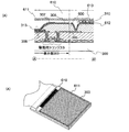
まず、従来の構造について図11を用いて説明する。100が基板、101が対向(封止)基板、102が表示部、103が外部接続部、105が駆動回路部、500が引き回し配線である。このように、従来の構造においては引き回し配線500があるために、表示部102が基板に比べてかなり小さくなってしまっている。
First, a conventional structure will be described with reference to FIG.
図1(A)は本発明を適用した電界発光ディスプレイに用いられるパネルである。基板100上に形成された電界発光素子を対向基板101で封止することによって表示部102が形成されている。103、104は外部接続部、105は駆動回路部である。なお、アノード線またはカソード線は表示部102に形成されており、それらの端部は外部接続部103及び104側にある。
FIG. 1A shows a panel used in an electroluminescent display to which the present invention is applied. The
このようにパネルの対向する2端(アノード線またはカソード線の端部に近い方)に外部接続部を設けてそれぞれ近い方の外部接続部より電圧を供給することで、従来と比較して表示部の面積を大きくしても、大きな電圧降下が起こらず、高品質な表示を得ることが可能となる。 In this way, an external connection is provided at the two opposite ends of the panel (closer to the end of the anode line or cathode line), and the voltage is supplied from the external connection of the closer side, so that display is possible in comparison with the conventional case. Even if the area of the portion is increased, a large voltage drop does not occur and a high-quality display can be obtained.
図1(B)、(C)は外部接続部103、104に接続する配線の例である。本実施の形態においてはフレキシブル配線基板(FPC等)106を用いて接続を行った例を示している。
1B and 1C show examples of wirings connected to the
図1(B)はトップエミッションの場合の例であり、フレキシブル配線基板106は基板の裏側を通って外部接続部104に接続している。この構造であると、外部接続部103と104に接続するフレキシブル配線基板106は1枚で済む。図1(C)は同様にボトムエミッションの例となっている。
FIG. 1B is an example in the case of top emission, and the
なお、外部接続部103、104の形成の仕方はこれに限らず、ストライプ状に形成されたアノード線もしくはカソード線の両端側に形成されていれば、図2に示すように外部接続部200、201を形成してもよいし、それらに接続する配線(この場合フレキシブル配線基板)は1枚ではなく、図2(B)に示すように2枚(202、203)でもかまわない。この場合、フレキシブル配線基板202と203両方が表示部102に係らないように接続されていれば、両面発光(デュアルエミッション)でも用いることが可能である。
Note that the method of forming the
なお、フレキシブル配線基板の代わりに図12(A)〜(C)のように導電性のリボン2001、2003を用いても良い。この場合は、図示した様にアノード線もしくはカソード線の一端にはフレキシブル配線基板2000、2006から電圧を供給し、もう一端に導電性のリボン2001、2003を介して電圧を供給する様にしても良いし、また、図14に示したように外部接続部2009と導電性のリボン2002をさらに設けてアノード線もしくはカソード線の両端に導電性のリボン2001、2002、2003から電圧を供給する様にしても良い。
Instead of the flexible wiring board,
図12(A)(B)において導電性のリボン2001は図1(A)〜(C)の外部接続部103、104に相当する外部接続部2007においてハンダや導電性の粘着剤など導電性を損なわない物によって適宜接着する。図12(A)は図1(B)に相当し、上面に光を取り出す構造の際に導電性のリボン2001で引き回し配線を代用した場合の図である。また図12(B)は図1(C)に相当し、下面に光を取り出す構造の際に導電性のリボン2001で引き回し配線を代用した場合の図である。また、図12(C)は図2(B)に相当し、図2(B)における外部接続部201に相当する外部接続部2008において導電性のリボン2003が電気的に接触しており、アノード線もしくはカソード線の一端に電圧を供給する。図12(C)におけるフレキシブル配線基板2006は図2(B)におけるフレキシブル配線基板202に相当する。
12A and 12B, the
導電性のリボン2001には、予め接着面に接着剤が塗布された市販の導電性テープ等を用いることも可能である。
For the
図13(A)、(B)はフレキシブル配線基板の代わりに導電線2004を用いた例である。この場合も図12(A)〜(C)と同様、アノード線もしくはカソード線の一端にはフレキシブル配線基板2000から電圧を供給し、もう一端に導電線2004を介して電圧を供給する様にしても良いし、図示はしていないが図14のように外部接続部と導電線をさらに設けてアノード線もしくはカソード線の両端に導電線より電圧を供給する様にしても良い。
FIGS. 13A and 13B show an example in which a
導電線2004は図1の外部接続部103、104に相当する外部接続部2005においてハンダなどによって適宜接着すればよい。図13(A)は図1(B)に相当し、上面に光を取り出す構造の際に導電線2004で引き回し配線を代用した場合の図である。また図13(B)は図1(C)に相当し、下面に光を取り出す構造の際に導電線2004で引き回し配線を代用した場合の図である。
The
なお、導電線2004は電気的な接触が必要である部分以外に絶縁被膜が形成されていても良いし、されていなくとも良い。導電線の材料に限定はないが、銅や銀、金、アルミニウムなどの抵抗の低いものでなることが望ましい。
Note that the
このように引き回し配線の代わりに導電性のリボン2001や導電線2004を用いても良い。また、その他の導電体を引き回し配線の代わりに用いても本発明の主旨に反しない限り適用可能であることは言うまでも無い。
In this way, a
(実施の形態2)
本実施の形態では引き回し配線を封止缶で代用する例について図3を参照しながら説明する。
(Embodiment 2)
In the present embodiment, an example of substituting the routing wiring with a sealing can will be described with reference to FIG.
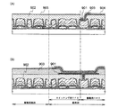
図3(A)の斜視図は本発明の構成を、封止缶を用いて実施した例である。基板300、フレキシブル配線基板301、封止缶302、表示部303、封止缶への電圧供給部304となっている。本構成においてはフレキシブル配線基板301側のアノード線またはカソード線の端部にはフレキシブル配線基板より電圧が供給され、フレキシブル配線基板301より遠い他端に封止缶を通して電圧が供給されている。
The perspective view of FIG. 3A is an example in which the structure of the present invention is implemented using a sealing can. A
図3(B)、(C)はアノード線またはカソード線へ封止缶302から電圧が供給されている部分(斜視図のA−A’)の断面図である。基板300上の表示領域に発光素子313を駆動する為の駆動用トランジスタ(Pチャネル型)が形成されており、そのソース側にアノード線が接続されている。この際、306は発光素子313の陽極、307は有機化合物を含む発光層、308は発光素子313の陰極となっている。本実施の形態では306は発光素子313の陽極となっているが、306が陰極である場合は、308が発光素子の陽極、305はカソード線、駆動用トランジスタはNチャネル型となるが大勢は同じと考えて良い。そしてこの表示部303の発光素子313を内側に乾燥剤311を取り付けた封止缶302で封止している。その後、絶縁性の膜314を封止缶上に成膜して、他部分からのショートなどを防いでいる。
3B and 3C are cross-sectional views of a portion (A-A ′ in the perspective view) where voltage is supplied from the sealing can 302 to the anode line or the cathode line. A driving transistor (P channel type) for driving the
310、312は封止剤である。310は絶縁性の封止剤を用いており、その内側で導線性の材料309でアノード線305と封止缶302の導通をとっている。導電性の材料309はアノード線305と封止缶302との導通がとれれば何でもかまわないが、導電性粒子を分散させた粘性のある液体をインクジェット法などで塗布したり、図4(A)のように土手と呼ばれる絶縁膜600にアノード線まで達する開口部601を形成し、その中にはんだボールなどの導電性粒子602を詰めたり、導電性粒子を分散させた液体を流し込んだり、図4(B)のように開口部601の中に導電性のフィラー603を立てたりしてアノード線と封止缶の導通を採ることが考えられる。導電性の材料309や導電性粒子602、フィラー603は弾性を有していると封止缶とアノード線との導通不良が起こりにくく好適である。また、封止材312は導電性の封止材であり、図3(C)のように封止材312を介してアノード線305と封止缶302との導通をとることができる。
310 and 312 are sealants. An insulating
また、図5(A)のように封止缶のアノード線との導通を取る部分に弾性を有するバネのようなもの700を取り付けて導通をとっても良い。もちろん、弾性を有するバネのようなもの700の形状は図5(A)に示した形状に限定されず、弾性を有し、アノード線もしくはカソード線と良好な導通がとれるような形状、材質であればどのようなものを用いてもかまわない。また、これと上記した導通方法と組み合わせるとさらに良い。
Further, as shown in FIG. 5A, an
封止缶302はステンレスなどが良く用いられるが、Ni/ステンレス鋼クラッドを用いると、接触抵抗が低くなり、加工性も良くなるので望ましい材料である。もちろんその他の材料であっても良好に水分など、電界発光素子に悪影響を及ぼす物質を防ぐ材料であり、本発明に利用できるような形に加工できるものであれば使用することが可能である。 Stainless steel or the like is often used for the sealing can 302. However, using Ni / stainless steel clad is a desirable material because the contact resistance is lowered and the workability is improved. Of course, other materials can be used as long as they are materials that can prevent moisture and other substances that adversely affect the electroluminescent element, and can be processed into a shape that can be used in the present invention.
また、アノード線またはカソード線の両端に封止缶から電圧を供給し、封止缶への電圧の供給を外部の電源回路より直接行えば、フレキシブル配線基板など外部接続部においてアノード線もしくはカソード線に電圧を供給するために占められていたピンを削減することができる。 Moreover, if voltage is supplied from the sealing can to both ends of the anode line or the cathode line, and the voltage is directly supplied to the sealing can from an external power supply circuit, the anode line or cathode line is connected to the external connection portion such as a flexible wiring board. The pins occupied to supply voltage can be reduced.
このように、封止缶302を引き回し配線の代わりにアノード線もしくはカソード線に電圧を供給する配線として使用することで、従来と比較して表示部の面積の割合を大きくしても、大きな電圧降下が起こらず、高品質な表示を得ることが可能となる。 As described above, the sealing can 302 is used as a wiring for supplying a voltage to the anode line or the cathode line in place of the wiring, so that a large voltage can be obtained even when the area ratio of the display portion is increased as compared with the conventional case. A descent does not occur, and a high-quality display can be obtained.
(実施の形態3)
本実施の形態では、本発明における他の構成について図6を参照しながら説明する。本実施の形態では引き回し配線の代わりとなる導電膜を対向基板に形成する例について説明する。
(Embodiment 3)
In this embodiment, another structure of the present invention will be described with reference to FIG. In this embodiment, an example in which a conductive film serving as a substitute for the lead wiring is formed over the counter substrate will be described.
対向基板は電界発光素子を形成した基板を紫外線硬化樹脂などによるシール剤で封止する際に使用する。シール剤と対向基板により封止されることで電界発光素子を外部の雰囲気から遮断することができ、信頼性の向上を図っている。 The counter substrate is used when the substrate on which the electroluminescent element is formed is sealed with a sealing agent such as an ultraviolet curable resin. By sealing with a sealing agent and a counter substrate, the electroluminescent element can be shielded from the external atmosphere, and reliability is improved.
本実施の形態では、対向基板に引き回し配線の代わりとなる導電膜を形成し、その導電膜に電圧を供給し、導電膜とアノード線もしくはカソード線の導通をはかることによってアノード線もしくはカソード線に電圧を供給する。 In this embodiment, a conductive film serving as a lead wiring is formed on the counter substrate, a voltage is supplied to the conductive film, and conduction between the conductive film and the anode line or the cathode line is achieved. Supply voltage.
対向基板に形成する導電膜の形状はどのような形状でもかまわないが、配線抵抗をなるべく小さくする為には膜厚方向へ切断したと考えた場合の断面積をなるべく大きく取ること、すなわち、膜厚をできるだけ大きく取ること、及びアノード線もしくはカソード線のストライプ形状に直交する方向における成膜範囲をなるべく大きく取ることが好ましい。 The shape of the conductive film formed on the counter substrate may be any shape, but in order to reduce the wiring resistance as much as possible, the cross-sectional area when taken in the film thickness direction is taken as large as possible, that is, the film It is preferable to make the thickness as large as possible and to make the film forming range as large as possible in the direction orthogonal to the stripe shape of the anode line or cathode line.
電界発光表示パネルには大きく分けて3つの表示方法、すなわち素子を形成した基板側に光を射出する底面発光、対向基板側に光を射出する上面発光及びその両方に光を射出する両面発光がある。 The electroluminescent display panel is roughly divided into three display methods, namely, bottom emission for emitting light to the substrate side on which the element is formed, top emission for emitting light to the opposite substrate side, and double-sided emission for emitting light to both. is there.
底面発光の場合は素子を形成した基板側に光が出るので、対向基板に形成する引き回し配線の代わりとなる導電膜は透光性を有していなくてもかまわない。アルミニウムや銀など、形成しやすく導電率の高い材料を適宜用いることが可能である。 In the case of bottom emission, light is emitted to the substrate side on which the element is formed. Therefore, the conductive film serving as a substitute for the lead wiring formed on the counter substrate may not have a light-transmitting property. A material that can be easily formed and has high conductivity, such as aluminum or silver, can be used as appropriate.
しかし、上面発光や両面発光では対向基板の方に光が出るため、対向基板に形成する引き回し配線の代わりとなる導電膜には透光性が求められる。透光性を有し且つ導電性も有する材料としては、ITO(indium tin oxide)、酸化インジウムに2〜20%の酸化亜鉛(ZnO)を混合したIZO(indium zinc oxide)、酸化インジウムに2〜20%の酸化珪素(SiO2)を混合したITSOなどが挙げられる。これらの材料に限らず、使用に十分である透光性と導電率を有する材料であればどのような材料を用いてもかまわない。 However, in the case of top emission or double-sided emission, light is emitted toward the counter substrate. Therefore, the conductive film serving as a substitute for the lead wiring formed on the counter substrate is required to have translucency. As a material having translucency and conductivity, ITO (indium tin oxide), IZO (indium zinc oxide) in which 2 to 20% zinc oxide (ZnO) is mixed with indium oxide, and 2 to indium oxide are used. ITSO mixed with 20% silicon oxide (SiO 2 ) can be used. Not limited to these materials, any material may be used as long as the material has translucency and conductivity sufficient for use.
対向基板に形成された導電膜とアノード線もしくはカソード線を接続する方法としては、実施の形態2と同様の方法、もしくは公知の方法で接続すればよく実施者の判断にゆだねられる所である。一例として図6に接続を行った様子を示した。対向基板610に形成された導電膜611には外部電源回路より電圧が供給されている。駆動用トランジスタに接続されているアノード線305には土手と呼ばれる絶縁膜600に形成されたコンタクトを介して電界発光素子313の陽極を形成すると同時に引き出し配線612を形成する。引き出し配線612は導電膜611と導電性を有する粒子613を介して接続され、アノード線305に導電膜611から電圧が供給される。
As a method for connecting the conductive film formed on the counter substrate to the anode line or the cathode line, the connection may be made by the same method as in the second embodiment or a known method, which is left to the judgment of the practitioner. As an example, FIG. 6 shows the connection. A voltage is supplied to the
このように、対向基板610に形成された導電膜611を引き回し配線の代わりにアノード線もしくはカソード線に電圧を供給する配線として使用することで、従来と比較して表示部の面積の割合を大きくしても、大きな電圧降下が起こらず、高品質な表示を得ることが可能となる。
In this manner, the
また、図15に示すように引き回し配線の代わりに用いられる導電膜は対向基板101における基板100側の面のみでは無く、基板100における素子が形成されている面と反対の面、もしくは、図示していないが、対向基板101の基板100と反対の面に形成されていても良い。形状や材料に関する条件は導電膜を対向基板の内側に形成する場合と同様である。この場合、導電膜をアノード線もしくはカソード線に接続するには、図のように基板に貫通孔155を設ける。この貫通孔155を設けることによって、導電膜151を成膜する際に、導電膜151を成膜する基板の面の反対側の面に導電膜151の材料が回り込み、基板の反対側において導通を取ることができるようになる。また、実施の形態1で挙げたような導電性のリボンや導電性テープなどにより導通を得ても良い。
Further, as shown in FIG. 15, the conductive film used in place of the routing wiring is not only the surface of the
なお、図15において、導電膜151にはフレキシブル配線基板150によって電圧を供給しているが、導電膜151に電圧を供給する方法に関してはこれに限らず、フレキシブル配線基板ではなくとも何らかの導電体により所望の電圧が供給されていればよい。なお、対向基板101と基板100はシール材154により固着されており、導電膜151によって供給された電圧は引き込み配線152により、表示部153のアノード線もしくはカソード線に供給される。
In FIG. 15, a voltage is supplied to the
(実施の形態4)
本実施の形態では、アノード線もしくはカソード線へ電圧を供給する配線について、簡単に図7を用いて説明する。400は画素部であり、複数のアノード線もしくはカソード線がストライプ状に形成されている。アノード線もしくはカソード線はその一端が一本の配線に全て接続されており、他端ももう一本の配線に全て接続されている。また、図7ではアノード線もしくはカソード線への入力に関係のある配線のみを示した図である。
(Embodiment 4)
In this embodiment mode, wiring for supplying a voltage to an anode line or a cathode line will be briefly described with reference to FIG.
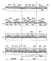
図7(A)は従来の引き回し配線が形成されているパネルの配線図である。400に画素部のアノード線、もしくはカソード線がストライプ状に形成されている。アノード線、もしくはカソード線の端部はフレキシブル配線基板などの外部接続部側とその対辺側にあり、それぞれ外部接続部より電圧が供給されている。外部接続部の対辺側には401の引き回し配線部を通って、引き回し配線が接続されているが、電圧降下の影響を防ぐため、その幅は大きく取らなければいけない。そのため、画素部として使用できる領域が狭くなってしまっている。
FIG. 7A is a wiring diagram of a panel on which a conventional lead wiring is formed. In 400, anode lines or cathode lines of the pixel portion are formed in a stripe shape. The ends of the anode line or the cathode line are on the external connection part side such as a flexible wiring board and the opposite side, and a voltage is supplied from the external connection part. The lead wire is connected to the opposite side of the external connection portion through the
図7(B)は本発明の構成の一つを用いて構成されているパネルである。アノード線またはカソード線の両端側に外部接続部が設けられており、各々近い方の外部接続部から電圧が供給されている。引き回し配線部が不要となるため、表示部の面積の割合が多くなっているのがわかる。また、フレキシブル配線基板などあまり線幅に制約のない配線を用いて電圧を供給しているため、電圧降下の心配もない。これにより、額縁面積の小さな、高画質のディスプレイを作製することが可能となる。 FIG. 7B illustrates a panel formed using one of the structures of the present invention. External connection portions are provided on both ends of the anode line or the cathode line, and a voltage is supplied from the external connection portions closer to each other. It can be seen that the proportion of the area of the display portion is increased because the lead-out wiring portion is unnecessary. In addition, since the voltage is supplied using a wiring such as a flexible wiring board that does not have a very limited line width, there is no fear of a voltage drop. As a result, a high-quality display with a small frame area can be manufactured.
図7(C)は本発明の構成の一つを用いて構成されているパネルである。外部接続部が設けられた側のアノード線またはカソード線の端部は外部接続部から電圧が供給され、他端には封止缶もしくは対向基板に形成された導電膜を用いて電圧を供給している。402は封止缶もしくは対向基板に形成された導電膜より電圧が供給される部分である。引き回し配線部が不要となるため、表示部の面積の割合が多くなっているのがわかる。また、断面積の大きい封止缶もしくは対向基板に形成された導電膜を配線として用いて電圧を供給しているため、電圧降下の心配も少ない。これにより、額縁面積の小さな、高画質のディスプレイを作製することが可能となる。
FIG. 7C illustrates a panel formed using one of the structures of the present invention. A voltage is supplied from the external connection part to the end of the anode line or cathode line on the side where the external connection part is provided, and a voltage is supplied to the other end using a conductive film formed on a sealing can or a counter substrate. ing.
図7(D)は本発明の構成の一つを用いて構成されているパネルである。アノード線またはカソード線の両端に封止缶もしくは対向基板に形成された導電膜を用いて電圧を供給している。402は封止缶もしくは対向基板に形成された導電膜より電圧が供給される部分である。引き回し配線部が不要となるため、表示部の面積の割合が多くなっているのがわかる。また、断面積の大きい封止缶もしくは対向基板に形成された導電膜を配線として用いて電圧を供給しているため、電圧降下の心配もない。さらに、外部接続部より、アノード線もしくはカソード線に電圧を供給しないことになるためピン数の節約になり、レイアウトが楽になったり、他の有用な情報をパネル内に供給することができるようになる。これにより、額縁面積の小さな、高画質のディスプレイを作製することが可能となる。
FIG. 7D illustrates a panel formed using one of the structures of the present invention. A voltage is supplied using a conductive film formed on a sealing can or a counter substrate at both ends of the anode line or the cathode line.
本実施例では、本発明を使用して薄膜トランジスタ及び容量、そして電界発光装置を作製する方法について図8〜図9を参照しながら説明する。 In this embodiment, a method for manufacturing a thin film transistor, a capacitor, and an electroluminescent device using the present invention will be described with reference to FIGS.
まず、基板800上に下地絶縁膜801を形成してから非晶質半導体膜を成膜し、結晶化を促進する元素を用いて結晶化することで結晶質半導体膜とする。
First, after forming the
基板800としてはガラス基板、石英基板、結晶性ガラスなどの絶縁性基板や、セラミック基板、ステンレス基板、金属基板(タンタル、タングステン、モリブデン等)、半導体基板、プラスチック基板(ポリイミド、アクリル、ポリエチレンテレフタレート、ポリカーボネート、ポリアリレート、ポリエーテルスルホン等)等を用いることができるが、少なくともプロセス中に発生する熱に絶えうる材料を使用する。本実施例においてはガラス基板を使用する。
As the
下地絶縁膜801は基板800中のアルカリ金属やアルカリ土類金属が、結晶性ケイ素膜中に拡散するのを防ぐ為に設ける。このような元素は結晶性ケイ素膜の半導体特性に悪影響をおよぼしてしまうためである。材料としては酸化ケイ素、窒化ケイ素、窒化酸化ケイ素及び窒化酸化ケイ素などを用いることができ、単層または積層構造とすることにより形成する。なお、アルカリ金属やアルカリ土類金属の拡散の心配のない基板であれば特に下地絶縁膜は設ける必要がない。
The base
本実施例においては下地絶縁膜801は積層構造により作製し、1層目の絶縁膜として窒化酸化ケイ素膜を50nm、2層目の絶縁膜として酸化窒化ケイ素膜を100nmで形成した。なお、窒化酸化ケイ素膜と酸化窒化ケイ素膜はその窒素と酸素の割合が異なっていることを意味しており、前者の方がより窒素の含有量が高いことを示している。1層目の下地膜は、プラズマCVD法により、原料ガスにSiH4、N2O、NH3、H2を使用し、圧力が0.3Torr、RFパワーが50W、RF周波数が60MHz、基板温度が400℃として形成する。2層目の下地膜は同じくプラズマCVD法により、原料ガスにSiH4、N2Oを用い、圧力が0.3Torr、RFパワーが150W、RF周波数が60MHz、基板温度が400度の条件で形成する。
In this embodiment, the
続いて下地絶縁膜上に非晶質半導体膜を形成する。本実施例においては非晶質ケイ素膜を25〜100nm(好ましくは30〜60nm)の膜厚で形成する。作製方法としては、公知の方法、例えばスパッタ法、減圧CVD法、またはプラズマCVD法等が使用できる。本実施例では、プラズマCVD法により膜厚50nmに形成する。 Subsequently, an amorphous semiconductor film is formed over the base insulating film. In this embodiment, an amorphous silicon film is formed with a thickness of 25 to 100 nm (preferably 30 to 60 nm). As a manufacturing method, a known method such as a sputtering method, a low pressure CVD method, or a plasma CVD method can be used. In this embodiment, the film is formed to a thickness of 50 nm by plasma CVD.
続いて非晶質半導体膜の結晶化を行う。結晶化は非晶質半導体膜の結晶化を促進する元素を用い、加熱処理を行うことによって行う。結晶化を促進する元素とは、代表的にはニッケルが挙げられ、このような元素を用いることによって用いない場合に比べて低温、短時間で結晶化が行われるためガラス基板など比較的熱に弱い基板を使用する際に好適に用いることが可能である。このような結晶化を促進する元素としては、ニッケルの他に鉄、パラジウム、スズ、鉛、コバルト、白金、銅、金などがある。この中から一種もしくは複数種を用いればよい。 Subsequently, the amorphous semiconductor film is crystallized. Crystallization is performed by performing heat treatment using an element that promotes crystallization of the amorphous semiconductor film. An example of an element that promotes crystallization is nickel. By using such an element, crystallization is performed at a lower temperature and in a shorter time than when not used. It can be suitably used when a weak substrate is used. Examples of such elements that promote crystallization include iron, palladium, tin, lead, cobalt, platinum, copper, and gold in addition to nickel. One or more of these may be used.
このような元素の添加方法としては、例えばこのような元素の塩を溶媒に溶かしてスピンコート法やディップ法などで塗布する方法がある。溶媒としては有機溶媒や水などが使用できるが、半導体膜上に直接触れるため、半導体特性に悪影響を及ぼさないものを選ぶことが肝要である。また、塩についても同様である。 As an addition method of such an element, for example, there is a method in which a salt of such an element is dissolved in a solvent and applied by a spin coating method or a dip method. As the solvent, an organic solvent, water, or the like can be used, but it is important to select a solvent that does not adversely affect the semiconductor characteristics because it directly touches the semiconductor film. The same applies to the salt.
本実施例では、結晶化を促進する元素としてNiを用いる場合の一例を紹介する。Niは酢酸塩や硝酸塩を10ppm水溶液として用いると良い。この水溶液をスピンコート法により非晶質ケイ素膜上に塗布するのだが、ケイ素膜の表面は疎水性であるために均一に塗布できない可能性があるので、あらかじめオゾン水などで非晶質ケイ素膜表面を処理し、極薄い酸化膜を形成しておくことが好ましい。 In this embodiment, an example of using Ni as an element for promoting crystallization will be introduced. Ni is good to use acetate and nitrate as 10ppm aqueous solution. This aqueous solution is applied onto the amorphous silicon film by spin coating, but the surface of the silicon film is hydrophobic and may not be uniformly applied. It is preferable to treat the surface to form an extremely thin oxide film.
結晶化を促進する元素の非晶質ケイ素膜への導入方法としては他にイオン注入法、Niを含有する水蒸気雰囲気中での加熱、ターゲットをNi材料としてのスパッタリングなどが考えられる。 Other methods for introducing an element that promotes crystallization into an amorphous silicon film include ion implantation, heating in a water vapor atmosphere containing Ni, and sputtering using a Ni material as a target.
次いで、加熱処理を行い、非晶質半導体膜を結晶化させる。本実施例では非晶質ケイ素膜を結晶化するために触媒元素を用い、500〜650度で2〜24時間程度加熱処理を行えばよい。この結晶化処理により、非晶質ケイ素膜は結晶質ケイ素膜となる。この際、磁場をかけて、その磁気エネルギーと合わせて結晶化させてもよいし、高出力マイクロ波を使用しても構わない。本実施例では、非晶質ケイ素膜に縦型炉を用いて500℃で1時間熱処理後、550度で4時間熱処理を行うことで結晶質ケイ素膜が形成される。 Next, heat treatment is performed to crystallize the amorphous semiconductor film. In this embodiment, a catalytic element is used to crystallize the amorphous silicon film, and heat treatment may be performed at 500 to 650 degrees for about 2 to 24 hours. By this crystallization treatment, the amorphous silicon film becomes a crystalline silicon film. At this time, a magnetic field may be applied to crystallize with the magnetic energy, or a high-power microwave may be used. In this embodiment, the amorphous silicon film is heat-treated at 500 ° C. for 1 hour using a vertical furnace, and then heat-treated at 550 ° C. for 4 hours to form a crystalline silicon film.
続いて、レーザによる結晶化を行っても良い。結晶質半導体膜中の欠陥を低減させることにより結晶性を向上させる。レーザ結晶化法は、レーザ発振装置として、パルス発振型、または連続発振型の気体または固体及び金属レーザ発振装置を用いれば良い。気体レーザとしては、エキシマレーザ、Arレーザ、Krレーザ等があり、固体レーザとしては、YAGレーザ、YVO4レーザ、YLFレーザ、YAlO3レーザ、ガラスレーザ、ルビーレーザ、アレキサンドライドレーザ、サファイアレーザ、金属レーザとしては、ヘリウムカドミウムレーザ、銅蒸気レーザ、金蒸気レーザが挙げられるなどがある。固体レーザのレーザ媒質である結晶には、Cr3+、Cr4+、Nd3+、Er3+、Ce3+、Co2+、Ti3+、Yb3+又は、V3+から選択される一種又は複数種が不純物としてドープされている。 Subsequently, crystallization with a laser may be performed. Crystallinity is improved by reducing defects in the crystalline semiconductor film. In the laser crystallization method, a pulse oscillation type or continuous oscillation type gas or solid and metal laser oscillation device may be used as a laser oscillation device. Examples of gas lasers include excimer laser, Ar laser, Kr laser, and solid-state lasers include YAG laser, YVO 4 laser, YLF laser, YAlO 3 laser, glass laser, ruby laser, alexandride laser, sapphire laser, metal Examples of the laser include a helium cadmium laser, a copper vapor laser, and a gold vapor laser. The crystal which is the laser medium of the solid laser is selected from Cr 3+ , Cr 4+ , Nd 3+ , Er 3+ , Ce 3+ , Co 2+ , Ti 3+ , Yb 3+ or V 3+ One or more species are doped as impurities.
レーザ発振装置により発振されたレーザは光学系を用いて線状にして照射を行うと好ましい。線状レーザは通常用いられるシリンドリカルレンズや凹型を有するミラーなどを用いることで得ることができる。照射条件としては、パワー密度が0.01〜100MW/cm2程度、照射雰囲気としては大気、または酸素濃度を制御した雰囲気、N2雰囲気または真空中が挙げられる。また、パルス発振のレーザを用いる場合には、周波数30〜300Hzとし、レーザエネルギー密度を100〜1500mJ/cm2(代表的には200〜500mJ/cm2)とするのが望ましい。このとき、レーザ光をレーザビームのFWHMで計算して50〜98%オーバーラップさせても良い。なお、本実施例において結晶化雰囲気は大気中とする。 The laser oscillated by the laser oscillation device is preferably irradiated in a linear form using an optical system. The linear laser can be obtained by using a commonly used cylindrical lens or a concave mirror. Examples of the irradiation conditions include a power density of about 0.01 to 100 MW / cm 2 , and examples of the irradiation atmosphere include air, an atmosphere with a controlled oxygen concentration, an N 2 atmosphere, or a vacuum. When a pulsed laser is used, it is desirable that the frequency be 30 to 300 Hz and the laser energy density be 100 to 1500 mJ / cm 2 (typically 200 to 500 mJ / cm 2 ). At this time, the laser light may be calculated by the FWHM of the laser beam and overlapped by 50 to 98%. In this embodiment, the crystallization atmosphere is air.
本実施例において大気中でレーザー照射を行うと、結晶質ケイ素膜上に自然酸化膜である酸化ケイ素膜が形成される。この膜質は制御できないため、除去してしまうことが望ましい。 In this embodiment, when laser irradiation is performed in the atmosphere, a silicon oxide film, which is a natural oxide film, is formed on the crystalline silicon film. Since this film quality cannot be controlled, it is desirable to remove it.
この場合はフッ素を含む液と界面活性を示す物質が含まれた液との混合液を用いると下層の結晶質ケイ素膜中にニッケル及び/又はニッケルシリサイドの偏析があったとしても、酸化ケイ素膜のみを選択性良くエッチングできるため、結晶質ケイ素膜に孔が発生することが抑制される。 In this case, if a mixed liquid of a liquid containing fluorine and a liquid containing a substance exhibiting surface activity is used, even if there is segregation of nickel and / or nickel silicide in the lower crystalline silicon film, the silicon oxide film Therefore, the generation of pores in the crystalline silicon film is suppressed.
次に結晶質半導体膜上に酸化ケイ素膜を形成する。酸化ケイ素膜は酸素雰囲気中でのUV光の照射、熱酸化法、ヒドロキシラジカルを含むオゾン水又は過酸化水素による処理等により形成する。次いでスパッタ法YCVD法にてゲッタリングサイトを形成する。スパッタで形成するときはゲッタリングサイトはアルゴン元素を含む非晶質ケイ素膜を膜厚50nm堆積することで形成する。成膜条件は、成膜圧力:0.3Pa、ガス(Ar)流量:50(sccm)、成膜パワー:3kW、基板温度:150℃とした。なお、上記条件での非晶質ケイ素膜に含まれるアルゴン元素の原子濃度は、3×10²⁰/cm3〜6×1020/cm3、酸素の原子濃度は1×1019/cm3〜3×1019/cm3程度である。その後、ラピッドアニール装置を用いて650℃、3分の加熱処理を行いゲッタリングする。 Next, a silicon oxide film is formed on the crystalline semiconductor film. The silicon oxide film is formed by irradiation with UV light in an oxygen atmosphere, a thermal oxidation method, treatment with ozone water containing hydrogen radicals or hydrogen peroxide, and the like. Next, gettering sites are formed by sputtering YCVD. When formed by sputtering, the gettering site is formed by depositing an amorphous silicon film containing an argon element to a thickness of 50 nm. The film formation conditions were film formation pressure: 0.3 Pa, gas (Ar) flow rate: 50 (sccm), film formation power: 3 kW, and substrate temperature: 150 ° C. Note that the atomic concentration of argon element contained in the amorphous silicon film under the above conditions is 3 × 10 20 / cm 3 to 6 × 10 20 / cm 3 , and the atomic concentration of oxygen is 1 × 10 19 / cm 3 to It is about 3 × 10 19 / cm 3 . Then, gettering is performed by performing a heat treatment at 650 ° C. for 3 minutes using a rapid annealing apparatus.
加熱処理を行うことで結晶質半導体膜中の結晶化を促進する元素の少なくとも一部をゲッタリングサイトに移動する。この際の加熱処理によりゲッタリングサイト上には酸化ケイ素膜よりなる自然酸化膜が形成されている。 By performing the heat treatment, at least part of the element that promotes crystallization in the crystalline semiconductor film is moved to the gettering site. By this heat treatment, a natural oxide film made of a silicon oxide film is formed on the gettering site.
この後、フッ素と界面活性を示す物質を含む液により、自然酸化膜を除去し、ゲッタリングサイトをTMAH(Tetra methyl ammonium hydroxide)含有水溶液を用いて60度程度に加熱し、エッチングする。 Thereafter, the natural oxide film is removed with a liquid containing fluorine and a substance exhibiting surface activity, and the gettering site is heated to about 60 degrees using a TMAH (Tetra methyl ammonium hydroxide) -containing aqueous solution and etched.
その後、ゲッタリングサイトをエッチングする際にエッチングストッパーとして用いた酸化ケイ素膜をフッ素と界面活性を示す物質を含む液でエッチングし、除去する。エッチングストッパー膜として用いられた酸化ケイ素膜中にはニッケルが多量に含まれている可能性があり、その後の処理を行うことで活性層が汚染される心配もあるため、除去することが望ましい。 Thereafter, the silicon oxide film used as an etching stopper when the gettering site is etched is removed by etching with a liquid containing fluorine and a substance having surface activity. The silicon oxide film used as the etching stopper film may contain a large amount of nickel, and the subsequent treatment may cause contamination of the active layer.
続いて、結晶質半導体膜に必要に応じてしきい値をコントロールするための微量の不純物を添加する、いわゆるチャネルドーピングを行う。要求されるしきい値を得るために、ボロンもしくはリン等をイオンドーピング法などにより添加する。 Subsequently, so-called channel doping is performed in which a trace amount of impurities for controlling the threshold is added to the crystalline semiconductor film as necessary. In order to obtain a required threshold value, boron or phosphorus is added by an ion doping method or the like.
その後、図8(A)に示すように、所定の形状にパターニングし、島状の結晶性半導体層801a〜801dを得る。パターニングは、結晶質半導体膜にフォトレジストを塗布し、所定の形状を有するマスクを用いて露光し、焼成して、結晶質半導体膜上にマスクを形成し、このマスクを用いて、ドライエッチング法により結晶質半導体膜をエッチングすることで行われる。ドライエッチング法のガスは、CF4と、O2等を用いて行えば良い。
After that, as shown in FIG. 8A, patterning is performed in a predetermined shape to obtain island-shaped
続いて、結晶性半導体層801a〜801dを覆うようにゲート絶縁膜822を形成する。ゲート絶縁膜822はプラズマCVD法またはスパッタ法を用い膜厚を40〜150nmとしてケイ素を含む絶縁膜で形成する。本実施例では、ゲート絶縁膜822はプラズマCVD法により酸化窒化珪素膜を115nmの厚さに形成する。
Subsequently, a
次いで、ゲート絶縁膜上に第1の導電層802として膜厚30nmの窒化タンタル(TaN)とその上に第2の導電層803として膜厚370nmのタングステン(W)を形成する。TaN膜、W膜共スパッタ法で形成すればよく、TaN膜はTaのターゲットを用いて窒素雰囲気中で、W膜はWのターゲットを用いて成膜すれば良い。
Next, tantalum nitride (TaN) with a thickness of 30 nm is formed as a first
なお、本実施例では第1の導電層を膜厚30nmのTaN、第2の導電層を膜厚370nmのWとしたが、第1の導電層と第2の導電層は共にTa、W、Ti、Mo、Al、Cu、Cr、Ndから選ばれた元素、または前記元素を主成分とする合金材料若しくは化合物材料で形成してもよい。また、リン等の不純物元素をドーピングした多結晶珪素膜に代表される半導体膜を用いてもよい。また、AgPdCu合金を用いてもよい。さらに、その組み合わせも適宜選択すればよい。膜厚は第1の導電層が20〜100nm、第2の導電層が100〜400nmの範囲で形成すれば良い。また、本実施例では、2層の積層構造としたが、1層としてもよいし、もしくは3層以上の積層構造としてもよい。 In this embodiment, the first conductive layer is TaN having a thickness of 30 nm and the second conductive layer is W having a thickness of 370 nm. However, the first conductive layer and the second conductive layer are both Ta, W, You may form with the element chosen from Ti, Mo, Al, Cu, Cr, Nd, or the alloy material or compound material which has the said element as a main component. Alternatively, a semiconductor film typified by a polycrystalline silicon film doped with an impurity element such as phosphorus may be used. Further, an AgPdCu alloy may be used. Furthermore, the combination may be selected as appropriate. The film thickness may be in the range of 20 to 100 nm for the first conductive layer and 100 to 400 nm for the second conductive layer. In this embodiment, a two-layer structure is used, but a single layer may be used, or a three-layer or more structure may be used.
次に、前記導電層をエッチングして電極及び配線を形成するため、フォトリソグラフィーにより露光工程を経てレジストからなるマスクを形成する。第1のエッチング処理では第1のエッチング条件と第2のエッチング条件でエッチングを行う。レジストによるマスクを用い、エッチングし、ゲート電極及び配線を形成する。エッチング条件は適宜選択すれば良い。 Next, in order to form the electrode and the wiring by etching the conductive layer, a mask made of a resist is formed through an exposure process by photolithography. In the first etching process, etching is performed under the first etching condition and the second etching condition. Etching is performed using a resist mask to form gate electrodes and wirings. Etching conditions may be selected as appropriate.
本実施例では、ICP(Inductively Coupled Plasma:誘導結合プラズマ)エッチング法を使用した。第1のエッチング条件として、エッチング用ガスにCF4、Cl2とO2を用い、それぞれのガス流量比を25/25/10(sccm)とし、1.0Paの圧力でコイル型電極に500WのRF(13.56MHz)電力を投入してプラズマを生成してエッチングを行う。基板側(試料ステージ)にも150WのRF(13.56MHz)電力を投入し、実質的に負の自己バイアス電圧を印加する。この第1のエッチング条件によりW膜をエッチングして第1の導電層の端部をテーパー形状とする。 In this example, an ICP (Inductively Coupled Plasma) etching method was used. As the first etching conditions, CF 4 , Cl 2 and O 2 are used as etching gases, the respective gas flow ratios are set to 25/25/10 (sccm), and 500 W is applied to the coil-type electrode at a pressure of 1.0 Pa. Etching is performed by applying RF (13.56 MHz) power to generate plasma. 150 W RF (13.56 MHz) power is also applied to the substrate side (sample stage), and a substantially negative self-bias voltage is applied. The W film is etched under this first etching condition so that the end portion of the first conductive layer is tapered.
続いて、第2のエッチング条件に移ってエッチングを行う。レジストからなるマスクをのこしたまま、エッチング用ガスにCF4とCl2を用い、それぞれのガス流量比を30/30(sccm)、圧力1.0Paでコイル型の電極に500WのRF(13.56MHz)電力を投入してプラズマを生成して約15秒程度のエッチングを行う。基板側(試料ステージ)にも20WのRF(13.56MHz)電力を投入し、実質的に負の自己バイアス電圧を印加する。CF4とCl2を混合した第2のエッチング条件ではW膜及びTaN膜とも同程度にエッチングされる。なお、ゲート絶縁膜上に残渣を残すことなくエッチングするためには、10〜20%程度の割合でエッチング時間を増加させると良い。この第1のエッチング処理において、電極に覆われていないゲート絶縁膜は20nm〜50nm程度エッチングされ、基板側に印加されたバイアス電圧の効果により第1の導電層及び第2の導電層の端部はテーパー状となる。 Subsequently, the etching is performed under the second etching condition. With the mask made of resist applied, CF 4 and Cl 2 are used as etching gases, the respective gas flow ratios are 30/30 (sccm), the pressure is 1.0 Pa, and 500 W RF (13 .56 MHz) Electric power is applied to generate plasma, and etching is performed for about 15 seconds. 20 W RF (13.56 MHz) power is also applied to the substrate side (sample stage), and a substantially negative self-bias voltage is applied. Under the second etching condition in which CF 4 and Cl 2 are mixed, the W film and the TaN film are etched to the same extent. Note that in order to perform etching without leaving a residue on the gate insulating film, it is preferable to increase the etching time at a rate of about 10 to 20%. In this first etching process, the gate insulating film not covered with the electrode is etched by about 20 nm to 50 nm, and the end portions of the first conductive layer and the second conductive layer are applied by the effect of the bias voltage applied to the substrate side. Becomes tapered.
次いで、レジストからなるマスクを除去せずに第2のエッチング処理を行う。第2のエッチング処理では、エッチング用のガスにSF6とCl2とO2を用い、それぞれのガス流量比を24/12/24(sccm)とし、1.3Paの圧力でコイル型の電極に700WのRF(13.56MHz)電力を投入してプラズマを発生して25秒程度エッチングを行う。基板側(試料ステージ)にも10WのRF(13.56MHz)電力を投入し、実質的に負の自己バイアス電圧を印加した。このエッチング条件ではW膜が選択的にエッチングされ、第2形状の導電層を形成した。このとき第1の導電層はほとんどエッチングされない。第1、第2のエッチング処理によって第1の導電層802a〜802d、第2の導電層803a〜803dよりなるゲート電極が形成される。
Next, a second etching process is performed without removing the resist mask. In the second etching process, SF 6 , Cl 2, and O 2 are used as etching gases, the gas flow ratios are 24/12/24 (sccm), and a coil-type electrode is applied at a pressure of 1.3 Pa. 700 W RF (13.56 MHz) power is applied to generate plasma, and etching is performed for about 25 seconds. 10 W RF (13.56 MHz) power was also applied to the substrate side (sample stage), and a substantially negative self-bias voltage was applied. Under this etching condition, the W film was selectively etched to form a second shape conductive layer. At this time, the first conductive layer is hardly etched. A gate electrode including the first
そして、レジストからなるマスクを除去せず、第1のドーピング処理を行う。これにより、結晶性半導体層にN型を付与する不純物が低濃度に添加される。第1のドーピング処理はイオンドープ法又はイオン注入法で行えば良い。イオンドープ法の条件はドーズ量が1×10¹³〜5×10¹⁴atoms/cm2、加速電圧が40〜80kVで行えばよい。本実施例では加速電圧を50kVとして行った。N型を付与する不純物元素としては15族に属する元素を用いることができ、代表的にはリン(P)または砒素(As)が用いられる。本実施例ではリン(P)を使用した。その際、第1の導電層をマスクとして、自己整合的に低濃度の不純物が添加されている第1の不純物領域(N--領域)を形成した。 Then, the first doping process is performed without removing the resist mask. Thereby, an impurity imparting N-type is added to the crystalline semiconductor layer at a low concentration. The first doping process may be performed by an ion doping method or an ion implantation method. The ion doping method may be performed at a dose of 1 × 10 13 to 5 × 10 14 atoms / cm 2 and an acceleration voltage of 40 to 80 kV. In this embodiment, the acceleration voltage is 50 kV. As the impurity element imparting N-type, an element belonging to Group 15 can be used, and typically phosphorus (P) or arsenic (As) is used. In this example, phosphorus (P) was used. At that time, the first conductive layer as a mask, a first impurity region self-aligned manner low concentration impurity is added - to form a (N region).
続き、レジストからなるマスクを除去する。そして新たにレジストからなるマスクを形成して第1のドーピング処理よりも高い加速電圧で、第2のドーピング処理を行う。第2のドーピング処理もN型を付与する不純物を添加する。イオンドープ法の条件はドーズ量を1×10¹³〜3×10¹⁵atoms/cm2、加速電圧を60〜120kVとすれば良い。本実施例ではドーズ量を3.0×1015atoms/cm2とし、加速電圧を65kVとして行った。第2のドーピング処理は第2の導電層を不純物元素に対するマスクとして用い、第1の導電層の下方に位置する半導体層にも不純物元素が添加されるようにドーピングを行う。 Subsequently, the resist mask is removed. Then, a new mask made of resist is formed, and the second doping process is performed at a higher acceleration voltage than the first doping process. In the second doping process, an impurity imparting N-type is added. The conditions for the ion doping method may be that the dose is 1 × 10 13 to 3 × 10 15 atoms / cm 2 and the acceleration voltage is 60 to 120 kV. In this embodiment, the dose is set to 3.0 × 10 15 atoms / cm 2 and the acceleration voltage is set to 65 kV. In the second doping treatment, the second conductive layer is used as a mask for the impurity element, and doping is performed so that the impurity element is also added to the semiconductor layer located below the first conductive layer.
第2のドーピングを行うと、結晶質半導体層の第1の導電層と重なっている部分のうち、第2の導電層に重なっていない部分もしくはマスクに覆われていない部分に、第2の不純物領域(N-領域)が形成される。第2の不純物領域には1×10¹⁸〜5×10¹⁹atoms/cm3の濃度範囲でN型を付与する不純物が添加される。また、結晶質半導体層のうち、第1形状の導電層にもマスクにも覆われておらず、露出している部分(第3の不純物領域:N+領域)には1×1019〜5×1021atom/cm3の範囲で高濃度にN型を付与する不純物が添加される。また、半導体層にはN+領域が存在するが、一部マスクのみに覆われている部分がある。この部分のN型を付与する不純物の濃度は、第1のドーピング処理で添加された不純物濃度のままであるので、引き続き第1の不純物領域(N--領域)と呼ぶことにする。 When the second doping is performed, a portion of the crystalline semiconductor layer that overlaps the first conductive layer does not overlap with the second conductive layer or a portion that is not covered with the mask. A region (N − region) is formed. An impurity imparting N-type is added to the second impurity region in a concentration range of 1 × 10 18 to 5 × 10 19 atoms / cm 3 . Further, in the crystalline semiconductor layer, the exposed portion (third impurity region: N + region) which is not covered with the first shape conductive layer or the mask and is exposed to 1 × 10 19 to 5 Impurities imparting N-type are added at a high concentration in the range of × 10 21 atoms / cm 3 . In addition, the semiconductor layer has an N + region, but there is a portion that is partially covered only by the mask. The concentration of impurity imparting N-type in this portion, since the remains of the impurity concentration added in the first doping process, subsequently the first impurity regions - is referred to as (N region).
なお、本実施例では2回のドーピング処理により各不純物領域を形成したが、これに限定されることは無く、適宜条件を設定して、一回もしくは複数回のドーピングによって所望の不純物濃度を有する不純物領域を形成すれば良い。 In this embodiment, each impurity region is formed by two doping processes, but the present invention is not limited to this, and a desired impurity concentration is obtained by performing doping once or a plurality of times by appropriately setting conditions. An impurity region may be formed.
次いで、レジストからなるマスクを除去した後、新たにレジストからなるマスクを形成し、第3のドーピング処理を行う。第3のドーピング処理により、Pチャネル型TFTとなる半導体層に前記第1の導電型及び前記第2の導電型とは逆の導電型を付与する不純物元素が添加された第4の不純物領域(P+領域)及び第5の不純物領域(P-領域)が形成される。 Next, after removing the resist mask, a new resist mask is formed, and a third doping process is performed. A fourth impurity region (impurity element imparting a conductivity type opposite to the first conductivity type and the second conductivity type is added to the semiconductor layer to be a P-channel TFT by the third doping treatment ( P + region) and a fifth impurity region (P − region) are formed.
第3のドーピング処理では、レジストからなるマスクに覆われておらず、更に第1の導電層とも重なっていない部分に、第4の不純物領域(P+領域)が形成され、レジストからなるマスクに覆われておらず、且つ第1の導電層と重なっており、第2の導電層と重なっていない部分に第5の不純物領域(P-領域)が形成される。P型を付与する不純物元素としては、ホウ素(B)、アルミニウム(Al)、ガリウム(Ga)など周期律表第13族の元素が知られている。 In the third doping process, a fourth impurity region (P + region) is formed in a portion that is not covered with the resist mask and does not overlap with the first conductive layer. A fifth impurity region (P − region) is formed in a portion that is not covered and overlaps with the first conductive layer and does not overlap with the second conductive layer. As the impurity element imparting P-type, elements of Group 13 of the periodic table such as boron (B), aluminum (Al), and gallium (Ga) are known.
本実施例では、第4の不純物領域及び第5の不純物領域を形成するP型の不純物元素としてはホウ素(B)を選択し、ジボラン(B2H6)を用いたイオンドープ法で形成した。イオンドープ法の条件としては、ドーズ量を1×10¹⁶atoms/cm2とし、加速電圧を80kVとした。 In this embodiment, boron (B) is selected as the P-type impurity element for forming the fourth impurity region and the fifth impurity region, and is formed by ion doping using diborane (B 2 H 6 ). . As conditions for the ion doping method, the dose was 1 × 10 16 atoms / cm 2 and the acceleration voltage was 80 kV.
なお、第3のドーピング処理の際には、Nチャネル型TFTを形成する部分はレジストからなるマスクに覆われている。 Note that in the third doping process, a portion where an N-channel TFT is formed is covered with a resist mask.
ここで、第1及び第2のドーピング処理によって、第4の不純物領域(P+領域)及び第5の不純物領域(P-領域)にはそれぞれ異なる濃度でリンが添加されている。しかし、第4の不純物領域(P+領域)及び第5の不純物領域(P-領域)のいずれの領域においても、第3のドーピング処理によって、P型を付与する不純物元素の濃度が1×10¹⁹〜5×10²¹atoms/cm2となるようにドーピング処理される。そのため、第4の不純物領域(P+領域)及び第5の不純物領域(P-領域)は、Pチャネル型TFTのソース領域及びドレイン領域として問題無く機能する。 Here, phosphorus is added to the fourth impurity region (P + region) and the fifth impurity region (P − region) at different concentrations by the first and second doping processes. However, in any of the fourth impurity region (P + region) and the fifth impurity region (P − region), the concentration of the impurity element imparting P-type is 1 × 10 5 by the third doping treatment. Doping is performed so as to be 19 to 5 × 10 21 atoms / cm 2 . Therefore, the fourth impurity region (P + region) and the fifth impurity region (P − region) function without problems as the source region and the drain region of the P-channel TFT.
なお、本実施例では、第3のドーピング一回で、第4の不純物領域(P+領域)及び第5の不純物領域(P-領域)を形成したが、ドーピング処理の条件によって適宜複数回のドーピング処理により第4の不純物領域(P+領域)及び第5の不純物領域(P-領域)を形成してもよい。 In the present embodiment, the fourth impurity region (P + region) and the fifth impurity region (P − region) are formed by the third doping once. The fourth impurity region (P + region) and the fifth impurity region (P − region) may be formed by doping treatment.
これらのドーピング処理によって、第1の不純物領域(N--領域)804、第2の不純物領域(N-領域)805、第3の不純物領域(N+領域)806、807、第4の不純物領域(P+領域)808、809、及び第5の不純物領域(P-領域)810、811が形成される(図8(B))。 By these doping treatments, the first impurity region (N − region) 804, the second impurity region (N − region) 805, the third impurity region (N + region) 806 and 807, the fourth impurity region (P + regions) 808 and 809 and fifth impurity regions (P − regions) 810 and 811 are formed (FIG. 8B).
次いで、レジストからなるマスクを除去して第1のパッシベーション膜812を形成する。この第1のパッシベーション膜としてはケイ素を含む絶縁膜を100〜200nmの厚さに形成する。成膜法としてはプラズマCVD法や、スパッタ法を用いればよい。
Next, the resist mask is removed to form a
本実施例では、プラズマCVD法により膜厚100nmの窒素を含む酸化珪素膜を形成した。窒素を含む酸化珪素膜を用いる場合には、プラズマCVD法でSiH4、N2O、NH3から作製される酸化窒化ケイ素膜、またはSiH4、N2Oから作製される酸化窒化ケイ素膜、あるいはSiH4、N2OをArで希釈したガスから形成される酸化窒化ケイ素膜を形成すれば良い。また、第1のパッシベーション膜としてSiH4、N2O、H2から作製される酸化窒化水素化ケイ素膜を適用しても良い。もちろん、第1のパッシベーション膜812は、本実施例のような酸化窒化ケイ素膜の単層構造に限定されるものではなく、他のケイ素を含む絶縁膜を単層構造、もしくは積層構造として用いても良い。
In this embodiment, a silicon oxide film containing nitrogen having a thickness of 100 nm is formed by a plasma CVD method. In the case of using a silicon oxide film containing nitrogen, a silicon oxynitride film manufactured from SiH 4 , N 2 O, NH 3 by a plasma CVD method, or a silicon oxynitride film manufactured from SiH 4 , N 2 O, Alternatively, a silicon oxynitride film formed from a gas obtained by diluting SiH 4 or N 2 O with Ar may be formed. Alternatively, a silicon oxynitride silicon film formed from SiH 4 , N 2 O, and H 2 may be applied as the first passivation film. Needless to say, the
次いで、第1のパッシベーション膜812上に、層間絶縁膜813を形成する(図8(C))。層間絶縁膜としては、無機絶縁膜や有機絶縁膜を用いることができる。無機絶縁膜としては、CVD法により形成された酸化ケイ素膜や、SOG(Spin On Glass)法により塗布された酸化ケイ素膜などを用いることができ、有機絶縁膜としてはポリイミド、ポリアミド、BCB(ベンゾシクロブテン)、アクリルまたはポジ型感光性有機樹脂、ネガ型感光性有機樹脂、ケイ素と酸素との結合で骨格構造が構成され、置換基に少なくとも水素を含む、または置換基にフッ素、アルキル基、または芳香族炭化水素のうち少なくとも1種を有する材料、いわゆるシロキサンの膜を用いることができる。また、それらの積層構造を用いても良い。
Next, an
本実施例では、シロキサンにより層間絶縁膜813を形成する。層間絶縁膜としては、シロキサン系ポリマーを全面塗布した後、50〜200℃、10分間の熱処理によって乾燥させ、さらに300〜450℃、1〜12時間の焼成処理を行う。この焼成により、1μm厚のシロキサンの膜が全面に成膜される。この工程は、シロキサン系ポリマーの焼成を行うと共に、第1のパッシベーション膜812中の水素によって、半導体層を水素化及び不純物の活性化をすることが可能であるため、工程数を削減でき、プロセスを簡略化することが可能である。水素化は、第1のパッシベーション膜に含まれる水素によって、半導体層のダングリングボンドを終端するものである。
In this embodiment, an
シロキサン以外の材料で層間絶縁膜を形成する場合には、水素化及び活性化の為に加熱処理が必要となる。その場合は層間絶縁膜を形成する前に別に加熱処理(熱処理)を行う工程が必要となる。熱処理法としては、酸素濃度が1ppm以下、好ましくは0.1ppm以下の窒素雰囲気中において400〜700℃で行えば良く、本実施例では410℃、1時間の熱処理で活性化処理を行った。なお、熱処理法の他に、レーザーアニール法、又はラピッドサーマルアニール法(RTA法)を適用することができる。 When the interlayer insulating film is formed of a material other than siloxane, heat treatment is required for hydrogenation and activation. In that case, a separate heat treatment (heat treatment) step is required before forming the interlayer insulating film. The heat treatment may be performed at 400 to 700 ° C. in a nitrogen atmosphere having an oxygen concentration of 1 ppm or less, preferably 0.1 ppm or less. In this example, the activation treatment was performed by heat treatment at 410 ° C. for 1 hour. In addition to the heat treatment method, a laser annealing method or a rapid thermal annealing method (RTA method) can be applied.
また、第1のパッシベーション膜812を形成する前に加熱処理を行ってもよい。但し、第1の導電層802a〜802d及び第2の導電層803a〜803dを構成する材料が熱に弱い場合には、本実施例のように配線などを保護するため、第1のパッシベーション膜812を形成した後で熱処理を行うことが望ましい。さらに、この場合、第1のパッシベーション膜がないため、パッシベーション膜に含まれる水素を利用しての水素化は行うことができない。この場合は、プラズマにより励起された水素を用いる手段(プラズマ水素化)を用いての水素化や、3〜100%の水素を含む雰囲気中において、300〜450℃で1〜12時間の加熱処理による水素化を用いれば良い。
Further, heat treatment may be performed before the
この後、層間絶縁膜813を覆うように、CVD法により窒化酸化珪素膜又は酸化窒化珪素膜を形成しても良い。この膜は、後に形成される導電膜をエッチングするときに、エッチングストッパーとして働き、層間絶縁膜のオーバーエッチングを防止することができる。さらにこの上に、スパッタリング法により窒化珪素膜を形成してもよい。この窒化珪素膜は、アルカリ金属イオンの移動を抑制する働きがあるため、後に形成される画素電極からのリチウム、ナトリウム等の金属のイオンが半導体層へ移動するのを抑制することができる。
After that, a silicon nitride oxide film or a silicon oxynitride film may be formed by a CVD method so as to cover the
次に、層間絶縁膜のパターニング及びエッチングを行い、結晶性半導体層801a〜801dに達するコンタクトホールを形成する。コンタクトホールは、CF4とO2とHeの混合ガスを用いてシロキサン膜をエッチングし、続いてCHF3のガスによりゲート絶縁膜である酸化シリコン膜をエッチングし、除去することで形成する。
Next, the interlayer insulating film is patterned and etched to form contact holes reaching the
この際、コンタクトホールを開口することによって結晶性半導体層801a〜801dの表面が露出した状態となるが、この露出面に自然酸化膜が形成してしまう場合がある(図示せず)。このような自然酸化膜があると、配線と結晶質ケイ素膜間の抵抗が高くなってしまい、駆動電圧が上がったり、動作しなくなってしまう恐れがあるため、このような自然酸化膜は配線を形成する前に除去してしまうことが望ましい。
At this time, the surface of the
続いて、コンタクトホール中に金属膜を積層し、パターニングしてソース電極及びドレイン電極を形成する。本実施例では、窒素原子を含むチタン膜100nm上に、チタン−アルミニウム合金膜350nmとチタン膜100nmを積層したのち、所望の形状にパターニング及びエッチングして3層で形成されるソース電極及び/又はドレイン電極814〜821を形成する。
Subsequently, a metal film is stacked in the contact hole and patterned to form a source electrode and a drain electrode. In this embodiment, a titanium-aluminum alloy film 350 nm and a
一層目の窒素原子を含むチタン膜はターゲットをチタンとし、窒素とアルゴンの流量を1:1としてスパッタリング法により形成する。上記のような窒素原子を含むチタン膜を、シロキサン系の膜の層間絶縁膜上に形成すると、膜はがれしにくく、且つ結晶性半導体層と低抵抗接続を有する配線を形成することができる。 The titanium film containing nitrogen atoms in the first layer is formed by sputtering using a target of titanium and a flow rate of nitrogen and argon of 1: 1. When the above-described titanium film containing a nitrogen atom is formed over an interlayer insulating film of a siloxane-based film, a wiring which is difficult to peel off and has a low resistance connection with the crystalline semiconductor layer can be formed.
ここまでで、薄膜トランジスタや容量などの半導体素子を作成することができた。本実施例では、結晶化を促進する元素を用いた結晶質半導体膜を用いたトップゲートの薄膜トランジスタを用いたが、非晶質半導体膜を用いたボトムゲート型の薄膜トランジスタを画素部に用いることも可能である。非晶質半導体は珪素だけではなくシリコンゲルマニウムも用いることができ、シリコンゲルマニウムを用いる場合、ゲルマニウムの濃度は0.01〜4.5atomic%程度であることが好ましい。 Up to this point, semiconductor elements such as thin film transistors and capacitors have been created. In this embodiment, a top gate thin film transistor using a crystalline semiconductor film using an element that promotes crystallization is used. However, a bottom gate thin film transistor using an amorphous semiconductor film may be used for a pixel portion. Is possible. As the amorphous semiconductor, not only silicon but also silicon germanium can be used. When silicon germanium is used, the concentration of germanium is preferably about 0.01 to 4.5 atomic%.
また非晶質半導体中に0.5nm〜20nmの結晶粒を観察することができる微結晶半導体膜を用いてもよい。また0.5nm〜20nmの結晶粒を観察することができる微結晶はいわゆるマイクロクリスタル(μc)とも呼ばれている。セミアモルファス半導体であるセミアモルファスシリコン(SASとも表記する)は、珪化物気体をグロー放電分解することにより得ることができる。代表的な珪化物気体としては、SiH4であり、その他にもSi2H6、SiH2Cl2、SiHCl3、SiCl4、SiF4などを用いることができる。この珪化物気体を水素、水素とヘリウム、アルゴン、クリプトン、ネオンから選ばれた一種または複数種の希ガス元素で希釈して用いることでSASの形成を容易なものとすることができる。希釈率は10倍〜1000倍の範囲で珪化物気体を希釈することが好ましい。グロー放電分解による被膜の反応生成は0.1Pa〜133Paの範囲の圧力で行えば良い。グロー放電を形成するための電力は1MHz〜120MHz、好ましくは13MHz〜60MHzの高周波電力を供給すれば良い。基板加熱温度は300度以下が好ましく、100〜250度の基板加熱温度が好適である。 Alternatively, a microcrystalline semiconductor film which can observe crystal grains of 0.5 nm to 20 nm in an amorphous semiconductor may be used. Microcrystals capable of observing crystal grains of 0.5 nm to 20 nm are also called so-called microcrystals (μc). Semi-amorphous silicon (also referred to as SAS), which is a semi-amorphous semiconductor, can be obtained by glow discharge decomposition of a silicide gas. A typical silicide gas is SiH 4 , and in addition, Si 2 H 6 , SiH 2 Cl 2 , SiHCl 3 , SiCl 4 , SiF 4 and the like can be used. The formation of the SAS can be facilitated by diluting the silicide gas with one or plural kinds of rare gas elements selected from hydrogen, hydrogen and helium, argon, krypton, and neon. It is preferable to dilute the silicide gas at a dilution ratio in the range of 10 times to 1000 times. The reaction generation of the film by glow discharge decomposition may be performed at a pressure in the range of 0.1 Pa to 133 Pa. The power for forming the glow discharge may be high frequency power of 1 MHz to 120 MHz, preferably 13 MHz to 60 MHz. The substrate heating temperature is preferably 300 ° C. or less, and a substrate heating temperature of 100 to 250 ° C. is suitable.
このようにして形成されたSASはラマンスペクトルが520cm-1よりも低波数側にシフトしており、X線回折ではSi結晶格子に由来するとされる(111)、(220)の回折ピークが観測される。未結合手(ダングリングボンド)の中和剤として水素またはハロゲンを少なくとも1原子%またはそれ以上含ませている。膜中の不純物元素として、酸素、窒素、炭素などの大気成分の不純物は1×1020cm-1以下とすることが望ましく、特に、酸素濃度は5×10¹⁹/cm3以下、好ましくは1×1019/cm3以下とする。TFTにしたときのμ=1〜10cm2/Vsecとなる。 The SAS formed in this way has a Raman spectrum shifted to a lower wavenumber than 520 cm −1 , and diffraction peaks of (111) and (220), which are considered to be derived from the Si crystal lattice in X-ray diffraction, are observed. Is done. At least 1 atomic% or more of hydrogen or halogen is contained as a neutralizing agent for dangling bonds. As an impurity element in the film, impurities of atmospheric components such as oxygen, nitrogen, and carbon are desirably 1 × 10 20 cm −1 or less, and in particular, the oxygen concentration is 5 × 10 19 / cm 3 or less, preferably 1 × 10 19 / cm 3 or less. When the TFT is used, μ = 1 to 10 cm 2 / Vsec.
これまでの工程において、薄膜トランジスタのソース電極、ドレイン電極の形成と同時に配線も形成されるが、本発明を使用する場合はアノード線もしくはカソード線に接続する為に基板の周囲にそれら線に平行して形成される引き回し配線は形成する必要はない。その代わり、実施の形態1に示したような、外部接続部をアノード線もしくはカソード線の両端に形成する構成を適用する場合はこれまでの工程と同時に外部接続部も図1、図2に示したような位置に形成し、アノード線もしくはカソード線の両端は近い方の外部接続部と接続される。実施の形態2に示したような封止缶を利用する構成を適用する場合、封止缶と接続する方の端部には他の配線は接続されない。 In the process so far, wiring is also formed at the same time as the formation of the source electrode and drain electrode of the thin film transistor. It is not necessary to form the routing wiring formed in this way. Instead, when the configuration in which the external connection portion is formed at both ends of the anode line or the cathode line as shown in the first embodiment is applied, the external connection portion is also shown in FIGS. The both ends of the anode line or cathode line are connected to the nearer external connection part. When the configuration using the sealing can as shown in the second embodiment is applied, no other wiring is connected to the end connected to the sealing can.
続いてこれらの半導体素子を用いて発光装置を作成する工程に入る。 Subsequently, a process for producing a light emitting device using these semiconductor elements is started.
本実施例で説明する発光装置は一対の電極間に発光する物質を含む層を挟み込み、電極間に電流を流すことで発光する素子をマトリクス状に配列させたものである。発光素子の発光機構は、一対の電極間に有機化合物層を挟んで電圧を印加することにより、陰極から注入された電子および陽極から注入された正孔が有機化合物層中の発光中心で再結合して分子励起子を形成し、その分子励起子が基底状態に戻る際にエネルギーを放出して発光するといわれている。 In the light-emitting device described in this embodiment, a layer containing a light-emitting substance is sandwiched between a pair of electrodes, and elements that emit light by flowing current between the electrodes are arranged in a matrix. The light-emitting mechanism of the light-emitting element recombines electrons injected from the cathode and holes injected from the anode at the emission center in the organic compound layer by applying a voltage with the organic compound layer sandwiched between a pair of electrodes. Thus, it is said that molecular excitons are formed, and when the molecular excitons return to the ground state, energy is emitted and light is emitted.
励起状態には一重項励起と三重項励起が知られ、発光はどちらの励起状態を経ても可能であると考えられている。故に、素子の特徴によって一つの発光装置内において、一重項励起状態の素子あるいは三重項励起状態の素子を混在させても良い。例えばRGBの三色において、赤に三重項励起状態を取る素子、青と緑に一重項励起状態を取る素子としても良い。また、三重項励起状態を取る素子は一般に発光効率が良いため、駆動電圧の低下にも貢献する。 Singlet excitation and triplet excitation are known as excited states, and light emission is considered to be possible through either excited state. Therefore, a singlet excited state element or a triplet excited state element may be mixed in one light-emitting device depending on the characteristics of the element. For example, in three colors of RGB, an element that takes a triplet excited state in red and an element that takes a singlet excited state in blue and green may be used. In addition, since a device that takes a triplet excited state generally has a high luminous efficiency, it contributes to a decrease in driving voltage.
発光素子の材料としては、低分子、高分子、低分子と高分子の間の性質を持つ中分子の発光材料があるが、本実施例では蒸着法により電界発光層を形成するため、低分子の発光材料を使用する。高分子材料は溶媒に溶かすことでスピンコートやインクジェット法により塗布することができる。また、有機材料のみではなく、無機材料との複合材料も使用することができる。 As a material of the light emitting element, there are a low molecular weight, a high molecular weight, and a medium molecular light emitting material having a property between a low molecular weight and a high molecular weight. The luminescent material is used. The polymer material can be applied by spin coating or an ink jet method by dissolving in a solvent. Further, not only organic materials but also composite materials with inorganic materials can be used.
前工程によって作製された薄膜トランジスタのドレイン電極と一部重なるようにして、発光素子の第1の電極901を形成する。第1の電極は発光素子の陽極、または陰極になる電極であり、陽極とする場合は仕事関数の大きい金属、合金、電気伝導性化合物、及びこれらの混合物などを用いることが好ましい。仕事関数としては仕事関数4.0eV以上がだいたいの目安となる。具体例な材料としては、ITO(indium tin oxide)、酸化インジウムに2〜20%の酸化亜鉛(ZnO)を混合したIZO(indium zinc oxide)、酸化インジウムに2〜20%の酸化珪素(SiO2)を混合したITSO、金(Au)、白金(Pt)、ニッケル(Ni)、タングステン(W)、クロム(Cr)、モリブデン(Mo)、鉄(Fe)、コバルト(Co)、銅(Cu)、パラジウム(Pd)、又は金属材料の窒化物(TiN)等を用いることができる。
A
陰極として用いる場合は、仕事関数の小さい(仕事関数3.8eV以下が目安)金属、合金、電気伝導性化合物、及びこれらの混合物などを用いることが好ましい。具体的な材料としては、元素周期律の1族又は2族に属する元素、すなわちLiやCs等のアルカリ金属、及びMg、Ca、Sr等のアルカリ土類金属、及びこれらを含む合金(Mg:Ag、Al:Li)や化合物(LiF、CsF、CaF2)の他、希土類金属を含む遷移金属を用いて形成することができる。但し、本実施例において第2の電極は透光性を有するため、これら金属、又はこれら金属を含む合金を非常に薄く形成し、ITO、IZO、ITSO又はその他の金属(合金を含む)との積層により形成することができる。 When used as a cathode, it is preferable to use a metal, an alloy, an electrically conductive compound, a mixture thereof, or the like having a small work function (a work function of 3.8 eV or less is a guide). Specific materials include elements belonging to Group 1 or Group 2 of the periodic table, that is, alkali metals such as Li and Cs, alkaline earth metals such as Mg, Ca, and Sr, and alloys containing these (Mg: In addition to Ag, Al: Li) and compounds (LiF, CsF, CaF 2 ), transition metals including rare earth metals can be used. However, in this embodiment, since the second electrode has translucency, these metals or alloys containing these metals are formed very thinly, and ITO, IZO, ITSO or other metals (including alloys) are used. It can be formed by lamination.
本実施例では第1の電極901は陽極とし、ITSOを用いた。電極としてITSOを用いた場合は真空ベークを行うと発光装置の信頼性が向上する。
In this embodiment, the
また、本実施例において第1の電極は薄膜トランジスタのソース電極及びドレイン電極を作製した後に形成されるが、始めに第1の電極を形成しその後薄膜トランジスタの電極を作製してもかまわない。 In this embodiment, the first electrode is formed after the source electrode and the drain electrode of the thin film transistor are formed. However, the first electrode may be formed first, and then the electrode of the thin film transistor may be formed.
図9のように画素部の薄膜トランジスタに接続されている画素電極である第1の電極901の端部を覆うように絶縁膜902を形成する。この絶縁膜902は土手や隔壁と呼ばれるものである。絶縁膜902としては、無機絶縁膜や有機絶縁膜を用いることができる。無機絶縁膜としては、CVD法により形成された酸化ケイ素膜や、SOG(Spin On Glass)法により塗布された酸化ケイ素膜などを用いることができ、有機絶縁膜としては感光性または非感光性のポリイミド、ポリアミド、BCB(ベンゾシクロブテン)、アクリルまたはポジ型感光性有機樹脂、ネガ型感光性有機樹脂、ケイ素と酸素との結合で骨格構造が構成され、置換基に少なくとも水素を含む、または置換基にフッ素、アルキル基、または芳香族炭化水素のうち少なくとも1種を有する材料、いわゆるシロキサンの膜を用いることができる。また、それらの積層構造を用いても良い。感光性の有機物を使用して形成すると、開口部の形状が曲率半径が連続的に変化する形状となり電界発光層を蒸着する際に段切れなどが起こりにくいものとなり好適である。本実施例では感光性のポリイミドを使用した。
As shown in FIG. 9, an insulating
続いて、蒸着装置を用いて、蒸着源を移動させながら蒸着を行う。例えば、真空度が5×10⁻³Torr(0.665Pa)以下、好ましくは10-4〜10-6Torrまで真空排気された成膜室で蒸着を行う。蒸着の際、抵抗加熱により、予め有機化合物は気化されており、蒸着時にシャッターが開くことにより基板の方向へ飛散する。気化された有機化合物は、上方に飛散し、メタルマスクに設けられた開口部を通って基板に蒸着され、電界発光層903(第1の電極側から正孔注入層、正孔輸送層、発光層、電子輸送層、電子注入層)が形成される。なお、電界発光層903の構成はこのような積層でなくとも良く、単層、混合層で形成されていても良い。
Subsequently, vapor deposition is performed using the vapor deposition apparatus while moving the vapor deposition source. For example, vapor deposition is performed in a deposition chamber evacuated to a vacuum degree of 5 × 10 −3 Torr (0.665 Pa) or less, preferably 10 −4 to 10 −6 Torr. At the time of vapor deposition, the organic compound is vaporized in advance by resistance heating, and is scattered in the direction of the substrate by opening the shutter at the time of vapor deposition. The vaporized organic compound is scattered upward and deposited on the substrate through the opening provided in the metal mask, and the electroluminescent layer 903 (the hole injection layer, the hole transport layer, the light emission from the first electrode side). Layer, electron transport layer, electron injection layer). Note that the structure of the
電界発光層903を形成したら、第2の電極904を電界発光層903に接して形成する。本実施例では第1の電極901が陽極であるため、第2の電極904は陰極として形成する。陰極材料は先に述べたような材料を使用すれば良く、本実施例ではLiを含む材料を薄く形成した後、スパッタリング法によりITSOを成膜することで透明性を有する第2の電極(陰極)904を形成した。
When the
本実施例では第1の電極901、第2の電極904両方とも透光性を有する材料で形成されているため、基板の上面、下面両方より光を取り出すことが可能となる。もちろん、どちらかの電極の透光性を制御したり、電界発光層より基板側に使用される材料によっては上面のみ、下面のみの発光を得ることも可能である。
In this embodiment, since both the
図9(B)は上面発光の構成の1例であり、画素電極901と薄膜トランジスタの電極を異なる層に形成した例である。第1の層間絶縁膜813及び第2の層間絶縁膜902は図8における層間絶縁膜813と同様の材料で作製することができ、その組み合わせも自由に行えるが、今回はどちらの層もシロキサンにより形成する。画素電極901は第2の層間絶縁膜902側からAl−Si\TiN\ITSOと積層して形成したが、もちろん単層でもかまわないし、2層、あるいは4層以上の積層構造でもかまわない。
FIG. 9B illustrates an example of a top emission structure in which the
ところで、第2の電極904をスパッタリング法により形成する場合、電子注入層の表面もしくは電子注入層と電子輸送層の界面にスパッタリングによるダメージが入ってしまうことがある。これは特性に悪影響を及ぼす可能性がある。これを防ぐためには、スパッタリングによるダメージを受けにくい材料を第2の電極904に最も近い位置に設けるとよい。このようなスパッタダメージを受けにくい材料で、電界発光層903に用いることができる材料としてはMoOxが挙げられる。しかし、MoOxは正孔注入層として好適な物質であるため、第2の電極904に接して設けるには第2の電極904を陽極とする必要がある。
By the way, when the
そこで、この場合は第1の電極901を陰極として形成し、その後順に、電子注入層、電子輸送層、発光層、正孔輸送層、正孔注入層(MoOx)、第2の電極(陽極)と形成し、画素の駆動用薄膜トランジスタはNチャネル型とする必要がある。MoOxは蒸着法により形成し、x=3以上のものが好適に使用できる。この際、画素部の薄膜トランジスタはもともとN型であるa−Si:Hを半導体層としたトランジスタを用いると工程が簡略化されて好適である。駆動回路部が同一基板上に形成されている場合は駆動回路部のみレーザ等を照射することで結晶化して用いるとよい。
Therefore, in this case, the
その後、プラズマCVD法により窒素を含む酸化珪素膜を第2のパッシベーション膜905として形成した。窒素を含む酸化珪素膜を用いる場合には、プラズマCVD法でSiH4、N2O、NH3から作製される酸化窒化ケイ素膜、またはSiH4、N2Oから作製される酸化窒化ケイ素膜、あるいはSiH4、N2OをArで希釈したガスから形成される酸化窒化ケイ素膜を形成すれば良い。また、第1のパッシベーション膜としてSiH4、N2O、H2から作製される酸化窒化水素化ケイ素膜を適用しても良い。もちろん、第2のパッシベーション膜905は単層構造に限定されるものではなく、他のケイ素を含む絶縁膜を単層構造、もしくは積層構造として用いても良い。また、窒化ケイ素膜やダイヤモンドライクカーボン膜を窒素を含む酸化珪素膜の代わりに形成してもよい。
After that, a silicon oxide film containing nitrogen was formed as a
続いて電界発光素子を水など劣化を促進する物質から保護するために、表示部の封止を行う。対向基板を封止に用いる場合は、絶縁性のシール剤により、外部接続部が露出するように貼り合わせる。対向基板と素子を形成した基板との間の空間には乾燥した窒素などの不活性気体を充填しても良いし、シール剤を画素部全面に塗布しそれにより対向基板を形成しても良い。シール剤には紫外線硬化樹脂などを用いると好適である。シール剤には乾燥剤や基板間のギャップを一定に保つための粒子を混入しておいても良い。 Subsequently, the display portion is sealed in order to protect the electroluminescent element from a substance that promotes deterioration such as water. When the counter substrate is used for sealing, it is bonded with an insulating sealant so that the external connection portion is exposed. A space between the counter substrate and the substrate on which the element is formed may be filled with an inert gas such as dry nitrogen, or a sealant may be applied to the entire pixel portion to form the counter substrate. . It is preferable to use an ultraviolet curable resin or the like as the sealant. The sealant may contain a desiccant or particles for keeping the gap between the substrates constant.
続いて外部接続部にフレキシブル配線基板を貼り付けることによって、図1や図2に示したようなパネルが完成する。このようにパネルの対向する2端(アノード線またはカソード線の端部に近い方)に外部接続部を設けてそれぞれ近い方の外部接続部より電圧を供給することで、従来と比較して表示部の面積を大きくしても、大きな電圧降下が起こらず、高品質な表示を得ることが可能となる。 Subsequently, a flexible wiring board is attached to the external connection portion, thereby completing the panel as shown in FIG. 1 or FIG. In this way, an external connection is provided at the two opposite ends of the panel (closer to the end of the anode line or cathode line), and the voltage is supplied from the external connection of the closer side, so that display is possible in comparison with the conventional case. Even if the area of the portion is increased, a large voltage drop does not occur and a high-quality display can be obtained.
封止缶をもちいて封止を行う場合は、絶縁膜902をアノード線またはカソード線の端部付近で除去してしまうか、それらに達する開口部を形成する。そして実施の形態2のような方法によって封止缶を接着し、封止缶とアノード線もしくはカソード線の導通を取ると共に電界発光素子の封止を行う。封止缶に電圧を供給するには、フレキシブル配線基板から供給しても良いし、電源回路から直接接続しても良い。電源回路より直接電圧を供給する場合は、フレキシブル配線基板の必要ピン数を削減できるというメリットがある。
When sealing is performed using a sealing can, the insulating
その後、他の部分とのショートを防ぐ為に、絶縁性の膜を封止缶を覆って形成する。これはどのような方法であってもかまわないが、塗布法などで行うと簡便に行うことができる。このように、断面積の大きい封止缶を配線として用いて電圧を供給しているため、電圧降下の心配が少ない。さらに、外部接続部より、アノード線もしくはカソード線に電圧を供給しないことになるためピン数の節約になり、レイアウトが楽になったり、他の有用な情報をパネル内に供給することができるようになる。これにより、額縁面積の小さな、高画質のディスプレイを作製することが可能となる。 Thereafter, in order to prevent short circuit with other portions, an insulating film is formed covering the sealing can. This can be done by any method, but can be easily performed by a coating method or the like. In this way, since the voltage is supplied using the sealing can having a large cross-sectional area as the wiring, there is little fear of voltage drop. In addition, since no voltage is supplied to the anode line or cathode line from the external connection section, the number of pins can be saved, the layout can be made easier, and other useful information can be supplied into the panel. Become. As a result, a high-quality display with a small frame area can be manufactured.
本発明が適用される電子機器として、ビデオカメラ、デジタルカメラ、ゴーグル型ディスプレイ(ヘッドマウントディスプレイ)、ナビゲーションシステム、音響再生装置(カーオーディオ、オーディオコンポ等)、携帯情報端末(モバイルコンピュータ、携帯電話、携帯型ゲーム機または電子書籍等)などが挙げられる。それらの電子機器の具体例を図10に示す。 As an electronic device to which the present invention is applied, a video camera, a digital camera, a goggle type display (head-mounted display), a navigation system, an audio playback device (car audio, audio component, etc.), a portable information terminal (mobile computer, mobile phone, Portable game machines or electronic books). Specific examples of these electronic devices are shown in FIGS.
図10(A)はデジタルスチルカメラであり、本体1001、表示部1002、受像部1003、操作キー1004、外部接続ポート1005、シャッター1006等を含む。本発明は、表示部1002に適用することができる。狭額縁化されることによって、表示部を搭載する際に必要な体積が同じであっても表示部1002を従来より大きく取ることができ、見やすい画面とすることができる。また、小型化も実現する。さらに、電圧降下による表示のムラも低減される。
FIG. 10A illustrates a digital still camera, which includes a
図10(B)はモバイルコンピュータであり、本体1101、表示部1102、スイッチ1103、操作キー1104、赤外線ポート1105等を含む。本発明は、表示部1102に適用することができる。狭額縁化されることによって、同表示部面積であれば余分な額縁部分を削減することが可能となり、携帯するのにより便利になる。さらに、電圧降下による表示のムラも低減される。
FIG. 10B illustrates a mobile computer, which includes a
図10(C)は携帯型のゲーム機であり、筐体1201、表示部1202、スピーカー部1203、操作キー1204、記録媒体挿入部1205等を含む。本発明は表示部1202に適用することができる。狭額縁化されることによって、同表示部面積であれば余分な額縁部分を削減することが可能となり、携帯するのにより便利になる。さらに、電圧降下による表示のムラも低減される。
FIG. 10C illustrates a portable game machine, which includes a housing 1201, a
図10(D)は携帯電話であり、本体1301、筐体1302、表示部1303、音声入力部1304、音声出力部1305、操作キー1306、アンテナ1308等を含む。本発明の発光装置をその表示部1303に用いることにより作製される。表示部1303におけるアノード線またはカソード線はその端部に近い方の外部接続部1309に接続され、フレキシブル配線基板1310から電圧を供給されているため、電圧降下の心配をすることなく、狭額縁化されている。狭額縁化されることによって、表示部を搭載する際に必要な体積が同じであっても表示部を従来より大きく取ることができ、見やすい画面とすることができる。また、小型化も実現する。さらに、電圧降下による表示のムラも低減される。
FIG. 10D illustrates a mobile phone, which includes a
500 配線
102 表示部
100 基板
101 対向基板
103 外部接続部
106 フレキシブル配線基板
104 外部接続部
200 外部接続部
202 フレキシブル配線基板
2001 リボン
2000 フレキシブル配線基板
2009 外部接続部
2002 リボン
2007 外部接続部
201 外部接続部
2008 外部接続部
2003 リボン
2006 フレキシブル配線基板
202 フレキシブル配線基板
2004 導電線
2005 外部接続部
300 基板
301 フレキシブル配線基板
302 封止缶
303 表示部
304 電圧供給部
313 発光素子
311 乾燥剤
314 膜
309 材料
305 アノード線
600 絶縁膜
601 開口部
602 導電性粒子
603 フィラー
312 封止材
610 対向基板
611 導電膜
313 電界発光素子
612 配線
613 粒子
100 基板
155 貫通孔
151 導電膜
150 フレキシブル配線基板
154 シール材
152 配線
153 表示部
800 基板
801 下地絶縁膜
801a 結晶性半導体層
822 ゲート絶縁膜
802 第1の導電膜
803 第2の導電膜
802a 導電層
803a 導電層
804 不純物領域(N−−領域)
805 不純物領域(N−領域)
806 不純物領域(N+領域)
808 不純物領域(P+領域)
810 不純物領域(P−領域)
812 パッシベーション膜
813 層間絶縁膜
814 ドレイン電極
901 電極
902 絶縁膜
903 電界発光層
904 電極
905 パッシベーション膜
1001 本体
1002 表示部
1003 受像部
1004 操作キー
1005 外部接続ポート
1006 シャッター
1101 本体
1102 表示部
1103 スイッチ
1104 操作キー
1105 赤外線ポート
1201 筐体
1202 表示部
1203 スピーカー部
1204 操作キー
1205 記録媒体挿入部
1301 本体
1302 筐体
1303 表示部
1304 音声入力部
1305 音声出力部
1306 操作キー
1308 アンテナ
1309 外部接続部
1310 フレキシブル配線基板
500
805 Impurity region (N-region)
806 Impurity region (N + region)
808 Impurity region (P + region)
810 Impurity region (P-region)
812
Claims (10)
前記画素部に形成されたアノード線またはカソード線と、
前記画素部を挟んで形成されている第1の外部接続部と第2の外部接続部とを有し、
前記第1の外部接続部と前記第2の外部接続部とは前記アノード線または前記カソード線の両端側にそれぞれ位置し、
前記アノード線または前記カソード線の両端は、前記第1の外部接続部と前記第2の外部接続部のうち近い位置にある外部接続部にそれぞれ電気的に接続され、
前記第1の外部接続部に、第1の導電体が電気的に接続され、
前記第2の外部接続部に、第2の導電体が電気的に接続され、
前記第2の導電体は、前記発光素子からの光が射出される面とは反対側の面に配置され、前記第1の外部接続部の側に延在し、
フレキシブル配線基板と前記第1の導電体と前記第2の導電体とは、前記第1の外部接続部の側で一つにまとめられていることを特徴とする表示装置。 A pixel portion having a light emitting element;
And A nodal line or cathode ray was made form the pixel portion,
A first external connection portion and a second external connection portion formed with the pixel portion interposed therebetween;
The first is the external connecting portion and said second external connecting portion positioned respectively at opposite ends of the front Kia node line or the cathode lines,
Ends before Kia node line or the cathode lines are each electrically connected to the external connection portion with the front Symbol first external connecting portion closer of said second external connecting portion,
A first conductor is electrically connected to the first external connection;
A second conductor is electrically connected to the second external connection portion,
The second conductor is disposed on a surface opposite to a surface from which light from the light emitting element is emitted , and extends to the first external connection portion.
A flexible wiring board, the first conductor, and the second conductor are grouped together on the first external connection portion side .
前記画素部に形成されたアノード線またはカソード線と、
前記アノード線または前記カソード線の一端に電気的に接続された第1の配線と、
前記アノード線または前記カソード線の他端に電気的に接続された第2の配線と、
前記画素部を挟んで形成されている第1の外部接続部と第2の外部接続部とを有し、
前記第1の外部接続部と前記第2の外部接続部とは前記アノード線または前記カソード線の両端側にそれぞれ位置し、
前記第1の配線と前記第2の配線とは、前記第1の外部接続部と前記第2の外部接続部のうち近い位置にある外部接続部にそれぞれ電気的に接続され、
前記第1の外部接続部に、第1の導電体が電気的に接続され、
前記第2の外部接続部に、第2の導電体が電気的に接続され、
前記第2の導電体は、前記発光素子からの光が射出される面とは反対側の面に配置され、前記第1の外部接続部の側に延在し、
フレキシブル配線基板と前記第1の導電体と前記第2の導電体とは、前記第1の外部接続部の側で一つにまとめられていることを特徴とする表示装置。 A pixel portion having a light emitting element;
And A nodal line or cathode ray was made form the pixel portion,
First wiring that is electrically connected to one end of the front Kia node line or the cathode lines,
A second wiring electrically connected to the other end of the front Kia node line or the cathode lines,
A first external connection portion and a second external connection portion formed with the pixel portion interposed therebetween;
The first is the external connecting portion and said second external connecting portion positioned respectively at opposite ends of the front Kia node line or the cathode lines,
Wherein the first wiring and the second wiring are electrically connected to the external connection portion with the front Symbol first external connecting portion closer of said second external connecting portion,
A first conductor is electrically connected to the first external connection;
A second conductor is electrically connected to the second external connection portion,
The second conductor is disposed on a surface opposite to a surface from which light from the light emitting element is emitted , and extends to the first external connection portion.
A flexible wiring board, the first conductor, and the second conductor are grouped together on the first external connection portion side .
前記アノード線または前記カソード線はストライプ状に設けられていることを特徴とする表示装置。The display device, wherein the anode line or the cathode line is provided in a stripe shape.
前記フレキシブル配線基板は、前記第1の外部接続部の側に引き出されていることを特徴とする表示装置。The display device, wherein the flexible wiring board is pulled out to the first external connection portion side.
前記フレキシブル配線基板から前記アノード線または前記カソード線を介して前記発光素子への給電を行うことを特徴とする表示装置。A display device, wherein power is supplied from the flexible wiring substrate to the light emitting element through the anode line or the cathode line.
前記画素部には前記発光素子を駆動するトランジスタを有することを特徴とする表示装置。A display device, wherein the pixel portion includes a transistor for driving the light-emitting element.
前記第1の導電体または前記第2の導電体の少なくとも一方は、前記フレキシブル配線基板の少なくとも一部であることを特徴とする表示装置。At least one of the first conductor or the second conductor is at least a part of the flexible wiring board.
前記第1の導電体は前記第2の導電体の少なくとも一部であることを特徴とする表示装置。The display device, wherein the first conductor is at least a part of the second conductor.
前記第1の導電体または前記第2の導電体の少なくとも一方は、導電性のリボンであることを特徴とする表示装置。At least one of the first conductor or the second conductor is a conductive ribbon.
前記第1の導電体または前記第2の導電体の少なくとも一方は、導電線であることを特徴とする表示装置。At least one of the first conductor or the second conductor is a conductive line.
Priority Applications (1)
| Application Number | Priority Date | Filing Date | Title |
|---|---|---|---|
| JP2004335431A JP4780950B2 (en) | 2003-11-21 | 2004-11-19 | Display device |
Applications Claiming Priority (3)
| Application Number | Priority Date | Filing Date | Title |
|---|---|---|---|
| JP2003391815 | 2003-11-21 | ||
| JP2003391815 | 2003-11-21 | ||
| JP2004335431A JP4780950B2 (en) | 2003-11-21 | 2004-11-19 | Display device |
Related Child Applications (1)
| Application Number | Title | Priority Date | Filing Date |
|---|---|---|---|
| JP2011000964A Division JP5005098B2 (en) | 2003-11-21 | 2011-01-06 | Display device |
Publications (3)
| Publication Number | Publication Date |
|---|---|
| JP2005173579A JP2005173579A (en) | 2005-06-30 |
| JP2005173579A5 JP2005173579A5 (en) | 2007-12-20 |
| JP4780950B2 true JP4780950B2 (en) | 2011-09-28 |
Family
ID=34742012
Family Applications (1)
| Application Number | Title | Priority Date | Filing Date |
|---|---|---|---|
| JP2004335431A Expired - Fee Related JP4780950B2 (en) | 2003-11-21 | 2004-11-19 | Display device |
Country Status (1)
| Country | Link |
|---|---|
| JP (1) | JP4780950B2 (en) |
Families Citing this family (11)
| Publication number | Priority date | Publication date | Assignee | Title |
|---|---|---|---|---|
| KR100765261B1 (en) | 2006-07-11 | 2007-10-09 | 삼성전자주식회사 | Display device |
| KR100907414B1 (en) | 2008-01-18 | 2009-07-10 | 삼성모바일디스플레이주식회사 | Organic light emitting display device |
| KR100907415B1 (en) * | 2008-01-18 | 2009-07-10 | 삼성모바일디스플레이주식회사 | Organic light emitting display device |
| DE102009046755A1 (en) * | 2009-11-17 | 2011-05-26 | Fraunhofer-Gesellschaft zur Förderung der angewandten Forschung e.V. | Organic photoelectric device |
| US9035545B2 (en) * | 2010-07-07 | 2015-05-19 | Lg Chem, Ltd. | Organic light emitting device comprising encapsulating structure |
| JP6042187B2 (en) * | 2012-11-30 | 2016-12-14 | 株式会社ジャパンディスプレイ | OLED display device |
| KR101588498B1 (en) | 2013-07-24 | 2016-01-25 | 주식회사 엘지화학 | Method for manufacturing structure of flexible printed circuit board |
| KR101588927B1 (en) * | 2013-07-24 | 2016-01-26 | 주식회사 엘지화학 | Structure of flexible printed circuit board |
| US9704888B2 (en) | 2014-01-08 | 2017-07-11 | Apple Inc. | Display circuitry with reduced metal routing resistance |
| JP6230627B2 (en) * | 2014-01-29 | 2017-11-15 | パイオニアOledライティングデバイス株式会社 | Light emitting device |
| JP2015153581A (en) * | 2014-02-13 | 2015-08-24 | パイオニア株式会社 | Light emitting element |
Family Cites Families (14)
| Publication number | Priority date | Publication date | Assignee | Title |
|---|---|---|---|---|
| JPH0278191A (en) * | 1988-09-13 | 1990-03-19 | Fukuvi Chem Ind Co Ltd | Electro-luminescence |
| JPH02227989A (en) * | 1989-02-28 | 1990-09-11 | Sharp Corp | Thin film type el display device |
| JPH04147219A (en) * | 1990-10-11 | 1992-05-20 | Hitachi Ltd | Liquid crystal display element |
| US6281891B1 (en) * | 1995-06-02 | 2001-08-28 | Xerox Corporation | Display with array and multiplexer on substrate and with attached digital-to-analog converter integrated circuit having many outputs |
| JP2900938B1 (en) * | 1998-06-08 | 1999-06-02 | 日本電気株式会社 | Organic thin film EL panel and manufacturing method thereof |
| JP2000243555A (en) * | 1999-02-17 | 2000-09-08 | Toyota Motor Corp | Organic el display |
| TW465122B (en) * | 1999-12-15 | 2001-11-21 | Semiconductor Energy Lab | Light-emitting device |
| JP2002032037A (en) * | 2000-05-12 | 2002-01-31 | Semiconductor Energy Lab Co Ltd | Display device |
| JP3501218B2 (en) * | 2000-08-11 | 2004-03-02 | 日本電気株式会社 | Flat panel display module and manufacturing method thereof |
| JP2002108252A (en) * | 2000-09-29 | 2002-04-10 | Sanyo Electric Co Ltd | Electro-luminescence display panel |
| JP4880833B2 (en) * | 2001-07-31 | 2012-02-22 | パナソニック株式会社 | Electronic component, component mounting apparatus, and component mounting method |
| JP2003280551A (en) * | 2002-03-22 | 2003-10-02 | Dainippon Printing Co Ltd | Image display device |
| JP2003288980A (en) * | 2002-03-28 | 2003-10-10 | Fuji Photo Film Co Ltd | Light emission element |
| JP4165120B2 (en) * | 2002-05-17 | 2008-10-15 | 株式会社日立製作所 | Image display device |
-
2004
- 2004-11-19 JP JP2004335431A patent/JP4780950B2/en not_active Expired - Fee Related
Also Published As
| Publication number | Publication date |
|---|---|
| JP2005173579A (en) | 2005-06-30 |
Similar Documents
| Publication | Publication Date | Title |
|---|---|---|
| JP5106674B2 (en) | Display device | |
| US9627459B2 (en) | Display device having sealing material | |
| US7902740B2 (en) | Light emitting apparatus | |
| US8003449B2 (en) | Method of manufacturing a semiconductor device having a reverse staggered thin film transistor | |
| JP4926329B2 (en) | Semiconductor device, method for manufacturing the same, and electric appliance | |
| JP4780950B2 (en) | Display device | |
| JP4498840B2 (en) | Method for manufacturing silicon nitride film and method for manufacturing light-emitting device | |
| JP5005881B2 (en) | Method for manufacturing semiconductor device | |
| JP4342843B2 (en) | Method for manufacturing semiconductor device | |
| JP4693257B2 (en) | Method for manufacturing semiconductor device |
Legal Events
| Date | Code | Title | Description |
|---|---|---|---|
| A521 | Request for written amendment filed |
Free format text: JAPANESE INTERMEDIATE CODE: A523 Effective date: 20071102 |
|
| A621 | Written request for application examination |
Free format text: JAPANESE INTERMEDIATE CODE: A621 Effective date: 20071102 |
|
| A977 | Report on retrieval |
Free format text: JAPANESE INTERMEDIATE CODE: A971007 Effective date: 20101110 |
|
| A131 | Notification of reasons for refusal |
Free format text: JAPANESE INTERMEDIATE CODE: A131 Effective date: 20101116 |
|
| A521 | Request for written amendment filed |
Free format text: JAPANESE INTERMEDIATE CODE: A523 Effective date: 20110106 |
|
| TRDD | Decision of grant or rejection written | ||
| A01 | Written decision to grant a patent or to grant a registration (utility model) |
Free format text: JAPANESE INTERMEDIATE CODE: A01 Effective date: 20110628 |
|
| A01 | Written decision to grant a patent or to grant a registration (utility model) |
Free format text: JAPANESE INTERMEDIATE CODE: A01 |
|
| A61 | First payment of annual fees (during grant procedure) |
Free format text: JAPANESE INTERMEDIATE CODE: A61 Effective date: 20110705 |
|
| FPAY | Renewal fee payment (event date is renewal date of database) |
Free format text: PAYMENT UNTIL: 20140715 Year of fee payment: 3 |
|
| R150 | Certificate of patent or registration of utility model |
Free format text: JAPANESE INTERMEDIATE CODE: R150 |
|
| FPAY | Renewal fee payment (event date is renewal date of database) |
Free format text: PAYMENT UNTIL: 20140715 Year of fee payment: 3 |
|
| R250 | Receipt of annual fees |
Free format text: JAPANESE INTERMEDIATE CODE: R250 |
|
| R250 | Receipt of annual fees |
Free format text: JAPANESE INTERMEDIATE CODE: R250 |
|
| R250 | Receipt of annual fees |
Free format text: JAPANESE INTERMEDIATE CODE: R250 |
|
| R250 | Receipt of annual fees |
Free format text: JAPANESE INTERMEDIATE CODE: R250 |
|
| LAPS | Cancellation because of no payment of annual fees |