JP4780765B2 - Coupled detector pixel, photon / pulse count radiation imaging element - Google Patents
Coupled detector pixel, photon / pulse count radiation imaging element Download PDFInfo
- Publication number
- JP4780765B2 JP4780765B2 JP2005512631A JP2005512631A JP4780765B2 JP 4780765 B2 JP4780765 B2 JP 4780765B2 JP 2005512631 A JP2005512631 A JP 2005512631A JP 2005512631 A JP2005512631 A JP 2005512631A JP 4780765 B2 JP4780765 B2 JP 4780765B2
- Authority
- JP
- Japan
- Prior art keywords
- pixel
- detector
- circuit
- ray
- pixel signal
- Prior art date
- Legal status (The legal status is an assumption and is not a legal conclusion. Google has not performed a legal analysis and makes no representation as to the accuracy of the status listed.)
- Expired - Fee Related
Links
- 238000003384 imaging method Methods 0.000 title claims description 50
- 230000005855 radiation Effects 0.000 title claims description 49
- 239000000758 substrate Substances 0.000 claims description 76
- 239000004065 semiconductor Substances 0.000 claims description 52
- 238000004891 communication Methods 0.000 claims description 34
- 230000003750 conditioning effect Effects 0.000 claims description 17
- 238000012545 processing Methods 0.000 claims description 16
- 230000008878 coupling Effects 0.000 claims description 15
- 238000010168 coupling process Methods 0.000 claims description 15
- 238000005859 coupling reaction Methods 0.000 claims description 15
- 230000005251 gamma ray Effects 0.000 claims description 12
- 230000003321 amplification Effects 0.000 claims description 4
- 238000003199 nucleic acid amplification method Methods 0.000 claims description 4
- 238000003079 width control Methods 0.000 claims description 4
- 229910000679 solder Inorganic materials 0.000 claims description 2
- 239000000463 material Substances 0.000 description 16
- 238000010586 diagram Methods 0.000 description 10
- 230000001143 conditioned effect Effects 0.000 description 6
- 238000001514 detection method Methods 0.000 description 6
- 230000000694 effects Effects 0.000 description 6
- 230000008901 benefit Effects 0.000 description 4
- 238000005516 engineering process Methods 0.000 description 4
- 229910004613 CdTe Inorganic materials 0.000 description 3
- 238000000034 method Methods 0.000 description 3
- 230000004044 response Effects 0.000 description 3
- 238000007493 shaping process Methods 0.000 description 3
- 229910004611 CdZnTe Inorganic materials 0.000 description 2
- 238000010521 absorption reaction Methods 0.000 description 2
- 230000009286 beneficial effect Effects 0.000 description 2
- 230000005684 electric field Effects 0.000 description 2
- 238000009206 nuclear medicine Methods 0.000 description 2
- 230000008569 process Effects 0.000 description 2
- 229910001218 Gallium arsenide Inorganic materials 0.000 description 1
- 229910000661 Mercury cadmium telluride Inorganic materials 0.000 description 1
- 238000004458 analytical method Methods 0.000 description 1
- 238000003491 array Methods 0.000 description 1
- 238000006243 chemical reaction Methods 0.000 description 1
- 230000001010 compromised effect Effects 0.000 description 1
- 230000007423 decrease Effects 0.000 description 1
- 238000011161 development Methods 0.000 description 1
- 239000010408 film Substances 0.000 description 1
- 229910052732 germanium Inorganic materials 0.000 description 1
- 238000010191 image analysis Methods 0.000 description 1
- 230000001771 impaired effect Effects 0.000 description 1
- 238000012986 modification Methods 0.000 description 1
- 230000004048 modification Effects 0.000 description 1
- 229910052710 silicon Inorganic materials 0.000 description 1
- 239000010409 thin film Substances 0.000 description 1
Images


Classifications
-
- H—ELECTRICITY
- H01—ELECTRIC ELEMENTS
- H01L—SEMICONDUCTOR DEVICES NOT COVERED BY CLASS H10
- H01L27/00—Devices consisting of a plurality of semiconductor or other solid-state components formed in or on a common substrate
- H01L27/14—Devices consisting of a plurality of semiconductor or other solid-state components formed in or on a common substrate including semiconductor components sensitive to infrared radiation, light, electromagnetic radiation of shorter wavelength or corpuscular radiation and specially adapted either for the conversion of the energy of such radiation into electrical energy or for the control of electrical energy by such radiation
- H01L27/144—Devices controlled by radiation
- H01L27/146—Imager structures
- H01L27/14643—Photodiode arrays; MOS imagers
- H01L27/14658—X-ray, gamma-ray or corpuscular radiation imagers
- H01L27/14661—X-ray, gamma-ray or corpuscular radiation imagers of the hybrid type
-
- G—PHYSICS
- G01—MEASURING; TESTING
- G01T—MEASUREMENT OF NUCLEAR OR X-RADIATION
- G01T1/00—Measuring X-radiation, gamma radiation, corpuscular radiation, or cosmic radiation
- G01T1/29—Measurement performed on radiation beams, e.g. position or section of the beam; Measurement of spatial distribution of radiation
- G01T1/2914—Measurement of spatial distribution of radiation
- G01T1/2921—Static instruments for imaging the distribution of radioactivity in one or two dimensions; Radio-isotope cameras
- G01T1/2928—Static instruments for imaging the distribution of radioactivity in one or two dimensions; Radio-isotope cameras using solid state detectors
-
- H—ELECTRICITY
- H01—ELECTRIC ELEMENTS
- H01L—SEMICONDUCTOR DEVICES NOT COVERED BY CLASS H10
- H01L27/00—Devices consisting of a plurality of semiconductor or other solid-state components formed in or on a common substrate
- H01L27/14—Devices consisting of a plurality of semiconductor or other solid-state components formed in or on a common substrate including semiconductor components sensitive to infrared radiation, light, electromagnetic radiation of shorter wavelength or corpuscular radiation and specially adapted either for the conversion of the energy of such radiation into electrical energy or for the control of electrical energy by such radiation
- H01L27/144—Devices controlled by radiation
- H01L27/146—Imager structures
- H01L27/14643—Photodiode arrays; MOS imagers
- H01L27/14658—X-ray, gamma-ray or corpuscular radiation imagers
-
- H—ELECTRICITY
- H04—ELECTRIC COMMUNICATION TECHNIQUE
- H04N—PICTORIAL COMMUNICATION, e.g. TELEVISION
- H04N25/00—Circuitry of solid-state image sensors [SSIS]; Control thereof
-
- H—ELECTRICITY
- H04—ELECTRIC COMMUNICATION TECHNIQUE
- H04N—PICTORIAL COMMUNICATION, e.g. TELEVISION
- H04N5/00—Details of television systems
- H04N5/30—Transforming light or analogous information into electric information
- H04N5/32—Transforming X-rays
Landscapes
- Engineering & Computer Science (AREA)
- Physics & Mathematics (AREA)
- Power Engineering (AREA)
- General Physics & Mathematics (AREA)
- Health & Medical Sciences (AREA)
- Toxicology (AREA)
- Electromagnetism (AREA)
- Condensed Matter Physics & Semiconductors (AREA)
- Computer Hardware Design (AREA)
- Microelectronics & Electronic Packaging (AREA)
- Signal Processing (AREA)
- Multimedia (AREA)
- Life Sciences & Earth Sciences (AREA)
- High Energy & Nuclear Physics (AREA)
- Molecular Biology (AREA)
- Spectroscopy & Molecular Physics (AREA)
- Measurement Of Radiation (AREA)
- Solid State Image Pick-Up Elements (AREA)
Description
本願は2002年7月11日に既に出願されたUS国内出願シリアルNo.10/195336の優先権を主張する。
本発明はX線及びガンマ線輻射エネルギーを検出及び画像分析するための半導体装置の分野に関する。より詳細には、本発明は二つの異なる半導体基板上に多数の電気的に接近可能な点を持つピクセルセル内に電流を発生する装置上への入射輻射エネルギーにより画像分析が行なわれる、かかる装置に関する。特に、本発明は輻射線光子/パルスカウント像形成素子に関し、そこでは総体的に、ピクセルセルが光導電体/検出器基板上に加工された検出器ピクセルを持ち、この検出器ピクセルの数はカウント/読出し基板上に加工されたピクセルカウント回路の数より大きく、このピクセルカウント回路と検出器ピクセルは電気的に連通している。
The present application is a US national application serial No. already filed on July 11, 2002. Claims priority of 10/195336.
The present invention relates to the field of semiconductor devices for detecting and analyzing images of X-ray and gamma radiation energy. More particularly, the present invention is such an apparatus in which image analysis is performed by incident radiant energy on a device that generates current in a pixel cell having a number of electrically accessible points on two different semiconductor substrates. About. In particular, the present invention relates to a radiation photon / pulse count imaging element, where generally pixel cells have detector pixels fabricated on a photoconductor / detector substrate, the number of detector pixels being More than the number of pixel count circuits fabricated on the count / readout substrate, the pixel count circuits and the detector pixels are in electrical communication.
過去10年以上に渡ってデジタル輻射線画像処理は特定の用途のための通常の輻射線画像処理を徐々に代えていった。通常の輻射線画像処理用途においては、検出または記録手段は感光性フィルムまたはイメージ増倍管のようなアナログ装置である。デジタル輻射線画像処理は像形成素子上に衝突する輻射線を変換物質の内側で電子信号に変換し、続いてかかる電子信号をデジタル化することにより実施される。 Over the past decade, digital radiation image processing has gradually replaced normal radiation image processing for specific applications. In normal radiation image processing applications, the detection or recording means is an analog device such as a photosensitive film or an image intensifier. Digital radiation image processing is performed by converting radiation that impinges on the imaging element into an electronic signal inside the conversion material and then digitizing the electronic signal.
デジタル輻射線画像処理を実施するための装置は現在存在し、典型的に二つのクラス:即ち直接輻射線検出及び間接輻射線検出に分かれている。直接輻射線検出装置においては、衝突または入射輻射線は局部的に電荷に変換され、この電荷は次いでコレクタコンタクト/検出ピクセルに集められ、次いで電子信号として読出し回路に伝達される。読出し回路はデジタル化を含む種々の機能を実施する。 Devices for performing digital radiation image processing currently exist and are typically divided into two classes: direct radiation detection and indirect radiation detection. In direct radiation detection devices, impinging or incident radiation is locally converted into a charge that is then collected at the collector contact / detection pixel and then transmitted as an electronic signal to the readout circuit. The readout circuit performs various functions including digitization.
直接輻射線検出装置は典型的には衝突輻射線を電子信号に変換する光導電体または検出器基板、及び画像処理のための電子信号を受け、処理しかつ読出す読出し基板を含む。直接輻射線検出装置で使用される様々な種類の光導電体/検出器基板技術並びに様々な読出し基板技術がある。これらは:SBBASIC(ASIC上に緩衝結合された半導体(Semiconductor Bump−Bonded on ASIC))、a−SGTFT(TFT上に生長されたアモルファス半導体(amorphous Semiconductor Grown on TFT))、及びa−SGASIC(ASIC上に生長されたアモルファス半導体(amorphous Semiconductor Grown on ASIC))を含む。ASICは特定用途向けICを表し、TFTは薄膜トランジスタアレイを表す。 Direct radiation detectors typically include a photoconductor or detector substrate that converts impinging radiation into an electronic signal and a readout substrate that receives, processes and reads the electronic signal for image processing. There are various types of photoconductor / detector substrate technologies used in direct radiation detectors as well as various readout substrate technologies. These include: SBBASIC (Semiconductor Buffer-Bonded on ASIC), a-SGTFT (Amorphous Semiconductor Grown on TFT), and a-SGAS (A-SGAS) Amorphous semiconductor grown on ASIC). ASIC represents an application specific IC and TFT represents a thin film transistor array.
SBBASIC型像形成素子は典型的には少なくとも二つの実質的に共面の半導体基板:半導体読出し基板に個別的に結合された結晶性半導体検出器/光導電体基板を含む。典型的には、検出器/光導電体基板は装置上に衝突する輻射線を受けるための第一主要表面と、検出器ピクセルの二次元アレイが配置された対向する第二主要表面とを持つ。来入する輻射線は検出器基板の第一表面上に衝突し、光導電体材料の厚さ中に吸収される。輻射線の吸収に応答して、電荷が光導電体材料内に発生する。例えば、もし光導電体材料がCdTeであるなら、45KeVの衝突輻射エネルギーが約10000エレクトロンの電荷を発生することができ、同様に70KeVの輻射エネルギーが15500エレクトロンの電荷を発生することができ、100KeVの輻射エネルギーが約22000エレクトロンを発生することができ、そして140KeVの輻射線が約31000エレクトロンを発生することができる。他の光導電体材料は同水準の衝突輻射線の吸収により異なる水準の電荷を同様な態様で発生することができる。 SBBASIC type imaging elements typically include at least two substantially coplanar semiconductor substrates: a crystalline semiconductor detector / photoconductor substrate individually coupled to a semiconductor readout substrate. Typically, the detector / photoconductor substrate has a first major surface for receiving radiation impinging on the device and an opposing second major surface on which a two-dimensional array of detector pixels is disposed. . Incoming radiation strikes the first surface of the detector substrate and is absorbed into the thickness of the photoconductor material. In response to the absorption of radiation, charge is generated in the photoconductor material. For example, if the photoconductor material is CdTe, a collision energy of 45 KeV can generate a charge of about 10,000 electrons, and a radiation energy of 70 KeV can generate a charge of 15500 electrons, as well as 100 KeV. Radiant energy of about 22000 electrons can be generated, and 140 KeV radiation can generate about 31000 electrons. Other photoconductor materials can generate different levels of charge in a similar manner by absorbing the same level of impinging radiation.
電界の影響下で、発生した電荷は検出器基板の第二表面の電荷コレクタ(または電荷コレクタ電極)に向けてドリフトし集められる。各電荷コレクタコンタクトは検出器基板の第二表面上に“検出器ピクセル”を構成する。各検出器ピクセルは読出し基板の隣接表面上の“ピクセル回路入力部”に電導的に連結されている。SBBASIC型像形成素子において、検出器ピクセルとピクセル回路入力部との間の連結は緩衝結合により達成される。光子/パルスカウントSBBASICにおいて、各ピクセル回路入力部は読出し基板上に加工されたASICピクセルカウント回路への入力部である。ASICピクセルカウント回路は検出器基板からの電荷信号を増幅し、記憶し、デジタル化する等のための複数の種々の回路または機能を含むことができ、吸収された光子または発生した電荷パルスをカウントすることができる。 Under the influence of the electric field, the generated charge drifts and collects toward the charge collector (or charge collector electrode) on the second surface of the detector substrate. Each charge collector contact constitutes a “detector pixel” on the second surface of the detector substrate. Each detector pixel is conductively coupled to a “pixel circuit input” on the adjacent surface of the readout substrate. In SBBASIC type imaging elements, the connection between the detector pixel and the pixel circuit input is achieved by buffer coupling. In photon / pulse count SBBASIC, each pixel circuit input is an input to an ASIC pixel count circuit fabricated on a readout substrate. The ASIC pixel counting circuit can include a number of different circuits or functions for amplifying, storing, digitizing, etc. the charge signal from the detector substrate and counting the absorbed photons or generated charge pulses can do.
光子またはパルスカウント像形成素子は科学界及び商業界の両方での感心を刺激した。なぜならそれらは他の関連技術を越える幾つかの重要な利点に対する可能性を提供するからである:
1.各光子により発生される電荷パルスは個々に処理されるため、吸収された光子のエネルギーについての情報を提供することができる。このようにして光子はそれらのエネルギー水準に依存してカウントされまたは廃棄されることができる。低いエネルギーの光子は典型的にはもし廃棄されないと画像品質を低下させる四散光子であるため、これはまたコントラスト解像度を強化する。
2.光子パルスのため電子信号はデジタル化され、かつカウントされるので、この装置は背景雑音、検出器漏洩/暗電流等にそんなに敏感ではない。“暗電流”は衝突輻射線の存在を欠く装置内の背景電流であることに注意されたい。
3.外部デジタル化に対する必要はない。なぜならそれは“オンチップ”でなされ、それが像形成システムをより簡単にかつ潜在的に安価とする。
Photon or pulse count imaging elements have stimulated impresses in both the scientific and commercial industries. Because they offer the potential for several important advantages over other related technologies:
1. Since the charge pulses generated by each photon are processed individually, information about the energy of the absorbed photons can be provided. In this way, photons can be counted or discarded depending on their energy level. This also enhances contrast resolution, since low energy photons are typically four-scattered photons that degrade image quality if not discarded.
2. Because the electronic signal is digitized and counted due to photon pulses, this device is not very sensitive to background noise, detector leakage / dark current, etc. Note that “dark current” is the background current in the device that lacks the presence of impinging radiation.
3. There is no need for external digitization. Because it is done "on-chip", it makes the imaging system easier and potentially cheaper.
これらの利点を認識すると、この分野はそれらを具体化する光子/パルスカウントデジタル像形成素子を開発するための動機を与えた。Pyyhtiaらの米国特許6248990号及び6355923号はデジタル像形成素子における光子/パルスカウントの利点を具体化する最新の成果の幾つかの典型例である。 Recognizing these advantages, the field has motivated to develop photon / pulse count digital imaging elements that embody them. US Pat. Nos. 6,248,990 and 6,355,923 to Pyyhtia et al. Are some typical examples of the latest achievements that embody the advantages of photon / pulse counting in digital imaging elements.
図1Aと1Bはこの分野の従来技術の典型例でありかつPyyhtia‘990特許で教示されたピクセルセル20のアレイを概括的に示す。このピクセルセル20は読出し半導体基板32上の単一のピクセルカウント回路31と電気的に連通している単一の検出器ピクセル36を含む。検出器ピクセル36の電荷コレクタ電極38は検出器半導体基板30のピクセル表面40上に加工される。電荷コレクタ電極38は読出し半導体基板32の読出し表面42上のピクセル信号カウント回路31のピクセル回路入力部33にピクセルコンタクト(緩衝結合)35を介して電気的に連結されている。検出器ピクセル36の光導電体材料34は来入する輻射線を吸収し、吸収に応答して電荷を発生する。電荷は電荷コレクタ電極38で集められ、ピクセルコンタクト緩衝結合35を通して読出し半導体基板32上のピクセル信号カウント回路31のピクセル回路入力部33に電気的に連通される。またOravaらの米国特許5812191号及びSpartiotisらの米国特許5952646号を参照。それらは図1Aで具体化された従来技術の代替例としての図1BにSBBASIC型デジタル輻射線像形成素子の代替実施例を開示する。極く最近のPyyhtiaらの米国特許6355923号は各検出器ピクセル36が一つまたは一つより多いピクセル信号カウント回路31と組み合わされる方向に移動するこの技術分野の開発を開示する。特に図2に示されるように、‘923特許の従来技術装置において、検出器ピクセル36は一つより多いピクセル信号カウント回路31と電気的に連通されることができる。
FIGS. 1A and 1B generally illustrate an array of
上に引用された従来技術の光子/パルスカウント装置は検出器ピクセルの数が常にピクセルセルカウント回路の数と等しいかまたはそれより少ないように検出器ピクセルとピクセル信号カウント回路との間の数的関係を持つ。この解決策は表面上は素直で簡単であるけれども、(1)ホールトラッピング及び(2)ピクセル間の電荷共有のために画像品質または解像度に関してある潜在的に重要な機能的制限を持つ。 The prior art photon / pulse counting device cited above is numerically connected between the detector pixels and the pixel signal count circuit so that the number of detector pixels is always equal to or less than the number of pixel cell count circuits. Have a relationship. While this solution is straightforward and simple on the surface, it has some potentially important functional limitations on image quality or resolution due to (1) hole trapping and (2) charge sharing between pixels.
ホールトラッピングに関して
現在最も望ましくかつ最も輻射線吸収性のCdTe及びCdZnTeのような光導電体材料を利用する像形成素子において、エネルギー分解能は“ホールトラッピング”により制限される。簡単に言えば、高エネルギー光子がこれらの半導体検出器材料内に捕獲される毎に、等量の電子及びホール信号が発生される。電子は全く移動しやすく、検出器ピクセルの電子コレクタ電極に比較的早く到達する。しかし、ホールは電子に比べてかなりゆっくりと移動し、ホールがそれらの移動(例えば負に荷電した電極に向けての)を完了することができる前にそれらはトラップされる。結果として最終誘導信号はエネルギー分解能が損なわれる。
In imaging elements that utilize photoconductor materials such as CdTe and CdZnTe, which are currently the most desirable and most radiation-absorbing for hole trapping, energy resolution is limited by “hole trapping”. Simply put, each time high energy photons are captured in these semiconductor detector materials, equal amounts of electron and Hall signals are generated. The electrons are quite mobile and reach the electron collector electrode of the detector pixel relatively quickly. However, holes move much more slowly than electrons, and they are trapped before they can complete their movement (eg towards a negatively charged electrode). As a result, the energy resolution of the final guidance signal is impaired.
半導体検出器理論は電子コレクタ検出器ピクセルの寸法が小さいほど最終誘導信号に対してより良好であることを予測する。“小ピクセル効果”の完全な分析はJ.D.EskinらによるJournal of Applied Physics,Volume 85,No.2 page 647,15−1−1999の“Signals induced in semiconductor gamma−ray imaging devices”に見出すことができる。しかし、この“小ピクセル”効果は次の項で検討される検出器ピクセル間の“電荷共有”を排除するために必要な反対方向に“作用する”。更に、核医学のために意図した典型的な光子/パルスカウント用途は0.5mm−4mmの水準のかなり大きな画像ピクセルセルを必要とする。画像ピクセル寸法を減らすこと及び読出しチャネルの数を増やすことは対応して読出し複雑性を増すであろう。 Semiconductor detector theory predicts that the smaller the size of the electron collector detector pixel, the better the final induced signal. For a complete analysis of the “small pixel effect” D. Eskin et al., Journal of Applied Physics, Volume 85, no. 2 pages 647, 15-1-1999, “Signals Induced Semiconductor Semiconductor Gamma-Ray Imaging Devices”. However, this “small pixel” effect “acts” in the opposite direction necessary to eliminate “charge sharing” between detector pixels, which is discussed in the next section. Furthermore, typical photon / pulse count applications intended for nuclear medicine require fairly large image pixel cells at the level of 0.5 mm-4 mm. Reducing the image pixel size and increasing the number of readout channels will correspondingly increase readout complexity.
検出器ピクセル間の電荷共有
電子が電荷コレクタ検出器ピクセルに向けてドリフトするとき、それらはまた横方向に離れるようにドリフトする。光導電体検出器材料の厚さ及び吸収された光子のエネルギーに依存して、電荷パッケージが検出器ピクセルに到達する時間までに電荷パッケージの寸法が増え、その電荷密度は減少している。もし検出器ピクセルが項目(1)によりホールトラッピングに対する補償のためより小さくされたなら、そのときは電荷パッケージは一つより多いピクセルにより共有されるであろう。この検出器ピクセル間の電荷共有は電荷パッケージの共有を受けるピクセル検出器と組み合わされたピクセル信号カウント回路中に誤記号(ヒットまたはミス)を作りうる。なぜなら一つの当初から大きなパルスは二つの別個の小さなパルスとして見られるからである。
When charge sharing electrons between detector pixels drift toward the charge collector detector pixel, they also drift away laterally. Depending on the thickness of the photoconductor detector material and the energy of the absorbed photons, the charge package size increases and the charge density decreases by the time the charge package reaches the detector pixel. If the detector pixel is made smaller to compensate for hole trapping by item (1), then the charge package will be shared by more than one pixel. This charge sharing between detector pixels can create false symbols (hits or misses) in the pixel signal counting circuit combined with the pixel detector that receives the charge package sharing. This is because a large pulse from the beginning is seen as two separate small pulses.
それ故“電荷共有効果”を排除するためには、検出器ピクセルの電荷コレクタ電極(それは検出器ピクセルの寸法を規定する)はできるだけ大きいことが必要である。しかし、この“電荷共有効果”の解決は上で検討した“ホールトラッピング”問題を解決するための手段と相反する。 Therefore, to eliminate the “charge sharing effect”, the charge collector electrode of the detector pixel (which defines the dimensions of the detector pixel) needs to be as large as possible. However, the solution of the “charge sharing effect” conflicts with the means for solving the “hole trapping” problem discussed above.
従って、これらの画像品質または解決への制限を考慮すると、“ホールトラッピング”及び“電荷共有”効果の両者による画像品質または解決への制限を減らしまたは実質的に排除する代替デジタル輻射線像形成素子を持つことはこの分野で有益なことであろう。例えば、検出器ピクセル寸法を減らすときにピクセル信号処理速度が傷つけられないように、ホールトラッピング問題を減らしまたは排除する有益な“小ピクセル効果”を達成するために検出器ピクセル寸法が減らされながらピクセル信号カウント回路の数を増やさない光子/パルスカウント像形成素子を持つことは有利であろう。 Thus, in view of these image quality or resolution limitations, an alternative digital radiation imaging element that reduces or substantially eliminates the limitations on image quality or resolution due to both “hole trapping” and “charge sharing” effects. Having will be beneficial in this area. For example, the pixel while the detector pixel size is reduced to achieve a beneficial “small pixel effect” that reduces or eliminates the hole trapping problem so that pixel signal processing speed is not compromised when reducing the detector pixel size. It would be advantageous to have a photon / pulse count imaging element that does not increase the number of signal count circuits.
本発明は好ましくは1KeV以上でX線及びガンマ線周波数範囲の像形成輻射線のための輻射線像形成素子である。より詳細には、本発明は光子/パルスカウントデジタル像形成素子、連結検出器ピクセルセルアレイ(Ganged−Detector Pixel Cell Array(“GDPCアレイ”))である。GDPCアレイは二つの半導体基板:検出器/光導電体基板とカウント/読出し基板、から形成された積層構造内に互いにきわめて接近して配列された多数の“連結検出器”ピクセルセル(GDPC)を含む。これらの半導体基板は実質的に平坦な形状を持ち、それらの面を平行にして互いに隣接して配置され、組み立てられた像形成素子内に積層構造を形成する。 The present invention is preferably a radiation imaging element for imaging radiation in the X-ray and gamma-ray frequency ranges above 1 KeV. More particularly, the present invention is a photon / pulse count digital imaging element, a coupled detector pixel cell array ("GDPC array"). A GDPC array consists of a number of “connected detector” pixel cells (GDPC) arranged in close proximity to each other in a stacked structure formed of two semiconductor substrates: a detector / photoconductor substrate and a count / readout substrate. Including. These semiconductor substrates have a substantially flat shape and are arranged adjacent to each other with their faces parallel to form a laminated structure in the assembled imaging element.
半導体検出器/光導電体基板の材料は検出器基板の主要な第一または輻射表面上への吸収輻射線ヒット入射に応答して電荷を発生する。光導電材料は従来技術で既知であり、本発明の実施のために当業者により容易に選択可能である。かかる光導電材料の例は:CdTe,CdZnTe,GaAs,Si,Ge,PbI,HgI,TlBr及びCdHgTeを含む。検出器基板は実質的に平坦であり、複数の検出器ピクセルの検出器アレイが加工されている主要な第二またはピクセル表面を持つ。半導体カウント/読出し基板はまた、加工された複数のピクセル信号カウント回路のピクセル回路アレイを持つ主要な第一または読出し表面を持つ。組み合わせて、半導体検出器と読出し基板は複数の本発明の“連結検出器”ピクセルセルのGDPCアレイを構成する。 The semiconductor detector / photoconductor substrate material generates an electric charge in response to an absorbed radiation hit on the primary first or radiation surface of the detector substrate. Photoconductive materials are known in the prior art and can be readily selected by those skilled in the art for the practice of the present invention. Examples of such photoconductive materials include: CdTe, CdZnTe, GaAs, Si, Ge, PbI, HgI, TlBr, and CdHgTe. The detector substrate is substantially flat and has a main second or pixel surface on which a detector array of detector pixels is fabricated. The semiconductor count / readout substrate also has a primary first or read surface having a pixel circuit array of processed pixel signal count circuits. In combination, the semiconductor detector and readout substrate constitute a GDPC array of multiple “connected detector” pixel cells of the present invention.
本発明の連結検出器ピクセルセルは組み合わされたピクセル検出器の検出器基板上に衝突する輻射線ヒットをカウントするための複数の組み合わされたピクセル検出器と電気的に連通している一つのピクセル信号カウント回路を含むユニットとして構成される。更に、各連結検出器ピクセルセルは一つの組み合わされたピクセル信号カウント回路とのみ電気的に連通しているそのピクセル検出器により構成される。従って、全体として個々の連結検出器ピクセルセルまたはGDPCアレイのいずれにおいても、検出器基板上に加工された検出器ピクセルの数は常にカウント/読出し基板上に加工されたピクセル信号カウント回路の数より大きい。 The coupled detector pixel cell of the present invention is a pixel in electrical communication with a plurality of combined pixel detectors for counting radiation hits that impinge on the detector substrate of the combined pixel detector. It is configured as a unit including a signal count circuit. Furthermore, each connected detector pixel cell is constituted by its pixel detector in electrical communication only with one combined pixel signal counting circuit. Thus, the number of detector pixels processed on the detector substrate is always always greater than the number of pixel signal counting circuits processed on the count / readout substrate in either the individual coupled detector pixel cell or the GDPC array as a whole. large.
言い換えれば、本発明のX線及びガンマ線輻射エネルギー像形成素子は多数の“連結検出器”ピクセルセルのアレイを含む。個々の“連結検出器”ピクセルセルは多数の(連結された)組み合わされた検出器ピクセルと電気的に連通した単一のピクセル信号カウント回路により構成され、組み合わされた検出器ピクセル(連結検出器ピクセル)のみが単一のピクセル信号カウント回路と電気的に連通している。 In other words, the X-ray and gamma radiant energy imaging elements of the present invention include an array of multiple “coupled detector” pixel cells. Each “coupled detector” pixel cell is composed of a single pixel signal count circuit in electrical communication with a number of (coupled) combined detector pixels to form a combined detector pixel (coupled detector). Only the pixel) is in electrical communication with a single pixel signal counting circuit.
検出器ピクセルは半導体検出器基板のピクセル表面上に加工された検出器ピクセルアレイで配置される。ピクセルアレイの検出器ピクセルはASIC読出し基板上に配置された単一のピクセル信号カウント回路と電気的に連通している。各検出器ピクセルはピクセルコレクタ電極及び組み合わされたピクセルコンタクトを含む。ピクセルコレクタ電極は検出器基板の光導電体材料内で発生した電荷を集める。組み合わせて、連結検出器ピクセルアレイの個々の検出器ピクセルのピクセルコレクタ電極は実質的に連結検出器ピクセルセルのピクセル表面を覆う。各検出器ピクセルのピクセルコンタクトはピクセル検出器からの電荷を伝導するために連結検出器ピクセルセルの単一のピクセルカウント回路と連通している。 The detector pixels are arranged in a detector pixel array fabricated on the pixel surface of the semiconductor detector substrate. The detector pixels of the pixel array are in electrical communication with a single pixel signal count circuit located on the ASIC readout substrate. Each detector pixel includes a pixel collector electrode and a combined pixel contact. The pixel collector electrode collects the charge generated in the photoconductor material of the detector substrate. In combination, the pixel collector electrodes of the individual detector pixels of the coupled detector pixel array substantially cover the pixel surface of the coupled detector pixel cell. The pixel contact of each detector pixel is in communication with a single pixel count circuit of the coupled detector pixel cell to conduct charge from the pixel detector.
GDPCアレイの各連結検出器ピクセルセルはASIC読出し基板の読出し表面上に加工された単一のピクセル信号カウント回路を含む。ASIC読出し基板はその読出し表面上に配置された複数のピクセル信号カウント回路を持つことができ、各ピクセル信号カウント回路は個々の連結検出器ピクセルセルの単一のピクセル信号カウント回路を構成する。さらに、各ピクセル信号カウント回路はその読出し表面上に加工された多数のピクセル信号入力部を持つ。多数のピクセル信号入力部はそれぞれASIC読出し基板のピクセル信号カウント回路と、及びその連結検出器ピクセルセルの組み合わされた検出器ピクセルの一つのピクセルコンタクトと電気的に連通している。カウント回路へのピクセル信号入力部の数は、カウント回路が組み合わされている連結検出器ピクセルアレイの各別個の検出器ピクセルコンタクトのためのカウント回路に電気的に連通した入力部を提供するのに十分である。 Each connected detector pixel cell of the GDPC array includes a single pixel signal count circuit fabricated on the readout surface of the ASIC readout substrate. The ASIC readout substrate can have a plurality of pixel signal count circuits disposed on its readout surface, with each pixel signal count circuit constituting a single pixel signal count circuit for an individual coupled detector pixel cell. In addition, each pixel signal count circuit has a number of pixel signal inputs processed on its readout surface. The multiple pixel signal inputs are each in electrical communication with the pixel signal counting circuit of the ASIC readout substrate and one pixel contact of the combined detector pixel of its coupled detector pixel cell. The number of pixel signal inputs to the count circuit provides an input in electrical communication with the count circuit for each separate detector pixel contact of the coupled detector pixel array with which the count circuit is combined. It is enough.
ピクセル信号カウント回路の多数のピクセル信号入力部のそれぞれは信号状態調節回路を含む。ピクセル信号状態調節回路自身は一つまたはそれ以上の付随的回路を含む。ピクセル信号状態調節回路からの状態調節された出力はピクセル信号カウント回路のパルスカウンター回路要素に連通されている。パルスカウンター回路要素はまた、一つまたはそれ以上の付随的回路を含むことができる。本発明で実施可能な付随的回路は:信号増幅回路要素、電流補償回路要素、パルス幅制御回路要素、利得制御回路要素、パルス形状付与回路要素、単一/多段階比較回路要素、アナログ加算回路要素、緩衝回路要素及び本発明において当業者に既知で当業者により実施可能な他の適当な回路要素を含む。 Each of the multiple pixel signal inputs of the pixel signal count circuit includes a signal condition adjustment circuit. The pixel signal conditioning circuit itself includes one or more ancillary circuits. The conditioned output from the pixel signal conditioning circuit is in communication with the pulse counter circuitry of the pixel signal counting circuit. The pulse counter circuit element can also include one or more ancillary circuits. Ancillary circuits that can be implemented in the present invention are: signal amplification circuit element, current compensation circuit element, pulse width control circuit element, gain control circuit element, pulse shaping circuit element, single / multi-stage comparison circuit element, analog summing circuit Elements, buffer circuit elements, and other suitable circuit elements known to and practicable by those skilled in the art in the present invention.
ピクセル検出器からの電荷を伝導するための各ピクセル電極上に配置されたピクセルコンタクトは緩衝結合であり、好適実施例ではハンダ付け緩衝結合である。本発明の利益及び特徴の一つは平坦な積層体を形成するため並びに基板間に電気的連結を提供するために半導体基板を機械的に一緒に取り付けるための従来の像形成素子での緩衝結合の使用に関する。上に引用したかかる従来のデジタル輻射線像形成素子において、ピクセル検出器の数とピクセル回路の間の対応比は1以下であり、従って緩衝結合機械的付着点とピクセル回路の間の対応比もまた1以下である。この場合、装置内に機械的付着点を提供するためのピクセル回路当りの緩衝結合は一つだけにすることができる。しかし、本発明では、ピクセル検出器の数とピクセル回路の間の対応比は1より大きい。従って、緩衝結合機械的付着点とピクセル回路の間の対応比もまた1より大きい。実際には、対応比は好ましくは2に等しいか2より大きい。本発明において、装置内に機械的付着点を提供するための緩衝結合ピクセルコンタクトはピクセル回路当り1より大きい。従って、本発明の付着点対応比は、同じ数のピクセル回路を持つ引用された従来技術の装置に対するそれの実際には2倍以上である。より高い付着点対応比は引用された従来技術の装置に関して増大した付着性を持つ本発明の半導体基板積層体を提供する。 The pixel contact disposed on each pixel electrode for conducting charge from the pixel detector is a buffer coupling, and in the preferred embodiment is a solder buffer coupling. One of the benefits and features of the present invention is the buffer coupling in conventional imaging elements for mechanically attaching semiconductor substrates together to form flat stacks and to provide electrical connections between the substrates. About the use of. In such conventional digital radiation imaging elements quoted above, the correspondence ratio between the number of pixel detectors and the pixel circuit is less than 1, so the correspondence ratio between the buffer coupling mechanical attachment point and the pixel circuit is also Moreover, it is 1 or less. In this case, there can be only one buffer coupling per pixel circuit to provide a mechanical attachment point in the device. However, in the present invention, the correspondence ratio between the number of pixel detectors and the pixel circuit is greater than one. Thus, the corresponding ratio between the buffer coupling mechanical attachment point and the pixel circuit is also greater than one. In practice, the correspondence ratio is preferably equal to or greater than 2. In the present invention, the buffer bonded pixel contacts for providing mechanical attachment points in the device are greater than one per pixel circuit. Thus, the attachment point correspondence ratio of the present invention is actually more than double that of the cited prior art devices with the same number of pixel circuits. The higher attachment point correspondence ratio provides the semiconductor substrate stack of the present invention with increased adhesion with respect to the cited prior art devices.
更に、(核医学のような)特定の用途に対して、もし検出器ピクセルコンタクトが失われたら、組み合わされたピクセルセルの機能が全く“役に立たなく”なることがないように、ある形の信号保護または冗長を達成することが有利であろう。本発明の連結検出器ピクセルセルでは、もし一つのピクセル検出器が機能しなくなったら、連結検出器ピクセルアレイの残りの検出器ピクセル(単数または複数)が組み合わされたピクセル回路に信号を提供し続けることができる。 Furthermore, for certain applications (such as nuclear medicine) some form of signal so that if the detector pixel contact is lost, the function of the combined pixel cell will not be “useless” at all. It would be advantageous to achieve protection or redundancy. In the coupled detector pixel cell of the present invention, if one pixel detector fails, it continues to provide a signal to the combined pixel circuit of the remaining detector pixel (s) of the coupled detector pixel array. be able to.
本発明において、GDPCアレイは少なくとも一つの連結検出器ピクセルセルを含み、GDPCは単一のピクセル信号カウント回路と電気的に連通している少なくとも二つの検出器ピクセルを持っている。別の好適実施例において、GDPCは半導体検出器基板上に配置された少なくとも4個の検出器ピクセルを持つ検出器ピクセルアレイを含み、このピクセルアレイの検出器ピクセルはASIC読出し基板上に配置された単一のピクセル信号カウント回路と電気的に連通されている。さらに、GDPCアレイの各連結検出器ピクセルセルは、ASIC読出し基板上に配置された単一のピクセル信号カウント回路の平坦面積と実質的に少なくとも同じ大きさの有効電荷コレクタ面積を持つ半導体検出器基板上に配置されたそれらの結合されたコレクタ電極の平坦面積を持つ検出器ピクセルアレイを含む。 In the present invention, the GDPC array includes at least one connected detector pixel cell, and the GDPC has at least two detector pixels in electrical communication with a single pixel signal count circuit. In another preferred embodiment, the GDPC includes a detector pixel array having at least four detector pixels disposed on a semiconductor detector substrate, the detector pixels of the pixel array being disposed on an ASIC readout substrate. It is in electrical communication with a single pixel signal count circuit. Further, each coupled detector pixel cell of the GDPC array has a semiconductor detector substrate having an effective charge collector area that is at least as large as the flat area of a single pixel signal count circuit disposed on the ASIC readout substrate. A detector pixel array having a planar area of their combined collector electrodes disposed thereon.
図面の簡略説明
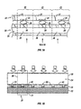
図1Aは従来技術のSBBASIC型半導体輻射線像形成素子の断面の概略側面図であり、そこでは各ピクセル回路は単一の検出器ピクセルと組み合わされており、また逆もまた同様であり、ピクセル検出器の数とピクセル回路の間の対応比1をもつ像形成素子を示す。
BRIEF DESCRIPTION OF THE DRAWINGS FIG. 1A is a schematic side view of a cross section of a prior art SBBASIC type semiconductor radiation imaging element, where each pixel circuit is combined with a single detector pixel, and vice versa. And shows an imaging element with a corresponding ratio of 1 between the number of pixel detectors and the pixel circuit.
図1Bは従来技術のSBBASIC型半導体輻射線像形成素子の断面の側面図の代替概略図である。 FIG. 1B is an alternative schematic diagram of a cross-sectional side view of a prior art SBBASIC type semiconductor radiation imaging element.
図2は従来技術のSBBASIC型半導体輻射線像形成素子の断面の側面図の概略図であり、そこでは各ピクセル回路は単一の検出器ピクセルと組み合わされているが、各検出器ピクセルは一つより多いピクセル回路と組み合わされており、ピクセル検出器の数とピクセル回路の間の対応比<1を持つ像形成素子を示す。 FIG. 2 is a schematic side view of a cross-section of a prior art SBBASIC type semiconductor radiation imaging element, where each pixel circuit is combined with a single detector pixel, each detector pixel being one Fig. 4 shows an imaging element combined with more than one pixel circuit and having a correspondence ratio <1 between the number of pixel detectors and the pixel circuit.
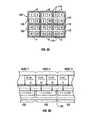
図3Aは本発明の連結検出器ピクセルセルアレイ(GDPCアレイ)のブロック概略図であり、個々の連結検出器ピクセルセルと組み合わされたピクセル検出器のそれらの内部アレイを示す。 FIG. 3A is a block schematic diagram of the coupled detector pixel cell array (GDPC array) of the present invention, showing their internal array of pixel detectors combined with individual coupled detector pixel cells.
図3Bは図3AのSBBASIC型連結検出器ピクセルセルアレイ(GDPCアレイ)の断面の概略側面図であり、単一のピクセルセル内で、各ピクセル検出器は単一のピクセル信号カウント回路と電気的に連通しているが、ピクセルセルの単一のピクセルカウント回路はセル内の検出器ピクセルの全てと電気的に連通していることを示し、単一ピクセルセル内のピクセル検出器の数とピクセル回路の間の対応比(RC)がRC=4である像形成素子を示す。
FIG. 3B is a schematic side view of a cross-section of the SBBASIC type connected detector pixel cell array (GDPC array) of FIG. 3A, wherein each pixel detector is electrically connected to a single pixel signal count circuit within a single pixel cell. Although in communication, the single pixel count circuit of the pixel cell indicates that it is in electrical communication with all of the detector pixels in the cell, and the number of pixel detectors in the single pixel cell and the
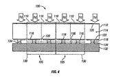
図4は本発明の連結検出器ピクセルセルのアレイの概略側面図であり、半導体基板の積層形状を示す。 FIG. 4 is a schematic side view of an array of coupled detector pixel cells of the present invention, showing a stacked configuration of semiconductor substrates.
図5は本発明のピクセル信号カウント回路の概略ブロックダイヤグラムであり、多数の(図示の場合二つの)ピクセル信号入力部と単一のパルスカウンター回路と連通しているそれらの組み合わされた信号状態調節回路を示す。 FIG. 5 is a schematic block diagram of the pixel signal counting circuit of the present invention, and their combined signal conditioning in communication with multiple (two in the illustrated case) pixel signal inputs and a single pulse counter circuit. The circuit is shown.
図6は図5と同様の本発明のピクセル信号カウント回路の概略ブロックダイヤグラムであるが、単一のパルスカウンター回路の代替実施例を示す。 FIG. 6 is a schematic block diagram of a pixel signal counting circuit of the present invention similar to FIG. 5, but showing an alternative embodiment of a single pulse counter circuit.
図7は本発明のピクセル信号カウント回路の概略ブロックダイヤグラムであり、多数の(図示の場合二つの)ピクセル信号入力と、単一のパルスカウンター回路の代替実施例と連通しているそれらの組み合わされた信号状態調節回路を示す。 FIG. 7 is a schematic block diagram of the pixel signal counting circuit of the present invention, a combination of multiple (two in the illustrated case) pixel signal inputs and their combination in communication with an alternative embodiment of a single pulse counter circuit. The signal condition adjustment circuit is shown.
図面を参照するに、本発明の好適実施例の詳細が図解的にかつ概略的に示されている。図中の同様の要素は同様の数字により示され、同様の要素は異なる小文字添字を持つ同様の数字により示される。 Referring now to the drawings, the details of a preferred embodiment of the invention are shown schematically and schematically. Like elements in the figures are indicated by like numerals, and like elements are indicated by like numerals with different lowercase suffixes.
図3Aと3Bに例示されるように、本発明のSBBASIC型X線及びガンマ線輻射エネルギー像形成素子100は複数の連結検出器ピクセルセル(GDPC)105のアレイを含む。図3AはAからFを付した6個の別個のGDPC105を持つ本発明の連結検出器ピクセルセルアレイ(GDPCアレイ)100の一例を示し、個々のGDPCはそれぞれ組み合わされた検出器ピクセル110の内部検出器アレイを持つ。もちろん実際にはGDPCアレイ100は利用可能な現在のまたは将来の半導体技術が許容するようなどのような数の個々のGDPCを含むこともできる。図3BはGDPCアレイ100の断面の概略図であり、単一のピクセルセル105内で“連結”検出器ピクセル110のそれぞれがGDPC105内の単一のピクセル信号カウント回路130と電気的に連通していることを示す。しかし、GDPC105の単一のピクセルカウント回路130はセル105内の検出器ピクセル110の全てと電気的に連通しているが、他とは連通していない。これは本発明のGDPC105が単一のGDPC105内のピクセル検出器105の数とピクセル回路の間の“対応比”(RC)1より大(>1)を持つという本発明の目的を示す。図3Aと3Bに示された例においては、対応比はRC=4である。
As illustrated in FIGS. 3A and 3B, the SBBASIC X-ray and gamma radiation
図4に例示された好適実施例において、本発明のX線及びガンマ線輻射エネルギー像形成素子は連結検出器ピクセルセル105のアレイ100を含む。各GDPC105は半導体検出器基板112上に配置された少なくとも二つの検出器ピクセル110のアレイを含む。半導体検出器基板の厚さは光導電体材料114から構成される。検出器ピクセル110のそれぞれはGDPC105の単一のピクセル信号カウント回路130と電気的に連通している。ピクセル信号カウント回路130はASIC半導体読出し基板132上に配置されている。検出器ピクセル110のピクセル電荷コレクタ電極116は光導電体材料114の付近で発生した電荷を集める。発生した電荷は検出器ピクセル110からそのピクセルコレクタ電極116を通してコレクタ電極116とピクセル回路入力134との間に配置されかつそれらと電気的に連通している電気伝導性ピクセルコンタクト118を介してピクセル回路入力134に伝導される。
In the preferred embodiment illustrated in FIG. 4, the X-ray and gamma radiation energy imaging element of the present invention includes an
半導体検出器基板112は二つの主要な表面:輻射表面120とピクセル表面122を持つ。配列された検出器ピクセル110の電荷コレクタ電極116は検出器基板112のピクセル表面122上に従来技術で既知の半導体技術を用いて加工される。検出器基板112は典型的にはその輻射表面120上に配置されたバイアス電極124を持つ。バイアス電極124は衝突輻射線に対して透明である。各電荷コレクタ電極116と組み合わせて、バイアス電極124は検出器基板112の厚さを横切ってバイアス電界を発生し、従って光導電体材料114中に発生した電荷をピクセル表面122に向けてドリフトする。コレクタ電極116は互いに間隔を置かれ及び/または絶縁されているが、ピクセル検出器110のバイアス電界はその電荷コレクタ電極116の周辺を越えて延び、従ってGDPC105にGDPC105のピクセル表面122の面積と少なくとも同じ大きさの有効電荷コレクタ表面を与える。
The
また図4に例示されるように、本発明のGDPC105はそれぞれ半導体ASIC読出し基板132を含む。多数の別個のGDPCが平坦なアレイ内に並置されているGDPCアレイ100としての本発明の好適実施例において、隣接GDPCの半導体読出し基板132(及び検出器基板112)はGDPCアレイ100全体にわたって連続している。さらに、複数の連結検出器ピクセルセルを含む大きなフォーマットのX線及びガンマ線輻射エネルギー像形成素子を構成するために多数のGDPCアレイが並置されることができる。
Further, as illustrated in FIG. 4, each
別個のGDPC105の単一のピクセル信号カウント回路130は回路アレイ内で半導体ASIC読出し基板132上に加工される。ASIC読出し基板132は検出器基板112のピクセル表面122に対向して配置された読出し表面136を持つ。GDPC105の単一のピクセル信号カウント回路130はGDPC105のASIC読出し基板132の読出し表面136上に加工された多数のピクセル信号入力部134を持つ。多数のピクセル信号入力部134はGDPC105のピクセル信号カウント回路130と電気的に連通した入力コンタクトであり、各ピクセル信号入力部134は配列された検出器ピクセル110の別個の検出器ピクセルコンタクト118と電気的に連通している。
A single pixel
さらに、図5と6に示されるように、ピクセル信号カウント回路130のピクセル信号入力部134はそれぞれピクセル信号状態調節回路140を含む。信号状態調節回路140は更に一つまたはそれより多い付随的信号状態調節/処理回路要素144を含むことができる。かかる付随的信号状態調節/処理回路要素144の例は:信号増幅回路要素、暗電流補償回路要素、パルス幅制御回路要素、利得制御回路要素、パルス形状付与回路要素、単一/多段階比較回路要素、アナログ加算回路要素、緩衝回路要素、及び当業者に既知でかつ当業者により本発明で実施可能な他の付随的回路要素を含む。
Further, as shown in FIGS. 5 and 6, the pixel
図5に例示されるように、P1及びP2の符号を付されている二つの(またはそれより多い)検出器ピクセル110はそれぞれ緩衝結合型ピクセルコンタクト118を介してそれ自身の信号状態調節回路140に伝導的に連結されている(図4参照)。各信号状態調節回路140は付随的状態調節回路要素144:例えば来入する電気信号を統合する及び/または増幅するための、増幅段階144a及び144b、を含む。ピクセル信号カウント回路130の各信号状態調節回路140の状態調節された出力148はパルスカウンター回路150と電気的に連通している。図5に示された例では、各信号状態調節回路140の状態調節された出力148はパルスカウンター回路要素150の付随的多入力比較段階144cに供給される。多入力比較段階144cは来入する信号が付随的比較段階回路要素144cからパルスカウンター160に出力されることができる前に来入するアナログ信号を出力しきい値に対してふるい分ける。
As illustrated in FIG. 5, two (or more)
電荷増幅器144aはこの分野の現在の像形成素子における全体の信号処理速度のずば抜けて最も有意な制限であることができる。各検出器ピクセル110のための信号状態調節回路140がそれぞれそれ自身の電荷増幅器A1 144aを持っており、単位像形成面積当りの検出器ピクセルの数を増やす(すなわちRC値を増やす)ことにより、GDPC105信号処理速度は実質的に増やされる。これはGDPC105を比較的高い入力ヒット率で処理させる。さらに、第一及び第二段階増幅器A1 144a及びA2 144b(及び更なる回路要素段階)は検出器暗電流補償回路要素、入力パルス幅制御回路要素、パルス形状付与回路要素、利得制御回路要素等を含むことができる。ピクセル信号カウント回路130のアナログ信号処理部をこのように二重にすることにより、本発明のGDPC105の入力輻射率及び全体の信号処理速度が増加される。
どのように本発明が達成されるかの実際例として、もし従来技術の光子/パルスカウント像形成素子の像形成面積が2cm×2cmであり、かつ検出器ピクセル寸法が0.5mm×0.5mmであるなら、そのときは、装置中に1600の画像ピクセルセルがある。本発明によれば、もしこの装置の検出器ピクセルの検出器ピクセル表面積(ピクセルの電荷コレクタ電極の面積)が少なくとも2倍に細分されるなら、これは(この例では)約0.25mm×0.5mmの寸法を持つ検出器ピクセルを、かつ2倍の数(または3200)の検出器ピクセルを生み出す。ピクセル信号カウント回路の数は1600のままである。しかし、ピクセルセルは今や本発明では二つの緩衝結合を持ち、それぞれはピクセルセルの二つの検出器ピクセルをピクセルセルの単一のピクセル信号カウント回路への二つの入力の組に連結する。結果として、従来技術の像形成素子と同じ全体の寸法を持つなら、本発明の例示像形成素子は:2倍の緩衝結合を持つが、同じ数のカウント回路を持つ。これは単なる例であり、検出器ピクセルセル寸法の分割を読出しチャネルの数を増やすことなく希望の値に対応するように選択することができることは明らかである。さらに、検出器ピクセルの小さな寸法のために、入力ノードキャパシタンスが対応して減少し、それはカウント回路の入力時により低いノイズになる。なお更に、例示の像形成素子のより大きな数の緩衝結合は類似の従来技術の像形成素子に対して半導体基板層間の機械的付着の付随的増加をもたらす。 As an actual example of how the present invention can be achieved, if the prior art photon / pulse count imaging element has an imaging area of 2 cm × 2 cm and a detector pixel size of 0.5 mm × 0.5 mm Then there are 1600 image pixel cells in the device. According to the present invention, if the detector pixel surface area of the detector pixel of the device (area of the charge collector electrode of the pixel) is subdivided at least twice, this is (in this example) about 0.25 mm × 0. Produces detector pixels with dimensions of .5 mm and twice as many (or 3200) detector pixels. The number of pixel signal count circuits remains 1600. However, the pixel cell now has two buffer couplings in the present invention, each coupling the two detector pixels of the pixel cell to two sets of inputs to the pixel cell's single pixel signal counting circuit. As a result, if it has the same overall dimensions as a prior art imaging element, the exemplary imaging element of the present invention: has twice the buffer coupling but has the same number of count circuits. This is only an example, and it is clear that the division of the detector pixel cell dimensions can be selected to correspond to the desired value without increasing the number of readout channels. Furthermore, due to the small size of the detector pixels, the input node capacitance is correspondingly reduced, which results in lower noise at the input of the count circuit. Still further, the larger number of buffer couplings in the exemplary imaging element results in a concomitant increase in mechanical adhesion between the semiconductor substrate layers relative to similar prior art imaging elements.
図6は本発明のGDPC105のパルスカウンター回路150の代替実施例を例示する。この好適実施例では、信号状態調節回路140の状態調節された信号出力148は付随的多入力アナログ加算回路要素144dと連通する。付随的多入力アナログ加算回路要素144dは二つの信号状態調節回路140の出力信号の比較回路要素144eでの処理に先立ちそれらの出力信号を一緒に加算する。このようにして、もし入力輻射ヒットが二つの検出器ピクセル110間にあり、電荷が二つの検出器ピクセルのコレクタ電極116間で共有されるなら(図4参照)、初期パルス振幅は二つの信号状態調節回路140出力信号を一緒に加算することにより回復される。
FIG. 6 illustrates an alternative embodiment of the
図7はGDPC105の別の好適実施例を例示する。二つの検出器ピクセル110(P1とP2)がそれぞれ別個のピクセル入力回路140に連結されている。各ピクセル入力回路140の状態調節されたピクセル信号出力148はそれ自身の付随的緩衝回路要素144fと連通する。緩衝出力149は付随的多段階比較回路144gと連通し、この比較回路要素144gの各段階は各段階のための異なる入力しきい値電圧Vth1,Vth2,Vth3及びVth4を持つ。同じしきい値電圧を持つ二つのピクセル入力回路140からの比較器の出力はそのときパルスカウント回路150の共通カウンター160a−dと連通する。
FIG. 7 illustrates another preferred embodiment of the
基本的に、図7はGDPC105のピクセルカウント回路130の例を示し、そこではピクセル信号状態調節回路140に加えて付随的信号状態調節/処理回路要素144及び共通多段階パルスカウンター回路要素150は一緒に二つの異なる検出器ピクセル110P1とP2に対応する単一のピクセル信号カウント回路130を構成する。
Basically, FIG. 7 shows an example of the
本発明のX線及びガンマ線輻射エネルギー像形成素子100は半導体検出器基板112上に配置された検出器ピクセルのコレクタ電極116の組み合わされた平坦面積を持つ検出器ピクセル110のアレイを含むGDPC105を持ち、この平坦面積はASIC読出し基板134上に配置された単一のピクセル信号カウント回路130の平坦面積と少なくともほぼ同じ大きさである。GDPCはピクセル信号カウント回路に対するピクセル検出器の数の対応比RC≧2を持ち、全体の輻射エネルギー像形成素子100は対応比RC>1を持つ。
The X-ray and gamma radiant
上記記載は多くの特定の事項を含むが、これらは本発明の範囲の限定として解釈されるべきではなく、むしろその一つのまたは別の好適実施例の例証として解釈されるべきである。多くの他の変更が可能であり、それらは当業者には明らかであろう。従って、本発明の範囲は添付特許請求の範囲及びそれらの均等物により決定されるべきであり、実施例だけで決定されるべきではない。 While the above description includes a number of specific items, they should not be construed as limiting the scope of the invention, but rather as an illustration of one or another preferred embodiment thereof. Many other modifications are possible and will be apparent to those skilled in the art. Accordingly, the scope of the invention should be determined by the appended claims and their equivalents, and not by example only.
Claims (13)
前記複数の連結検出器ピクセルセルの各々は、
半導体検出器基板上に配置された複数の検出器ピクセルを有する検出器ピクセルアレイと、
ASIC読出し基板上に配置された単一のピクセル信号カウント回路と
を有し、
前記ASIC読出し基板の一の面である読出し表面は、前記半導体検出器基板の一の面であるピクセル表面に対向して配置されており、
前記複数の検出器ピクセルの各々は、前記単一のピクセルセル信号カウント回路と電気的に連通している
ことを特徴とするX線及びガンマ線輻射エネルギー像形成素子。Comprising a plurality of coupled detector pixel cells ;
Each of the plurality of coupled detector pixel cells is
A detector pixel array having a plurality of detector pixels disposed on a semiconductor detector substrate;
A single pixel signal counting circuit disposed on the ASIC readout substrate;
Have
The readout surface, which is one side of the ASIC readout substrate, is disposed opposite the pixel surface, which is one side of the semiconductor detector substrate,
Each of the plurality of detector pixels is in electrical communication with the single pixel cell signal count circuit.
An X-ray and gamma-ray radiant energy imaging device characterized by the above.
前記ピクセル表面上に配置され、前記半導体検出器基板内に発生した電荷を集めるためのコレクタ電極と、
前記コレクタ電極と前記単一のピクセル信号カウント回路との間に配置され、前記集められた電荷を前記単一のピクセル信号カウント回路へ伝導するピクセルコンタクトと
を有することを特徴とする請求項1に記載のX線及びガンマ線輻射エネルギー像形成素子。 Each of the plurality of detector pixels is
A collector electrode disposed on the pixel surface for collecting the charge generated in the semiconductor detector substrate;
A pixel contact disposed between the collector electrode and the single pixel signal count circuit and conducting the collected charge to the single pixel signal count circuit;
X-ray and gamma-ray radiant energy imaging device of claim 1, characterized in that it comprises a.
前記複数のピクセル信号入力部の各々は、対応するピクセルコンタクトに電気的に連通している
ことを特徴とする請求項3に記載のX線及びガンマ線輻射エネルギー像形成素子。 Each of the plurality of detector pixels has a pixel contact that conducts charge generated in the semiconductor detector substrate to the single pixel signal counting circuit;
Each of the plurality of pixel signal inputs is in electrical communication with a corresponding pixel contact.
The X-ray and gamma-ray radiant energy imaging element according to claim 3 .
前記連結検出器ピクセルセルは、 The connected detector pixel cell is
半導体検出器基板に配置された複数の検出器ピクセルを有する検出器ピクセルアレイと、 A detector pixel array having a plurality of detector pixels disposed on a semiconductor detector substrate;
前記半導体検出器基板に対向して配置されたASIC読出し基板に配置され、前記複数の検出器ピクセルの少なくとも一部と電気的に連通されたピクセル信号カウント回路と A pixel signal count circuit disposed on an ASIC readout substrate disposed opposite the semiconductor detector substrate and in electrical communication with at least some of the plurality of detector pixels;
を有し、 Have
前記ピクセル信号カウント回路の個数は、前記複数の検出器ピクセルの個数より少ない The number of pixel signal count circuits is less than the number of the plurality of detector pixels.
ことを特徴とするX線及びガンマ線輻射エネルギー像形成素子。 An X-ray and gamma-ray radiant energy imaging device characterized by the above.
前記少なくとも4つの検出器ピクセルの各々は、前記単一のピクセル信号カウント回路と電気的に連通している Each of the at least four detector pixels is in electrical communication with the single pixel signal count circuit.
ことを特徴とする請求項1に記載のX線及びガンマ線輻射エネルギー像形成素子。 The X-ray and gamma-ray radiant energy imaging element according to claim 1.
複数の前記コレクタ電極の平坦面積の合計としての前記検出器ピクセルアレイの平坦面積は、前記単一のピクセル信号カウント回路の平坦面積と少なくとも同じである
ことを特徴とする請求項1に記載のX線及びガンマ線輻射エネルギー像形成素子。 Each of the plurality of detector pixels has a collector electrode disposed on the pixel surface;
The flat area of the detector pixel array as the sum of the flat areas of the plurality of collector electrodes is at least the flat area of the single pixel signal counting circuit.
The X-ray and gamma-ray radiant energy imaging element according to claim 1.
半導体検出器基板上に密接して配置された複数の検出器ピクセルを有する検出器ピクセルアレイと、 A detector pixel array having a plurality of detector pixels closely arranged on a semiconductor detector substrate;
前記半導体検出器基板に対向して配置されたASIC読出し基板上に配置された単一のピクセル信号カウント回路と A single pixel signal count circuit disposed on an ASIC readout substrate disposed opposite the semiconductor detector substrate;
を備え、 With
前記複数の検出器ピクセルの全ては、前記単一のピクセル信号カウント回路と電気的に連通している All of the plurality of detector pixels are in electrical communication with the single pixel signal counting circuit.
ことを特徴とする連結検出器ピクセルセル。 A connected detector pixel cell.
Applications Claiming Priority (3)
| Application Number | Priority Date | Filing Date | Title |
|---|---|---|---|
| US10/194,336 | 2002-07-11 | ||
| US10/194,336 US7361881B2 (en) | 2002-03-13 | 2002-07-11 | Ganged detector pixel, photon/pulse counting radiation imaging device |
| PCT/US2003/020839 WO2004008488A2 (en) | 2002-07-11 | 2003-07-03 | Ganged detector pixel, photon/pulse counting radiation imaging device |
Publications (2)
| Publication Number | Publication Date |
|---|---|
| JP2006506829A JP2006506829A (en) | 2006-02-23 |
| JP4780765B2 true JP4780765B2 (en) | 2011-09-28 |
Family
ID=30114714
Family Applications (1)
| Application Number | Title | Priority Date | Filing Date |
|---|---|---|---|
| JP2005512631A Expired - Fee Related JP4780765B2 (en) | 2002-07-11 | 2003-07-03 | Coupled detector pixel, photon / pulse count radiation imaging element |
Country Status (5)
| Country | Link |
|---|---|
| US (1) | US7361881B2 (en) |
| EP (1) | EP1540730B1 (en) |
| JP (1) | JP4780765B2 (en) |
| ES (1) | ES2679099T3 (en) |
| WO (1) | WO2004008488A2 (en) |
Families Citing this family (26)
| Publication number | Priority date | Publication date | Assignee | Title |
|---|---|---|---|---|
| US7361881B2 (en) * | 2002-03-13 | 2008-04-22 | Oy Ajat Ltd | Ganged detector pixel, photon/pulse counting radiation imaging device |
| US7208739B1 (en) | 2005-11-30 | 2007-04-24 | General Electric Company | Method and apparatus for correction of pileup and charge sharing in x-ray images with energy resolution |
| US7633068B2 (en) * | 2006-03-15 | 2009-12-15 | Endicott Interconnect Technologies, Inc. | Count uniformity correction in flux space for pixilated semiconducting radiation detectors |
| US8354650B2 (en) * | 2006-03-22 | 2013-01-15 | Endicott Interconnect Technologies, Inc. | Multi-window signal processing electronics architecture for photon counting with multi-element sensors |
| US7682930B2 (en) * | 2006-06-09 | 2010-03-23 | Aptina Imaging Corporation | Method of forming elevated photosensor and resulting structure |
| US20100172466A1 (en) * | 2006-08-14 | 2010-07-08 | Koninklijke Philips Electronics N. V. | Radiation detector with counting electronics |
| GB2444777B (en) * | 2006-12-13 | 2011-06-29 | Lancaster University | Detection of radiation |
| JP2011509399A (en) * | 2007-12-20 | 2011-03-24 | コーニンクレッカ フィリップス エレクトロニクス エヌ ヴィ | Direct conversion detector |
| GB2466213B (en) * | 2008-12-12 | 2013-03-06 | Cmosis Nv | Pixel array with shared readout circuitry |
| JP2012525203A (en) | 2009-04-29 | 2012-10-22 | エックスカウンター アーベー | Computed tomography scanning system |
| FI122647B (en) | 2009-06-09 | 2012-05-15 | Planmeca Oy | Digital x-ray sensor arrangement and digital x-ray imaging method |
| JP5521721B2 (en) | 2009-08-28 | 2014-06-18 | ソニー株式会社 | Image sensor and camera system |
| TWI441512B (en) | 2009-10-01 | 2014-06-11 | Sony Corp | Image taking device and camera system |
| KR101634250B1 (en) * | 2010-06-21 | 2016-06-28 | 삼성전자주식회사 | Large-scaled x-ray detector and method of manufacturing the same |
| EP2407109B1 (en) | 2010-07-14 | 2016-01-06 | XCounter AB | Computed tomography scanning system and method |
| US9310495B2 (en) | 2011-05-04 | 2016-04-12 | Oy Ajat Ltd. | Photon/energy identifying X-ray and gamma ray imaging device (“PID”) with a two dimensional array of pixels and system therefrom |
| DE102011077859B4 (en) | 2011-06-21 | 2014-01-23 | Siemens Aktiengesellschaft | Quantum counting radiation detector |
| US9036065B1 (en) * | 2012-08-16 | 2015-05-19 | Rambus Inc. | Shared-counter image sensor |
| US9261609B2 (en) | 2012-08-20 | 2016-02-16 | General Electric Company | Apparatus and methods for charge collection control in radiation detectors |
| WO2017009736A1 (en) | 2015-07-13 | 2017-01-19 | Koninklijke Philips N.V. | High energy resolution / high x-ray flux photon counting detector |
| US10007007B2 (en) * | 2015-09-08 | 2018-06-26 | Shenzhen Xpectvision Technology Co., Ltd. | Methods for making an X-ray detector |
| US10117626B2 (en) * | 2015-09-29 | 2018-11-06 | General Electric Company | Apparatus and method for pile-up correction in photon-counting detector |
| US10375168B2 (en) * | 2016-05-31 | 2019-08-06 | Veritas Technologies Llc | Throughput in openfabrics environments |
| JP6877772B2 (en) | 2016-10-27 | 2021-05-26 | 株式会社リガク | Detector |
| WO2020106199A1 (en) * | 2018-11-19 | 2020-05-28 | Prismatic Sensors Ab | Edge-on photon-counting detector |
| US20230314635A1 (en) * | 2020-09-02 | 2023-10-05 | The Research Foundation For The State University Of New York | Tapered scintillator crystal modules and methods of using the same |
Family Cites Families (37)
| Publication number | Priority date | Publication date | Assignee | Title |
|---|---|---|---|---|
| US5146406A (en) * | 1989-08-16 | 1992-09-08 | International Business Machines Corporation | Computer method for identifying predicate-argument structures in natural language text |
| US5262871A (en) * | 1989-11-13 | 1993-11-16 | Rutgers, The State University | Multiple resolution image sensor |
| JP2890553B2 (en) * | 1989-11-24 | 1999-05-17 | 株式会社島津製作所 | X-ray imaging device |
| EP0494573A1 (en) * | 1991-01-08 | 1992-07-15 | International Business Machines Corporation | Method for automatically disambiguating the synonymic links in a dictionary for a natural language processing system |
| US5377103A (en) * | 1992-05-15 | 1994-12-27 | International Business Machines Corporation | Constrained natural language interface for a computer that employs a browse function |
| US5369575A (en) * | 1992-05-15 | 1994-11-29 | International Business Machines Corporation | Constrained natural language interface for a computer system |
| US5630121A (en) * | 1993-02-02 | 1997-05-13 | International Business Machines Corporation | Archiving and retrieving multimedia objects using structured indexes |
| GB2279164A (en) * | 1993-06-18 | 1994-12-21 | Canon Res Ct Europe Ltd | Processing a bilingual database. |
| JP3408291B2 (en) * | 1993-09-20 | 2003-05-19 | 株式会社東芝 | Dictionary creation support device |
| EP0672989A3 (en) * | 1994-03-15 | 1998-10-28 | Toppan Printing Co., Ltd. | Machine translation system |
| GB2289983B (en) * | 1994-06-01 | 1996-10-16 | Simage Oy | Imaging devices,systems and methods |
| US5799268A (en) * | 1994-09-28 | 1998-08-25 | Apple Computer, Inc. | Method for extracting knowledge from online documentation and creating a glossary, index, help database or the like |
| US5665959A (en) * | 1995-01-13 | 1997-09-09 | The United States Of America As Represented By The Administrator Of The National Aeronautics And Space Adminstration | Solid-state image sensor with focal-plane digital photon-counting pixel array |
| DE19503364C2 (en) * | 1995-02-02 | 1999-08-26 | Siemens Ag | X-ray imaging system |
| GB2318411B (en) * | 1996-10-15 | 1999-03-10 | Simage Oy | Imaging device for imaging radiation |
| US6085162A (en) * | 1996-10-18 | 2000-07-04 | Gedanken Corporation | Translation system and method in which words are translated by a specialized dictionary and then a general dictionary |
| US6011531A (en) * | 1996-10-21 | 2000-01-04 | Xerox Corporation | Methods and applications of combining pixels to the gate and data lines for 2-D imaging and display arrays |
| GB2319394B (en) * | 1996-12-27 | 1998-10-28 | Simage Oy | Bump-bonded semiconductor imaging device |
| EP1060414B1 (en) * | 1997-02-18 | 2003-11-19 | Simage Oy | Semiconductor imaging device |
| US5991710A (en) * | 1997-05-20 | 1999-11-23 | International Business Machines Corporation | Statistical translation system with features based on phrases or groups of words |
| US6078878A (en) * | 1997-07-31 | 2000-06-20 | Microsoft Corporation | Bootstrapping sense characterizations of occurrences of polysemous words |
| US6107655A (en) * | 1997-08-15 | 2000-08-22 | Eastman Kodak Company | Active pixel image sensor with shared amplifier read-out |
| US6069362A (en) * | 1998-05-14 | 2000-05-30 | The University Of Akron | Multi-density and multi-atomic number detector media for applications |
| JP3114703B2 (en) * | 1998-07-02 | 2000-12-04 | 富士ゼロックス株式会社 | Bilingual sentence search device |
| US6285978B1 (en) * | 1998-09-24 | 2001-09-04 | International Business Machines Corporation | System and method for estimating accuracy of an automatic natural language translation |
| US6175611B1 (en) * | 1998-10-06 | 2001-01-16 | Cardiac Mariners, Inc. | Tiered detector assembly |
| US6181775B1 (en) * | 1998-11-25 | 2001-01-30 | Westell Technologies, Inc. | Dual test mode network interface unit for remote testing of transmission line and customer equipment |
| WO2000065376A1 (en) * | 1999-04-26 | 2000-11-02 | Simage Oy | Device for imaging radiation |
| DE19938793A1 (en) * | 1999-08-16 | 2001-04-12 | Siemens Ag | CT device with multi-line detector system |
| US6393389B1 (en) * | 1999-09-23 | 2002-05-21 | Xerox Corporation | Using ranked translation choices to obtain sequences indicating meaning of multi-token expressions |
| US6330530B1 (en) * | 1999-10-18 | 2001-12-11 | Sony Corporation | Method and system for transforming a source language linguistic structure into a target language linguistic structure based on example linguistic feature structures |
| EP1102323B1 (en) * | 1999-11-19 | 2012-08-15 | CSEM Centre Suisse d'Electronique et de Microtechnique SA - Recherche et Développement | Method for detecting electromagnetic radiation using an optoelectronic sensor |
| US7962326B2 (en) * | 2000-04-20 | 2011-06-14 | Invention Machine Corporation | Semantic answering system and method |
| WO2002043366A2 (en) * | 2000-11-27 | 2002-05-30 | Vision Sciences Inc. | Programmable resolution cmos image sensor |
| US7189971B2 (en) * | 2002-02-15 | 2007-03-13 | Oy Ajat Ltd | Radiation imaging device and system |
| US6933505B2 (en) * | 2002-03-13 | 2005-08-23 | Oy Ajat Ltd | Low temperature, bump-bonded radiation imaging device |
| US7361881B2 (en) * | 2002-03-13 | 2008-04-22 | Oy Ajat Ltd | Ganged detector pixel, photon/pulse counting radiation imaging device |
-
2002
- 2002-07-11 US US10/194,336 patent/US7361881B2/en not_active Expired - Fee Related
-
2003
- 2003-07-03 EP EP03817490.0A patent/EP1540730B1/en not_active Expired - Lifetime
- 2003-07-03 ES ES03817490.0T patent/ES2679099T3/en not_active Expired - Lifetime
- 2003-07-03 WO PCT/US2003/020839 patent/WO2004008488A2/en active Search and Examination
- 2003-07-03 JP JP2005512631A patent/JP4780765B2/en not_active Expired - Fee Related
Also Published As
| Publication number | Publication date |
|---|---|
| EP1540730A2 (en) | 2005-06-15 |
| EP1540730B1 (en) | 2018-06-13 |
| US20030173522A1 (en) | 2003-09-18 |
| WO2004008488A9 (en) | 2004-06-10 |
| ES2679099T3 (en) | 2018-08-22 |
| US7361881B2 (en) | 2008-04-22 |
| JP2006506829A (en) | 2006-02-23 |
| WO2004008488A2 (en) | 2004-01-22 |
| WO2004008488A3 (en) | 2004-09-02 |
| WO2004008488A8 (en) | 2005-02-17 |
| EP1540730A4 (en) | 2007-07-11 |
Similar Documents
| Publication | Publication Date | Title |
|---|---|---|
| JP4780765B2 (en) | Coupled detector pixel, photon / pulse count radiation imaging element | |
| US6002134A (en) | Cross-strip semiconductor detector with cord-wood construction | |
| US5693947A (en) | Radiation detectors | |
| EP0722188B1 (en) | Image capture panel using a solid state device | |
| JP4989005B2 (en) | Digital X-ray imaging method and sensor device | |
| US7064338B2 (en) | Two-dimensional radiation detector | |
| US5099128A (en) | High resolution position sensitive detector | |
| US6037595A (en) | Radiation detector with shielding electrode | |
| EP0239808B1 (en) | Radiation detecting device | |
| US5220170A (en) | X-ray imaging system and solid state detector therefor | |
| EP2005215B1 (en) | Multi-layer pixellated gamma-ray detector | |
| US5929449A (en) | Flat panel detector for radiation imaging with reduced electronic noise | |
| JPH11515093A (en) | Flat panel detector for radiation imaging with reduced trapped charge | |
| US7233003B2 (en) | Radiation detector | |
| US20050184244A1 (en) | Radiation detector and light or radiation detector | |
| US20010035497A1 (en) | Detector support device for detecting ionizing radiations | |
| US8513617B2 (en) | Edge-on two-dimensional detector arrays | |
| JPH0784055A (en) | Radiation two-dimensional detector | |
| US6080997A (en) | Electromagnetic-wave detector | |
| US6373062B1 (en) | Interdigital photodetector for indirect x-ray detection in a radiography imaging system | |
| US20160161426A1 (en) | Pillar Based Amorphous and Polycrystalline Photoconductors for X-ray Image Sensors | |
| US6586742B2 (en) | Method and arrangement relating to x-ray imaging | |
| JP2000046951A (en) | Radiation detection element | |
| JPH07107942B2 (en) | Radiation detector |
Legal Events
| Date | Code | Title | Description |
|---|---|---|---|
| A621 | Written request for application examination |
Free format text: JAPANESE INTERMEDIATE CODE: A621 Effective date: 20060605 |
|
| A977 | Report on retrieval |
Free format text: JAPANESE INTERMEDIATE CODE: A971007 Effective date: 20091007 |
|
| A131 | Notification of reasons for refusal |
Free format text: JAPANESE INTERMEDIATE CODE: A131 Effective date: 20091016 |
|
| A601 | Written request for extension of time |
Free format text: JAPANESE INTERMEDIATE CODE: A601 Effective date: 20091211 |
|
| A602 | Written permission of extension of time |
Free format text: JAPANESE INTERMEDIATE CODE: A602 Effective date: 20091218 |
|
| A521 | Request for written amendment filed |
Free format text: JAPANESE INTERMEDIATE CODE: A821 Effective date: 20100325 |
|
| RD02 | Notification of acceptance of power of attorney |
Free format text: JAPANESE INTERMEDIATE CODE: A7422 Effective date: 20100325 |
|
| A521 | Request for written amendment filed |
Free format text: JAPANESE INTERMEDIATE CODE: A523 Effective date: 20100401 |
|
| RD04 | Notification of resignation of power of attorney |
Free format text: JAPANESE INTERMEDIATE CODE: A7424 Effective date: 20100407 |
|
| A521 | Request for written amendment filed |
Free format text: JAPANESE INTERMEDIATE CODE: A821 Effective date: 20100325 |
|
| TRDD | Decision of grant or rejection written | ||
| A01 | Written decision to grant a patent or to grant a registration (utility model) |
Free format text: JAPANESE INTERMEDIATE CODE: A01 Effective date: 20110621 |
|
| A01 | Written decision to grant a patent or to grant a registration (utility model) |
Free format text: JAPANESE INTERMEDIATE CODE: A01 |
|
| A61 | First payment of annual fees (during grant procedure) |
Free format text: JAPANESE INTERMEDIATE CODE: A61 Effective date: 20110704 |
|
| FPAY | Renewal fee payment (event date is renewal date of database) |
Free format text: PAYMENT UNTIL: 20140715 Year of fee payment: 3 |
|
| R150 | Certificate of patent or registration of utility model |
Ref document number: 4780765 Country of ref document: JP Free format text: JAPANESE INTERMEDIATE CODE: R150 Free format text: JAPANESE INTERMEDIATE CODE: R150 |
|
| R250 | Receipt of annual fees |
Free format text: JAPANESE INTERMEDIATE CODE: R250 |
|
| R250 | Receipt of annual fees |
Free format text: JAPANESE INTERMEDIATE CODE: R250 |
|
| R250 | Receipt of annual fees |
Free format text: JAPANESE INTERMEDIATE CODE: R250 |
|
| R250 | Receipt of annual fees |
Free format text: JAPANESE INTERMEDIATE CODE: R250 |
|
| R250 | Receipt of annual fees |
Free format text: JAPANESE INTERMEDIATE CODE: R250 |
|
| R250 | Receipt of annual fees |
Free format text: JAPANESE INTERMEDIATE CODE: R250 |
|
| R250 | Receipt of annual fees |
Free format text: JAPANESE INTERMEDIATE CODE: R250 |
|
| R250 | Receipt of annual fees |
Free format text: JAPANESE INTERMEDIATE CODE: R250 |
|
| LAPS | Cancellation because of no payment of annual fees |