JP4776675B2 - Semiconductor memory card - Google Patents
Semiconductor memory card Download PDFInfo
- Publication number
- JP4776675B2 JP4776675B2 JP2008280713A JP2008280713A JP4776675B2 JP 4776675 B2 JP4776675 B2 JP 4776675B2 JP 2008280713 A JP2008280713 A JP 2008280713A JP 2008280713 A JP2008280713 A JP 2008280713A JP 4776675 B2 JP4776675 B2 JP 4776675B2
- Authority
- JP
- Japan
- Prior art keywords
- pad
- wiring board
- memory
- long side
- electrode
- Prior art date
- Legal status (The legal status is an assumption and is not a legal conclusion. Google has not performed a legal analysis and makes no representation as to the accuracy of the status listed.)
- Expired - Fee Related
Links
Images


Classifications
-
- H—ELECTRICITY
- H01—ELECTRIC ELEMENTS
- H01L—SEMICONDUCTOR DEVICES NOT COVERED BY CLASS H10
- H01L25/00—Assemblies consisting of a plurality of individual semiconductor or other solid state devices ; Multistep manufacturing processes thereof
- H01L25/03—Assemblies consisting of a plurality of individual semiconductor or other solid state devices ; Multistep manufacturing processes thereof all the devices being of a type provided for in the same subgroup of groups H01L27/00 - H01L33/00, or in a single subclass of H10K, H10N, e.g. assemblies of rectifier diodes
- H01L25/04—Assemblies consisting of a plurality of individual semiconductor or other solid state devices ; Multistep manufacturing processes thereof all the devices being of a type provided for in the same subgroup of groups H01L27/00 - H01L33/00, or in a single subclass of H10K, H10N, e.g. assemblies of rectifier diodes the devices not having separate containers
- H01L25/065—Assemblies consisting of a plurality of individual semiconductor or other solid state devices ; Multistep manufacturing processes thereof all the devices being of a type provided for in the same subgroup of groups H01L27/00 - H01L33/00, or in a single subclass of H10K, H10N, e.g. assemblies of rectifier diodes the devices not having separate containers the devices being of a type provided for in group H01L27/00
- H01L25/0657—Stacked arrangements of devices
-
- H—ELECTRICITY
- H01—ELECTRIC ELEMENTS
- H01L—SEMICONDUCTOR DEVICES NOT COVERED BY CLASS H10
- H01L24/00—Arrangements for connecting or disconnecting semiconductor or solid-state bodies; Methods or apparatus related thereto
- H01L24/01—Means for bonding being attached to, or being formed on, the surface to be connected, e.g. chip-to-package, die-attach, "first-level" interconnects; Manufacturing methods related thereto
- H01L24/42—Wire connectors; Manufacturing methods related thereto
- H01L24/47—Structure, shape, material or disposition of the wire connectors after the connecting process
- H01L24/49—Structure, shape, material or disposition of the wire connectors after the connecting process of a plurality of wire connectors
-
- H—ELECTRICITY
- H01—ELECTRIC ELEMENTS
- H01L—SEMICONDUCTOR DEVICES NOT COVERED BY CLASS H10
- H01L2224/00—Indexing scheme for arrangements for connecting or disconnecting semiconductor or solid-state bodies and methods related thereto as covered by H01L24/00
- H01L2224/01—Means for bonding being attached to, or being formed on, the surface to be connected, e.g. chip-to-package, die-attach, "first-level" interconnects; Manufacturing methods related thereto
- H01L2224/02—Bonding areas; Manufacturing methods related thereto
- H01L2224/04—Structure, shape, material or disposition of the bonding areas prior to the connecting process
- H01L2224/05—Structure, shape, material or disposition of the bonding areas prior to the connecting process of an individual bonding area
- H01L2224/0554—External layer
- H01L2224/0555—Shape
- H01L2224/05552—Shape in top view
- H01L2224/05554—Shape in top view being square
-
- H—ELECTRICITY
- H01—ELECTRIC ELEMENTS
- H01L—SEMICONDUCTOR DEVICES NOT COVERED BY CLASS H10
- H01L2224/00—Indexing scheme for arrangements for connecting or disconnecting semiconductor or solid-state bodies and methods related thereto as covered by H01L24/00
- H01L2224/01—Means for bonding being attached to, or being formed on, the surface to be connected, e.g. chip-to-package, die-attach, "first-level" interconnects; Manufacturing methods related thereto
- H01L2224/02—Bonding areas; Manufacturing methods related thereto
- H01L2224/04—Structure, shape, material or disposition of the bonding areas prior to the connecting process
- H01L2224/05—Structure, shape, material or disposition of the bonding areas prior to the connecting process of an individual bonding area
- H01L2224/0554—External layer
- H01L2224/05599—Material
-
- H—ELECTRICITY
- H01—ELECTRIC ELEMENTS
- H01L—SEMICONDUCTOR DEVICES NOT COVERED BY CLASS H10
- H01L2224/00—Indexing scheme for arrangements for connecting or disconnecting semiconductor or solid-state bodies and methods related thereto as covered by H01L24/00
- H01L2224/01—Means for bonding being attached to, or being formed on, the surface to be connected, e.g. chip-to-package, die-attach, "first-level" interconnects; Manufacturing methods related thereto
- H01L2224/26—Layer connectors, e.g. plate connectors, solder or adhesive layers; Manufacturing methods related thereto
- H01L2224/31—Structure, shape, material or disposition of the layer connectors after the connecting process
- H01L2224/32—Structure, shape, material or disposition of the layer connectors after the connecting process of an individual layer connector
- H01L2224/321—Disposition
- H01L2224/32135—Disposition the layer connector connecting between different semiconductor or solid-state bodies, i.e. chip-to-chip
- H01L2224/32145—Disposition the layer connector connecting between different semiconductor or solid-state bodies, i.e. chip-to-chip the bodies being stacked
-
- H—ELECTRICITY
- H01—ELECTRIC ELEMENTS
- H01L—SEMICONDUCTOR DEVICES NOT COVERED BY CLASS H10
- H01L2224/00—Indexing scheme for arrangements for connecting or disconnecting semiconductor or solid-state bodies and methods related thereto as covered by H01L24/00
- H01L2224/01—Means for bonding being attached to, or being formed on, the surface to be connected, e.g. chip-to-package, die-attach, "first-level" interconnects; Manufacturing methods related thereto
- H01L2224/26—Layer connectors, e.g. plate connectors, solder or adhesive layers; Manufacturing methods related thereto
- H01L2224/31—Structure, shape, material or disposition of the layer connectors after the connecting process
- H01L2224/32—Structure, shape, material or disposition of the layer connectors after the connecting process of an individual layer connector
- H01L2224/321—Disposition
- H01L2224/32151—Disposition the layer connector connecting between a semiconductor or solid-state body and an item not being a semiconductor or solid-state body, e.g. chip-to-substrate, chip-to-passive
- H01L2224/32221—Disposition the layer connector connecting between a semiconductor or solid-state body and an item not being a semiconductor or solid-state body, e.g. chip-to-substrate, chip-to-passive the body and the item being stacked
- H01L2224/32225—Disposition the layer connector connecting between a semiconductor or solid-state body and an item not being a semiconductor or solid-state body, e.g. chip-to-substrate, chip-to-passive the body and the item being stacked the item being non-metallic, e.g. insulating substrate with or without metallisation
-
- H—ELECTRICITY
- H01—ELECTRIC ELEMENTS
- H01L—SEMICONDUCTOR DEVICES NOT COVERED BY CLASS H10
- H01L2224/00—Indexing scheme for arrangements for connecting or disconnecting semiconductor or solid-state bodies and methods related thereto as covered by H01L24/00
- H01L2224/01—Means for bonding being attached to, or being formed on, the surface to be connected, e.g. chip-to-package, die-attach, "first-level" interconnects; Manufacturing methods related thereto
- H01L2224/42—Wire connectors; Manufacturing methods related thereto
- H01L2224/44—Structure, shape, material or disposition of the wire connectors prior to the connecting process
- H01L2224/45—Structure, shape, material or disposition of the wire connectors prior to the connecting process of an individual wire connector
- H01L2224/45001—Core members of the connector
- H01L2224/45099—Material
- H01L2224/451—Material with a principal constituent of the material being a metal or a metalloid, e.g. boron (B), silicon (Si), germanium (Ge), arsenic (As), antimony (Sb), tellurium (Te) and polonium (Po), and alloys thereof
- H01L2224/45138—Material with a principal constituent of the material being a metal or a metalloid, e.g. boron (B), silicon (Si), germanium (Ge), arsenic (As), antimony (Sb), tellurium (Te) and polonium (Po), and alloys thereof the principal constituent melting at a temperature of greater than or equal to 950°C and less than 1550°C
- H01L2224/45144—Gold (Au) as principal constituent
-
- H—ELECTRICITY
- H01—ELECTRIC ELEMENTS
- H01L—SEMICONDUCTOR DEVICES NOT COVERED BY CLASS H10
- H01L2224/00—Indexing scheme for arrangements for connecting or disconnecting semiconductor or solid-state bodies and methods related thereto as covered by H01L24/00
- H01L2224/01—Means for bonding being attached to, or being formed on, the surface to be connected, e.g. chip-to-package, die-attach, "first-level" interconnects; Manufacturing methods related thereto
- H01L2224/42—Wire connectors; Manufacturing methods related thereto
- H01L2224/44—Structure, shape, material or disposition of the wire connectors prior to the connecting process
- H01L2224/45—Structure, shape, material or disposition of the wire connectors prior to the connecting process of an individual wire connector
- H01L2224/45001—Core members of the connector
- H01L2224/45099—Material
- H01L2224/451—Material with a principal constituent of the material being a metal or a metalloid, e.g. boron (B), silicon (Si), germanium (Ge), arsenic (As), antimony (Sb), tellurium (Te) and polonium (Po), and alloys thereof
- H01L2224/45138—Material with a principal constituent of the material being a metal or a metalloid, e.g. boron (B), silicon (Si), germanium (Ge), arsenic (As), antimony (Sb), tellurium (Te) and polonium (Po), and alloys thereof the principal constituent melting at a temperature of greater than or equal to 950°C and less than 1550°C
- H01L2224/45147—Copper (Cu) as principal constituent
-
- H—ELECTRICITY
- H01—ELECTRIC ELEMENTS
- H01L—SEMICONDUCTOR DEVICES NOT COVERED BY CLASS H10
- H01L2224/00—Indexing scheme for arrangements for connecting or disconnecting semiconductor or solid-state bodies and methods related thereto as covered by H01L24/00
- H01L2224/01—Means for bonding being attached to, or being formed on, the surface to be connected, e.g. chip-to-package, die-attach, "first-level" interconnects; Manufacturing methods related thereto
- H01L2224/42—Wire connectors; Manufacturing methods related thereto
- H01L2224/47—Structure, shape, material or disposition of the wire connectors after the connecting process
- H01L2224/48—Structure, shape, material or disposition of the wire connectors after the connecting process of an individual wire connector
- H01L2224/4805—Shape
- H01L2224/4809—Loop shape
- H01L2224/48091—Arched
-
- H—ELECTRICITY
- H01—ELECTRIC ELEMENTS
- H01L—SEMICONDUCTOR DEVICES NOT COVERED BY CLASS H10
- H01L2224/00—Indexing scheme for arrangements for connecting or disconnecting semiconductor or solid-state bodies and methods related thereto as covered by H01L24/00
- H01L2224/01—Means for bonding being attached to, or being formed on, the surface to be connected, e.g. chip-to-package, die-attach, "first-level" interconnects; Manufacturing methods related thereto
- H01L2224/42—Wire connectors; Manufacturing methods related thereto
- H01L2224/47—Structure, shape, material or disposition of the wire connectors after the connecting process
- H01L2224/48—Structure, shape, material or disposition of the wire connectors after the connecting process of an individual wire connector
- H01L2224/481—Disposition
- H01L2224/48135—Connecting between different semiconductor or solid-state bodies, i.e. chip-to-chip
- H01L2224/48145—Connecting between different semiconductor or solid-state bodies, i.e. chip-to-chip the bodies being stacked
- H01L2224/48147—Connecting between different semiconductor or solid-state bodies, i.e. chip-to-chip the bodies being stacked with an intermediate bond, e.g. continuous wire daisy chain
-
- H—ELECTRICITY
- H01—ELECTRIC ELEMENTS
- H01L—SEMICONDUCTOR DEVICES NOT COVERED BY CLASS H10
- H01L2224/00—Indexing scheme for arrangements for connecting or disconnecting semiconductor or solid-state bodies and methods related thereto as covered by H01L24/00
- H01L2224/01—Means for bonding being attached to, or being formed on, the surface to be connected, e.g. chip-to-package, die-attach, "first-level" interconnects; Manufacturing methods related thereto
- H01L2224/42—Wire connectors; Manufacturing methods related thereto
- H01L2224/47—Structure, shape, material or disposition of the wire connectors after the connecting process
- H01L2224/48—Structure, shape, material or disposition of the wire connectors after the connecting process of an individual wire connector
- H01L2224/481—Disposition
- H01L2224/48151—Connecting between a semiconductor or solid-state body and an item not being a semiconductor or solid-state body, e.g. chip-to-substrate, chip-to-passive
- H01L2224/48221—Connecting between a semiconductor or solid-state body and an item not being a semiconductor or solid-state body, e.g. chip-to-substrate, chip-to-passive the body and the item being stacked
- H01L2224/48225—Connecting between a semiconductor or solid-state body and an item not being a semiconductor or solid-state body, e.g. chip-to-substrate, chip-to-passive the body and the item being stacked the item being non-metallic, e.g. insulating substrate with or without metallisation
- H01L2224/48227—Connecting between a semiconductor or solid-state body and an item not being a semiconductor or solid-state body, e.g. chip-to-substrate, chip-to-passive the body and the item being stacked the item being non-metallic, e.g. insulating substrate with or without metallisation connecting the wire to a bond pad of the item
-
- H—ELECTRICITY
- H01—ELECTRIC ELEMENTS
- H01L—SEMICONDUCTOR DEVICES NOT COVERED BY CLASS H10
- H01L2224/00—Indexing scheme for arrangements for connecting or disconnecting semiconductor or solid-state bodies and methods related thereto as covered by H01L24/00
- H01L2224/01—Means for bonding being attached to, or being formed on, the surface to be connected, e.g. chip-to-package, die-attach, "first-level" interconnects; Manufacturing methods related thereto
- H01L2224/42—Wire connectors; Manufacturing methods related thereto
- H01L2224/47—Structure, shape, material or disposition of the wire connectors after the connecting process
- H01L2224/49—Structure, shape, material or disposition of the wire connectors after the connecting process of a plurality of wire connectors
- H01L2224/491—Disposition
- H01L2224/4912—Layout
- H01L2224/49171—Fan-out arrangements
-
- H—ELECTRICITY
- H01—ELECTRIC ELEMENTS
- H01L—SEMICONDUCTOR DEVICES NOT COVERED BY CLASS H10
- H01L2224/00—Indexing scheme for arrangements for connecting or disconnecting semiconductor or solid-state bodies and methods related thereto as covered by H01L24/00
- H01L2224/01—Means for bonding being attached to, or being formed on, the surface to be connected, e.g. chip-to-package, die-attach, "first-level" interconnects; Manufacturing methods related thereto
- H01L2224/42—Wire connectors; Manufacturing methods related thereto
- H01L2224/47—Structure, shape, material or disposition of the wire connectors after the connecting process
- H01L2224/49—Structure, shape, material or disposition of the wire connectors after the connecting process of a plurality of wire connectors
- H01L2224/491—Disposition
- H01L2224/4912—Layout
- H01L2224/49175—Parallel arrangements
-
- H—ELECTRICITY
- H01—ELECTRIC ELEMENTS
- H01L—SEMICONDUCTOR DEVICES NOT COVERED BY CLASS H10
- H01L2224/00—Indexing scheme for arrangements for connecting or disconnecting semiconductor or solid-state bodies and methods related thereto as covered by H01L24/00
- H01L2224/73—Means for bonding being of different types provided for in two or more of groups H01L2224/10, H01L2224/18, H01L2224/26, H01L2224/34, H01L2224/42, H01L2224/50, H01L2224/63, H01L2224/71
- H01L2224/732—Location after the connecting process
- H01L2224/73251—Location after the connecting process on different surfaces
- H01L2224/73265—Layer and wire connectors
-
- H—ELECTRICITY
- H01—ELECTRIC ELEMENTS
- H01L—SEMICONDUCTOR DEVICES NOT COVERED BY CLASS H10
- H01L2224/00—Indexing scheme for arrangements for connecting or disconnecting semiconductor or solid-state bodies and methods related thereto as covered by H01L24/00
- H01L2224/80—Methods for connecting semiconductor or other solid state bodies using means for bonding being attached to, or being formed on, the surface to be connected
- H01L2224/85—Methods for connecting semiconductor or other solid state bodies using means for bonding being attached to, or being formed on, the surface to be connected using a wire connector
- H01L2224/8538—Bonding interfaces outside the semiconductor or solid-state body
- H01L2224/85399—Material
-
- H—ELECTRICITY
- H01—ELECTRIC ELEMENTS
- H01L—SEMICONDUCTOR DEVICES NOT COVERED BY CLASS H10
- H01L2225/00—Details relating to assemblies covered by the group H01L25/00 but not provided for in its subgroups
- H01L2225/03—All the devices being of a type provided for in the same subgroup of groups H01L27/00 - H01L33/648 and H10K99/00
- H01L2225/04—All the devices being of a type provided for in the same subgroup of groups H01L27/00 - H01L33/648 and H10K99/00 the devices not having separate containers
- H01L2225/065—All the devices being of a type provided for in the same subgroup of groups H01L27/00 - H01L33/648 and H10K99/00 the devices not having separate containers the devices being of a type provided for in group H01L27/00
- H01L2225/06503—Stacked arrangements of devices
- H01L2225/06506—Wire or wire-like electrical connections between devices
-
- H—ELECTRICITY
- H01—ELECTRIC ELEMENTS
- H01L—SEMICONDUCTOR DEVICES NOT COVERED BY CLASS H10
- H01L2225/00—Details relating to assemblies covered by the group H01L25/00 but not provided for in its subgroups
- H01L2225/03—All the devices being of a type provided for in the same subgroup of groups H01L27/00 - H01L33/648 and H10K99/00
- H01L2225/04—All the devices being of a type provided for in the same subgroup of groups H01L27/00 - H01L33/648 and H10K99/00 the devices not having separate containers
- H01L2225/065—All the devices being of a type provided for in the same subgroup of groups H01L27/00 - H01L33/648 and H10K99/00 the devices not having separate containers the devices being of a type provided for in group H01L27/00
- H01L2225/06503—Stacked arrangements of devices
- H01L2225/0651—Wire or wire-like electrical connections from device to substrate
-
- H—ELECTRICITY
- H01—ELECTRIC ELEMENTS
- H01L—SEMICONDUCTOR DEVICES NOT COVERED BY CLASS H10
- H01L2225/00—Details relating to assemblies covered by the group H01L25/00 but not provided for in its subgroups
- H01L2225/03—All the devices being of a type provided for in the same subgroup of groups H01L27/00 - H01L33/648 and H10K99/00
- H01L2225/04—All the devices being of a type provided for in the same subgroup of groups H01L27/00 - H01L33/648 and H10K99/00 the devices not having separate containers
- H01L2225/065—All the devices being of a type provided for in the same subgroup of groups H01L27/00 - H01L33/648 and H10K99/00 the devices not having separate containers the devices being of a type provided for in group H01L27/00
- H01L2225/06503—Stacked arrangements of devices
- H01L2225/06555—Geometry of the stack, e.g. form of the devices, geometry to facilitate stacking
- H01L2225/06562—Geometry of the stack, e.g. form of the devices, geometry to facilitate stacking at least one device in the stack being rotated or offset
-
- H—ELECTRICITY
- H01—ELECTRIC ELEMENTS
- H01L—SEMICONDUCTOR DEVICES NOT COVERED BY CLASS H10
- H01L24/00—Arrangements for connecting or disconnecting semiconductor or solid-state bodies; Methods or apparatus related thereto
- H01L24/01—Means for bonding being attached to, or being formed on, the surface to be connected, e.g. chip-to-package, die-attach, "first-level" interconnects; Manufacturing methods related thereto
- H01L24/42—Wire connectors; Manufacturing methods related thereto
- H01L24/44—Structure, shape, material or disposition of the wire connectors prior to the connecting process
- H01L24/45—Structure, shape, material or disposition of the wire connectors prior to the connecting process of an individual wire connector
-
- H—ELECTRICITY
- H01—ELECTRIC ELEMENTS
- H01L—SEMICONDUCTOR DEVICES NOT COVERED BY CLASS H10
- H01L24/00—Arrangements for connecting or disconnecting semiconductor or solid-state bodies; Methods or apparatus related thereto
- H01L24/01—Means for bonding being attached to, or being formed on, the surface to be connected, e.g. chip-to-package, die-attach, "first-level" interconnects; Manufacturing methods related thereto
- H01L24/42—Wire connectors; Manufacturing methods related thereto
- H01L24/47—Structure, shape, material or disposition of the wire connectors after the connecting process
- H01L24/48—Structure, shape, material or disposition of the wire connectors after the connecting process of an individual wire connector
-
- H—ELECTRICITY
- H01—ELECTRIC ELEMENTS
- H01L—SEMICONDUCTOR DEVICES NOT COVERED BY CLASS H10
- H01L24/00—Arrangements for connecting or disconnecting semiconductor or solid-state bodies; Methods or apparatus related thereto
- H01L24/73—Means for bonding being of different types provided for in two or more of groups H01L24/10, H01L24/18, H01L24/26, H01L24/34, H01L24/42, H01L24/50, H01L24/63, H01L24/71
-
- H—ELECTRICITY
- H01—ELECTRIC ELEMENTS
- H01L—SEMICONDUCTOR DEVICES NOT COVERED BY CLASS H10
- H01L2924/00—Indexing scheme for arrangements or methods for connecting or disconnecting semiconductor or solid-state bodies as covered by H01L24/00
- H01L2924/0001—Technical content checked by a classifier
- H01L2924/00014—Technical content checked by a classifier the subject-matter covered by the group, the symbol of which is combined with the symbol of this group, being disclosed without further technical details
-
- H—ELECTRICITY
- H01—ELECTRIC ELEMENTS
- H01L—SEMICONDUCTOR DEVICES NOT COVERED BY CLASS H10
- H01L2924/00—Indexing scheme for arrangements or methods for connecting or disconnecting semiconductor or solid-state bodies as covered by H01L24/00
- H01L2924/01—Chemical elements
- H01L2924/01005—Boron [B]
-
- H—ELECTRICITY
- H01—ELECTRIC ELEMENTS
- H01L—SEMICONDUCTOR DEVICES NOT COVERED BY CLASS H10
- H01L2924/00—Indexing scheme for arrangements or methods for connecting or disconnecting semiconductor or solid-state bodies as covered by H01L24/00
- H01L2924/01—Chemical elements
- H01L2924/01006—Carbon [C]
-
- H—ELECTRICITY
- H01—ELECTRIC ELEMENTS
- H01L—SEMICONDUCTOR DEVICES NOT COVERED BY CLASS H10
- H01L2924/00—Indexing scheme for arrangements or methods for connecting or disconnecting semiconductor or solid-state bodies as covered by H01L24/00
- H01L2924/01—Chemical elements
- H01L2924/01029—Copper [Cu]
-
- H—ELECTRICITY
- H01—ELECTRIC ELEMENTS
- H01L—SEMICONDUCTOR DEVICES NOT COVERED BY CLASS H10
- H01L2924/00—Indexing scheme for arrangements or methods for connecting or disconnecting semiconductor or solid-state bodies as covered by H01L24/00
- H01L2924/01—Chemical elements
- H01L2924/01033—Arsenic [As]
-
- H—ELECTRICITY
- H01—ELECTRIC ELEMENTS
- H01L—SEMICONDUCTOR DEVICES NOT COVERED BY CLASS H10
- H01L2924/00—Indexing scheme for arrangements or methods for connecting or disconnecting semiconductor or solid-state bodies as covered by H01L24/00
- H01L2924/01—Chemical elements
- H01L2924/01078—Platinum [Pt]
-
- H—ELECTRICITY
- H01—ELECTRIC ELEMENTS
- H01L—SEMICONDUCTOR DEVICES NOT COVERED BY CLASS H10
- H01L2924/00—Indexing scheme for arrangements or methods for connecting or disconnecting semiconductor or solid-state bodies as covered by H01L24/00
- H01L2924/01—Chemical elements
- H01L2924/01079—Gold [Au]
-
- H—ELECTRICITY
- H01—ELECTRIC ELEMENTS
- H01L—SEMICONDUCTOR DEVICES NOT COVERED BY CLASS H10
- H01L2924/00—Indexing scheme for arrangements or methods for connecting or disconnecting semiconductor or solid-state bodies as covered by H01L24/00
- H01L2924/01—Chemical elements
- H01L2924/01082—Lead [Pb]
-
- H—ELECTRICITY
- H01—ELECTRIC ELEMENTS
- H01L—SEMICONDUCTOR DEVICES NOT COVERED BY CLASS H10
- H01L2924/00—Indexing scheme for arrangements or methods for connecting or disconnecting semiconductor or solid-state bodies as covered by H01L24/00
- H01L2924/013—Alloys
- H01L2924/014—Solder alloys
-
- H—ELECTRICITY
- H01—ELECTRIC ELEMENTS
- H01L—SEMICONDUCTOR DEVICES NOT COVERED BY CLASS H10
- H01L2924/00—Indexing scheme for arrangements or methods for connecting or disconnecting semiconductor or solid-state bodies as covered by H01L24/00
- H01L2924/06—Polymers
- H01L2924/078—Adhesive characteristics other than chemical
- H01L2924/07802—Adhesive characteristics other than chemical not being an ohmic electrical conductor
-
- H—ELECTRICITY
- H01—ELECTRIC ELEMENTS
- H01L—SEMICONDUCTOR DEVICES NOT COVERED BY CLASS H10
- H01L2924/00—Indexing scheme for arrangements or methods for connecting or disconnecting semiconductor or solid-state bodies as covered by H01L24/00
- H01L2924/15—Details of package parts other than the semiconductor or other solid state devices to be connected
- H01L2924/181—Encapsulation
-
- H—ELECTRICITY
- H01—ELECTRIC ELEMENTS
- H01L—SEMICONDUCTOR DEVICES NOT COVERED BY CLASS H10
- H01L2924/00—Indexing scheme for arrangements or methods for connecting or disconnecting semiconductor or solid-state bodies as covered by H01L24/00
- H01L2924/19—Details of hybrid assemblies other than the semiconductor or other solid state devices to be connected
- H01L2924/1901—Structure
- H01L2924/1904—Component type
- H01L2924/19041—Component type being a capacitor
-
- H—ELECTRICITY
- H10—SEMICONDUCTOR DEVICES; ELECTRIC SOLID-STATE DEVICES NOT OTHERWISE PROVIDED FOR
- H10B—ELECTRONIC MEMORY DEVICES
- H10B69/00—Erasable-and-programmable ROM [EPROM] devices not provided for in groups H10B41/00 - H10B63/00, e.g. ultraviolet erasable-and-programmable ROM [UVEPROM] devices
Abstract
Description
本発明は半導体メモリカードに関する。 The present invention relates to a semiconductor memory card.
NAND型フラッシュメモリ等を内蔵するメモリカード(半導体メモリカード)は、急速に小型化と高容量化が進められている。小型化されたメモリカードを実現するために、メモリ素子やコントローラ素子等の半導体素子は配線基板上に積層して搭載されている。さらに、メモリ素子自体も配線基板上に多段に積層される場合が多くなってきている。半導体素子の電極パッドはワイヤボンディングを適用し、金属ワイヤ(ボンディングワイヤ)を介して配線基板の接続パッドと電気的に接続される。 A memory card (semiconductor memory card) incorporating a NAND flash memory or the like has been rapidly reduced in size and capacity. In order to realize a miniaturized memory card, semiconductor elements such as a memory element and a controller element are stacked and mounted on a wiring board. In addition, memory elements themselves are often stacked in multiple stages on a wiring board. The electrode pads of the semiconductor element are applied with wire bonding and are electrically connected to the connection pads of the wiring board through metal wires (bonding wires).
メモリカードの高容量化を実現する上で、メモリ素子やコントローラ素子等の半導体素子の配線基板上における積層構造(搭載構造)の改良に加えて、メモリ素子自体の高密度化とそれに基づく高容量化が進められている。また、メモリ素子の外形形状は高容量化を図る上で大形化する傾向にある。ここで、メモリカードはSDTM規格等で外形寸法が規定されている。さらに、メモリカードの外周にはカードスロットに装着する際のカードの前後や表裏の向きを示す切り欠き部等が設けられている(特許文献1参照)。 In order to increase the capacity of memory cards, in addition to improving the stacked structure (mounting structure) of semiconductor elements such as memory elements and controller elements on the wiring board, the memory elements themselves have a higher density and higher capacity based on them. Is being promoted. Further, the outer shape of the memory element tends to increase in size in order to increase the capacity. Here, the outer dimensions of the memory card are defined by the SD TM standard or the like. Furthermore, the outer periphery of the memory card is provided with notches or the like indicating the front and back of the card and the direction of the front and back when the card is inserted into the card slot (see Patent Document 1).
メモリカード用の配線基板上に大形化されたメモリ素子を搭載する場合、配線基板とメモリ素子との接続が困難になるおそれがある。これは配線基板上に搭載可能なメモリ素子の数やサイズを制約する要因となる。例えば、複数のメモリ素子(半導体素子)に対してワイヤボンディングを実施するためには、短辺側に設けられた電極パッドを露出させるように、複数のメモリ素子を階段状に積層することが考えられる(特許文献2参照)。 When mounting a large-sized memory element on a wiring board for a memory card, it may be difficult to connect the wiring board and the memory element. This becomes a factor that restricts the number and size of memory elements that can be mounted on the wiring board. For example, in order to perform wire bonding on a plurality of memory elements (semiconductor elements), it is considered that a plurality of memory elements are stacked stepwise so as to expose an electrode pad provided on the short side. (See Patent Document 2).
短辺側に電極パッドを設けたメモリ素子を階段状に積層した場合、メモリ素子の積層数が増加するにつれて階段方向の長さが長くなり、配線基板に対する素子占有面積が増加する。これは配線基板に搭載可能なメモリ素子数を制約する要因となり、メモリカードに求められている高容量化を妨げる結果となる。さらに、短辺片側パッド構造を有するメモリ素子では高密度化や高機能化等に基づく電極数の増加に対応できないおそれがある。
本発明の目的は、配線基板とメモリ素子との接続を確保した上で、配線基板に搭載するメモリ素子の電極数の増加、素子形状の大型化、素子搭載数の増加等への対応を図った半導体メモリカードを提供することにある。 The object of the present invention is to secure the connection between the wiring board and the memory element and to cope with an increase in the number of electrodes of the memory element mounted on the wiring board, an increase in the element shape, an increase in the number of elements mounted, and the like. Another object is to provide a semiconductor memory card.
本発明の態様に係る半導体メモリカードは、略矩形状の外形形状と、外部接続端子を備える第1の面と、素子搭載部と少なくとも第1の長辺に沿った第1のパッド領域および第2の長辺に沿った第2のパッド領域に配置された接続パッドとを備える第2の面とを有する配線基板と;長辺に沿って配列された電極パッドを有する複数の第1のメモリ素子を備え、前記複数の第1のメモリ素子は前記長辺が前記配線基板の前記第1のパッド領域の近傍に位置すると共に前記電極パッドが露出するように、前記配線基板の前記素子搭載部上に階段状に積層されている第1の素子群と;長辺に沿って配列された電極パッドを有する複数の第2のメモリ素子を備え、前記複数の第2のメモリ素子は前記長辺が前記配線基板の前記第2のパッド領域の近傍に位置すると共に前記電極パッドが露出するように、前記第1の素子群上に前記第1の素子群の階段方向とは逆方向に向けて階段状に積層されている第2の素子群と;前記第2の素子群上に配置され、少なくとも一つの外形辺に沿って配列された電極パッドを有するコントローラ素子と;前記第1のパッド領域に配置された前記接続パッドと前記複数の第1のメモリ素子の前記電極パッドとを電気的に接続する第1の金属ワイヤと;前記第2のパッド領域に配置された前記接続パッドと前記複数の第2のメモリ素子の前記電極パッドとを電気的に接続する第2の金属ワイヤと;前記配線基板の前記接続パッドと前記コントローラ素子の前記電極パッドとを電気的に接続する第3の金属ワイヤと;前記第1および第2の素子群と前記コントローラ素子とを前記第1ないし第3の金属ワイヤと共に封止するように、前記配線基板の前記第2の面上に形成された封止樹脂層とを具備することを特徴としている。 A semiconductor memory card according to an aspect of the present invention includes a substantially rectangular outer shape, a first surface including an external connection terminal, an element mounting portion, a first pad region at least along the first long side, and a first surface. A wiring board having a second surface including a connection pad arranged in a second pad region along the two long sides; and a plurality of first memories having electrode pads arranged along the long side An element mounting portion of the wiring board, wherein the plurality of first memory elements have the long sides positioned in the vicinity of the first pad region of the wiring board and the electrode pads are exposed. A plurality of second memory elements each having an electrode pad arranged along a long side, wherein the plurality of second memory elements include the long side Is in the vicinity of the second pad region of the wiring board A second element group stacked in a staircase pattern on the first element group in a direction opposite to the staircase direction of the first element group so that the electrode pad is exposed while being positioned; A controller element having an electrode pad disposed on the second element group and arranged along at least one outer side; the connection pad disposed in the first pad region; and the plurality of first elements A first metal wire for electrically connecting the electrode pads of the memory element; and an electrical connection between the connection pads disposed in the second pad region and the electrode pads of the plurality of second memory elements. A second metal wire connected to the wiring board; a third metal wire electrically connecting the connection pad of the wiring board and the electrode pad of the controller element; the first and second element groups; control The element so as to seal with said first to third metal wires, it is characterized by comprising a sealing resin layer formed on the second surface of the wiring board.
本発明の態様に係る半導体メモリカードによれば、配線基板と電極数が多いメモリ素子との接続を確保した上で、配線基板に大形のメモリ素子を多段に搭載することが可能となる。従って、小型で高容量の半導体メモリカードを提供することができる。 According to the semiconductor memory card according to the aspect of the present invention, it is possible to mount a large number of memory elements on the wiring board in multiple stages while ensuring the connection between the wiring board and the memory element having a large number of electrodes. Therefore, a small and high capacity semiconductor memory card can be provided.
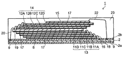
以下、本発明を実施するための形態について、図面を参照して説明する。図1および図2は本発明の第1の実施形態による半導体メモリカードを示す図である。図1は半導体メモリカードの平面図、図2は図1のA−A線に沿った断面図(メモリカードを短辺方向に切断した断面図)である。これらの図に示される半導体メモリカード1は、例えばマイクロSDTM規格のメモリカードとして使用されるものである。 Hereinafter, embodiments for carrying out the present invention will be described with reference to the drawings. 1 and 2 are views showing a semiconductor memory card according to a first embodiment of the present invention. FIG. 1 is a plan view of a semiconductor memory card, and FIG. 2 is a cross-sectional view taken along the line AA in FIG. 1 (cross-sectional view of the memory card cut in the short side direction). The semiconductor memory card 1 shown in these figures is used as, for example, a micro SD ™ standard memory card.
メモリカード1は素子搭載基板と端子形成基板とを兼ねる配線基板2を備えている。配線基板2は、例えば絶縁性樹脂基板の内部や表面に配線網を設けたものであり、具体的にはガラス−エポキシ樹脂やBT樹脂(ビスマレイミド・トリアジン樹脂)等を使用したプリント配線板が適用される。配線基板2は、端子形成面となる第1の面2aと、素子搭載面となる第2の面2bとを備えている。配線基板2の第2の面2bには、チップコンデンサやヒューズ等のチップ部品3が実装されている。
The memory card 1 includes a
配線基板2は概略矩形状の外形を有している。配線基板2の外形を構成する辺のうち、第1の短辺4Aはメモリカード1をカードスロットに挿入する際の先端部に相当する。第2の短辺4Bはメモリカード1の後方部に相当する。配線基板2の第1の長辺5Aには、メモリカード1の前後や表裏の向きを示すように、切り欠き部6やくびれ部7が設けられている。切り欠き部6は第1の短辺4Aの幅が第2の短辺4Bの幅より狭くなるように、第1の短辺4Aと第1の長辺5Aとの角部から第1の長辺5Aに沿って設けられている。
The
配線基板2は第1の長辺5Aと第1の短辺4Aとの角部(仮想角部)を含む第1の長辺5Aの一部を切り欠いた切り欠き部6を有している。切り欠き部6の端部6aは角度が鈍角となるように傾斜されている。配線基板2は第1の長辺5Aの一部を略台形状にくびれさせたくびれ部7を有している。配線基板2の各角部はR形状とされている。チップ部品3は配線基板2の両短辺4A、4B側に配置されている。切り欠き部6の形状は特に限定されるものではなく、第1の長辺5Aの一部を切り欠くものであればよい。
The
配線基板2の概略矩形状の外形形状は、第1の長辺5Aに設けられた切り欠き部6やくびれ部7によって左右非対称とされている。従って、後述するように矩形状のメモリ素子の搭載に有効な領域は、切り欠き部6から連続する部分(切り欠き部6の形成に伴う残余の長辺5Aに平行な部分)を除く第2の長辺5Bに平行な矩形領域となる。配線基板2の短辺4A、4B側については、チップ部品3の実装領域を除く領域となる。
The substantially rectangular outer shape of the
配線基板2の第1の面2aには、メモリカード1の入出力端子となる外部接続端子(図示せず)が形成されている。外部接続端子は電解めっき等により形成された金属層で構成される。配線基板2の第1の面2aはメモリカード1の表面に相当する。配線基板2の第1の面2aには、外部接続端子の形成領域を除く領域に第1の配線網(図示せず)が設けられている。第1の配線網はメモリカード1のテストパッド等を有している。第1の配線網は絶縁性の接着シールや接着テープ等を用いた絶縁層(図示せず)で覆われている。
On the
配線基板2の第2の面2bは、素子搭載部8と接続パッド9を含む第2の配線網とを備えている。配線基板2の第2の面2bはメモリカード1の裏面に対応するものである。素子搭載部8は上記したように第2の長辺5Bに平行で、かつチップ部品3の実装領域を除いた矩形領域に設けられており、これにより素子搭載面積の拡大を図ることができる。接続パッド9を有する第2の配線網は、配線基板2の図示を省略した内部配線(スルーホール等)を介して、外部接続端子や第1の配線網と電気的に接続されている。
The
接続パッド9は第1の長辺5Aに沿った第1のパッド領域10Aと第2の長辺5Bに沿った第2のパッド領域10Bと第1の短辺4Aに沿った第3のパッド領域10Cと第2の短辺4Bに沿った第4のパッド領域10Dのそれぞれに配置されている。第1のパッド領域10Aは切り欠き部6が設けられた第1の長辺5Aの残余の部分に平行な矩形領域に設定されている。接続パッド9は第1の長辺5Aの残余の部分に沿って配置されている。第2のパッド領域10Aは第2の長辺5Bに平行な領域に設定されている。
The
配線基板2の素子搭載部8には、複数のメモリ素子11、12が積層されて搭載されている。メモリ素子11は第1の素子群13を構成し、メモリ素子12は第1の素子群14を構成する。メモリ素子11、12としては、NAND型フラッシュメモリのような半導体メモリ素子が用いられる。メモリ素子12上にはコントローラ素子15が配置されている。コントローラ素子15は、複数のメモリ素子11、12からデータの書き込みや読み出しを行う素子を選択し、選択したメモリ素子11、12へのデータの書き込み、また選択したメモリ素子11、12に記憶されたデータの読み出し等を行う半導体素子である。
A plurality of memory elements 11 and 12 are stacked and mounted on the
配線基板2の第2の面2b上には、第1の素子群(メモリ素子群)13を構成する第1のメモリ素子11A、第2のメモリ素子11B、第3のメモリ素子11Cおよび第4のメモリ素子11Dが順に積層されている。第1ないし第4のメモリ素子11A〜11Dは矩形状の同一形状を有し、それぞれ電極パッド16を備えている。電極パッド16は配線基板2の第1の長辺5Aの近傍に位置する長辺11a側に配置されている。ただし、第1のパッド領域10Aは切り欠き部6を除く第1の長辺5Aの残余の部分に設けられているため、電極パッド16は第1のパッド領域10Aと対応するように偏って配列されている。
On the
すなわち、メモリ素子11の電極パッド16は長辺11aに沿って、かつ第1のパッド領域10A内の接続パッド9の配置位置と対応するように、短辺11b側に偏った配列形状を有している。メモリ素子11の長辺11aに沿った領域において、切り欠き部6の近傍に位置する部分には基本的に電極パッドを配置せず、第1のパッド領域10Aと対応する部分(第1のパッド領域10Aの近傍に位置する部分)に電極パッド16を偏在させている。このように、メモリ素子11は偏在型の長辺片側パッド構造を有している。
That is, the
メモリ素子11の電極パッド16を短辺11b側に偏在させることで、素子搭載部8の面積拡大に有効な第1のパッド領域10Aとメモリ素子11との接続を確保することができる。言い換えると、素子搭載部8に大形のメモリ素子11を搭載した上で、電極数の増加に対応するためにメモリ素子11の長辺11aに沿って配列した電極パッド16と第1のパッド領域10Aの接続パッド9とを接続することが可能となる。第1のパッド領域10Aは短辺4B側に偏っているため、メモリ素子11の長辺11aに均等に電極パッド16を配置すると、全ての接続パッド9と電極パッド16とをワイヤボンディングすることができない。偏在型の長辺片側パッド構造を有するメモリ素子11を適用することによって、全ての接続パッド9と電極パッド16とを確実に接続することができる。
By making the
なお、配線基板2の切り欠き部6の端部6aは傾斜されており、このような端部6aに沿った部分は傾斜領域とされている。切り欠き部6の傾斜された端部6aに基づく傾斜領域をパッド領域として利用するために、傾斜領域に存在する接続パッド9は切り欠き部6の端部6aによる傾斜角に沿って配置されている。このように、傾斜領域に存在する接続パッド9の形状を端部6aの傾斜角に沿ったパッド形状とすることによって、第1のパッド領域10Aをより有効に利用することができる。言い換えると、メモリ素子11の長辺11aに沿って配列した電極パッド16の数を増やすことが可能となる。
Note that the end 6a of the cutout portion 6 of the
第1のメモリ素子11Aは電極パッド16を有する面(素子形成面)を上方に向けて、配線基板2の素子搭載部8上に接着層17を介して接着されている。第5のメモリ素子11Aはパッド配列辺(長辺11a)を配線基板2の第1の長辺5Aに向けて配置されている。接着層17には一般的なポリイミド樹脂、エポキシ樹脂、アクリル樹脂等を主成分とするダイアタッチフィルム(接着剤フィルム)が用いられる。他のメモリ素子11、12も同様な接着層17を介して接着されている。
The
第2のメモリ素子11Bは、第1のメモリ素子11Aの電極パッド16を露出させつつ、第1のメモリ素子11A上に接着されている。同様に、第3のメモリ素子11Cは第2のメモリ素子11B上に、第4のメモリ素子11Dは第3のメモリ素子11C上にそれぞれ接着されている。第2ないし第4のメモリ素子11B〜11Dは第1のメモリ素子11Aとパッド配列辺(長辺11a)を同方向に向け、下段側のメモリ素子11の電極パッド16が露出するように、第1のメモリ素子11A上に順に階段状に積層されている。
The
このように、第1ないし第4のメモリ素子11A〜11Dは、それらのパッド配列辺である長辺11aを同方向に向け、かつ短辺を揃えると共に、下段側のメモリ素子11の電極パッド16が露出するように短辺方向にずらして階段状に積層されている。従って、第1ないし第4のメモリ素子11A〜11Dの電極パッド16は、いずれも上方に向けて露出させた状態で、第1のパッド領域10Aの近傍に位置している。第1ないし第4のメモリ素子11A〜11Dの電極パッド16は、それぞれ第1のパッド領域10Aに配置された接続パッド9と第1の金属ワイヤ18を介して電気的に接続されている。
As described above, the first to
第1ないし第4のメモリ素子11A〜11Dの電極パッド16の電気特性や信号特性が等しい場合には、第1の金属ワイヤ18で順に接続することができる。金属ワイヤ18としては一般的なAuワイヤやCuワイヤ等の金属細線が用いられる。また、金属ワイヤ18はループ高さを低減することが可能なリバースボンディングを適用してワイヤボンディングすることが好ましい。すなわち、電極パッド16上には予め金属バンプが形成される。金属ワイヤ18の一端は接続パッド9にボール接続され、他端は電極パッド16上に形成された金属バンプに接続される。
When the electrical characteristics and signal characteristics of the
第1の素子群13上には、第2の素子群(メモリ素子群)14を構成する第5のメモリ素子12A、第6のメモリ素子12B、第7のメモリ素子12Cおよび第8のメモリ素子12Dが順に積層されている。第5ないし第8のメモリ素子12A〜12Dは第1ないし第4のメモリ素子11A〜11Dと同一の矩形形状を有し、それぞれ長辺12aに沿って配列された電極パッド19を有している。第5ないし第8のメモリ素子12A〜12Dの電極パッド19は、第1ないし第4のメモリ素子11A〜11Dの電極パッド16と同様に偏った配列形状を有している。電極パッド19は短辺12b側に偏在している。
On the
このように、第1ないし第4のメモリ素子11A〜11Dと第5ないし第8のメモリ素子12A〜12Dとは、同一の外形形状と同一の偏在型のパッド配列形状(電極パッド16、19の配列形状)を有している。メモリ素子11A〜11D、12A〜12Dは同一構造の半導体素子(半導体チップ)であり、偏在型の長辺片側パッド構造を有するものである。第5ないし第8のメモリ素子12A〜12Dは第1ないし第4のメモリ素子11A〜11Dとは180°反転させた状態で配置されている。
As described above, the first to
第1ないし第4のメモリ素子11A〜11Dは短辺11bが配線基板2の第2の短辺4B側に位置するように配置されているのに対し、第5ないし第8のメモリ素子12A〜12Dは短辺12bが配線基板2の第1の短辺4A側に位置するように配置されている。このような反転配置構造に基づいて、第5ないし第8のメモリ素子12A〜12Dの電極パッド19は配線基板2の第1の短辺4A側に偏って配列されている。配線基板2の第2のパッド領域10Bは第5ないし第8のメモリ素子12A〜12Dのパッド配列形状に対応しており、主として第1の短辺4A側に接続パッド9が配置されている。
The first to
第5のメモリ素子12Aは電極パッド19を有する面を上方に向けて、第1の素子群13の最上段に位置する第4のメモリ素子11D上に接着層15を介して接着されている。第5のメモリ素子12Aは第4のメモリ素子11Dの電極パッド16が露出するように短辺方向にずらして積層されている。第5のメモリ素子12Aはパッド配列辺(長辺12a)を第1のメモリ素子11Aとは逆方向(配線基板2の第2の長辺5Bの方向)に向けて配置されている。電極パッド19は第2のパッド領域10Bの近傍に位置している。
The
第6のメモリ素子12Bは、第5のメモリ素子12Aの電極パッド19を露出させつつ、第5のメモリ素子12A上に接着されている。同様に、第7のメモリ素子12Cは第6のメモリ素子12B上に、第8のメモリ素子12Dは第7のメモリ素子12C上にそれぞれ接着されている。第6ないし第8のメモリ素子12B〜12Dは第5のメモリ素子12Aとパッド配列辺(長辺12a)を同方向に向け、下段側のメモリ素子12の電極パッド19が露出するように、第5のメモリ素子12A上に順に階段状に積層されている。
The sixth memory element 12B is bonded onto the
このように、第2の素子群14はパッド配列辺である長辺12aを第1の素子群13と逆方向に向け、かつ第1の素子群13の階段方向(階段状に積層された素子の上段に向かう方向)とは逆方向に階段状に積層されている。すなわち、第5ないし第8のメモリ素子12A〜12Dはパッド配列辺12aを同方向に向け、かつ短辺を揃えると共に、下段側のメモリ素子12の電極パッド19が露出するように、第1の素子群13とは階段方向が逆方向となるようにずらして階段状に積層されている。
As described above, the
第5ないし第8のメモリ素子12A〜12Dの電極パッド19は、いずれも上方に向けて露出させた状態で、第2のパッド領域10Bの近傍に位置している。第5ないし第8のメモリ素子12A〜12Dの電極パッド19は、それぞれ第2のパッド領域10Bに配置された接続パッド9と第2の金属ワイヤ20を介して電気的に接続されている。第5ないし第8のメモリ素子12A〜12Dの電極パッド19の電気特性や信号特性が等しい場合には、第2の金属ワイヤ20で順に接続することができる。金属ワイヤ20のボンディングにはリバースボンディングを適用することが好ましい。
The
メモリ素子11に偏在型の長辺片側パッド構造を適用した場合、電源端子(VccやVss)も偏って形成されることになるため、メモリ素子11の動作特性に悪影響を及ぼすおそれがある。このような場合、電源用の電極パッド16をメモリ素子11の角部に配置することが有効である。図1ではメモリ素子11の偏在させた電極パッド16から離れた角部に電源用電極パッド161(Vcc)、162(Vss)を配置している。偏在させた電極パッド16とは別に、メモリ素子11の角部(電極パッド16を偏在させた短辺11bと対向する短辺側の角部)に電源用電極パッド161、162を配置することによって、メモリ素子11のメモリセルアレイの動作特性を向上させることができる。
When the unevenly distributed long side one-sided pad structure is applied to the memory element 11, the power supply terminals (Vcc and Vss) are also formed unevenly, which may adversely affect the operating characteristics of the memory element 11. In such a case, it is effective to arrange the
ところで、メモリ素子11の角部に設けられた電源用電極パッド161、162は、配線基板2の切り欠き部6の近傍に位置するため、他の電極パッド16のように配線基板2の第1の長辺5Aに沿って設けられた接続パッド9と接続することができない。言い換えると、電源用電極パッド161、162と配線基板2の外形辺との間に接続パッド9を配置する領域を確保することができない。このような点に対して、電源用電極パッド161、162は配線基板2の第1の短辺4A側に設けられた第3のパッド領域10C内の接続パッド9と金属ワイヤ18を介して電気的に接続することが有効である。
By the way, the power supply electrode pads 161 and 162 provided at the corners of the memory element 11 are located in the vicinity of the cutout portion 6 of the
メモリ素子11の短辺11b側に偏在させた電極パッド16は配線基板2の第1の長辺5Aに向けてワイヤボンディングされるのに対し、電源用電極パッド161、162は配線基板2の第1の短辺4Aに向けてワイヤボンディングされる。この際、角部に近い側の電極パッド161(Vcc)に接続した金属ワイヤ18をそのまま第3のパッド領域10C内の接続パッド9に向けてワイヤリングすると、第1のメモリ素子11Aと第4のメモリ素子11Dとの間を接続する金属ワイヤ18が障害となって、電極パッド162(Vss)から接続パッド9に向けてワイヤリングすることができない。
The
第4のメモリ素子11Dの電極パッド16に金属ワイヤを接続し、これを第3のパッド領域10C内の接続パッド9に向けてワイヤリングすることが考えられるが、この場合にも第1のメモリ素子11Aと第4のメモリ素子11Dとの間を接続する金属ワイヤ18が障害となる。さらに、第4のメモリ素子11Dの電極パッド16と素子内部の配線を介して接続した中継パッドに基板用金属ワイヤを接続し、これを第3のパッド領域10C内の接続パッド9に向けてワイヤリングすることも考えられる。ただし、第4のメモリ素子11D上には第5のメモリ素子12Aが積層されるため、素子間接続用の金属ワイヤ18が障害とならない位置に中継パッドを配置することができない。
It is conceivable to connect a metal wire to the
このような点に対して、図3に示すようなワイヤリング構造が有効である。図3は第1のメモリ素子11Aの電極パッド161Aと接続パッド9Aとの間を金属ワイヤ181で接続し、第2のメモリ素子11Bと第4のメモリ素子11Dとの間を金属ワイヤ182で接続した上で、第2のメモリ素子11Bの電極パッド161Bと接続パッド9Bとの間を金属ワイヤ183で接続した構造を示している。このような構造によれば、電極パッド162から接続パッド9に対して支障なくワイヤリングすることができる。
For such a point, a wiring structure as shown in FIG. 3 is effective. In FIG. 3, the
第1ないし第4のメモリ素子11A〜11Dの電極パッド162A〜162Dに関しては、第1のメモリ素子11Aの電極パッド162Aと第4のメモリ素子11Dの電極パッド162Dとの間を金属ワイヤ184で接続した上で、電極パッド162Aと接続パッド9Cとの間を金属ワイヤ185で接続している。接続パッド9Cは金属ワイヤ185のワイヤリングを可能にするために、接続パッド9Aより外側に配置されている。
Regarding the
図3に示すワイヤリング構造を適用することによって、メモリ素子11の角部近傍に設けられた電極パッド161、162をそれぞれ配線基板2の第1の短辺4A側に設けられた第3のパッド領域10C内の接続パッド9と接続することができる。電極パッド161へのワイヤボンディングは、まず金属ワイヤ181、182を順にボンディングした後、金属ワイヤ183をボンディングする。電極パッド162へのワイヤボンディングは電極パッド161に金属ワイヤ181、182、183を接続した後に実施する。まず、金属ワイヤ185をボンディングした後に、金属ワイヤ184をボンディングする。
By applying the wiring structure shown in FIG. 3, the electrode pads 161 and 162 provided in the vicinity of the corners of the memory element 11 are provided in the third pad region provided on the first short side 4A side of the
図4では第1のメモリ素子11Aと接続パッド9Aとの間を金属ワイヤ181で接続した上で、第1のメモリ素子11Aと第3のメモリ素子11Cとの間を金属ワイヤ182で接続し、第4のメモリ素子11Dと接続パッド9Bとの間を金属ワイヤ183で接続している。この場合、第1のメモリ素子11Aと第4のメモリ素子11Dとの間を金属ワイヤ184で接続し、第4のメモリ素子11Dと接続パッド9Cとの間を金属ワイヤ185で接続することで、電極パッド161、162を接続パッド9と接続することができる。
In FIG. 4, the
図4に示すワイヤリング構造の場合、金属ワイヤ185が第4のメモリ素子11Dの端部や第3のメモリ素子11Cの角部と接触する可能性がある。図4においても接続パッド9Cを接続パッド9Bの外側に配置することが可能であるが、その場合でもワイヤ高さが高くなるため、ワイヤ流れ(ワイヤの転倒)等が生じやすくなるおそれがある。このようなことから、図4に示す構造に比べて図3に示すワイヤリング構造の方が有利であり、電極パッド161、162と接続パッド9との間の接続信頼性を高めることができる。
In the case of the wiring structure shown in FIG. 4, the
図3および図4はいずれも第1ないし第4のメモリ素子11A〜11Dの角部近傍に設けられた電極パッド161、162について、パッド領域10Cに近い側の電極パッド161A〜161Dと接続パッド9との間を複数の金属ワイヤ181、183で接続し、電極パッド161A〜161D間の接続を一部省くことによって、パッド領域10Cから遠い側の電極パッド162A〜162Dと接続パッド9との間の接続空間(ワイヤリング空間)を確保している。これによって、角部近傍に設けられた電極パッド161、162と接続パッド9との接続性やその信頼性を向上させることが可能となる。
3 and 4, electrode pads 161 and 162 provided near the corners of the first to
第2の素子群14を構成する第5ないし第8のメモリ素子12A〜12Dに関しても、それらの角部近傍に設けられた電極パッド191、192の一部を配線基板2の第2の短辺4B側に設けられた第4のパッド領域10D内の接続パッド9と金属ワイヤ20を介して電気的に接続することが有効である。配線基板2の角部をR形状とする場合、その加工にレーザ加工を適用する場合がある。レーザ加工を実施すると基板材料の炭化等に起因して導電体が生じため、角部から所定の範囲は非配線領域とすることが好ましい。このような場合においても、電極パッド191から配線基板2の第2の短辺4Bに向けてワイヤリングすることによって、電極パッド191と接続パッド9とを接続することができる。
As for the fifth to
メモリ素子11、12の厚さは必ずしも限定されるものではないが、メモリカード1に対するメモリ素子11、12の搭載数(積層数)の増大させるために薄くすることが好ましい。ただし、全てのメモリ素子11、12の厚さを一律に薄くすると問題が生じる場合がある。第2の素子群14のうち、最下段に位置する第5のメモリ素子12Aは第4のメモリ素子11Dに対してずらして配置されているため、電極パッド19を有する端部はメモリ素子11Dから突出した状態(オーバーハング状態)となっている。このため、電極パッド19にワイヤボンディングした際にメモリ素子12Aの端部がたわみ、金属ワイヤ20の接続不良や素子クラックが発生するおそれがある。
Although the thickness of the memory elements 11 and 12 is not necessarily limited, it is preferable to reduce the thickness in order to increase the number of the memory elements 11 and 12 mounted on the memory card 1 (the number of stacked layers). However, there may be a problem if the thickness of all the memory elements 11 and 12 is uniformly reduced. In the
そこで、第5のメモリ素子12Aの厚さは、その上段(直上)に位置するメモリ素子12Bの厚さより厚くすることが好ましい。これによって、第5のメモリ素子12Aの電極パッド19にワイヤボンディングする際の接続不良や素子クラックの発生を防ぐことができる。さらに、最上段に位置する第8のメモリ素子12Dには反りが生じやすい。このため、第8のメモリ素子12Dの厚さは、その下段(直下)に位置するメモリ素子12Cの厚さより厚くすることが好ましい。
Therefore, it is preferable that the thickness of the
第1の素子群13を構成するメモリ素子11A〜11Dのうち、最下段に位置する第1のメモリ素子11Aは配線基板2の表面2bに存在する凹凸部(配線層の有無による段差やスルーホール部による段差等に起因する凹凸部)上に配置されるため、樹脂封止時に局所的に大きな圧力が付加されて割れ等が生じるおそれがある。そこで、第1のメモリ素子11Aの厚さは、その上段(直上)に位置するメモリ素子11Bの厚さより厚くすることが好ましい。これによって、封止樹脂をモールド成形する際の局所的な圧力による第1のメモリ素子11Aの割れを防ぐことが可能となる。
Among the
第2の素子群14における最下段素子12Aおよび最上段素子12D以外のメモリ素子12B〜12C、および第1の素子群13における最下段素子11A以外のメモリ素子11B〜11Dの厚さTは、メモリ素子11、12の積層厚の増大やそれによる積層数の減少を防ぐ上で、メモリ素子11、12の製造性やワイヤボンディング性を損なわない範囲で薄くすることが好ましい。具体的な厚さTは10〜50μmの範囲とすることが好ましい。メモリ素子11B〜11D、12B〜12Cの厚さTが50μmを超えると積層厚が厚くなりすぎる。一方、厚さTを10μm未満とすることは素子製造工程の観点から困難であり、製造時や取り扱い時に割れも生じやすくなる。
The thickness T of the memory elements 12B to 12C other than the
第2の素子群14において、最下段のメモリ素子12Aの厚さT1は他のメモリ素子12の厚さTに対して2.5〜3.5Tの範囲とすることが好ましい。厚さT1が薄すぎると接続不良や素子クラックを抑制できないおそれがある。ボンディング性は厚さT1を厚くした方がより改善されるものの、厚くしすぎると積層厚の増大を招く。このため、厚さT1は3.5T以下とすることが好ましい。最上段のメモリ素子12Dの厚さT2は他のメモリ素子12の厚さTに対して1.1〜1.5Tの範囲とすることが好ましい。第1の素子群13において、最下段のメモリ素子11Aの厚さT3は他のメモリ素子11の厚さTに対して1.5〜2.5Tの範囲とすることが好ましい。
In the
この実施形態では第5のメモリ素子12Aの厚さを厚くすることによって、電極パッド19にワイヤボンディングする際の接続不良や素子クラックの発生を防いでいる。これに代えて、第5のメモリ素子12Aを第4のメモリ素子11Dの直上に配置し、オーバーハング状態となることを回避することによっても、ワイヤボンディング時の接続不良や素子クラックを防ぐことができる。ただし、この場合に前述したような接着層を適用すると、第4のメモリ素子11Dに接続された金属ワイヤ18に対して第5のメモリ素子12Aが干渉してショート等の不具合が発生するおそれがある。
In this embodiment, by increasing the thickness of the
第5のメモリ素子12Aを第4のメモリ素子11Dの直上に配置する構造を適用する場合には、第4のメモリ素子11Dの電極パッド16に接続された金属ワイヤ18の端部(素子側端部)を第5のメモリ素子12Aの接着層内に埋め込むことが好ましい。第4のメモリ素子11Dに接続された金属ワイヤ18は接着層の厚さに基づいて第5のメモリ素子12Aから離間するため、金属ワイヤ18と第5のメモリ素子12Aとの接触が防止される。この場合の接着層はスペーサ層としての機能を併せ持つものである。
When the structure in which the
このような積層構造において、第5のメモリ素子12Aの接着層は接着機能と接着温度で軟化して金属ワイヤ18を内部に取り込む機能とを有する絶縁樹脂で構成される。そのような絶縁樹脂としては、例えばアクリル樹脂のような熱可塑性樹脂、あるいはエポキシ樹脂のような熱硬化性樹脂が挙げられる。接着層の厚さは30〜100μmの範囲とすることが好ましい。接着層の厚さが30μm未満の場合、金属ワイヤ18の第5のメモリ素子12Aとの接触を抑制できないおそれがある。接着層の厚さが100μmを超えると、メモリ素子11、12の積層厚の増大させる要因となる。
In such a laminated structure, the adhesive layer of the
第2の素子群14上にはコントローラ素子15が積層されている。コントローラ素子15は第8のメモリ素子12D上に接着層17を介して接着されている。コントローラ素子15はL型パッド構造を有している。コントローラ素子15は、配線基板2の長辺5Aの近傍に位置する第1の辺(短辺)15aに沿って配列された電極パッド21Aと、配線基板2の短辺4Bの近傍に位置する第2の辺(長辺)15bに沿って配列された電極パッド21Bとを備えている。これら電極パッド21A、21Bは、それぞれ第3の金属ワイヤ22を介して接続パッド9と電気的に接続されている。
A
コントローラ素子15の短辺15aに沿って配列された電極パッド21Aは、第1のパッド領域10Aに配置された接続パッド9と金属ワイヤ22を介して電気的に接続されている。コントローラ素子15の長辺15bに沿って配列された電極パッド21Bは、第4のパッド領域10Dに配置された接続パッド9と金属ワイヤ22を介して電気的に接続されている。第1のパッド領域10Aにはメモリ素子11用の接続パッド9とコントローラ素子15用の接続パッド9とが配置されている。
The electrode pads 21A arranged along the short side 15a of the
メモリ素子11、12やコントローラ素子15が搭載された配線基板2の第2の面2bには、例えばエポキシ樹脂からなる封止樹脂層23がモールド成形されている。メモリ素子11、12やコントローラ素子15は、金属ワイヤ18、20、22と共に封止樹脂層23で一体的に封止されている。封止樹脂層23の先端には、メモリカードの前方を示す傾斜部が設けられる。封止樹脂層23の後方には封止樹脂を一部盛り上げた取手部が設けられる。これらの構成要素によって、第1の実施形態のメモリカード1が構成されている。なお、図1では封止樹脂層23の図示を省略している。
On the
メモリカード1は、ベースカードのような収納ケースを用いることなく、それ単体で半導体メモリカード(例えばマイクロSDTMカード)を構成するものである。従って、封止樹脂層23は直接外部に露出した状態とされている。すなわち、メモリカード1は封止樹脂層23を外部に露出させたケースレスの半導体メモリカードである。上述したメモリカード1の前後や表裏の向き等を示す切り欠き部6やくびれ部7、また傾斜部はメモリカード1自体(具体的には配線基板2や封止樹脂層23)に設けられる。
The memory card 1 constitutes a semiconductor memory card (for example, a micro SD ™ card) by itself without using a storage case such as a base card. Therefore, the sealing
この実施形態のメモリカード1においては、配線基板2の両長辺5A、5Bに沿ってパッド領域10A、10Bを設けると共に、メモリ素子11、12に長辺片側パッド構造を適用しているため、メモリ素子11、12の電極数の増加への対応を図った上で、配線基板2とメモリ素子11、12との接続を維持することが可能となる。さらに、メモリ素子11、12はそれぞれ多段に積層されるため、外形寸法が規定されているメモリカード1用の配線基板2に搭載するメモリ素子数を増加させることができる。
In the memory card 1 of this embodiment, the pad regions 10A and 10B are provided along the long sides 5A and 5B of the
さらに、メモリ素子11、12の電極パッド16、19を偏在させているため、配線基板2の素子搭載部(実用的に素子の搭載が可能な領域)8に対して、できるだけ大きなメモリ素子11、12を搭載可能にした上で、配線基板2の接続パッド9とメモリ素子11、12の電極パッド16、19とを金属ワイヤ18、20を介して良好に接続することが可能となる。これらによって、素子サイズを増大させたメモリ素子11、12を多段に積層して高容量化を図ったメモリカード1が実現される。すなわち、小型・高容量で実用性の高いメモリカード1を提供することができる。
Further, since the
例えば、SDTM規格におけるマイクロSDTMカードの規格によれば、配線基板2の短辺(第2の短辺4B)の長さは11mm、長辺(第2の長辺5B)の長さは15mm、切り欠き部6の幅(短辺4Aに平行な幅)は1.3mm、長さ(長辺5Aに平行な長さ)は6.4mm、角度は135°である。従って、メモリ素子11、12の搭載可能領域の大きさは9.7×15mmとなる。ただし、配線基板2の短辺4A、4B側にはチップ部品3を実装する領域が必要であり、また配線基板2の長辺側については第2のパッド領域10Bの幅やメモリ素子11との隙間が必要となる。
For example, according to the micro SD TM Card standard in SD TM standard, the length of the short side of the wiring substrate 2 (second short side 4B) is 11 mm, length of the long side (second long side 5B) is The width of the notch 6 (width parallel to the short side 4A) is 1.3 mm, the length (length parallel to the long side 5A) is 6.4 mm, and the angle is 135 °. Therefore, the size of the mountable area of the memory elements 11 and 12 is 9.7 × 15 mm. However, an area for mounting the chip component 3 is required on the short side 4A, 4B side of the
このような点を考慮した配線基板2の素子搭載部8に対して、メモリ素子11、12のずらし量(オフセット量)(例えば、第1のメモリ素子11Aから第4のメモリ素子11Dまでのオフセット量を310μm、第4のメモリ素子11Dに対する第5のメモリ素子11Dのオフセット量を280μm、第1のメモリ素子11Aから第4のメモリ素子11Dまでのオフセット量を310μm)を差し引いても、大形のメモリ素子11、12を搭載することが可能となる。さらに、第1の素子群13と第2の素子群14の階段方向を逆にしているため、2倍のメモリ素子11、12を搭載することができる。
In consideration of such points, the shift amounts (offset amounts) of the memory elements 11 and 12 with respect to the
メモリカード1の厚さは、メモリ素子11、12とコントローラ素子15の積層厚に配線基板2の厚さや封止樹脂層23のコントローラ素子15上における厚さ(素子上樹脂厚)を加えた厚さとなる。配線基板2の厚さを124μm、1段目のメモリ素子11Aの厚さを60μm、その接着層の厚さを20μm、2〜4段目および6〜7段目のメモリ素子11B〜11D、12B〜12Cの各厚さを28μm、それらの接着層の厚さを5μm、5段目のメモリ素子12Aの厚さを92μm、その接着層の厚さを10μm、8段目のメモリ素子12Dの厚さを36μm、その接着層の厚さを5μm、コントローラ素子15の厚さを35μm、その接着層の厚さを5μm、素子上樹脂厚を148μm(封止樹脂層23の厚さを576μm)としたとき、合計厚は規定厚内の700μmとなる。
The thickness of the memory card 1 is obtained by adding the thickness of the
上述したように、記録密度の向上と素子サイズの増大等により2GBの記憶容量を実現したメモリ素子11、12を8個使用することによって、16GBのマイクロSDTMカード(半導体メモリカード1)を実現することができる。さらに、NAND型フラッシュメモリのような半導体メモリ素子11、12では、多値技術(2bits/セルや3bits/セル等)を適用して高容量化を図ることが進められている。このようなNAND型フラッシュメモリに対してもメモリカード1は適合可能であり、これによってもメモリカード1の小型・高容量化を実現することが可能となる。 As described above, a 16 GB micro SD TM card (semiconductor memory card 1) is realized by using eight memory elements 11 and 12 that achieve a 2 GB storage capacity by increasing the recording density and increasing the element size. can do. Furthermore, in the semiconductor memory elements 11 and 12 such as NAND flash memories, it is being promoted to increase the capacity by applying multi-value technology (2 bits / cell, 3 bits / cell, etc.). The memory card 1 can be adapted to such a NAND flash memory, and this also makes it possible to realize a small size and high capacity of the memory card 1.
図1および図2では第1および第2の素子群13、14をそれぞれ4個のメモリ素子11、12(合計で8個)で構成したメモリカード1を示したが、メモリ素子11、12の搭載数(積層数)はこれに限られるものではない。各素子群13、14はそれぞれ2個以上のメモリ素子11、12で構成されていればよく、その数に限定されるものではない。さらに、素子群13、14の数も2つに限られるものではなく、2つ以上の素子群を有していればよい。この場合の素子群とは一方向に階段状に積層されたメモリ素子のグループであり、そのようなグループ数を素子群の数とする。
1 and 2 show the memory card 1 in which the first and
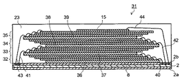
次に、本発明の第2の実施形態による半導体メモリカードについて、図5を参照して説明する。図5は第2の実施形態による半導体メモリカードの構成を示す断面図(メモリカードを短辺方向に切断した断面図)である。図5に示される半導体メモリカード31は第1の実施形態と同様に、マイクロSDTM規格のメモリカード等として使用される。半導体メモリカード31の平面構造は基本的には図1と同様であるため、ここでは図示を省略する。メモリカード31の平面構造の説明に関しては図1を参照するものとする。また、第1の実施形態と同一部分には同一符号を付し、その説明を一部省略する。 Next, a semiconductor memory card according to a second embodiment of the present invention will be described with reference to FIG. FIG. 5 is a cross-sectional view showing the configuration of the semiconductor memory card according to the second embodiment (cross-sectional view of the memory card cut in the short side direction). The semiconductor memory card 31 shown in FIG. 5 is used as a micro SD ™ standard memory card or the like as in the first embodiment. Since the planar structure of the semiconductor memory card 31 is basically the same as that of FIG. 1, the illustration thereof is omitted here. Refer to FIG. 1 for the description of the planar structure of the memory card 31. The same parts as those in the first embodiment are denoted by the same reference numerals, and a part of the description is omitted.
半導体メモリカード31は、配線基板2の素子搭載部8上に配置された第1の素子群32、第2の素子群33、第3の素子群34および第4の素子群35を具備している。配線基板2の第2の面2b上には、第1の素子群32を構成する4個のメモリ素子36が階段状に積層されている。第1の素子群32は第1の実施形態の第1の素子群13と同様な構成を有している。第1の素子群32上には、第2の素子群33を構成する4個のメモリ素子37が第1の素子群32と逆方向に向けて階段状に積層されている。第2の素子群33は第1の実施形態の第2の素子群14と同様な構成を有している。
The semiconductor memory card 31 includes a
第2の素子群33上には第3の素子群34を構成する4個のメモリ素子38が積層されている。第3の素子群34は第1の素子群32と同様な構成を有している。第3の素子群34を構成するメモリ素子38は、第1の素子群32と同方向で、かつ第2の素子群32と逆方向に向けて階段状に積層されている。第3の素子群34上には第4の素子群35を構成する4個のメモリ素子39が積層されている。第4の素子群35は第2の素子群33と同様な構成を有している。第4の素子群35を構成するメモリ素子39は、第2の素子群33と同方向で、かつ第3の素子群34と逆方向に向けて階段状に積層されている。
Four
第1ないし第4の素子群32〜35を構成するメモリ素子36〜39の電極パッドは、それぞれ第1ないし第4の金属ワイヤ40〜43を介して配線基板2の接続パッドと電気的に接続されている。さらに、第4の素子群35上にはコントローラ素子15が配置されている。コントローラ素子15は第5の金属ワイヤ44を介して配線基板2の接続パッドと電気的に接続されている。メモリ素子36〜39やコントローラ素子15の電極パッドの配列形状等の構成は第1の実施形態と同様とされている。
The electrode pads of the
このように、配線基板2上に配置する素子群32〜35の階段状積層方向(メモリ素子を階段状に積層する際のずらし方向)を順に逆方向することによって、配線基板2の素子占有面積を増加させることなく素子群32〜35の数を増やすことができる。従って、配線基板2の素子搭載面積(実用的に素子の搭載が可能な面積)内に配置するメモリ素子数を増加させることが可能となる。すなわち、小型・高容量の高いメモリカード31を提供することができる。例えば、多値技術の適用等で2GBの記憶容量を実現したメモリ素子36〜39を合計16個使用することによって、32GBのマイクロSDTMカード(半導体メモリカード31)を実現することが可能となる。
In this way, the element occupation area of the
上述した実施形態のメモリカード1、31はそれら単体で構成するケースレスの半導体メモリカードに対して有効であるが、必ずしもベースカードのようなケースを用いた半導体メモリカードを除外するものではない。さらに、実施形態の半導体メモリカードの構造は、場合によってはメモリカード以外の半導体記憶装置にも適用できる。実施形態の装置構造はBGAパッケージ構造やLGAパッケージ構造を有する半導体記憶装置にも適用可能である。半導体パッケージは配線基板に半田ボール等からなる外部接続端子(ボール端子)が設けられることを除いて、基本的な構造はメモリカードと同様とされる。 The memory cards 1 and 31 according to the above-described embodiments are effective for a caseless semiconductor memory card configured as a single unit, but do not necessarily exclude a semiconductor memory card using a case such as a base card. Furthermore, the structure of the semiconductor memory card of the embodiment can be applied to a semiconductor memory device other than the memory card depending on circumstances. The device structure of the embodiment can also be applied to a semiconductor memory device having a BGA package structure or an LGA package structure. The basic structure of a semiconductor package is the same as that of a memory card except that an external connection terminal (ball terminal) made of a solder ball or the like is provided on a wiring board.
なお、本発明の半導体メモリカードは上記した実施形態に限定されるものではなく、長辺片側パッド構造を有するメモリ素子で構成した複数のメモリ素子群を配線基板上に搭載した各種の半導体メモリカードに適用可能である。本発明の半導体メモリカードの具体的な構造は、本発明の基本構成を満足するものであれば種々に変形が可能である。さらに、実施形態は本発明の技術的思想の範囲内で拡張もしくは変更することができ、拡張、変更した実施形態も本発明の技術的範囲に含まれるものである。 The semiconductor memory card of the present invention is not limited to the above-described embodiment, and various semiconductor memory cards in which a plurality of memory element groups each composed of a memory element having a long-side one-side pad structure are mounted on a wiring board. It is applicable to. The specific structure of the semiconductor memory card of the present invention can be variously modified as long as it satisfies the basic configuration of the present invention. Furthermore, the embodiments can be expanded or modified within the scope of the technical idea of the present invention, and the expanded and modified embodiments are also included in the technical scope of the present invention.
1,31…メモリカード、2…配線基板、2a…第1の面、2b…第2の面、4A…第1の短辺、4B…第2の短辺、5A…第1の長辺、5B…第2の長辺、6…切り欠き部、7…くびれ部、8…素子搭載部、9…接続パッド、10,10A〜10D…パッド領域,11,11A〜11D,12,12A〜12D,36,37,38,39…メモリ素子、13,14,32,33,34,35…素子群、15…コントローラ素子、16,19,21A,21B…電極パッド、18,20,22,40,41,42,43,44…金属ワイヤ、23…封止樹脂層。 DESCRIPTION OF SYMBOLS 1,31 ... Memory card, 2 ... Wiring board, 2a ... 1st surface, 2b ... 2nd surface, 4A ... 1st short side, 4B ... 2nd short side, 5A ... 1st long side, 5B ... 2nd long side, 6 ... Notch part, 7 ... Constriction part, 8 ... Element mounting part, 9 ... Connection pad, 10, 10A-10D ... Pad area | region, 11, 11A-11D, 12, 12A-12D , 36, 37, 38, 39 ... memory elements, 13, 14, 32, 33, 34, 35 ... element groups, 15 ... controller elements, 16, 19, 21A, 21B ... electrode pads, 18, 20, 22, 40 , 41, 42, 43, 44 ... metal wire, 23 ... sealing resin layer.
Claims (6)
長辺に沿って配列された電極パッドを有する複数の第1のメモリ素子を備え、前記複数の第1のメモリ素子は前記長辺が前記配線基板の前記第1のパッド領域の近傍に位置すると共に前記電極パッドが露出するように、前記配線基板の前記素子搭載部上に階段状に積層されている第1の素子群と;
長辺に沿って配列された電極パッドを有する複数の第2のメモリ素子を備え、前記複数の第2のメモリ素子は前記長辺が前記配線基板の前記第2のパッド領域の近傍に位置すると共に前記電極パッドが露出するように、前記第1の素子群上に前記第1の素子群の階段方向とは逆方向に向けて階段状に積層されている第2の素子群と;
前記第2の素子群上に配置され、少なくとも一つの外形辺に沿って配列された電極パッドを有するコントローラ素子と;
前記第1のパッド領域に配置された前記接続パッドと前記複数の第1のメモリ素子の前記電極パッドとを電気的に接続する第1の金属ワイヤと;
前記第2のパッド領域に配置された前記接続パッドと前記複数の第2のメモリ素子の前記電極パッドとを電気的に接続する第2の金属ワイヤと;
前記配線基板の前記接続パッドと前記コントローラ素子の前記電極パッドとを電気的に接続する第3の金属ワイヤと;
前記第1および第2の素子群と前記コントローラ素子とを前記第1ないし第3の金属ワイヤと共に封止するように、前記配線基板の前記第2の面上に形成された封止樹脂層とを具備し、
前記配線基板は前記第1の長辺に設けられた切り欠き部を有し、前記第1のパッド領域は前記第1の長辺の前記切り欠き部を除く部分に沿って設けられており、かつ前記第1のメモリ素子の前記電極パッドは前記配線基板の前記第1のパッド領域と対応するように偏った配列形状を有し、
前記第2のメモリ素子の前記電極パッドは前記第1のメモリ素子と同一の偏った配列形状を有し、前記第2のメモリ素子は前記第1のメモリ素子とは反転した状態で配置されており、かつ前記配線基板の前記第2のパッド領域は前記第2のメモリ素子の前記電極パッドの配列形状に対応するように配置された前記接続パッドを有し、
前記第2の素子群における最下段の前記第2のメモリ素子はそれ以外の前記第2のメモリより厚い厚さを有し、
前記第1および第2のメモリ素子の角部近傍に位置する前記電極パッドの少なくとも一部は前記配線基板の短辺に沿って設けられたパッド領域に配置された前記接続パッドと電気的に接続されていることを特徴とする半導体メモリカード。 A substantially rectangular outer shape, a first surface provided with external connection terminals, an element mounting portion, a first pad region at least along the first long side, and a second pad along the second long side A wiring board having a second surface comprising connection pads disposed in the region;
A plurality of first memory elements having electrode pads arranged along a long side are provided, and the long sides of the plurality of first memory elements are located in the vicinity of the first pad region of the wiring board. And a first element group stacked stepwise on the element mounting portion of the wiring board so that the electrode pad is exposed;
A plurality of second memory elements having electrode pads arranged along a long side, wherein the plurality of second memory elements are positioned in the vicinity of the second pad region of the wiring board; And a second element group stacked on the first element group in a staircase pattern in a direction opposite to the staircase direction of the first element group so that the electrode pad is exposed;
A controller element having an electrode pad disposed on the second element group and arranged along at least one outer side;
A first metal wire that electrically connects the connection pad disposed in the first pad region and the electrode pads of the plurality of first memory elements;
A second metal wire that electrically connects the connection pad disposed in the second pad region and the electrode pads of the plurality of second memory elements;
A third metal wire for electrically connecting the connection pad of the wiring board and the electrode pad of the controller element;
A sealing resin layer formed on the second surface of the wiring board so as to seal the first and second element groups and the controller element together with the first to third metal wires; Comprising
The wiring board has a cutout portion provided on the first long side, and the first pad region is provided along a portion excluding the cutout portion of the first long side, In addition, the electrode pads of the first memory element have an array shape that is biased to correspond to the first pad region of the wiring board,
The electrode pads of the second memory element have the same biased array shape as the first memory element, and the second memory element is arranged in an inverted state with respect to the first memory element. And the second pad region of the wiring board has the connection pads arranged to correspond to the array shape of the electrode pads of the second memory element,
The lowermost second memory element in the second element group has a thickness greater than the other second memories,
At least a part of the electrode pads located near the corners of the first and second memory elements are electrically connected to the connection pads arranged in a pad region provided along the short side of the wiring board. A semiconductor memory card characterized by being made.
長辺に沿って配列された電極パッドを有し、前記長辺が前記配線基板の前記第1のパッド領域の近傍に位置するように、前記配線基板の前記素子搭載部上に配置された第1のメモリ素子と;
長辺に沿って配列された電極パッドを有し、前記長辺が前記配線基板の前記第2のパッド領域の近傍に位置するように、前記第1のメモリ素子上に配置された第2のメモリ素子と;
前記第2のメモリ上に配置され、少なくとも一つの外形辺に沿って配列された電極パッドを有するコントローラ素子と;
前記第1のパッド領域に配置された前記接続パッドと前記第1のメモリ素子の前記電極パッドとを電気的に接続する第1の金属ワイヤと;
前記第2のパッド領域に配置された前記接続パッドと前記第2のメモリ素子の前記電極パッドとを電気的に接続する第2の金属ワイヤと;
前記配線基板の前記接続パッドと前記コントローラ素子の前記電極パッドとを電気的に接続する第3の金属ワイヤと;
前記第1および第2のメモリ素子と前記コントローラ素子とを前記第1ないし第3の金属ワイヤと共に封止するように、前記配線基板の前記第2の面上に形成された封止樹脂層とを具備し、
前記配線基板は前記第1の長辺に設けられた切り欠き部を有し、前記第1のパッド領域は前記第1の長辺の前記切り欠き部を除く部分に沿って設けられており、かつ前記第1のメモリ素子の前記電極パッドは前記配線基板の前記第1のパッド領域と対応するように偏った配列形状を有することを特徴とする半導体メモリカード。 A first surface provided with an external connection terminal; an element mounting portion; and a connection pad disposed at least in a first pad region along the first long side and a second pad region along the second long side. A wiring board having a second surface comprising:
A first electrode disposed on the element mounting portion of the wiring board so as to have an electrode pad arranged along a long side, and the long side is located in the vicinity of the first pad region of the wiring board; One memory element;
A second electrode disposed on the first memory element, the electrode pad being arranged along a long side, wherein the long side is positioned in the vicinity of the second pad region of the wiring board; A memory element;
A controller element having an electrode pad disposed on the second memory and arranged along at least one outer edge;
A first metal wire that electrically connects the connection pad disposed in the first pad region and the electrode pad of the first memory element;
A second metal wire for electrically connecting the connection pad disposed in the second pad region and the electrode pad of the second memory element;
A third metal wire for electrically connecting the connection pad of the wiring board and the electrode pad of the controller element;
A sealing resin layer formed on the second surface of the wiring board so as to seal the first and second memory elements and the controller element together with the first to third metal wires; equipped with,
The wiring board has a cutout portion provided on the first long side, and the first pad region is provided along a portion excluding the cutout portion of the first long side, The semiconductor memory card according to claim 1, wherein the electrode pads of the first memory element have an array shape that is biased so as to correspond to the first pad region of the wiring board .
長辺に沿って配列された電極パッドを有する複数の第1のメモリ素子を備え、前記複数の第1のメモリ素子は前記長辺が前記配線基板の前記第1のパッド領域の近傍に位置すると共に前記電極パッドが露出するように、前記配線基板の前記素子搭載部上に階段状に積層されている第1の素子群と;
長辺に沿って配列された電極パッドを有する複数の第2のメモリ素子を備え、前記複数の第2のメモリ素子は前記長辺が前記配線基板の前記第2のパッド領域の近傍に位置すると共に前記電極パッドが露出するように、前記第1の素子群上に前記第1の素子群の階段方向とは逆方向に向けて階段状に積層されている第2の素子群と;
前記第2の素子群上に配置され、少なくとも一つの外形辺に沿って配列された電極パッドを有するコントローラ素子と;
前記第1のパッド領域に配置された前記接続パッドと前記複数の第1のメモリ素子の前記電極パッドとを電気的に接続する第1の金属ワイヤと;
前記第2のパッド領域に配置された前記接続パッドと前記複数の第2のメモリ素子の前記電極パッドとを電気的に接続する第2の金属ワイヤと;
前記配線基板の前記接続パッドと前記コントローラ素子の前記電極パッドとを電気的に接続する第3の金属ワイヤと;
前記第1および第2の素子群と前記コントローラ素子とを前記第1ないし第3の金属ワイヤと共に封止するように、前記配線基板の前記第2の面上に形成された封止樹脂層とを具備し、
前記配線基板は前記第1の長辺に設けられた切り欠き部を有し、前記第1のパッド領域は前記第1の長辺の前記切り欠き部を除く部分に沿って設けられており、かつ前記第1のメモリ素子の前記電極パッドは前記配線基板の前記第1のパッド領域と対応するように偏った配列形状を有することを特徴とする半導体メモリカード。 A substantially rectangular outer shape, a first surface provided with external connection terminals, an element mounting portion, a first pad region at least along the first long side, and a second pad along the second long side A wiring board having a second surface comprising connection pads disposed in the region;
A plurality of first memory elements having electrode pads arranged along a long side are provided, and the long sides of the plurality of first memory elements are located in the vicinity of the first pad region of the wiring board. And a first element group stacked stepwise on the element mounting portion of the wiring board so that the electrode pad is exposed;
A plurality of second memory elements having electrode pads arranged along a long side, wherein the plurality of second memory elements are positioned in the vicinity of the second pad region of the wiring board; And a second element group stacked on the first element group in a staircase pattern in a direction opposite to the staircase direction of the first element group so that the electrode pad is exposed;
A controller element having an electrode pad disposed on the second element group and arranged along at least one outer side;
A first metal wire that electrically connects the connection pad disposed in the first pad region and the electrode pads of the plurality of first memory elements;
A second metal wire that electrically connects the connection pad disposed in the second pad region and the electrode pads of the plurality of second memory elements;
A third metal wire for electrically connecting the connection pad of the wiring board and the electrode pad of the controller element;
A sealing resin layer formed on the second surface of the wiring board so as to seal the first and second element groups and the controller element together with the first to third metal wires; equipped with,
The wiring board has a cutout portion provided on the first long side, and the first pad region is provided along a portion excluding the cutout portion of the first long side, The semiconductor memory card according to claim 1, wherein the electrode pads of the first memory element have an array shape that is biased so as to correspond to the first pad region of the wiring board .
前記第2の素子群における最下段の前記第2のメモリ素子はそれ以外の前記第2のメモリより厚い厚さを有することを特徴とする半導体メモリカード。 The semiconductor memory card according to claim 3,
2. The semiconductor memory card according to claim 1, wherein the second memory element at the lowest stage in the second element group has a thickness greater than that of the other second memories.
前記第2のメモリ素子の前記電極パッドは前記第1のメモリ素子と同一の偏った配列形状を有し、前記第2のメモリ素子は前記第1のメモリ素子とは反転した状態で配置されており、かつ前記配線基板の前記第2のパッド領域は前記第2のメモリ素子の前記電極パッドの配列形状に対応するように配置された前記接続パッドを有することを特徴とする半導体メモリカード。 The semiconductor memory card according to any one of claims 2 to 4 ,
The electrode pads of the second memory element have the same biased array shape as the first memory element, and the second memory element is arranged in an inverted state with respect to the first memory element. And the second pad area of the wiring board has the connection pads arranged to correspond to the arrangement shape of the electrode pads of the second memory element.
前記第1および第2のメモリ素子の角部近傍に位置する前記電極パッドの少なくとも一部は前記配線基板の短辺に沿って設けられたパッド領域に配置された前記接続パッドと電気的に接続されていることを特徴とする半導体メモリカード。 The semiconductor memory card according to any one of claims 2 to 5 ,
At least a part of the electrode pads located near the corners of the first and second memory elements are electrically connected to the connection pads arranged in a pad region provided along the short side of the wiring board. A semiconductor memory card characterized by being made.
Priority Applications (4)
| Application Number | Priority Date | Filing Date | Title |
|---|---|---|---|
| JP2008280713A JP4776675B2 (en) | 2008-10-31 | 2008-10-31 | Semiconductor memory card |
| US12/558,814 US7855446B2 (en) | 2008-10-31 | 2009-09-14 | Semiconductor memory device and semiconductor memory card |
| US12/939,210 US8080868B2 (en) | 2008-10-31 | 2010-11-04 | Semiconductor memory device and semiconductor memory card |
| US13/288,423 US8288855B2 (en) | 2008-10-31 | 2011-11-03 | Semiconductor memory device and semiconductor memory card |
Applications Claiming Priority (1)
| Application Number | Priority Date | Filing Date | Title |
|---|---|---|---|
| JP2008280713A JP4776675B2 (en) | 2008-10-31 | 2008-10-31 | Semiconductor memory card |
Publications (3)
| Publication Number | Publication Date |
|---|---|
| JP2010109206A JP2010109206A (en) | 2010-05-13 |
| JP2010109206A5 JP2010109206A5 (en) | 2011-02-03 |
| JP4776675B2 true JP4776675B2 (en) | 2011-09-21 |
Family
ID=42130383
Family Applications (1)
| Application Number | Title | Priority Date | Filing Date |
|---|---|---|---|
| JP2008280713A Expired - Fee Related JP4776675B2 (en) | 2008-10-31 | 2008-10-31 | Semiconductor memory card |
Country Status (2)
| Country | Link |
|---|---|
| US (3) | US7855446B2 (en) |
| JP (1) | JP4776675B2 (en) |
Families Citing this family (42)
| Publication number | Priority date | Publication date | Assignee | Title |
|---|---|---|---|---|
| US7691668B2 (en) * | 2006-12-19 | 2010-04-06 | Spansion Llc | Method and apparatus for multi-chip packaging |
| US8004071B2 (en) | 2007-12-27 | 2011-08-23 | Kabushiki Kaisha Toshiba | Semiconductor memory device |
| US8476749B2 (en) * | 2009-07-22 | 2013-07-02 | Oracle America, Inc. | High-bandwidth ramp-stack chip package |
| US20110084374A1 (en) * | 2009-10-08 | 2011-04-14 | Jen-Chung Chen | Semiconductor package with sectioned bonding wire scheme |
| US9401745B1 (en) | 2009-12-11 | 2016-07-26 | Micron Technology, Inc. | Wireless communication link using near field coupling |
| JP5512292B2 (en) * | 2010-01-08 | 2014-06-04 | ルネサスエレクトロニクス株式会社 | Manufacturing method of semiconductor device |
| US8283766B2 (en) * | 2010-09-02 | 2012-10-09 | Oracle America, Inc | Ramp-stack chip package with static bends |
| KR20120024099A (en) * | 2010-09-06 | 2012-03-14 | 삼성전자주식회사 | Multi-chip package and method of manufacturing the same |
| JP2012212417A (en) * | 2011-03-24 | 2012-11-01 | Toshiba Corp | Semiconductor memory card |
| JP6122290B2 (en) * | 2011-12-22 | 2017-04-26 | 三星電子株式会社Samsung Electronics Co.,Ltd. | Semiconductor package having a rewiring layer |
| US9082632B2 (en) | 2012-05-10 | 2015-07-14 | Oracle International Corporation | Ramp-stack chip package with variable chip spacing |
| JP5768068B2 (en) * | 2013-01-18 | 2015-08-26 | 株式会社東芝 | Image erasing device |
| USD758372S1 (en) * | 2013-03-13 | 2016-06-07 | Nagrastar Llc | Smart card interface |
| USD759022S1 (en) * | 2013-03-13 | 2016-06-14 | Nagrastar Llc | Smart card interface |
| WO2014156921A1 (en) * | 2013-03-26 | 2014-10-02 | ピーエスフォー ルクスコ エスエイアールエル | Semiconductor device |
| KR102122460B1 (en) * | 2013-07-17 | 2020-06-12 | 삼성전자주식회사 | Semiconductor package |
| JP5996500B2 (en) * | 2013-09-11 | 2016-09-21 | 株式会社東芝 | Semiconductor device and memory device |
| KR102144367B1 (en) * | 2013-10-22 | 2020-08-14 | 삼성전자주식회사 | Semiconductor package and method of fabricating the same |
| USD730910S1 (en) * | 2014-05-02 | 2015-06-02 | Samsung Electronics Co., Ltd. | Memory card |
| USD730907S1 (en) * | 2014-05-02 | 2015-06-02 | Samsung Electronics Co., Ltd. | Memory card |
| USD730908S1 (en) * | 2014-05-02 | 2015-06-02 | Samsung Electronics Co., Ltd. | Memory card |
| USD729251S1 (en) * | 2014-06-27 | 2015-05-12 | Samsung Electronics Co., Ltd. | Memory card |
| USD730909S1 (en) * | 2014-06-27 | 2015-06-02 | Samsung Electronics Co., Ltd. | Memory card |
| USD727912S1 (en) * | 2014-06-27 | 2015-04-28 | Samsung Electronics Co., Ltd. | Memory card |
| USD727913S1 (en) * | 2014-06-27 | 2015-04-28 | Samsung Electronics Co., Ltd. | Memory card |
| USD727911S1 (en) * | 2014-06-27 | 2015-04-28 | Samsung Electronics Co., Ltd. | Memory card |
| USD736214S1 (en) * | 2014-07-01 | 2015-08-11 | Samsung Electronics Co., Ltd. | Memory card |
| USD736212S1 (en) * | 2014-07-01 | 2015-08-11 | Samsung Electronics Co., Ltd. | Memory card |
| USD736215S1 (en) * | 2014-07-01 | 2015-08-11 | Samsung Electronics Co., Ltd. | Memory card |
| USD727910S1 (en) * | 2014-07-02 | 2015-04-28 | Samsung Electronics Co., Ltd. | Memory card |
| USD864968S1 (en) | 2015-04-30 | 2019-10-29 | Echostar Technologies L.L.C. | Smart card interface |
| USD773466S1 (en) * | 2015-08-20 | 2016-12-06 | Isaac S. Daniel | Combined secure digital memory and subscriber identity module |
| USD798868S1 (en) * | 2015-08-20 | 2017-10-03 | Isaac S. Daniel | Combined subscriber identification module and storage card |
| USD783621S1 (en) * | 2015-08-25 | 2017-04-11 | Samsung Electronics Co., Ltd. | Memory card |
| USD783622S1 (en) * | 2015-08-25 | 2017-04-11 | Samsung Electronics Co., Ltd. | Memory card |
| US11171114B2 (en) * | 2015-12-02 | 2021-11-09 | Intel Corporation | Die stack with cascade and vertical connections |
| US10153221B1 (en) * | 2017-06-13 | 2018-12-11 | Micron Technology, Inc. | Face down dual sided chip scale memory package |
| KR102591697B1 (en) * | 2019-03-06 | 2023-10-20 | 에스케이하이닉스 주식회사 | Stack package including hybrid wire bonding structures |
| JP2021089932A (en) * | 2019-12-03 | 2021-06-10 | キオクシア株式会社 | Semiconductor storage device |
| US11309288B2 (en) * | 2020-04-08 | 2022-04-19 | Nanya Technology Corporation | Electronic system, die assembly and device die |
| CN112614915B (en) * | 2020-12-29 | 2022-03-08 | 江苏宜兴德融科技有限公司 | Solar cell testing method and solar cell testing intermediate structure |
| CN113380755B (en) * | 2021-06-11 | 2023-07-25 | 西安微电子技术研究所 | Multilayer chip stack assembly packaging structure and preparation process thereof |
Family Cites Families (28)
| Publication number | Priority date | Publication date | Assignee | Title |
|---|---|---|---|---|
| JPH04302164A (en) * | 1991-03-29 | 1992-10-26 | Fujitsu Ltd | Semiconductor device |
| JP3172473B2 (en) * | 1997-09-08 | 2001-06-04 | 三洋電機株式会社 | Semiconductor device |
| US6621155B1 (en) * | 1999-12-23 | 2003-09-16 | Rambus Inc. | Integrated circuit device having stacked dies and impedance balanced transmission lines |
| JP3768761B2 (en) | 2000-01-31 | 2006-04-19 | 株式会社日立製作所 | Semiconductor device and manufacturing method thereof |
| US6900528B2 (en) * | 2001-06-21 | 2005-05-31 | Micron Technology, Inc. | Stacked mass storage flash memory package |
| JP4068974B2 (en) * | 2003-01-22 | 2008-03-26 | 株式会社ルネサステクノロジ | Semiconductor device |
| JP2005302871A (en) | 2004-04-08 | 2005-10-27 | Toshiba Corp | Laminated semiconductor device and its manufacturing method |
| US7190068B2 (en) * | 2004-06-25 | 2007-03-13 | Intel Corporation | Bottom heat spreader |
| JP4759948B2 (en) * | 2004-07-28 | 2011-08-31 | ルネサスエレクトロニクス株式会社 | Manufacturing method of semiconductor device |
| JP2007004775A (en) * | 2005-05-23 | 2007-01-11 | Toshiba Corp | Semiconductor memory card |
| JP2007128953A (en) * | 2005-11-01 | 2007-05-24 | Toshiba Corp | Semiconductor device and memory card using same |
| JP2007134486A (en) * | 2005-11-10 | 2007-05-31 | Toshiba Corp | Stacked semiconductor device and its manufacturing method |
| JP4726640B2 (en) * | 2006-01-20 | 2011-07-20 | ルネサスエレクトロニクス株式会社 | Semiconductor device |
| JP4843447B2 (en) | 2006-03-31 | 2011-12-21 | 株式会社東芝 | Semiconductor device and memory card using the same |
| US7550834B2 (en) * | 2006-06-29 | 2009-06-23 | Sandisk Corporation | Stacked, interconnected semiconductor packages |
| US7592691B2 (en) * | 2006-09-01 | 2009-09-22 | Micron Technology, Inc. | High density stacked die assemblies, structures incorporated therein and methods of fabricating the assemblies |
| TW200814249A (en) * | 2006-09-12 | 2008-03-16 | Chipmos Technologies Inc | Stacked chip package structure with lead-frame having bus bar |
| JP4921937B2 (en) * | 2006-11-24 | 2012-04-25 | 株式会社東芝 | Semiconductor integrated circuit |
| US8242607B2 (en) * | 2006-12-20 | 2012-08-14 | Stats Chippac Ltd. | Integrated circuit package system with offset stacked die and method of manufacture thereof |
| TWI327365B (en) * | 2007-01-19 | 2010-07-11 | Chipmos Technologies Inc | Zigzag-stacked chip package structure |
| JP4498403B2 (en) | 2007-09-28 | 2010-07-07 | 株式会社東芝 | Semiconductor device and semiconductor memory device |
| KR100886717B1 (en) * | 2007-10-16 | 2009-03-04 | 주식회사 하이닉스반도체 | Stacked semiconductor package and method of manufacturing thereof |
| JP2009164160A (en) * | 2007-12-28 | 2009-07-23 | Panasonic Corp | Semiconductor device laminate and packaging method |
| JP2009205613A (en) * | 2008-02-29 | 2009-09-10 | Toshiba Corp | Semiconductor memory apparatus |
| JP5700927B2 (en) * | 2008-11-28 | 2015-04-15 | 新光電気工業株式会社 | Semiconductor device and manufacturing method of semiconductor device |
| JP2010165984A (en) * | 2009-01-19 | 2010-07-29 | Toshiba Corp | Semiconductor device |
| JP2010278318A (en) * | 2009-05-29 | 2010-12-09 | Renesas Electronics Corp | Semiconductor device |
| KR101563630B1 (en) * | 2009-09-17 | 2015-10-28 | 에스케이하이닉스 주식회사 | Semiconductor package |
-
2008
- 2008-10-31 JP JP2008280713A patent/JP4776675B2/en not_active Expired - Fee Related
-
2009
- 2009-09-14 US US12/558,814 patent/US7855446B2/en active Active
-
2010
- 2010-11-04 US US12/939,210 patent/US8080868B2/en active Active
-
2011
- 2011-11-03 US US13/288,423 patent/US8288855B2/en active Active
Also Published As
| Publication number | Publication date |
|---|---|
| US8288855B2 (en) | 2012-10-16 |
| US7855446B2 (en) | 2010-12-21 |
| JP2010109206A (en) | 2010-05-13 |
| US8080868B2 (en) | 2011-12-20 |
| US20100109141A1 (en) | 2010-05-06 |
| US20110042467A1 (en) | 2011-02-24 |
| US20120043671A1 (en) | 2012-02-23 |
Similar Documents
| Publication | Publication Date | Title |
|---|---|---|
| JP4776675B2 (en) | Semiconductor memory card | |
| JP5193837B2 (en) | Semiconductor memory card | |
| JP4498403B2 (en) | Semiconductor device and semiconductor memory device | |
| US8395268B2 (en) | Semiconductor memory device | |
| US8064206B2 (en) | Semiconductor memory device and semiconductor memory card using the same | |
| JP5150243B2 (en) | Semiconductor memory device | |
| JP2009205613A (en) | Semiconductor memory apparatus | |
| US20100187690A1 (en) | Semiconductor device | |
| JP2008311559A (en) | Semiconductor package | |
| US8603865B2 (en) | Semiconductor storage device and manufacturing method thereof | |
| TWI529918B (en) | Semiconductor memory card | |
| JP5150242B2 (en) | Semiconductor memory device | |
| JP5178213B2 (en) | Stacked semiconductor device and semiconductor memory device | |
| KR20110055985A (en) | Stack package | |
| JP2010232702A (en) | Laminated semiconductor device | |
| JP2009194294A (en) | Laminated semiconductor device | |
| JP4489094B2 (en) | Semiconductor package | |
| JP5184951B2 (en) | Semiconductor package | |
| JP2012093941A (en) | Memory card |
Legal Events
| Date | Code | Title | Description |
|---|---|---|---|
| A521 | Request for written amendment filed |
Free format text: JAPANESE INTERMEDIATE CODE: A523 Effective date: 20101209 |
|
| A621 | Written request for application examination |
Free format text: JAPANESE INTERMEDIATE CODE: A621 Effective date: 20101209 |
|
| A871 | Explanation of circumstances concerning accelerated examination |
Free format text: JAPANESE INTERMEDIATE CODE: A871 Effective date: 20110104 |
|
| A975 | Report on accelerated examination |
Free format text: JAPANESE INTERMEDIATE CODE: A971005 Effective date: 20110120 |
|
| A131 | Notification of reasons for refusal |
Free format text: JAPANESE INTERMEDIATE CODE: A131 Effective date: 20110222 |
|
| A521 | Request for written amendment filed |
Free format text: JAPANESE INTERMEDIATE CODE: A523 Effective date: 20110425 |
|
| RD02 | Notification of acceptance of power of attorney |
Free format text: JAPANESE INTERMEDIATE CODE: A7422 Effective date: 20110425 |
|
| TRDD | Decision of grant or rejection written | ||
| A01 | Written decision to grant a patent or to grant a registration (utility model) |
Free format text: JAPANESE INTERMEDIATE CODE: A01 Effective date: 20110607 |
|
| A01 | Written decision to grant a patent or to grant a registration (utility model) |
Free format text: JAPANESE INTERMEDIATE CODE: A01 |
|
| A61 | First payment of annual fees (during grant procedure) |
Free format text: JAPANESE INTERMEDIATE CODE: A61 Effective date: 20110628 |
|
| R151 | Written notification of patent or utility model registration |
Ref document number: 4776675 Country of ref document: JP Free format text: JAPANESE INTERMEDIATE CODE: R151 |
|
| FPAY | Renewal fee payment (event date is renewal date of database) |
Free format text: PAYMENT UNTIL: 20140708 Year of fee payment: 3 |
|
| S111 | Request for change of ownership or part of ownership |
Free format text: JAPANESE INTERMEDIATE CODE: R313111 |
|
| R350 | Written notification of registration of transfer |
Free format text: JAPANESE INTERMEDIATE CODE: R350 |
|
| S111 | Request for change of ownership or part of ownership |
Free format text: JAPANESE INTERMEDIATE CODE: R313111 |
|
| R350 | Written notification of registration of transfer |
Free format text: JAPANESE INTERMEDIATE CODE: R350 |
|
| LAPS | Cancellation because of no payment of annual fees |