JP4765201B2 - OVD seal and manufacturing method thereof - Google Patents
OVD seal and manufacturing method thereof Download PDFInfo
- Publication number
- JP4765201B2 JP4765201B2 JP2001172428A JP2001172428A JP4765201B2 JP 4765201 B2 JP4765201 B2 JP 4765201B2 JP 2001172428 A JP2001172428 A JP 2001172428A JP 2001172428 A JP2001172428 A JP 2001172428A JP 4765201 B2 JP4765201 B2 JP 4765201B2
- Authority
- JP
- Japan
- Prior art keywords
- ovd
- layer
- seal
- resins
- adhesive
- Prior art date
- Legal status (The legal status is an assumption and is not a legal conclusion. Google has not performed a legal analysis and makes no representation as to the accuracy of the status listed.)
- Expired - Fee Related
Links
Images


Landscapes
- Adhesive Tapes (AREA)
- Adhesives Or Adhesive Processes (AREA)
- Diffracting Gratings Or Hologram Optical Elements (AREA)
- Holo Graphy (AREA)
Description
【0001】
【発明の属する技術分野】
本発明は、貼り替えを防止に有効な技術であり、特に、近年ブランドプロテクション等の認証に用いられているホログラムをはじめとする光の方向により色彩や画像が変化するOVDを利用したOVDシールに関する。
【従来の技術】
【0002】
近年、光の干渉を用いて立体画像や特殊な装飾画像を表現し得る、ホログラム、回折格子、あるいは光学特性の異なる薄膜を重ねることにより見る角度によって色の変化(カラーシフト)を生じる光学的多層薄膜に代表されるようなOVD(OpticalVariableDeviceの略称)の開発が少なからず各地で進められている。
【0003】
これらOVDは立体画像やカラーシフトといった独特な印象を与えるため、優れた装飾効果を有しており各種包装材や絵本、カタログ等の一般的な印刷物に利用されてきた。
また、このOVDは高度な製造技術を要することから有効な偽造防止手段としてクレジットカード、有価証券、証明書類等の一部にあるいは全面に形成され使用されている。
最近では、有価証券以外にもスポーツ用品やコンピュータ部品をはじめとする電気製品ソフトウエアー等に貼り付けられ、その製品の真正さを証明する認証シールや、それら商品のパッケージに貼りつけられる封印シールとしても広く使われるようになってきた。
【0004】
【発明が解決しようとする課題】
これらのいわゆる認証シールや封印シールは、いったん剥がした後に、別の商品(不正をはたらく場合は普通は偽物品)の上に貼り替えられるという偽造が心配されるので、剥離したとするとどこかが破壊してしまういわゆる脆性タイプのシールが提案されてきた。例えば、実用新案登録第2032258号によると、その構成の一部に脆質な材料を用いた層が設けてあり、無理に剥がそうとすると、その脆質な材料を用いた層の部分の破壊をきっかけとして、破壊が広がることを特徴としている。
しかしながら、このような手法は、例えば、市販のラベル剥離剤(シール剥がし液等)を用いて粘着剤を冒すことによって、容易に剥がされる場合もあるという欠点(問題点)を有している。
【0005】
本発明は前記従来の技術の持つ問題点に鑑みてなされたものであり、その目的は、例えば市販のラベル剥離剤によって粘着剤を冒して不正行為を行なおうと試みても、それに伴う貼り替えを防ぐなど、貼り替えによる不正行為を許さないことに有効なOVDシールとその製造方法を提供することにある。
【0006】
【課題を解決するための手段】
前記課題を解決するために本発明が提供する手段は、まず、高分子樹脂材料を用いてある支持体に、OVD層および接着層の少なくとも2層がこの順で積層してあるOVDシールであって、
該接着層の一部か又はそのすべてに、硬化性樹脂を用いてあることを特徴とするOVDシールである。(請求項1)
【0007】
また、前記接着層には、電子線照射により硬化する樹脂を用いてあることを特徴とする請求項1に記載のOVDシールである。(請求項2)
これによると、短時間に硬化させ容易に貼りつけることが可能である。
【0008】
請求項1又は2のいずれかに記載のOVDシールであって、前記OVD層が該OVDシールの面の中に部分的に設けてあることを特徴とする。(請求項3)
これによると、支持体側から容易に接着剤を硬化させることを可能とする。
【0009】
前記支持体と前記OVD層との間が剥離し易くしてあることを特徴とする請求項1乃至3のいずれかにOVDシールである。(請求項4)
これによると、無理やり剥がそうとすると支持体だけ剥がれて破壊してしまう。
【0010】
前記支持体と前記OVD層との間が、剥離し易い部分と剥離し難い部分とが設けてあることを特徴とする請求項1乃至3のいずれかにOVDシールである。(請求項5)
これによると、剥がそうとした際に部分的に破壊を生じさせ、元に戻そうとしても復元不可能な状態と成ってしまう構成である。
【0011】
前記OVD層と前記接着剤層との間が、剥離し易い部分と剥離し難い部分とが設けてあることを特徴とする請求項1乃至5のいずれかに記載のOVDシールである。(請求項6)
【0012】
高分子樹脂材料を用いてある支持体に、OVD層および接着層の少なくとも2層がこの順で積層するOVDシールの製造方法であって、
該接着層の一部か又はそのすべてに、硬化性樹脂を用いることを特徴とするOVDシールの製造方法である。(請求項7)
【0013】
総じて、本発明は、接着層を硬化性樹脂を主成分にしており、市販のラベル剥離剤において剥がすことが困難な、あるいは、剥がそうとしてもどこかが破壊してしまい、貼り替え防止に有効なOVDシールを提供する。
【0014】
【発明の実施の形態】
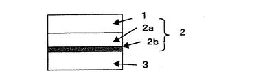
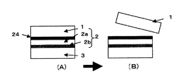
図1は本発明の貼り換え防止シールの基本構成を示す断面図である。図2、図3、および図4は、いずれも本発明の貼り替え防止シールの一構成例を示す図である。図中Aは剥がされる前の状態であり、図中Bは剥がされて破壊されたときの状態を示す図である。
以下では、これらの図面を参照しつつ、本発明をより詳細に説明する。
【0015】
図1に示した貼り替え防止シール11は、支持体1、OVD層2、接着層3を順次積層してなっている。図2、3、4は、剥がそうとすると完全に破壊するタイプのシールであり、それぞれ層間で剥離しやすい剥離層24を全面あるいは部分的に設けてなる。
【0016】
基材1はシール加工時における熱圧で軟化変形しない耐熱性と強度があれば良い。その材料としては、ポリ塩化ビニル、ポリエステル、ポリカーボネート、ポリメタクリル酸メチル、ポリスチレン、ポリエチレン、ポリエチレンテレフタレート、ポリエチレンナフタレート、ポリプロピレン、ポリビニルアルコール等の合成樹脂、天然樹脂、紙、合成紙などから単独あるいは複合体使用可能である。
また、上記の強靭なフィルムに柔らかい熱可塑性樹脂をコーティングし、加工の中間品あるいはシールを基材に貼りつけた後にフィルム部分を取り除くことも可能である。
その厚みは、操作性、加工性を考慮し2〜25μm程度のものが好ましい。
【0017】
次にOVD層2に関して説明する。
OVDとは光の干渉や回折を利用した画像であり、立体画像の表現や見る角度により色が変化するカラーシフトを生じる表示体である。その中でホログラムや回折格子のごときOVDとしては、光の干渉縞を微細な凹凸パターンとして平面に記録するレリーフ型や体積方向に干渉縞を記録する体積型が挙げられる。一方、ホログラムや回折格子と手法が異なり、光学特性の異なるセラミックスや金属材料の薄膜を積層し、見る角度により色の変化(カラーシフト)を生じる多層膜方式もその例である。
これら、OVDの中でも量産性やコストを考慮した場合には、レリーフ型ホログラム(回折格子)や多層薄膜方式のものが好ましく、一般にこれらのOVDが広く利用されている。
【0018】
レリーフ型のホログラム(回折格子)は光学的な撮影方式により、微細な凹凸パターンからなるレリーフ型のマスター版を作製し、電気メッキ法によりパターンを複製したニッケル製のプレス版にて量産を行う。すなわち、このプレス版を加熱しOVD形成層2aに押し当て、凹凸パターンを複製する。
【0019】
OVD形成層2aは、プレス版にて成形可能であるという性能が要求され、その材質は熱可塑性樹脂、熱硬化性樹脂、紫外線あるいは電子線硬化性樹脂のいずれであっても良い。例を挙げれば、アクリル系樹脂、エポキシ系樹脂、セルロース系樹脂、ビニル系樹脂等の熱可塑性樹脂や、反応性水酸基を有するアクリルポリオールやポリエステルポリオール等にポリイソシアネートを架橋剤として添加、架橋したウレタン樹脂や、メラミン系樹脂、フェノール系樹脂等の熱硬化樹脂、エポキシ(メタ)アクリル、ウレタン(メタ)アクリレート等の紫外線あるいは電子線硬化樹脂を単独もしくはこれらを複合して使用できる。また上記以外のものであっても、OVD画像を形成可能である公知の材料であれば、使用可能である。
【0020】
OVD効果層2bはOVD画像の回折効率を高めるためレリーフ面を構成する高分子材料と屈折率の異なる材料からなる。用いる材料としては、屈折率の異なるTiO2、Si2O3、SiO、Fe2O3、ZnS、などの高屈折率材料やより反射効果の高いAl、Sn、Cr、Ni、Cu、Au等の金属材料が挙げられ、これら材料を単独あるいは積層して使用できる。
これらの材料は真空蒸着法、スパッタリング等の公知の薄膜形成技術にて形成され、その膜厚は用途によって異なるが、50〜10000Å程度で形成される。
【0021】
一方、多層薄膜方式を用いる場合、前述したように、OVD層は異なる光学適性を有する多層薄膜層からなり、金属薄膜、セラミックス薄膜またはそれらを併設してなる複合薄膜として積層形成される。例えば屈折率の異なる薄膜を積層する場合、高屈折率の薄膜と低屈折率の薄膜を組み合わせても良く、また特定の組み合わせを交互に積層するようにしてもよい。それらの組み合わせにより、所望の多層薄膜を得ることができる。
【0022】
この多層薄膜層は、セラミックスや金属などの材料が用いられ、おおよそ2つ以上の高屈折率材料と屈折率が1.5程度の低屈折率材料を所定の膜厚で積層したものである。
以下に用いられる材料の一例を挙げる。まず、セラミックスとしては、Sb2O3(3.0=屈折率n:以下同じ)、Fe2O3(2.7)、TiO2(2.6)、CdS(2.6)、CeO2(2.3)、ZnS(2.3)、PbCl2(2.3)、CdO(2.2)、Sb2O3(2.0)、WO3(2.0)、SiO(2.0)、Si2O3(2.5)、In2O3(2.0)、PbO(2.6)、Ta2O3(2.4)、ZnO(2.1)、ZrO2(2.0)、MgO(1.6)、SiO2(1.5)、MgF2(1.4)、CeF3(1.6)、CaF2(1.3〜1.4)、AlF3(1.6)、Al2O3(1.6)、GaO(1.7)等があり、金属単体もしくは合金の薄膜、例えばAl、Fe、Mg、Zn、Au、Ag、Cr、Ni、Cu、Si等が挙げられる。また、低屈折率の有機ポリマーとしては、例えばポリエチレン(1.51)、ポリプロピレン(1.49)、ポリテトラフロロエチレン(1.35)、ポリメチルメタアクリレート(1.49)、ポリスチレン(1.60)等がある。これらの高屈折率材料もしくは30%〜60%透過の金属薄膜より少なくとも一種、低屈折率材料より少なくとも一種選択し、所定の厚さで交互に積層させる事により、特定の波長の可視光に対する吸収あるいは反射を示すようになる。
【0023】
なお、金属から構成される薄膜は、構成材料の状態や形成条件などにより、屈折率などの光学特性が変わってくるため、本発明の実施例では一定の条件における値を用いている。
【0024】
上記した各材料から屈折率、反射率、透過率等の光学特性や耐候性、層間密着性などに基づき適宜選択され、薄膜として積層され多層薄膜を形成する。形成方法は公知の手法を用いることができ、膜厚、成膜速度、積層数、あるいは光学膜厚(=n・d、n:屈折率、d:膜厚)などの制御が可能な、通常の真空蒸着法、スパッタリング法にて形成される。
【0025】
これらOVD効果層2bは図4のように任意の部分を抜いて形成することや、任意の部分を除去することも可能である。以下には、図4のOVD効果層2bの様にOVD効果層を部分的に設ける手法の例を挙げる。まず、OVD形成層2aに水溶性樹脂を用いたインキでパターンを印刷しておき、OVD効果層2bを設けた後、水溶性インキ部分を洗浄する手法が挙げられる。また、OVD効果層を設けた後にマスキング印刷を施し、その後アルカリあるいは酸性の薬品にてOVD効果層2bを部分的に溶解し除去する手法も使用可能である。これら以外の手法でもレーザー除去法等の公知の手法であれば適宜使用可能である。
このように効果層を部分的に設けることにより、意匠性の向上を図ることができる。
【0026】
また一方では、後述する紫外線や電子線で硬化を促す接着剤等を使用した際、OVD効果層2bがある部分では光が通らず、硬化が望めないが、OVD効果層2bが無い部分では光が通り硬化することが可能である。この構成は剥がすとき、一部は剥がれやすく、一部は剥がれにくい部分が生じ、部分的に破壊する効果も期待できる。
【0027】
接着層3は、OVDシールを被着体に貼りつけ、固定するための層であり、剥離剤に容易に溶けないように硬化性の樹脂が使用される。具体的に挙げるならば、熱を与えて完全に硬化する熱硬化型接着剤や電子線あるいは紫外線硬化型接着剤等が使用される。
その例は、反応性水酸基を有するアクリルポリオールやポリエステルポリオール等にポリイソシアネートを架橋剤として添加、熱硬化を促すウレタン系樹脂や、メラミン硬化樹脂、エポキシ硬化樹脂等の熱硬化樹脂や、エポキシ(メタ)アクリル、ウレタン(メタ)クリレート等の紫外線あるいは電子線硬化樹脂が挙げられる。以上の樹脂を単独あるいは、熱可塑性樹脂等と複合して使用可能であるが、公知の耐溶剤性の高い接着性剤であればこれらに限定されるものではない。
【0028】
一方、剥離層24はシールを剥がそうとすると全面あるいは部分的に剥離し、シールが破壊するように設けられる層であり、各層の間に設けることが可能である。
剥離層24の材料としては、層と層の間で剥がれる材料であれば、熱可塑性樹脂、熱硬化性樹脂、紫外線あるいは電子線硬化性樹脂のいずれであっても良い。その例として、熱可塑性ポリアクリル酸エステル樹脂、塩化ゴム系樹脂、塩化ビニル−酢酸ビニル共重合樹脂、セルロース系樹脂、塩素化ポリプロピレン系樹脂、エポキシ系樹脂、ポリエステル系樹脂、ニトロセルロース系樹脂、スチレンアクリレート系樹脂、ポリエーテル系樹脂、ポリカーボネイト系樹脂等の熱可塑性樹脂やウレタン系硬化樹脂や、メラミン硬化樹脂、エポキシ硬化樹脂等の熱硬化樹脂や、エポキシ(メタ)アクリル、ウレタン(メタ)クリレート等の紫外線あるいは電子線硬化樹脂が挙げられる。
【0029】
また、剥離性を考慮し、石油系ワックス、植物系ワックス等の各種ワックス、ステアリン酸等の高級脂肪酸の金属塩、シリコンオイル等の離型剤や、テフロン(R)パウダー、ポリエチレンパウダー、シリコーン系微粒子やアクリルニトリル系微粒子等の有機フィラーおよび、シリカ微粒子等の無機フィラーを添加し、層自体の凝集力を下げ、破壊しやすいようにすることもできる。この剥離層は支持体とOVD層間、OVD層と接着剤層間の全面あるいは部分的に設け、剥離時に破壊しやすいように設計可能である。
【0030】
以上は本発明のOVDシールの最も簡単な構成である基材1、OVD層2、接着層3を積層した構成にて説明してきた。この構成は基本的な構成であり、各層を着色したり、層間に印刷層を設け、意匠性を向上させることや、紫外線・赤外線発光インキや赤外線吸収インキ等の検証を可能とする公知の偽造防止インキを用いた印刷層を形成し、偽造防止効果を高めることも適宜目的に応じて適用可能である。さらには剥がすことをより防止するために、シールに切り込みを付加することも可能である。
【0031】
【実施例】
<実施例1>
まず、厚み25μmの透明ポリエチレンテレフタレート(PET)フィルムから成る支持体にホロ層をグラビア法にて5μm塗布し、次いで、ロールエンボス法によりOVDレリーフパターンを形成した後、真空蒸着法を用いて膜厚0.05μmのAl蒸着薄膜層(OVD効果層)を設けた。その後、熱硬化性でなる接着剤をコンマコート法にて20μm設け、離型紙をラミネートし、OVDシールを作製した。次に、基材面側から半抜き加工・カス取り加工を施し、図3に示したOVDシールを得た。
接着層が硬化性樹脂からなることを特徴としており、市販のラベル剥離剤において剥がすことはできない、あるいは、剥がしても破壊してしまう貼り替え防止シールを提供する。
【0032】
[OVD形成層塗料]
塩化ビニル−酢酸ビニル共重合体 …15部
ウレタン樹脂 …10部
メチルエチルケトン …50部
トルエン …25部
【0033】
[接着層塗料]
アクリル系接着剤 …50部
イソシアネート …10部
メチルエチルケトン …30部
トルエン …50部
【0034】
<比較例>
前述の実施例1と同一の手法によりOVDを形成したシートを作製した後、以下の組成でなる接着剤をコンマコート法にて20μm設け、離型紙をラミネートし、OVDシールを作製した。次に、半抜き加工・カス取り加工を施し、比較例のOVDシールを得た。
【0035】
以上にして得られたOVDシールそれぞれダンボール紙に貼りつけ、剥離剤を用いてシール剥がしを試みた。尚、実施例1のシールは貼り付けた後60℃−7日間保存してからテストを行った。
その結果を表1示した。
【0036】
【表1】

<実施例2>
まず、厚み25μmの透明ポリエチレンテレフタレート(PET)フィルムから成る支持体に剥離層およびホロ層をグラビア法にて各々20μmおよび5μm塗布し、次いで、ロールエンボス法によりOVDレリーフパターンを形成した後、真空蒸着法を用いて膜厚0.05μmのAl蒸着薄膜層(OVD効果層)を設けた。その後、部分的にエッチング加工を施し、図4、Aに示すように中央部にだけAl蒸着が残るように加工した。
【0038】
次に紫外線効果型粘着剤をコンマコート法にて20μm設け、離型紙をラミネートし、OVDシールを作製した。さらに、基材面側から半抜き加工・カス取り加工を施し、図4、Aに示したOVDシールを得た。
【0039】
[剥離層塗料]
アクリル系樹脂 …20部
メチルエチルケトン …40部
トルエン …40部
【0040】
[OVD形成層塗料]
塩化ビニル−酢酸ビニル共重合体 …15部
ウレタン樹脂 …10部
メチルエチルケトン …50部
トルエン …25部
【0041】
[接着層塗料]
アクリレート系紫外線効果型粘着剤 …50部
メチルエチルケトン …20部
【0042】
以上にして得られたOVDシールそれぞれダンボール紙に貼りつけ、基材側から紫外線を照射し、接着剤を硬化せしめた。このように貼り付けられた実施例3のシールを剥がそうとすると図4、Bに示したように、接着剤の硬化した部分は剥離層部分で剥がれ、未硬化な部分では接着剤部分で剥がれOVDが破壊した。
剥離剤を用いて剥離を試みた結果を表2に示す。
【0043】
【表2】
いずれの実施例においても剥離剤を用いてもシールを剥がすことができなかった。
【0045】
【発明の効果】
このように本発明のOVDシールは剥離剤で壊れにくい硬化タイプの接着剤からなっており、剥離剤を用いて剥がそうとしても剥がれないあるいは剥がれる前にOVDが破壊してしまう。
つまるところ、本発明によれば、例えば市販のラベル剥離剤によって粘着剤を冒して不正行為を行なおうと試みても、それに伴う貼り替えを防ぐなど、貼り替えによる不正行為を許さないことに有効なOVDシールとその製造方法を提供することができた。
【図面の簡単な説明】
【図1】本発明のOVDシール構成の一例を示す断面図。
【図2】A;本発明のOVDシール構成の一例を示す断面図。
B;Aに示した本発明のOVDシールを剥離したときに破壊する様子を描いた断面図。
【図3】A;本発明のOVDシール構成の一例を示す断面図。
B;Aに示した本発明のOVDシールを剥離したときに破壊する様子を描いた断面図。
【図4】A;本発明のOVDシール構成の一例を示す断面図。
B;Aに示した本発明のOVDシールを剥離したときに破壊する様子を描いた断面図。
【符号の説明】
1 ・・基材
2 ・・OVD層
2a・・OVD形成層
2b・・OVD効果層
3 ・・接着層
24・・剥離層[0001]
BACKGROUND OF THE INVENTION
The present invention is an effective technique for preventing replacement, and particularly relates to an OVD seal using an OVD whose color and image change depending on the direction of light including a hologram used for authentication of brand protection in recent years. .
[Prior art]
[0002]
In recent years, optical multilayers that can express stereoscopic images and special decorative images using light interference, and produce a color change (color shift) depending on the viewing angle by overlaying holograms, diffraction gratings, or thin films with different optical properties Development of OVD (abbreviation of Optical Variable Device) represented by a thin film is being promoted in various places.
[0003]
These OVDs have an excellent decorative effect in order to give a unique impression such as a stereoscopic image and color shift, and have been used for general printed materials such as various packaging materials, picture books, catalogs, and the like.
In addition, since this OVD requires advanced manufacturing technology, it is formed and used as a part of or on the entire surface of credit cards, securities, certificates and the like as an effective counterfeiting means.
Recently, in addition to securities, it is affixed to sports equipment, computer parts and other electrical product software, etc., as an authentication sticker that proves the authenticity of the product, and as a seal sticker that is affixed to the package of those products Has also become widely used.
[0004]
[Problems to be solved by the invention]
These so-called authentication seals and seal seals are worried about forgery that once they are peeled off and then pasted onto another product (usually a fake article if fraudulent acts). So-called brittle type seals have been proposed that break. For example, according to Utility Model Registration No. 2032258, a layer using a brittle material is provided in a part of the structure, and if the layer is forcibly removed, the layer portion using the brittle material is destroyed. It is characterized by the spread of destruction.
However, such a technique has a drawback (problem) that it may be easily peeled off by, for example, injuring the pressure-sensitive adhesive with a commercially available label remover (seal remover or the like).
[0005]
The present invention has been made in view of the problems of the prior art, and the purpose thereof is, for example, even if an attempt is made to carry out an illegal act by using a commercially available label remover to carry out fraud It is to provide an OVD seal and a method for manufacturing the OVD seal that are effective in preventing fraudulent actions caused by re-installation.
[0006]
[Means for Solving the Problems]
In order to solve the above problems, the means provided by the present invention is an OVD seal in which at least two layers of an OVD layer and an adhesive layer are laminated in this order on a support using a polymer resin material. And
The OVD seal is characterized in that a curable resin is used for a part or all of the adhesive layer. (Claim 1)
[0007]
The OVD seal according to
According to this, it can be cured in a short time and can be easily applied.
[0008]
The OVD seal according to
According to this, the adhesive can be easily cured from the support side.
[0009]
The OVD seal according to any one of
According to this, if it tries to peel off forcibly, only the support will be peeled off and destroyed.
[0010]
The OVD seal according to any one of
According to this, when it tries to peel, it will be destroyed partially, and it will be in the state which cannot be restored even if it tries to return.
[0011]
The OVD seal according to any one of
[0012]
A method for producing an OVD seal in which at least two layers of an OVD layer and an adhesive layer are laminated in this order on a support using a polymer resin material,
A OVD seal manufacturing method is characterized in that a curable resin is used for a part or all of the adhesive layer. (Claim 7)
[0013]
In general, the present invention has an adhesive layer mainly composed of a curable resin, and it is difficult to peel off with a commercially available label remover, or even if it is peeled off, it breaks somewhere and is effective in preventing re-sticking. OVD seal is provided.
[0014]
DETAILED DESCRIPTION OF THE INVENTION
FIG. 1 is a cross-sectional view showing the basic structure of the anti-replacement seal of the present invention. 2, FIG. 3, and FIG. 4 are diagrams showing a configuration example of the anti-replacement seal according to the present invention. In the figure, A is a state before peeling, and B is a figure which shows a state when it is peeled and destroyed.
Hereinafter, the present invention will be described in more detail with reference to these drawings.
[0015]
1 includes a
[0016]
The
It is also possible to coat the above-mentioned tough film with a soft thermoplastic resin and remove the film portion after applying an intermediate product or a seal to the substrate.
The thickness is preferably about 2 to 25 μm in consideration of operability and workability.
[0017]
Next, the
OVD is an image using light interference and diffraction, and is a display body that causes a color shift in which the color changes depending on the representation of a stereoscopic image and the viewing angle. Among them, examples of OVDs such as holograms and diffraction gratings include a relief type for recording light interference fringes on a plane as a fine uneven pattern and a volume type for recording interference fringes in the volume direction. On the other hand, a multilayer film system in which a thin film made of ceramics or a metal material having different optical characteristics and a method different from that of a hologram or a diffraction grating is laminated to cause a color change (color shift) depending on the viewing angle is an example.
Among these OVDs, in consideration of mass productivity and cost, a relief hologram (diffraction grating) or a multilayer thin film type is preferable, and these OVDs are generally widely used.
[0018]
Relief-type holograms (diffraction gratings) are produced by producing a relief-type master plate consisting of fine concavo-convex patterns by an optical photographing method, and mass-producing them on nickel press plates in which the patterns are duplicated by electroplating. That is, this press plate is heated and pressed against the
[0019]
The
[0020]
The
These materials are formed by a well-known thin film forming technique such as vacuum deposition or sputtering, and the film thickness varies depending on the application, but is formed at about 50 to 10,000 mm.
[0021]
On the other hand, when the multilayer thin film method is used, as described above, the OVD layer is composed of a multilayer thin film layer having different optical suitability, and is laminated as a metal thin film, a ceramic thin film, or a composite thin film formed by combining them. For example, when thin films having different refractive indexes are stacked, a high refractive index thin film and a low refractive index thin film may be combined, or a specific combination may be stacked alternately. By combining them, a desired multilayer thin film can be obtained.
[0022]
This multilayer thin film layer is made of a material such as ceramics or metal, and is formed by laminating approximately two or more high refractive index materials and a low refractive index material having a refractive index of about 1.5 with a predetermined film thickness.
An example of the material used below is given. First, as ceramics, Sb2O3 (3.0 = refractive index n: the same applies hereinafter), Fe2O3 (2.7), TiO2 (2.6), CdS (2.6), CeO2 (2.3), ZnS ( 2.3), PbCl2 (2.3), CdO (2.2), Sb2 O3 (2.0), WO3 (2.0), SiO (2.0), Si2 O3 (2.5), In2 O3 (2 .0), PbO (2.6), Ta2O3 (2.4), ZnO (2.1), ZrO2 (2.0), MgO (1.6), SiO2 (1.5), MgF2 (1. 4), CeF3 (1.6), CaF2 (1.3 to 1.4), AlF3 (1.6), Al2 O3 (1.6), GaO (1.7), etc. Examples of the thin film include Al, Fe, Mg, Zn, Au, Ag, Cr, Ni, Cu, and Si. Examples of the low refractive index organic polymer include polyethylene (1.51), polypropylene (1.49), polytetrafluoroethylene (1.35), polymethyl methacrylate (1.49), polystyrene (1. 60). By absorbing at least one kind from these high refractive index materials or 30% to 60% transparent metal thin films and at least one kind from low refractive index materials and alternately laminating them with a predetermined thickness, absorption of visible light of a specific wavelength is achieved. Or it comes to show reflection.
[0023]
In addition, since the optical characteristics such as the refractive index of the thin film made of metal vary depending on the state of the constituent material and the formation conditions, values in certain conditions are used in the embodiments of the present invention.
[0024]
Each of the above materials is appropriately selected based on optical properties such as refractive index, reflectance, and transmittance, weather resistance, interlayer adhesion, and the like, and is laminated as a thin film to form a multilayer thin film. A known method can be used as the formation method, and the film thickness, film formation speed, number of layers, or optical film thickness (= n · d, n: refractive index, d: film thickness) can be controlled. The vacuum evaporation method and the sputtering method are used.
[0025]
These
Thus, by providing an effect layer partially, the designability can be improved.
[0026]
On the other hand, when an adhesive or the like that promotes curing with ultraviolet rays or an electron beam, which will be described later, is used, light does not pass through a portion where the
[0027]
The
Examples include urethane polyols that promote the heat curing, thermosetting resins such as melamine curable resins and epoxy curable resins, epoxy (meth ) UV or electron beam curable resins such as acrylic and urethane (meth) acrylate. The above resins can be used alone or in combination with a thermoplastic resin or the like, but are not limited to these as long as they are known adhesive agents with high solvent resistance.
[0028]
On the other hand, the
The material of the
[0029]
In consideration of releasability, various waxes such as petroleum wax and plant wax, metal salts of higher fatty acids such as stearic acid, mold release agents such as silicone oil, Teflon (R) powder, polyethylene powder, silicone Organic fillers such as fine particles and acrylonitrile-based fine particles, and inorganic fillers such as silica fine particles can be added to reduce the cohesive force of the layer itself and make it easy to break. This release layer is provided on the entire surface or a part of the support and the OVD layer, or between the OVD layer and the adhesive layer, and can be designed so as to be easily broken during peeling.
[0030]
The above has been described with the configuration in which the
[0031]
【Example】
<Example 1>
First, a holo layer is applied to a support made of a transparent polyethylene terephthalate (PET) film having a thickness of 25 μm by a gravure method, then an OVD relief pattern is formed by a roll embossing method, and then a film thickness is formed using a vacuum deposition method. A 0.05 μm Al vapor-deposited thin film layer (OVD effect layer) was provided. Thereafter, an adhesive having thermosetting property was provided by 20 μm by a comma coating method, a release paper was laminated, and an OVD seal was produced. Next, half blanking and scrap removal were performed from the substrate surface side, and the OVD seal shown in FIG. 3 was obtained.
An adhesive layer is made of a curable resin, and a re-sticking prevention seal that cannot be peeled off by a commercially available label release agent or that breaks even if peeled off is provided.
[0032]
[OVD forming layer paint]
Vinyl chloride-vinyl acetate copolymer 15 parts urethane resin 10 parts methyl ethyl ketone 50 parts toluene 25 parts
[Adhesive layer paint]
Acrylic adhesive ... 50 parts isocyanate ... 10 parts methyl ethyl ketone ... 30 parts toluene ... 50 parts
<Comparative example>
After producing a sheet on which OVD was formed by the same method as in Example 1 described above, an adhesive having the following composition was provided by 20 μm by a comma coating method, release paper was laminated, and an OVD seal was produced. Next, half punching and scrap removal were performed to obtain an OVD seal of a comparative example.
[0035]
Each of the OVD seals obtained as described above was affixed to a corrugated cardboard and an attempt was made to remove the seal using a release agent. The seal of Example 1 was tested after it was pasted and stored at 60 ° C. for 7 days.
The results are shown in Table 1.
[0036]
[Table 1]
<Example 2>
First, a release layer and a holo layer were applied to a support composed of a transparent polyethylene terephthalate (PET) film having a thickness of 25 μm by a gravure method, respectively, and then an OVD relief pattern was formed by a roll embossing method, followed by vacuum deposition. Using this method, an Al vapor-deposited thin film layer (OVD effect layer) having a thickness of 0.05 μm was provided. Thereafter, etching was partially performed so that Al deposition remained only at the center as shown in FIG.
[0038]
Next, an ultraviolet effect type adhesive was provided by a comma coating method to a thickness of 20 μm, release paper was laminated, and an OVD seal was produced. Furthermore, half blanking and scrap removal were performed from the substrate surface side, and the OVD seal shown in FIG. 4A was obtained.
[0039]
[Peeling layer paint]
Acrylic resin ... 20 parts methyl ethyl ketone ... 40 parts toluene ... 40 parts
[OVD forming layer paint]
Vinyl chloride-vinyl acetate copolymer 15 parts urethane resin 10 parts methyl ethyl ketone 50 parts toluene 25 parts
[Adhesive layer paint]
Acrylate UV effect adhesive: 50 parts Methyl ethyl ketone: 20 parts
Each of the OVD seals obtained as described above was affixed to corrugated cardboard and irradiated with ultraviolet rays from the substrate side to cure the adhesive. As shown in FIGS. 4 and B, when the seal of Example 3 attached in this way is peeled off, the cured part of the adhesive peels off at the peeling layer part, and the uncured part peels off at the adhesive part. OVD broke down.
Table 2 shows the results of peeling using a release agent.
[0043]
[Table 2]
In any of the examples, the seal could not be peeled off even when a release agent was used.
[0045]
【The invention's effect】
Thus, the OVD seal of the present invention is made of a hardened adhesive that is hard to break with a release agent. Even if it is peeled off using the release agent, the OVD is not peeled off or is destroyed before it is peeled off.
In other words, according to the present invention, for example, even if an attempt is made to cheat with a commercially available label remover to prevent an improper act, it is effective for not permitting an act of improper due to an improper change. An OVD seal and its manufacturing method could be provided.
[Brief description of the drawings]
FIG. 1 is a cross-sectional view showing an example of an OVD seal configuration of the present invention.
FIG. 2A is a cross-sectional view showing an example of the OVD seal configuration of the present invention.
B: A cross-sectional view depicting a state in which the OVD seal of the present invention shown in A is broken when it is peeled off.
FIG. 3A is a cross-sectional view showing an example of the OVD seal configuration of the present invention.
B: A cross-sectional view depicting a state in which the OVD seal of the present invention shown in A is broken when peeled.
FIG. 4A is a cross-sectional view showing an example of the OVD seal configuration of the present invention.
B: A cross-sectional view depicting a state in which the OVD seal of the present invention shown in A is broken when peeled.
[Explanation of symbols]
1 ..
Claims (1)
Priority Applications (1)
| Application Number | Priority Date | Filing Date | Title |
|---|---|---|---|
| JP2001172428A JP4765201B2 (en) | 2001-06-07 | 2001-06-07 | OVD seal and manufacturing method thereof |
Applications Claiming Priority (1)
| Application Number | Priority Date | Filing Date | Title |
|---|---|---|---|
| JP2001172428A JP4765201B2 (en) | 2001-06-07 | 2001-06-07 | OVD seal and manufacturing method thereof |
Publications (2)
| Publication Number | Publication Date |
|---|---|
| JP2002366042A JP2002366042A (en) | 2002-12-20 |
| JP4765201B2 true JP4765201B2 (en) | 2011-09-07 |
Family
ID=19014048
Family Applications (1)
| Application Number | Title | Priority Date | Filing Date |
|---|---|---|---|
| JP2001172428A Expired - Fee Related JP4765201B2 (en) | 2001-06-07 | 2001-06-07 | OVD seal and manufacturing method thereof |
Country Status (1)
| Country | Link |
|---|---|
| JP (1) | JP4765201B2 (en) |
Families Citing this family (5)
| Publication number | Priority date | Publication date | Assignee | Title |
|---|---|---|---|---|
| JP2006084944A (en) * | 2004-09-17 | 2006-03-30 | Sumitomo Electric Ind Ltd | Hologram sheet, its production method, hologram seal, hologram card and its production method |
| JP4629503B2 (en) * | 2005-06-01 | 2011-02-09 | 大日本印刷株式会社 | Information protection label |
| JP5648490B2 (en) * | 2011-01-19 | 2015-01-07 | 凸版印刷株式会社 | Anti-counterfeit label |
| JP7059578B2 (en) * | 2017-11-14 | 2022-04-26 | 凸版印刷株式会社 | Thermal transfer medium and information recorder |
| JP7249219B2 (en) * | 2019-07-03 | 2023-03-30 | リンテック株式会社 | Adhesive film manufacturing method |
-
2001
- 2001-06-07 JP JP2001172428A patent/JP4765201B2/en not_active Expired - Fee Related
Also Published As
| Publication number | Publication date |
|---|---|
| JP2002366042A (en) | 2002-12-20 |
Similar Documents
| Publication | Publication Date | Title |
|---|---|---|
| JP4565482B2 (en) | Hologram laminate and hologram label | |
| JP5648490B2 (en) | Anti-counterfeit label | |
| JP4678706B2 (en) | Volume hologram laminate and volume hologram label | |
| JP2008139718A (en) | Hologram label | |
| JP2008188866A (en) | Intermediate transfer recording medium and image forming method | |
| WO2006085597A1 (en) | Multi-pattern bright film, multi-pattern bright sled, and bright multi-pattern product using them | |
| JP5704294B2 (en) | Hologram transfer foil and hologram transfer body using the same | |
| JP6102237B2 (en) | Scratch seal | |
| JP4013653B2 (en) | Fraud prevention contactless tag | |
| JP2010139910A (en) | Hologram structure | |
| JP4765201B2 (en) | OVD seal and manufacturing method thereof | |
| JP7120224B2 (en) | Information record body and personal proof body | |
| JP3915479B2 (en) | Anti-sticking sticker and anti-sticking method | |
| JP2000112362A (en) | Applying method of hologram seal | |
| JP5741009B2 (en) | Hologram label | |
| JP5724443B2 (en) | Hologram label | |
| JP2011027897A (en) | Re-labeling prevention sticker and method of manufacturing the same | |
| JP2002328213A (en) | Information display medium, method for manufacturing the same, and ovd transfer foil and ovd seal | |
| JP2002366038A (en) | Ovd seal, producing method thereof and sticking method thereof | |
| JP2012173430A (en) | Hologram label | |
| JP4543921B2 (en) | Anti-paste sticker | |
| JP2008139716A (en) | Brittle hologram label | |
| JP2016114853A (en) | Seal for measure to replacement and article having seal for measure to replacement | |
| JP5942344B2 (en) | Anti-paste label | |
| JP2003150060A (en) | Seal with countermeasure against re-cover and method of countermeasure against re-cover |
Legal Events
| Date | Code | Title | Description |
|---|---|---|---|
| A621 | Written request for application examination |
Free format text: JAPANESE INTERMEDIATE CODE: A621 Effective date: 20080522 |
|
| A977 | Report on retrieval |
Free format text: JAPANESE INTERMEDIATE CODE: A971007 Effective date: 20100916 |
|
| A131 | Notification of reasons for refusal |
Free format text: JAPANESE INTERMEDIATE CODE: A131 Effective date: 20100928 |
|
| A521 | Written amendment |
Free format text: JAPANESE INTERMEDIATE CODE: A523 Effective date: 20101108 |
|
| A131 | Notification of reasons for refusal |
Free format text: JAPANESE INTERMEDIATE CODE: A131 Effective date: 20101214 |
|
| A521 | Written amendment |
Free format text: JAPANESE INTERMEDIATE CODE: A523 Effective date: 20110125 |
|
| A131 | Notification of reasons for refusal |
Free format text: JAPANESE INTERMEDIATE CODE: A131 Effective date: 20110222 |
|
| A521 | Written amendment |
Free format text: JAPANESE INTERMEDIATE CODE: A523 Effective date: 20110422 |
|
| A01 | Written decision to grant a patent or to grant a registration (utility model) |
Free format text: JAPANESE INTERMEDIATE CODE: A01 Effective date: 20110517 |
|
| A61 | First payment of annual fees (during grant procedure) |
Free format text: JAPANESE INTERMEDIATE CODE: A61 Effective date: 20110530 |
|
| R150 | Certificate of patent or registration of utility model |
Free format text: JAPANESE INTERMEDIATE CODE: R150 |
|
| FPAY | Renewal fee payment (event date is renewal date of database) |
Free format text: PAYMENT UNTIL: 20140624 Year of fee payment: 3 |
|
| LAPS | Cancellation because of no payment of annual fees |