JP4754850B2 - Manufacturing method of LED mounting module and manufacturing method of LED module - Google Patents
Manufacturing method of LED mounting module and manufacturing method of LED module Download PDFInfo
- Publication number
- JP4754850B2 JP4754850B2 JP2005064801A JP2005064801A JP4754850B2 JP 4754850 B2 JP4754850 B2 JP 4754850B2 JP 2005064801 A JP2005064801 A JP 2005064801A JP 2005064801 A JP2005064801 A JP 2005064801A JP 4754850 B2 JP4754850 B2 JP 4754850B2
- Authority
- JP
- Japan
- Prior art keywords
- reflector
- led
- module
- resin material
- printed circuit
- Prior art date
- Legal status (The legal status is an assumption and is not a legal conclusion. Google has not performed a legal analysis and makes no representation as to the accuracy of the status listed.)
- Active
Links
- 238000004519 manufacturing process Methods 0.000 title claims description 33
- 239000000463 material Substances 0.000 claims abstract description 149
- 229920005989 resin Polymers 0.000 claims abstract description 148
- 239000011347 resin Substances 0.000 claims abstract description 148
- 238000000465 moulding Methods 0.000 claims description 194
- 239000000758 substrate Substances 0.000 claims description 71
- 238000000034 method Methods 0.000 claims description 65
- 229920001187 thermosetting polymer Polymers 0.000 claims description 32
- 238000010438 heat treatment Methods 0.000 claims description 14
- 239000000843 powder Substances 0.000 claims description 9
- 238000000605 extraction Methods 0.000 abstract description 9
- 230000002349 favourable effect Effects 0.000 abstract 1
- 238000009413 insulation Methods 0.000 abstract 1
- 238000012986 modification Methods 0.000 description 93
- 230000004048 modification Effects 0.000 description 93
- 238000007493 shaping process Methods 0.000 description 41
- 239000003822 epoxy resin Substances 0.000 description 29
- 229920000647 polyepoxide Polymers 0.000 description 29
- OAICVXFJPJFONN-UHFFFAOYSA-N Phosphorus Chemical compound [P] OAICVXFJPJFONN-UHFFFAOYSA-N 0.000 description 26
- 239000010410 layer Substances 0.000 description 25
- 239000007788 liquid Substances 0.000 description 24
- 229920005992 thermoplastic resin Polymers 0.000 description 21
- RYGMFSIKBFXOCR-UHFFFAOYSA-N Copper Chemical compound [Cu] RYGMFSIKBFXOCR-UHFFFAOYSA-N 0.000 description 20
- 229910052751 metal Inorganic materials 0.000 description 18
- 239000002184 metal Substances 0.000 description 18
- 229910052737 gold Inorganic materials 0.000 description 15
- 239000010931 gold Substances 0.000 description 15
- 238000010586 diagram Methods 0.000 description 14
- 239000000945 filler Substances 0.000 description 14
- PCHJSUWPFVWCPO-UHFFFAOYSA-N gold Chemical compound [Au] PCHJSUWPFVWCPO-UHFFFAOYSA-N 0.000 description 13
- 229910018072 Al 2 O 3 Inorganic materials 0.000 description 11
- 239000012790 adhesive layer Substances 0.000 description 11
- 229910052802 copper Inorganic materials 0.000 description 10
- 239000010949 copper Substances 0.000 description 10
- 239000011889 copper foil Substances 0.000 description 10
- 229910010413 TiO 2 Inorganic materials 0.000 description 9
- 239000002131 composite material Substances 0.000 description 9
- 230000002093 peripheral effect Effects 0.000 description 9
- 229910004298 SiO 2 Inorganic materials 0.000 description 8
- 229910052709 silver Inorganic materials 0.000 description 8
- PNEYBMLMFCGWSK-UHFFFAOYSA-N aluminium oxide Inorganic materials [O-2].[O-2].[O-2].[Al+3].[Al+3] PNEYBMLMFCGWSK-UHFFFAOYSA-N 0.000 description 7
- 230000015572 biosynthetic process Effects 0.000 description 7
- 239000010408 film Substances 0.000 description 7
- 238000005755 formation reaction Methods 0.000 description 7
- PXHVJJICTQNCMI-UHFFFAOYSA-N Nickel Chemical compound [Ni] PXHVJJICTQNCMI-UHFFFAOYSA-N 0.000 description 6
- BQCADISMDOOEFD-UHFFFAOYSA-N Silver Chemical compound [Ag] BQCADISMDOOEFD-UHFFFAOYSA-N 0.000 description 6
- 229910010293 ceramic material Inorganic materials 0.000 description 6
- 230000004907 flux Effects 0.000 description 6
- 239000002245 particle Substances 0.000 description 6
- 238000007747 plating Methods 0.000 description 6
- 239000004332 silver Substances 0.000 description 6
- 239000004954 Polyphthalamide Substances 0.000 description 5
- 239000000853 adhesive Substances 0.000 description 5
- 230000001070 adhesive effect Effects 0.000 description 5
- PMHQVHHXPFUNSP-UHFFFAOYSA-M copper(1+);methylsulfanylmethane;bromide Chemical compound Br[Cu].CSC PMHQVHHXPFUNSP-UHFFFAOYSA-M 0.000 description 5
- 238000002347 injection Methods 0.000 description 5
- 239000007924 injection Substances 0.000 description 5
- 238000005304 joining Methods 0.000 description 5
- 239000011159 matrix material Substances 0.000 description 5
- 229920006375 polyphtalamide Polymers 0.000 description 5
- 238000007639 printing Methods 0.000 description 5
- 238000007740 vapor deposition Methods 0.000 description 5
- 238000001746 injection moulding Methods 0.000 description 4
- 238000000206 photolithography Methods 0.000 description 4
- WFKWXMTUELFFGS-UHFFFAOYSA-N tungsten Chemical compound [W] WFKWXMTUELFFGS-UHFFFAOYSA-N 0.000 description 4
- 229910052721 tungsten Inorganic materials 0.000 description 4
- 239000010937 tungsten Substances 0.000 description 4
- 229920000106 Liquid crystal polymer Polymers 0.000 description 3
- 239000004977 Liquid-crystal polymers (LCPs) Substances 0.000 description 3
- 239000004734 Polyphenylene sulfide Substances 0.000 description 3
- 229910052782 aluminium Inorganic materials 0.000 description 3
- 230000000694 effects Effects 0.000 description 3
- 239000011256 inorganic filler Substances 0.000 description 3
- 229910003475 inorganic filler Inorganic materials 0.000 description 3
- 229910052759 nickel Inorganic materials 0.000 description 3
- -1 polybutylene terephthalate Polymers 0.000 description 3
- 229920001707 polybutylene terephthalate Polymers 0.000 description 3
- 229920000069 polyphenylene sulfide Polymers 0.000 description 3
- 238000012545 processing Methods 0.000 description 3
- 238000005507 spraying Methods 0.000 description 3
- XUMBMVFBXHLACL-UHFFFAOYSA-N Melanin Chemical compound O=C1C(=O)C(C2=CNC3=C(C(C(=O)C4=C32)=O)C)=C2C4=CNC2=C1C XUMBMVFBXHLACL-UHFFFAOYSA-N 0.000 description 2
- KDLHZDBZIXYQEI-UHFFFAOYSA-N Palladium Chemical compound [Pd] KDLHZDBZIXYQEI-UHFFFAOYSA-N 0.000 description 2
- XAGFODPZIPBFFR-UHFFFAOYSA-N aluminium Chemical group [Al] XAGFODPZIPBFFR-UHFFFAOYSA-N 0.000 description 2
- 238000005422 blasting Methods 0.000 description 2
- 239000011248 coating agent Substances 0.000 description 2
- 238000000576 coating method Methods 0.000 description 2
- 230000007423 decrease Effects 0.000 description 2
- 150000002148 esters Chemical class 0.000 description 2
- 238000005530 etching Methods 0.000 description 2
- 239000003365 glass fiber Substances 0.000 description 2
- 238000005286 illumination Methods 0.000 description 2
- 230000000873 masking effect Effects 0.000 description 2
- 230000000149 penetrating effect Effects 0.000 description 2
- 239000005011 phenolic resin Substances 0.000 description 2
- BASFCYQUMIYNBI-UHFFFAOYSA-N platinum Chemical compound [Pt] BASFCYQUMIYNBI-UHFFFAOYSA-N 0.000 description 2
- 238000005498 polishing Methods 0.000 description 2
- 238000003825 pressing Methods 0.000 description 2
- 238000004080 punching Methods 0.000 description 2
- 238000004544 sputter deposition Methods 0.000 description 2
- 239000004677 Nylon Substances 0.000 description 1
- ISWSIDIOOBJBQZ-UHFFFAOYSA-N Phenol Chemical compound OC1=CC=CC=C1 ISWSIDIOOBJBQZ-UHFFFAOYSA-N 0.000 description 1
- XUIMIQQOPSSXEZ-UHFFFAOYSA-N Silicon Chemical compound [Si] XUIMIQQOPSSXEZ-UHFFFAOYSA-N 0.000 description 1
- XSQUKJJJFZCRTK-UHFFFAOYSA-N Urea Chemical compound NC(N)=O XSQUKJJJFZCRTK-UHFFFAOYSA-N 0.000 description 1
- 238000013459 approach Methods 0.000 description 1
- 230000003796 beauty Effects 0.000 description 1
- 239000004202 carbamide Substances 0.000 description 1
- 239000000356 contaminant Substances 0.000 description 1
- 230000007797 corrosion Effects 0.000 description 1
- 238000005260 corrosion Methods 0.000 description 1
- 238000005553 drilling Methods 0.000 description 1
- 238000010304 firing Methods 0.000 description 1
- 239000011521 glass Substances 0.000 description 1
- 229910052736 halogen Inorganic materials 0.000 description 1
- 150000002367 halogens Chemical class 0.000 description 1
- 230000017525 heat dissipation Effects 0.000 description 1
- 238000007689 inspection Methods 0.000 description 1
- 239000011810 insulating material Substances 0.000 description 1
- 230000001678 irradiating effect Effects 0.000 description 1
- 239000007769 metal material Substances 0.000 description 1
- 150000002739 metals Chemical class 0.000 description 1
- 239000000203 mixture Substances 0.000 description 1
- 229920001778 nylon Polymers 0.000 description 1
- 239000003973 paint Substances 0.000 description 1
- 229910052763 palladium Inorganic materials 0.000 description 1
- 229920002120 photoresistant polymer Polymers 0.000 description 1
- NAYYNDKKHOIIOD-UHFFFAOYSA-N phthalamide Chemical compound NC(=O)C1=CC=CC=C1C(N)=O NAYYNDKKHOIIOD-UHFFFAOYSA-N 0.000 description 1
- 239000000088 plastic resin Substances 0.000 description 1
- 229910052697 platinum Inorganic materials 0.000 description 1
- 239000004417 polycarbonate Substances 0.000 description 1
- 229920000515 polycarbonate Polymers 0.000 description 1
- 229920000728 polyester Polymers 0.000 description 1
- 229920001721 polyimide Polymers 0.000 description 1
- 239000009719 polyimide resin Substances 0.000 description 1
- 229920001296 polysiloxane Polymers 0.000 description 1
- 230000007261 regionalization Effects 0.000 description 1
- 238000007650 screen-printing Methods 0.000 description 1
- 239000004065 semiconductor Substances 0.000 description 1
- 229910052710 silicon Inorganic materials 0.000 description 1
- 239000010703 silicon Substances 0.000 description 1
- 229920002050 silicone resin Polymers 0.000 description 1
- 239000007787 solid Substances 0.000 description 1
- 239000000126 substance Substances 0.000 description 1
- 239000002344 surface layer Substances 0.000 description 1
- 238000012360 testing method Methods 0.000 description 1
- 229920001169 thermoplastic Polymers 0.000 description 1
- 239000004416 thermosoftening plastic Substances 0.000 description 1
- 239000010409 thin film Substances 0.000 description 1
Images


Classifications
-
- H—ELECTRICITY
- H01—ELECTRIC ELEMENTS
- H01L—SEMICONDUCTOR DEVICES NOT COVERED BY CLASS H10
- H01L24/00—Arrangements for connecting or disconnecting semiconductor or solid-state bodies; Methods or apparatus related thereto
- H01L24/93—Batch processes
- H01L24/95—Batch processes at chip-level, i.e. with connecting carried out on a plurality of singulated devices, i.e. on diced chips
- H01L24/97—Batch processes at chip-level, i.e. with connecting carried out on a plurality of singulated devices, i.e. on diced chips the devices being connected to a common substrate, e.g. interposer, said common substrate being separable into individual assemblies after connecting
-
- F—MECHANICAL ENGINEERING; LIGHTING; HEATING; WEAPONS; BLASTING
- F21—LIGHTING
- F21K—NON-ELECTRIC LIGHT SOURCES USING LUMINESCENCE; LIGHT SOURCES USING ELECTROCHEMILUMINESCENCE; LIGHT SOURCES USING CHARGES OF COMBUSTIBLE MATERIAL; LIGHT SOURCES USING SEMICONDUCTOR DEVICES AS LIGHT-GENERATING ELEMENTS; LIGHT SOURCES NOT OTHERWISE PROVIDED FOR
- F21K9/00—Light sources using semiconductor devices as light-generating elements, e.g. using light-emitting diodes [LED] or lasers
- F21K9/20—Light sources comprising attachment means
- F21K9/23—Retrofit light sources for lighting devices with a single fitting for each light source, e.g. for substitution of incandescent lamps with bayonet or threaded fittings
-
- F—MECHANICAL ENGINEERING; LIGHTING; HEATING; WEAPONS; BLASTING
- F21—LIGHTING
- F21Y—INDEXING SCHEME ASSOCIATED WITH SUBCLASSES F21K, F21L, F21S and F21V, RELATING TO THE FORM OR THE KIND OF THE LIGHT SOURCES OR OF THE COLOUR OF THE LIGHT EMITTED
- F21Y2105/00—Planar light sources
- F21Y2105/10—Planar light sources comprising a two-dimensional array of point-like light-generating elements
-
- F—MECHANICAL ENGINEERING; LIGHTING; HEATING; WEAPONS; BLASTING
- F21—LIGHTING
- F21Y—INDEXING SCHEME ASSOCIATED WITH SUBCLASSES F21K, F21L, F21S and F21V, RELATING TO THE FORM OR THE KIND OF THE LIGHT SOURCES OR OF THE COLOUR OF THE LIGHT EMITTED
- F21Y2115/00—Light-generating elements of semiconductor light sources
- F21Y2115/10—Light-emitting diodes [LED]
-
- H—ELECTRICITY
- H01—ELECTRIC ELEMENTS
- H01L—SEMICONDUCTOR DEVICES NOT COVERED BY CLASS H10
- H01L2224/00—Indexing scheme for arrangements for connecting or disconnecting semiconductor or solid-state bodies and methods related thereto as covered by H01L24/00
- H01L2224/01—Means for bonding being attached to, or being formed on, the surface to be connected, e.g. chip-to-package, die-attach, "first-level" interconnects; Manufacturing methods related thereto
- H01L2224/10—Bump connectors; Manufacturing methods related thereto
- H01L2224/15—Structure, shape, material or disposition of the bump connectors after the connecting process
- H01L2224/16—Structure, shape, material or disposition of the bump connectors after the connecting process of an individual bump connector
- H01L2224/161—Disposition
- H01L2224/16151—Disposition the bump connector connecting between a semiconductor or solid-state body and an item not being a semiconductor or solid-state body, e.g. chip-to-substrate, chip-to-passive
- H01L2224/16221—Disposition the bump connector connecting between a semiconductor or solid-state body and an item not being a semiconductor or solid-state body, e.g. chip-to-substrate, chip-to-passive the body and the item being stacked
- H01L2224/16225—Disposition the bump connector connecting between a semiconductor or solid-state body and an item not being a semiconductor or solid-state body, e.g. chip-to-substrate, chip-to-passive the body and the item being stacked the item being non-metallic, e.g. insulating substrate with or without metallisation
-
- H—ELECTRICITY
- H01—ELECTRIC ELEMENTS
- H01L—SEMICONDUCTOR DEVICES NOT COVERED BY CLASS H10
- H01L2224/00—Indexing scheme for arrangements for connecting or disconnecting semiconductor or solid-state bodies and methods related thereto as covered by H01L24/00
- H01L2224/01—Means for bonding being attached to, or being formed on, the surface to be connected, e.g. chip-to-package, die-attach, "first-level" interconnects; Manufacturing methods related thereto
- H01L2224/26—Layer connectors, e.g. plate connectors, solder or adhesive layers; Manufacturing methods related thereto
- H01L2224/31—Structure, shape, material or disposition of the layer connectors after the connecting process
- H01L2224/32—Structure, shape, material or disposition of the layer connectors after the connecting process of an individual layer connector
- H01L2224/321—Disposition
- H01L2224/32151—Disposition the layer connector connecting between a semiconductor or solid-state body and an item not being a semiconductor or solid-state body, e.g. chip-to-substrate, chip-to-passive
- H01L2224/32221—Disposition the layer connector connecting between a semiconductor or solid-state body and an item not being a semiconductor or solid-state body, e.g. chip-to-substrate, chip-to-passive the body and the item being stacked
- H01L2224/32225—Disposition the layer connector connecting between a semiconductor or solid-state body and an item not being a semiconductor or solid-state body, e.g. chip-to-substrate, chip-to-passive the body and the item being stacked the item being non-metallic, e.g. insulating substrate with or without metallisation
-
- H—ELECTRICITY
- H01—ELECTRIC ELEMENTS
- H01L—SEMICONDUCTOR DEVICES NOT COVERED BY CLASS H10
- H01L2224/00—Indexing scheme for arrangements for connecting or disconnecting semiconductor or solid-state bodies and methods related thereto as covered by H01L24/00
- H01L2224/01—Means for bonding being attached to, or being formed on, the surface to be connected, e.g. chip-to-package, die-attach, "first-level" interconnects; Manufacturing methods related thereto
- H01L2224/42—Wire connectors; Manufacturing methods related thereto
- H01L2224/44—Structure, shape, material or disposition of the wire connectors prior to the connecting process
- H01L2224/45—Structure, shape, material or disposition of the wire connectors prior to the connecting process of an individual wire connector
- H01L2224/45001—Core members of the connector
- H01L2224/45099—Material
- H01L2224/451—Material with a principal constituent of the material being a metal or a metalloid, e.g. boron (B), silicon (Si), germanium (Ge), arsenic (As), antimony (Sb), tellurium (Te) and polonium (Po), and alloys thereof
- H01L2224/45138—Material with a principal constituent of the material being a metal or a metalloid, e.g. boron (B), silicon (Si), germanium (Ge), arsenic (As), antimony (Sb), tellurium (Te) and polonium (Po), and alloys thereof the principal constituent melting at a temperature of greater than or equal to 950°C and less than 1550°C
- H01L2224/45144—Gold (Au) as principal constituent
-
- H—ELECTRICITY
- H01—ELECTRIC ELEMENTS
- H01L—SEMICONDUCTOR DEVICES NOT COVERED BY CLASS H10
- H01L2224/00—Indexing scheme for arrangements for connecting or disconnecting semiconductor or solid-state bodies and methods related thereto as covered by H01L24/00
- H01L2224/01—Means for bonding being attached to, or being formed on, the surface to be connected, e.g. chip-to-package, die-attach, "first-level" interconnects; Manufacturing methods related thereto
- H01L2224/42—Wire connectors; Manufacturing methods related thereto
- H01L2224/47—Structure, shape, material or disposition of the wire connectors after the connecting process
- H01L2224/48—Structure, shape, material or disposition of the wire connectors after the connecting process of an individual wire connector
- H01L2224/4805—Shape
- H01L2224/4809—Loop shape
- H01L2224/48091—Arched
-
- H—ELECTRICITY
- H01—ELECTRIC ELEMENTS
- H01L—SEMICONDUCTOR DEVICES NOT COVERED BY CLASS H10
- H01L2224/00—Indexing scheme for arrangements for connecting or disconnecting semiconductor or solid-state bodies and methods related thereto as covered by H01L24/00
- H01L2224/01—Means for bonding being attached to, or being formed on, the surface to be connected, e.g. chip-to-package, die-attach, "first-level" interconnects; Manufacturing methods related thereto
- H01L2224/42—Wire connectors; Manufacturing methods related thereto
- H01L2224/47—Structure, shape, material or disposition of the wire connectors after the connecting process
- H01L2224/48—Structure, shape, material or disposition of the wire connectors after the connecting process of an individual wire connector
- H01L2224/481—Disposition
- H01L2224/48151—Connecting between a semiconductor or solid-state body and an item not being a semiconductor or solid-state body, e.g. chip-to-substrate, chip-to-passive
- H01L2224/48221—Connecting between a semiconductor or solid-state body and an item not being a semiconductor or solid-state body, e.g. chip-to-substrate, chip-to-passive the body and the item being stacked
- H01L2224/48225—Connecting between a semiconductor or solid-state body and an item not being a semiconductor or solid-state body, e.g. chip-to-substrate, chip-to-passive the body and the item being stacked the item being non-metallic, e.g. insulating substrate with or without metallisation
- H01L2224/48227—Connecting between a semiconductor or solid-state body and an item not being a semiconductor or solid-state body, e.g. chip-to-substrate, chip-to-passive the body and the item being stacked the item being non-metallic, e.g. insulating substrate with or without metallisation connecting the wire to a bond pad of the item
-
- H—ELECTRICITY
- H01—ELECTRIC ELEMENTS
- H01L—SEMICONDUCTOR DEVICES NOT COVERED BY CLASS H10
- H01L2224/00—Indexing scheme for arrangements for connecting or disconnecting semiconductor or solid-state bodies and methods related thereto as covered by H01L24/00
- H01L2224/73—Means for bonding being of different types provided for in two or more of groups H01L2224/10, H01L2224/18, H01L2224/26, H01L2224/34, H01L2224/42, H01L2224/50, H01L2224/63, H01L2224/71
- H01L2224/732—Location after the connecting process
- H01L2224/73251—Location after the connecting process on different surfaces
- H01L2224/73265—Layer and wire connectors
-
- H—ELECTRICITY
- H01—ELECTRIC ELEMENTS
- H01L—SEMICONDUCTOR DEVICES NOT COVERED BY CLASS H10
- H01L2224/00—Indexing scheme for arrangements for connecting or disconnecting semiconductor or solid-state bodies and methods related thereto as covered by H01L24/00
- H01L2224/93—Batch processes
- H01L2224/95—Batch processes at chip-level, i.e. with connecting carried out on a plurality of singulated devices, i.e. on diced chips
- H01L2224/97—Batch processes at chip-level, i.e. with connecting carried out on a plurality of singulated devices, i.e. on diced chips the devices being connected to a common substrate, e.g. interposer, said common substrate being separable into individual assemblies after connecting
-
- H—ELECTRICITY
- H01—ELECTRIC ELEMENTS
- H01L—SEMICONDUCTOR DEVICES NOT COVERED BY CLASS H10
- H01L25/00—Assemblies consisting of a plurality of individual semiconductor or other solid state devices ; Multistep manufacturing processes thereof
- H01L25/03—Assemblies consisting of a plurality of individual semiconductor or other solid state devices ; Multistep manufacturing processes thereof all the devices being of a type provided for in the same subgroup of groups H01L27/00 - H01L33/00, or in a single subclass of H10K, H10N, e.g. assemblies of rectifier diodes
- H01L25/04—Assemblies consisting of a plurality of individual semiconductor or other solid state devices ; Multistep manufacturing processes thereof all the devices being of a type provided for in the same subgroup of groups H01L27/00 - H01L33/00, or in a single subclass of H10K, H10N, e.g. assemblies of rectifier diodes the devices not having separate containers
- H01L25/075—Assemblies consisting of a plurality of individual semiconductor or other solid state devices ; Multistep manufacturing processes thereof all the devices being of a type provided for in the same subgroup of groups H01L27/00 - H01L33/00, or in a single subclass of H10K, H10N, e.g. assemblies of rectifier diodes the devices not having separate containers the devices being of a type provided for in group H01L33/00
- H01L25/0753—Assemblies consisting of a plurality of individual semiconductor or other solid state devices ; Multistep manufacturing processes thereof all the devices being of a type provided for in the same subgroup of groups H01L27/00 - H01L33/00, or in a single subclass of H10K, H10N, e.g. assemblies of rectifier diodes the devices not having separate containers the devices being of a type provided for in group H01L33/00 the devices being arranged next to each other
-
- H—ELECTRICITY
- H01—ELECTRIC ELEMENTS
- H01L—SEMICONDUCTOR DEVICES NOT COVERED BY CLASS H10
- H01L2924/00—Indexing scheme for arrangements or methods for connecting or disconnecting semiconductor or solid-state bodies as covered by H01L24/00
- H01L2924/01—Chemical elements
- H01L2924/01005—Boron [B]
-
- H—ELECTRICITY
- H01—ELECTRIC ELEMENTS
- H01L—SEMICONDUCTOR DEVICES NOT COVERED BY CLASS H10
- H01L2924/00—Indexing scheme for arrangements or methods for connecting or disconnecting semiconductor or solid-state bodies as covered by H01L24/00
- H01L2924/01—Chemical elements
- H01L2924/01006—Carbon [C]
-
- H—ELECTRICITY
- H01—ELECTRIC ELEMENTS
- H01L—SEMICONDUCTOR DEVICES NOT COVERED BY CLASS H10
- H01L2924/00—Indexing scheme for arrangements or methods for connecting or disconnecting semiconductor or solid-state bodies as covered by H01L24/00
- H01L2924/01—Chemical elements
- H01L2924/01013—Aluminum [Al]
-
- H—ELECTRICITY
- H01—ELECTRIC ELEMENTS
- H01L—SEMICONDUCTOR DEVICES NOT COVERED BY CLASS H10
- H01L2924/00—Indexing scheme for arrangements or methods for connecting or disconnecting semiconductor or solid-state bodies as covered by H01L24/00
- H01L2924/01—Chemical elements
- H01L2924/01029—Copper [Cu]
-
- H—ELECTRICITY
- H01—ELECTRIC ELEMENTS
- H01L—SEMICONDUCTOR DEVICES NOT COVERED BY CLASS H10
- H01L2924/00—Indexing scheme for arrangements or methods for connecting or disconnecting semiconductor or solid-state bodies as covered by H01L24/00
- H01L2924/01—Chemical elements
- H01L2924/01033—Arsenic [As]
-
- H—ELECTRICITY
- H01—ELECTRIC ELEMENTS
- H01L—SEMICONDUCTOR DEVICES NOT COVERED BY CLASS H10
- H01L2924/00—Indexing scheme for arrangements or methods for connecting or disconnecting semiconductor or solid-state bodies as covered by H01L24/00
- H01L2924/01—Chemical elements
- H01L2924/01047—Silver [Ag]
-
- H—ELECTRICITY
- H01—ELECTRIC ELEMENTS
- H01L—SEMICONDUCTOR DEVICES NOT COVERED BY CLASS H10
- H01L2924/00—Indexing scheme for arrangements or methods for connecting or disconnecting semiconductor or solid-state bodies as covered by H01L24/00
- H01L2924/01—Chemical elements
- H01L2924/01061—Promethium [Pm]
-
- H—ELECTRICITY
- H01—ELECTRIC ELEMENTS
- H01L—SEMICONDUCTOR DEVICES NOT COVERED BY CLASS H10
- H01L2924/00—Indexing scheme for arrangements or methods for connecting or disconnecting semiconductor or solid-state bodies as covered by H01L24/00
- H01L2924/01—Chemical elements
- H01L2924/01067—Holmium [Ho]
-
- H—ELECTRICITY
- H01—ELECTRIC ELEMENTS
- H01L—SEMICONDUCTOR DEVICES NOT COVERED BY CLASS H10
- H01L2924/00—Indexing scheme for arrangements or methods for connecting or disconnecting semiconductor or solid-state bodies as covered by H01L24/00
- H01L2924/01—Chemical elements
- H01L2924/01074—Tungsten [W]
-
- H—ELECTRICITY
- H01—ELECTRIC ELEMENTS
- H01L—SEMICONDUCTOR DEVICES NOT COVERED BY CLASS H10
- H01L2924/00—Indexing scheme for arrangements or methods for connecting or disconnecting semiconductor or solid-state bodies as covered by H01L24/00
- H01L2924/01—Chemical elements
- H01L2924/01075—Rhenium [Re]
-
- H—ELECTRICITY
- H01—ELECTRIC ELEMENTS
- H01L—SEMICONDUCTOR DEVICES NOT COVERED BY CLASS H10
- H01L2924/00—Indexing scheme for arrangements or methods for connecting or disconnecting semiconductor or solid-state bodies as covered by H01L24/00
- H01L2924/01—Chemical elements
- H01L2924/01078—Platinum [Pt]
-
- H—ELECTRICITY
- H01—ELECTRIC ELEMENTS
- H01L—SEMICONDUCTOR DEVICES NOT COVERED BY CLASS H10
- H01L2924/00—Indexing scheme for arrangements or methods for connecting or disconnecting semiconductor or solid-state bodies as covered by H01L24/00
- H01L2924/01—Chemical elements
- H01L2924/01079—Gold [Au]
-
- H—ELECTRICITY
- H01—ELECTRIC ELEMENTS
- H01L—SEMICONDUCTOR DEVICES NOT COVERED BY CLASS H10
- H01L2924/00—Indexing scheme for arrangements or methods for connecting or disconnecting semiconductor or solid-state bodies as covered by H01L24/00
- H01L2924/10—Details of semiconductor or other solid state devices to be connected
- H01L2924/11—Device type
- H01L2924/12—Passive devices, e.g. 2 terminal devices
- H01L2924/1204—Optical Diode
- H01L2924/12041—LED
-
- H—ELECTRICITY
- H01—ELECTRIC ELEMENTS
- H01L—SEMICONDUCTOR DEVICES NOT COVERED BY CLASS H10
- H01L2924/00—Indexing scheme for arrangements or methods for connecting or disconnecting semiconductor or solid-state bodies as covered by H01L24/00
- H01L2924/10—Details of semiconductor or other solid state devices to be connected
- H01L2924/11—Device type
- H01L2924/12—Passive devices, e.g. 2 terminal devices
- H01L2924/1204—Optical Diode
- H01L2924/12042—LASER
-
- H—ELECTRICITY
- H01—ELECTRIC ELEMENTS
- H01L—SEMICONDUCTOR DEVICES NOT COVERED BY CLASS H10
- H01L33/00—Semiconductor devices having potential barriers specially adapted for light emission; Processes or apparatus specially adapted for the manufacture or treatment thereof or of parts thereof; Details thereof
- H01L33/48—Semiconductor devices having potential barriers specially adapted for light emission; Processes or apparatus specially adapted for the manufacture or treatment thereof or of parts thereof; Details thereof characterised by the semiconductor body packages
- H01L33/52—Encapsulations
- H01L33/54—Encapsulations having a particular shape
-
- H—ELECTRICITY
- H01—ELECTRIC ELEMENTS
- H01L—SEMICONDUCTOR DEVICES NOT COVERED BY CLASS H10
- H01L33/00—Semiconductor devices having potential barriers specially adapted for light emission; Processes or apparatus specially adapted for the manufacture or treatment thereof or of parts thereof; Details thereof
- H01L33/48—Semiconductor devices having potential barriers specially adapted for light emission; Processes or apparatus specially adapted for the manufacture or treatment thereof or of parts thereof; Details thereof characterised by the semiconductor body packages
- H01L33/58—Optical field-shaping elements
- H01L33/60—Reflective elements
Landscapes
- Engineering & Computer Science (AREA)
- Computer Hardware Design (AREA)
- Microelectronics & Electronic Packaging (AREA)
- Power Engineering (AREA)
- Led Device Packages (AREA)
- Non-Portable Lighting Devices Or Systems Thereof (AREA)
Abstract
Description
本発明は、LED実装用モジュール及びLEDモジュールの製造方法に関する。 The present invention relates to a method for producing a module及beauty L ED module L ED implementation.
近年、次世代の照明光源として、発光ダイオード(以下、「LED」という。)が注目されている。LEDは、白熱電球やハロゲン電球などと比べて、高効率、長寿命であるため、省エネルギタイプの照明装置への適用が期待され、また、LED自身が小型であるため、小型の照明器具への適用が期待されている。
照明器具への利用形態としては、例えば、ベアチップ状のLED(以下、「LED素子」という。)を基板上に複数個実装してモジュール化する方法が採られている。
In recent years, light-emitting diodes (hereinafter referred to as “LEDs”) have attracted attention as next-generation illumination light sources. Since LEDs have higher efficiency and longer life than incandescent bulbs, halogen bulbs, etc., they are expected to be applied to energy-saving lighting devices, and since LEDs themselves are small, they can be used in small lighting fixtures. Is expected to be applied.
For example, a method of mounting a plurality of bare chip-like LEDs (hereinafter referred to as “LED elements”) on a substrate to form a module is used as a form of use for a lighting fixture.
このようなLED素子においては、モジュールにおける光の取出し効率を高めるために、LEDの周囲に反射板を設けて光束を集めることが行われている。例えば、基板上にLED素子を実装した後、場合によっては蛍光粉末が樹脂材料に混入されてなる蛍光体でLED素子を内包し、基板にアルミニウムや樹脂製の反射板を接着することが行われている(特許文献1)。 In such an LED element, in order to increase the light extraction efficiency of the module, a reflector is provided around the LED to collect the luminous flux. For example, after mounting an LED element on a substrate, the LED element may be encapsulated with a phosphor in which fluorescent powder is mixed with a resin material in some cases, and a reflector made of aluminum or resin is bonded to the substrate. (Patent Document 1).
また、基板に凹凸を形成することで基板の一部を反射板として機能させることが開示されている(特許文献2)。
しかしながら、特許文献1のモジュールの場合、基板と反射板との間には接着層が介在しているため、LEDから出射された光の内の、反射面ではなく接着層へと照射された光は、酷い場合には全光束の1割程度が接着層に吸収されてしまい、光束の取り出し効率を著しく低下させるという問題があった。
他方、特許文献2のモジュールの場合、基板が反射面を有しているため上記のように接着層に光が奪われることはなかったが、基板に反射面を形成すると、凹凸のある基板に配線パターンを形成しなければならないため、汎用的な工法で配線パターンを形成することができず、コストが高くなるという問題があった。
However, in the case of the module of Patent Document 1, since an adhesive layer is interposed between the substrate and the reflecting plate, the light emitted from the LED to the adhesive layer, not the reflecting surface, is emitted. However, in severe cases, about 10% of the total luminous flux is absorbed by the adhesive layer, and there is a problem that the extraction efficiency of the luminous flux is remarkably lowered.
On the other hand, in the case of the module of Patent Document 2, since the substrate has a reflective surface, light was not taken away by the adhesive layer as described above. However, when the reflective surface is formed on the substrate, the uneven substrate is formed. Since the wiring pattern has to be formed, there is a problem that the wiring pattern cannot be formed by a general-purpose method and the cost is increased.
本発明は、上記のような問題点に鑑みてなされたもので、光束の取り出し効率を下げることなく、しかも、低コストで製造できるLED実装用モジュール及びLEDモジュールの製造方法を提供することを目的とする。 The present invention has been made in view of the above problems, without reducing the extraction efficiency of the light beam, moreover, it provides a method for manufacturing an LED mounting modules及 beauty LE D module that can be manufactured at a low cost The purpose is to do.
上記目的を達成するために、本発明に係るLED実装用モジュールは、一方の主面にLED素子が実装される基板と、前記LED素子の実装位置に対応して開設された反射孔を有する樹脂製の反射体とを備え、前記基板と前記反射体とが、対向する面同士が直接接触した状態で接合されていることを特徴としている。
ここでいう「直接接触した状態」とは、基板と反射体との間に何もない(厳密に言うと、微小な空気溜まり等が介在する場合がある。)状態をいい、「直接接触した状態で接合されている」とは、例えば、接着層等を介さずに、反射体の樹脂を利用して両者が直接結合していることをいう。
In order to achieve the above object, an LED mounting module according to the present invention is a resin having a substrate on which an LED element is mounted on one main surface and a reflection hole opened corresponding to the mounting position of the LED element. The substrate and the reflector are joined in a state where the opposing surfaces are in direct contact with each other.
The term “direct contact” as used herein refers to a state where there is nothing between the substrate and the reflector (strictly speaking, there may be a minute air pocket or the like). “Bonded in a state” means that, for example, both are directly bonded using a resin of a reflector without using an adhesive layer or the like.
また、前記基板は、絶縁材料からなる絶縁板と、前記絶縁板の一方の主面に形成されたLED素子実装用の配線パターンとを備え、前記絶縁板は、前記反射体を形成する樹脂材料を含んだ樹脂材料で形成されていることを特徴としている。ここでいう「樹脂材料」は、熱硬化性樹脂材料、熱可塑性樹脂材料を含んだ概念である。
さらに、前記反射体は、エポキシ樹脂を主体とする熱硬化性樹脂材料で形成されていることを特徴とし、また、前記反射体は、ポリフタルアミド、液晶ポリマ、ポリフェニレンサルファイド、ポリブチレンテレフタレートの何れかの樹脂を主体とする熱可塑性樹脂材料で形成されていることを特徴とし、さらに、前記反射体は、反射効率を高めるためのフィラーを含有していることを特徴としている。
The substrate includes an insulating plate made of an insulating material and a wiring pattern for mounting LED elements formed on one main surface of the insulating plate, and the insulating plate is a resin material that forms the reflector. It is formed by the resin material containing this. The “resin material” here is a concept including a thermosetting resin material and a thermoplastic resin material.
Further, the reflector is formed of a thermosetting resin material mainly composed of an epoxy resin, and the reflector is any one of polyphthalamide, liquid crystal polymer, polyphenylene sulfide, and polybutylene terephthalate. It is characterized in that it is made of a thermoplastic resin material mainly composed of such a resin, and the reflector is characterized by containing a filler for increasing the reflection efficiency.
ここで、前記フィラーは、TiO2、SiO2、Al2O3、BaSO4の一種以上を含んでいることを特徴とし、また、前記絶縁板は、少なくともAl2O3、AlN、SiO2、SiCの一種以上を含むことを特徴としている。
一方、前記基板の他方の主面に金属板が積層され、当該絶縁板が、無機フィラー及び熱硬化性樹脂材料とを含むコンポジット材料からなることを特徴とし、また、前記基板の他方の主面に金属板が積層され、当該絶縁板が、ガラス繊維及び熱硬化性樹脂材料からなることを特徴としている。
Here, the filler includes one or more of TiO 2 , SiO 2 , Al 2 O 3 , and BaSO 4 , and the insulating plate includes at least Al 2 O 3 , AlN, SiO 2 , It is characterized by containing one or more types of SiC.
On the other hand, a metal plate is laminated on the other main surface of the substrate, and the insulating plate is made of a composite material containing an inorganic filler and a thermosetting resin material, and the other main surface of the substrate A metal plate is laminated on the insulating plate, and the insulating plate is made of glass fiber and a thermosetting resin material.
さらに、前記基板の反射体が接合される部分に凹部が形成され、当該凹部に前記反射体を構成する樹脂材料が入り込んでいることを特徴とし、また、前記LED素子は複数あり、少なくとも1以上のLED素子に対応して1以上の反射孔を有する反射体が前記基板に接合されていることを特徴としている。
また、本発明に係るLEDモジュールは、上記構成のLED実装用モジュールにLED素子が実装されてなることを特徴としている。ここでいう「LED素子が実装されて」とは、LED素子が直接的にLED実装用モジュールに実装される場合のほか、LED素子が間接的にLED実装用モジュールに実装される場合(変形例における「サブマウント」である。)も含む概念である。
Furthermore, a concave portion is formed in a portion where the reflector of the substrate is joined, and the resin material constituting the reflector enters the concave portion, and there are a plurality of the LED elements, and at least one or more A reflector having at least one reflection hole corresponding to the LED element is bonded to the substrate.
The LED module according to the present invention is characterized in that an LED element is mounted on the LED mounting module having the above-described configuration. Here, “LED element is mounted” means not only the case where the LED element is directly mounted on the LED mounting module, but also the case where the LED element is mounted indirectly on the LED mounting module (modified example). This is a concept including “submount” in FIG.
一方、本発明に係るLED実装用モジュールの製造方法は、一方の主面にLED素子が実装される基板と、前記LED素子の実装位置に対応して開設された反射孔を有する樹脂製の反射体とを備えた製造方法であって、半硬化状態であるBステージ状態の反射体を成形する成形工程と、Bステージ状態の反射体を基板の主面上に載置し、前記基板と反射体の対向する主面同士を密着させた状態で前記反射体を完全硬化させて、前記基板と反射体とを直接接合する接合工程とを含むことを特徴としている。 On the other hand, the method for manufacturing an LED mounting module according to the present invention includes a substrate on which an LED element is mounted on one main surface, and a resin-made reflection having a reflection hole opened corresponding to the mounting position of the LED element. A B-stage reflector that is semi-cured, and a B-stage reflector is placed on the main surface of the substrate, and is reflected from the substrate. And a bonding step of directly bonding the substrate and the reflector by completely curing the reflector with the main surfaces facing each other in close contact with each other.
ここでいう「Bステージ状態」とは、加熱したときに樹脂材料の粘度が一旦下がり、これによって樹脂材料が接着機能を有する状態を指し、また、「完全硬化」とは、「Bステージ状態」の樹脂材料を加熱したとき、樹脂材料の硬化が完了した状態を指す。
また、前記反射体は、熱硬化性樹脂製であって、前記接合工程において、加熱をともなう圧着により前記基板と反射体との対向する主面同士を密着させることを特徴としている。
The “B stage state” as used herein refers to a state where the viscosity of the resin material once decreases when heated, whereby the resin material has an adhesive function, and “completely cured” refers to the “B stage state”. When the resin material is heated, the resin material is completely cured.
The reflector is made of a thermosetting resin, and in the joining step, the opposing main surfaces of the substrate and the reflector are brought into close contact with each other by pressure bonding with heating.
一方、本発明に係るLEDモジュールの製造方法は、上記に記載のLED実装用モジュールの製造方法によりLED実装用モジュールを製造するLED実装用モジュール製造工程と、製造されたLED実装用モジュールのLED素子の実装位置にLED素子を実装するLED実装工程と、実装されたLED素子を蛍光粉末の混入する樹脂材料で被覆するLED素子被覆工程とを含むことを特徴としている。 Meanwhile, an LED module manufacturing method according to the present invention includes an LED mounting module manufacturing process for manufacturing an LED mounting module by the LED mounting module manufacturing method described above, and an LED element of the manufactured LED mounting module. The LED mounting step includes mounting an LED element at the mounting position, and the LED element coating step covering the mounted LED element with a resin material mixed with fluorescent powder.
さらに、本発明に係るLED実装用モジュールの製造方法は、一方の主面にLED素子が実装される基板を形成する基板形成工程と、前記LED素子の実装位置に対応する部分に厚み方向に貫通した反射孔を備える樹脂製の反射体を前記基板の前記主面側に形成する反射体形成工程とを含むLED実装用モジュールの製造方法であって、前記反射体形成工程では、前記基板の主面に成形型をつき合わせて、その内部にできる前記反射体形成用の空間に液体状の樹脂材料を注入した後、当該注入した樹脂材料を硬化させることにより、前記反射体を形成すること
を特徴としている。
Furthermore, the manufacturing method of the module for LED mounting which concerns on this invention penetrates in the thickness direction in the part corresponding to the board | substrate formation process which forms the board | substrate with which an LED element is mounted in one main surface, and the mounting position of the said LED element. And a reflector forming step of forming a reflector made of a resin having a reflective hole on the main surface side of the substrate, wherein the reflector forming step includes: Forming the reflector by attaching a molding die to the surface and injecting a liquid resin material into the space for forming the reflector formed inside, and then curing the injected resin material It is a feature.
また、前記基板は、LED素子実装用の配線パターンを主面に備え、前記成形型は、底壁を備えた箱状をし、前記底壁における前記反射孔が形成される箇所に対応する部分に、当該底壁から突出して、当該成形型を前記基板につき合わせたときに、前記突出した部分の頂部が前記基板上の配線パターンの表面よりも基板の主面側に位置する突出部を備え、
前記突出部の頂部に、前記配線パターンに対応する凹みを備え、当該凹みの幅が、前記配線パターンの幅よりも、1μm〜20μmの範囲で大きく、且つ、当該凹みにおける前記配線パターンの前記LED素子の実装領域に対応する部分の深さが、前記配線パターンの厚みより大きいことを特徴としている。
The substrate includes a wiring pattern for mounting LED elements on a main surface, the mold has a box shape including a bottom wall, and a portion corresponding to a location where the reflection hole is formed on the bottom wall. Further, a protrusion is provided that protrudes from the bottom wall and the top of the protruding portion is positioned on the main surface side of the substrate with respect to the surface of the wiring pattern on the substrate when the mold is aligned with the substrate. ,
The top of the protruding portion has a recess corresponding to the wiring pattern, the width of the recess is larger than the width of the wiring pattern in a range of 1 μm to 20 μm, and the LED of the wiring pattern in the recess The depth of the portion corresponding to the element mounting region is larger than the thickness of the wiring pattern.
さらに、基板の主面と成形型とをつき合わせて、その内部にできる前記反射体の形成用の空間に液体状の樹脂材料を注入する際に、減圧状態で前記樹脂材料を注入することを特徴とし、或いは、前記反射体形成工程では前記反射体形成用の空間に注入した樹脂材料を硬化した後に、当該硬化した樹脂材料における基板と反対側の端部を平坦に加工する加工工程を含むことを特徴とし、また、前記反射体形成工程では、前記反射体形成用の空間に注入した樹脂材料を硬化した後に、粒子を吹き付けてバリを除去するバリ除去工程を含むことを特徴としている。 Further, when the liquid surface is injected into the space for forming the reflector formed in the main surface of the substrate and the mold, the resin material is injected in a reduced pressure state. Alternatively, the reflector forming step includes a processing step of flattening an end of the cured resin material opposite to the substrate after curing the resin material injected into the reflector forming space. In addition, the reflector forming step includes a burr removing step of removing particles by spraying particles after the resin material injected into the reflector forming space is cured.
一方、本発明に係るLEDモジュールの製造方法は、基板の一方の主面にLED素子を実装する実装工程と、前記LED素子の実装位置に対応する部分に厚み方向に貫通した反射孔を備える樹脂製の反射体を前記LED素子が実装された基板の前記主面側に形成する反射体形成工程とを含むLEDモジュールの製造方法であって、前記反射体形成工程では、前記LED素子が実装された基板の主面に成形型をつき合わせて、その内部にできる前記反射体形成用の空間に液体状の樹脂材料を注入した後、当該注入した樹脂材料を硬化させることにより、前記反射体を形成することを特徴としている。 On the other hand, the manufacturing method of the LED module according to the present invention includes a mounting step of mounting an LED element on one main surface of a substrate, and a resin including a reflection hole penetrating in a thickness direction in a portion corresponding to the mounting position of the LED element Forming a reflector on the main surface side of the substrate on which the LED element is mounted, wherein the LED element is mounted in the reflector forming step. A mold is brought into contact with the main surface of the substrate, and after injecting a liquid resin material into the space for forming the reflector formed inside the substrate, the injected resin material is cured, whereby the reflector is It is characterized by forming.
また、前記基板は、LED素子実装用の配線パターンを主面に備え、前記成形型は、底壁を備えた箱状をし、前記底壁における前記反射孔が形成される箇所に対応する部分に、当該底壁から突出して、当該成形型を前記基板につき合わせたときに、前記突出した部分の頂部が前記基板上の配線パターンの表面よりも基板の主面側に位置する突出部を備え、
前記突出部の頂部に、前記配線パターンに対応する凹みを備え、当該凹みの幅が、前記配線パターンの幅よりも、1μm〜20μmの範囲で大きく、且つ、当該凹みにおける前記配線パターンの前記LED素子の実装領域に対応する部分の深さが、前記配線パターンの厚みより大きいことを特徴としている。
The substrate includes a wiring pattern for mounting LED elements on a main surface, the mold has a box shape including a bottom wall, and a portion corresponding to a location where the reflection hole is formed on the bottom wall. Further, a protrusion is provided that protrudes from the bottom wall and the top of the protruding portion is positioned on the main surface side of the substrate with respect to the surface of the wiring pattern on the substrate when the mold is aligned with the substrate. ,
The top of the protruding portion has a recess corresponding to the wiring pattern, the width of the recess is larger than the width of the wiring pattern in a range of 1 μm to 20 μm, and the LED of the wiring pattern in the recess The depth of the portion corresponding to the element mounting region is larger than the thickness of the wiring pattern.
さらに、基板の主面と成形型とをつき合わせて、その内部にできる前記反射体の形成用の空間に液体状の樹脂材料を注入する際に、減圧状態で前記樹脂材料を注入することを特徴とし、また、前記反射体形成工程では、前記反射体形成用の空間に注入した樹脂材料を硬化した後に、当該硬化した樹脂材料における基板と反対側の端部を平坦に加工する加工工程を含むことを特徴とし、さらに、前記反射体形成工程では、前記反射体形成用の空間に注入した樹脂材料を硬化した後に、粒子を吹き付けてバリを除去するバリ除去工程を含むことを特徴としている。 Further, when the liquid surface is injected into the space for forming the reflector formed in the main surface of the substrate and the mold, the resin material is injected in a reduced pressure state. In the reflector forming step, after the resin material injected into the reflector forming space is cured, a processing step of processing the end of the cured resin material opposite to the substrate flatly is performed. Further, the reflector forming step includes a burr removing step of removing burrs by spraying particles after the resin material injected into the reflector forming space is cured. .
本発明に係るLED実装用モジュールは、反射体と基板とが直接接合しているので、従来のように接着層を用いる必要がない。このため従来のように接着層にLED素子から発せられた光が吸収されるようなことはなく、光束の取り出し効率の低下を防止できる。また接着層を用いていないので、接着層を用いていた従来に比べて、接着層の分だけ安価に製造できる。 In the LED mounting module according to the present invention, since the reflector and the substrate are directly bonded, it is not necessary to use an adhesive layer as in the conventional case. For this reason, the light emitted from the LED element is not absorbed by the adhesive layer as in the prior art, and a decrease in the light extraction efficiency can be prevented. Further, since no adhesive layer is used, it can be manufactured at a lower cost by the adhesive layer than in the conventional case where an adhesive layer is used.
さらに、絶縁板を、反射体を形成する樹脂材料を主体とした樹脂材料で形成しているため、両者の接合力が高くできると共に、線膨張係数を略同じすることができる。
また、反射体を熱硬化性樹脂材料、特にエポキシ樹脂を用いているので、他の材料との相性も良く、しかも、その取り扱いが容易である。
一方、本発明に係るLEDモジュールは、反射体と基板とが直接接合されているので、このLED実装用モジュールに実装されたLED素子からの光束の取り出し効率を高めることができる。
Furthermore, since the insulating plate is formed of a resin material mainly composed of the resin material forming the reflector, the bonding force between the two can be increased and the linear expansion coefficient can be made substantially the same.
Further, since the reflector is made of a thermosetting resin material, particularly an epoxy resin, it has good compatibility with other materials and is easy to handle.
On the other hand, in the LED module according to the present invention, since the reflector and the substrate are directly joined, it is possible to increase the light extraction efficiency of the light beam from the LED element mounted on the LED mounting module.
さらに、本発明に係るLED実装用モジュールの製造方法では、、Bステージ状態の反射体の成形により、反射体と基板とを直接接合しているため、従来のように反射体と基板とを接合する工程を設ける必要がなく、安価に製造できると共に、LED素子を実装した際のLED素子からの光束の取り出し効率を高めることができる。
さらに、本発明に係るLEDモジュールの製造方法では、Bステージ状態の反射体の成形により、反射体と基板とを直接接合しているため、従来のように反射体と基板とを接合する工程を設ける必要がなく、安価に製造できると共に、LED素子からの光束の取り出し効率を高めることができる。
Furthermore, in the method for manufacturing an LED mounting module according to the present invention, since the reflector and the substrate are directly joined by forming the reflector in the B-stage state, the reflector and the substrate are joined as in the past. It is not necessary to provide a process for performing the process, and it can be manufactured at a low cost, and the efficiency of extracting the luminous flux from the LED element when the LED element is mounted can be increased.
Furthermore, in the manufacturing method of the LED module according to the present invention, the reflector and the substrate are directly joined by forming the reflector in the B-stage state. Therefore, the step of joining the reflector and the substrate as in the past is performed. There is no need to provide it, and it can be manufactured at a low cost, and the luminous efficiency of the luminous flux from the LED element can be increased.
また、本発明に係るLEDモジュールの製造方法は、前記基板の主面に成形型をつき合わせて、その内部にできる前記反射体形成用の空間に液体状の樹脂材料を注入した後、当該注入した樹脂材料を硬化させることにより、前記反射体を形成するので、従来のように反射体と基板とを接合する工程を設ける必要がなく、安価に製造できると共に、LED素子を実装した際のLED素子からの光束の取り出し効率を高めることができる。 Further, the LED module manufacturing method according to the present invention includes a molding die attached to the main surface of the substrate, and a liquid resin material is injected into the space for forming the reflector formed therein, and then the injection is performed. Since the reflector is formed by curing the resin material, it is not necessary to provide a step of joining the reflector and the substrate as in the prior art, and the LED can be manufactured at low cost and the LED element is mounted. The light extraction efficiency from the element can be increased.
また、本発明に係るLEDモジュールの製造方法は、前記基板の主面に成形型をつき合わせて、その内部にできる前記反射体形成用の空間に液体状の樹脂材料を注入した後、当該注入した樹脂材料を硬化させることにより、前記反射体を形成するので、従来のように反射体と基板とを接合する工程を設ける必要がなく、安価に製造できると共に、LED素子からの光束の取り出し効率を高めることができる。 Further, the LED module manufacturing method according to the present invention includes a molding die attached to the main surface of the substrate, and a liquid resin material is injected into the space for forming the reflector formed therein, and then the injection is performed. Since the reflector is formed by curing the resin material, it is not necessary to provide a step of joining the reflector and the substrate as in the prior art, and it can be manufactured at low cost, and the light extraction efficiency from the LED element Can be increased.
<第1の実施の形態>
以下、本発明の第1の実施の形態に係る照明装置、そして当該照明装置に用いられているLEDモジュール及びLED実装用モジュールについて、そして、LED実装用モジュールの製造方法について、それぞれ図面を参照しながら説明する。
(1)照明装置について
1.全体構造
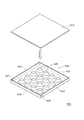
図1は、本実施の形態に係る照明装置の全体図である。
<First Embodiment>
Hereinafter, the lighting device according to the first embodiment of the present invention, the LED module and the LED mounting module used in the lighting device, and the LED mounting module manufacturing method will be described with reference to the drawings. While explaining.
(1) About lighting device Overall Structure FIG. 1 is an overall view of a lighting device according to the present embodiment.
照明装置10は、LED素子を実装するLEDモジュール100と、このLEDモジュール100を固定する固定部20と、LEDモジュール100から発せられた光を前方に反射する反射傘30と、固定部20のLEDモジュール100を保持する側と反対側に取着されたケース40と、このケース40の固定部20と反対側に取着された口金50と、ケース40の内部に収納され且つLEDモジュール100を点灯させる点灯ユニット(図示省略)とを備える。
The
ここで、口金50は、一般電球でも用いられているE型の口金、例えば、E26である。反射傘30は、LEDモジュール100から発せられた光を前方に反射させるためのものである。このため、反射傘30の内面には、例えば、白色塗料が塗布されていたり、反射傘30が金属の場合には鏡面状に仕上げられたりしている。
点灯ユニットは、商業電源を利用してLED素子を発光させる公知の回路が用いられており、例えば、商業電源から供給された交流電力を直流電力に整流する整流回路、この整流回路により整流された直流電力の電圧値を調整する電圧調整回路等を備える。
Here, the
As the lighting unit, a known circuit that emits LED elements using a commercial power source is used. For example, a rectifying circuit that rectifies AC power supplied from a commercial power source into DC power, and is rectified by the rectifying circuit. A voltage adjustment circuit for adjusting the voltage value of the DC power is provided.
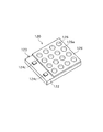
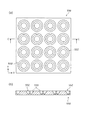
2.LEDモジュール
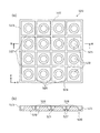
図2は、本実施の形態におけるLEDモジュールの斜視図であり、図3の(a)はLEDモジュールのLED素子が実装されている部分の拡大断面図であり、(b)はレンズ板を装着していない状態の拡大平面図である。
LEDモジュール100は、複数のLED素子110と、これらのLED素子110を表面に実装するためのLED実装用モジュール120と、LED実装用モジュール120の表面に設けられたレンズ板130とを備える。このLEDモジュール100は、LED素子110が直交する方向に規則正しく(ここでは、図2に示すように、直交する2方向に等間隔をおいて4行4列状態に)配された多点光源であり、これらのLED素子110を発光させることで面状光源として用いられる。
2. LED Module FIG. 2 is a perspective view of the LED module in the present embodiment, FIG. 3A is an enlarged cross-sectional view of a portion where the LED element of the LED module is mounted, and FIG. 2B is a lens plate. It is an enlarged plan view of a state where is not attached.
The
LED実装用モジュール120はLED素子110が実装されていないものを指し、逆に、LEDモジュール100はLED素子110が実装されているものを指す。
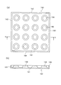
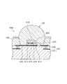
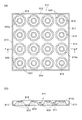
図4は、本実施の形態におけるLED実装用モジュールの斜視図であり、図5の(a)はLED実装用モジュールのLED素子が実装されている部分の拡大断面図であり、(b)はLED実装用モジュールのLED素子が実装されている部分の拡大平面図である。
The
FIG. 4 is a perspective view of the LED mounting module in the present embodiment, FIG. 5A is an enlarged cross-sectional view of a portion where the LED element of the LED mounting module is mounted, and FIG. It is an enlarged plan view of the part where the LED element of the module for LED mounting is mounted.
このLED実装用モジュール120は、図3〜図5に示すように、絶縁性の絶縁板122にLED素子110を実装するための配線パターン124が主面に形成されたプリント基板(本発明の「基板」に相当する。)123と、このプリント基板123の表面のLED素子の実装位置に対応して開設された反射孔126aを有する反射板(本発明の「反射体」に相当する。)126とを備える。ここで、反射板126は樹脂製であり、この反射板126とプリント基板123とは、対向する主面同士が直接接合された構造をしている。
As shown in FIGS. 3 to 5, the
絶縁板122は、例えば、セラミック材料を用いて形成されており、また、少なくとも、Al2O3、AlN、SiO2、SiCの一種以上を含んでいる。ここでは、例えば、Al2O3を含んでいる。
なお、Al2O3、AlN、SiO2、SiCの一種以上を含むことにより、絶縁板122の熱伝導率が向上するという効果が得られる。特に、LED素子は、発光時に熱も発生するので、絶縁板に熱伝導率の高い材料を使用することは、放熱特性の観点からも好ましい。
The insulating
By including one or more of Al 2 O 3 , AlN, SiO 2 , and SiC, the effect of improving the thermal conductivity of the insulating
配線パターン124は、絶縁板122の表面に形成され且つLED素子110と接続するパターン(以下、「表面パターン」という。)124aと、絶縁板122の内部に形成されているパターン(以下、「内部パターン」という。)124bと、絶縁板122の表面に形成された給電端子用のパターン(以下、「端子パターン」という)124cとを備える。
The
なお、表面パターン124aと内部パターン124bとは、ビアホール152bを介して接続され、また端子パターン124cと内部パターン124bとは、ビアホール(図示省略)を介して接続されている。
また、配線パターン124を絶縁板122の表面と内部とに分けて形成すると、例えば、絶縁板122の表面において表面パターン124aを形成する面積を少なくできるので、それだけ高密度でLED素子を実装できる。また、配線パターンの設計自由度が増すなどの効果も得られる。
The
Further, if the
反射板126の反射孔126aは、図3に示すように、プリント基板123側から当該プリント基板123と反対側(上側)に向かって、例えば、徐々に広がるテーパー状(所謂、上広がり状)に形成されている。この反射板126は、熱硬化性樹脂材料、具体的には、エポキシ樹脂により形成されており、内部にフィラーが混入されている。このフィラーは、少なくとも、TiO2、SiO2、Al2O3、BaSO4の一種以上混入されている。
As shown in FIG. 3, the
ここでは、例えば、TiO2を含んでいる。このように、TiO2、SiO2、Al2O3、BaSO4の一種以上を含むことにより、反射板の光の反射特性を向上させることができるという効果が得られる。なお、反射板の反射特性を向上させるために、例えば、反射孔を構成する壁面(テーパ-部分であり、反射面ともいう。)に蒸着、メッキ、その他の製法により金属薄膜を形成するようにしても良い。この場合、反射板内のTiO2等の混入物の有無は関係なくなる。 Here, for example, TiO 2 is included. As described above, by including one or more of TiO 2 , SiO 2 , Al 2 O 3 , and BaSO 4 , the effect that the light reflection characteristics of the reflector can be improved is obtained. In order to improve the reflection characteristics of the reflector, for example, a metal thin film is formed by vapor deposition, plating, or other manufacturing method on a wall surface (a taper portion, also referred to as a reflection surface) constituting the reflection hole. May be. In this case, the presence or absence of contaminants such as TiO 2 in the reflector is irrelevant.
ここで、前記蒸着について簡単に説明すると、反射板の反射孔内に露出している配線パターンをマスキングし、減圧雰囲気中で、例えば、Ag、Au、Alなどの反射率の高い金属材料の蒸着を行う。また、上記のその他の製法としては、例えば、ペースト状のAg、Au、Alなどの金属を反射面に塗布し、加熱してペーストの硬化を行う方法がある。
LED素子110には、図3に示すように、ここでは、裏面に両電極を有する裏面両電極型が用いられており、両電極が金バンプ111,112を介して配線パターン124aに接続されることで、LED素子110がプリント基板123に実装(フリップチップ実装)される。
Here, the vapor deposition will be briefly described. Masking the wiring pattern exposed in the reflection hole of the reflection plate, vapor deposition of a metal material having a high reflectance such as Ag, Au, Al, etc. in a reduced pressure atmosphere. I do. Moreover, as said other manufacturing method, there exists the method of apply | coating paste-like metals, such as Ag, Au, and Al, to a reflective surface, and heating and hardening a paste, for example.
As shown in FIG. 3, the
LED素子110から発せられた光を所望の光色に変換する必要がある場合、シリコーン又はエポキシ樹脂に所定の蛍光粉末を混入し、LED素子110を内包するように蛍光体140を形成すれば良い。
レンズ板130は、例えば、透光性を有するエポキシ樹脂により形成されており、図3に示すように、反射板126の反射孔126a、つまりLED素子110の実装位置に対応した部分が半球状に突出する凸レンズ130aとなっている。なお、反射板126の反射孔126a内にはレンズ板130を構成する樹脂材料が充填されており、凸レンズ130aと一体となっている。
When it is necessary to convert light emitted from the
The
ここで、反射板126及びレンズ板130の全体の平面視形状は、例えば、略正方形をしており、絶縁板122の平面視の形状は、反射板126及びレンズ板130の一辺を短辺とする長方形をしている。絶縁板122の表面であって、反射板126及びレンズ板130が配されていない面には、端子パターン124cが形成されている。
3.LEDモジュールの製造方法
上記構成のLEDモジュールの製造方法は、プリント基板を形成するプリント基板形成工程と、反射板を予め半硬化状態(本発明のBステージ状態に相当する。)に形成しておく(この状態のものを、「半硬化反射板」という。)半硬化反射板成形工程と、成形された半硬化反射板をプリント基板の表面に接合してLED実装用モジュールを形成するLED実装用モジュール形成工程と、LED実装用モジュールにLED素子を実装するLED実装工程と、実装されたLED素子を内包する蛍光体を成形する蛍光体成形工程と、レンズ板を成形するレンズ板成形工程とを含んでいる。
Here, the overall planar shape of the reflecting
3. Manufacturing method of LED module The manufacturing method of the LED module of the said structure forms the printed circuit board formation process and the reflecting plate in a semi-hardened state (equivalent to the B stage state of this invention) previously. (This state is referred to as a “semi-cured reflector”.) For LED mounting, a semi-cured reflector molding step and the molded semi-cured reflector are joined to the surface of the printed circuit board to form an LED mounting module. A module forming step, an LED mounting step of mounting an LED element on the LED mounting module, a phosphor molding step of molding a phosphor containing the mounted LED element, and a lens plate molding step of molding a lens plate Contains.
A.プリント基板形成工程
図6は、プリント基板形成工程を説明するための図である。
ここでは、プリント基板123を構成する絶縁板122として、Al2O3を含むセラミック材料を用いて形成する場合について説明する。
先ず、Al2O3を含むセラミック材料からなるグリーンシート151を準備(図6の(a))し、このグリーンシート151の表面に、例えば、タングステン、銅等の導電性ペーストを用いて内部パターン124b用のパターン153を、例えば、スクリーン印刷により形成する。
A. Printed Circuit Board Forming Process FIG. 6 is a diagram for explaining the printed circuit board forming process.
Here, the case where the insulating
First, a
上記グリーンシート151とは別のグリーンシート152を準備し、このグリーンシート152の所定位置に、例えば、打ち抜き加工等により貫通孔を形成する。そして、形成された貫通孔に、例えば、タングステン、銅等の導電性ペーストを充填して、ビアホール152a,152aを形成する(図6の(c))。
そして、このビアホール152a,152aを備えるグリーンシート152を、もう一方のグリーンシート151の表面(パターン153が形成されている面)に積層して圧着する(図6の(d))。このようにして積層された表側のグリーンシート152の表面に表面パターン124a用のパターン154,154を、例えば、タングステン、銅等の導電性ペーストを用いてスクリーン印刷する(図6の(e))。
A
Then, the
最後に、積層されたグリーンシート151,152を所定温度で焼成して、パターン154,154上にニッケル、金等でメッキ等を行い、絶縁板122に配線パターン124が形成されたプリント基板123が完成する(図6の(f))。
なお、本工程において表面パターン124aは、パターン154,154を印刷によって行っているが、例えば、スパッタリング、蒸着、メッキ等により形成しても良い。また、セラミック材料の焼成温度に合わせて、導電性ペーストとして、銀等を用いて良い。
Finally, the laminated
In this step, the
B.半硬化反射板成形工程
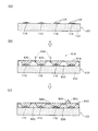
図7は、半硬化反射板の成形に用いる成形金型を示し、(a)は平面図であり、(b)は図7の(a)のAA線における断面を矢印方向から見た図である。
成形金型160は、上面が開口する箱状をしており、平面視形状は反射板126に対応してほぼ正方形をしている。この成形金型160は、底壁161と、この底壁161の各端縁から立設する側壁162,163,164,165とを備えると共に、底壁161の内面から截頭円錐状に突出する突出部166が4行4列のマトリックス状に形成されている。なお、この成形金型160で成形すると、突出部166の部分が、反射板126の反射孔126aに相当する。
B. FIG. 7 shows a molding die used for molding the semi-cured reflector, (a) is a plan view, and (b) is a cross-sectional view taken along line AA in FIG. It is the figure seen from the direction.
The molding die 160 has a box shape with an upper surface opened, and the shape in plan view is substantially square corresponding to the
図8は、半硬化反射板成形工程を説明するための図である。
まず、上記構成の成形金型160の開口が上となるように、且つ底壁161が略水平となるように成形金型160を設置する。そして、液体状の、例えば、エポキシ樹脂167を成形金型160内に充填させた(図8の(a))後、充填させたエポキシ樹脂167の内、余分なエポキシ樹脂167を除去する。
FIG. 8 is a diagram for explaining the semi-cured reflector forming step.
First, the molding die 160 is installed so that the opening of the molding die 160 having the above configuration is on the top and the
この樹脂材料(167)は、主成分をエポキシ樹脂とし、この樹脂材料内に、反射効率を高めるためのTiO2が含まれている。
上記余分なエポキシ樹脂167の除去は、例えば、スキージ168を用い、その一辺を成形金型160の上縁に当てて、例えば、図8の(b)に示すように、矢印方向に移動させることで行う。
This resin material (167) is mainly composed of an epoxy resin, and TiO 2 for increasing the reflection efficiency is contained in the resin material.
The excess
次に、充填したエポキシ樹脂167を加熱して半硬化状態にする。これにより半硬化反射板167aの成形が完了する。なお、エポキシ樹脂167の加熱条件は、例えば、80℃で15分である。この加熱条件は、エポキシ樹脂167の種類によって変わるものであり、使用する樹脂材料に合せて適宜決定する必要がある。
C.LED実装用モジュール形成工程
図9は、LED実装用モジュール形成工程を説明する図である。
Next, the filled
C. LED Mounting Module Forming Process FIG. 9 is a diagram for explaining the LED mounting module forming process.
まず、上記プリント基板形成工程で形成されたプリント基板123と、半硬化反射板成形工程で成形された半硬化反射板167aとを準備して、プリント基板123におけるLED素子110の実装位置が半硬化反射板167aの孔167bの略中央になるように、半硬化反射板167aをプリント基板123の配線パターン124がある面に載置する(図9の(a))。
First, the printed
この際、半硬化反射板167aは、半硬化状態、いわゆるBステージの状態であるため、自己の形状を保持しているので、その取扱いが容易であり、載置作業が効率良く行える。
次に、プリント基板123上に載置した半硬化反射板167aに対して加圧部材169を用いて加圧し、この状態を保持しつつ加熱して半硬化反射板167aを硬化させる。このとき、半硬化反射板167aは、Bステージ状態であるため、加熱により半硬化反射板167aを構成している樹脂材料の粘度が低下し、半硬化反射板167aがプリント基板123に密着した状態で半硬化反射板167aの樹脂材料が硬化する。これにより、プリント基板123と反射板126とが、対向する面同士で直接接合されたことになると共に、LED実装用モジュール120が完成する(図9の(c))。
At this time, since the
Next, the semi-cured
また、プリント基板123の表面に半硬化反射板167aを載置した状態で両者の面同士間に、例えば、配線パターン124の凹凸等による隙間があっても、半硬化反射板167aの樹脂材料は加熱により粘度が低下するため、前記隙間に樹脂材料が流れ込み、確実にプリント基板123と反射板126とを密着した状態で接合できる。このため、反射板126とプリント基板123との面同士に隙間がなくなり、LED素子110から発せられた光を吸収することなく所定方向に効率良く反射させることができる。
In addition, even if there is a gap due to the unevenness of the
さらに、例えば、反射板とプリント基板とを接着層で固着する場合には、反射板をプリント基板に載置する前に、接着シート等をプリント基板上に配置する必要があり、この載置する際に、接着シートが非常に薄くその扱いが困難であったが、本発明では、反射板126の形状を保持した半硬化反射板167aを用いているため、半硬化反射板167aの載置が容易且つ効率良く行える。
Furthermore, for example, when the reflecting plate and the printed board are fixed with an adhesive layer, it is necessary to place an adhesive sheet or the like on the printed board before placing the reflecting board on the printed board. At this time, the adhesive sheet is very thin and difficult to handle. However, in the present invention, since the
D.LED実装工程
図10は、LED実装工程を説明するための図である。
まず、LED実装用モジュール120のLED素子の実装位置に、例えば、金バンプ111,112を形成する(図10の(a))。なお、LED素子の実装位置は、配線パターン124上にあるのは言うまでもない。
D. LED Mounting Process FIG. 10 is a diagram for explaining the LED mounting process.
First, for example, gold bumps 111 and 112 are formed at the LED element mounting position of the LED mounting module 120 (FIG. 10A). Needless to say, the mounting position of the LED element is on the
次に、LED素子110をLED実装用モジュール120の実装位置に形成された金バンプ111,112上に載置する。具体的には、LED素子110を吸引保持するコレット170を用いている(図10の(b))。このコレット170にLED素子110を吸着させた状態で、LED素子110を金バンプ111,112上に配置する。そして、この吸引保持した状態で、LED素子110を加熱すると共に高周波(超音波)振動させる。これにより金バンプ111,112が溶融した後固化することで、LED素子110が金バンプ111,112を介して表面パターン124aに実装される。
Next, the
なお、本明細書では、LEDモジュールは、レンズ板130等を備えたものとしているため、LED実装用モジュール120にLED素子110を実装したものを、LED実装モジュールとして他のモジュールと区別する。
E.蛍光体成形工程
図11は、蛍光体成形工程を説明するための図である。
In the present specification, since the LED module includes the
E. Phosphor Forming Process FIG. 11 is a diagram for explaining the phosphor forming process.
上記LED実装工程で、LED素子110が実装されたLED実装モジュールに対して、蛍光体140を成形する成形冶具171をセットする。この成形冶具171は、略板状をしており、反射板126の反射孔126aに対応する部分が、反射孔126a内に突出する突出部171bとなっており、この中央に貫通孔171aが成形されている。また突出部171bの先端側の端縁はプリント基板123の表面に当接するようになっている。
In the LED mounting step, a forming
そして、LED実装モジュールに成形冶具171を覆設した状態で、蛍光体140に用いられる液状(硬化前の状態)の樹脂材料に所定の蛍光粉末を混入させて、蛍光粉末入りの樹脂材料172を成形冶具171の貫通孔171aに滴下させる(図11の(a))。なお、滴下する樹脂材料172の量は、蛍光体140の大きさに対応する量である。
全ての成形冶具171の貫通孔171aに、樹脂材料172の滴下が完了すると(図11の(b))、樹脂材料を加熱して硬化させる。なお、樹脂材料の硬化条件は、例えば、150℃、30分であるが、これに限定するものではなく、種々の硬化条件を採用することもできる。
Then, in a state where the
When dripping of the
樹脂材料の硬化が完了すると、成形冶具171をLED実装モジュールから取り外す。
F.レンズ板成形工程
図12は、レンズ板成形工程を説明するための図である。
上記蛍光体成形工程で蛍光体140が成形されたLED実装モジュールに対して、レンズ板130を成形する成形冶具173をセットする。この成形冶具173は、略板状をしており、反射板126の反射孔126aに対応する部分が、内方に凹入する凹入部174が設けられている。また、隣接する凹入部174間は、反射板126の表面と所定寸法(レンズ板130の厚さに相当する)離れている。
When the curing of the resin material is completed, the
F. Lens Plate Molding Step FIG. 12 is a diagram for explaining the lens plate molding step.
A
そして、LED実装モジュールに成形冶具173を覆設した状態で、レンズ板130に用いられる液状(硬化前の状態)の樹脂材料を成形冶具173内に注入させる(図12の(a))。
成形冶具173内に樹脂材料の注入が完了すると、注入した樹脂材料を加熱して硬化させる。なお、樹脂材料の成形条件は、例えば、150℃、10分であるが、これに限定するものではなく、種々の硬化条件を採用することもできる。
Then, in a state where the
When the injection of the resin material into the forming
樹脂材料の硬化が完了すると、成形冶具173から取り外して、LEDモジュール100の製作が完了する(図12の(b))。
4.その他
本発明は、上記2.LEDモジュールの欄で説明した構成に限定するものではない。
つまり、上記説明は、LED素子のタイプ(接続方法)、絶縁板の構造、蛍光体の有無、蛍光体の形状及び成形方法、反射板の成形方法等を示す一例であり、以下のような変形例を実施できる。以下、第1の実施の形態を基にした変形例1から変形例4について、図13及び図14を用いて説明する。
When the curing of the resin material is completed, it is removed from the forming
4). Others The present invention provides the above-mentioned 2. The configuration is not limited to that described in the LED module column.
That is, the above description is an example showing the type (connection method) of the LED element, the structure of the insulating plate, the presence / absence of the phosphor, the shape and molding method of the phosphor, the molding method of the reflecting plate, etc. An example can be implemented. Hereinafter, Modification 1 to Modification 4 based on the first embodiment will be described with reference to FIGS. 13 and 14.
図13の(a)は、変形例1のLEDモジュールの断面図であり、図13の(b)は、変形例2のLEDモジュールの断面図である。なお、図13の(a)及び(b)では、第1の実施の形態と同じ構成のものは、そのまま同じ符号を用いて表している。
図13の(a)に示す変形例1は、LED素子110を内包する蛍光体を備えていないLEDモジュール200を示している。
FIG. 13A is a cross-sectional view of the LED module of the first modification, and FIG. 13B is a cross-sectional view of the LED module of the second modification. In FIGS. 13A and 13B, the same components as those in the first embodiment are denoted by the same reference numerals as they are.
Modification 1 shown in FIG. 13A shows an
この場合、LED素子110から発せられた光を所定の光色に変換する必要があるときは、レンズ板202を構成する樹脂材料に所定の蛍光粉末を混入したり、レンズ板202の外周面に蛍光粉末を含浸する液体を塗布して蛍光層を形成したりすることで実施できる。
なお、このようなLEDモジュール200でも、上述したLEDモジュール100の製造方法を基本的に利用すれば、実現できると共に、反射板126とプリント基板123との主面同士を直接接合できる。
In this case, when it is necessary to convert the light emitted from the
In addition, such an
図13の(b)に示す変形例2は、LED素子として、表面に2つの電極を有する表面両電極型のLED素子222を用い、また、LED素子222を内包する蛍光体224を、成形冶具を用いずに成形した場合のLEDモジュール220を示している。
LED素子222は、表面両電極型を用いたため、絶縁板122の表面に成形されている配線パターン226に金線228,230を用いて接続されている。次に、蛍光体224は、所定の蛍光粉末を含んだ液状の樹脂材料を滴下して成形している。つまり、硬化前の粘度の高い樹脂材料を用いることで、滴下した状態を略保持することを利用して、そのまま硬化したものである。
In Modification 2 shown in FIG. 13B, a surface-both electrode
Since the
図13の(b)では、配線パターン226の一方が、LED素子222全体を搭載できるように成形されており、LED素子222は、例えば、絶縁性又は導電性の接着剤、銀ペースト等を利用して配線パターン226に接合されている。なお、配線パターンを、図13の(b)のようにLED素子222を搭載できる大きさに成形せずに、LED素子を絶縁板122に接着剤等を介して直接取り付けるようにしても良い。
In FIG. 13B, one of the
変形例2におけるLEDモジュール220も、上述したLEDモジュール100の製造方法における蛍光体成形工程をここで説明した内容の工程に替えるだけで実現できる。なお、ここでも、反射板126とプリント基板232との面同士が直接接合されている。
図14の(a)は、変形例3のLEDモジュールの断面図であり、図14の(b)は、変形例4のLEDモジュールの断面図である。なお、図14の(a)及び(b)でも、第1の実施の形態と同じ構成のものは、そのまま同じ符号を用いて表している。
The
FIG. 14A is a cross-sectional view of the LED module of Modification Example 3, and FIG. 14B is a cross-sectional view of the LED module of Modification Example 4. 14A and 14B, the same components as those in the first embodiment are denoted by the same reference numerals as they are.
図14の(a)に示す変形例3は、絶縁板252の表面にだけ配線パターンを有したLEDモジュール250を示し、図14の(b)に示す変形例4も同じく、絶縁板272の表面にだけ配線パターンを有したLEDモジュール270を示す。
上記実施の形態では、絶縁板122は、図6に示したように、2層のグリーンシート151,152を用い、両グリーンシート151,152の間にパターン153を備え、ビアホール152bを介して表面パターン124aに接続する構造を採用しているが、この構造に限定するものでなく、図14の(a)の変形例3のような、絶縁板252と、この絶縁板252の表面にのみ形成された配線パターン254とからプリント基板256を構成しても良し、図14の(b)の変形例4のような、絶縁板272と、この絶縁板272の表面にのみ形成された配線パターン274とからプリント基板276を構成しても良い。
Modification 3 shown in FIG. 14A shows an
In the above embodiment, as shown in FIG. 6, the insulating
<第2の実施の形態>
以下、本発明の第2の実施の形態に係るLEDモジュールについて図面を参照しながら説明する。
第2の実施の形態は、基板の裏面に金属板が積層され、絶縁板が無機フィラーと熱硬化性樹脂材料とを含むコンポジット材料で成形している点で、第1の実施の形態と異なる。
<Second Embodiment>
Hereinafter, an LED module according to a second embodiment of the present invention will be described with reference to the drawings.
The second embodiment is different from the first embodiment in that a metal plate is laminated on the back surface of the substrate, and the insulating plate is formed of a composite material including an inorganic filler and a thermosetting resin material. .
(1)LEDモジュールの構成について
図15は、第2の実施の形態におけるLEDモジュールの断面概略図である。
まず、第2の実施の形態におけるLEDモジュール300は、LED素子310と、このLED素子310を実装するためのLED実装用モジュール320と、実装されているLED素子310を内包する蛍光体340と、LED実装用モジュール320の表面に設けられたレンズ板330とを備える。
(1) Configuration of LED Module FIG. 15 is a schematic cross-sectional view of an LED module according to the second embodiment.
First, an
LED実装用モジュール320は、プリント基板320aと、樹脂製の反射板326と、前記プリント基板320aの裏面に装着された金属板350とを備え、プリント基板320aは、Al2O3(アルミナ)フィラー及びエポキシ樹脂を含むコンポジット材料からなる絶縁板323と、表面にLED素子310を実装するための配線パターンとからなる。
The
絶縁板323は、単数又は複数、ここでは2層の絶縁層からなり、表面側の絶縁層を上部絶縁層321と、また裏面側の絶縁層を下部絶縁層322とする。各絶縁層321,322の表面には、配線用のパターン324,325が成形されており、両者は、ビアホール327,327を介して接続されている。
また、各絶縁層321,322のパターンを区別するために、下部絶縁層322に形成されているパターンを内部パターン325と、上部絶縁層321に形成されているパターンを表面パターン324とそれぞれする。
The insulating
Further, in order to distinguish the patterns of the insulating
LED素子310は、第1の実施の形態と同様に、金バンプ328,329を介して表面パターン324に実装される。蛍光体340、レンズ板330については、第1の実施の形態と同じであり、また同じ方法で成形される。
本実施の形態においても、反射板326は、半硬化状態でプリント基板320aの表面に載置され、加熱圧縮される。これにより、反射板326及びプリント基板320aとが直接接合されることになる。
The
Also in the present embodiment, the
(2)製造方法について
次に、本実施の形態におけるプリント基板320aの成形方法について説明する。
図16は、金属板350が貼着されたプリント基板320aの形成工程を説明する図である。
まず、一の主面(表面)に銅箔366を有するプリプレグと、アルミニウム製の金属板362とを準備する。前記プリプレグは、アルミナフィラーとエポキシ樹脂(未硬化)とからなり、基板形成後は下部絶縁層322に相当する。このプリプレグの裏面が金属板362側となるようにプリプレグを前記金属板362に貼り付け、加熱・加圧を行い、プリプレグの(完全)硬化を行うと共に金属板362と接合する(図16の(a))。
(2) Manufacturing Method Next, a method for forming the printed
FIG. 16 is a diagram illustrating a process of forming the printed
First, a prepreg having a
金属板362付きの絶縁板364の表面に貼着されている銅箔366に内部パターン325に相当するパターン366aを形成する(図16の(b))。この形成には、例えば、フォトリソグラフィ法が用いられ、銅箔366の表面にドライフィルム(感光レジストをフィルム状にしたもの)と、内部パターン325用のパターンが形成された露光フィルム(マスクフィルム)とをこの順で銅箔に貼り付け、例えば、紫外線等を照射させてドライフィルムの現像を行い、この現像されたパターンに基づいて銅箔をエッチングした後、ドライフィルムを除去することで行われる。
A
内部パターン325用のパターン366aが形成されると、上部絶縁層321に相当するプリプレグ(表面に銅箔369を有する)を表側(外側)として絶縁板364のパターン366a側の面に貼り付けて、加熱・加圧してプリプレグを硬化すると共に絶縁板368とすでに形成されている絶縁板364とを接合する(図16の(c))。
次に、プリント基板320aにおけるビアホール327の位置にある銅箔369bの一部を、例えば、上記フォトリソグラフィ法を利用してエッチングにより除去し、その部分にスルーホール371を形成する(図16の(d))。スルーホール371の形成には、例えば、CO2レーザを用いている。
When the
Next, a part of the copper foil 369b at the position of the via
スルーホール371が形成されると、スルーホール371の内部及び銅箔369の表面に銅メッキを行い、ビアホール375を形成する(図16の(e))。なお、前記スルーホール371の内部に、例えば、タングステン、銅、銀等の導電性ペーストを充填し、その後、銅箔の表面に銅メッキを行っても良い。ここで、銅箔369上に銅メッキされたものを銅層379とする。
When the through
最後に、銅層379に表面パターン324に相当するパターンを形成して、金属板350が貼着されたプリント基板320aが完成する。なお、表面パターン324の形成は、例えば、内部パターン325と同様に、フォトリソグラフィ法を利用して行っている。
なお、表面パターン324は、銅層379をパターンニングした後に、例えば、ニッケル、金メッキを施している。これは、最後にめっき加工した方が、バンプの材料である金との接合、配線パターンの耐食性の向上が図れるからである。
Finally, a pattern corresponding to the
The
(3)その他
本発明に係るLED実装用モジュール、LEDモジュールは、上記構成に限定するものではない。
つまり、上記説明は、LED素子のタイプ(接続方法)、絶縁板の構造、蛍光体の有無、蛍光体の形状及び成形方法、反射板の成形方法等を示す一例であり、第1の実施の形態の(4)その他の欄で説明したような構成でも実施できる。
(3) Others The LED mounting module and the LED module according to the present invention are not limited to the above configuration.
That is, the above description is an example showing the type of LED element (connection method), the structure of the insulating plate, the presence / absence of the phosphor, the shape and molding method of the phosphor, the molding method of the reflector, and the like. The configuration as described in (4) Other column of the embodiment can also be implemented.
当然、LED素子の個数、その配列・配置も上記の説明に限定するものではない。例えば、LED素子は、上記説明では、4行4列に配列されていたが、N行M列(N、Mは整数であり、NとMは同じ整数でも良いし、異なった整数でも良い。)で配置しても良い。さらには、平面視において、複数のLED素子を菱形状、三角形状等の多角形状、楕円(円形も含む)形状に配置しても良い。 Of course, the number of LED elements and their arrangement / arrangement are not limited to the above description. For example, the LED elements are arranged in 4 rows and 4 columns in the above description, but N rows and M columns (N and M are integers, and N and M may be the same integer or different integers. ). Furthermore, in plan view, the plurality of LED elements may be arranged in a polygonal shape such as a rhombus shape or a triangular shape, or an elliptical shape (including a circular shape).
また、第2の実施の形態では、絶縁板323は、図15及び図16に示したように、アルミナフィラーとエポキシ樹脂からなるコンポジット層を2層(321,322)用い、各層に接続用のパターン324,325を有しているが、この構造に限定するものでなく、以下、第2の実施の形態に基づいた変形例5及び6について図17を用いて説明する。
図17の(a)は、変形例5のLEDモジュールの断面図であり、図17の(b)は、変形例6のLEDモジュールの断面図である。なお、図17の(a)及び(b)では、第2の実施の形態と同じ構成のものは、そのまま同じ符号を用いて表している。
In the second embodiment, as shown in FIGS. 15 and 16, the insulating
FIG. 17A is a cross-sectional view of the LED module of Modification Example 5, and FIG. 17B is a cross-sectional view of the LED module of Modification Example 6. In FIGS. 17A and 17B, the same components as those of the second embodiment are represented by the same reference numerals as they are.
変形例5におけるLEDモジュール370は、図17の(a)に示すように、アルミナフィラーとエポキシ樹脂からなるコンポジット層を1層用いた絶縁板372と、この絶縁板372の表面の配線パターン374とからなるプリント基板376を備える。なお、コンポジット層を1層用いた絶縁板372は、図16の(b)と同様に、配線パターン374用のパターンが形成された絶縁板372を用いて、最後にパターンにメッキ加工を施すことにより実施できる。
As shown in FIG. 17A, the
変形例6におけるLEDモジュール380は、図17の(b)に示すように、変形例2で説明した表面両電極型のLED素子390を用い、また、変形例2で説明した方法で成形された蛍光体392を備えている。
なお、このような変形例6におけるLEDモジュール380も、変形例5で説明した方法でプリント基板384を成形した後、第1の実施の形態のLEDモジュール100の製造方法における蛍光体成形工程を変形例2で説明した方法を用いることにより実現できる。
As shown in FIG. 17B, the
Note that the
また、変形例5のLEDモジュール370及び変形例6のLEDモジュール380でも、反射板326とプリント基板376,384との面同士が直接接合されている。
なお、第2の実施の形態における絶縁板323は2層の絶縁層321,322から、また、変形例5及び6におけるプリント基板376,384は1層の絶縁板372からそれぞれ構成されているが、言うまでも無く、絶縁板は、3層以上の絶縁層から構成しても良い。
Also in the
The insulating
<第1及び第2の実施の形態について>
以上、本発明を上記の第1及び第2の実施の形態及び変形例1〜6に基づいて説明したが、本発明の内容が、上記各実施の形態及び各変形例に示された具体例に限定されないことは勿論であり、例えば、以下のような変形例をさらに実施することができる。なお、以下で説明する「第1及び第2の実施の形態等」には、第1及び第2の実施の形態の他、これらについての変形例である変形例1〜6も含んだ概念として使用する。
<About the first and second embodiments>
As mentioned above, although this invention was demonstrated based on said 1st and 2nd embodiment and the modifications 1-6, the content of this invention is the specific example shown by said each embodiment and each modification. Of course, the present invention is not limited to this, and for example, the following modifications can be further implemented. In addition, in the “first and second embodiments, etc.” to be described below, in addition to the first and second embodiments, the concept includes modifications 1 to 6 which are modifications thereof. use.
(1)反射板
1.成形方法
上記第1及び第2の実施の形態等における半硬化反射板は、成形金型に樹脂材料を充填させて硬化させているが、例えば、射出成形により半硬化状態に成形しても良く、以下、変形例7として説明する。
(1) Reflector 1. Molding Method The semi-cured reflector in the first and second embodiments is cured by filling a molding die with a resin material, but may be molded into a semi-cured state by, for example, injection molding. Hereinafter, this will be described as a modified example 7.
図18は、変形例7における半硬化反射板の成形に用いる成形金型の分解斜視図であり、図19は、(a)は、変形例7における成形金型の断面図であり、(b)は成形金型の上型を外した状態での平面図である。
成形金型400は、射出成形用であり、図18に示すように、例えば、第1の実施の形態で説明した成形金型160を下型420とし、この下型420の開口を塞ぐ上型410とを備え、反射板を形成するときに、上型410と下型420とを組合わせると、その内部に反射板を形成すべき成形空間ができる。なお、上型410と下型420とが組合された状態では、内部に注入された樹脂材料が外部に漏洩しないようになっている。
FIG. 18 is an exploded perspective view of a molding die used for molding the semi-cured reflecting plate in Modification 7. FIG. 19A is a sectional view of the molding die in Modification 7. ) Is a plan view with the upper mold of the molding die removed.
The molding die 400 is for injection molding. As shown in FIG. 18, for example, the molding die 160 described in the first embodiment is used as the
下型420は、第1の実施の形態と同様に、底壁421と、4つの側壁422,423,424,425を備える箱形状をしている。底壁421には反射孔用の突出部426が、側壁422には樹脂材料の注入口427が、また、側壁424には樹脂材料の注出口428がそれぞれ設けられている。
半硬化反射板を成形するには、液体状の樹脂材料を、上型410及び下型420を組合わせた状態で注入口427から注入し、注出口428から樹脂材料が注出するまで樹脂材料の注入を行い、この成形金型400内に樹脂材料が充填されると加熱して半硬化状態に成形すれば良い。
The
To mold the semi-cured reflector, a liquid resin material is injected from the
なお、射出成形により半硬化反射板を成形する際の成形条件は、第1の実施の形態の半硬化反射板成形工程で説明した条件と同じであり、このように射出成形により半硬化反射板を成形すると、寸法精度の良い成形物が効率良く得られる。このため、半硬化反射板をプリント基板に接合する際に、半硬化反射板をプリント基板に載置したときに、プリント基板の主面に対する半硬化反射板の傾きが少なく、加圧部材(169)で半硬化反射板の上面を均等に加圧できる。これにより、厚みムラの少ない反射板、ひいてはLED実装モジュールが得られる。 The molding conditions for molding the semi-cured reflector by injection molding are the same as those described in the semi-cured reflector molding step of the first embodiment, and thus the semi-cured reflector by injection molding. When molding is performed, a molded article with good dimensional accuracy can be obtained efficiently. For this reason, when the semi-cured reflective plate is bonded to the printed circuit board, when the semi-cured reflective plate is placed on the printed circuit board, the semi-cured reflective plate is less inclined with respect to the main surface of the printed circuit board. ) Can uniformly pressurize the upper surface of the semi-cured reflector. Thereby, a reflector with little thickness unevenness, and an LED mounting module can be obtained.
2.構成について
上記第1及び第2の実施の形態等では、反射板は、LED素子の実装位置に対応して、独立した16個の反射孔を有した1枚の板状をしているが、この構成に限定されるものではない。つまり、LED素子に対応して別個独立に反射体を準備し、各反射体を独立形態でプリント基板に接合しても良い。
2. Regarding the configuration In the first and second embodiments and the like, the reflecting plate has a single plate shape with 16 independent reflecting holes corresponding to the mounting positions of the LED elements. It is not limited to this configuration. In other words, reflectors may be prepared separately and correspondingly to the LED elements, and each reflector may be bonded to the printed board in an independent form.
以下、反射板の構成を変形させた変形例8及び9を図20、図21及び図22、図23を用いて説明する。
図20は、変形例8におけるLED実装用モジュールの斜視図である。
変形例8におけるLED実装用モジュール510は、図20に示すように、配線パターンを備える(図示省略)プリント基板512と、このプリント基板512の表面に設けられた複数(16)個の反射体514とからなる。
Hereinafter, modified examples 8 and 9 in which the configuration of the reflecting plate is modified will be described with reference to FIGS. 20, 21, 22, and 23.
FIG. 20 is a perspective view of an LED mounting module according to Modification 8.
As shown in FIG. 20, the
反射体514は、図20からも明らかなように、その中央部に反射孔516を有している。つまり、1つの反射体514は、1つの反射孔516を備えている。なお、この反射孔516は、第1及び第2の実施の形態等と同様に、反射体514の表面側からプリント基板512側に近づくに従って先細りする形状になっている。反射体514のプリント基板512への取着は、第1の実施の形態と同様に、半硬化状態の反射体514を、プリント基板512上の所定位置にセットし、表側から加圧しながら加熱して反射体514を硬化することで行う。
As is clear from FIG. 20, the
図21の(a)は、変形例8における反射体を成形するための成形金型の平面図であり、図21の(b)は、図21の(a)のB−B線における断面を矢印方向から見た図である。
成形金型520は、図21に示すように、第1の実施の形態における反射板126用の成形金型160と同様に、底壁521と、4つの側壁522,523,524,525とを備える箱状をしている。
FIG. 21A is a plan view of a molding die for molding the reflector in the modified example 8, and FIG. 21B is a cross-sectional view taken along the line BB in FIG. It is the figure seen from the arrow direction.
As shown in FIG. 21, the molding die 520 includes a
箱状の成形金型520の内部は、側壁522,523,524,525と、縦横方向(図中のXY方向)の縦壁526及び横壁527とにより縦横計16個に区画されている。区画されている部分の各底壁521は、その略中央部に反射体514の反射孔516を成形するための突出部528を備えている。なお、突出部528は、反射孔516の形状に合せて、基部側から先端側に移るに従って細くなっている。
The inside of the box-shaped molding die 520 is divided into 16 vertical and horizontal totals by
なお、成形金型520は、一度の成形で16個の反射体514が得られるように、その内部が16個に区画されているが、例えば、成形金型は1個の区画に相当する部分を有し、一度の成形で1個の反射体が得られるような構成にしても良い。
図22は、変形例9におけるLED実装用モジュールの斜視図である。
変形例9におけるLED実装用モジュール530も、変形例8と同様に、配線パターンを備える(図示省略)プリント基板532と、このプリント基板532の表面に設けられた複数(16)個の反射体534とからなる。
The molding die 520 is divided into 16 sections so that 16
FIG. 22 is a perspective view of an LED mounting module in Modification 9.
Similarly to Modification 8,
各反射体534は、図22からも明らかなように、その中央部に反射孔536を1つ有している。なお、この反射孔536は、反射体534の表面側からプリント基板532側に近づくに従って先細りする形状になっている。反射体534のプリント基板532への取着は、変形例8と同様である。
図23の(a)は、変形例9における反射体を成形するための成形金型の平面図であり、図23の(b)は、図23の(a)のC−C線における断面を矢印方向から見た図である。
Each
FIG. 23A is a plan view of a molding die for molding the reflector in the modified example 9, and FIG. 23B is a cross-sectional view taken along the line CC of FIG. It is the figure seen from the arrow direction.
成形金型550は、図23に示すように、板状をしており、縦横方向(図中のXY方向)に4個づつ並んだ計16の凹入部552を有している。この凹入部552は、平面視したとき、つまり、図23の(a)の状態では、リング状に凹入している。なお、凹入部552の内周側の側壁553の径は、反射孔536の形状に対応して成形金型550の表側(開口を有する側)から底側に移るに従って大きくなっている。
As shown in FIG. 23, the molding die 550 has a plate shape and has a total of 16 recessed
3.樹脂材料の種類について
第1及び第2の実施の形態等では、エポキシ樹脂を用いて反射板を成形しているが、他の樹脂材料、例えば、不飽和エステル樹脂、フェノール樹脂、ポリイミド樹脂、ポリフタルアミド樹脂等を用いても良い。
(2)最後に
第1及び第2の実施の形態等では、半硬化状態の反射体をプリント基板に貼り付けて完全硬化させているが、基板と反射体とを直接接触した状態で接合するという思想から見れば、例えば、プリント基板を樹脂材料で構成し、その樹脂材料が半硬化の状態で反射体(このときの反射板は半硬化・完全硬化を問わない)をプリント基板に重ねて、その後加熱・加圧により両者を接合させることも可能である。
3. Regarding types of resin materials In the first and second embodiments, etc., the reflecting plate is molded using an epoxy resin. However, other resin materials such as unsaturated ester resins, phenol resins, polyimide resins, poly A phthalamide resin or the like may be used.
(2) Finally, in the first and second embodiments, the semi-cured reflector is attached to the printed circuit board and completely cured, but the substrate and the reflector are joined in direct contact. For example, if the printed circuit board is made of a resin material and the resin material is semi-cured, a reflector (in this case, the reflecting plate may be semi-cured or completely cured) is stacked on the printed circuit board. Then, it is also possible to join both by heating and pressurization.
なお、プリント基板を半硬化状態で両者を接合すると、プリント基板の表面に形成されている配線パターンが波打つ、あるいはLED素子の実装位置が湾曲するなどの問題が発生する惧れがあるが、例えば、反射体の反射孔を利用して配線パターンのLED素子の実装位置(LED素子は、まだ実装されていない)を金型で成形時に押圧すれば、その部分の配線パターンを平坦状にできる。 If the printed circuit boards are joined together in a semi-cured state, the wiring pattern formed on the surface of the printed circuit board may be wavy or the mounting position of the LED element may be curved. If the mounting position of the LED element of the wiring pattern (the LED element is not yet mounted) is pressed at the time of molding with a mold using the reflection hole of the reflector, the wiring pattern of that portion can be made flat.
一方、第2の実施の形態では、反射体とプリント基板とを構成する樹脂材料に同種のもの(エポキシ樹脂)を用いたが、反射体とプリント基板との樹脂材料の種類が異なっていても良い。但し、反射体とプリント基板との接合力は、同種の樹脂材料を用いた方が強くなる可能性がある。
なお、上記第2の実施の形態では、プリント基板を構成するプリプレグの成形段階では、その樹脂材料を完全硬化させているが、例えば、プリント基板用の樹脂材料を、完全硬化の手前で加熱を止め、反射体との接合時にまとめて完全硬化(ポストキュア)させても良い。このようにプリント基板を形成すると、プリント基板形成時の時間短縮が可能となり、生産性の向上を図ることができる。
On the other hand, in the second embodiment, the same kind of resin material (epoxy resin) is used as the resin material constituting the reflector and the printed board, but the type of resin material between the reflector and the printed board is different. good. However, the bonding force between the reflector and the printed board may be stronger when the same kind of resin material is used.
In the second embodiment, the resin material is completely cured at the molding stage of the prepreg constituting the printed circuit board. For example, the resin material for the printed circuit board is heated before the complete curing. It may be completely cured (post cure) at the time of stopping and joining with the reflector. When the printed circuit board is formed in this way, the time required for forming the printed circuit board can be shortened, and the productivity can be improved.
さらには、上記第1及び第2の実施の形態では、LED素子をプリント基板に直接的に実装しているが、本発明では、LED素子をプリント基板に間接的に実装しても良い。この例を、LED素子をサブマウント方式でプリント基板に実装した変形例10で説明する。
図24は、LED素子を間接的に実装させた変形例10におけるLEDモジュールの断面図である。
Further, in the first and second embodiments, the LED element is directly mounted on the printed board. However, in the present invention, the LED element may be indirectly mounted on the printed board. This example will be described as a modified example 10 in which the LED element is mounted on the printed board by the submount method.
FIG. 24 is a cross-sectional view of the LED module in
変形例10におけるLEDモジュール600は、変形例2で説明したものと同じ構成のLED実装用モジュールが用いられている。LED実装用モジュールは、プリント基板232と反射板126とを備える。LED実装用モジュールのLED実装位置には、LED素子610がサブマウント605として間接的に実装されている。なお、LEDモジュール600は、変形例2と同様にレンズ板130を備えている。
As the
サブマウント605は、例えば、シリコン基板(以下、「Si基板」という。)612と、このSi基板612の上面に実装されたLED素子610と、LED素子610を内包する蛍光体618とを備える。ここでは、LED素子610は、金バンプ614,616を介してSi基板612に実装されている。
なお、Si基板612の下面には、LED素子610の一方の電極に電気的に接続された第1の端子が、Si基板612の上面には、LED素子610の他方の電極に電気的に接続された第2の端子がそれぞれ形成されている。
The
A first terminal electrically connected to one electrode of the
サブマウント605のLED実装用モジュールへの実装は、例えば、銀ペーストを利用して行われる。サブマウント605とプリント基板232との電気的接続は、Si基板612の下面の第1の端子がプリント基板232に形成されている配線パターン226の一方に上記の銀ペーストを介して接続され、また、Si基板612の上面の第2の端子がワイヤ620を介してプリント基板232の他方の配線パターン226に接続される。
The
このようにLED素子610をサブマウント方式で間接的に実装する場合、蛍光体618を既に形成しているサブマウント605をプリント基板232に実装できるので、例えば、Si基板612に実装されたLED素子610が正常に点灯するか等の検査を前もってすることができる。従って、検査済みのサブマウントをLED実装用モジュールに実装することができ、LEDモジュールとしての製造歩留まりを向上させることができる等の効果が得られる。
In this way, when the
<第3の実施の形態>
第1及び第2の実施の形態では、予めBステージ状に形成された固体状の樹脂体(例えば、第1の実施の形態での半硬化反射板)をプリント基板の主面に載置した後、当該樹脂体を完全硬化させて、プリント基板への接合と反射板の成形とを同時に行ったが、プリント基板の主面に成形金型(本発明に「成形型」に相当する。)を被せて液体状の樹脂材料を金型内に注入して反射体(反射板を含む)を成形しても良い。
<Third Embodiment>
In the first and second embodiments, a solid resin body (for example, a semi-cured reflecting plate in the first embodiment) formed in a B-stage shape in advance is placed on the main surface of the printed circuit board. Thereafter, the resin body was completely cured, and bonding to the printed circuit board and molding of the reflecting plate were performed at the same time, and a molding die (corresponding to “molding mold” in the present invention) was formed on the main surface of the printed circuit board. A reflector (including a reflector plate) may be formed by pouring a liquid resin material into the mold.
以下、液体の樹脂材料を用いてプリント基板の主面に反射板を直接形成する場合について説明する。
なお、プリント基板、LED素子、レンズ板等の仕様は、第1の実施の形態におけるこれらと同じであるため、第1の実施の形態と同じ符号を利用すると共に、反射板701の成形について説明する。
Hereinafter, the case where a reflecting plate is directly formed on the main surface of a printed board using a liquid resin material will be described.
Note that the specifications of the printed circuit board, the LED element, the lens plate, and the like are the same as those in the first embodiment. Therefore, the same reference numerals as those in the first embodiment are used, and the molding of the reflecting
(1)反射板の成形について
図25は、第3の実施の形態における反射板の成形に用いる成形金型の斜視図であり、図26の(a)は、第3の実施の形態における成形金型の平面図であり、(b)は、(a)のDD線における断面を矢印方向から見た図である。
成形金型710は、図25及び図26に示すように、上面が開口する箱状をしており、平面視形状は反射板701(図3の(a)における126の反射板と同じ形状)に対応してほぼ正方形をしている。この成形金型710は、底壁711と、この底壁711の各端縁から立設する側壁712,713,714,715とを備えると共に、底壁711の内面から截頭円錐状に突出する突出部716が4行4列のマトリックス状に形成されている。
(1) About shaping | molding of reflecting plate FIG. 25: is a perspective view of the shaping die used for shaping | molding of the reflecting plate in 3rd Embodiment, (a) of FIG. 26 is shaping | molding in 3rd Embodiment. It is a top view of a metal mold | die, (b) is the figure which looked at the cross section in the DD line of (a) from the arrow direction.
As shown in FIGS. 25 and 26, the molding die 710 has a box shape with an open top surface, and the shape in plan view is the reflecting plate 701 (the same shape as the reflecting
この成形金型710で反射板を成形すると、突出部716の部分が、反射板701の反射孔703に相当する。各突出部716の頂部には、プリント基板123の配線パターン124におけるLED素子を実装する部分を含む領域に対応して凹入する凹み719a,719bが形成されている。この凹み719a,719bは、LED素子の各電極に対応して独立して2つ設けられている。
When the reflecting plate is molded with the molding die 710, the protruding
図27は、第3の実施の形態における反射板成形工程を説明するための図である。
まず、プリント基板123を、所定の姿勢、例えば、図27の(a)に示すように水平状に設置する。なお、配線パターンは、符号124で示し、プリント基板123は、絶縁板122と当該絶縁板122に形成された配線パターン124とからなる(絶縁板122の内部の配線パターンの図示は省略している。)。
FIG. 27 is a diagram for explaining the reflector plate forming step in the third embodiment.
First, the printed
次に、上記構成の成形金型710を、その開口がプリント基板123の表面側となるように、プリント基板123の表面(上面)に載置する。これにより、載置した成形金型710とプリント基板123とで囲まれてなる反射板(701)用の成形空間ができる。
そして、液体状の熱可塑性樹脂材料を、図27の(b)に示すように、注入孔717aから成形金型710の内部へと注入すると共に、注出孔717bから吸引する。これにより、成形金型710とプリント基板123とによりできた成形空間718に熱可塑性樹脂材料が充填され、やがて、前記成形空間718が熱可塑性樹脂材料で満たされると、注出孔717bから熱可塑性樹脂材料が注出し始める。
Next, the molding die 710 having the above-described configuration is placed on the surface (upper surface) of the printed
Then, as shown in FIG. 27B, the liquid thermoplastic resin material is injected from the
この熱可塑性樹脂材料は、主成分をPPA(ポリフタルアミド)樹脂とし、この樹脂材料内に、反射効率を高めるためのフィラー、例えば、TiO2等が含まれている。フィラーの種類は、TiO2以外に、例えば、SiO2、Al2O3、BaSO4であっても良く、フィラー量は、上記各1種以上を0.1(%)〜50(%)が好ましい。なお、上記フィラーは、反射効率等を考慮しない場合等は、熱可塑性樹脂材料に混入させる必要はない。 This thermoplastic resin material has a PPA (polyphthalamide) resin as a main component, and a filler for increasing reflection efficiency, for example, TiO 2 or the like is included in the resin material. In addition to TiO 2 , the type of filler may be, for example, SiO 2 , Al 2 O 3 , or BaSO 4 , and the amount of filler is 0.1 (%) to 50 (%) for each of the above one or more types. preferable. The filler need not be mixed into the thermoplastic resin material when the reflection efficiency is not considered.
成形金型710とプリント基板123との間の成形空間718内に熱可塑性樹脂材料が充填し、当該樹脂材料の温度が下げると硬化して、図27の(c)に示すように、プリント基板123の表面に反射板701が形成される。当然、当該反射板701は、成形と同時にプリント基板123の表面に接合され、これにより、LED実装用モジュール700が完成する。
A thermoplastic resin material is filled in the
なお、熱可塑性樹脂材料の加熱条件は、例えば、320℃である。この加熱条件は、熱可塑性樹脂材料の種類、成形時の粘度等によって変わるものであり、使用する樹脂材料に合せて適宜決定する必要がある。
図28は、成形金型をプリント基板に載置した状態における成形金型の突出部の凹み部分での断面図である。
The heating condition of the thermoplastic resin material is 320 ° C., for example. This heating condition varies depending on the kind of the thermoplastic resin material, the viscosity at the time of molding, and the like, and needs to be determined as appropriate according to the resin material to be used.
FIG. 28 is a cross-sectional view of the recessed portion of the protruding portion of the molding die in a state where the molding die is placed on the printed board.
成形金型710の突出部716の頂部716aには、図25及び図28に示すように、配線パターン124に対応して凹み719a,719bが形成されているので、成形金型710の内部に熱可塑性樹脂材料を注入した際に、成形金型710における突出部716の頂部716aと配線パターン124との間に液体状の熱可塑性樹脂材料が流入するのを抑制でき、当該流入した熱可塑性樹脂材料により形成されるバリの発生を少なくすることができる。
As shown in FIGS. 25 and 28,
ここで、凹み719a(,719b)の寸法について、図28を利用して説明する。
先ず、配線パターン124の幅L1及び凹み719a,719bの幅L2について代表的な寸法で説明すると、電極のある(LED素子が実装される)箇所の幅L1が、350(μm)であり、凹み719aにおける電極のある前記箇所に対応する幅L2が、360(μm)となっている。
Here, the dimensions of the
First, the width L1 of the
つまり、凹み719aは、配線パターン124の縁に沿って形成され、配線パターン124の縁との間に、5(μm)の隙間が確保されるように形成されている。なお、凹み719aの外周縁と配線パターン124の縁との間の間隔は、配線パターン形成時の寸法精度及び凹み719a,719bへの熱可塑性樹脂材料の流入を考慮すると、1(μm)以上 20(μm)以下の範囲にあることが好ましい。
That is, the
また、凹み719a,719bの深さは、ここでは、配線パターン124における絶縁板122の表面からの高さよりも大きくなっている。具体的な寸法で説明すると、配線パターン124の高さは、12(μm)であり、凹み719a,719bの深さは15(μm)であり、凹み719a,719bの底と配線パターン124の表面との間に、3(μm)の隙間が確保される。
In addition, the depths of the
なお、凹み719a,719bの底と配線パターン124の表面との間隔は、凹み719a,719bの底が配線パターン124に接触すると、配線パターン124を傷つける惧れがあるので、大きい方が好ましいが、逆に、その間隔が大きすぎると、配線パターン124と凹み719a,719bとの間に流入する熱可塑性樹脂材料が増えるため、1(μm)以上 15(μm)以下の範囲にあることが好ましい。
The gap between the bottoms of the
上記のように、プリント基板123の表面に反射板701を直接形成すると、LED実装用モジュールの生産効率が、第1及び第2の実施に形態で説明した方法よりも向上する。つまり、第1及び第2の実施の形態では、半硬化反射板(第1の実施の形態では167a)を形成した後に、当該半硬化反射板(167a)をプリント基板(123)に載置して、再度加熱させて硬化させて反射板126,326)を成形する必要があるのに対して、第3の実施の形態で説明している方法では、半硬化反射板(167a)の成形と同じ工程で反射板701の成形が略完了させることができる(使用する熱可塑性樹脂材料によっては、成形時間が第1及び第2の実施の形態での半硬化反射板の成形よりも長いこともあり得る。)。
As described above, when the reflecting
しかも、第3の実施の形態では、成形金型710で反射板701を形成するため、精度の高いものが得られ、LED素子から発せられた光を所定方向に確実に反射させることができる。
(2)成形金型について
上記説明では、成形金型710の突出部716の頂部716aに2つの凹み719a,719bを形成していたが、この凹みは1つでも良いし、凹み形状を変えても良い。以下、凹みを1つにした成形金型の例を変形例11として、また、凹み形状を変形させた例を変形例12として説明する。
Moreover, in the third embodiment, since the reflecting
(2) Molding Mold In the above description, two
図29は、変形例11における成形金型の突出部の平面図である。なお、配線パターン124は仮想線で示している。
成形金型750における突出部752の頂部754の凹み756は、同図に示すように、2つの配線パターン124,124の両方に対応して形成されている。このように凹み756を1つとしても、LED素子の実装部分を含む領域への樹脂材料の流入を抑制することができる。なお、この場合も、凹み756と配線パターン124との間隔は、第3の実施の形態で説明した間隔が基準となる。
FIG. 29 is a plan view of a protruding portion of a molding die in Modification 11. The
A
図30の(a)は変形例12における反射板成形時の成形金型及びプリント基板の断面図であり、(b)は(a)のEE線における断面を矢印方向から見た図である。
る。
成形金型760におけるの突出部762の頂部762aの凹み766は、図30に示すように、2つの配線パターン124,124の両方に対応して形成されていると共に、突出部762の周縁部768を残して凹み766が形成されているため、成形金型760をプリント基板に載置したときに、突出部762の頂部762aの周縁部768が配線パターン124に当接するようになっている。
30A is a cross-sectional view of a molding die and a printed circuit board at the time of forming a reflection plate in Modification 12, and FIG. 30B is a view of the cross section taken along the EE line of FIG.
The
As shown in FIG. 30, the
この構成では、突出部762における凹み766部分が、配線パターン124におけるLED素子の実装部分に対応するため、反射板成形時に、配線パターン124におけるLED素子の実装部分を傷つける惧れが少ない。
また、変形例11及び変形例12における成形金型750,760の基本構成は、第3の実施の形態で説明した成形金型710と同様に、底壁と、この底壁の各端縁から立設する側壁とを備えると共に、底壁の内面から截頭円錐状に突出する突出部752,762が4行4列のマトリックス状に形成されている。
In this configuration, the
Further, the basic configuration of the molding dies 750 and 760 in the modification 11 and the modification 12 is similar to the molding die 710 described in the third embodiment from the bottom wall and each edge of the bottom wall. Protruding
<第4の実施の形態>
第3の実施の形態では、プリント基板123とで内部を密閉状にできる成形金型710を用いて、成形金型710とプリント基板123との間に熱可塑性樹脂材料を注入して反射板を成形していたが、他の方法でもプリント基板の表面に直接反射板701を成形できる。以下、第4の実施の形態として、プリント基板の表面に直接反射板をプリント方式で成形する方法について説明する。
<Fourth embodiment>
In the third embodiment, using a molding die 710 that can be hermetically sealed with the printed
図31は、第4の実施の形態における反射板を成形するための成形金型を示す図であり、(a)は、反射板を成形する側から見た図であり、(b)は(a)のFF線における断面を矢印方向から見た図である。
本実施の形態に係る成形金型810は、図31に示すように、底壁811と、この底壁811の各端縁から立設する側壁812,813,814,815とを備えると共に、底壁811の内面から截頭円錐状に突出する突出部816が4行4列のマトリックス状に形成されている。
FIG. 31 is a diagram showing a molding die for molding the reflector in the fourth embodiment, (a) is a diagram seen from the side of molding the reflector, and (b) is ( It is the figure which looked at the cross section in the FF line of a) from the arrow direction.
As shown in FIG. 31, the molding die 810 according to the present embodiment includes a
各突出部816の頂部816aには、LED素子に接触することなく覆うことができる大きさの凹み818が形成されている。一方、底壁811における各突出部816の付け根には、前記突出部816を囲うように、例えば、4箇所の貫通孔820が形成されている。この貫通孔820は、本成形金型810をプリント基板に載置させて、成形金型810の内部に液体状の熱硬化性樹脂材料を注入させるためのものである。
A
底壁811の内面から各突出部816の頂部816aまでの高さH2は、底壁811の内面から側壁812,813,814,815の端までの高さH3よりも、配線パターンの分だけ低くなっている。なお、これにより、プリント基板の表面に成形金型810を載置したときに、側壁812,813,814,815とプリント基板との隙間を略なくすることができ、液体状の熱硬化性樹脂材料が成形金型810の外部に流出するのを抑制することができる。
The height H2 from the inner surface of the
次に、上記構成の成形金型810を用いて、プリント基板の表面に直接反射板を形成する場合について説明する。
図32は、第4の実施の形態における反射板成形工程を説明するための図である。
第3の実施の形態では、プリント基板123にLED素子が実装されていないものを使用したが、第4の実施の形態では、第1の実施の形態で説明したプリント基板123にLED素子110が実装されたものを使用している。
Next, the case where a reflecting plate is directly formed on the surface of a printed board using the molding die 810 having the above configuration will be described.
FIG. 32 is a diagram for explaining the reflector plate forming step in the fourth embodiment.
In the third embodiment, the one on which the LED element is not mounted on the printed
まず、プリント基板123を、所定の姿勢、例えば、図32の(a)に示すように水平状に設置する。なお、配線パターンは、符号124で示し、プリント基板123は、絶縁板122と当該絶縁板122に形成された配線パターン124とからなる(絶縁板122の内部の配線パターンの図示は省略している。)。
次に、上記構成の成形金型810を、その開口がプリント基板123の表面側となるように、プリント基板123の表面(上面)に載置する。これにより、プリント基板123と成形金型810との間に、反射板を形成するために成形空間822ができる。
First, the printed
Next, the molding die 810 having the above-described configuration is placed on the surface (upper surface) of the printed
そして、液体状の熱硬化性樹脂材料830を、図32の(b)に示すように、成形金型810の貫通孔820から内部、つまり、前記成形空間822へと滴下する。この熱硬化性樹脂材料830は、第1の実施に形態と同様に、主成分をエポキシ樹脂とし、この樹脂材料内に、反射効率を高めるためのTiO2等が含まれている。
成形金型810の内部の成形空間822に熱硬化性樹脂材料830がある程度充填さると、(c)に示すように、スキージ835を用いて、成形金型810の上面にある熱硬化性樹脂材料8300を貫通孔820から成形金型810の内部に入れて、成形空間822の内部に熱硬化性樹脂材料830を充填させる。
Then, the liquid
When the
次に、熱硬化性樹脂材料830の温度が下がって硬化すると、第3の実施の形態における図27の(c)に示すように、プリント基板123の表面に反射板が形成される。当然、当該反射板は、成形と同時にプリント基板123の表面に接合される。なお、熱硬化性樹脂材料830の硬化条件は、例えば、150℃、30分であるが、これに限定するものではなく、種々の硬化条件を採用することもできる。
Next, when the temperature of the
図33の(a)は、成形金型をプリント基板に載置した状態における反射板成形時の成形金型及びプリント基板の断面図であり、(b)は(a)のGG線における断面を矢印方向から見た図である。
成形金型の各突出部816の頂部816aには、図33に示すように、LED素子110を格納できる大きさの凹み818が形成されている。また、突出部816の頂部816aの凹み818は、頂部の816aの中央部にあり、つまり、突出部816の頂部816aには周縁部(当該周縁部が頂部でもある。)が残っており、成形金型810をプリント基板123に載置したときに、突出部816の周縁部が配線パターン124と当接するようになっている。これによって、反射板を成形する熱可塑性樹脂材料830が凹み818の内部に流入するのを抑制することができる。
FIG. 33A is a cross-sectional view of the molding die and the printed circuit board during molding of the reflection plate in a state where the molding die is placed on the printed circuit board, and FIG. 33B is a cross-sectional view taken along the line GG of FIG. It is the figure seen from the arrow direction.
As shown in FIG. 33, a
上記の第4の実施の形態では、突出部816の頂部816aにある凹み818の廻りの周縁部が略平坦であり、この平坦な部分が配線パターン124に当接するように成形金型810は構成されている。
しかしながら、成形金型の突出部における頂部の形状等は、第4の実施の形態に限定するものではなく、他の形状等のものであっても良い。以下、他の形状のものを変形例13として説明する。
In the fourth embodiment described above, the molding die 810 is configured such that the peripheral edge around the
However, the shape or the like of the top portion of the protruding portion of the molding die is not limited to the fourth embodiment, and may be other shapes. Hereinafter, another shape will be described as a modified example 13.
図34の(a)は、変形例13における成形金型をプリント基板に載置した状態における反射板成形時の成形金型及びプリント基板の一部を切り欠いた図であり、(b)は(a)のH方向から見た図である。
本変形例13における成形金型850も、反射板の反射孔に対応する部分に突出部852を有し、その頂部852aに、LED素子110を格納することのできる大きさの凹み854を有している。
(A) of FIG. 34 is the figure which notched the shaping die at the time of reflector shaping | molding in the state which mounted the shaping die in the modification 13 in the printed circuit board, and a part of printed circuit board, (b). It is the figure seen from the H direction of (a).
The molding die 850 in the present modification 13 also has a
頂部852aであって凹み854が形成されていない部分の内、配線パターン124と対向する部分には、図34の(b)に示すように、第2の凹み854aが形成されている。
この第2の凹み854aの深さH5は、配線パターン124における絶縁板122の表面からの高さH4よりも小さくなっている。このため、頂部852aの平坦な部分(凹み854、第2の凹み854aを除く部分)の位置が、配線パターン124の表面位置と、絶縁板122の表面位置との間にある。
A portion of the
The depth H5 of the
なお、第2の凹み854aの幅L4は、図34の(b)に示すように、配線パターン124の幅L3よりも大きく、両者の差は、第3の実施の形態で説明したように、1(μm)以上 20(μm)以下の範囲にあることが好ましい。
これにより、成形金型850の頂部852aにおけるプリント基板123(配線パターン124)との当接面が、LED素子110を実装する部分を除いて、プリント基板123の表面の凹凸形状に沿うことになり、反射板の成形時に、熱硬化性樹脂材料の凹み854の内部への流入を抑制することができる。
The width L4 of the
Thereby, the contact surface with the printed circuit board 123 (wiring pattern 124) in the
特に、配線パターン124のある領域における第2の凹み854aの凹入量H5は、配線パターン124における絶縁板122の表面からの高さH4よりも小さく構成されている。これにより、配線パターン124と成形金型850の突出部852における第2の凹み854aの底面とを確実に当接させることができる。
なお、ここでは、配線パターン124のある領域における第2の凹み854aの凹入量H5は、配線パターンにおける絶縁板122の表面からの高さH4よりも小さく構成して、絶縁板122と突出部852とが当接しないようにしていたが、配線パターン124に対応して形成された第2の凹み854aの深さH5を、配線パターン124における絶縁板122の表面からの高さH4と略同じにして、突出部852の頂部852aをプリント基板123に当接させても良い。このようにしても、凹み854内に熱硬化性樹脂材料の流入を抑制することができる。
In particular, the recessed amount H5 of the
Here, the recess H5 of the
なお、第4の実施の形態では、LED素子110を実装したプリント基板123に反射板をプリント方式で形成する場合について説明した。このため、反射板を成形するための成形金型810は、その突出部816にLED素子110を格納するために凹み818(図31参照)を有していたが、当然、同じプリント方式で反射板を形成する場合で、LED素子を実装していないプリント基板に反射板を直接形成するときは、突出部にLED素子の入る大きさの凹みがなくても良い(この場合は、突出部の頂部の形状を、例えば、第3の実施の形態における成形金型710の突出部716の頂部716aと同じにしても良いし、さらには、変形例11及び変形例12のような凹み756,766を利用することができる)。
In the fourth embodiment, the case where the reflection plate is formed on the printed
<第3及び第4の実施の形態について>
以上、本発明を上記の第3及び第4の実施の形態では、反射板をプリント基板に直接成形する場合について説明したが、本発明の内容が、上記第3及び第4の実施の形態に示された具体例に限定されないことは勿論であり、例えば、以下のような変形例をさらに実施することができる。なお、以下で説明する「第3及び第4の実施の形態等」には、第3及び第4の実施の形態の他、これらについての変形例である変形例11〜13も含んだ概念として使用する。
<About 3rd and 4th embodiment>
As described above, in the third and fourth embodiments, the case where the reflecting plate is directly formed on the printed board has been described. However, the contents of the present invention are the same as those in the third and fourth embodiments. Of course, the present invention is not limited to the specific examples shown, and for example, the following modifications can be further implemented. In addition, the “third and fourth embodiments and the like” described below include a concept including modifications 11 to 13 which are modifications of these in addition to the third and fourth embodiments. use.
(1)樹脂材料の種類について
第3の実施の形態では、PPA(ポリフタルアミド)樹脂を用いて反射板を成形しているが、他の樹脂材料、例えば、PPS(ポリフェニレンサルファイド)、LCP(液晶ポリマー)、PBT(ポリブチレンテレフタレート)等の熱可塑性樹脂材料を用いても良い。さらには、第3実施の形態等では、反射板に熱可塑性樹脂材料を用いて成形したが、例えば、エポキシ樹脂等の熱硬化性樹脂を用いて成形しても良い。また、第4の実施の形態では、エポキシ樹脂を用いて反射板を成形しているが、他の樹脂材料、例えば、不飽和エステル樹脂、フェノール樹脂等を用いても良い。さらには、第3の実施の形態と同様、熱可塑性樹脂を用いても反射板(反射体)を良い。
等と同様に成形できる。
(1) Types of resin material In the third embodiment, the reflector is molded using PPA (polyphthalamide) resin, but other resin materials such as PPS (polyphenylene sulfide), LCP ( A thermoplastic resin material such as a liquid crystal polymer) or PBT (polybutylene terephthalate) may be used. Furthermore, in 3rd Embodiment etc., although it shape | molded using the thermoplastic resin material for the reflecting plate, you may shape | mold using thermosetting resins, such as an epoxy resin, for example. Moreover, in 4th Embodiment, although the reflecting plate is shape | molded using an epoxy resin, you may use other resin materials, for example, unsaturated ester resin, a phenol resin, etc. Furthermore, as in the third embodiment, a reflector (reflector) may be used even if a thermoplastic resin is used.
It can be molded in the same manner as above.
(2)LED素子について
第3及び第4の実施の形態等では、LED素子をプリント基板に直接的に実装しているが、第3及び第4の実施の形態等においても、LED素子をプリント基板に間接的に実装しても良い。つまり、第3及び第4の実施の形態等においても、変形例10で説明した、LED素子610がサブマウント605として間接的に実装しても良い。この場合、当然、突出部の頂部に形成する凹みの大きさをサブマウントが入る大きさにしておく必要がある。
(2) LED element In the third and fourth embodiments, etc., the LED element is directly mounted on the printed circuit board, but in the third and fourth embodiments, etc., the LED element is printed. You may mount indirectly on a board | substrate. That is, also in the third and fourth embodiments, the
(3)凹み
1.大きさ
第4の実施の形態では、プリント基板123にLED素子110が実装された後に反射板が形成されていたが、例えば、プリント基板に実装されたLED素子を樹脂材料で覆うことで樹脂体(例えば、第1の実施に形態における蛍光体140に相当する。)を形成した後に、反射板を形成しても良い。この場合、凹みの大きさは、樹脂体を格納できる大きさにする必要がある。
(3) Recess 1. In the fourth embodiment, the reflecting plate is formed after the
2.凹みの構造
第3及び第4の実施の形態等では、成形金型の突出部の凹みは、突出部の頂部から凹入し、底を有する構造をしていたが、例えば、凹みは、突出部の頂部から凹入して貫通するような構造であっても良い。つまり、本発明における「凹み」は、底を有する構造に凹入する場合と、底を有さない貫通状の構造に凹入する場合との両方を含む概念である。
2. Concave structure In the third and fourth embodiments, etc., the dent of the protruding part of the molding die is recessed from the top of the protruding part and has a bottom. For example, the dent is a protruding part. A structure that is recessed from the top of the part and penetrates may be used. In other words, the “dent” in the present invention is a concept including both a case where a recess is inserted into a structure having a bottom and a case where a recess is inserted into a penetrating structure having no bottom.
また、凹入部の平面視形状、凹入形状は第3及び第4の実施の形態等に限定するものではなく、他の形状であっても良い。
(4)反射体について
1.構成について
上記第3及び第4の実施の形態等では、反射板は、LED素子の実装位置に対応して、独立した16個の反射孔を有した1枚の板状をしているが、この構成に限定されるものではない。つまり、第1および第2の実施の形態における変形例8及び9の反射体514,534と同様に、LED素子に対応して別個独立に反射体を設けても良い。
Moreover, the planar view shape and the recessed shape of the recessed portion are not limited to the third and fourth embodiments, but may be other shapes.
(4) About the reflector Regarding the configuration In the third and fourth embodiments and the like, the reflector is in the form of a single plate having 16 independent reflection holes, corresponding to the mounting position of the LED element. It is not limited to this configuration. That is, similarly to the
以下、反射板の構成を変形させた変形例14について図35〜図38を用いて説明する。
図35は、変形例14におけるLED実装用モジュールの斜視図である。
変形例14におけるLED実装用モジュール900は、図35に示すように、配線パターンを備える(図示省略)プリント基板910と、このプリント基板910の表面に設けられた複数(16)個の反射体914とからなる。
Hereinafter, a modified example 14 in which the configuration of the reflecting plate is modified will be described with reference to FIGS.
FIG. 35 is a perspective view of an LED mounting module in Modification 14.
As shown in FIG. 35, the
反射体914は、図35からも明らかなように、その中央部に反射孔916を有している。つまり、1つの反射体914は、1つの反射孔916を備えている。なお、この反射孔916は、第1〜第4の実施の形態等(変形例も含む)と同様に、反射体914の表面側(プリント基板910と反対側)からプリント基板910側に近づくに従って先細りする形状になっている。
As is clear from FIG. 35, the
反射体914のプリント基板910への成形は、第3及び第4の実施の形態等と同様に、反射体成形用の成形金型をプリント基板910上の所定位置にセットし、成形金型内に液体状の樹脂材料(熱可塑・熱硬化)を注入した後、注入した樹脂材料を硬化させることで、反射体914を成形している。
図36の(a)は、変形例14における反射体を成形するための成形金型の斜視図であり、(b)は(a)のI面における断面を矢印方向から見た図である。
The
36A is a perspective view of a molding die for molding the reflector in Modification Example 14, and FIG. 36B is a diagram of a cross section taken along the I plane of FIG.
成形金型920は、図36に示すように、第4の実施の形態における反射板用の成形金型810と同様に、底壁921と、4つの側壁922,923,924、925(符号「925」の側壁は図面上に現われていないが、説明上用いる。)とを備える箱状をしている。
箱状の成形金型920の内部は、側壁922,923,924,925と、縦横方向(図中のXY方向、図21参照)の縦壁及び横壁により縦横計16個に区画されている。区画されている部分の各底壁921は、その略中央部に反射体914の反射孔916を成形するための突出部928を備え、突出部928のない部分が、反射体914を形成する成形空間929となっている。なお、突出部928は、反射孔916の形状に合せて、基部側から先端側に移るに従って細くなっている。
As shown in FIG. 36, the molding die 920 has a
The inside of the box-shaped molding die 920 is divided into 16 vertical and horizontal totals by
一方、成形金型920において区画された底壁921であって突出部928の付け根近傍には、成形空間929に連通する貫通孔930が設けられている。この貫通孔930より、成形金型920をプリント基板910に載置したときに、当該成形金型920とプリント基板910とで、その内部に反射体914を形成するための成形空間929に液体状の樹脂材料を充填することができる。
On the other hand, a through-
図37は、変形例14における反射体の成形工程を説明するための図である。
変形例14で使用するプリント基板910は、図37の(a)に示すように、絶縁板912と配線パターン913とを備え、第3の実施の形態と同様に、プリント基板910にLED素子が実装されていない。
このプリント基板910は、反射体914と接合力を高めるための凹部911を反射体914が接合される部分に備えている。これは、反射体914を構成する樹脂材料が、反射体914の一部として前記凹部911に入り込むために、結果的にプリント基板910と反射体914との接合面積を増やすことができるのである。
FIG. 37 is a diagram for explaining a reflector forming step in Modification 14.
As shown in FIG. 37A, the printed
This printed
プリント基板910の凹部911は、例えば、絶縁板912がアルミナフィラーとエポキシ樹脂からなるコンポジット材料の場合、エポキシ樹脂が硬化した後に、ドリルやレーザー等を用いて孔加工することで得られる。なお、絶縁板912がコンポジット以外の場合、例えば、セラミック材料の場合、プリント基板910の表面に相当するグリーンシートに、予め、打ち抜き加工等により貫通孔を形成しておき、その後に焼成を行えば良い。
For example, in the case where the insulating
まず、プリント基板910を、所定の姿勢、例えば、水平状に設置し、上記構成の成形金型920を、図37の(a)に示すように、その開口がプリント基板910の表面側となるように、プリント基板910の表面(上面)に載置する。
成形金型920の載置が完了すると、液体状の熱硬化性樹脂材料を成形金型920の上面に滴下して、貫通孔930から成形金型920の内部へ注入する。この熱硬化性樹脂材料の滴下・注入は、第4の実施の形態と同じようにして行う。なお、ここで使用する熱硬化性樹脂材料も、第4の実施に形態と同様である。
First, the printed
When the mounting of the molding die 920 is completed, a liquid thermosetting resin material is dropped onto the upper surface of the molding die 920 and injected into the molding die 920 from the through
そして、成形金型920の内部の成形空間929に熱硬化性樹脂材料がある程度充填されると、例えば、スキージを用いて、成形金型920の上面にある熱硬化性樹脂材料を貫通孔930から成形金型920の内部に入れて、前記成形空間929内に熱硬化性樹脂材料を充填させる(図32参照)。
充填された熱硬化性樹脂材料を加熱し硬化後、成形金型920を外すと、図37の(b)に示すように、プリント基板910の表面に反射体914となるべき反射予備体914aが形成される。当然、当該反射予備体914aは、成形と同時にプリント基板910の表面に接合される。
When the
When the
図38は、反射予備体が形成された状態のプリント基板の斜視図である。
反射予備体914aは、図38に示すように、その頂部(プリント基板910と接合している側と反対側の端面)には、成形金型920の貫通孔930に充填した部分が凸部914bとして残っている。
次に、反射予備体914aの凸部914bの除去する工程が行われる。
この工程では、例えば、研磨により前記凸部914bを除去して、高さを一定にしている。研磨については、砥石等を用いて行われる。
FIG. 38 is a perspective view of the printed circuit board in a state in which a reflective preliminary body is formed.
As shown in FIG. 38, the reflective
Next, the process of removing the
In this step, for example, the
また、プリント基板910には、図37に示すように、反射体914が形成される部分に凹部911を備えているため、反射体914を構成する樹脂材料が当該凹部911に入り込んで、反射体914の一部915aとして形成され、反射体914とプリント基板910との接合力を高めることができる。
ここで、変形例14では、プリント基板910にLED素子がまだ実装されていないものに対して、反射体914を形成したが、第4の実施の形態のように、LED素子110を実装したプリント基板123に対して反射板を形成することができる。
In addition, as shown in FIG. 37, the printed
Here, in the modified example 14, the
以下、LED素子を実装したプリント基板に対して、別個独立の反射体を形成する場合を変形例15として説明する。
図39は、変形例15における成形金型をプリント基板に載置した状態における成形金型及びプリント基板の断面図である。
プリント基板960は、同図に示すように、絶縁板962と配線パターン963とを備え、プリント基板960にLED素子110が実装されている場合には、第4の実施の形態における成形金型810の突出部816と同じように、本変形例15における成形金型950は、その突出部978に、LED素子110が格納できる大きさの凹み981が形成されている。なお、成形金型950をプリント基板960に載置したときに、成形金型950とプリント基板960との間に、反射体用の成形空間979ができる。
Hereinafter, a case where a separate and independent reflector is formed on a printed circuit board on which an LED element is mounted will be described as Modification 15.
FIG. 39 is a cross-sectional view of the molding die and the printed board in a state where the molding die in Modification 15 is placed on the printed board.
As shown in the figure, the printed
以上の構成により、プリント基板960にLED素子110が実装された状態でも、別個独立に反射体を形成できる。
なお、プリント基板960の絶縁板962は、変形例14と同様に、凹部961を備えているが、この凹部961は無くても良いが、凹部961があった方が、反射体とプリント基板との接合力は高められるのは言うまでもない。
With the above configuration, the reflector can be formed independently even when the
The insulating
2.成形条件
上記の第3及び第4の実施の形態及び変形例11〜15では、反射板或いは反射体の成形条件について特に説明しなかったが、これらの形成は、真空条件下で行った方が、反射体を形成するための液体状の樹脂材料内に残存するエアを抜くことができ、成形後の反射板或いは反射体内の空隙を少なくすることができる。真空条件は、液体状の樹脂材料の粘度、反射板或いは反射体の形状、さらには、反射孔の形状によって変わり、適宜試験等により確認する必要があるが、概ね、100(Pa)以下であれば、良好な成形品が得られる。
2. Molding conditions In the third and fourth embodiments and the modifications 11 to 15 described above, the molding conditions of the reflector or the reflector were not particularly described. However, these formations should be performed under vacuum conditions. The air remaining in the liquid resin material for forming the reflector can be removed, and the molded reflector or the gap in the reflector can be reduced. The vacuum condition varies depending on the viscosity of the liquid resin material, the shape of the reflector or reflector, and the shape of the reflection hole, and it is necessary to confirm by appropriate tests, but it is generally 100 (Pa) or less. In this case, a good molded product can be obtained.
(5)反射体成形時のバリ
上記第3及び第4の実施の形態及び変形例11〜15では、反射板或いは反射体の成形時に成形金型とプリント基板との隙間から流出したバリの除去について、特に説明しなかったが、例えば、粒子を吹き付けるグリッドブラスト法で前記バリの除去を行うことができる。
(5) Burr during molding of reflector In the third and fourth embodiments and Modifications 11 to 15, removal of burrs that have flowed out from the gap between the molding die and the printed circuit board during molding of the reflector or reflector Although not specifically described, for example, the burr can be removed by a grid blasting method in which particles are sprayed.
グリッドブラスト法に用いる粒子としては、ガラス、シリコーン、フェノール、ナイロン、ポリカーボネイト、メラニン、ユリア、ポリエステル等があり、平均粒径の大きさは、0.05(mm)〜3.0(mm)程度のものが好ましい。また、吹き付け圧力は、バリの厚み等により適宜決定される。
<全体について>
以上、本発明を上記の第1〜第4の実施の形態、さらには、これらについての変形例1〜15に基づいて説明したが、本発明の内容が、上記の実施の形態等(変形例1〜15も含む)に示された具体例に限定されないことは勿論であり、例えば、以下のような変形例をさらに実施することができる。
The particles used in the grid blasting method include glass, silicone, phenol, nylon, polycarbonate, melanin, urea, polyester, etc., and the average particle size is about 0.05 (mm) to 3.0 (mm). Are preferred. Further, the spraying pressure is appropriately determined depending on the thickness of the burr.
<About the whole>
As mentioned above, although this invention was demonstrated based on said 1st-4th embodiment and also the modifications 1-15 about these, the content of this invention is the above-mentioned embodiment etc. (modification). Of course, it is not limited to the specific examples shown in (1 to 15). For example, the following modifications can be further implemented.
(1)絶縁板について
上記各実施の形態では、プリント基板を構成する絶縁板には、セラミック材料、アルミナフィラーとエポキシ樹脂からなるコンポジット材料が用いられているが、他の材料を用いても良い。例えば、無機質フィラーとしてはアルミナの他に、SiO2、AlN(窒化アルミ)等があり、熱硬化性樹脂材料としては、エポキシ樹脂、BT樹脂等がある。
(1) Insulating plate In each of the above embodiments, a composite material made of a ceramic material, an alumina filler and an epoxy resin is used for the insulating plate constituting the printed circuit board, but other materials may be used. . For example, in addition to alumina, inorganic fillers include SiO 2 and AlN (aluminum nitride), and thermosetting resin materials include epoxy resin and BT resin.
さらに、絶縁板として、ガラス繊維及び熱硬化性樹脂材料を用いても良い。なお、熱硬化性樹脂材料としては、エポキシ樹脂、BT樹脂等がある。
また、本明細書で、説明している樹脂材料は、その主成分が、例えば、エポキシ樹脂やBT樹脂であり、他の成分と合成してなる組成物も含んでいる。
(2)配線パターン
第1の実施の形態における配線パターンは、導電性ペーストを印刷・焼成により形成されている。また、第2の実施の形態における配線パターンはフォトリソグラフィ法により形成されている。
Furthermore, you may use glass fiber and a thermosetting resin material as an insulating board. Examples of the thermosetting resin material include an epoxy resin and a BT resin.
In addition, the resin material described in this specification includes, for example, an epoxy resin or a BT resin as a main component, and includes a composition synthesized with other components.
(2) Wiring pattern The wiring pattern in the first embodiment is formed by printing and baking a conductive paste. In addition, the wiring pattern in the second embodiment is formed by photolithography.
しかしながら、上記以外の方法でも配線パターンは形成できる。例えば、絶縁板の表面における配線パターン成形予定する部分以外をマスキングし、スパッタリング法や蒸着法を用いて、ニッケル、白金、金、銀、銅、パラジウム等の金属膜を成形し、この金属膜を配線パターンとして利用することもできる。
(3)LED素子等の数について
上記各実施の形態では、LED素子を4行4列のマトリックス状に配置したものについて説明したが、LED素子の数、配列の仕方は、第1の実施の形態に限定するものではない。同じように、反射体を各LED素子に対して独立して設ける場合も、当然、LED素子の数、配置によっては、反射体の数、配置等も変わる。
However, the wiring pattern can be formed by methods other than those described above. For example, by masking the part other than the wiring pattern forming part on the surface of the insulating plate, using a sputtering method or a vapor deposition method, a metal film such as nickel, platinum, gold, silver, copper, palladium is formed. It can also be used as a wiring pattern.
(3) Number of LED elements, etc. In the above embodiments, the LED elements are arranged in a matrix of 4 rows and 4 columns. However, the number of LED elements and the manner of arrangement are the same as those in the first embodiment. It is not limited to the form. Similarly, when a reflector is provided independently for each LED element, naturally, the number and arrangement of the reflectors vary depending on the number and arrangement of the LED elements.
(4)反射体について
上記各実施の形態における変形例(8、9、14)として、LED素子110の実装位置に対応して別個独立に反射体514,534,914を設けたものについて説明した。
しかしながら、上記の変形例(8、9、14)以外に、複数個の内の所定数のLED素子に対応する、つまり所定数の反射孔を備えた反射体を複数用いて、各反射体を独立形態でプリント基板に設けても良い。このような例としては、一列分の反射孔を有する反射体を4個用いる場合である。
(4) Reflector As a modification (8, 9, 14) in each of the above embodiments, a case where
However, in addition to the above modifications (8, 9, 14), a plurality of reflectors corresponding to a predetermined number of LED elements, that is, having a predetermined number of reflection holes, are used to make each reflector. You may provide in a printed circuit board with an independent form. An example of this is the case where four reflectors having a row of reflection holes are used.
さらには、各反射体514,534,914に形成されている反射孔516,536,916の数は限定されない。つまり、反射孔の数は一定であっても良いし、全て異なっていても良い。さらには、反射孔の数の種類は複数あっても良い。また、反射体の形状は、統一した一定の形状であっても良いし、複数種類の形状としていても良いし、さらには、全て異なっていても良い。
Furthermore, the number of reflection holes 516, 536, 916 formed in each
なお、反射体を独立形態にすると、反射体とプリント基板との材料が異なる場合に、両者の熱膨張係数の違いによる熱ひずみを、例えば、第1の実施の形態での反射板126
よりも小さくすることができる。
(5)その他
上記各実施の形態では、反射板の横断面をその面と直交する方向から見たときに、反射孔を成形する壁面の形状が略直線になっているが、壁面の形状は直線に限定するものではない。例えば、放物線等の曲線形状、或いは、楕円(円を含む)の一部を構成する曲線形状であっても良い。壁面を曲線形状にするには、反射板を成形する成形金型の突出部の側壁形状を曲線形状にすることで容易に実施できる。但し、金型から半硬化反射板を取り出すことを考慮すると、突出部の壁面を、その基部側よりも先端側の方が細いことが好ましい。
When the reflector is in an independent form, when the material of the reflector and the printed board is different, the thermal strain due to the difference in thermal expansion coefficient between the two is, for example, the
Can be made smaller.
(5) Others In each of the above embodiments, when the cross section of the reflector is viewed from the direction orthogonal to the surface, the shape of the wall surface forming the reflection hole is substantially straight, but the shape of the wall surface is It is not limited to a straight line. For example, a curved shape such as a parabola, or a curved shape constituting a part of an ellipse (including a circle) may be used. In order to make the wall surface into a curved shape, it can be easily performed by making the side wall shape of the protruding portion of the molding die for forming the reflector plate into a curved shape. However, in consideration of taking out the semi-cured reflector from the mold, it is preferable that the wall surface of the protruding portion is narrower on the tip side than on the base side.
また、第2の実施の形態では、反射体とプリント基板とを構成する樹脂材料に同種のもの(エポキシ樹脂)を用いたが、反射体とプリント基板との樹脂材料の種類が異なっていても良い。但し、反射体とプリント基板との接合力は、同種の樹脂材料を用いた方が強くなる可能性がある。
また、実施の形態のように、プリント基板を複数層からなる構造とした場合に、前記複数層の内、少なくとも表層、つまり、反射体と接合する層は、反射体と同種の樹脂材料を用いることが好ましい。
In the second embodiment, the same type of resin material (epoxy resin) is used as the resin material that constitutes the reflector and the printed board. However, even if the types of the resin material of the reflector and the printed board are different. good. However, the bonding force between the reflector and the printed board may be stronger when the same kind of resin material is used.
Further, when the printed circuit board has a structure composed of a plurality of layers as in the embodiment, at least the surface layer of the plurality of layers, that is, the layer bonded to the reflector uses the same type of resin material as the reflector. It is preferable.
最後に、実施の形態で説明したLED実装用モジュールは、照明装置に使用する場合について説明したが、例えば、複数のLED素子を選択的に発光することで、情報の表示を行う表示装置、つまり、1個の発光素子を1ドットとした表示装置、ディスプレイにも使用できる。
また、実施の形態等では、発光素子としてLED素子を用いているが、例えば、レーザダイオードなどの他の半導体発光素子でも良い。
Finally, the LED mounting module described in the embodiment has been described for use in a lighting device. For example, a display device that displays information by selectively emitting a plurality of LED elements, that is, a display device, that is, It can also be used in a display device or display in which one light emitting element is one dot.
In the embodiments and the like, LED elements are used as light emitting elements, but other semiconductor light emitting elements such as laser diodes may be used.
さらに、第1〜第4の実施の形態と変形例1〜15、さらには、ここで説明した変形例とを組合わせても良い。 Furthermore, you may combine the 1st-4th embodiment, the modifications 1-15, and also the modification demonstrated here.
本発明は、LEDモジュールの光束を高めしかも安価に製造できるLED実装用モジュールに利用できる。 INDUSTRIAL APPLICABILITY The present invention can be used for an LED mounting module that can increase the luminous flux of the LED module and can be manufactured at low cost.
10 照明装置
100 LEDモジュール
110 LED素子
120 LED実装用モジュール
122 絶縁板
123 プリント基板
124 配線パターン
126 反射板
126a 反射孔
130 レンズ板
160 成形金型
166 突出部
700 LED実装用モジュール
701 反射板
710 成形金型
716 突出部
718 成形空間
DESCRIPTION OF
Claims (2)
前記反射体は熱硬化性樹脂製であって、半硬化状態の反射体を成形する成形工程と、The reflector is made of a thermosetting resin, and a molding step for molding a semi-cured reflector,
半硬化状態の反射体を基板の主面上に載置し、加熱をともなう圧着により、前記基板と反射体の対向する主面同士を密着させる工程と、Placing the semi-cured reflector on the main surface of the substrate, and bonding the substrate and the opposing main surfaces of the reflector to each other by pressure bonding with heating; and
加熱をともなう圧着を継続することで、前記基板と密着している反射体を完全硬化させて、前記基板と反射体とを直接接合する接合工程とをA bonding step of directly bonding the substrate and the reflector by completely curing the reflector closely attached to the substrate by continuing the pressure bonding with heating.
順次実施することを特徴とするLED実装用モジュールの製造方法。It implements sequentially, The manufacturing method of the module for LED mounting characterized by the above-mentioned.
製造されたLED実装用モジュールのLED素子の実装位置にLED素子を実装するLED実装工程と、LED mounting process for mounting the LED element at the mounting position of the LED element of the manufactured LED mounting module;
実装されたLED素子を蛍光粉末の混入する樹脂材料で被覆するLED素子被覆工程とをLED element covering step of covering the mounted LED element with a resin material mixed with fluorescent powder
実施することを特徴とするLEDモジュールの製造方法。The manufacturing method of the LED module characterized by implementing.
Priority Applications (5)
| Application Number | Priority Date | Filing Date | Title |
|---|---|---|---|
| JP2005064801A JP4754850B2 (en) | 2004-03-26 | 2005-03-09 | Manufacturing method of LED mounting module and manufacturing method of LED module |
| US10/591,081 US7621654B2 (en) | 2004-03-26 | 2005-03-18 | LED mounting module, LED module, manufacturing method of LED mounting module, and manufacturing method of LED module |
| EP05721530.3A EP1730792B1 (en) | 2004-03-26 | 2005-03-18 | Manufacturing method of led mounting module, and manufacturing method of led module |
| PCT/JP2005/005603 WO2005093862A2 (en) | 2004-03-26 | 2005-03-18 | Led mounting module, led module, manufacturing method of led mounting module, and manufacturing method of led module |
| TW094109109A TWI343461B (en) | 2004-03-26 | 2005-03-24 | Led mounting module, led module, manufacturing method of led mounting module, and manufacturing method of led module |
Applications Claiming Priority (3)
| Application Number | Priority Date | Filing Date | Title |
|---|---|---|---|
| JP2004093896 | 2004-03-26 | ||
| JP2004093896 | 2004-03-26 | ||
| JP2005064801A JP4754850B2 (en) | 2004-03-26 | 2005-03-09 | Manufacturing method of LED mounting module and manufacturing method of LED module |
Publications (3)
| Publication Number | Publication Date |
|---|---|
| JP2005311314A JP2005311314A (en) | 2005-11-04 |
| JP2005311314A5 JP2005311314A5 (en) | 2008-01-31 |
| JP4754850B2 true JP4754850B2 (en) | 2011-08-24 |
Family
ID=35056793
Family Applications (1)
| Application Number | Title | Priority Date | Filing Date |
|---|---|---|---|
| JP2005064801A Active JP4754850B2 (en) | 2004-03-26 | 2005-03-09 | Manufacturing method of LED mounting module and manufacturing method of LED module |
Country Status (5)
| Country | Link |
|---|---|
| US (1) | US7621654B2 (en) |
| EP (1) | EP1730792B1 (en) |
| JP (1) | JP4754850B2 (en) |
| TW (1) | TWI343461B (en) |
| WO (1) | WO2005093862A2 (en) |
Families Citing this family (85)
| Publication number | Priority date | Publication date | Assignee | Title |
|---|---|---|---|---|
| JP4434840B2 (en) * | 2004-05-31 | 2010-03-17 | キヤノン株式会社 | Illumination device and photographing device |
| US8079743B2 (en) * | 2005-06-28 | 2011-12-20 | Lighting Science Group Corporation | Display backlight with improved light coupling and mixing |
| US7719021B2 (en) * | 2005-06-28 | 2010-05-18 | Lighting Science Group Corporation | Light efficient LED assembly including a shaped reflective cavity and method for making same |
| TWI297784B (en) * | 2005-09-22 | 2008-06-11 | Lite On Technology Corp | Optical module having a lens formed without contacting a reflector and method of manufacturing the same |
| KR101171186B1 (en) * | 2005-11-10 | 2012-08-06 | 삼성전자주식회사 | High luminance light emitting diode and liquid crystal display panel of using the same |
| JP2007288097A (en) * | 2006-04-20 | 2007-11-01 | Showa Denko Kk | Printed-circuit board and mounting structure of flip-chip semiconductor light-emitting device, and light-emitting diode lamp |
| JP4828248B2 (en) | 2006-02-16 | 2011-11-30 | 新光電気工業株式会社 | Light emitting device and manufacturing method thereof |
| KR100738933B1 (en) * | 2006-03-17 | 2007-07-12 | (주)대신엘이디 | Led module for illumination |
| KR100797716B1 (en) * | 2006-03-21 | 2008-01-23 | 삼성전기주식회사 | Light Emitting Diodes-Backlight Unit without printed circuit boards and Manufacturing method thereof |
| US7985005B2 (en) * | 2006-05-30 | 2011-07-26 | Journée Lighting, Inc. | Lighting assembly and light module for same |
| JP4812543B2 (en) * | 2006-06-28 | 2011-11-09 | 株式会社小糸製作所 | Vehicle lighting |
| EP2056016B1 (en) * | 2006-08-25 | 2014-08-20 | Furukawa Electric Co., Ltd. | Illumination device |
| US8581393B2 (en) * | 2006-09-21 | 2013-11-12 | 3M Innovative Properties Company | Thermally conductive LED assembly |
| DE102007021009A1 (en) * | 2006-09-27 | 2008-04-10 | Osram Opto Semiconductors Gmbh | Light-emitting diode arrangement and method for producing such |
| DE102006048592A1 (en) * | 2006-10-13 | 2008-04-17 | Osram Opto Semiconductors Gmbh | Optoelectronic module and method for producing an optoelectronic module |
| KR100820516B1 (en) * | 2006-12-22 | 2008-04-07 | 엘지이노텍 주식회사 | Light unit and liquid display apparatus with its |
| US9061450B2 (en) * | 2007-02-12 | 2015-06-23 | Cree, Inc. | Methods of forming packaged semiconductor light emitting devices having front contacts by compression molding |
| JP5057365B2 (en) * | 2007-03-16 | 2012-10-24 | スタンレー電気株式会社 | Vehicle lighting |
| DE102007017855A1 (en) * | 2007-04-16 | 2008-10-23 | Osram Opto Semiconductors Gmbh | Method for producing an optoelectronic component and optoelectronic component |
| US20090032829A1 (en) * | 2007-07-30 | 2009-02-05 | Tong Fatt Chew | LED Light Source with Increased Thermal Conductivity |
| KR101499950B1 (en) * | 2007-08-31 | 2015-03-09 | 엘지이노텍 주식회사 | Lighting device |
| EP2039982A1 (en) * | 2007-09-21 | 2009-03-25 | Shenzhen Gasun Energy Technology Co. Ltd. | LED lighting device for street light |
| US8042976B2 (en) * | 2007-11-30 | 2011-10-25 | Taiyo Holdings Co., Ltd. | White hardening resin composition, hardened material, printed-wiring board and reflection board for light emitting device |
| JP5185683B2 (en) * | 2008-04-24 | 2013-04-17 | パナソニック株式会社 | LED module manufacturing method and lighting apparatus manufacturing method |
| KR101431711B1 (en) * | 2008-05-07 | 2014-08-21 | 삼성전자 주식회사 | Fabricating method of light emitting device and system, fabricated light emitting package and system using the same |
| US8461613B2 (en) * | 2008-05-27 | 2013-06-11 | Interlight Optotech Corporation | Light emitting device |
| US8002435B2 (en) * | 2008-06-13 | 2011-08-23 | Philips Electronics Ltd Philips Electronique Ltee | Orientable lens for an LED fixture |
| US20100067240A1 (en) * | 2008-09-16 | 2010-03-18 | John Selverian | Optical Cup For Lighting Module |
| KR101006357B1 (en) * | 2008-10-21 | 2011-01-10 | 주식회사 케이엠더블유 | Multi chip LED package |
| TWI527260B (en) * | 2008-11-19 | 2016-03-21 | 廣鎵光電股份有限公司 | Light-emitting device structure and semiconductor wafer structure with the same |
| US8440500B2 (en) * | 2009-05-20 | 2013-05-14 | Interlight Optotech Corporation | Light emitting device |
| JP2010278246A (en) * | 2009-05-28 | 2010-12-09 | Toshiba Lighting & Technology Corp | Light emitting module and method of manufacturing the same |
| TWI447893B (en) * | 2009-06-24 | 2014-08-01 | Led package structure for increasing light-emitting efficiency and controlling light-projecting angle and method for manufacturing the same | |
| TWI411092B (en) * | 2009-06-24 | 2013-10-01 | Led package structure with external lateral cutting beveled edges and method for manufacturing the same | |
| CN102109145A (en) * | 2009-12-29 | 2011-06-29 | 富士迈半导体精密工业(上海)有限公司 | Lighting device |
| US9583690B2 (en) * | 2010-04-07 | 2017-02-28 | Shenzhen Qin Bo Core Technology Development Co., Ltd. | LED lampwick, LED chip, and method for manufacturing LED chip |
| JP2012004248A (en) * | 2010-06-15 | 2012-01-05 | Toshiba Lighting & Technology Corp | Light-emitting module and luminaire |
| JP5486431B2 (en) * | 2010-07-27 | 2014-05-07 | 日東電工株式会社 | LIGHT EMITTING DEVICE COMPONENT, LIGHT EMITTING DEVICE, AND ITS MANUFACTURING METHOD |
| US20130039070A1 (en) * | 2010-12-20 | 2013-02-14 | Daniel J. Mathieu | Lamp with front facing heat sink |
| JP5700544B2 (en) * | 2011-04-14 | 2015-04-15 | 日東電工株式会社 | Method for manufacturing light emitting diode device |
| JP5745319B2 (en) * | 2011-04-14 | 2015-07-08 | 日東電工株式会社 | Fluorescent reflection sheet and method for manufacturing light emitting diode device |
| CN103748700B (en) | 2011-06-01 | 2016-11-16 | 香港科技大学 | For LED encapsulation with pit and the substrate of through hole |
| TWI425665B (en) * | 2011-06-09 | 2014-02-01 | Yu Feng Chuang | Manufacturing method of led base plate, led base plate and white light led structure |
| KR101950539B1 (en) | 2011-08-19 | 2019-02-20 | 솔베이 스페셜티 폴리머즈 유에스에이, 엘.엘.씨. | Improved polyamide compositions for led applications |
| CN102956627B (en) * | 2011-08-30 | 2015-04-29 | 展晶科技(深圳)有限公司 | LED (Light Emitting Diode) package structure |
| US20130056749A1 (en) * | 2011-09-07 | 2013-03-07 | Michael Tischler | Broad-area lighting systems |
| WO2013038304A1 (en) * | 2011-09-14 | 2013-03-21 | Koninklijke Philips Electronics N.V. | Reflective coating for a light emitting device mount |
| JP6107060B2 (en) | 2011-12-26 | 2017-04-05 | 日亜化学工業株式会社 | Method for manufacturing light emitting device |
| CN103378226A (en) * | 2012-04-25 | 2013-10-30 | 展晶科技(深圳)有限公司 | Method for manufacturing light emitting diode |
| US9034672B2 (en) * | 2012-06-19 | 2015-05-19 | Epistar Corporation | Method for manufacturing light-emitting devices |
| KR101974349B1 (en) * | 2012-10-04 | 2019-05-02 | 삼성전자주식회사 | Light Emitting Module and Lighting Device using the same |
| US9299687B2 (en) * | 2012-10-05 | 2016-03-29 | Bridgelux, Inc. | Light-emitting assemblies comprising an array of light-emitting diodes having an optimized lens configuration |
| US9565782B2 (en) | 2013-02-15 | 2017-02-07 | Ecosense Lighting Inc. | Field replaceable power supply cartridge |
| TWD163754S (en) * | 2014-01-28 | 2014-10-21 | 璨圓光電股份有限公司 | Part of light emitting diode chip |
| TWD173888S (en) * | 2014-01-28 | 2016-02-21 | 璨圓光電股份有限公司 | Part of light emitting diode chip |
| TWD173887S (en) * | 2014-01-28 | 2016-02-21 | 璨圓光電股份有限公司 | Part of light emitting diode chip |
| USD757663S1 (en) * | 2014-01-28 | 2016-05-31 | Formosa Epitaxy Incorporation | Light emitting diode chip |
| USD745472S1 (en) * | 2014-01-28 | 2015-12-15 | Formosa Epitaxy Incorporation | Light emitting diode chip |
| TWD164809S (en) * | 2014-01-28 | 2014-12-11 | 璨圓光電股份有限公司 | Part of light emitting diode chip |
| TWD173883S (en) * | 2014-01-28 | 2016-02-21 | 璨圓光電股份有限公司 | Part of light emitting diode chip |
| USD745474S1 (en) * | 2014-01-28 | 2015-12-15 | Formosa Epitaxy Incorporation | Light emitting diode chip |
| FR3025866A1 (en) * | 2014-09-15 | 2016-03-18 | Valeo Vision | LIGHT SOURCE SUPPORT WITH INTEGRATED CONNECTOR |
| US10477636B1 (en) | 2014-10-28 | 2019-11-12 | Ecosense Lighting Inc. | Lighting systems having multiple light sources |
| US9869450B2 (en) | 2015-02-09 | 2018-01-16 | Ecosense Lighting Inc. | Lighting systems having a truncated parabolic- or hyperbolic-conical light reflector, or a total internal reflection lens; and having another light reflector |
| US11306897B2 (en) | 2015-02-09 | 2022-04-19 | Ecosense Lighting Inc. | Lighting systems generating partially-collimated light emissions |
| US9651227B2 (en) | 2015-03-03 | 2017-05-16 | Ecosense Lighting Inc. | Low-profile lighting system having pivotable lighting enclosure |
| US9651216B2 (en) | 2015-03-03 | 2017-05-16 | Ecosense Lighting Inc. | Lighting systems including asymmetric lens modules for selectable light distribution |
| US9568665B2 (en) | 2015-03-03 | 2017-02-14 | Ecosense Lighting Inc. | Lighting systems including lens modules for selectable light distribution |
| US9746159B1 (en) | 2015-03-03 | 2017-08-29 | Ecosense Lighting Inc. | Lighting system having a sealing system |
| USD785218S1 (en) | 2015-07-06 | 2017-04-25 | Ecosense Lighting Inc. | LED luminaire having a mounting system |
| USD782093S1 (en) | 2015-07-20 | 2017-03-21 | Ecosense Lighting Inc. | LED luminaire having a mounting system |
| USD782094S1 (en) | 2015-07-20 | 2017-03-21 | Ecosense Lighting Inc. | LED luminaire having a mounting system |
| US9651232B1 (en) | 2015-08-03 | 2017-05-16 | Ecosense Lighting Inc. | Lighting system having a mounting device |
| KR102364551B1 (en) * | 2015-08-12 | 2022-02-18 | 쑤저우 레킨 세미컨덕터 컴퍼니 리미티드 | Light emitting device and display apparatus having thereof |
| TWI646706B (en) * | 2015-09-21 | 2019-01-01 | 隆達電子股份有限公司 | Led chip package |
| USD824343S1 (en) * | 2016-07-27 | 2018-07-31 | Enraytek Optoelectronics Co., Ltd. | LED chip |
| CN106356437B (en) * | 2016-09-30 | 2019-07-26 | 广东晶科电子股份有限公司 | A kind of white light LED packaging device and preparation method thereof |
| JP7037046B2 (en) | 2018-01-31 | 2022-03-16 | 日亜化学工業株式会社 | Light emitting device and its manufacturing method |
| US10788615B2 (en) * | 2018-08-22 | 2020-09-29 | Dura Operating, Llc | Light guide with preformed reflector panel |
| JP6733716B2 (en) * | 2018-10-03 | 2020-08-05 | 日亜化学工業株式会社 | Light emitting device |
| US11437551B2 (en) | 2019-03-19 | 2022-09-06 | Seoul Viosys Co., Ltd. | Light emitting device package and application thereof |
| US20210313302A1 (en) | 2020-04-02 | 2021-10-07 | Nichia Corporation | Surface light source and method of manufacturing surface light source |
| WO2022266960A1 (en) * | 2021-06-24 | 2022-12-29 | 京东方科技集团股份有限公司 | Backplane and method for manufacturing same, and backlight module and display apparatus |
| KR102394587B1 (en) * | 2021-07-19 | 2022-05-06 | 인탑스 주식회사 | Multiple structure of In-mold electronics and method producing the same |
| CN113889561A (en) * | 2021-09-30 | 2022-01-04 | 深圳市电通材料技术有限公司 | Packaging substrate manufacturing method and packaging substrate |
Family Cites Families (16)
| Publication number | Priority date | Publication date | Assignee | Title |
|---|---|---|---|---|
| JPH05304318A (en) * | 1992-02-06 | 1993-11-16 | Rohm Co Ltd | Led array board |
| US5660461A (en) * | 1994-12-08 | 1997-08-26 | Quantum Devices, Inc. | Arrays of optoelectronic devices and method of making same |
| TW408497B (en) | 1997-11-25 | 2000-10-11 | Matsushita Electric Works Ltd | LED illuminating apparatus |
| JPH11163412A (en) | 1997-11-25 | 1999-06-18 | Matsushita Electric Works Ltd | Led illuminator |
| JP2000101149A (en) * | 1998-09-25 | 2000-04-07 | Rohm Co Ltd | Semiconductor light emitting element |
| JP2000269551A (en) | 1999-03-18 | 2000-09-29 | Rohm Co Ltd | Chip-type light emitting device |
| DE10020465A1 (en) | 2000-04-26 | 2001-11-08 | Osram Opto Semiconductors Gmbh | Radiation-emitting semiconductor component with luminescence conversion element |
| JP2001345485A (en) * | 2000-06-02 | 2001-12-14 | Toyoda Gosei Co Ltd | Light emitting device |
| DE10041328B4 (en) * | 2000-08-23 | 2018-04-05 | Osram Opto Semiconductors Gmbh | Packaging unit for semiconductor chips |
| JP2002299698A (en) | 2001-03-30 | 2002-10-11 | Sumitomo Electric Ind Ltd | Light-emitting device |
| JP2002374007A (en) * | 2001-06-15 | 2002-12-26 | Toyoda Gosei Co Ltd | Light-emitting apparatus |
| JP3989794B2 (en) | 2001-08-09 | 2007-10-10 | 松下電器産業株式会社 | LED illumination device and LED illumination light source |
| TW567619B (en) | 2001-08-09 | 2003-12-21 | Matsushita Electric Ind Co Ltd | LED lighting apparatus and card-type LED light source |
| JP4045781B2 (en) * | 2001-08-28 | 2008-02-13 | 松下電工株式会社 | Light emitting device |
| JP4307094B2 (en) * | 2003-02-04 | 2009-08-05 | パナソニック株式会社 | LED light source, LED illumination device, and LED display device |
| JP5021151B2 (en) * | 2003-11-19 | 2012-09-05 | 株式会社カネカ | Curable resin composition for semiconductor package and semiconductor |
-
2005
- 2005-03-09 JP JP2005064801A patent/JP4754850B2/en active Active
- 2005-03-18 US US10/591,081 patent/US7621654B2/en active Active
- 2005-03-18 EP EP05721530.3A patent/EP1730792B1/en not_active Not-in-force
- 2005-03-18 WO PCT/JP2005/005603 patent/WO2005093862A2/en not_active Application Discontinuation
- 2005-03-24 TW TW094109109A patent/TWI343461B/en not_active IP Right Cessation
Also Published As
| Publication number | Publication date |
|---|---|
| TWI343461B (en) | 2011-06-11 |
| EP1730792B1 (en) | 2014-11-19 |
| US7621654B2 (en) | 2009-11-24 |
| JP2005311314A (en) | 2005-11-04 |
| US20070189007A1 (en) | 2007-08-16 |
| TW200537051A (en) | 2005-11-16 |
| WO2005093862A3 (en) | 2006-04-27 |
| WO2005093862A2 (en) | 2005-10-06 |
| EP1730792A2 (en) | 2006-12-13 |
Similar Documents
| Publication | Publication Date | Title |
|---|---|---|
| JP4754850B2 (en) | Manufacturing method of LED mounting module and manufacturing method of LED module | |
| TWI602325B (en) | Light-emitting device and method for manufacturing the same | |
| TWI467795B (en) | Semiconductor light emitting device packages and methods | |
| US8212274B2 (en) | Light-emitting diode package and manufacturing method thereof | |
| JP4085917B2 (en) | Circuit components for high thermal conductivity light emitting devices and high heat dissipation modules | |
| JP4945106B2 (en) | Semiconductor light emitting device | |
| US7442564B2 (en) | Dispensed electrical interconnections | |
| US20090114937A1 (en) | Resin-sealed light emitting device and its manufacturing method | |
| TWI528508B (en) | Method for manufacturing ceramic package structure of high power light emitting diode | |
| JP5940799B2 (en) | Electronic component mounting package, electronic component package, and manufacturing method thereof | |
| US20090122554A1 (en) | Light-emitting element mounting substrate and manufacturing method thereof, light-emitting element module and manufacturing method thereof, display device, lighting device, and traffic light | |
| KR100977260B1 (en) | High Power LED Package and Manufacturing Method Thereof | |
| WO2004049462A1 (en) | An illuminator and production method | |
| TWI455366B (en) | Manufacturing method of led package | |
| WO2004102685A1 (en) | Light emitting device, package structure thereof and manufacturing method thereof | |
| JP2009080978A (en) | Illuminating apparatus | |
| TWI445222B (en) | Semiconductor chip assembly with bump/base heat spreader and inverted cavity in bump | |
| TWI472067B (en) | Optical package and method of manufacturing the same | |
| JP5703663B2 (en) | Light emitting device and method for manufacturing light emitting device | |
| JP2006066531A (en) | Illumination device and its manufacturing method | |
| JP2006049715A (en) | Luminous light source, illuminating unit, and display unit | |
| JP2006080003A (en) | Reflector for illumination device, its manufacturing method, illumination device using this, and its manufacturing method | |
| KR100707958B1 (en) | Surface mount type light emitting device and package structure and method of manufacturing thereof | |
| KR20120116595A (en) | Method for fabrication light emitting diode package | |
| JP2012209511A (en) | Manufacturing method of light emitting device |
Legal Events
| Date | Code | Title | Description |
|---|---|---|---|
| A521 | Request for written amendment filed |
Free format text: JAPANESE INTERMEDIATE CODE: A523 Effective date: 20071206 |
|
| A621 | Written request for application examination |
Free format text: JAPANESE INTERMEDIATE CODE: A621 Effective date: 20071206 |
|
| TRDD | Decision of grant or rejection written | ||
| A01 | Written decision to grant a patent or to grant a registration (utility model) |
Free format text: JAPANESE INTERMEDIATE CODE: A01 Effective date: 20110510 |
|
| A01 | Written decision to grant a patent or to grant a registration (utility model) |
Free format text: JAPANESE INTERMEDIATE CODE: A01 |
|
| A61 | First payment of annual fees (during grant procedure) |
Free format text: JAPANESE INTERMEDIATE CODE: A61 Effective date: 20110526 |
|
| FPAY | Renewal fee payment (event date is renewal date of database) |
Free format text: PAYMENT UNTIL: 20140603 Year of fee payment: 3 |
|
| R150 | Certificate of patent or registration of utility model |
Ref document number: 4754850 Country of ref document: JP Free format text: JAPANESE INTERMEDIATE CODE: R150 Free format text: JAPANESE INTERMEDIATE CODE: R150 |
|
| R250 | Receipt of annual fees |
Free format text: JAPANESE INTERMEDIATE CODE: R250 |
|
| S533 | Written request for registration of change of name |
Free format text: JAPANESE INTERMEDIATE CODE: R313533 |
|
| R350 | Written notification of registration of transfer |
Free format text: JAPANESE INTERMEDIATE CODE: R350 |
|
| S111 | Request for change of ownership or part of ownership |
Free format text: JAPANESE INTERMEDIATE CODE: R313113 |
|
| R350 | Written notification of registration of transfer |
Free format text: JAPANESE INTERMEDIATE CODE: R350 |
|
| R250 | Receipt of annual fees |
Free format text: JAPANESE INTERMEDIATE CODE: R250 |