JP4724400B2 - Imaging device - Google Patents
Imaging device Download PDFInfo
- Publication number
- JP4724400B2 JP4724400B2 JP2004277798A JP2004277798A JP4724400B2 JP 4724400 B2 JP4724400 B2 JP 4724400B2 JP 2004277798 A JP2004277798 A JP 2004277798A JP 2004277798 A JP2004277798 A JP 2004277798A JP 4724400 B2 JP4724400 B2 JP 4724400B2
- Authority
- JP
- Japan
- Prior art keywords
- block
- image sensor
- image
- row
- frame
- Prior art date
- Legal status (The legal status is an assumption and is not a legal conclusion. Google has not performed a legal analysis and makes no representation as to the accuracy of the status listed.)
- Expired - Fee Related
Links
Images


Landscapes
- Transforming Light Signals Into Electric Signals (AREA)
Description
本発明は、撮像装置に関し、特に、撮像面内をブロック分割してブロック毎に画素値を読み出すイメージセンサを備える撮像装置に関するものである。 The present invention relates to an imaging apparatus, and more particularly to an imaging apparatus including an image sensor that divides an imaging plane into blocks and reads out pixel values for each block.
近年、イメージセンサとしては、CCDイメージセンサとCMOSイメージセンサとが主流のイメージセンサである。CCDイメージセンサと比較してCMOSイメージセンサは低コストで製造可能であり、更に低消費電力動作が可能などの優位点を有する。 In recent years, CCD image sensors and CMOS image sensors are mainstream image sensors. Compared to a CCD image sensor, a CMOS image sensor can be manufactured at a low cost, and has any advantage that enables low power consumption operation.
このようなCMOSイメージセンサの一つの方向性として、CCDイメージセンサと比較して低消費電力動作が可能なことから、CMOSイメージセンサのチップ面積(=受光面積)を大きくし、さらなる多画素化をはかるという動きがある。CMOSイメージセンサは、CCDイメージセンサに比べて面積あたりに換算した消費電力が少ないため、システムが許容できる一般的な消費電力の限界が与えられた際には、CMOSイメージセンサの方がよりチップ面積を大きく(=より多画素化)できる。 As one direction of such a CMOS image sensor, it is possible to operate with low power consumption as compared with a CCD image sensor. Therefore, the chip area (= light receiving area) of the CMOS image sensor is increased to further increase the number of pixels. There is a movement to measure. The CMOS image sensor consumes less power than the CCD image sensor, so the CMOS image sensor has more chip area when the general power consumption limit allowed by the system is given. Can be made larger (= more pixels).
このような、多画素化により一画面分の画素データの読み出し時間が長くなるため、一画面分の画素データを読み出す時間を短縮する技術が開発されている。例えば、一つのCMOSイメージセンサの撮像面内を複数のブロックに分割して、分割されたブロックごとに独立して画素データを読み出すことで、一画面分の画素データを読み出す時間を短縮する技術が開発されている(例えば、特許文献1及び2参照。)。例えば特許文献1では、図8に示すように画素一行あたりに二本の信号線をおき、一画素毎に異なる信号線に接続する構成や、図9に示すように一画面を二分割してそれぞれを異なる信号線に接続する構成により、行あたりの走査時間を短縮せずに一画面の読み出しに必要な時間の短縮を実現する技術が開示されている。また、特許文献2には、図10に示すように4つのイメージセンサブロックを連結して一つの大きなイメージセンサを構成する技術が開示されている。
Since the time for reading out pixel data for one screen becomes longer due to the increase in the number of pixels, a technique for shortening the time for reading out pixel data for one screen has been developed. For example, there is a technique for shortening the time for reading pixel data for one screen by dividing the imaging surface of one CMOS image sensor into a plurality of blocks and reading the pixel data independently for each divided block. It has been developed (for example, see
しかし、単位画素あたりの面積が徐々に縮小方向に向かう中で、図8のような構成をとることは現実的に好ましくなく、図9や図10に示した構成が通常の解となる。ここで図9や図10に示したようなブロック分割された構成のCMOSイメージセンサにおいては、蓄積時間の開始と終了が一行おきに異なるためブロック間の不整合が生じるという問題がある。図11は、図9の回路構成における各行の蓄積、および読み出し動作(走査)を示すタイミングダイアグラムを示す図である。また、図12は、図10の回路構成における各行の蓄積、および読み出し動作を示すタイミングダイアグラムを示す図である。この図11及び図12に示すように、CMOSイメージセンサにおいては、各行において画素における蓄積タイミングが異なる走査を各ブロック独立して行う。 However, with the area per unit pixel gradually moving toward the reduction direction, it is practically not preferable to take the configuration shown in FIG. 8, and the configurations shown in FIGS. 9 and 10 are the usual solutions. Here, in the CMOS image sensor having a block-divided configuration as shown in FIG. 9 or FIG. 10, there is a problem in that mismatching between blocks occurs because the start and end of the accumulation time are different every other line. FIG. 11 is a timing diagram showing the accumulation and readout operations (scanning) of each row in the circuit configuration of FIG. FIG. 12 is a diagram showing a timing diagram showing the accumulation and reading operations of each row in the circuit configuration of FIG. As shown in FIGS. 11 and 12, in the CMOS image sensor, scanning with different accumulation timings in the pixels in each row is performed independently for each block.
図13は、図9及び図10に示したブロック分割された構成のCMOSイメージセンサにおける動く被写体に対する出力画像イメージを示す図である。まず、図13(a)は、動く被写体のイメージを示す図である。図13(a)に示すように、四角形の被写体は右方向に動き、三角形の被写体は下方向に動くとする。このような動く被写体を撮影した場合、図9のCMOSイメージセンサでは図13(b)に示すような出力画像イメージとなる。また、図10のCMOSイメージセンサでは図13(c)に示すような出力画像イメージとなる。このように、従来のブロック分割された構成のCMOSイメージセンサでは、独立して各ブロックを走査するため、ブロックの境界部分に不連続性を有する画像しか得られない。人間の視覚の性質からこの不連続性は特に目立って見えてしまう場合があり、客観的画質の低下につながるという問題点がある。 FIG. 13 is a diagram showing an output image image for a moving subject in the CMOS image sensor having the block-divided configuration shown in FIGS. 9 and 10. First, FIG. 13A shows an image of a moving subject. As shown in FIG. 13A, it is assumed that a quadrangular subject moves to the right and a triangular subject moves downward. When such a moving subject is photographed, the CMOS image sensor of FIG. 9 produces an output image image as shown in FIG. Further, in the CMOS image sensor of FIG. 10, an output image image as shown in FIG. As described above, in the conventional CMOS image sensor having a block-divided configuration, each block is scanned independently, so that only an image having a discontinuity at the boundary between the blocks can be obtained. Due to the nature of human vision, this discontinuity may be particularly noticeable, and there is a problem that it leads to a reduction in objective image quality.
本発明は、上述した事情を考慮してなされたもので、少なくとも垂直方向に2分割したブロック構成を有し、独立して各ブロックを走査するイメージセンサでの撮像時に、動く被写体の一部に現れる不連続性を解消することができる撮像装置を提供することを目的とする。 The present invention has been made in consideration of the above-described circumstances, and has a block configuration divided into at least two in the vertical direction, and when capturing an image with an image sensor that scans each block independently, An object of the present invention is to provide an imaging apparatus capable of eliminating the discontinuity that appears.
この発明は、上述した課題を解決すべくなされたもので、本発明による撮像装置においては、行列状に配列された画素群が少なくとも列方向に2分割された複数のブロックから構成され、各ブロックでの各列方向の画素で共通して接続されている垂直信号出力線を備え、行方向に画素を走査してフレーム単位で画素データを出力する撮像素子と、撮像素子の列方向に2分割された一方のブロックが出力する画素データに対してフレーム単位の遅延を与えるフレーム遅延手段と、フレーム遅延手段により遅延を与えられた画素データ及び他方のブロックが出力する画素データを基に画像データを生成する画像データ生成手段とを具備し、前記撮像素子は、前記一方のブロックの第Nフレームの最終行の蓄積開始・終了時間と、前記他方のブロックの第N+1フレームの最初の行の蓄積開始・終了時間との時間関係が、前記一方のブロックの各行間におけるずれ時間と等しくなるように、前記最初の行の画素を走査することを特徴とする。 The present invention has been made to solve the above-described problems. In the imaging apparatus according to the present invention, a pixel group arranged in a matrix is composed of a plurality of blocks divided at least in the column direction, and each block A vertical signal output line commonly connected to pixels in each column direction, an image sensor that scans the pixels in the row direction and outputs pixel data in units of frames, and is divided into two in the column direction of the image sensor The frame delay means for giving a frame unit delay to the pixel data output from one block, the image data based on the pixel data delayed by the frame delay means and the pixel data output by the other block generated and a image data generating means for said imaging device, and the accumulation start and end time of the last row of the N frames of the one block, the other block (N + 1) -th frame of the first time relation between the accumulation start and end time of the line, said to be equal to the delay times in the respective rows of the one block, and wherein the scanning the pixels of the first row of .
これにより、一方のブロックと他方のブロックとで蓄積開始・終了時間がそろえられ、遅延を与えられた一方のブロックが出力する画素データ及び他方のブロックが出力する画素データを基に画像データが生成されるので、動く被写体の一部に現れる不連続性を解消することができる。 As a result, the accumulation start and end times are aligned in one block and the other block, and image data is generated based on the pixel data output by one block given delay and the pixel data output by the other block. Therefore, the discontinuity that appears in a part of the moving subject can be eliminated.
また、本発明による撮像装置の一態様例においては、上記撮像素子の画素群は水平方向にも分割されていることを特徴とする。
これにより、撮像素子の行方向の画素数が増加した際においても、フレームレートの低下を防ぐことができる。
In one embodiment of the imaging apparatus according to the present invention, the pixel group of the imaging element is also divided in the horizontal direction.
Thereby, even when the number of pixels in the row direction of the image sensor increases, it is possible to prevent the frame rate from decreasing.
また、本発明による撮像装置の一態様例においては、上記垂直信号出力線毎に接続されたアナログ/ディジタル変換手段を更に具備することを特徴とする。
これにより、撮像素子の行方向の画素が増加した際においても、高速に垂直信号を出力することが可能なのでフレームレートの低下を防ぐことができる。
Further, an aspect of the imaging apparatus according to the present invention is characterized by further comprising analog / digital conversion means connected to each of the vertical signal output lines.
As a result, even when the number of pixels in the row direction of the image sensor increases, a vertical signal can be output at high speed, so that a decrease in frame rate can be prevented.
また、本発明による撮像装置の一態様例においては、上記アナログ/ディジタル変換手段は、デュアルスロープ積分方式又はマルチスロープ積分方式によりアナログ/ディジタル変換を行うことを特徴とする。
これにより、小面積で高速、高精度なAD変換を実現できるデュアルスロープ積分方式又はマルチスロープ積分方式のアナログ/ディジタル変換回路を利用することで、各画素の微細化に伴い周辺回路の面積を縮小しなくてはならない場合にも対応できる。
In one aspect of the imaging apparatus according to the present invention, the analog / digital conversion means performs analog / digital conversion by a dual slope integration method or a multi-slope integration method.
As a result, the area of the peripheral circuit is reduced with the miniaturization of each pixel by using a dual slope integration method or multi-slope integration method analog / digital conversion circuit that can realize high-speed and high-precision AD conversion in a small area. It is possible to cope with cases that must be done.
本発明によれば、動く被写体を撮像した場合に、被写体の画像の一部に現れる不連続性を解消することができる。 According to the present invention, when a moving subject is imaged, discontinuities appearing in a part of the subject image can be eliminated.
以下、図面を用いて本発明の実施形態について説明する。
[第1の実施形態]
まず、本発明の第1の実施形態における撮像装置の特徴となる機能構成について説明する。尚、本実施形態における撮像装置は、動画像を撮像する撮像装置であるとする。
Hereinafter, embodiments of the present invention will be described with reference to the drawings.
[First Embodiment]
First, a functional configuration that is a feature of the imaging apparatus according to the first embodiment of the present invention will be described. Note that the imaging apparatus in the present embodiment is an imaging apparatus that captures moving images.
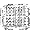
図1は、本発明の第1の実施形態における撮像装置の特徴となる機能構成を示す図である。図1において、100は、エリアイメージセンサ(CMOSイメージセンサ)であり、イメージセンサブロック107と同様な構成のイメージセンサブロック108の2つのブロックから構成されている。101は、画素であり、光電変換により電荷を蓄積し、蓄積した電荷に応じた電気信号を出力する。イメージセンサブロック107、108には、画素101と同様の構成の画素が行列状に並べられている。それらが各列で共通の列信号出力線102に接続され、列信号処理回路103を介して水平出力線104に接続されている。水平出力線104は、再度信号処理回路105を介してエリアイメージセンサ100外部に信号を出力する出力端子に接続されている。イメージセンサブロック107、108の各画素は1行ずつ垂直シフトレジスタ106によって図1に示す矢印の向きに走査される。
FIG. 1 is a diagram illustrating a functional configuration that is a feature of the imaging apparatus according to the first embodiment of the present invention. In FIG. 1,
また、1フレーム遅延回路109は、イメージセンサブロック107が出力する画素データを1フレーム分格納することで、1フレーム遅延させた画素データを出力する。画像処理ブロック110は、1フレーム遅延回路109が出力する画素データと、イメージセンサブロック108が出力する画素データを基に、再生画像データを生成し出力する。
The 1-
図2は、図1に示した撮像装置におけるエリアイメージセンサ100からの画素データの読み出しタイミングダイアグラム例を示す図である。図2において、上ブロックがイメージセンサブロック107を示し、下ブロックがイメージセンサブロック108を示す。尚、図2では上下ブロックとも画素が5行5列の配列となっているが、これは説明及び図面を簡略化したためであり、実際には画素数が数百万画素のエリアイメージセンサであれば数千行数千列となる。
FIG. 2 is a diagram illustrating an example of a timing diagram for reading pixel data from the
また、本実施形態の撮像装置は、動画像を撮影するため、各エリアセンサブロックの最終行が読み出された後は、次のフレームにおける最初の行を再度読み出す。従来は上下ブロックとも同じ第Nフレーム(Nは整数)の画像を用いて最終画像を構築していたため、図3(a)に示すような動く被写体を撮像すると、図3(b)に示すような不連続性な図形になってしまっていた。 In addition, in order to capture a moving image, the imaging apparatus according to the present embodiment reads the first row in the next frame again after the last row of each area sensor block is read. Conventionally, since the final image is constructed using an image of the same Nth frame (N is an integer) in both the upper and lower blocks, when a moving subject as shown in FIG. 3A is imaged, as shown in FIG. It became a discontinuous figure.
しかし、本実施形態における撮像装置は、1フレーム遅延回路109で、上ブロック(イメージセンサブロック107)の出力が1フレーム分遅延するので、画像処理ブロック110は、上ブロックの第Nフレームと、下ブロックの第N+1フレームを足し合わせて最終画像を再生する。これにより、図2に示すように、上ブロックにおいてタイミングt1で蓄積開始された画素データと、下ブロックにおいてタイミングt2で蓄積開始された画素データが足し合わされる。それらの蓄積タイミングは、図2において「蓄積」に下線を付与して示すように、上ブロックと下ブロックの間で連続性のある蓄積タイミングとなっている。すなわち、上ブロックの第Nフレームの最終行の蓄積開始・終了時間と、下ブロック第N+1フレームの最初の行の蓄積開始・終了時間の時間関係は、各行間におけるずれ時間が等しい。これにより、図3の(d)に示したような連続性を有する(不連続性のない)再生画像を得ることができる。
However, in the imaging apparatus according to the present embodiment, the output of the upper block (image sensor block 107) is delayed by one frame by the one-
以上に説明したように、本実施形態における撮像装置は、各行の蓄積時間の開始と終了タイミングが一致しない撮像素子であって、列方向に2分割したブロック構成を有し、独立して各ブロックを走査することで画素データを出力する撮像素子を備えおり、列方向に2分割された一方のブロック(最初に画素が読み出される方)からの画素データを1フレーム分遅延させることで、各行における蓄積時間の開始と終了タイミングを連続的に一定に変化したものにすることができる。これにより、少なくとも垂直方向に2分割したブロック構成を有し、独立して各ブロックを走査するエリアイメージセンサ100での撮像時に、従来は解消できなかった動く被写体の一部に現れる不連続性を解消することができる。
As described above, the imaging device according to the present embodiment is an imaging device in which the start time and end timing of the accumulation time of each row do not match, and has a block configuration divided into two in the column direction. Is provided with an image sensor that outputs pixel data by scanning, and pixel data from one block divided in two in the column direction (the one from which pixels are read first) is delayed by one frame, so that each row The start and end timings of the accumulation time can be continuously changed to be constant. As a result, discontinuities appearing in a part of a moving subject that could not be resolved in the past when imaging with the
また、図1では1フレーム遅延回路109を備える構成を示したが、この構成に限定されるものではない。たとえば1フレーム遅延のための余分なフレームバッファは大きなフレームバッファの一部をしめるメモリにその機能を持たせてもよい。図1に示したブロック構成図はあくまでも機能を説明するためのものであり、回路構成までを限定するものではない。
Although FIG. 1 shows a configuration including the one-
また、上述した実施形態ではCMOSイメージセンサを利用していたが、これに限定されるものではなく、イメージセンサの画素の構成はいかなるものにも限定されない。たとえば画素は、CMD、BASISなどでもよい。また、各画素を走査して画素データを読み出す機能の構成も、種々の構成が考えられる。例えば、列信号処理回路103はゲインアンプやAD変換器、リセットノイズ除去回路などを含んでもよく、また信号処理回路105はバッファやリセットノイズ除去、CDS、AD変換などの機能を有してもよい。
In the above-described embodiment, the CMOS image sensor is used. However, the present invention is not limited to this, and the pixel configuration of the image sensor is not limited to any one. For example, the pixel may be CMD, BASIS, or the like. Various configurations of the function of scanning each pixel and reading out pixel data are also conceivable. For example, the column
特にAD変換器をエリアイメージセンサ100の画素配列の列毎に搭載することで、画素データを外部に出力する時間を短縮できる。すなわち、列信号処理回路103はAD変換器を含む構成であることが好ましい。今後、画素の絶対数が多い場合に、フレームレートを上げるためにブロック分割する手法が主になることが想定され、そのような場合は、フレームレートは「一行分の画素データを列信号処理回路103で処理する時間」もしくは「列信号処理回路103で処理された画素データを外部に出力する時間」のいずれか遅いほうで決定される。実際の応用を考えると、後者の「列信号処理回路103で処理された画素データを外部に出力する時間」を短縮することが必要条件であり、その場合に列信号処理回路103にAD変換器を搭載することは特に効果を発揮する。
In particular, by mounting an AD converter for each column of the pixel array of the
また、列信号処理回路103に搭載するAD変換器の種類においても、様々な形態が考えられるが、図6に一例を示したような、「Dual−Slope Integrating AD Converter」(デュアルスロープ積分方式のA/D変換回路)もしくは「Multi−Slope Integrating AD Converter」(マルチスロープ積分方式のA/D変換回路)を用いることが好ましい。これにより、回路の面積を小さく抑えながら高速化を図ることができる。イメージセンサの画素は数ミクロンの間隔で規則的に並べられており、その間隔に従ってAD変換器を含む列信号処理回路103を配置する必要があり、図6のような構成によりAD変換器の回路面積を小さく保つことはより微細な画素サイズに対応することができる。
Also, various types of AD converters mounted on the column
[第2の実施形態]
次に、第1の実施形態における撮像装置が備えるエリアイメージセンサ100とブロックの分割構成が異なる第2の実施形態における撮像装置について説明する。具体的には、第1の実施形態では列に並列方向への分割を行っていなかったため、列数が多いセンサの場合は一列のデータを外部に出力する時間が長くなり、結果としてフレームレートを落としてしまい、所望のレートを達成できない場合が起こり得る。そこで第2の実施形態おける撮像装置として、列方向にも分割し、列数を実効的に減らすことで一列のデータを外部に出力するのに必要な時間を短縮し、所望のフレームレートを達成させることができるイメージセンサを備える撮像装置について説明する。
[Second Embodiment]
Next, an imaging apparatus according to a second embodiment, which is different from the
図4は、第2の実施形態における撮像装置の機能構成ブロックを示す図である。図4に示すように、本実施形態における撮像装置は、エリアイメージセンサ200を備え、動画像が撮影可能な撮像装置である。エリアイメージセンサ200は、4分割されたイメージセンサブロック201〜204から構成されている。また、イメージセンサブロック202、204の出力は、それぞれ1フレーム遅延回路205、206を介して画像処理ブロック207に入力される。尚、各イメージセンサブロック201〜204の内部構成は、図1に示したイメージセンサブロック107と同様であり説明を省略する。また、画像処理ブロック207は、イメージセンサブロック201、203及び1フレーム遅延回路205、206の出力する画像データを基に、再生画像を出力する。
FIG. 4 is a diagram illustrating a functional configuration block of the imaging apparatus according to the second embodiment. As shown in FIG. 4, the imaging apparatus according to the present embodiment is an imaging apparatus that includes an
図5は、図4に示した撮像装置におけるエリアイメージセンサ200からの画素データの読み出しタイミングダイアグラム例を示す図である。図5において、右上ブロックがイメージセンサブロック202を示し、左上ブロックがイメージセンサブロック204を示し、右下ブロックがイメージセンサブロック201を示し、左下ブロックがイメージセンサブロック203を示す。尚、図4では4ブロックとも画素が5行5列の配列となっているが、これは説明及び図面を簡略化したためであり、実際には画素数が数百万画素のエリアイメージセンサであれば数千行数千列となる。
FIG. 5 is a diagram showing an example of a timing diagram for reading pixel data from the
図5に示すように、イメージセンサブロック201〜204は、それぞれ同一のタイミングで蓄積の開始と終了が行われる。回路的には走査方向(右左)に分割されているが、走査方向に分割したことは読み出しスピードの向上以外に副産物を生み出さない(不連続な画像の原因とはならない)ために、右左のブロック間で蓄積時間をずらすことは考慮しなくてよい。第1の実施形態と同様の原理で、上下のブロック分割において一方のブロックの出力を遅延させて、他方のブロックの出力と一連性のある出力にできればよい。 As shown in FIG. 5, the image sensor blocks 201 to 204 start and end accumulation at the same timing. Although the circuit is divided in the scanning direction (right and left), the division in the scanning direction produces no by-products other than improved reading speed (it does not cause discontinuous images), so the right and left blocks There is no need to consider shifting the accumulation time between. Based on the same principle as in the first embodiment, it is only necessary to delay the output of one block in the upper and lower block divisions so that the output of the other block is a series of outputs.
尚、上述した実施形態においては、行方向に2分割したブロック構成例や行方向及び列方向にそれぞれ2分割したブロック構成例を示したが、これに限定されるものではなく、行方向及び列方向における分割数は2には限定されない。 In the above-described embodiment, the block configuration example divided into two in the row direction and the block configuration example divided into two in the row direction and the column direction are shown. However, the present invention is not limited to this. The number of divisions in the direction is not limited to two.
[第3の実施形態]
次に、図1や図4に示した撮像装置のより具体的な実施形態として、ビデオカメラの実施形態を第3の実施形態として説明する。
図7は、本発明の第3の実施形態におけるビデオカメラ(撮像装置)の概略構成を示した図である。図7において、1は撮影レンズであり、焦点調節を行うためのフォーカスレンズ1A、ズーム動作を行うズームレンズ1B、結像用のレンズ1Cを備えている。
[Third Embodiment]
Next, as a more specific embodiment of the imaging apparatus shown in FIG. 1 or FIG. 4, an embodiment of a video camera will be described as a third embodiment.
FIG. 7 is a diagram showing a schematic configuration of a video camera (imaging device) according to the third embodiment of the present invention. In FIG. 7,
2は、絞りであり、3は、撮像面に結像された被写体像を光電変換して電気的な撮像信号に変換する固体撮像素子である。ここで、固体撮像素子3は、第1、第2の実施形態で説明したエリアイメージセンサ100、200と同様の構成である。4は、固体撮像素子3より出力された撮像信号をサンプルホールドし、さらに、レベルをアンプするサンプルホールド回路(S/H回路)である。このサンプルホールド回路は、映像信号を出力する。
2 is a stop, and 3 is a solid-state image sensor that photoelectrically converts an object image formed on the imaging surface into an electrical imaging signal. Here, the solid-state imaging device 3 has the same configuration as the
5は、サンプルホールド回路4から出力された映像信号にガンマ補正、色分離、ブランキング処理等の所定の処理を施すプロセス回路であり、輝度信号Yおよびクロマ信号Cを出力する。プロセス回路5から出力されたクロマ信号Cは、色信号補正回路21で、ホワイトバランス及び色バランスの補正がなされ、色差信号R−Y,B−Yとして出力される。また、プロセス回路5から出力された輝度信号Yと、色信号補正回路21から出力された色差信号R−Y,B−Yは、エンコーダ回路(ENC回路)24で変調され、標準テレビジョン信号(例えばNTSC信号)として出力される。そして、図示しないビデオレコーダ、あるいは電子ビューファインダ等のモニタEVFへと供給される。
A
次いで、6はアイリス制御回路で有り、サンプルホールド回路4から供給される映像信号に基づいてアイリス駆動回路7を制御し、映像信号のレベルが所定レベルの一定値となるように、絞り2の開口量を制御すべくigメータ8を自動制御するものである。13、14は、サンプルホールド回路4から出力された映像信号中より合焦検出を行うために必要な高周波成分を抽出する異なった帯域制限のバンドパスフィルタ(BPF)である。第一のバンドパスフィルタ13(BPF1)、及び第二のバンドパスフィルタ14(BPF2)から出力された信号は、ゲート回路15及びフォーカスゲート枠信号で各々でゲートされ、ピーク検出回路16でピーク値が検出されてホールドされると共に、論理制御回路17に入力される。この信号を焦点電圧と呼び、この焦点電圧によってフォーカスレンズ1Aを制御してフォーカスを合わせている。
Next,
また、18はフォーカスレンズ1Aの移動位置を検出するフォーカスエンコーダ、19はズームレンズ1Bの焦点距離を検出するズームエンコーダ、20は絞り2の開口量を検出するアイリスエンコーダである。これらのエンコーダの検出値は、システムコントロールを行う論理制御回路17へと供給される。論理制御回路17は、設定された合焦検出領域内に相当する映像信号に基づいて、被写体に対する合焦検出を行い焦点調節を行う。即ち、各々のバンドパスフィルタ13、14より供給された高周波成分のピーク値情報を取り込み、高周波成分のピーク値が最大となる位置へとフォーカスレンズ1Aを駆動すべくフォーカス駆動回路9にフォーカスモータ10の回転方向、回転速度、回転/停止等の制御信号を供給し、これを制御する。
以上、この発明の実施形態について図面を参照して詳述してきたが、具体的な構成はこの実施形態に限られるものではなく、この発明の要旨を逸脱しない範囲の設計等も含まれる。 The embodiment of the present invention has been described in detail with reference to the drawings. However, the specific configuration is not limited to this embodiment, and includes designs and the like that do not depart from the gist of the present invention.
1 撮像レンズ
5 プロセス回路
17 論理制御回路
24 ENC回路
100、200 エリアイメージセンサ
101 画素
102 列信号出力線
103 列信号処理回路
104 水平出力線
105 再度信号処理回路
106 垂直シフトレジスタ
107、108、201、202、203、204 イメージセンサブロック
109、205、206 1フレーム遅延回路
110、207 画像処理ブロック
1
Claims (5)
前記撮像素子の列方向に2分割された一方のブロックが出力する画素データに対して前記フレーム単位の遅延を与えるフレーム遅延手段と、
前記フレーム遅延手段により遅延を与えられた画素データ及び他方のブロックが出力する画素データを基に画像データを生成する画像データ生成手段と
を具備し、
前記撮像素子は、前記一方のブロックの第Nフレームの最終行の蓄積開始・終了時間と、前記他方のブロックの第N+1フレームの最初の行の蓄積開始・終了時間との時間関係が、前記一方のブロックの各行間におけるずれ時間と等しくなるように、前記最初の行の画素を走査することを特徴とする撮像装置。 A group of pixels arranged in a matrix is composed of a plurality of blocks divided into at least two in the column direction, and includes a vertical signal output line commonly connected to pixels in each column direction in each block, and the row direction An image sensor that scans pixels and outputs pixel data in frame units;
Frame delay means for giving a delay in frame units to pixel data output from one block divided into two in the column direction of the image sensor;
Image data generating means for generating image data based on the pixel data delayed by the frame delay means and the pixel data output by the other block , and
The image sensor has a time relationship between the accumulation start / end time of the last row of the Nth frame of the one block and the accumulation start / end time of the first row of the (N + 1) th frame of the other block. An image pickup apparatus that scans the pixels in the first row so as to be equal to a shift time between each row of the block .
前記画像データ生成手段が生成した画像データを標準テレビジョン信号に変換する変換手段と
を具備することを特徴とする請求項1に記載の撮像装置。 An optical system for forming a subject image on the light receiving surface of the image sensor;
The imaging apparatus according to claim 1, further comprising: a conversion unit that converts the image data generated by the image data generation unit into a standard television signal.
Priority Applications (1)
| Application Number | Priority Date | Filing Date | Title |
|---|---|---|---|
| JP2004277798A JP4724400B2 (en) | 2004-09-24 | 2004-09-24 | Imaging device |
Applications Claiming Priority (1)
| Application Number | Priority Date | Filing Date | Title |
|---|---|---|---|
| JP2004277798A JP4724400B2 (en) | 2004-09-24 | 2004-09-24 | Imaging device |
Publications (3)
| Publication Number | Publication Date |
|---|---|
| JP2006094192A JP2006094192A (en) | 2006-04-06 |
| JP2006094192A5 JP2006094192A5 (en) | 2010-04-22 |
| JP4724400B2 true JP4724400B2 (en) | 2011-07-13 |
Family
ID=36234730
Family Applications (1)
| Application Number | Title | Priority Date | Filing Date |
|---|---|---|---|
| JP2004277798A Expired - Fee Related JP4724400B2 (en) | 2004-09-24 | 2004-09-24 | Imaging device |
Country Status (1)
| Country | Link |
|---|---|
| JP (1) | JP4724400B2 (en) |
Families Citing this family (7)
| Publication number | Priority date | Publication date | Assignee | Title |
|---|---|---|---|---|
| JP2010252118A (en) * | 2009-04-16 | 2010-11-04 | Panasonic Corp | Solid-state image pickup element |
| JP5460248B2 (en) * | 2009-11-10 | 2014-04-02 | パナソニック株式会社 | Solid-state image sensor |
| WO2010119702A1 (en) | 2009-04-16 | 2010-10-21 | パナソニック株式会社 | Solid-state image pickup element and method of driving same |
| JP5398610B2 (en) * | 2010-03-19 | 2014-01-29 | 富士フイルム株式会社 | Solid-state electronic imaging device and operation control method thereof |
| JP2014023114A (en) * | 2012-07-23 | 2014-02-03 | Nikon Corp | Imaging device and program |
| US9679929B2 (en) | 2012-10-12 | 2017-06-13 | Samsung Electronics Co., Ltd. | Binary image sensors including quantum dots and unit pixels thereof |
| US9082368B2 (en) | 2012-10-12 | 2015-07-14 | Samsung Electronics Co., Ltd. | Semiconductor devices having image sensor and memory device operation modes |
Family Cites Families (7)
| Publication number | Priority date | Publication date | Assignee | Title |
|---|---|---|---|---|
| JPH06133209A (en) * | 1992-10-20 | 1994-05-13 | Mitsubishi Electric Corp | Turning image pickup device |
| JPH06319080A (en) * | 1993-05-10 | 1994-11-15 | Mitsubishi Electric Corp | Push bloom scanning type image pickup device |
| JP3844806B2 (en) * | 1996-04-26 | 2006-11-15 | 浜松ホトニクス株式会社 | Solid-state image sensor |
| JP2000184282A (en) * | 1998-12-15 | 2000-06-30 | Canon Inc | Image pickup device, drive method for the image pickup device, image processing method, information recording medium and image processing system |
| JP3875423B2 (en) * | 1999-01-19 | 2007-01-31 | 日本放送協会 | Solid-state imaging device and video signal output device therefor |
| JP3507800B2 (en) * | 2001-02-02 | 2004-03-15 | 有限会社リニアセル・デザイン | Analog-digital converter and image sensor using the same |
| JP2003319265A (en) * | 2002-04-26 | 2003-11-07 | Shimadzu Corp | Two-dimensional image detector and two-dimensional image photographing device provided with the same |
-
2004
- 2004-09-24 JP JP2004277798A patent/JP4724400B2/en not_active Expired - Fee Related
Also Published As
| Publication number | Publication date |
|---|---|
| JP2006094192A (en) | 2006-04-06 |
Similar Documents
| Publication | Publication Date | Title |
|---|---|---|
| JP5247007B2 (en) | Imaging apparatus and imaging system | |
| US7436343B2 (en) | Solid state image pickup apparatus, camera and driving method of solid state image pickup apparatus | |
| JP4423112B2 (en) | Solid-state imaging device and imaging system | |
| JP2006217213A (en) | Method and device for physical information acquisition | |
| US8120567B2 (en) | Shift register, and solid state image sensor and camera using shift register | |
| JP2009017459A (en) | Ccd solid-state imaging element, driving method thereof, and imaging apparatus | |
| JP4724400B2 (en) | Imaging device | |
| JP2005109994A (en) | Imaging device | |
| JP4916271B2 (en) | Solid-state imaging device and electronic information device | |
| JP2000106678A (en) | Image pickup device | |
| JP4745677B2 (en) | Imaging device | |
| JP5627728B2 (en) | Imaging apparatus and imaging system | |
| JP2007134806A (en) | Solid-state imaging element | |
| JP2007143067A (en) | Image sensing device and image sensing system | |
| JP2006303856A (en) | Solid state image sensor and imaging apparatus | |
| JP4227596B2 (en) | Pulse generation circuit, imaging device and camera | |
| JP2006121165A (en) | Imaging apparatus and image forming method | |
| JP2006041867A (en) | Image processing method and image processor, imaging apparatus, and timing controller | |
| JP5072466B2 (en) | Imaging device | |
| JP2005295422A (en) | Digital camera device | |
| JP2003008996A (en) | Solid-state electronic image pickup device and its control method | |
| JP2002152597A (en) | Solid-state image pickup device and solid-state image pickup equipment | |
| JP2008124886A (en) | Imaging apparatus with smear reducing function, and smear reducing method | |
| JP2010016450A (en) | Image capturing apparatus | |
| JP2009188819A (en) | Imaging apparatus and control method thereof |
Legal Events
| Date | Code | Title | Description |
|---|---|---|---|
| A621 | Written request for application examination |
Free format text: JAPANESE INTERMEDIATE CODE: A621 Effective date: 20070925 |
|
| A521 | Request for written amendment filed |
Free format text: JAPANESE INTERMEDIATE CODE: A523 Effective date: 20100305 |
|
| A977 | Report on retrieval |
Free format text: JAPANESE INTERMEDIATE CODE: A971007 Effective date: 20100318 |
|
| A131 | Notification of reasons for refusal |
Free format text: JAPANESE INTERMEDIATE CODE: A131 Effective date: 20100330 |
|
| A521 | Request for written amendment filed |
Free format text: JAPANESE INTERMEDIATE CODE: A523 Effective date: 20100528 |
|
| TRDD | Decision of grant or rejection written | ||
| A01 | Written decision to grant a patent or to grant a registration (utility model) |
Free format text: JAPANESE INTERMEDIATE CODE: A01 Effective date: 20110405 |
|
| A01 | Written decision to grant a patent or to grant a registration (utility model) |
Free format text: JAPANESE INTERMEDIATE CODE: A01 |
|
| A61 | First payment of annual fees (during grant procedure) |
Free format text: JAPANESE INTERMEDIATE CODE: A61 Effective date: 20110411 |
|
| FPAY | Renewal fee payment (event date is renewal date of database) |
Free format text: PAYMENT UNTIL: 20140415 Year of fee payment: 3 |
|
| R150 | Certificate of patent or registration of utility model |
Free format text: JAPANESE INTERMEDIATE CODE: R150 |
|
| LAPS | Cancellation because of no payment of annual fees |