JP4700773B2 - A sequence support mechanism for use in switch-based multiprocessor systems. - Google Patents
A sequence support mechanism for use in switch-based multiprocessor systems. Download PDFInfo
- Publication number
- JP4700773B2 JP4700773B2 JP34092498A JP34092498A JP4700773B2 JP 4700773 B2 JP4700773 B2 JP 4700773B2 JP 34092498 A JP34092498 A JP 34092498A JP 34092498 A JP34092498 A JP 34092498A JP 4700773 B2 JP4700773 B2 JP 4700773B2
- Authority
- JP
- Japan
- Prior art keywords
- memory
- node
- processor
- address
- command
- Prior art date
- Legal status (The legal status is an assumption and is not a legal conclusion. Google has not performed a legal analysis and makes no representation as to the accuracy of the status listed.)
- Expired - Fee Related
Links
Images


Classifications
-
- G—PHYSICS
- G06—COMPUTING; CALCULATING OR COUNTING
- G06F—ELECTRIC DIGITAL DATA PROCESSING
- G06F9/00—Arrangements for program control, e.g. control units
- G06F9/06—Arrangements for program control, e.g. control units using stored programs, i.e. using an internal store of processing equipment to receive or retain programs
- G06F9/46—Multiprogramming arrangements
- G06F9/52—Program synchronisation; Mutual exclusion, e.g. by means of semaphores
Description
【0001】
【発明の属する技術分野】
本発明は、一般に、コンピュータアーキテクチャーの分野に係り、より詳細には、分散型共用メモリマルチプロセッサシステムに係る。
【0002】
【従来の技術】
この分野で良く知られているように、対称型のマルチプロセッサコンピュータは、高性能のアプリケーション処理を行うことができる。通常の対称型マルチプロセッサコンピュータシステムは、バスによって互いに接続された多数のプロセッサを備えている。対称型マルチプロセッサシステムの1つの特徴は、メモリ空間が全てのプロセッサ間で共用されることである。1つ以上のオペレーティングシステムがメモリに記憶され、種々のプロセッサ間でのプロセッサ又はスレッドの分散を制御する。
異なるプロセッサ又はスレッドが多数の異なるプロセスを同時に実行できるようにすることにより、所与のアプリケーションの実行速度を著しく高めることができる。理論的に、システムの性能は、マルチプロセッサシステムにおけるプロセッサの台数を増加するだけで改善することができる。実際には、ある飽和点を越えてプロセッサを追加し続けると、単に通信ボトルネックが増えるだけとなり、従って、全システム性能を制限することになる。
【0003】
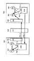
例えば、図1Aには、共通の相互接続バスを経て互いに接続された8個のプロセッサを含む典型的な公知のマルチプロセッサシステム2が示されている。動作中に、各プロセッサ3a−3hは、共用相互接続バス5を経て互いに他のプロセッサ及び共用メモリ4と通信する。図1Aの対称型マルチプロセッサ構成は、今日までに構築されたマルチプロセッサについて充分である。しかしながら、より高速のマイクロプロセッサの出現に伴い、通常の共用相互接続バスは、接続されたマイクロプロセッサの潜在的な全性能を充分に働かせることができない。プロセッサとメモリとの間の唯一の通信リンクは、共用バスであるから、バスはプロセッサからの要求で急速に飽和状態となり、各プロセッサがシステムバスへのアクセスを得るよう試みるときに遅延が増大する。それ故、プロセッサは、高い速度で動作することができるが、性能に関する制限ファクタは、システムバスの使用可能な帯域である。
【0004】
通信帯域巾は、SMPシステムの性能において重要なファクタである。帯域巾は、SMPシステムにおけるノードの対又はサブセットの間で均一ではないから、業界では、SMPシステムの通信帯域巾を決定するために「二等分帯域巾」測定を使用している。二等分帯域巾は、次のように決定される。システムを等しい計算能力(等しいプロセッサ数)の2つの部分に区分化する全ての考えられる方法が確かめられている。各区分に対し、2つの区分間に維持し得る帯域巾が決定される。全ての維持し得る帯域巾の最小値は、相互接続の二等分帯域巾である。2つの区分間の最小帯域巾は、最悪の通信パターンが存在するときにマルチプロセッサシステムにより維持できる通信帯域巾を指示する。従って、大きな二等分帯域巾が望まれる。
【0005】
公知技術では、バス飽和の問題を克服するために、多数の相互接続アーキテクチャー即ち「トポロジー」が使用されている。これらのトポロジーは、メッシュ、トーラス(円環体)、ハイパーキューブ(超立体)及び拡張ハイパーキューブを含む。
【0006】
【発明が解決しようとする課題】
例えば、メッシュ相互接続は、図1Bにシステム7として示されている。メッシュネットワークの主な利点は、簡単で且つ配線が容易なことである。各ノードは、少数の他の隣接ノードに接続される。しかしながら、メッシュ相互接続は、3つの重大な欠点を有する。第1に、メッセージは、それらの行先に到達するために平均的に多数のノードを横断しなければならず、その結果、通信の待ち時間が長くなる。第2に、二等分帯域巾は、他のトポロジーに対するものであるから、メッシュトポロジーの場合に充分に計測しない。最後に、各メッセージはメッシュ内の異なる経路を進行するので、SMPシステム内には自然の順序付けポイントが存在せず、それ故、メッシュトポロジーの実施を必要とするキャッシュコヒレンスプロトコルがしばしば非常に複雑なものとなる。
【0007】
トーラス、ハイパーキューブ及び拡張ハイパーキューブトポロジーは、全て、ノードが種々の複雑な構成、例えば円環体構成又は立体構成で相互接続されたトポロジーである。トーラス、ハイパーキューブ及び拡張ハイパーキューブの相互接続は、メッシュ相互接続よりも複雑であるが、その待ち時間及び帯域巾は、メッシュ相互接続よりも優れている。しかしながら、メッシュ相互接続と同様に、トーラス、ハイパーキューブ及び拡張ハイパーキューブトポロジーは、自然の順序付けポイントを与えず、従って、これらのシステムの各々に対して複雑なキャッシュコヒレンスプロトコルを実施しなければならない。
共用メモリのマルチプロセッサシステムでは、プロセッサは、通常、将来アクセスされる見込みが高いと決定されたデータを記憶するために専用キャッシュを使用している。プロセッサは、それらの専用キャッシュからデータを読み取りそしてメモリへ書き戻すことなく専用キャッシュにおいてデータを更新するので、各プロセッサの専用キャッシュが一貫して即ちコヒレントに保持されるよう確保するための機構が必要となる。SMPシステムのデータのコヒレンス性を確保するのに使用される機構は、キャッシュコヒレンスプロトコルと称される。
【0008】
物理的な相互接続部のトポロジー、帯域巾及び待ち時間に加えて、キャッシュコヒレンスプロトコルの効率も、システム性能の重要なファクタである。キャッシュコヒレンスプロトコルは、待ち時間、ボトルネック、非効率性又は複雑さを多数の仕方で導入する。
ロード及び記憶動作の待ち時間は、設計のプロトコルによって直接影響されることがしばしばある。例えば、あるプロトコルでは、全ての無効化メッセージがそれらのターゲットプロセッサへ送られそして確認メッセージがその元のプロセッサへ完全に返送されるまで記憶動作が完了したとみなされない。従って、記憶の待ち時間は、無効化がその行先へ送られるのを元のプロセッサが待機しなくてよいプロトコルよりも相当に長いものとなる。更に、確認は、システム帯域巾の相当の部分を消費する。
【0009】
ボトルネックは、コントローラの高い占有度によりしばしば生じる。「占有度」とは、コントローラが要求を受け取った後に使用できなくなる時間の長さを示す用語である。あるプロトコルでは、直接的なコントローラは、メモリ位置に対応する要求を受け取ると、その前のコマンドに対応するある確認がディレクトリに到着するまで同じメモリ位置への他の要求に対して使用できなくなる。コントローラは、平均より高いレートで競合する要求を受け取る場合に、ボトルネックとなる。
又、キャッシュコヒレンスプロトコルの設計は、ハードウェアの複雑さにも影響する。例えば、あるプロトコルは、停滞及び公正さの問題を招き、これらは、付加的な機構で対処される。その結果、ハードウェアの複雑さが増大する。
【0010】
そこで、オペレーションの待ち時間を最小にし、広い通信帯域巾を与え、コントローラの占有度を低くし、そして多数のプロセッサへと拡張することのできる対称的なマルチプロセッサシステムを提供することが要望される。
【0011】
【課題を解決するための手段】
本発明は、少なくとも1つのプロセッサ及び共用メモリの一部分を含む多数のマルチプロセッサノードがスイッチを経て互いに接続された対称的なマルチプロセッサシステムに効果的に使用される。マルチプロセッサノードの各々にはトランザクション追跡(トラッキング)テーブル(TTT)が維持される。TTTは、ノードをスイッチに接続するノードのグローバルポートに存在してもよいし、或いはマルチプロセッサノードの少なくとも1つのプロセッサの各々に存在してもよい。
TTTは、マルチプロセッサノードから発生され及びそれにより受け取られる要求の順序を決定しそしてそれを強制するのに使用される。本発明の1つの特徴によれば、TTTは、マルチプロセッサノードへ返送される要求の順序を次のように決定するのに使用される。各要求は、多数のトランザクションに細分化され、各トランザクションは、異なる仮想チャンネルを経て搬送される。少なくとも1つのチャンネルが順序付けされるが、他のチャンネルの返送データは、ばらばらの順序で受け取ることができる。コヒレンス性を維持するために、共通のアドレスへ発生されるトランザクションが順序正しく取り扱われるのが望ましい。本発明の1つの特徴によれば、マーカーパケットが、順序付けされたチャンネルを経てTTTへ発生され、アドレスに関連したデータが依然処理されていることを指示する。このような構成では、TTTは、マーカーパケットに続いて受け取られた上記順序付けされたチャンネルの他の要求を無視するか、又はデータが受け取られるまで遅延するように確保する。
【0012】
従って、本発明の1つの特徴によれば、各々少なくとも1つのプロセッサ及び共用メモリの一部分を含む複数の接続されたマルチプロセッサノードを有するコンピュータシステムは、上記複数のマルチプロセッサノードの各々における複数のプロセッサに関連した追跡機構であって、上記複数のマルチプロセッサノードの1つにおける少なくとも1つのプロセッサの1つにより発生された共用メモリのリモート部分のアドレスへの要求の位置を、上記複数の接続されたマルチプロセッサノードにおける少なくとも1つのプロセッサにより上記アドレスへ発生された複数の他の要求に対して識別するための追跡機構を備えている。
本発明の更に別の特徴によれば、マルチプロセッサコンピュータシステムの共通のアドレスへ発生される複数の要求間の順序を維持するための方法が提供される。マルチプロセッサコンピュータシステムは、スイッチを経て接続された複数のマルチプロセッサノードを備え、各マルチプロセッサノードは、少なくとも1つのプロセッサ及び共用メモリの一部分を含む。上記方法は、マルチプロセッサノードの各々からスイッチへ送られる要求のアドレスリストを維持して、リモートマルチプロセッサノードの共用メモリの一部分における各アドレスに対して要求の相対的な順序を識別し、アドレスに関連した要求が満足されるまでアドレスをリストに維持するという段階を含む。
【0013】
【発明の実施の形態】
本発明の上記及び他の特徴は、添付図面を参照した以下の詳細な説明から明らかとなろう。
本発明の1つの実施形態によれば、ハイアラーキー式の対称的マルチプロセッサ(SMP)システムは、高性能スイッチを経て互いに接続された多数のSMPノードを備えている。従って、SMPノードの各々は、SMPシステムにおいてビルディングブロックとして働く。以下、1つのSMPノードビルディングブロックの要素及び動作を最初に説明し、その後に、SMPシステムの動作を説明し、それに続いて、大規模のSMPシステムにおいてメモリのコヒレンス性を維持するために使用されるキャッシュコヒレンスプロトコルを説明する。
【0014】
SMPノードビルディングブロック
図2を参照すれば、マルチプロセッサノード10は、4つのプロセッサモジュール12a、12b、12c及び12dを備えている。各プロセッサモジュールは、中央処理ユニット(CPU)を備えている。好ましい実施形態では、デジタル・イクイップメント社で製造されたAlpha(登録商標)21264プロセッサチップが使用されるが、以下に述べるコヒレンスプロトコルをサポートすることのできるものであれば、他の形式のプロセッサチップも使用できる。
マルチプロセッサノード10は、多数のメモリモジュール13a−13dを含むメモリ13を備えている。このメモリは、32ギガバイトの記憶容量を備え、4つのメモリモジュールの各々が8ギガバイトを記憶する。各メモリモジュールは、多数のメモリブロックに分割され、各ブロックは、例えば、64バイトのデータを含む。データは、一般に、メモリからブロックで検索される。
【0015】
更に、マルチプロセッサノード10は、接続されたI/Oバス14aを経て外部装置(図示せず)とマルチプロセッサノード10との間で行われるデータ転送を制御するためのI/Oプロセッサ(IOP)モジュール14を備えている。本発明の1つの実施形態では、I/Oバスは、周辺コンピュータ相互接続(PCI)プロトコルに基づいて動作する。IOP14は、IOPキャッシュ14c及びIOPタグ記憶装置14bを含む。IOPキャッシュ14cは、PCIバス14aを経て外部装置へ転送されるメモリ13からのデータのための一時的な記憶装置である。IOPタグ記憶装置14bは、外部装置とプロセッサとメモリとの間に移動されるデータに対するコヒレンス情報を記憶するための64エントリのタグ記憶装置である。
【0016】
マルチプロセッサノードのメモリ13に記憶されたデータのコヒレンス性は、デュープリケートタグ記憶装置(DRAG)20によって維持される。DTAG20は、全てのプロセッサ12a−12dにより共用され、そして4つのバンクに分割される。各バンクは、関連するプロセッサにより使用されるデータに対応する状態情報を専用に記憶する。
DTAG、メモリ及びIOPは、ARBバス17と称する論理バスに接続される。プロセッサにより発生されるメモリブロック要求は、ローカルスイッチ15を経てARBバス17にルート指定される。DTAG20及びIOP14は、プロセッサ及びIOPのキャッシュにおけるブロックの状態をルックアップし、そしてメモリブロックに対しそれらの状態を原子的に更新する。ARBバス17は、全てのメモリ参照に対してシリアル化ポイントとして働く。メモリ要求がARBバスに現れる順序は、プロセッサが要求の結果を認知する順序である。
【0017】
プロセッサモジュール12a−12d、メモリモジュール13a−13d及びIOPモジュール14は、ローカルの9ポートスイッチ15を経て互いに接続される。インターフェイスモジュール12a−12d、13a−13d及び14の各々は、同数の両方向性クロック送信データリンク16a−16iによりローカルスイッチに接続される。1つの実施形態では、データリンクの各々は、150MHzのレートで動作するシステムクロックの各縁で64ビットのデータ及び8ビットのエラー修正コード(ECC)を送信する。従って、データリンク16a−16iの各々のデータ帯域巾は、2.4ギガバイト/sである。
ローカルスイッチ15は、クオドスイッチアドレス制御チップ(QSAチップ)18及びクオドスイッチデータスライスチップ(QSDチップ)19を備えている。QSAチップ18は、プロセッサモジュールIOPとメモリとの間のアドレス経路を制御するためのアービター(QS ARB)11を備えている。更に、QSAチップ18は、以下に述べるようにローカルスイッチ15を通るデータの流れを制御するためにQSDチップ19を制御する。QSDチップ19は、プロセッサモジュールと、メモリモジュールと、IOPとの間の全てのデータ経路に対するスイッチ相互接続を与える。図2には示されていないが、以下に述べるように、マルチプロセッサノード10がグローバルポートを経て他のマルチプロセッサノードに接続された場合には、QSD及びOSAがグローバルポートに対するスイッチ相互接続部を付加的に形成する。各プロセッサは、メモリデバイス13a−13d、他のプロセッサ12a−12d、IOP14のような使用可能なリソースの1つからデータを要求することもできるし、或いは他のマルチプロセッサノードのリソースからグローバルポートを経てデータを要求することもできる。従って、ローカルスイッチ15は、2.4ギガバイトの広いバス帯域巾を維持しながら、種々のリソースから同時入力を受け入れることができねばならない。
【0018】
ローカルスイッチは、多数の同時トランザクションを取り扱うことができる。各トランザクションは、通常、多数のリソース(メモリバンクや、データ経路や、待ち行列のような)を使用するので、ローカルスイッチの制御機能は非常に複雑になる。例えば、あるトランザクションは、そのトランザクションの段階0でメモリバンクを使用でき、段階1でメモリバンクからプロセッサポートへのデータ経路を使用でき、そして段階2でプロセッサポートからプロセッサへのデータ経路を使用できることを必要とする。ローカルスイッチアービター(QSA18のQSA ARB11)は、あるトランザクションが開始されると、各段階でトランザクションにより必要とされるリソースが必要に応じて使用できるように要求を裁定する。
【0019】
より重要なことに、アービターは、特定の要求が、他の要求の進行中に長時間にわたり(潜在的に不定に)裁定に負けることのないよう確保することにより、全ての要求及びプロセッサがリソースに対して公平なアクセスを得るように保証する。例えば、3つのリソースA、B及びCを要求するトランザクションTについて考える。このトランザクションTは、トランザクションの適当な段階に3つのリソース全部が使用できるよう保証されるまで裁定に勝てない。リソースが使用可能であることのみに基づいてアービターがその判断を行う場合には、トランザクションTは、A、B又はCの1つを使用する(他のリソースD、E等と共に)他のトランザクションが裁定に勝ち続ける間は、長時間にわたって成功しないことが考えられる。
【0020】
各々が多数のリソースを使用して完了するような非常に多数の同時要求を伴うスイッチにおいて公平な裁定を保証するのは、計算上複雑である上に、高速データ経路において遅延を増加し勝ちである。ここに示す装置においては、QSAARB11が、特定のトランザクションをスケジュールする前に、1つのリソース(メモリバンク)のみについて裁定を行う。プロセッサに通じる待ち行列である第2のリソースは、QSA ARB11により第1のリソースについて裁定を行うときに、それが使用可能であるかどうかについてチェックする必要がない。というのは、QSDのアーキテクチャーがそのデータ経路を保証しそして待ち行列に通じる待ち行列スロットが常に使用できるからである。リソースに対する公平な裁定は、QSAARB11に著しい複雑さを伴うことなく与えられる。
【0021】
本発明の1つの実施形態によれば、QSDは、対応する行先に通じるバッファに対してアップフロント裁定を必要とせずに全てのリソース(プロセッサ、メモリ、IOP及びグローバルポート)からの入力を同時に受け取ることができる。次いで、全てのデータリソースは、データ経路又はスイッチにおける待ち行列スロットへのアクセスを裁定する必要なく、スイッチへデータを独立して送信することができる。というのは、QSDは、全てのリソースからのデータを実質的に同時に受信することのできる多数の同時挿入バッファを備えているからである。同時挿入バッファの2つの実施形態を以下に説明する。
【0022】
同時挿入バッファスイッチ
上記のように、マルチプロセッサノードにおけるプロセッサ12a−12d、IOP14及びメモリデバイス13a−13dの各々は、マルチプロセッサノードのプロセッサ及びIOPからの要求を取り扱うためのリソースとして働く。データは、各リソース要素と、要求を発する要素との間でパケットの形態で転送される。各パケットは、512ビットのデータと、64ビットのECCとを含む。上記したように、各データリンクは、64ビットのデータ及び8ビットのECCを150MHzクロックの各縁において搬送する。従って、QSDの外部には、パケット当たり8個のデータ転送サイクルがある。しかしながら、QSDの内部では、クロックの1つの縁においてのみデータが収集される。従って、QSDの内部のロジックの各クロックサイクルに対し、潜在的に128ビットのデータがデータリンクから受け取られる。各パケットは、512ビットのデータ及び64ビットのECCを含むので、QSDの内部では、各パケットごとに4つのデータ転送サイクルがあり、各QSDクロックサイクルに、128ビットのデータ及び16ビットのECCがプロセッサ、IOP又はメモリデバイスからQSDへ転送される。
【0023】
図3を参照すれば、QSD19は、5つの同時挿入バッファ(SIB)25a−25eを含むように詳細に示されている。各SIBは、要求側要素、即ちプロセッサ12a−12d又はIOPの1つに専用である。各SIBは、それに関連した要求側要素と、ノード内の他のリソース要素、即ちプロセッサ12a−12d、メモリ13a−13d、IOP14及び好ましくはグローバルポートとの間でパケットを転送するためのデータ経路を制御する。グローバルポートは、他のマルチプロセッサノードへの相互接続部として働き、以下に詳細に説明する。SIBは、スイッチへのアクセスに対し要求側要素間の裁定を必要とせずに、スイッチに接続されたいずれのリソースからでも要求側要素によりパケットを同時に受信できるようにする。
【0024】
既に述べたように、QSA ARB11は、スイッチ19への制御を与えるように接続される。QSA ARB11には、メインアービター27が含まれる。このメインアービター27は、リソース(IOP、プロセッサ12a−12d及びメモリ13a−13d)とスイッチ19との間のデータの移動を管理する。プロセッサ12a−12d及びIOP14の各々は、ライン28a−28e上のリソースの1つへアクセスするための要求を発生し、これらは、メインアービター27に送られる。次いで、メインアービターは、各リソースが要求を受信できるときにこれらの要求をその関連リソースへ送る。リソースが要求を受け取るときに、スイッチ19の裁定は必要とされない。というのは、SIBの各々は、全ての入力からの入力を実質的に同時に即ち同じデータサイクル内に受け取ることができるからである。 又、QSA AEB11には、多数の個々のアービター23a−23dも含まれる。これらアービター23a−23dの各々は、プロセッサ12a−12dの関連する1つと、それに対応するSIB25b−25eとの間のデータ路を管理するのに使用される。IOP14とSIB25aとの間のデータ路を管理するために、IOP14には同様のアービター(図示せず)が含まれる。各プロセッサは、その関連SIBからデータを受け取ることができるので、その関連アービターは、接続されたデータ路にデータを送信する。
【0025】
従って、スイッチ19内の同時挿入バッファの使用により、要求側要素とリソースとの間の裁定経路は、2つの別々の区分に分割される。即ち、接続されたりソースからデータを受け取るために要求を発しているプロセッサが使用できるかどうかに拘わりなくプロセッサからの要求に応答してメインアービター27がリソースを裁定するところの第1裁定区分と、プロセッサに関連したアービターがスイッチからのデータを送信するためにプロセッサへのアクセスを裁定するところの第2裁定区分である。このような構成では、裁定が分離されるために、接続されたりソース各々への公平なアクセスが与えられるように保証することができる。
図4Aを参照すれば、SIB25aの1つの実施形態が詳細に示されており、これは、ライン36aを経て8個の接続されたマルチプレクサ34a−34hにMUX選択信号<31:0>を与えるように接続された入力アービター36を備え、MUX選択信号の4つが8個のマルチプレクサの各々に送られて、各マルチプレクサの9個の入力の1つが選択される。SIB25a−25dは全て同様の構造にされ、従って、その1つについてのみ詳細に説明する。上記したように、潜在的に10個のリソースがSIBに接続される。10個のリソースの1つは、SIBから出力を受信する要求側デバイスであり、一方、他の9個のリソースは、SIBに入力を与える。それ故、マルチプレクサ34a−34hの各々は、SIBに接続された9個のリソースから入力を受け取る。接続されたプロセッサの3つからの入力は、ラインPx、Py及びPzを経て受け取られる。第4のプロセッサ(SIBがIOPデバイスに関連するとき)又はIOPデバイス(SIBが1つのプロセッサに関連するとき)からの別の入力はラインPW/IOPを経て受け取られる。メモリバンク13a−13dからの入力は、各々、ラインmem0、mem1、mem2及びmem3を経て受け取られ、そしてグローバルポートからの入力は、グローバルポートラインを経て受け取られる。
【0026】
マルチプレクサ34a−34hの各々からの各出力は、バッファ32の8個のバンクの1つに接続される。各バンクは8個のエントリを有し、各エントリは、128ビットのデータ及び16ビットのECCを記憶する。従って、SIBにより受信されるデータの各パケットは、バッファ32の同じ行において4つの異なるバンクに書き込まれる。以下に述べるように、入力アービター36は、データを記憶するのに使用できるバッファのバンクを指示するための状態ビットを維持する。従って、1つ以上のリソースから128ビットのパケットデータが受け取られる各サイクルごとに、入力アービター36は、バンクの使用状態に基づいて関連バンク32a−32hへパケットデータのサイクルを送信するために、各マルチプレクサ34a−34hにおける考えられる9個のリソース入力の1つを選択する。又、入力アービターは、ライン36bを経てマルチプレクサ30へバイパスデータも与える。入力アービターの状態ビットが、全てのバンク32a−32hが空であることを指示するときには、9個のリソース入力の1つが入力アービター36を経て関連する要求側要素へ直接バイパスされる。
【0027】
バンク32a−32hの各々は、マルチプレクサ30に接続される。マルチプレクサ30は、出力アービター38により制御される。SIB25aに関連する要求側要素がSIBからデータを受け取る準備ができ、そしてパケットの一部分がSIBのエントリに書き込まれると、出力アービターは、バンク32a−32hから要求側要素に8個のエントリーの1つを供給する。或いは又、出力アービターは、いずれのバンクも転送保留データをもたずそして入力アービターからライン36bを経てデータが得られる場合には、ライン36bを経て要求側要素にバイパスデータを供給する。
動作中に、パケットデータの第1の128ビットがSIBに受け取られたときに、8個のバンクの1つが、パケットデータの第1の128ビットを記憶するために選択される。本発明の1つの実施形態によれば、パケットデータの128ビットが受け取られる次の3サイクルの各々の間に、手前の書き込みを実行するのに使用したバンクに隣接するバンクが、パケットデータの次の128ビットを書き込むのに選択される。例えば、バンク32aが、ソースmem0からパケットデータの第1サイクルを書き込むのに使用できるバンクとして選択された場合には、パケットデータの第2サイクルはバンク32bに書き込まれ、第3サイクルはバンク32cに書き込まれ、そして第4サイクルはバンク32dに書き込まれる。従って、パケットデータのその後のサイクルを書き込むためにどのバンクを使用すべきかの選択は、入力アービターにより選択されたバンクでスタートしそして各次々のパケット書き込みに対して隣接バンクに続くようにして回転ベースで実行される。その結果、受け取られたパケットがバッファ32の共通の行における4つのバンクにわたって分散される。
【0028】
8個のバンクが設けられ、そして本発明の1つの実施形態では、いずれの要求側要素においても保留となり得るリソース読み取りの最大数は8であるから、各書き込みサイクルの間に各リソースに対して少なくとも1つのバンクを使用できることが確保される。それ故、所与の瞬間に、全部で8個の保留の読み取り応答がスイッチによって受け取られた場合に、バンク32a−32hの各々を使用して、第1のパケットデータ書き込みサイクルを受け入れることができ、バンクの選択は、次の3つの書き込みサイクルについて回転される。
本発明の1つの実施形態では、SIBの各バッファは、先入れ先出し(FIFO)プロトコルのもとで動作する。パケットの2つの部分が同時に受け取られるので、それらに対しスイッチへ「読み込まれる」順序が選択される。リソースに対して裁定を行う要求側要素のロジックは、SIBと通信せず、そしてリソースに対して裁定するための他の要求側要素とも通信しないので、標準的なルールに従ってデータの完全性を確保する。例えば、リソースに固定の優先順位番号が指定される場合には、「低い番号の入力リソースからのデータが、常に、高い番号の入力リソースからのデータの前にスイッチに書き込まれる」というようなルールに従う。
【0029】
上記のように、図4Aに示すSIBの実施形態では、8個のバンクの使用について説明した。というのは、要求側要素が所与の瞬間にもつことのできる保留メモリ要求の数が8に対応するからである。しかしながら、設計上の制約により、それより少数のバンクを設けることが必要な場合には、インターリーブ又は同様の技術を使用して多数のデータチャンクを共通のバンクの異なる位置に同時に書き込みできるように当業者によって容易に設計を変更することができよう。それ故、本発明は、図4Aに示す特定の実施形態に限定されるものではない。
上記のように、動作中に、入力アービターは、リソースからデータを書き込むための適当なバンクを選択するためにバンクにおける入力の利用性に関する状態情報を維持する。SIBへの入力を制御するための入力アービター36の実施形態が図4Bに示されている。上記では9個の入力リソースについて述べたが、図4Bには、明瞭化のために、2つのリソース入力のみの書き込みを制御するロジックが示されている。入力パケットデータがライン35を経て受け取られるときに、「入力1」のような指示信号がラッチチェーン40に送られ、このラッチチェーンは、4個のラッチ、フリップ−フロップ又は同様の状態装置を含む。ラッチチェーン40は、カウンタ機構として使用される。この例の目的として、4つの次々のデータ転送サイクルにパケットデータが受け取られると仮定する。4つのデータ転送サイクルの間に、入力信号はラッチチェーンを経て伝播する。ラッチチェーンには、オアゲート46が接続される。入力値がラッチチェーン40を経て伝播するときに、オアゲート46の出力がアサートされる。
【0030】
オアゲート46の出力は、シフトレジスタ48へのシフト信号を与える。シフトレジスタは、SIBの各バンクについて1つづつ、8個のビット位置を含む。シフトレジスタ48は、入力信号サンプルを最初に受信する際に、バンク選択ロジック44からのビットベクトルがロードされる。バンク選択ロジック44から受け取られたビットベクトルは、1ビットがセットされるだけであり、ベクトル内のビットの相対的な位置が、パケットデータの書き込みを開始すべきバンクを指示する。
従って、バンク選択ロジック44は、パケットデータの第1サイクルの書き込み行先を制御する。バンク選択ロジック44は、利用性ベクトル42を入力として受け取り、利用性ベクトルにおけるビットの相対的な位置が、書き込みデータを受け取ることのできない関連バッファを指示する。
【0031】
バンク選択ロジックがシフトレジスタ48へビットを与えるときに、シフトレジスタ48の値がデマルチプレクサ49に送られる。又、デマルチプレクサ49は、入力1ソースが接続されるところのマルチプレクサ34a−34hの入力の数値表示も入力として受け取る。例えば、デマルチプレクサ49は、「1」のマルチプレクサ選択値を用いてマルチプレクサ34aを経て入力1リソースデータが送られることを指示する「1」入力値を受け取る。選択されたバンクを指示するシフトレジスタ内のビットの位置に基づいて、値「1」がMUX選択<31:0>信号36aの適当な位置へ伝播される。各入力ソースに対する各デマルチプレクサは、全てのMUX選択信号を駆動し、それらの出力は、これらの信号がマルチプレクサ34a−34hを駆動する前にオアされる。
【0032】
バンクエントリの書き込みの後に、シフトレジスタの内容がオアゲート50によりオアされ、利用性バンクベクトル42として記憶される。これは、次のサイクルの間に、どのバンクが到来する書き込みに対して使用できるかをバンク選択ロジック44により決定するために使用される。
ライン46aのシフト信号がアサートされる各サイクルに、シフトレジスタ48のビットが右へシフトされる。ビットが右へシフトするときには、MUX選択信号<31:0>の選択値も右へシフトされ、次の書き込み動作中に入力ソースを次の隣接バンクへ供給するようにさせる。
従って、ローカルQSDスイッチ内のSIBを使用することにより、多数の同時に受け取られた入力がそれらの行先である要求側要素へ到達するように確保できる簡単且つ効率的なスイッチング機構が設けられる。このような構成では、リソースへのアクセスに対してソースがいったん裁定されると、ソースにより実行されねばならない全ての裁定が完了する。ソースは、リソースが常にスイッチバッファ32へのアクセスを得ることができるという事実に依存する。ソースアービターが互いに独立して動作してリソースを管理できることにより、最小限の複雑さで公平な裁定を確保する機構が設けられる。更に、SIBは、要求側要素の最大数の保留中読み取りに対してデータを記憶できるので、たとえ全てのリソースからデータが同時に受け取られても、バッファ32に対するリソースを裁定する必要はなく、リソースロジックの全体的な複雑さが低減される。
【0033】
図5には、図3に示すようにプロセッサ又はIOPデバイス(キャッシュを含む任意の要求側デバイス)へ接続することのできる同時挿入バッファ(SIB)61の第2の実施形態が示されている。SIB61は、9個のマルチプレクサ60a−60iを含み、そのうちの8個は、8個のバッファ62a−62hの各々に接続される。第9マルチプレクサ60iは、以下に述べるようにバイパス経路を与えるのに使用される。マルチプレクサ60a−60iの各々は、接続されたメモリデバイスmem0−mem3からの4つの入力、グローバルポートからの1つの入力、接続されたプロセッサからラインPx、Py及びPzを経て送られる3つの入力、そしてIOP(SIBに関連したデバイスがプロセッサの場合)又は別のプロセッサ(SIBに関連したデバイスがIOPの場合)からラインPW/IOPを経て送られる1つの入力を含む9つの入力を受け取る。
【0034】
バッファ62a−62hの各々は、4つの128ビットエントリを含む。従って、各入力バッファは、SIBにおいて次々のサイクル中に4つの128ビット部分で受け取られた1つの512ビット情報パケットを記憶する。各バッファには、4対1のマルチプレクサ64a−64hが各々接続される。これらのマルチプレクサ64a−64hは、関連バッファの4つの入力のうちの1つを選択して、マルチプレクサ66を経てSIBの出力へ供給するのに使用される。
図4Aについて上述したように、本発明の1つの実施形態では、各要求側要素がいかなる所与の瞬間にも異なるリソースに対してせいぜい8個の保留中読み取り参照を有するだけであるから、8個のバッファが含まれる。従って、図5には8個のバッファが示されているが、本発明はこれに限定されるものではない。むしろ、選択されるバッファの数は、関連するプロセッサ又はIOPデバイスのバッファ特性に依存する。
【0035】
動作中に、接続されたりソースの各々から入力が受け取られるときに、入力アービター67は、各マルチプレクサにおける入力ラインの1つを選択し、データのパケットを空きバッファへ供給する。所与のリソースからのパケット書き込みの時間中に同じバッファが選択され、パケットの全ての部分が単一のバッファに維持される。パケットの少なくとも1つの部分がバッファに書き込まれると、それがマルチプレクサ66に送られ、関連する要求側要素の準備ができたときにその要求側要素へ供給される。或いは又、いずれのバッファにもパケットデータが存在しない場合には、マルチプレクサ60iを経、マルチプレクサ66を経てパケットデータを出力へ直接的に供給することによりバイパス経路を選択することができる。
【0036】
8個のバッファが設けられるので、SIBデバイス61は、接続されたりソースの各々から実質的に同時に(即ち、同じデータサイクルに)データを受け取ることができる。QSDにSIBを使用することにより、前記の実施形態の場合のように、SIBへのアクセスに対し要求側要素の間に裁定は必要とされない。その結果、リソースがローカルスイッチを使用する準備ができたときにローカルスイッチの利用性が保証される。更に、本来的に公平な裁定機構が設けられる。というのは、スイッチに対する裁定の結果としてリソースへの要求が他のリソースへの他の要求により阻止されないからである。従って、裁定の複雑さを最小限に抑えながら最大のバス帯域巾を維持することのできる公平で且つ比較的簡単な構造体が与えられる。
【0037】
従って、同時挿入バッファを使用して広いバス帯域巾をサポートするローカルスイッチを実施することにより処理リソースを最適に使用するマルチプロセッサノード10が提供される。更に、ARBバス13において参照の順序がシリアル化されるので、マルチプロセッサ10のメモリのコヒレンス性を容易に維持する中央順序付けポイントが設けられる。ローカルスイッチに接続されるプロセッサモジュールの数を増加することにより処理能力を高める可能性が存在するので、図2の4プロセッサ/ローカルスイッチ構成体は、待ち時間の短いそしてコストの安い高性能のシステムを提供する。
【0038】
大型の対称的マルチプロセッサシステム
モノリシックマルチプロセッサノードに含むことのできるプロセッサの数は、2つのファクタにより制限される。第1に、ローカルスイッチを経て互いに接続できるプロセッサの数は、ローカルスイッチを構成するチップにおいて使用できるピンの数により制限される。第2に、単一のモノリシックスイッチによりサポートされるデータ帯域巾が制限される。従って、接続されるプロセッサの数をある点を越えて増加すると、何ら性能利得が得られないことになる。
本発明の1つの実施形態によれば、ハイアラーキースイッチを経て複数のマルチプロセッサノードを相互接続することにより大型の対称的なマルチプロセッサシステムを形成することができる。例えば、ハイアラーキースイッチを経て8個のマルチプロセッサノードを接続して、32個のプロセッサモジュール、8個のIOPデバイス及び256ギガバイトのメモリを含む対称的なマルチプロセッサ(SMP)システムが形成される。説明上、ここでは、少なくとも2つのマルチプロセッサノードを含むSMPを大型SMPと称する。以下に詳細に述べるように、SMPノードにローカルスイッチを用いて少数のプロセッサを接続し、そしてハイアラーキースイッチを用いて多数のノードを大型のSMPへと接続することにより、拡張可能な高性能システムを実現することができる。
【0039】
マルチプロセッサノードをハイアラーキースイッチ式ノードへと接続するために、マルチプロセッサは、グローバルなポートインターフェイスを含むように拡張される。例えば、図6には、変更されたマルチプロセッサノード100が示されている。図2のマルチプロセッサノードと同様に、ローカルスイッチ110は、4つのプロセッサモジュール、4つのメモリモジュール及びIOPモジュールを接続する。図2及び6の同様の要素は、同じ参照番号を有する。マルチプロセッサノード100のローカルスイッチ110は、図2のポート16a−16iと同様に構成された9個のポート116a−116iを含む10ポートスイッチである。付加的なポート116jは、グローバルリンク132を経てグローバルポート120へ至る全二重のクロック供給データリンクを形成する。
【0040】
グローバルポートは、マルチプロセッサノードをハイアラーキースイッチに接続し、大型のSMPを実現する。例えば、図7Aを参照すれば、本発明の1つの実施形態において、8x8のハイアラーキースイッチ155を経て互いに接続された8個のノード100a−100hを含む大型のSMPシステム150が示されている。これらノード100a−100hの各々は、図6に示すノード100と実質的に同一である。
ノード100a−100hの各々は、全二重クロック供給データリンク170a−170hの各々によりハイアラーキースイッチ155に接続される。1つの実施形態において、データリンク170a−170hは、150MHzのクロック速度で動作され、従って、スイッチ155との間でデータをやり取りするための2.4ギガバイト/秒のデータ帯域巾をサポートする。これは、最大38.4ギガバイト/秒の生の相互接続データ帯域巾、及び19.2ギガバイト/秒の二等分データ帯域巾をスイッチに与える。
【0041】
大型のSMPシステムは、マルチプロセッサノード100a−100hの各々が全システムメモリのアドレス可能な部分を含むか又は物理的メモリの分割部分を含むような分散型共用メモリシステムである。本発明の1つの実施形態では、全システムメモリに243個の物理的アドレス位置が存在する。SMPマルチプロセッサシステム100の1つの実施形態は、「大フォーマット」及び「小フォーマット」と称する2つのアドレスフォーマットをサポートする。大フォーマットは、各ノードのプロセッサが動作するところの43ビットの物理的アドレスを、マルチプロセッサシステムに使用するための43ビットの物理的アドレスに直接マップする。大フォーマットアドレスを使用すると、物理的メモリアドレスのビット<38:36>をノード識別番号として使用することができる。アドレスビット38:36は、メモリスペースアドレスのホームノードを直接デコードし、一方、アドレスビット38:36の逆数は、I/Oスペースアドレスのホームノードをデコードし、ここで「ホーム」とは、メモリスペース又はI/Oスペースに関連したメモリ及びI/Oデバイスが存在するところの物理的マルチプロセッサノードを指す。
【0042】
小フォーマットのアドレスモードは、マルチプロセッサシステムに4つ以下のノードが存在することを仮定するものである。小フォーマットは、各ノードのプロセッサが36ビットの物理的にアドレスされたシステムで動作できるようにする。小フォーマットにおいて、物理的アドレスのビット34:33は、データ又はI/Oデバイスのホームノード番号を識別する。
しかしながら、たとえCPUが36ビットの物理的アドレスを用いて動作しても、マルチプロセッサシステムは、データ位置を特定するのに43ビットの物理的アドレスを一貫して使用し、物理的アドレスのビット37:36がデータ又はI/Oデバイスのホームノード番号を識別する。従って、CPUにより発生された小フォーマットアドレスと、データライン13a−13hを経てハイアラーキースイッチ155へ送信されるものとの間で何らの変換が実行される。
【0043】
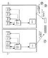
マルチプロセッサシステム150のここに示す構成は、32個のプロセッサ間に広帯域巾のキャッシュコヒレントな共用メモリを与えることができる。本発明の1つの実施形態による大型SMPの別の実施形態が図7Bに示されており、ここでは、2つのマルチプロセッサノード100a及び100bがハイアラーキースイッチを使用せずに互いに接続される。むしろ、2つのマルチプロセッサノードは、それらのグローバルポート出力を互いに接続することにより直接接続される。
図7Bの2ノード実施形態が使用されるか、図7Aのマルチノード実施形態が使用されるかに拘わりなく、大きなアドレススペース及び処理能力をもつマルチプロセッサシステムが得られる。
【0044】
両実施形態において、システムメモリアドレススペース及びI/Oアドレススペースは、全てのノード100a−100h間にセグメントで物理的に分配される。システムの各ノードは、メモリスペースの物理的アドレスの上位3ビットを使用してアクセスされるメインメモリの一部分を含む。従って、各メモリ又はI/Oアドレスは、1つのノードのみにおける1つの唯一のメモリ位置又はI/Oデバイスへとマップされる。従って、上位3つのアドレスビットは、メモリ又はI/Oアドレスがマップされるノードである「ホーム」ノードを識別するためのノード番号を与える。各マルチプロセッサノードは、それらのホームノード又は他のマルチプロセッサノードに記憶された共用メモリの部分をアクセスすることができる。ホームノードがプロセッサ自身のノードであるところの共用メモリブロックにプロセッサがアクセス(ロード又は記憶)するときには、参照は、「ローカル」メモリ参照と称される。ホームノードがプロセッサ自身のノード以外のノードであるようなブロックを参照する場合には、参照は、「リモート」又は「グローバル」メモリ参照と称する。ローカルメモリアクセスの待ち時間は、リモートメモリアクセスの待ち時間と異なるので、SMPシステムは、非均一メモリアクセス(NUMA)アーキテクチャを有すると言える。更に、システムはコヒレントなキャッシュを備えているので、システムは、キャッシュコヒレントなNUMAアーキテクチャと呼ばれる。
【0045】
ここに示すキャッシュコヒレントなNUMAアーキテクチャは、高い性能と低い複雑さに寄与する多数の特徴を含む。設計上の1つの特徴は、メッセージ間の順序の固執及び利用である。メッセージがある順序特性に基づいてシステムに流れるよう保証することにより、オペレーションの待ち時間を著しく短縮することができる。例えば、記憶オペレーションは、記憶が完了したとみなされる前に無効メッセージがそれらの最終的な行先プロセッサに供給されることを必要とせず、むしろ、無効メッセージが行先プロセッサへと通じるある順序付けされた待ち行列に入れられるや否や記憶が完了したとみなされる。
更に、ある順序が維持されるよう保証することにより、設計上、確認又は完了メッセージの必要性が排除される。メッセージは、それらがある待ち行列に入れられた順序でそれらの行先に到達するように保証される。従って、メッセージがその行先に到達したときに確認を返送する必要性が排除される。これは、システムの帯域巾を改善する。
【0046】
更に、事象順序及びメッセージ順序は、「ホットポテト」オペレーションを行うのに使用される。ある待ち行列に順序を利用することにより、ディレクトリ又はDTAGコントローラのようなコントローラは、単一ビジットにおいて要求をリタイアすることができる。他の要求との競合により要求を否定的に確認しそして再トライする必要はない。「ホットポテト」オペレーションの結果として、公平さ及び欠乏の問題が解消される。
設計に使用される第2の特徴は、仮想チャンネルである。仮想チャンネルとは、メッセージを「チャンネル」へと分類する構成であって、チャンネルは物理的なリソースを共用する(従って、「仮想」である)が、各チャンネルは、他のものとは独立して流れ制御される。仮想チャンネルは、システムのメッセージ間で流れに依存しそしてリソースに依存するサイクルを排除することにより、キャッシュコヒレンスプロトコルにおける停滞を排除するのに使用される。これは、選択されたメッセージを否定的に確認しそしてそれに対応するコマンドを再トライすることにより停滞を検出しそして停滞状態を解消する機構を用いた公知のNUMAマルチプロセッサにおけるキャッシュコヒレンスプロトコルとは対照的である。
【0047】
チャンネルの使用について以下に簡単に説明するが、詳細な説明は後で行う。上述したように、メッセージは、「チャンネル」と称する論理的なデータ路を用いて大型SMP内をルート指定される。本発明の1つの実施形態には、以下のチャンネルが含まれる。即ち、要求側プロセッサから、トランザクションのアドレスに対応するホームノードのARBバスへトランザクションを搬送するためのQ0チャンネルと、ホームARBバスから1つ以上のプロセッサ及びIOPへトランザクションを搬送するためのQ1チャンネルと、所有者プロセッサから要求側プロセッサへデータ記入トランザクションを搬送するためのQ2チャンネルとである。変更されたデータを書き込むためにプロセッサからメモリへビクティム(Victim)トランザクションを搬送するためにQ0Vicチャンネルを設けることもできる。更に、Q0Vicチャンネルは、ビクティムトランザクションの背後に保持しなければならないQ0トランザクションを搬送するのに使用できる。最後に、プロセッサからIOPへIOスペーストランザクションを搬送するためにQIOチャンネルが設けられる。
【0048】
チャンネルは、以下に示すようなハイアラーキーを構成する。
(最低)QIO>Q0Vic>Q0>Q1>Q2(最高)
以下に述べるように、停滞を回避するために、いずれのチャンネルのメッセージも、下位チャンネルのメッセージによって決して阻止されてはならない。順序付け特性及び仮想チャンネルを形成しそして使用する機構の設計及び実施に関する詳細は、後で述べる。
従って、図7A及び7Bに示すように、大型SMPは、図2のSMPノードを任意の数だけ互いに接続することにより形成することができる。図7A及び7Bに示すような大型SMPシステムのオペレーションは、以下に3つの部分について説明する。第1に、大型SMPに含まれるハードウェア要素について説明する。次いで、SMPのプロセッサ間にコヒレントなデータ共用を与えるキャッシュコヒレンスプロトコルについて説明する。更に、ハイアラーキースイッチの仮想チャンネルのために設けられたサポート機構を含む仮想チャンネルの実施及び使用について説明する。
【0049】
大型SMPのハードウェア要素
マルチプロセッサノードの各々には、チャンネルを用いてコヒレントなデータ共用を実施するための多数の要素が設けられる。図6に戻ると、これらの要素は、ディレクトリ140と、DTAG20と、IOPタグ14bと、グローバルポート120と、ディレクトリ140とを備えている。更に、シリアル化ポイントのハイアラーキーは、キャッシュコヒレンスプロトコルを容易にするために参照の順序を維持できるようにする。これら要素の各々について、以下に詳細に述べる。
グローバルポート
グローバルポート120は、マルチプロセッサノード100を、ハイアラーキースイッチリンク170を経て1つ以上の同様に構成されたマルチプロセッサノードに直接接続できるようにする。各ノード100は対称的なマルチプロセッサシステムとして動作するので、システムにより多くのノードが追加されるにつれて、使用可能なアドレススペース及び処理能力が増加される。
【0050】
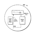
図8は、グローバルポート120の拡張ブロック図である。グローバルポートは、トランザクション追跡テーブル(TTT)122と、ビクティムキャッシュ124と、マルチプロセッサノードからハイアラーキースイッチへ送られるパケットを記憶するためのパケット待ち行列127、122、123及び125と、ハイアラーキースイッチから受け取られるパケットを記憶するためのパケット待ち行列121とを備えている。グローバルポート120は、ARBバス130と、ローカルスイッチの2つの専用ポート即ちGPリンク入力132b及びGPリンク出力132aとを経てノードの他のロジック(特にQSAチップ)と通信する。
TTTは、マルチプロセッサノードにおいて保留中のトランザクション、即ちノードからグローバルポートを経て発生されて、他のマルチプロセッサノード又はハイアラーキースイッチからの応答を待機しているトランザクションを追跡する。グローバルポートにコマンドが送られるたびに、TTTにエントリが形成される。対応する応答がノードに受け取られたときに、TTTエントリがクリアされる。TTTは、2つの部分、即ちQ0TTT及びQ1TTTで構成され、Q0及びQ1は、上記のようにQ0及びQ1チャンネルを進むパケットを指す。エントリーがTTTにいかに割り当てられるか及びそれがいつリタイアされるかについては、以下に詳細に述べる。
【0051】
又、グローバルポート120は、ビクティムキャッシュ124を含む。ビクティムキャッシュ124は、マルチプロセッサノードの各プロセッサから受け取られて別のマルチプロセッサノードのメモリに向けられるビクティム化データを記憶する。ビクティム化データとは、プロセッサのキャッシュ位置に記憶されてそのプロセッサにより変更されたデータである。変更データを記憶するキャッシュ位置に記憶する必要のある新たなデータがプロセッサに受け取られると、変更データは、ビクティム化されると言われ、ビクティムデータと称される。
ビクティムキャッシュ124は、プロセッサからリモートマルチプロセッサノードのメモリへ向けられたビクティムデータからのビクティムデータの一時的な記憶装置である。グローバルポートを経て別のノードへビクティムデータを送信するための機会があるときには、マルチプレクサ167は、ビクティムキャッシュ124からバス170の出力部分にデータを供給するように切り換えられる。グローバルポートにビクティムキャッシュを設けることにより、個々のプロセッサがグローバルシステムのメモリ書き込み待ち時間を待機せずに、プロセッサが各々のビクティムデータバッファを空にすることができる。むしろ、ビクティム書き込みは、使用できるデータサイクルがあるときに書き込みが実行されるようにグローバルポートにより制御される。ビクティムキャッシュからデータを解放する適切さに関連した幾つかの制御の問題があるが、これらは以下に説明する。
【0052】
DTAG及びIOPタグ
DTAG及びIOPタグは、小型のSMPシステムにも含まれるが、これについては以下に詳細に述べる。DTAG20は、マルチプロセッサノードのプロセッサのキャッシュに記憶されたデータブロック各々に対する状態情報を記憶する。同様に、IOタグ14aは、IOPに記憶された各データブロックに対する状態情報を記憶する。ディレクトリは、どのマルチプロセッサノードがデータのコピーを記憶するかを識別するおおよその情報を与えるが、DTAG及びIOタグは、マルチプロセッサノード内のどのプロセッサがデータのコピーを記憶するかに関する正確な指示を与えるのに使用される。それ故、DTAG及びIOタグは、参照情報がマルチプロセッサノードに到達したときに、そのノードのどのプロセッサがターゲットとなるべきかを決定するのに使用される。
【0053】
図6に示すように、DTAG20及びIOPタグ14bは、QSAチップ18に接続されたメモリ領域を参照するアドレスを監視するためにARBバス130に接続される。DTAGは、4つのプロセッサ12a−12dに対応する4つのセグメントに分割される。各プロセッサは、メモリ13からのデータのサブセットを一時的に記憶するためのキャッシュ(図示せず)を備えている。各プロセッサのキャッシュに記憶されたメモリのブロックの上位アドレスビット(タグ)を記憶するためのタグ記憶装置が各キャッシュに関連される。DTAG20の各セグメントは、関連プロセッサのキャッシュタグの状態を指示するデータを維持する。処理ユニットの外部のDTAG20にタグのコピーを記憶することにより、システムは、ARBバスを経て受け取ったコマンドをフィルタし、そしてプロセッサのキャッシュのデータに関連した調査(読み取り)及び無効化コマンドのみを各プロセッサに供給することができる。IOPタグ14aは、IOPキャッシュ14cに記憶されたデータブロック各々の上位アドレスビットを記憶する。IOPタグ記憶装置は、プロセッサ12a−12dの各々に維持されたタグ記憶装置と同様である。
【0054】
DTAG20及びIOPタグ14aの各エントリは、多数の状態ビットを含む。DTAG状態ビットは、次の4つの状態、即ちInvalid(無効)、Clean(クリーン)、Dirty Not Probed、及びDirty Probedのうちの1つを指示する。IOPタグのエントリの状態ビットは、次の2つの状態、即ちValid(有効)及びDirty(ダーティ)のうちの1つを指示する。「有効」ビットは、関連キャッシュの対応エントリに記憶されたデータが、メモリに記憶されたデータと一致することを指示する。「ダーティ」ビットは、関連キャッシュの対応エントリに記憶されたデータが関連プロセッサによって変更されそしてメモリに記憶されたデータに一致しないことを指示する。
【0055】
DTAG20及びIOPタグ14bは、マイクロプロセッサノード100のARBバスにコマンドが現れるたびにアクセスされる。「無効」の状態がプロセッサ1のDTAGアクセスに応答して返送される場合には、ノードのプロセッサ1は、メモリアドレスに関連したデータの有効コピーを記憶しない。「有効」の状態がIOPタグ14aへのアクセスから返送される場合には、IOPキャッシュ14cがデータの有効コピーを記憶する。「クリーン」状態がプロセッサ1に対するDTAGアクセスに応答して返送される場合には、これは、プロセッサ1がメモリアドレスに対応するデータの無変更コピーを有するが、そのデータを読み取るための他のプロセッサによる試みがなされていないことを指示する。Dirty Not Probedの状態がDTAGに応答して返送される場合には、これは、プロセッサ1がメモリアドレスに対応するデータの変更コピーを有し、そしてプロセッサが最後にデータを変更して以来、少なくとも1つのプロセッサがデータを読み取る試みをしていることを指示する。
【0056】
ディレクトリオペレーション
一般に、ディレクトリは、関連マルチプロセッサノード(ホームノード)におけるメモリの各ブロックの所有権情報を与えるのに使用され、メモリのブロックは、一般に、メモリとSMPシステムのプロセッサとの間に転送される最小量のデータである。例えば、本発明の1つの実施形態において、ブロックは、パケットのサイズと同様であり、即ち512ビット(64バイト)のデータである。更に、ディレクトリは、どのマルチプロセッサノードがメモリデータのブロックのコピーを記憶するかを指示する。従って、読み取り型のコマンドの場合に、ディレクトリは、データの最新バージョンの位置を識別する。ビクティム型のコマンドの場合には、データの変更ブロックがメモリに書き戻される場合に、ディレクトリは、データの変更ブロックが現在のものであってメモリに書き込まねばならないかどうか決定するために検討される。それ故、ディレクトリは、参照情報がリモートマルチプロセッサノードのプロセッサにより発生されたものであるかローカルマルチプロセッサノードのプロセッサにより発生されたものであるかに拘わりなく、関連するマルチプロセッサノードのメモリブロックへの参照に対する第1アクセスポイントである。
【0057】
ディレクトリは、対応するノード100においてメモリ13の各64バイトのデータブロック(以下、キャッシュラインとも称する)に対して1つの14ビットエントリを記憶する。メモリ13と同様に、ディレクトリは、メモリアドレスがノードNに存在する場合に、対応するディレクトリエントリもノードNに存在するように、システムのノードにわたって物理的に分配される。
図9を参照すれば、ディレクトリエントリ140aの1つの実施形態は、所有者IDフィールド142及びノード存在フィールド144を含むように示されている。所有者IDフィールドは、各64バイトブロックに対する6ビットの所有者情報を含む。所有者IDは、ブロックの現在所有者を特定し、現在所有者は、システムにおける32個のプロセッサの1つ、又はシステムにおける8個のI/Oプロセッサの1つ、又はメモリのいずれかである。8ビットのノード存在情報は、システムの8個のノードのどれがキャッシュラインの現在バージョンを獲得したか指示する。ノード存在ビットは、同じノードにおける4つのプロセッサの累積状態を1ビットで表わすおおよそのベクトルである。共用データの場合には、2つ以上のノードが、情報を記憶する少なくとも1つのプロセッサを有する場合に、2つ以上のノード存在ビットがセットされる。
【0058】
時々、状態情報のある断片がDTAG又はディレクトリから得られる。このような場合、DTAGからの状態情報を使用するのが好ましい。というのは、これは非常に高速で検索されるからである。例えば、メモリアドレスの所有者プロセッサがそのアドレスに対しホームノードに配置される場合には、所有者IDを供給するのにDTAGが使用される。
性能上の理由でDTAGによりサービスされない情報又は参照については、ディレクトリ140は、全てのコヒレンス性判断の焦点であり、従って、多数の機能を実行する。ディレクトリは、メモリデータブロックの所有者を識別する。所有者は、プロセッサ又はメモリのいずれかである。ディレクトリからの所有者情報は、データブロックの最新バージョンのソースを決定するために読み取り型コマンド(例えば、読み取り、読み取り−変更)により使用される。又、所有者情報は、以下に詳細に述べるようにビクティム化データをメモリに書き戻さねばならないかどうか決定するのにも使用される。
【0059】
全ての読み取り型コマンドに対して、データの所有者を識別するのに加えて、ディレクトリは、プロセッサからの「クリーン−ダーティ(Clean-to-Dirty)」及び「シェアド−ダーティ(Shared-to-Dirty)」コマンドを分析するのにも使用される。「クリーン−ダーティ」コマンドは、プロセッサがそのキャッシュにおいて現在「クリーン」状態にあるキャッシュラインを変更するよう希望するときにプロセッサにより発生される。「シェアド−ダーティ」コマンドは、「ダーティ−シェアド」状態にあるキャッシュラインを変更するよう希望するときに発生される。これらのコマンドは、ホームARBバスに送られ、そこで、ディレクトリは、プロセッサがキャッシュラインの最新バージョンを有するかどうか決定する。もしそうであれば、コマンドは成功となり、プロセッサは、キャッシュラインを変更することが許される。さもなくば、コマンドは失敗となり、プロセッサは、最初に、キャッシュラインの最新バージョンを獲得しなければならない。これらの記憶型オペレーションは、ディレクトリのノード存在情報を使用して、成功又は失敗を決定する。
【0060】
上記のように、ディレクトリの存在ビットは、記憶型コマンドが発生されたときに各データブロックのコピーでマルチプロセッサノードを識別する。記憶コマンドは、キャッシュラインの内容が更新されようとしていることを指示する。関連するディレクトリエントリの存在ビット144を検討することにより、記憶コマンドがディレクトリ140に受け取られたときに、存在ビットを有するノードを用いて、これらのマルチプロセッサノードをそのノードにおけるキャッシュラインのコピーで識別し、従って、各ノードにおけるキャッシュラインを無効化できるようにする。
従って、ディレクトリ及びDTAGは、ローカルマルチプロセッサのメモリにおける各データブロック及びローカルプロセッサのキャッシュに記憶された各データブロックに対する状態情報を与えるように協働する。ホームノードのディレクトリは、キャッシュブロックのコピーの状態に関するおおよその情報を供給する。次いで、無効化コマンドがディレクトリにより識別されたノードへと進み、そこで、DTAGがアクセスされて、コピー情報を更に改善する。従って、これらノードにおけるDTAGは、各ノードのどのプロセッサがそれらのキャッシュにラインのコピーを記憶するか指示する。
【0061】
TTT:
TTTは、マルチプロセッサノードからの保留中のトランザクション、即ち別のマルチプロセッサノード又はハイアラーキースイッチからの応答を待機している参照を追跡するのに使用される。保留中トランザクションに関する情報は、関連メモリアドレスへのその後のコマンドを処理する際にキャッシュコヒレンスプロトコルにより使用される。
図10を参照すれば、TTT122の1つの実施形態は、アドレスフィールド152と、コマンドフィールド154と、コマンダIDフィールド156と、ビット158a−158cを含む多数の状態ビット158とを含むように示されている。アドレスフィールド152は、現在進行中であるトランザクションに対するキャッシュラインのアドレスを記憶し、一方、コマンドフィールドは、現在進行中であるトランザクションに対するキャッシュラインに関連したコマンドを記憶する。コマンダIDフィールド156は、コマンドフィールドに記憶されたコマンドを開始したプロセッサのプロセッサ番号を記憶する。状態ビット158は、コマンドが進行中であるときにコマンドの状態を表わす。或いは又、状態ビット158は、進行中であるコマンドの種々の特性をあらわすように使用されてもよい。
【0062】
例えば、「記入」状態ビット158aは、読み取り型コマンドに応答して「記入」データ応答が受け取られたときに更新される。「シャドー」状態ビット158bは、グローバルポートを経て発生されたコマンドが「シャドー」型コマンド(以下に詳細に述べる)である場合にセットされる。ACK状態ビット158cは、確認型応答を期待しているメッセージが応答を受信した場合にセットされる。応答が到着した場合に、このビットはクリアされる。TTTに含むことのできる全ての状態ビットが示されているのではないことに注意されたい。むしろ、以下の説明に関連のある状態ビットが含まれている。更に、メモリのコヒレンス性を維持するために必要と考えられれば、他の状態ビットを設けてもよく、従って、本発明は、TTTにおける特定のビット指定に限定されるものではないことが明らかであろう。
【0063】
従って、ディレクトリ、DTAG、IOPタグ及びTTTの各々は、SMPシステムにおけるキャッシュラインのコヒレンス性(以下、キャッシュコヒレンス性と称する)を維持するのに使用される。これら要素の各々は、ハイアラーキースイッチ155に接続されたマルチプロセッサノード間にコヒレント通信を与えるためにグローバルポートとインターフェイスする。
【0064】
シリアル化ポイント:
上記要素に加えて、各マルチプロセッサノードにシリアル化ポイントを設けることによりデータ共用コヒレンス性が維持される。本発明の1つの実施形態において、各マルチプロセッサノードにおけるシリアル化ポイントは、ARBバス130である。全てのQ0参照は、ローカルプロセッサにより発生されたものであるかリモートプロセッサにより発生されたものであるかに拘わりなく、QSAによりARBバス130を経てディレクトリ140及びDTAG20へ供給される。参照がディレクトリ及び/又はDTAGをアクセスすると、それにより得られるQ1チャンネルコマンドが厳密な順序でARBバスに出力され、ここで、順序は参照のシリアル化順序である。マルチプロセッサノードの各々にシリアル化ポイントを設けることにより、SMPにおいて実施されるデータ共用コヒレンスプロトコルが相当に簡単化される。
【0065】
マルチプロセッサノードの各々にシリアル化ポイントを設けるのに加えて、ハイアラーキースイッチ155は、SMPシステムに第2のシリアル化ポイントを与える。以下に詳細に述べるように、ハイアラーキースイッチは、第1のシリアル化ポイントに導入されたコヒレンス性が大型のSMPシステムに維持されるよう確保するある順序付けルールに適合する。 グローバルポート/ハイアラーキースイッチインターフェイス:
図11は、8個の入力ポート155i0−155i7及び8個の出力ポート155o0−155o7を含むハイアラーキースイッチ155のブロック図である。ハイアラーキースイッチ155の入力ポート155i0−155i7は、接続されたマルチプロセッサノード各々のグローバルポートからパケットを受け取る。ハイアラーキースイッチの出力ポート155o0−155o7は、接続されたマルチプロセッサノード各々のグローバルポートへパケットを供給する。
【0066】
本発明の1つの実施形態において、受信したパケットをバッファするためのバッファ160a−160hが各入力ポートに関連される。図11の実施形態は、各入力に1つのバッファを示しているが、いかなる数の入力ポート間にバッファが共用されてもよい。各パケットは、5つのチャンネルのいずれか1つと関連される。本発明の1つの実施形態では、以下に述べるように、各入力バッファ160a−160hの部分が、あるチャンネルのパケットを専用に記憶するようにされる。従って、グローバルポートからハイアラーキースイッチ155への流れ制御は、チャンネルベースで実行される。チャンネルベースでスイッチへのデータの流れを制御しそして入力バッファの部分を選択されたチャンネルに専用とすることにより、スイッチは、SMPシステムにおけるマルチプロセッサノード間で停滞のない通信を行う。
【0067】
停滞のない通信を与えるのに加えて、ハイアラーキースイッチ155は、更に、メモリのコヒレンス性を確保するためにSMPシステムの順序付け制約をサポートするように設計される。順序付け制約は、スイッチ155から関連マルチプロセッサノードのグローバルポートへ送出されるパケットの順序を制御することにより課せられる。いずれかの入力バッファ160a−160hからのパケットは、マルチプレクサ182a−182hを経ていずれかの出力ポートへ送られる。更に、以下に述べるように、スイッチ155は、パケットをマルチキャスティングすることができる。従って、1つの入力バッファからのパケットは、いかなる数の出力ポートに送ることもできる。グローバル出力ポートに順序を強制することにより、マルチプロセッサノード各々に得られるシリアル化順序を維持して、完全にコヒレントなデータ共用機構をSMPシステムに形成することができる。
【0068】
ハイアラーキースイッチにおける停滞の回避
上述したように、図7Aの8個のノードの各々は、ハイアラーキースイッチにデータを供給し、全てのノードがデータを同時に供給することもある。パケットは、異なる仮想チャンネルに供給される多数の異なるチャンネル形式(Q0、Q0Vic、Q1、Q2及びQIO)に分割され、ここで、仮想チャンネルとは、本質的に、他のチャンネルとの共通の相互接続部を共用するがその相互接続部のいずれかの端において独立してバッファされる特定形式のパケットに専用のデータ経路である。各ノードのグローバルポートとハイアラーキースイッチとの間には1つのデータ経路しかないので、異なる仮想チャンネルからの全てのパケットは、1つのデータ経路を使用してハイアラーキースイッチに書き込まれる。
【0069】
8個のノード100a−100hの各々は、ハイアラーキースイッチへデータを送信することができるので、全てのメッセージがスイッチにより受信されて、スイッチから適当な順序で供給されるよう適切に確保するために、ある形式の制御が必要となる。更に、本発明の1つの目的は、対称的なマルチプロセッサシステムに停滞(デッドロック)が生じないよう保証するために上位順序のパケット形式が下位順序のパケット形式により阻止されないよう確保することである。本発明の1つの実施形態では、最高順序から最低順序までのパケットの順序は、Q2、Q1、Q0、Q0Vic及びQIOである。
本発明の1つの特徴によれば、スイッチの入力ポートに到着するパケットの流れ制御を行うための機構であって、上記の停滞回避ルールが常に満足されるよう確保する機構が提供される。更に、スイッチにおいて使用できるバッファは最適に利用されねばならず、そして最大の帯域巾が維持されねばならない。
【0070】
本発明の1つの実施形態によれば、ハイアラーキースイッチへのデータの書き込みを制御するための制御装置は、パケットの各形式に対し、ハイアラーキースイッチのバッファに専用スロットを設けることにより実施される。又、バッファは、任意の形式のパケットを記憶するのに使用できる多数の一般的なスロットも含んでいる。ハイアラーキースイッチに専用のバッファスロットを設けることにより、上位順序のパケット形式が常にスイッチを通る経路を使用できるよう保証することによって停滞を回避することができる。更に、使用できる一般的スロット及び専用スロットの数を監視し、そしてバッファに記憶されるパケットの異なる形式の数を監視することにより、ハイアラーキースイッチのバッファが容量に達したときにノードがバッファに書き込みするのを防止するような簡単な流れ制御機構を実施することができる。
【0071】
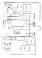
図12Aには、多数のソースノードによる共通の行先バッファへの書き込みを制御するのに使用するための制御ロジックの一例が示されている。図12Aのブロック図には、2つの異なるノードのグローバルポート120a及び120bが一例として示されている。
図12Aにおいて、ノード100a及び100bのグローバルポート各々120a及び120bの部分は、ハイアラーキースイッチ155へ転送するためにQ0/Q0Vic、Q1、Q2及び一般形式のパケット(Q0、Q0Vic、Q1、Q2又はQIOパケットのいずれか)を各々記憶するためのエントリ135a−135bを含むバッファ135を備えて詳細に示されている。バッファ135にはマルチプレクサ167aが接続され、GPアービター134からの選択信号を使用してリンクを経てハイアラーキースイッチへ送るためにパケット形式の1つを選択する。
【0072】
更に、各グローバルポートは、専用のカウントレジスタ136を備えている。この専用のカウントレジスタは、パケットの各Q0/Q0Vic、Q1及びQ2チャンネル形式に対して、ハイアラーキースイッチ155において現在保留となっているチャンネル形式のパケットの数のカウントを記憶する。このカウントは、各チャンネル形式のパケットがハイアラーキースイッチへ転送されるときに増加され、そしてパケットがハイアラーキースイッチから転送されるときに減少される。
本発明の1つの実施形態において、ハイアラーキースイッチ155は、8個の入力ソースの各々に1つのバッファを備えている。図12Aには、2つのグローバルポート120a及び120bに対応する2つのバッファ160a及び160bのみが示されている。本発明の1つの実施形態では、バッファ160a及び160bの各々に少なくとも(m−1)xn個の専用スロットがあり、但し、mは、バッファに専用エントリを有する仮想チャンネル形式の数に対応し、そしてnは、バッファを共用するノードの数に対応する。図12Aの実施形態において、各バッファは、8個のエントリを有する。エントリのうちの5つは、一般的エントリであり、グローバルポート135から送られたパケットの形式を記憶することができる。残りの3つのエントリの各々は、特定形式のパケットを専用に記憶し、即ち1つのエントリは、Q0/Q0Vicパケットを専用に記憶し、1つのエントリは、Q1形式パケットを専用に記憶し、そして1つのエントリは、Q2形式パケットを専用に記憶する。
【0073】
専用エントリがバッファ160a及び160bの固定位置に存在するものとして示されているが、実際には、バッファのいずれの位置も専用のバッファ位置であり、即ちエントリの位置に拘わりなく、パケットの各特定形式ごとにバッファには常に1つの専用エントリがある。
ハイアラーキースイッチは、更に、各バッファ160a及び160bに対し、専用カウンタ162a及び162bと、フラグレジスタ163a及び163bとを含む。図12Aの実施形態において、専用カウンタ162aは、4つのエントリを有し、その3つは、バッファ160aに現在記憶されているQ0/Q0Vic、Q1及びQ2パケットの数を記憶するためのもので、そして1つは、バッファに使用される一般的エントリの数のカウントを記憶するためのものである。フラグレジスタは、3つのビットを含み、各ビットは、パケットのQ0/Q0Vic、Q1及びQ2形式の1つに対応し、そして関連する専用カウントがゼロであるかどうか(即ち、その形式のパケットの専用エントリが使用されたかどうか)を指示する。従って、フラグレジスタの値は、その形式の少なくとも1つのパケットがバッファに記憶されたことを指示する1であるか、又はその形式のパケットがバッファに記憶されないことを指示する0である。
【0074】
更に、ハイアラーキースイッチ155は、各バッファ160a及び160bに対し、トランシットカウント164a及び164bを各々含む。トランシットカウントは、各ソースに対して、所与のデータサイクル中にトランシット状態であるいずれかの形式の保留中パケットの数を維持する。
所与のデータサイクル中にトランシット状態にあるパケットの数は、ハイアラーキースイッチとグローバルポートとの間の流れ制御待ち時間に直接関係している。流れ制御信号は、ハイアラーキースイッチからグローバルポートへ送られて、ハイアラーキースイッチへのデータの送信を停止するようにグローバルポートに通知する。流れ制御待ち時間(L)は、ハイアラーキースイッチによる流れ制御信号のアサートと、グローバルポートによるデータ送信の停止との間に生じるデータ転送サイクルの数として測定される。
【0075】
又、ハイアラーキースイッチは、各バッファ168a及び168bの書き込みを制御するための書き込み制御ロジック166a及び166bも備えている。この書き込み制御ロジックは、ライン168aに「流れ制御」信号をそしてライン168bに「確認(ACK)」信号<3:0>をアサートすることにより関連バッファへのデータの流れを制御する。「流れ制御」及びACK信号は、各データ転送サイクルに送信される。上記のように、「流れ制御」信号は、接続されたグローバルポートによるパケットデータの送信を停止するのに使用される。ライン168bのACK信号<3:0>は、パケットの専用形式の各々に対して1ビットを含み、そして接続されたグローバルポートに、その形式のパケットが関連バッファから解放されたことを通知するのに使用される。従って、ACK信号は、グローバルカウントにより、専用カウンタ136の値を増加するのに使用される。
【0076】
書き込み制御ロジックは、バッファの使用可能な全ての一般的エントリが、ハイアラーキースイッチへのトランシット状態にある考えられる全てのパケットを受け入れるのに充分でないと決定されたときに、流れ制御をアサートする。使用可能な一般的スロットの数は、次の式Iにより決定することができる。
式I:
Generic count=(バッファサイズ)−(バッファに使用される一般的エントリの数)−(非アサートフラグの数)
使用可能な一般的エントリの数が決定されると、式IIが真である場合に、流れ制御信号がアサートされる。
式II:
Generic Count=(トランシットカウント)*(バッファを使用するノードの数)
従って、書き込み制御ロジック166は、使用中の一般的及び専用のスロットの数、トランシットカウント及び全バッファサイズを監視し、「流れ制御」信号をいつアサートすべきかを決定する。
【0077】
「流れ制御」信号をアサートしても、ソースノードのグローバルポートによる全ての送信は停止されない。グローバルポートは、専用パケット形式に対応する専用スロットがハイアラーキースイッチのバッファに使用できる場合に、専用パケットデータをハイアラーキースイッチに常に転送する。従って、専用カウンタにおけるいずれかの専用カウントの値がゼロに等しい場合には、グローバルポートは、常に、対応する専用パケット形式のパケットデータを転送することができる。従って、バッファに専用エントリを設けることにより、ハイアラーキースイッチを通る1つの形式のパケットの進行が、そのスイッチを通る他のパケットの進行によって左右されないように効果的に保証される。
バッファ160a及び160bに専用及び一般的なスロットを使用することにより、各パケット形式ごとに最小数のスロットを指定するだけでよい。トランシット状態のパケットの数を追跡することにより、流れ制御を微細な粒度で行うことができる。バッファの利用性及びバスの帯域巾の両方が最大にされる。例えば、Xの一般的スロットしか使用できないときには、流れ制御が1サイクル放棄され、そして次のサイクルに再アサートされる。その結果、Xまでのメッセージを時間周期内に受け取ることができる。
【0078】
図12Bは、ハイアラーキースイッチへデータを供給するためにグローバルポートにより使用される方法を示すフローチャートである。このプロセスは、1つの形式のパケットについて説明するが、他の形式のパケットにも容易に拡張できる。ステップ169では、ハイアラーキースイッチ155へ供給すべきパケットがバッファ135a−135dの1つに存在するかどうかGSアービター134において決定される。パケットがある場合には、ステップ171において、「流れ制御」信号の状態がアービター134により評価される。「流れ制御」信号がアサートされる場合には、ステップ172において、ハイアラーキースイッチにより送られるべきパケットの特定形式に対する専用カウントを検査して、それがゼロに等しいかどうか決定される。専用カウントがゼロに等しくない場合には、その形式のパケットに対するバッファ内の専用エントリが既に使用中であり、プロセスはステップ170へ戻り、そのパケット形式の専用カウントがゼロに等しくなるまで又は流れ制御信号がデアサートされるまで、ステップ169、171及び172間をループする。ステップ172において専用カウントがゼロに等しいと決定された場合には、ステップ173において、GPアービター134は、適当な選択信号をマルチプレクサ167へアサートし、所望のパケットをハイアラーキースイッチ155へ送信する。ステップ174において、パケットの選択された形式に対応する専用カウントがグローバルポートの専用カウントレジスタ134及びハイアラーキースイッチ155の専用カウントレジスタ162aにおいて増加され、そしてフラグレジスタ163aの関連フラグがアサートされる。
【0079】
上記のように、フラグレジスタ163aは、一般的カウント及びトランシットカウントと共に使用されて、次のデータサイクルに対する「流れ制御」信号の状態を決定する。図13には、ハイアラーキースイッチによる「流れ制御」信号のアサートを制御するためのプロセスの一実施形態が示されている。ステップ175において、フラグレジスタ163aが検査されて、ゼロに等しい専用カウントエントリの数が計数される。上記のように、ゼロの数は、「流れ制御」がアサートされた後であってもバッファに接続された各ノードにより送られる潜在的な専用パケットの数を指示する。従って、図11の例においていずれのノードについても専用スロットが全く使用されない場合には、フラグレジスタの全てのエントリがゼロに等しくなり、従って、専用パケットのために指定されねばならないバッファ位置が3つあることを指示する。
【0080】
フラグレジスタ163aの値が検査された後、ステップ176において、使用可能な全一般的スロットが上記式Iを用いて決定される。次いで、ステップ177において、各ノードのトランシットカウントが決定される。上述したように、トランシットカウントは、所与のデータサイクル中にグローバルポートとハイアラーキースイッチとの間でトランシット状態にあるメッセージの数を示す。最悪の場合のトランシットカウントは、流れ制御の待ち時間LにバッファNを使用するノードの数を乗じたものに等しい。しかしながら、本発明の1つの実施形態によれば、トランシットカウントの決定には、「流れ制御」信号が手前のサイクル中にアサートされたかどうかが考慮される。上記のように、「流れ制御」信号が手前のサイクルにアサートされた場合には、グローバルポートとハイアラーキースイッチとの間でトランシット状態となるパケットはない。例えば、手前のJ個の周期中に「流れ制御」がゼロであった場合には、JxN個までのメッセージがトランシット状態となる。しかしながら、J−1個の手前のデータサイクル中に「流れ制御」信号がゼロであった場合には、(J−1)xN個のメッセージのみがトランシット状態となる。
【0081】
従って、本発明の1つの実施形態では、ソース(グローバルポート)と行先(ハイアラーキースイッチ)との間の全待ち時間を検査すると共に、手前のデータサイクルにおけるソースと行先との間の相互作用を検査することにより、トランシット状態のパケットの数がインテリジェントに決定される。各ノードに対するトランシットカウントが決定された後に、ステップ178において、上記の式IIを用いて保留中の専用パケット及びトランシット状態のパケットを受け入れるに充分な使用可能な一般的エントリがバッファにあるかどうかの判断がなされる。使用可能な一般的パケットの全数が、トランシット状態にあるパケットの数にバッファを共用するノードの数を乗じた値より少ない場合には、ステップ178において、「流れ制御」信号がグローバルポート120aにアサートされ、ハイアラーキースイッチ155へのデータの供給が阻止される。しかしながら、全カウントが、潜在的に受け取られるパケットの数をバッファ160aで受け入れできることを指示する場合には、「流れ制御」信号がアサートされず、プロセスは、次のデータサイクルのためにステップ175へ復帰する。
【0082】
従って、トランシット状態にあるメッセージの数と、流れ制御信号がアサートされた手前のサイクルの数とを追跡することにより、流れ制御は、グローバルポートをハイアラーキースイッチに接続するデータリンクの利用性が最大となるよう確保するように微同調される。 図11ないし13に示すバッファ書き込み制御ロジック及び方法は、ノードからハイアラーキースイッチへのデータの送信に関して説明したが、本発明は、このような構成に限定されるものではないことに注意されたい。むしろ、本発明の1つの実施形態は、共通の受信器に信号供給する多数のソースがありそして停滞を回避する必要があるいかなる環境にも使用できる。
【0083】
チャンネル順序付け制約をサポートするハイアラーキースイッチの機構:
ハイアラーキースイッチからのデータの読み取りは、本質的に、パケットの順序と、パケット間のデータ依存性との両方が維持されるように入力バッファから多数の出力ソースへデータを供給することを含む。上述したように、パケットは種々のチャンネルに供給される。異なるチャンネルにおいてパケットに関連するのは、ある順序付け制約即ち依存性である。本発明の1つの実施形態では、1つの順序付け制約は、Q1チャンネルの全てのパケットが順序正しく維持されることである。別のパケット順序付け依存性は、優先順位の高いチャンネルを進行するパケットが、優先順位の低いチャンネルを進行するパケットによって阻止されてはならないことであり、チャンネルの優先順位は、最も高いものから最も低いものへ、Q2、Q1、Q0、Q0Vic及びQIOである。順序の維持は、以下に述べる種々の技術を用いてSMP全体にわたり達成される。ハイアラーキースイッチにおいては、データ依存性及びQ1チャンネル順序付けを満足するよう確保するために3つの基本的なガイドラインに従う。これらのガイドラインは、次の通りである。
【0084】
ガイドライン1:所与のハイアラーキースイッチ入力ポートに受け取られた多数のQ1パケットが共通の出力ポートをターゲットとする場合には、Q1パケットは、それらが入力ポートに現れたのと同じ順序で出力ポートに現れる。
ガイドライン2:ハイアラーキースイッチにおいて多数の入力ポートからのQ1パケットが共通の出力ポートへマルチキャスティングされるときには、Q1パケットは、それらがターゲットとする全ての出力ポートに同じ順序で現れる。
ガイドライン3:ハイアラーキースイッチの多数の入力ポートからのQ1パケットの順序付けリストが多数の出力ポートをターゲットとするときには、Q1パケットは、全ての到来するQ1パケットの単一の共通の順序付けに合致するように出力ポートに現れる。各出力ポートは、共通の順序付けリストにおける幾つかの又は全てのパケットを送信することができる。
【0085】
コヒレンス性の目的で全体的なシステム順序を維持するのに加えて、スイッチから出力されるパケットを、アドレス及びデータバスの性能が完全に実現されるように順序付けすることも望まれる。例えば、図14は、HSリンク170のアドレス及びデータバス構造の利用を示すタイミング図である。
HSリンク170は、2対の単一方向性アドレス及びデータバスによりマルチプロセッサノード100の各々に接続される。データバスは、512ビットのデータパケットを搬送し、そしてアドレスバスは、80ビットのアドレスパケットを搬送する。データパケットの送信は、アドレスパケットの送信の2倍のサイクル数を必要とする。書き込みコマンドのようなあるコマンドは、アドレス及びデータパケットの両方を含む。例えば、図14において、アドレスパケット179aは、データパケット179dに対応する。各コマンドがアドレス及びデータパケットの両方を含む場合には、アドレスバスの1つおきのアドレススロットがアイドル状態となる。しかしながら、読み取りコマンドのような多数のコマンドは、アドレスパケットしか含まず、データパケットを転送するためのデータバスのスロットを必要としない。従って、全体的なシステム性能を向上するためには、データ部分及びアドレス部分の両方が「パック」され、即ちHSリンクのアドレス及びデータ部分の各考えられるタイムスロットにアドレス及びデータが存在するような順序でバスから送出すべきパケットを選択するスイッチを有するのが好ましい。アドレス及びデータがHSリンクにおいて「パック」されるときには、HSリンクが最適に利用される。
【0086】
多数の入力ポートを経て多数のソースからデータを同時に受け取りそして多数の出力ポートを経て多数の行先へデータを供給できる一方、データ依存性を満足し、システム順序を維持し、そしてデータ転送レートを最大にすることのできるハイアラーキースイッチを実施するための種々の実施形態が提供される。これらの種々の実施形態を、図15ないし18を参照して説明する。
図15には、上記順序付け制約を実施することのできるスイッチ181の1つの実施形態が示されている。図11について述べたように、スイッチ155は、複数のバッファ160a−160hを含む。入力バッファの各々は、1書き込みポート/8読み取りポートバッファであり、8個の各入力の1つからパケットを受け取るように接続される。又、スイッチは、8個の出力ポートも含むが、1つの出力ポート、即ち出力ポート<0>のみに対するロジックが示されている。残りの出力ポートに対するロジックも同様であり、明瞭化のために、ここでは詳細に述べない。
【0087】
本発明の1つの実施形態では、各バッファの各エントリは、バッファのエントリに記憶されるパケットのチャンネルを識別するチャンネルフィールド185を含む。更に、各エントリは、一連のリンクインデックス186を含む。各リンクインデックスは、入力バッファ160a−160hのエントリの1つに対するインデックスである。これらのリンクインデックスは、パケット順序付け制約に基づきバッファ160aから同じチャンネルを経て次々のパケットをアクセスするためのリンクリストアドレス構造体を形成するのに使用される。3つのリンクインデックスL1、L2及びL3が各エントリと共に含まれ、各リンクインデックスは、3つまでの順序付けリストの1つにおけるエントリの位置を識別する。
又、各エントリは、依存性フラグ189も含む。依存性フラグは、チャンネル間の依存性をマークするのに使用される。依存性フラグF1は、対応するエントリのパケットがQ1、QIO又はQ0Vicチャンネルを進行するパケットである場合にセットされる。依存性フラグF2は、対応するエントリのパケットがQ0又はQ0Vicチャンネルを進行するパケットである場合にセットされる。依存性フラグは、パケットの処理順序を次のように維持する上で助けとなる。
【0088】
概念的に、受け取ったパケットは、Q2チャンネル待ち行列、合成Q1/QIO/Q0Vicチャンネル待ち行列、合成Q0/Q0Vicチャンネル待ち行列、Q0Vicチャンネル待ち行列及びQIO待ち行列を含む5つの順序付けされた待ち行列に分割される。従って、パケットは、2つ以上の待ち行列に含まれる。ヘッドポインタは、各待ち行列ごとに1つのポインタ187a−187eを含む。ヘッドポインタは、その待ち行列に対応するバッファにおける次のパケットを識別するバッファ160a−160hのインデックスを与えるのに使用される。従って、ヘッドポインタ187は、Q2ヘッドポインタ187a、Q1/QIO/Q0Vicヘッドポインタ187b、Q0/Q0Vicヘッドポインタ187c、Q0Vicヘッドポインタ187d及びQIOヘッドポインタ187eを含む。パケットが入力バッファに最初に書き込まれるときには、それが1つ以上の順序付けされた待ち行列に入れられる。1つ以上の順序付けされた待ち行列に入れられるときには、1つ以上の依存性フラグ189がアサートされる。チャンネルの形式及び依存性フラグが検査されて、チャンネル依存性を満足するように出力すべきバッファの適当なエントリが選択される。
【0089】
8個の入力バッファ160a−160h各々の各エントリは、マルチプレクサ182へ送られる。マルチプレクサ182は、マネージャー180からの選択信号に応答して入力バッファの1つからパケットの1つを選択する。マネージャー180は、入力バッファ160a−160hの64個の考えられる読み取りポートからのエントリを関連出力ポートの出力として選択する。マネージャー180は、全体的なシステム順序及びチャンネル依存性が満足されるようにパケットを選択する。
入力バッファ160a−160hの1つにパケットが受け取られるときには、エントリのチャンネルフィールドにチャンネル形式が書き込まれ、そしてそのエントリの関連フラグがフラグフィールド189においてアサートされる。上述したように、入力バッファの各エントリごとに、3つのリンクインデックスがあり、その各々は、3つの順序付けされた待ち行列の1つに対応する。本発明の1つの実施形態では、パケットを3つの異なる出力ポートにマルチキャスティングするために多数のリンクインデックスが使用される。マルチキャスティングされるべきパケットが入力バッファに記憶されるときには、それが2つ以上のリンクされたリストに入れられ、リンクされたリストの各々は、異なる出力ポートに対応する。その結果、異なる出力ポートに関連する出力マネージャーは、各々、異なるリンクリストインデックスを用いて同じ入力バッファエントリにアクセスすることができる。
【0090】
上述したように、リンクインデックス値は、バッファ160a−160hにおいて対応する形式の次のパケットをアドレスするためのバッファインデックス値である。従って、リンクインデックス値は、対応する形式のその後のパケットがバッファに書き込まれるまで書き込まれない。その後のパケットがバッファに書き込まれるときには、その後のパケットのアドレスが手前のパケットのリンクインデックスに書き込まれ、これにより、そのチャンネル形式の次のパケットのインデックスを与える。各エントリは、3つの考えられるリンクインデックスフィールドを含むので、手前のエントリにアドレスを書き込むのに加えて、2ビットフィールド(図示せず)がアドレスと共に記憶され、順序付けリストを構成するために3つのリンクインデックスの適当な1つをエントリで識別できるようにする。
【0091】
マネージャー180は、出力ポートへ供給するためにバッファ160a−160hのパケットの1つを次のように選択する。上述したように、ヘッドポインタ187a−187eは、各待ち行列の最上部に対応するバッファインデックスを記憶する。所与のチャンネルに対するパケットを処理するときに、マネージャーは、対応するヘッドポインタにより指示されたエントリを選択する。1つ以上のフラグ189がセットされ、そして高い優先順位のチャンネルに関連した待ち行列のパケットが処理されていない場合には、パケットは、その待ち行列内のより優先順位の高い全ての手前のパケットが処理されるまで処理されない。
例えば、出力マネージャーがQ0形式のパケットを処理する場合に、Q1/QIO/Q0Vic及びQ0/Q0Vicヘッドポインタで指示されたエントリを検査する。パケットがQ0チャンネルパケットであるが、Q1パケットの処理がまだ完了していない場合には、エントリは処理されない。パケットの処理は、チャンネルQ1又はQ0パケットが既に処理されたことを指示する処理フラグ(図示せず)を各フラグF1及びF2と共に与えることにより指示される。高い優先順位のチャンネルを有する待ち行列における全てのパケットの処理が行われると(処理フラグにより指示される)、そのエントリに関連したパケットは自由に処理される。
【0092】
あるエントリが処理のために選択されると、マネージャーは、そのエントリが存在する待ち行列に関連したヘッドポインタをバッファインデックスとして選択する。バッファインデックスはマルチプレクサ182へ送られ、そしてバッファエントリが出力ポートへ送られる。リンクインデックスはヘッドポインタへ返送され、そしてヘッドリストポインタがその待ち行列の次のパケットのバッファインデックスで更新される。従って、図15のスイッチ実施形態は、リンクリストデータ構造体、順序付けされた待ち行列及びフラグを用いて、出力ポートへパケットを与え、全体的なシステム順序が維持されるようにする。更に、多数のリンクインデックスを含むリンクリストデータ構造体は、マルチキャストパケット順序付けルールに固執しながらパケットをマルチキャスティングするための簡単な機構を形成する。
【0093】
従って、図15の実施形態は、フラグ及び順序付けされた待ち行列を使用して、チャンネルの順序が維持されるようにする。図16には、所定の順序依存性に基づいて出力データを与えることのできるスイッチの第2の実施形態が示されている。図16の実施形態では、スイッチの各出力ポートに対してバッファ200が設けられる。バッファ200は、入力パケット受信経路201を経てバッファ160a−160h(図11)の各々から入力を受け取るように接続され、入力バッファからのパケットは、パケットの行先に基づいて出力ポートの適当なバッファへ送られる。本発明の1つの実施形態では、バッファは、コラップス(collapsing)FIFOとして実施されるが、当業者に知られた他のバッファアーキテクチャxを使用することもできる。
【0094】
バッファ200は、スイッチから送出されるべき種々のパケットを記憶するように示されている。バッファ200は、ここでは、5つの異なるチャンネルQ0、Q1、Q2、Q3及びQ4を経て送信されるパケットを記憶する。チャンネルQ0−Q4は、上記のチャンネルQ0、Q1、Q2、Q0Vic及びQIOと同様ではない。むしろ、これらは、単にスイッチの出力動作を示すためにのみ使用される。従って、パケットQ0−Q4は、異なるチャンネルにおける一般的パケットを表わし、チャンネルの依存性は、図16Aの流れ図において矢印に基づいて定められる。図16Aにおいて、あるチャンネルから別のチャンネルへ向けられた矢印は、第1チャンネルのパケットが出力ポートへ送られず、一方、第1チャンネルのパケットの前に受け取られた第2チャンネルのパケットは、スイッチによる処理が保留中であることを指示する。例えば、図16Aにおいて、チャンネルQ0のパケットは、チャンネルQ3のパケットの処理に依存するように示されており、従って、チャンネルQ0のパケットは、チャンネルQ3のパケットを「プッシュ」したと言える。図16Aの流れ図に示された付加的な依存性は、チャンネルQ1のパケットがチャンネルQ2及びQ3のパケットをプッシュしたことを指示する。この場合も、図16Aの流れ図で表わされた依存性は、既に述べたQ0、Q1、Q2、Q0Vic及びQIOチャンネルの依存性を表わすものではないことに注意されたい。以下に述べるように、Q0、Q1、Q2、Q0Vic及びQIOチャンネルにおけるパケットの依存性は複雑であり、従って、バッファ200の動作を容易に説明するために、一般的パケット及び依存性が与えられる。
【0095】
上述したように、入力パケットは、スイッチの入力バッファ160a−160hの各々に正しい順序で受け取られ、そしてそのパケットにより指示された行先に基づいて、バッファ200のような出力バッファに正しい順序で供給される。各出力バッファの各パケットエントリ、例えば、エントリ200aは、パケットの送信及び受信ノードを指示するソース及び行先フィールドと、パケットが送信されるチャンネルを指示するチャンネルフィールドと、一連のビット206a−206eとを備えている。一連のビット206a−206eは、ハイアラーキースイッチを経てパケットを供給する各チャンネルごとに1ビットを含む。例えば、図16の実施形態では、一連のビットは、チャンネルQ0、Q1、Q2、Q3及びQ4の各々について1ビットを含む。
【0096】
出力ポートに対して入力パケット受信経路に接続された書き込み制御ロジック205は、受信パケットのチャンネルに基づくと共に、図16Aの流れ依存性図に示されたチャンネル間の依存性に基づいて一連のビットの各々の設定を制御する。又、以下に詳細に述べるように、書き込み制御ロジックは、静的又は動的に依存性を確認することによりビットを更新することができる。依存性を静的に確認するときには、チャンネルに対して定められた依存性が、バッファ内の他のパケットに拘わりなく適用される。依存性を動的に確認するときには、チャンネルの依存性が、バッファ200内の他のパケットのチャンネル及びアドレス行先を考慮して適用される。
一連のビットの各々には、対応するサーチエンジン208a−208eが接続される。各サーチエンジンは、ビットの関連列をサーチして、列セットの対応ビットを有するバッファ200のエントリを選択する。選択されたエントリは、各列(又はチャンネル)ごとに、一連の信号S4−S0により出力バッファマネージャー202へ指示される。チャンネル間の既知のデータ依存性に関連してサーチエンジンの各々により受信された選択信号を用いて、出力バッファマネージャーは、グローバルポート出力に供給するために出力バッファ200からのパケットの1つを選択する。
【0097】
動作中に、入力パケット受信経路201を経てパケットが受信されるときに、パケットのチャンネルは、書き込み制御ロジック205により評価され、そして一連のビット206a−206eのうちの、そのチャンネルに対応するビットがアサートされる。図16において、パケットの形式を指示するためにセットされたビットは、「丸内のX印」で示され、そしてこれはチャンネル識別子フラグと称する。従って、図16では、パケット1がQ3形式のパケットである。図15の実施形態によれば、エントリのチャンネルを指示するビットをアサートするのに加えて、そのチャンネルのパケットがプッシュするところの各チャンネルに対してビットが付加的にアサートされる。これらビットの各々は、依存性フラグと称され、図16に「X」で示されている。それ故、Q0チャンネルパケットであるパケット2の場合に、Q3チャンネルパケットに関連したビットが付加的にアサートされる。というのは、図16Aの流れ図に示されるように、Q0パケットがQ3パケットをプッシュするからである。
【0098】
パケットがバッファ200に記憶され、そしてそれらの関連する一連のビット206a−206eがアサートされるときには、ビットの各列に関連したサーチエンジン208a−208eの各々が、ビットセットを有するバッファ内の第1エントリを選択する。それ故、サーチエンジン208aの選択値は、パケット2を指し、サーチエンジン208bの選択値は、パケット3を指し、等々となる。
S0−S4信号は、マネージャー202に送られる。マネージャー202は、サーチエンジンによる選択信号のアサートに応答するのに加えて、システムに存在する依存性に応答して、パケットの1つを選択する。例えば、本発明の1つの実施形態によれば、チャンネルQ0にあるパケット2のようなパケットは、チャンネルQ0のサーチエンジン(208a)及びチャンネルQ3のサーチエンジン(208d)の両方が同じパケットを選択しない限り、スイッチから送出されない。従って、多数のフラグが所与のパケットに対してセットされたときに、マネージャー202は、セットされたフラグに対応するサーチエンジンの両方がその所与のパケットを選択しない限り、出力に対してそのパケットを選択しない。
【0099】
本発明の別の実施形態によれば、サーチエンジンが、その依存性フラグがセットされたためにエントリを選択した場合に、サーチエンジンは、依存性フラグをクリアしそしてバッファを下方に進んで、依存性フラグ又は認識フラグがセットされた次のエントリを選択することができる。このような構成では、サーチエンジンが他のチャンネルによりストールされて処理を保留にすることがないので、パケットの処理が改善される。
依存性を識別するために多数のフラグをアサートする作用は、パケットがスイッチを経て伝播するときにパケットの全体的なシステム順序を維持する上で助けとなる。例えば、図16において、Q0パケットとQ3パケットとの間の関係は、Q0チャンネルパケットが実行の前に各手前のQ3チャンネルパケットをプッシュすることである。従って、Q3チャンネルパケットの後に受け取られたQ0チャンネルパケットは、Q3パケットの前に実行されてはならない。パケット1は、パケット2のQ0チャンネルパケットの前に受け取られるQ3チャンネルパケットである。パケット2に対してビット206dをセットすることにより、パケット2のQ0パケットがパケット1のQ3パケットの前に出力ポートに発生されないよう確保することができる。というのは、マネージャー208は、S3及びS0の両方がパケット2への信号を選択するまでQ0パケットを選択しないからである。S3値は、パケット1が処理されるまでパケット2を指さない。その結果、所与のチャンネルのパケットによりプッシュされた各パケットごとにビットをアサートすることにより、所与のチャンネルによりプッシュされたパケットが処理されるまでチャンネルが効果的に阻止される。その結果、全体的なシステム順序が維持される。
【0100】
上記のように、図16のバッファ制御ロジックは、静的又は動的な依存性を確認するように動作される。静的な依存性とは、図16Aの流れ図で示されたような依存性である。動的な依存性は、バッファ内の2つのパケット間に静的な依存性が実際に存在するかどうかを決定するためにバッファの内容を評価することにより確認される。静的な依存性は、メモリデータがSMPにおいてコヒレンス性を失わないよう確保する順序付けルールを形成するのに使用される。しかしながら、データのコヒレンス性は、パケットがメモリデータの同じブロックをアクセスする場合にしか影響されない。それ故、動的な依存性は、バッファに既にあるパケットの行先アドレスを検査することによってバッファの内容を微細な粒度で検査して、異なるチャンネルの2つのパケット間に依存性が実際に存在するかどうか決定する。
【0101】
バッファ200内のパケット間の依存性を動的に確認する1つの効果は、バッファ内のパケットを処理するのに必要な時間を短縮することである。例えば、上記のパケット1及びパケット2の動作を使用すると、Q0パケット2及びQ3パケット1が同じアドレスにマップしない場合には、何ら問題なく、Q0パケットをQ3パケットの前に処理することができる。手前のQ3パケットの処理を待機する際に受ける遅延時間が排除され、これにより、SMPシステムの全体的な性能が改善される。
例えば、図17は、依存性を動的に確認することによるプロセスへのパケットの選択動作を示すフローチャートである。ステップ220において、パケットがバッファ200に受け取られる。ステップ222において、パケットのチャンネルに対するビットが書き込み制御ロジック205により一連のビット206においてセットされる。ステップ224において、バッファ200に記憶された手前のパケットが検査されて、パケットがプッシュするところのチャンネルのパケットがメモリの同じブロックにあるかどうか決定される。それらがメモリの同じブロックにある場合には、ステップ226において、パケットがプッシュするところのチャンネルにあり且つ同じメモリブロックに存在するパケットに対応するビットがアサートされる。従って、パケット2に対して図16の例を使用すると、パケット形式Q3に対するビットは、パケット1がパケット2と同じメモリブロックをアクセスする場合だけアサートされる。従って、依存性を動的に確認することにより、全体的なシステム性能を向上しながらメモリコヒレンス性を維持することができる。
【0102】
図18には、全体的なシステム順序を維持しながら、多数の入力ソースから受け取ったデータを多数の出力ソースへ出力する方法の別の実施形態が示されている。図18の実施形態は、図16の場合と同様の要素を含むように示されている。しかしながら、図18の書き込み制御ロジック209は、パケットの依存性を異なるやり方で分析することにより一連のビット206a−206eの各々を更新する。図16の場合のように、パケットが関連チャンネルのものであることを指示するために、一連のビットの1つが各パケットごとにセットされる。しかしながら、チャンネルがプッシュするところのチャンネルの全てのパケットに対して付加的なビットをセットするのではなく、そのチャンネルのパケットをプッシュするところのチャンネルのパケットに対してビットがセットされる。
【0103】
従って、図18の実施形態は、チャンネル識別フラグをセットするのに加えて、そのパケットによりマスク又は阻止された全てのチャンネルに対して付加的なビットがセットされる。例えば、図18の例において、パケット1は、Q3チャンネルパケットである。Q3チャンネルのパケットは、図18Aの依存性流れ図に示すようにQ3パケットが実行されるまで、Q1及びQ0パケットの実行を阻止する。従って、ビット206d、206b及び206aがパケット1に対してセットされる。しかしながら、パケット2は、他のパケットの実行を阻止しないQ0パケットである。その結果、ビット206bのみがパケット2に対してセットされる。
従って、図18のスイッチ実施形態は、依存性を静的に確認することによりシステム順序を維持しながら出力ポートへデータを供給する別の方法を提供する。図18のバッファ実施形態は、依存性を動的に確認するようには使用できないことに注意されたい。というのは、そのようにするには、データがバッファ200に書き込まれる前にデータのアドレスを知る必要があるからである。しかしながら、ここに述べる静的及び動的な方法は、全て、パケット間の依存性を満足するよう確保するために使用できる。
【0104】
従って、多数の入力ポートを経て多数のソースからデータを同時に受け取りそして多数の出力ポートを経て多数の行先へデータを供給できる一方、データ依存性を満足し、システム順序を維持し、そしてデータ転送レートを最大にすることのできるスイッチの3つの実施形態が説明された。1つの実施形態では、フラグを記憶する多数の待ち行列の使用により順序付け依存性が達成されそして依存性を識別するように待ち行列が選択されるリンクリストバッファ機構が説明された。第2および第3の実施形態では、スイッチの入力バッファからデータを正しい順序で受け取る出力バッファが、ある形式のパケットを阻止するのに使用される一連のビットを備えていて、データ依存性及びコヒレンス性制約を満足するように確保する。全ての実施形態において、潜在的な依存性の競合をマークするためにセットされるフラグを含む順序付け待ち行列の使用により、順序付け依存性が追跡される。フラグの順序付けリストを用いて依存性を識別することにより、バスの利用性を最大にしながら順序を維持し且つコヒレンス性を確保するためにマネージャーにより実行されるオペレーションの複雑さが簡単化される。
【0105】
キャッシュコヒレンスプロトコル
本発明の1つの実施形態におけるキャッシュコヒレンスプロトコルは、書き込み無効化所有権をベースとするプロトコルである。「書き込み無効化」とは、プロセッサがキャッシュラインを変更するときに、他のプロセッサキャッシュにおける効力のないコピーを無効化することを意味し、新たな値でそれらを更新するのではない。このプロトコルは、システム内のメモリであるかプロセッサ又はIOPの1つであるかに拘わりなくキャッシュラインに対する識別可能な所有者が常に存在するので、「所有権プロトコル」と称される。キャッシュラインの所有者は、必要なときにキャッシュラインの最新の値を供給する責任がある。プロセッサ/IOPは、キャッシュラインを「独占的に」又は「共用して」所有することができる。プロセッサがキャッシュラインの独占的所有権を有する場合には、システムに通知せずにそれを更新することができる。さもなくば、システムに通知し、そして他のプロセッサ/IOPキャッシュのコピーを潜在的に無効化しなければならない。
【0106】
キャッシュコヒレンスプロトコルの詳細な説明に入る前に、ハイアラーキーネットワークに使用される全通信手順について最初に説明する。
図7Aについて述べたように、大型のSMPシステム150は、スイッチ155を経て互いに接続された多数のノードを含む。各ノードにおける各プロセッサは、メモリのデータにアクセスするコマンドを発生する。これらのコマンドは、ソースノード内で完全に処理することもできるし、又はアドレス及び要求の形式に基づいてシステムの他のノードへ送信することもできる。
アドレススペースは、メモリスペース及びIOスペースに分けられる。プロセッサ及びIOPは、専用キャッシュを使用して、メモリスペースアドレスのみに対するデータを記憶し、そしてIOスペースデータは、専用キャッシュには記憶されない。従って、キャッシュコヒレンスプロトコルは、メモリスペースコマンドのみに関連している。
【0107】
キャッシュコヒレンスプロトコルの重要な要素は、ロード及び記憶動作をシリアル化する解決策である。キャッシュコヒレンスプロトコルは、各メモリアドレスXへの全てのロード及び記憶に順序を課さねばならない。この順序は、Xへの全ての「記憶」が順序付けされるものであり、即ち、第1記憶、第2記憶、第3記憶、等々とならねばならない。第i番目の記憶は、(I−1)番目の記憶により決定されたようにキャッシュラインを更新する。更に、各ロードには最新の記憶が関連され、そこからロードはキャッシュラインの値を得る。この順序をここでは「ロード−記憶シリアル化順序」と称する。
ここに述べるプロトコルの特性は、アドレスXに対するホームARBバスが、Xへの全てのロード及び記憶に対する「シリアル化ポイント」であることである。即ち、Xへの要求がXのホームARBバスに到着する順序は、対応するロード及び記憶がシリアル化される順序である。大型のSMPシステムに対するほとんどの公知のプロトコルは、この特性を有しておらず、従って、効率が悪く、複雑である。
【0108】
図2に示す小型のSMPノードシステムには、1つのARBバスがある。このバスは、小型SMPにおける全てのメモリロード及び記憶に対するシリアル化ポイントである。ARBバスに接続されたDTAGは、小型SMPのプロトコルに必要とされる全ての状態を捕獲する。大型のSMPシステムでは、ホームARBバスのDIRがプロトコルに対するおおよその状態を捕獲し、TTT及びDTAGは、より微細なレベルにおける状態情報を捕獲する。 要求RがホームARBバスに到着すると、DIR、DTAG及びTTT状態が検査され、他のプロセッサへの調査コマンド及び/又はソースプロセッサへの応答コマンドを発生することができる。更に、DIR、DTAG及びTTTの状態が要求Rの「シリアル化」を反映するように自動的に更新される。従って、要求アドレスがRのアドレスに等しく且つ要求Rの後にホームARBに到着する要求Qは、ロード−記憶シリアル化順序においてRの後に現れる。
【0109】
その結果、ホームARBバスは、メモリアドレスへの全ての要求に対し「シリアル化ポイント」と定義される。各メモリアドレスXに対し、対応する要求(RdMod又はCTD)がホームARBバスに到着する順序で記憶が見掛け上実行される。アドレスXへのロードは、ホームARBにおいて最後にシリアル化された記憶Xに対応するXのバージョンを得る。 以下に述べるキャッシュコヒレンスプロトコルの前書きにおいて、「システム」という用語は、プロセッサ及びIOPを除く大型SMPの全ての要素を指す。プロセッサ及びシステムは、「コマンドパケット」又は単に「コマンド」を送信することにより互いに対話する。コマンドは、要求、調査及び応答の3つの形式に分類される。
プロセッサによりシステムに発生されるコマンド及びシステムによりプロセッサに発生されるコマンドは、所与のプロセッサのメモリシステムインターフェイスに基づく。SMPの動作を説明する目的上、デジタル・イクイップメント・コーポレーションからのAlpha(登録商標)システムインターフェイスの定義に基づいて発生される要求及びコマンドについて説明するが、他の形式のプロセッサも使用できることを理解されたい。
【0110】
要求は、ロード又は記憶動作を実行する結果として、データのコピーを得なければならないときにプロセッサにより発生されるコマンドである。又、要求は、システムからのデータの断片に対して独占的な所有権を得るのにも使用される。要求は、読み取りコマンド、読み取り/変更(RdMod)コマンド、ダーティへの変更コマンド、ビクティムコマンド、及びエビクト(Evict)コマンド(データのキャッシュラインが各キャッシュから除去される場合)を含む。
調査(Probe)コマンドは、データ及び/又はキャッシュタグ状態更新を要求する1つ以上のプロセッサへシステムにより発生されるコマンドである。調査コマンドは、送信読み取り(Forwarded Read)(FRd)コマンド、送信読み取り変更(Forwarded Read Modify)(FRdMod)コマンド、及び無効化コマンドを含む。プロセッサPがシステムへの要求を発生するときには、システムは、1つ以上の調査コマンドを他のプロセッサへ発生しなければならない。Pがキャッシュラインのコピーを要求する(読み取り要求で)場合には、システムは、所有者プロセッサ(もしあれば)へ調査コマンドを送信する。Pがキャッシュラインの独占的所有権を要求する(CTD要求で)場合には、システムは、キャッシュラインのコピーをもつ1つ以上のプロセッサへ無効化調査コマンドを送信する。Pがキャッシュラインのコピー及びキャッシュラインの独占的所有権の両方を要求する(RdMod要求で)場合には、システムは、データのキャッシュラインのダーティコピーを現在記憶しているプロセッサにFRdコマンドを送信する。FRdコマンドに応答して、キャッシュラインのダーティコピーがシステムに返送される。又、送信読み取り変更(FRdMod)コマンドも、キャッシュラインのダーティコピーを記憶しているプロセッサにシステムにより発生される。FRdModに応答して、ダーティキャッシュラインがシステムに返送され、そしてキャッシュに記憶されたダーティコピーが無効化される。キャッシュラインを別のプロセッサにより更新すべきときには、キャッシュラインのコピーをキャッシュに記憶しているプロセッサに、システムにより無効化コマンドが発生される。
【0111】
応答は、プロセッサにより要求されたデータ又は要求に対応する確認を搬送するシステムからプロセッサ/IOPへのコマンドである。読み取り及びRdModコマンドの場合に、応答は、各々要求されたデータを搬送するFill又はFillModコマンドである。CTDコマンドの場合に、応答は、CTDの成功又は失敗を指示するCTD成功又はCTD失敗コマンドである。ビクティムコマンドの場合には、応答がビクティム−リリースコマンドである。
図19には、要求と要求との間の関係、及び個々のプロセッサにおける対応キャッシュラインの状態を説明するためのテーブルが示されている。又、図19は、キャッシュラインの要求及び状態の各々に対して得られる調査形式のコマンドも示している。カラム300及び300aは、プロセッサにより発生される要求を示し、カラム305及び305aは、システムの他のプロセッサにおけるキャッシュの状態を示し、そしてカラム320及び320aは、システムにより発生される調査コマンドを示す。
【0112】
図19のテーブルは、プロセッサAと称するプロセッサがシステムに要求を発生することを仮定している。プロセッサAのコマンドは、次いで、プロセッサBと称する1つ以上の他のプロセッサと相互作用する。プロセッサAによりアドレスされるキャッシュラインが、DTAG及び/又はディレクトリ情報を用いて決定されたプロセッサBのキャッシュに記憶される場合には、プロセッサBのキャッシュ状態が、プロセッサBへ調査コマンドを発生する必要があるかどうか及びどんな形式の調査コマンドを発生すべきかを決定する。
以下、コヒレンスプロトコル及び機構について詳細に述べる。コマンドパケットがとる経路、各コマンド形式に対する状態情報のソース、及びそれにより生じるアクションが含まれる。全てのコマンドは、プロセッサ又はIOPから発生され、IOPの発生プロセッサは「ソースプロセッサ」と称する。要求に含まれるアドレスは、「要求アドレス」と称する。アドレスの「ホームノード」は、そのアドレススペースが要求アドレスをマップするところのノードである。要求は、ソースプロセッサが要求アドレスのホームノードである場合は「ローカル」と称し、さもなくば、「グローバル」要求と称する。ホームノードのARBバスは、「ホームARBバス」と称する。「ホームディレクトリ」は、要求アドレスに対応するディレクトリである。従って、ホームディレクトリ及びメモリは、要求アドレスに対するホームARBバスに接続される。
【0113】
プロセッサ又はIOPから発せられるメモリ要求は、先ず、ホームARBバスにルート指定される。この要求は、それがローカルである場合にはローカルスイッチを経てルート指定され、それがグローバルである場合にはハイアラーキースイッチを経て送られる。後者の場合には、ローカルスイッチ及びGPリンクを横断してGPに達し、次いで、HSリンクを経てハイアラーキースイッチへ至り、次いで、GP及びホームノードのローカルスイッチを経てホームARBバスへ至る。
グローバル要求は、ソースノードのARBバスに最初に現れず、むしろ、GPリンクを経てHSに直接ルート指定されることに注意されたい。公知のプロトコルでは、グローバル要求は、それが別のノードへ送出される前にソースノードの状態をアクセスする。本発明は、グローバル要求をHSへ直接発生することによりグローバル要求の平均待ち時間を短縮する。
【0114】
図20A−20Jは、多数の基本的なメモリトランザクションを例示するフローチャートである。
ローカル読み取り:
図20Aにおいて、ソースプロセッサ320からホームARBバスへ要求が送られる。ディレクトリ322は、どのプロセッサがメモリブロックを所有するか決定する。ローカルメモリ323が所有者である場合には、「短い記入」コマンドがホームARBバスからソースプロセッサ320へ発生される。
【0115】
グローバル読み取り:
図20Bにおいて、ノード325のプロセッサ320が、「ホーム」がノード326にあるメモリのキャッシュラインへ読み取りを発生すると仮定する。(グローバル)読み取りコマンドは、ライン327で示された経路を経てスイッチ324を通り「ホーム」ARBバス及びディレクトリ321へルート指定される。ノード326のメモリ330がキャッシュラインの所有者である場合には、「短い記入応答」を発生するノード326によりノード326からノード325へデータが返送される。
キャッシュラインが別のプロセッサ/IOPにより現在所有されている場合には、要求されたキャッシュラインを得るために異なるステップが取られる。図20Cを参照すれば、プロセッサ320が、「ホーム」がノード326にあるメモリのキャッシュラインへ読み取りを発生する場合には、読み取りは、再び、経路327を経てホームARBバス及びディレクトリ321へルート指定される。ディレクトリ321のエントリは、上述したように、メモリの各キャッシュラインに対し、所有者情報を含む14ビットの状態情報を備えている。所有者情報は、この場合に、所有者をノード328におけるプロセッサ342として識別する。
ノード328が要求されたキャッシュラインを所有するというディレクトリの指示に応答して、2つの事象が生じる。第1に、「ホーム」ノードであるノード326は、ライン329で示すように、所有者プロセッサ342へ「送信読み取り」調査を発生する。同時に、ホームノード326は、ライン331で示すように、プロセッサ320へ「記入マーカー」応答を送信する。「記入マーカー」応答の役割は、以下で説明する。
【0116】
「送信読み取り」に応答して、プロセッサ342は、「記入」コマンドをプロセッサ320へ発生し、「記入」コマンドは、当該キャッシュラインを含む。「読み取り」要求に対するこの形式の応答は、データ返送に対して一連の3つのコマンドを必要とするので、「長い記入」と称される。従って、「読み取り」トランザクションは、メモリからの応答である「短い記入」と、所有者プロセッサからの応答である「長い記入」の2つの形式に分割することができる。
ローカルRdMod:
図20Dを参照すれば、ローカル読み取り変更トランザクションは、(1)キャッシュラインの現在バージョンのコピーを得ている全てのプロセッサに無効化調査が送られ、そして(2)FRMod及びFillModsが、Frds及びFillsに代わって所有者に送られる点を除くと、ローカル読み取りトランザクションと同様に働くことが明らかである。 図20D図において、ホームノードのディレクトリは、ローカルプロセッサ又はメモリがブロックを所有することを示す。ホームARBバスにおいて、ディレクトリ322は、ブロックの現在バージョンを得ている全ての外部ノードを識別する。無効化コマンドは、HS324へ送られ、全ての当該ノードはマルチキャストベクトルで識別される。HSは、ベクトルで識別された全てのノードへ無効化メッセージをマルチキャストする。無効化メッセージは、各ノードにおいてARBバスへ進み、そこで、DTAGは、それらを更にフィルタし、キャッシュラインの現在バージョンを有すると識別されたプロセッサ又はIOPのみへ無効化調査を送信する。
【0117】
グローバルRdMod:
図20Eを参照すれば、読み取り変更トランザクションは、図20A及び20Bについて述べた読み取りトランザクションと同様に作用することが明らかである。読み取り変更(RdMod)コマンドは、先ず、プロセッサ320からキャッシュラインのホームARB及びホームディレクトリ321へルート指定される。ホームノードであるノード326のメモリがキャッシュラインを記憶する場合には、要求されたデータを含む「短い記入変更」コマンドがノード326からプロセッサ320へ送られる。ディレクトリ321は、このトランザクションの結果として更新される。
「読み取り変更」コマンドは、プロセッサ320が、キャッシュラインの内容を変更できるようにキャッシュラインの独占的所有権を要求することを指示する。それ故、「短い記入変更」コマンドに加えて、ノード326は、キャッシュラインの現在バージョンのコピーを得ている他の全てのプロセッサに「無効化」コマンドを発生する。DIRは、1つ以上のプロセッサがキャッシュラインの現在バージョンのコピーを得ているノードを識別する。DIRの存在ビットは、この情報を含む。DTAGは、キャッシュラインのコピーを得ている全てのホームノードプロセッサを識別する。各々のDIR存在ビットがセットされた全てのノードに「無効化」が送信される。「無効化」を受信する各ノードにおいて、DTAGをアクセスして、どのプロセッサがキャッシュラインのコピーを現在記憶するかを決定する。「無効化」は、これらのプロセッサのみに送られる。IOPタグは、IOPがコピーを有するかどうか決定するのに使用され、もしそうであれば、IOPは「無効化」調査も受け取る。
【0118】
要求を発しているプロセッサ以外のプロセッサが所有者である場合には、ホームノードは、「記入変更マーカー」、「送信読み取り変更」及びゼロ以上の「無効化」を1つのコマンドとして発生する。スイッチにおいて、コマンドは、全ての行先ノードにマルチキャストされる。各行先ノードにおいて、コマンドは、その要素に分離され、各ノードのグローバルポートは、各ノードにおいてどんなアクションをとるべきかを決定する。上記の例では、「送信読み取り変更」がプロセッサ342により処理され、そして「記入変更マーカー」がプロセッサ320により処理される。更に、DTAGエントリに基づき、ホームノード、「記入変更マーカー」を受け取るノード、及び「送信変更」を受け取るノードにおいて「無効化」が実行される。「送信読み取り変更」に応答して、ダーティデータが「長い記入変更」コマンドを経てプロセッサ342からプロセッサ320へ送られる。
【0119】
従って、「読み取り変更」コマンドは、2つ又は3つのノード接続即ち「ホップ」を実行することができる。本発明の1つの実施形態では、読み取り型コマンド(「読み取り」及び「読み取り変更」)のみが3つのホップを生じ、但し、第3のホップは「記入」型コマンド(「記入」又は「記入変更」)である。しかしながら、本発明は、以下に述べる追加コマンドを仮想チャンネル待ち行列に適当に割り当てることにより3つ以上のホップを必要とする他のトランザクションも含むように容易に変更できる。
CTD:
図20G及び20Hには、クリーン−ダーティ(CTD)及び無効化−ダーティ(ITD)の基本的な流れが示されている。図20Gでは、クリーン−ダーティは、ホームノードにおいてプロセッサ320からディレクトリ321へ発生される。プロセッサ320が更新を希望するところのクリーンキャッシュラインが現在のものであるか効力を失ったものであるかに基づいて、「確認」コマンド(ACK)又は「非確認」(NACK)コマンドのいずれかがプロセッサ320へ返送される。対応的に、CTDは成功又は失敗と言える。更に、CTDが成功の場合にデータのキャッシュラインのコピーをもつものとしてディレクトリ321の存在ビットにより指示された全てのノードに「無効化」が送られる。
【0120】
図20Hに示すように、ITDコマンドは、CTDと実質的に同様に働く。しかしながら、ITDは決して失敗とならない。ACKが常にプロセッサ320に送られ、そしてデータのキャッシュラインのコピーを記憶するシステムの他のノードには「無効化」が送られる。
ローカル及びグローバル書き込みビクティム:
上記のように、書き込みビクティムコマンドは、ダーティデータをプロセッサのキャッシュから適当なホームメモリへ返送する。図20I及び20Jを参照すれば、書き込みビクティムの流れは、「ホーム」メモリが書き込みビクティムを発生するプロセッサと同じノードであるかどうかに基づいて若干異なることが明らかである。図20Iに示すように、「ホーム」ノードがプロセッサのノードである場合には、プロセッサ320が書き込みビクティムを発生し、そしてデータは、同じノードのメモリへ直接送られる。
【0121】
しかしながら、図20Jに示すように、ビクティムデータがプロセッサとは異なるホームにある場合には、データが2つの段階で転送される。第1に、ビクティムキャッシュラインがプロセッサ320のキャッシュ(又はビクティムバッファ)から送出され、そしてプロセッサノードのグローバルポートにおけるビクティムキャッシュ(図6の要素124)に記憶される。ビクティムキャッシュは、「ビクティムリリース」信号でプロセッサに応答し、プロセッサがそのビクティムバッファエントリを再使用できることを指示する。次いで、スイッチに使用可能な帯域巾が存在するときには、ビクティムデータは、「書き込みビクティム」コマンドによりビクティムキャッシュからホームプロセッサのメモリへ送られる。
【0122】
ソースプロセッサPによりホームメモリに送られたビクティムデータは、それがメモリに到達するときまでに効力を失うことがあることに注意されたい。このような場合に、ビクティムは、「失敗」と言われ、ホームメモリは更新されない。このようなケースは、Pがキャッシュラインの所有権を獲得するときと、Pのビクティムがホームディレクトリに到着するときとの間のインターバルに別のプロセッサがキャッシュラインの所有権を獲得したときに生じる。このような場合には、PのビクティムがホームARBに到達する前に、キャッシュラインに対する「無効化」又は「FrdMod」調査をプロセッサPに送信しなければならない。
ビクティムデータをメモリに書き込まねばならないかどうか決定するために、「書き込みビクティム」コマンドがホームARBバスに現れるときに、要求されたアドレスに対するディレクトリエントリがルックアップされる。ソースプロセッサが依然としてキャッシュラインの所有者であることをディレクトリが指示する場合には、ビクティムが成功となり、メモリを更新する。さもなくば、失敗となり、メモリは更新しない。いずれにせよ、ディレクトリ321においてビクティムに対して判断がなされると、「ビクティムACK」コマンドがノード325のグローバルポートに返送され、ビクティムキャッシュは関連エントリをクリアすることができる。
【0123】
この設計の1つの実施形態では、DTAGを使用して、「書き込みビクティム」コマンドがローカルである場合に「書き込みビクティム」コマンドの成功又は失敗を判断する。この特定の例(ローカル「書き込みビクティム」要求の例)では、DTAG及びDIRの両方が「書き込みビクティム」要求の成功又は失敗を決定するに必要な情報を与えることができる。DTAGは、単にDTAGをベースとする機構が小型のSMPノードハードウェアに対して既に設けられているという理由でDIRに代わって使用される。
キャッシュコヒレンスプロトコルの上記説明では、最も一般的な動作及びコマンド形式について述べた。これら機構は、以下に詳細に説明する。
上記のように、本発明の1つの実施形態では、2つ以上の関連メッセージパケットを効率化のために1つに結合することができる。結合されたパケットは、次いで、HS又はノードのARBバスにおいてその成分に分割することができる。例えば、HSへのFrdModメッセージは、所有者プロセッサをもつノードへのFrdModメッセージと、キャッシュラインのコピーをもつノードへの「無効化」メッセージと、ソースノードへのFillMarkerModメッセージとに分割される。所有者プロセッサノードへのFrdModは、ノードのARBバスにおいて、所有者プロセッサへのFrdModメッセージと、ノードの他のプロセッサへのゼロ以上の「無効化」メッセージとに更に分割される。
【0124】
ビクティムコヒレンス性を維持するための遅延書き込みバッファ動作:
図20I及び20Jについて上述したように、ホームメモリに送られるビクティムデータは、「書き込みビクティム」がホームARBに到達する前に受け取られるキャッシュラインに対し「無効化」又はFrdMod調査が介在する結果としてそれが到着するときまでに効力を失うことがある。
ビクティムデータをメモリに書き込まねばならないかどうかを決定する1つの方法は、各書き込みビクティムコマンドに対してディレクトリエントリをルックアップすることである。ビクティム書き込みコマンドを発生するプロセッサがダーティ所有者であることをディレクトリが指示する場合には、ビクティムを進めることが許されねばならない。さもなくば、失敗となってしまう。この方法が望ましい理由は、プロセッサとシリアル化ポイントとの間のビクティム書き込みコマンドを、シリアル化ポイントとプロセッサとの間の調査コマンドと一致させるための複雑な比較論理構造体の必要性が回避されるからである。
【0125】
この解決策は、データコヒレンス性の維持を簡単化するが、メモリ帯域巾が減少するという形態の性能欠陥を生じさせる。この構成によれば、システムがビクティム書き込みコマンドを実行するたびに、先ず、ディレクトリ状態をアクセスし、次いで、その状態を評価し、そして最終的に、その状態に基づいて、ビクティムデータのDRAM書き込みを実行しなければならない。メモリ及びディレクトリは原子的にアクセスされるので、公知の設計方法に基づいてシステムがシステムが設計された場合に、全ビクティム書き込みサイクルは、ディレクトリルックアップ時間と、状態評価時間と、DRAM書き込み時間との和に等しくなる。このようなシステムは、全ビクティムサイクルがDRAM書き込みのみで構成されるシステムに対して甚だしい性能上の不利益をこうむる。
【0126】
本発明の1つの実施形態は、メモリの各バンクに遅延書き込みバッファを設けることにより、このメモリバンク利用低下問題を克服する。ビクティム書き込みがメモリシステムへ発生されるたびに、メモリシステムは、次の機能を並列に実行することにより応答する。即ち、ビクティム書き込みデータをターゲットメモリバンクの遅延書き込みバッファに記憶しそしてそのブロックを「非書き込み可能」又は「無効」と表示し、ビクティム書き込みに関連したディレクトリ状態をアクセスし、そして現在ビクティム書き込みに代わって、「書きこみ可能」又は「有効」と表示された既にバッファされたビクティム書き込みのDRAM書き込みを実行する。ディレクトリアクセスが完了したときに、ビクティム書き込みに関連したディレクトリ状態が、ビクティム書き込みが成功したことを示す場合には、ビクティムが存在する遅延書き込みバッファが「書き込み可能」又は「有効」状態へと移行する。遅延書き込みバッファにおけるデータブロックの「書き込み可能」又は「有効」状態は、バッファのデータが、DRAMメモリに記憶されたバージョンよりも最新のキャッシュラインのバージョンであることを指示する。バッファが「書き込み可能」又は「有効」と表示された場合には、そのデータが、メモリシステムへのビクティム書き込みのその後に発生によりDRAMへ書き込まれる。
【0127】
既に発生されたビクティム書き込みのDRAM書き込みと並列にディレクトリルックアップを実行することにより、この実施形態は、全ビクティムサイクル時間を単一のDRAM書き込み時間に減少する。この実施形態は、「書き込み可能」な又は「有効」なデータブロックを多数のサイクルにわたり遅延書き込みバッファに保持し、そのサイクル中にバッファされたブロックへのその後の参照をメモリへ発生することができるので、遅延書き込みバッファは、連想アドレスレジスタを備えている。ビクティム書き込みブロックのアドレスは、その関連データが遅延書き込みバッファに記憶されるのと同時に連想アドレスレジスタに記憶される。その後の参照がメモリシステムへ発生されるときには、メモリシステムは、アドレスレジスタに対するアドレス一致により遅延書き込みバッファにおけるアドレスブロックを識別する。これは、メモリシステムが、DRAMメモリの効力を失ったデータに代わってバッファからの最新のデータで遅延書き込みバッファのブロックへの全ての参照にサービスすることを意味する。
【0128】
ビクティムデータの遅延書き込みバッファ動作を与える上記技術は、DTAG状態を直接含まずにDTAG状態を使用してデータブロックの有効性を決定するスヌーピーバスをベースとするシステムにも使用できる。
図21を参照すれば、遅延書き込み動作を与えるメモリ制御システムの1つの実施形態は、ディレクトリ140からライン140aを経てOwner Match信号を受け取るように接続されたメモリコントローラ332を含むように示されている。更に、メモリコントローラ332は、ディレクトリに入力されるコマンドを追跡するためにQS ARB11(ディレクトリ140にも信号供給する)からも入力を受け取る。
メモリコントローラ332は、遅延書き込みバッファ336を含む。遅延書き込みバッファ336の各エントリは、データ部分336aと、フラグ部分336bと、アドレス部分336cとを含む。本発明の1つの実施形態において、設計上の複雑さを最小限にするために、遅延書き込みバッファは、1つのアドレス、データ及びフラグエントリのみを保持するが、本発明は、このような構成に限定されるものではない。
【0129】
遅延書き込みバッファは、次のように動作する。動作中に、コマンド、アドレス及びデータがARB BUS130を経て受け取られると、それらはディレクトリ140及びメモリコントローラ332へ送られる。メモリコントローラ332は、コマンド、アドレス及びデータを書き込みバッファ336に1トランザクション周期中(ここでは18クロックサイクル中)記憶する。トランザクション周期中に、ディレクトリ140がアクセスされ、そしてアクセスの結果がOWNER MATCHライン140aにアサートされる。OWNER MATCHラインは、メモリの更新を求めるプロセッサのプロセッサIDが実際にデータのキャッシュラインの所有者であることをディレクトリエントリが指示する場合にアサートされる。OWNER MATCH信号は、遅延書き込みバッファエントリ336のフラグ336bをセットするのに使用される。次に続くトランザクション周期中に、メモリバスが使用できそしてフラグ336bがアサートされた場合には、メモリ334に記憶データが書き込まれる。本発明の1つの実施形態では、書き込み動作のみがバッファされ、到来する読み取り動作は、遅延なくメモリバスをアクセスすることが許される。遅延書きこみバッファに記憶されたビクティムデータへのその後の読み取り動作は、遅延書きこみバッファからサービスされる。
【0130】
図22は、遅延書き込み動作のタイミング図である。時間T0に、読み取り0動作がARB BUSに受け取られる。この読み取り動作は、DRAM334をアクセスするためにメモリへ直ちに伝播される。時間T1に、書き込み1動作がARB BUSに受け取られる。このT1サイクル中に、ディレクトリ140がアクセスされ、そしてT1サイクルの終わりに、書き込み1アドレスの一致を示すOWNER MATCH信号がアサートされる。その結果、遅延書き込みバッファエントリのフラグ336bがセットされる。時間T2に、読み取り2動作が受け取られ、書き込み1動作の前にメモリへ送られる。時間T3の間に、書き込み1動作に対応するフラグがアサートされた場合に、次の書き込み3動作が遅延書き込みバッファに受け取られると、書き込み1動作がDRAM3により処理するためにメモリに送られる。
【0131】
ローカルメモリの読み取りについては、遅延書き込みバッファのフラグビットをセットするのにDTAGも使用できることに注意されたい。ローカルメモリからのキャッシュラインの1つをローカルノードにおけるプロセッサのキャッシュの1つに記憶することができる。プロセッサの1つがキャッシュラインをビクティム化しそしてキャッシュラインが遅延書き込みバッファに書き込まれたときに、そのキャッシュラインのDTAGエントリを検査して、キャッシュラインがプロセッサの1つに常駐したかどうか決定することができる。キャッシュラインがプロセッサの1つに常駐した場合には、DTAGエントリの有効ビットを検査して、プロセッサがビクティム化するコピーが有効であることを確保する。DTAGにヒットがありそしてキャッシュラインが有効であった場合には、DTAGが遅延書き込みバッファのフラグをセットし、キャッシュラインをローカルメモリに書き込みさせる。これは、簡単なスヌーピーバスをベースとする(即ちディレクトリのない)システムがこの同じ簡単なアルゴリズムを適用できるようにする。
【0132】
従って、図21のメモリ制御ロジックは、読み取り動作を読み取りサイクルにおいて直ちに実行することができそして書き込み動作を各書き込みサイクルに実行できるようにする(たとえ遅延書き込みであっても)。その結果、ディレクトリのアクセスにより遅延をこうむることなくデータの定常流がDRAMに送られ、そしてコヒレンス性を維持しながら性能が高められる。遅延書き込みバッファ技術は、ビクティム書き込み動作に関連して説明したが、メモリ性能を改善するためにコヒレンス状態が集中され且つ一定保持されるようないかなるシステムにも使用することができる。
【0133】
仮想チャンネル:
従って、キャッシュコヒレンスプロトコルを実施するために、プロセッサと、ディレクトリと、メモリと、DTAGとの間に多数のメモリ参照が送信されることが明らかである。更に、各メモリ参照は、多数のトランザクション即ちホップをノード間に備え、メモリ参照のためのメッセージは、参照全体が完了する前に転送される。メッセージ間の依存性が参照を不定に阻止する場合には、マルチプロセッサシステムが停滞(デッドロック)状態となる。 上記で簡単に述べたように、本発明の1つの実施形態は、仮想チャンネル流れ制御を使用することにより、ノード間のトラフィックをマネージしそして停滞を生じることなくデータコヒレンス性を維持する。仮想チャンネルは、相互接続ネットワークに停滞のないルートを形成するために最初に導入された。本発明の1つの実施形態によれば、仮想チャンネルは、更に、共用メモリコンピュータシステムのためのキャッシュコヒレンスプロトコルにおけるリソース停滞を防止するのにも使用できる。
【0134】
公知の関連するキャッシュコヒレンスプロトコルでは、2つの形式の解決策が使用されている。少数のプロセッサと少数の同時保留中要求とを有するシステムの場合には、実行中の任意の点に生じ得る考えられる最大数の応答を受け入れるに足る大きさの待ち行列及びバッファが設けられている。充分な待ち行列及びバッファスペースを設けることにより、メッセージが進行のために別のメッセージに決して影響されないよう保証している。
多数の保留中要求を伴う大型のシステムでは、考えられる最大数の応答を受け入れるに足る大きさのバッファ及び待ち行列を設けることは実際的ではない。従って、停滞検出及び分析機構に接続された2チャンネル相互接続を使用して問題が解決される。第1に、相互接続部(プロセッサ及びメモリのようなシステム要素間にメッセージを移動するのに使用される論理的経路)は、2つのチャンネル、即ち要求チャンネル(又は下位チャンネル)と、応答チャンネル(又は上位チャンネル)とを使用する。これらのチャンネルは、一般に、物理的なものであり、即ち個別のバッファ及び待ち行列を使用する。第2に、潜在的な停滞を検出するために発見的手法が一般的に実施される。例えば、コントローラは、待ち行列がいっぱいでありそして待ち行列からある時間中にメッセージが出力されないときに潜在的な停滞を通知する。第3に、選択されたメッセージが否定的に確認されて、リソースを解放し、他のメッセージを進行できるようにする停滞分析機構が実施される。否定的な確認メッセージは、それに対応するコマンドをリタイアさせる。
【0135】
上記の大型システムの解決策は、公平さ/欠乏の問題及び性能不利益の問題を含む2つの主たる問題を有している。あるメッセージが否定的に確認されるので、あるコマンドが長時間完了しない(潜在的に不定である)ことが考えられる。コマンドが所与の時間周期内に完了するよう保証されない場合には、そのコマンドを発生するリソースは、システムデータへの公平なアクセスを得ることができない。更に、リソースがシステムデータへの公平なアクセスを得ることができないために、データに対して欠乏状態となり、潜在的にシステムの停滞を生じさせる。更に、あるメッセージが否定的に確認され、従って、それらの行先に到達しないので、無効化メッセージのようなプロトコルメッセージは、それらが行先に首尾良く到達することを指示するための確認を発生しなければならない。更に、コントローラは、対応するコマンドが完了したとみなし得る前に全ての確認が受け取られるまで待機しなければならない。この非決定論的結果は、キャッシュコヒレンスプロトコルの全性能を低減するようなメッセージオーバーヘッド及び余計な待ち時間を生じさせる。
【0136】
本発明の1つの実施形態によれば、停滞回避に対する系統的及び決定論的解決策を採用したキャッシュコヒレンスプロトコルが使用される。潜在的な停滞を検出しそして矯正動作を行うのではなく、停滞が設計により排除される。従って、停滞検出及び分析機構の必要性がなくなる。第2に、メッセージは、停滞回避のための否定的確認ではなくなるので、「無効化」のようなプロトコルメッセージに対する確認が不要となり、それ故、帯域巾及び待ち時間が改善される。
仮想チャンネルの使用を説明する目的で、幾つかの有用な用語について最初に説明する。 依存性:メッセージM2が進行しない限りメッセージM1が進行できない場合に、メッセージM1はメッセージM2に「依存」すると定義する。更に、依存性は、移行的であるとも定義する。本発明のキャッシュコヒレンスプロトコルを実施する場合に、リソース依存性及び流れ依存性の少なくとも2種類の依存性がある。M2が待ち行列スロットのようなリソースを解放するまでM1が進行できない場合に、M1はM2に「リソース依存」すると定義する。M2が進行するまでM1が進行しないことをキャッシュコヒレンスプロトコルが必要とする場合には、M1はM2に「流れ依存」すると定義する。例えば、キャッシュコヒレンスプロトコルは、ディレクトリがある状態に達するまでM1が阻止状態であり、そしてディレクトリの状態を所望の値にセットするのがM2であることを要求する。従って、M1からM2へのリソース又は流れ依存性のチェーンが存在する場合に、M1はM2に依存すると定義する。
【0137】
依存性サイクル:M1の進行がM2の進行に依存し;M2の進行がM3の進行に依存し;Mk−1の進行がMkの進行に依存し;そして最終的に、Mkの進行がM1の進行に依存するときに、1組のメッセージM1、MK(≧2)の間に「依存性サイクル」が存在すると定義する。メッセージのあるサブセットが依存性サイクルを形成するときにメッセージのシステムは停滞状態になる。M1はMkに依存し、Mkは次いでM1に依存するので、サイクル内のどのメッセージも進行することができない。
ここに開示する方法及び装置は、仮想チャンネルを使用して、キャッシュコヒレンスプロトコルにおける停滞を決定論的に回避する。キャッシュコヒレンスプロトコルの設計において必要とされるハードウェア機構及び従うべき1組のルールについて説明する。
【0138】
1つの実施形態において、キャッシュコヒレンスプロトコルは、全てのメモリ動作がせいぜい3段階で完了すると定める。各段階において、システムの要素間に1つ以上のメッセージが転送される。それ故、各段階は、「ホップ」と称される。ホップは、0、1及び2と番号付けされる。ホップ0では、プロセッサ又はIOプロセッサからの要求がホームディレクトリへ送られる。ホップ1では、ホームディレクトリにより発生されたメッセージが1つ以上のプロセッサ又はIOプロセッサへ送られる。ホップ2では、メッセージが所有者プロセッサからソースプロセッサへ送られる。これらホップは、図23に示されている。
キャッシュコヒレンスプロトコルの顕著な特性は、全ての動作が所定数のホップ内に完了することである。ここに示す実施形態では、所定数が3であるが、本発明は、選択される数が比較的小さく且つ一貫したものである限り、特定のホップ数に限定されるものではない。この特性は、停滞を検出しそして停滞を解消するためのメッセージを失敗して再トライする機構を伴わずに、全てのメッセージをそれらの行先にルート指定できることを保証するための鍵である。
【0139】
上記のように、ここに示す実施形態では、最大ホップ数が3である。従って、システムは、各々Q0、Q1及びQ2と示された3つのチャンネルを備えている。これらのチャンネルは、システム相互接続部を通る論理的に独立したデータ経路である。これらのチャンネルは、物理的なものでもよいし、仮想のもの(或いは一部分物理的で且つ一部分仮想)でもよい。物理的なものであるときには、各チャンネルは、システム全体にわたり個別の待ち行列及びバッファリソースを有する。仮想のものであるときには、チャンネルは、待ち行列及びバッファリソースを共用し、以下に述べる制約及びルールを受ける。
3つのチャンネルは、ハイアラーキーを構成し、Q0は最下位であり、Q1はその次であり、そしてQ2は最上位のチャンネルである。システムにおける停滞回避のための重要なルールは、チャンネルQiのメッセージが、Qiより下位のチャンネルのメッセージに決して依存しないことである。
【0140】
更に、本発明の1つの実施形態において、IOシステムからの応答メッセージと、IOシステムからのメモリスペースコマンドとの間の流れ依存性サイクルを排除するためにQIOチャンネルが追加される。
最後に、本発明の1つの実施形態では、ビクティムメッセージと、ビクティムメッセージが発生されるがビクティムメッセージが保留中である間に発生されるその後の依存性メッセージとに対して、Q0Vicチャンネルが使用される。
図20a−20hに関連して上述したように、スイッチへ発生される所与のコマンドメッセージは、一連の多数の個別トランザクションを発生する。本発明の1つの実施形態において、所与のコマンドパケットに対する各個別のトランザクションは、チャンネルに割り当てられる。チャンネルは、本質的に、所与のコマンドパケットの完了段階及び依存性を定義する順序付けされた構造体を形成する。
【0141】
例えば、図23は、図20A−20Jについて述べた動作の個別トランザクションにチャンネルを割り当てるところを示すフローチャートである。個別トランザクションは、次の用語で識別される。即ち、参照により生じる一連のトランザクションにおける第1トランザクションは、Q0又はQ0Vicトランザクションと称し、一連のトランザクションにおける第2トランザクションは、Q1トランザクションと称し、そして一連のトランザクションにおける第3トランザクションは、Q2トランザクションと称する。
Q0又はQ0Vicチャンネルは、まだディレクトリを訪れていないプロセッサ及びIOPからの初期コマンドを搬送する。従って、Q0/Q0Vicパケットの行先は、常に、ディレクトリである。Q0Vicチャンネルは、「書き込みビクティム」コマンドに対して特に指定され、一方、Q0チャンネルは、プロセッサ又はIOPにより開始された他の全ての形式のコマンドを搬送する。
【0142】
ステップ380で発生されるコマンドは、データを得るか又は状態を更新しようと求める。状態は、常に、データのアドレスに対応するホームディレクトリで得ることができる。ステップ382において、ホームディレクトリがアクセスされ、そして使用可能なキャッシュラインがホームメモリにより所有される(ディレクトリに対して)か、別のプロセッサにより所有されるかが決定される。いずれの場合にも、応答はQ1チャンネルを経て発生される。ステップ382において、状態又はデータが第2ノードに得られると決定された場合には、ステップ384において、Q1チャンネルの応答が第1ノードへ返送される。Q1形式のトランザクションは、ShortFill、ShortFillMod、VicAck、CTD−ACK/NACK当を含む。
【0143】
ステップ382において、ホームノードがデータを所有せず、データがダーティであって別のプロセッサにより所有されると決定された場合には、ステップ386において、「送信読み取り」又は「送信読み取り変更」のQ1形式のトランザクションがQ1チャンネルを経てリモートノードへ発生される。
ダーティへと状態変化したデータを他のノードが共用することを指示するホームノードの状態チェックに応答するか、又は「読み取り変更」に応答する場合には、ステップ388において、無効化Q1形式トランザクションがシステムの他の当該ノードに送られる。
従って、Q1チャンネルは、第2の「ホップ」におけるパケットを搬送するためのものであり、第1のホップはディレクトリに対するものである。第2の「ホップ」の行先は、常にプロセッサであり、プロセッサは、元のコマンドを開始したノードにあるか、又はシステム内の別のリモートノードにある。
【0144】
Q2チャンネルは、「長い記入」又は「長い記入変更」トランザクションのいずれかを搬送する。Q2チャンネルは、第3の「ホップ」による第3ノードからのデータを、元のコマンドを開始したノードへ返送する。
Q0/Q0Vic、Q1及びQ2形式のコマンドへのコマンドの割り当ては、SMPシステムにおいて停滞のないメッセージ送信を確保するために次のように使用できる。図23のフローチャートは、4つの仮想チャンネル間の対話を示すが、本発明の1つの実施形態では、キャッシュコヒレンス性を維持する目的で5つの仮想チャンネルを使用することができる。その追加チャンネルは、QIOチャンネルである。一般に、QIOチャンネルは、制御状態レジスタ(CSR)アクセスを含むIOアドレススペースへ全ての読み取り及び書き込みを搬送する。
【0145】
以下のテーブルIIは、チャンネル経路へのコマンドマッピングを例示するリストである。

【0146】
図24には、2つ以上の仮想チャンネル間で単一バッファをいかに共用するかが示されている。バッファ400は、多数の「スロット」を含むように示されている。各スロットは、1つのチャンネルのみにより専用に使用される。例えば、スロット402は、Q2型コマンドに専用の多数のバッファエントリを含み、スロット404は、Q1型コマンドに専用の多数のバッファエントリを含み、等々となる。
残りのスロット410は、いずれのチャンネルについても、メッセージにより使用することができ、それ故、「共用」又は「一般的」スロットと称される。各チャンネルについてビジー信号が与えられる。ビジー信号は、バッファがそれ以上のメッセージを記憶できず、それ故、そのバッファに何も送信してはならないことを指示する。
【0147】
所与のチャンネルに対する所与のリソースにおいてビジー信号がアサートされるときと、そのリソースにコマンドを発生するデバイスがビジー信号に応答して発生を停止するときとの間には待ち時間周期がある。この待ち時間の間に、1つ以上のコマンドパケットがリソースへ発生されることが考えられ、それ故、リソースは、コマンドが脱落しないように設計されねばならない。
それ故、受信器がビジー流れ制御信号をアサートした後にも、M個のメッセージを受け入れることができねばならず、但し、Mは、次の式III で定められる。
式III :
M=(フレームクロックでの流れ制御待ち時間)/(フレームクロックでのパケット長さ)
「M」の値は、ここでは、チャンネル当たりに得られる専用スロットの数を定義する。
【0148】
図25には、各チャンネルごとに個別のリソースを使用して仮想チャンネルが実施される例が示されている。2つのノード420及び424の部分は、ハイアラーキースイッチ(HS)422を経て互いに接続されて示されている。
グローバルポート420は、バス421aを経てスイッチ422から入力データを受け取り、そしてバス421bを経てスイッチ422にデータを送信するように接続される。同様に、グローバルポート424は、バス423aを経てスイッチ422にデータを送信し、そしてバス423bを経てスイッチ422からデータを受け取るように接続される。
データバス421a、421b、423a及び423bの各々は、全ての形式のチャンネルコマンドを送信又は受信する。待ち行列機構425のような待ち行列機構は、各リソースの各入力及び出力端子に設けられる。この待ち行列機構は、多数の個々に制御されるバッファ425a−425eを備え、各バッファは、1つの形式のチャンネルコマンドのみを専用に記憶する。バッファ425aは、Q0チャンネルコマンドのみを記憶し、バッファ425bは、Q0Vicチャンネルコマンドのみを記憶し、等々となる。
【0149】
コマンドパケットが各リソースインターフェイスに受け取られるときに、コマンドの形式がパーズされ、そしてパケットは、適当なバッファへ送られる。コマンドパケットがノードの適当なプロセッサ又はIOPへ送られる準備ができると、それらが適当なバッファから選択され、そしてARBバス及びQSA(図6)を経て送られる。各チャンネルごとに1つづつ、5つのサーチエンジンがあり、各チャンネルに対して次のメッセージを探索する。
上記機構においては、各チャンネルが独立して流れ制御され、そしてシステム全体にわたりハイアラーキーの最下位チャンネル以外の各チャンネルにスロットが指定される。これは、チャンネルがリソース依存性により下位チャンネルによって決して阻止されないことを保証する。上位チャンネルメッセージの移動は、下位チャンネルメッセージによるリソースの占有により阻止されない。
【0150】
仮想チャンネル間で物理的バッファを共用する上記機構は、簡単なものである。より精巧な機構については、ハイアラーキースイッチに関して最初に述べた。
仮想チャンネル:裁定及びコヒレンスプロトコル設計のルール
コヒレンスプロトコルにおいて停滞のないメッセージ送信を保証するためにはハードウェア機構のみでは不充分である。というのは、問題のリソース依存性の部分しか対処しないからである。全てのリソース及び流れ依存性サイクルを排除するために、多数の付加的な裁定及びコヒレンスプロトコル設計ルールが適用される。
第1に、メッセージの進行は、下位チャンネルメッセージの進行に依存してはならず、この場合に、Q2は上位チャンネルであり、そしてQ0は下位チャンネルである。アービターは、各チャンネルの流れ制御を互いに独立して維持しなければならない。例えば、ビジーの流れ制御信号がQ1に対してアサートされるが、Q2に対してはアサートされない場合には、アービターは、Q2メッセージを進行させねばならない。保留中のコマンドパケットに対してリソースをサーチするのに使用される全てのサーチエンジンは、同じ特性をサポートしなければならない。
【0151】
第2に、2つ以上のチャンネル間に共用されるいかなるリソースも、下位のチャンネルが阻止された場合に上位のチャンネルが進行できるようにするために、上位のチャンネルの各々に対してある専用のスロットを含まねばならない。
第3に、全てのチャンネルコマンドは、一貫して作用しなければならない。Q0コマンドの終了点は、常に、ディレクトリである。Q1コマンド及びQ2コマンドの終了点は、常に、プロセッサである。終了点において、トランザクションを継続するために、それらを上位チャンネルへ移動しなければならない。例えば、Q0メッセージがディレクトリに到達したときには、Q0メッセージを発生することができず、Q1又はQ2メッセージを発生しなければならない。それ故、メッセージは、下位チャンネルメッセージへと分岐又は変換することはできない。
【0152】
他の点において分岐するトランザクションの場合には、同じか又は上位のチャンネルのメッセージしか形成できない。例えば、「送信読み取り変更」(Q1メッセージ)がハイアラーキースイッチにおいて「送信読み取り変更」、「無効化」及び「記入変更マーカー」を形成するときには、これら全てのメッセージがQ1メッセージとなる。
従って、バスをベースとするシステム又はスイッチをベースとするシステムのいずれかに仮想チャンネルを設ける装置及び方法が提供される。仮想チャンネル及び上記の順序付け制約を使用することにより、参照は、ディレクトリによっていったんサービスされると完了することが保証される。その結果、NACK(1つのプロセッサが別のプロセッサにプロセスが完了しないことを指示する)及びリタイアを必要とする公知の複雑なプロトコルは排除される。
【0153】
5つまでの独立したチャンネルを伴う実施形態を示したが、本発明の1つの実施形態は、所与の数のチャンネルに限定されず又は対称的なマルチプロセッサシステムに限定されないことを理解されたい。むしろ、選択されるチャンネルの数は、各チャンネルに固有の制御及びハードウェアオーバーヘッドが与えられると、コヒレントな通信をサポートするに必要な数でなければならない。従って、仮想チャンネル制御方法及び装置は、マルチプロセッサシステムにおいて高性能の、停滞のない通信を行えるようにする。
コヒレンス性を維持するためのディレクトリの動作:
以上に、基本的な通信構成を説明し、そしてSMPのノード間に通信が自由に流れるようにするための基本的な制御構造体が提供された。しかしながら、コヒレンス性のための鍵は、自由に流れるコマンドがシステム内の各プロセッサにより正しい順序で「取り扱われる」ように確保することである。SMPシステム内の全てのコマンドに対しシリアル化ポイントを与える機構は、各ノードにおけるディレクトリである。
【0154】
上述したように、全てのQ0形式コマンドは、先ず、関連メモリアドレスのホームディレクトリをアクセスする。いずれのコマンドに対してもホームディレクトリが最初にアクセスされるよう確保することにより各コマンドを共通のソースから正しい順序で検討することができる。
本発明の1つの実施形態では、シリアル化順序は、アドレスXに対するディレクトリからの裁定に勝った後にXに対するQ0コマンドがARBバスに現れるという順序である。「ロード」形式のコマンドは、それに対応する読み取りコマンドがホームディレクトリにアクセスしたときに順序付けされる。「記憶」形式のコマンドは、それに対応する「読み取り変更」コマンドがディレクトリにアクセスするか又はそれに対応する「クリーン−ダーティ」コマンドがディレクトリにアクセスしてARBバスに現れるときに順序付けされる。
【0155】
例えば、10個のコマンドの以下のシーケンスが種々のプロセッサ(P#)により共通のホームディレクトリへ発生されると仮定する。但し、Xi は、キャッシュラインXの一部分である。
テーブルIV:
1 P1:記憶X1 (1)
2 P2:ロードX1
3 P3:ロードX1
4 P5:ロードX1
5 P1:記憶X2 (2)
6 P2:記憶X1 (3)
7 P4:ロードX1
8 P5:ロードX2
9 P6:ロードX1
10 P2:記憶X1 (4)
キャッシュラインのバージョンは、各記憶動作の結果として更新される。従って、コマンド1はバージョン1を形成し、コマンド5はバージョン2を形成し、コマンド6はバージョン3を形成し、そしてコマンド10はバージョン4を形成する。
【0156】
シリアル化順序は、ディレクトリに到達する事象の各シーケンスがキャッシュラインXの正しいバージョンを得るように確保する。例えば、コマンド2ないし4は、バージョン1を得なければならない。プロセッサP1のコマンド5が記憶を行うときには、全てのバージョン1キャッシュライン(プロセッサP2、P3及びP5における)に「無効化」を送信しなければならない。同様に、プロセッサP2のコマンド6がバージョン3データでXを更新するときには、プロセッサP1のバージョン2データを無効化しなければならない。プロセッサP4、P6及びP7は、バージョン3データを得るが、これは、プロセッサP8のバージョン4データの記憶により後で無効化される。
共通のアドレスキャッシュラインXに対する多数のロード及び記憶動作は、システムにおいていかなる所与の時間にも進行し得ることを述べれば充分であろう。システムは、ロード及び記憶がディレクトリによりシリアル化順序で処理されるようにこれらのコマンドを処理する。
【0157】
システムがシリアル化順序を維持しそして付随的にデータのコヒレンス性を維持するのを助けるために多数の技術が使用される。これらの技術は、Q1チャンネルコマンドの厳密な順序付け、CTD明瞭化、「シャドーコマンド」、「マーカー記入」及び「遅延ビクティム書き込みバッファ動作」を含む。各技術について、以下に詳細に説明する。
【0158】
Q1チャンネル順序付け:
コヒレンス性を維持するのに使用される第1の方法は、Q1チャンネル上を進行する全てのメッセージ、即ちディレクトリから送られる全てのメッセージが、先入れ先出し順序で進むように確保することである。即ち、ディレクトリから別のプロセッサ又はIOPへ送られるQ1型メッセージは、コマンドがディレクトリにおいてシリアル化された順序に基づいて送られる。
例えば、図26のサブシステムの例では、ノード430における第1プロセッサP1(431)がキャッシュラインXをそのキャッシュ「ダーティ」に記憶すると仮定する。ノード432におけるプロセッサP16(433)は、Q0チャンネルに「X読み取り(Read X)」を発生し、これは、ノード436におけるXのホームディレクトリ437へ送られる。又、ノード432におけるプロセッサP17は、Q0チャンネルに「無効−ダーティ」コマンドを発生し、これも、ノード436におけるXのホームディレクトリ437へ送られる。「X読み取り」の受信に応答して、ディレクトリエントリに基づき、「送信X読み取り(Forwarded Read X)」がQ1チャンネルを経てプロセッサP1(431)へ送られる。ITDの受信に応答して、ディレクトリエントリの状態に基づき、「無効化」がハイアラーキースイッチ435へ送られ、これは、Q1チャンネルを経てプロセッサP1及びプロセッサP16へ「無効化」を送る。従って、同じ時点で、「X無効化」及び「X読み取り供給」がQ1チャンネルコマンドとしてP1へ送られる。
【0159】
Q1チャンネルのコマンドが順序ずれして実行することが許された場合には、「読み取り」の前に「無効化」が生じることがある。その結果、「読み取り」のための記入データがプロセッサP16に送られないことになり、それ移行の動作の結果が予想し得ないものとなる。
しかしながら、チャンネルQ1のコマンドを正しい順序で保つことにより「読み取り」は「無効化」を受け取る前に処理され、コヒレンス性が維持される。
【0160】
本発明の1つの実施形態では、チャンネルQ1についてのみFIFO順序が維持され、FIFO順序とは、同じメモリアドレスに対応する全てのメッセージがFIFO順序に留まることを意味する。しかしながら、本発明は、Q1チャンネルに対する順序を維持することのみに限定されるものではなく、チャンネルのいかなる組み合わせに対する順序の維持も含むように拡張することができる。
上記の順序付け手順を実施する1つの方法は、QSAチップ(図6)のQSARB11により実行される。QS ARBは、全てのQ0トランザクションをノードのホームメモリスペースに対してシリアル化する。その結果、Q1パケットのシリアル流が発生されて、ノードのローカルプロセッサと、グローバルポート及びハイアラーキースイッチを経てノードから離れたプロセッサとの両方に向けられる。
第1の順序付けルールを次に説明する。所与のQS ARBにより発生される全てのQ1パケットは、シリアルな順序で発生される。所与のQS ARBからの幾つかの又は全てのQ1パケットがターゲットとする全てのプロセッサは、これらのQ1パケットを、それらがQS ARBにより発生された順序で見る。
【0161】
このルールをサポートするために、QSAチップは、ノード内の接続されたプロセッサとやり取りされる全てのQ1パケットに順序を維持する。グローバルポートのロジックは、ハイアラーキースイッチとQSAチップとの間に転送される全てのパケットにFIFO順序を維持する。更に、ハイアラーキースイッチは、所与の入力から所与の出力へ送られる全てのQ1パケットにも順序を維持する。
このルールは、1つのQS ARBからのQ1パケットと、別のノードのQSARBからのQ1パケットとの間に特定の順序を命令するものではないことに注意されたい。他のノードから受け取られたQ1パケットは、ハイアラーキースイッチを経てホームノードにより発生されたQ1パケットと次のようにシリアル化される。リモートノードのプロセッサをターゲットとする全てのQ1パケットは、リモートノードのQS ARBにより処理される。これらのQ1パケットは、ハイアラーキースイッチによりリモートノードで発生されたQ1パケットとシリアル化される。所与のQS ARBからのQ1パケットの全ての受信者は、Q1パケットを、それらがQS ARBにおいてシリアル化されたのと同じ順序で見なければならない。
【0162】
図27は、多数のQ0及びQ1コマンドの順序付けが上記の順序付けガイドラインに基づいてSMPを通して処理されるところを示すブロック図である。ノード440のプロセッサPxはコマンドQ0aを発生し、プロセッサPyはコマンドQ0bを発生し、そしてプロセッサPzはコマンドQ0cを発生すると仮定する。同じ時間中に、QS ARB441は、プロセッサPr及びPqからのQ1メッセージをグローバルポート443から受け取る。
これらのメッセージは、次のように順序付けされる。QS ARB441は、Q0a、Q0b及びQ0cを処理して、Q1a、Q1b及びQ1c応答を発生する。これらの発生されたQ1コマンドは、到来するQ1コマンドと合成されて、コマンドの順序付けされた流れをFIFO442へ供給し、ローカルプロセッサへと送る。FIFOコマンドの順序は、QS ARBにより処理されたコマンドの順序を反映する。
Q1a、Q1b及びQ1cコマンドは、グローバルポート443へ送られ、リモートノードへ送信される。グローバルポートの出力バッファ444は、これらのコマンドを、それらがQS ARBにより処理されたのと同じ順序で記憶する。この順序は、図14−19について上述した方法を用いてメッセージがリモートCPU454へ送られるときにハイアラーキースイッチ446により維持される。
【0163】
図27Aは、ハイアラーキースイッチにおいて従う別の順序付けガイドラインを示す。上述したように、ハイアラーキースイッチは、ハイアラーキースイッチの所与の入力ポートに現れてハイアラーキースイッチの共通の出力ポートをターゲットとする多数のパケットが、それらが入力ポートに現れたのと同じ順序で出力ポートに現れるよう確保することにより、順序を維持する。
【0164】
図27Bを参照すれば、上述したように、ハイアラーキースイッチは、入力メッセージをマルチキャスティングする役目も果たし、即ち受け取った1つのQ1パケットを2つ以上の行先ノードに送信するという役目も果たす。スイッチによりマルチキャスティングされるパケットの一例は、無効化パケットである。ハイアラーキースイッチの異なるポートから入力された多数のパケットが共通の出力ポートにマルチキャスティングされるときには、Q1パケットは、全ての出力ポートにおいて同じ順序で現れねばならない。例えば、パケット1及びパケット2の両方がハイアラーキースイッチ460に受け取られる場合に、2つのメッセージをプロセッサ464及び466にマルチキャスティングする1つの許された方法は、上記のように、メッセージ2がメッセージ1の前に両プロセッサに到着するようにすることである。別の許された方法は、メッセージ1のパケットがメッセージ2のパケットの前に両プロセッサに到着するようにすることである。しかしながら、2つのプロセッサは、2つのパケットを異なる順序で受け取ってはならない。
【0165】
ハイアラーキースイッチが従わねばならない別の順序付けルールは、多数の入力ポートからのQ1パケットの順序付けされたリストが共通の出力ポートをターゲットとするときに、Q1パケットが、全ての到来するQ1パケットの1つの共通の順序付けに合致する仕方で出力ポートに現れるように確保することである。
例えば、図27Cにおいて、入力ポート461には、パケット2がパケット4の前に受け取られる。同様に、入力ポート462には、パケット1がパケット3の前に受け取られる。停滞を防止するには、これら命令の全体的な順序を遵守しなければならない。出力パケットを与える1つの許された方法は、パケット3を最初にノード464に送信し、そしてパケット1を最初にノード466に送信することである。この送信が図27Cに示されている。別の許された出力は、パケット2及び4を受信者のプロセッサにより最初に受け取ることである。しかしながら、1つのプロセッサがパケット3を最初に受け取りそして別のプロセッサがパケット4を最初に受け取る場合には、プロセッサがそれらの元のシーケンスの他のパケットの受信を待機してストールするので停滞が生じ得る。
それ故、Q1チャンネルにおいて順序が維持されるよう確保するルールが設けられる。本発明の1つの実施形態では、性能の理由で、Q0及びQ2チャンネルパケットを順序ずれして処理するのが望ましい。データの一貫性を確保するために、多数のコヒレンス性機構が以下に述べるように設けられる。
【0166】
ダーティへの変更の明瞭化
上述したように、Q1形式のコマンドのみが、ディレクトリに定義されたシリアル化順序で維持される。本発明の1つの実施形態では、Q0及びQ2コマンドは順序付けされない。従って、受け取られるQ0及びQ2コマンドの相対的なタイミングの結果としてディレクトリにコヒレンス性の問題が生じないように予防策がとられる。
発生する1つのコヒレンス性の問題は、ディレクトリエントリの構造によるものである。図9に示すように、各ディレクトリエントリは、所有権フィールドと、各ノードに対して1つの存在ビットとを含む。存在ビットは、関連ノードの4つのプロセッサの1つにデータが存在することを示すおおよそのベクトルである。4つのプロセッサのいずれかが動作すると、存在ビットがセットされる。従って、ノードのどのプロセッサが存在ビットをセットしたかに関してある種の曖昧さが生じる。この曖昧さは、ある場合にコヒレンス性の問題を引き起こす。
【0167】
例えば、図28A及び28Bは、2つのノード470及び472のブロック図である。ノード470[グローバルシステムのノードID3]は、プロセッサP12、P13、P14及びP15を備え、一方、ノード472[グローバルシステムのノードID7]は、ノードP28、P29、P30及びP31を含む。
【0168】
時間T0−T3の種々の一連の周期における所与のキャッシュラインXのディレクトリエントリの状態は、図28Bにおいてディレクトリ状態テーブル455に示されている。この例では、キャッシュラインXのホームノードは、ノード470又は472以外のノードである。
時間T0において、キャッシュラインXの所有者は、所有者ID80で示すようにメモリである。更に、時間T0において、ノードID7のプロセッサ30は、キャッシュラインXのクリーンなコピーを記憶する。
時間T1において、プロセッサ14は、「記憶」コマンドを送信し、これは、「読み取りブロック変更X」に変換され、そしてキャッシュラインXのホームディレクトリへ送られる。メモリが所有者であるから、プロセッサP14は、メモリからデータを得ることができ、そしてキャッシュラインの所有者となる。キャッシュラインXの古いバージョンを無効化するためにノード7に無効化が送信され、そしてノード7の存在ビットがクリアされる。更に、プロセッサP14は、そのノード存在ビット456(ビット3)をセットする。キャッシュラインXは、変更及び記憶のためにホームメモリからプロセッサP14へ送られる。
【0169】
時間T2に、プロセッサ31のような別のプロセッサが、キャッシュラインXの「読み取り」を発生する。この「読み取り」は、プロセッサP14から「記入」を経てデータを得る。従って、時間T2に、ディレクトリは、ノードID3(プロセッサP14)及びノードID7(プロセッサP31)の両方が、ノード存在ビット458及び456で示すように、キャッシュラインXのコピーを記憶することを指示する。
時間T3に、プロセッサ30によりCTDが発生される場合には、システムの異なるプロセッサから見たキャッシュラインXの状態は、次の理由でインコヒレントとなる。CTDがディレクトリに到達すると、Xのディレクトリエントリを読み取り、そしてそのノード、即ちノードID7の存在ビット458が既にオンであるかどうか決定する。その結果、プロセッサ30は、次いで、CTD要求において成功したと仮定する。プロセッサ30は、キャッシュラインXのプロセッサ14のコピーを無効化し、そしてディレクトリの所有者フィールドを更新する。この動作は、予想し得ない結果を招くことがある。というのは、プロセッサP14がプロセッサP30よりも最新のデータバージョンを記憶するからである。
【0170】
1つの問題は、プロセッサ30がプロセッサ14により形成されたキャッシュラインの古いバージョンをまだ記憶しており、そしてプロセッサ14がデータの最新のバージョンを無効化するように通知したことである。このような状態は、SMPシステムで重大なコヒレンスの問題を生じさせる。
上記問題を解消するのに使用できる幾つかの方法がある。その1つの方法は、システムの各プロセッサごとに1ビットを与えるようにディレクトリエントリの存在ビット拡張することである。従って、分解能がノードレベルからプロセッサレベルへ変更される。しかしながら、この解決策は、不都合なことに、ディレクトリのサイズを増大する。
【0171】
本発明の1つの実施形態は、同じアドレスへの保留中参照がそのノードに対してトランシット状態にあるときにCTDコマンドを低速化することにより上記曖昧さの問題を防止するより簡単な方法を提供する。同じアドレスに対して保留中の要求がある場合には、その以前の要求がリタイアするまでCTDが保持される。所与のノードのトランザクション追跡テーブル(TTT)(図10)を使用して、そのノードに対する保留中のグローバル参照を監視する。更に、CTDがTTTに受け取られた後に受け取った要求は、失敗となる。
図10を参照して述べたように、TTTは、完全に連想式の多機能制御構造体である。TTTは、2つの一般的なタスクを実行する。これは、その関連ノードにより発生された全てのリモート参照のアドレスを記憶する。従って、TTTは、そのトランザクションが完了したとみなされるまで、ノードにより発生された各リモートアクセスに対して1つの情報エントリを記憶する。更に、TTTは、ローカルアドレスの要求に応答して、過渡的なコヒレンス状態に関してコヒレンス情報を与える。従って、TTTは、アクセスがトランシット状態にある間にその状態を追跡するためのテーブルである。
他の処理システムは、いかなる瞬間にも所与のキャッシュラインへの1つの参照をトランシット状態にすることができる。トランシット状態にあるキャッシュラインへのその後の参照は、トランシット状態の参照が完了するまで阻止される。
【0172】
これに対し、ディレクトリにおけるコマンドのシリアル化と、チャンネル順序付けルールとにより、本発明のSMPは、同じキャッシュラインへの多数の参照を所与の瞬間に進行させることができる。その結果、SMPの全性能が改善される。
TTT522は、QSAチップ535のロジックにより、グローバルポートに発生されたトランザクションの状態を決定するのに使用される。グローバルポートへ応答を発生する前に、QSAは、先ず、TTTにアクセスして、同じキャッシュラインへのどんな参照が保留中であるかを決定する。参照は、最後に受け取ったトランザクションに応答してTTTからリタイアしていない場合には保留中である。
【0173】
参照がTTTからいかにリタイアするかは、コマンドフィールド584に示された参照の形式に依存する。例えば、TTTに記憶するためにグローバルポートへ送られる「X読み取り」参照は、「ここに記入」588a 及び「マーカーをここに記入」588b の両方の状態ビットを受け取ることを必要とする。(「マーカーの記入」は、いかに詳細に述べる。)CTD又はITDのような状態型の参照の場合に、TTTにおいてACK/NACKビット588c をセットすれば、そのエントリをリタイアするのに充分である。
【0174】
図29は、TTTを使用して曖昧なディレクトリエントリを排除するところを示すフローチャートである。ステップ500において、キャッシュラインXは、そのホームノードのメモリに記憶され、そしてノード7のプロセッサ30は、データのコピーを記憶する。ステップ502において、「ReadModX」がプロセッサ14により発生される。その結果、無効化がノード7に送られる。ステップ504において、プロセッサP31は、「ReadX」を発生し、これは、ノード7のTTTのエントリを次の状態で形成する。
【0175】
【0176】
図29のフローチャートに示す例では、アドレスXへの保留中の読み取り要求は、TTTにより識別される。その結果、ステップ508において、CTDは、「読み取り」がもはや保留中でなくなるまで、オフに保たれる。
「読み取り」は、「記入」及び「マーカー記入」の両方がノード7に返送されるまで保留となる。この時間中に、ステップ502においてReadModにより発生された無効化がノード7に到達し、各ノードのDTAGSを更新する。Xの無効化がTTTに到達すると、TTTは、TTTに保持されたCTDを失敗と表示し、これは直ちに解除される。ステップ510において、CTDが依然TTTにある場合には、グローバルポートを経て送信される。
従って、TTTを使用して、CTDコマンドを適当にオフに保持し又は失敗状態とすることにより、ディレクトリの存在ビットの曖昧さにより生じるコヒレンスの問題を排除することができる。
【0177】
マーカーの記入:
プロセッサに対するほとんどの応答は、Q1チャンネルにおけるものであり、従って、上記のルールによれば、正しい順序が維持される。しかしながら、Q2チャンネルで受け取られたメッセージは、この順序制約を受けない。Q2型のメッセージは、「記入」及び「記入変更」を含む。
Q2型メッセージの到着は、ディレクトリにおいて明らかなように、シリアル化順序を表わさないので、返送データに潜在的な曖昧さが生じる。例えば、「無効化」がQ1を進行し、そして「記入変更」がQ2を進行するので、コヒレンス性を維持するためにどの動作が順序において最初に生じるべきかを決定する何らかの方法がなければならない。
【0178】
例えば、図30を参照すれば、2つのノード520及び532が示されている。説明上必要なノードの部分しか示されていない。プロセッサP2(524)及びプロセッサP4(534)がキャッシュラインXのコピーを記憶すると仮定する。キャッシュラインXのホームノードは、ノード532である。
以下の説明において、次のパケットにより使用されるチャンネルは、異なる線を用いて指示される。Q0コマンドは、単一線矢印で指示され、Q1コマンドは、二重線矢印で指示され、そしてQ2コマンドは、破線矢印で指示される。
プロセッサP4がキャッシュラインXの独占的所有権を得るためにCTD Xを発生すると仮定する。これに応答して、ディレクトリ存在ビット及びDTAG(図示せず)により、ディレクトリ542は、ノード520へ無効化を発生する。この無効化は、Q1チャンネルを経てノード520のDTAGSを更新し、そしてコピーを有する全てのプロセッサ(ここではプロセッサP2)に無効化調査を送信する。
【0179】
次いで、プロセッサP1は、Xのホームディレクトリ542へReadModXを発生する。上記のように、Xは、現在プロセッサP4により所有され、それ故、コヒレンスプロコルによれば、ForwardedReadMod XがプロセッサP4へ送られる。プロセッサP4は、それに応答して、Q2チャンネルを経てプロセッサP1へFillModを発生する。
Q2チャンネルの通信は、Q1の通信とシリアル化されないので、CTD Xからの「無効化」がノード520に到達する前にQ2のFillModがプロセッサP1に到達する可能性が存在する。その結果、P1のキャッシュには有効データが書きこまれるが、そのすぐ後で、DTAGSがノードにおけるXのコピーを無効化するようにセットされ、そしてP2及びP1に「無効化」が送られる。しかしながら、「無効化」は、P2のバージョンのみに対応し、P1におけるバージョンには対応しない。ここで、システムは、インコヒレントな状態となる。ディレクトリ544は、P1を所有者として記録するが、P1はまだ無効化されている。
【0180】
本発明の1つの実施形態は、各ノードのグローバルポートに「マーカー記入」及びトランザクション追跡テーブル(図10)を使用することによりこの問題を克服する。
「マーカー記入(Fill Marker) 」又は「マーカー記入変更(Fill Marker Mod) 」は、ホームノードのメモリに現在記憶されていないデータに対する「読み取り」又は「読み取り変更」要求に応答して発生されるパケットである。即ち、「マーカー記入」又は「マーカー記入変更」は、「送信読み取り(Forwarded Read)」又は「送信読み取り変更(Forwarded Read Mod)」と同時に発生される。従って、「マーカー記入」及び「マーカー記入変更」は、Q1チャンネルコマンドである。「送信読み取り」又は「送信読み取り変更」コマンドは、キャッシュラインを記憶するプロセッサに送られるが、「マーカー記入」又は「マーカー記入変更」の行先は、元の「読み取り」又は「読み取り変更」を供給したプロセッサである。
【0181】
「マーカー記入」は、発生元プロセッサが、ディレクトリに生じるシリアル化順序を決定できるようにする。図31を参照すれば、「マーカー記入」の適用は、上記問題を次のように矯正する。前記したように、プロセッサ534がXのCTDをXのホームディレクトリに発生し、その結果、「無効化」550がQ1チャンネルを経てノード520へ送られると仮定する。プロセッサP1(522)がRead Mod Xをリモートディレクトリに発生すると、その要求に対してTTTエントリが発生される。この要求に対するTTTテーブルエントリの例が図32に示されている。TTTテーブルエントリは、「ここに記入」及び「マーカーをここに記入」状態ビットを含むことに注意されたい。これらビットの各々は、ノード520のグローバルポートに各パケットが受け取られるのに応答してセットされる。TTTエントリは、「記入」及び「マーカー記入」の両方が返送されるまでクリアされない。
【0182】
図31に戻ると、上述したように、プロセッサ522からのRead ModXは、プロセッサ534へのFRdModXを生じる。同時に、チャンネルQ1を経て、Fill Marker Mod X552がプロセッサP1に返送される。「無効化」及びFill Mod Markerの両方が同じQ1チャンネルに送られる。チャンネルQ2のFill Mod554は、「無効化」の前にノード520に到着すると仮定する。グローバル参照の「タグ複製」状態は、Fill Mod又はFill Mod Markerの返送に応答して更新される。従って、Fill Modは、Xの所有権をプロセッサP1として表わすようにXのDTAG状態を更新させる。
【0183】
「無効化」550が、ノード520に到達する次の命令であると仮定する。TTTは、「送信読み取り」命令の状態を決定するためにアクセスされる。この点において、TTTエントリは、「ここに記入」ビットをセットするが、「マーカーをここに記入」ビットはセットされない。従って、TTTは、無効化及びリモート読み取り動作の相対的なタイミングに関する指示を与える。Q1コマンドのシリアル化のために、無効化は、プロセッサ522からのRdModXよりも早い時間にディレクトリ542に発生されたと推測でき、従って、Fill Modが新しいバージョンであり、プロセッサ522のデータコピーには無効化が適用されない。その結果、プロセッサP1のDTAGエントリは、無効化されない。
【0184】
上記実施形態は、TTTをグローバルポートに存在するものとして示したが、別の実施形態によれば、各ノードの各プロセッサは、ディレクトリへの要求を監視することにより共通のアドレスへのリモート要求の状態を追跡することができる。従って、「マーカー記入」は、単にTTTへ送られるのではなく、ディレクトリにより関連プロセッサへ送られる。
従って、TTTは、2つの目的を果たすことが明らかである。マルチプロセッサノードから送出されたコマンドの形式を監視することにより、TTTは、同じアドレスへの他のコマンドが完了するまで、あるコマンド(CTDのような)の送信を禁止することができる。更に、要求がQ2チャンネル(「マーカー記入」のような)へ移行したときにTTTに指示する表示機構を設けることにより、TTTを用いて、異なるチャンネルに返送されるコマンド(即ち、Q2記入及びQ1コマンド)間の相対的なタイミング指示を与えることができ、従って、メモリを崩壊することのあるコマンドがプロセッサへ送られるのを防止することができる。
【0185】
シャドーコマンド
上記説明から明らかなように、ローカルアクセスは、通常、リモートアクセスよりも相当に早い。従って、性能に関しては、ローカル及びリモートアクセスの両方がSMPシステムにおいて同時に生じることが許される。
しかしながら、ローカルアクセスの発生によりリモートアクセスに対して停滞の問題を生じさせる幾つかの場合がある。例えば、図33Aを参照すれば、1つのプロセッサ562がキャッシュラインXにRdXを発生すると仮定する。キャッシュラインXのホームノードは、ノード560である。ノード560のディレクトリは、プロセッサ582がキャッシュラインを現在所有することを指示する。従って、Forwarded Read Xが582に送られる。
その後、ノード560のプロセッサ564がCTD Xを発生すると仮定する。上記のように、キャッシュラインXは、ノード560に対してローカルであり、CTDが成功すると、「無効化」をプロセッサP1に(及び図示のようにプロセッサP5にも)送る。
【0186】
図33Bを簡単に参照すれば、参考としてここに取り上げる本発明と同日に出願されたバンドレン氏等の「分散型データ依存性ストール機構(Distributed Data Dependency Stall Mechanism) 」と題する特許出願に開示されたように、プロセッサP1のような各プロセッサは、同じキャッシュ位置に対する保留中の読み取りがある場合にキャッシュへの調査をストールするためのロジックを備えている。上記の例が与えられると、Read Xの作用は、ミスアドレスファイル(MAF)574にアドレスXを記憶することである。MAFの内容は、到来する調査に対して比較され、そして到来する調査とMAFのアドレス間に一致があるときに、調査待ち行列がストールされる。
【0187】
「記入」データがプロセッサ582から返送されるときに調査待ち行列が解除される。しかしながら、同じ形式のトランザクション(即ち、P5がリモートRd Yを実行し、次いで、P6がCTD Yを発生する)がノード580に生じる場合に、プロセッサP5の調査待ち行列がストールされ、Read Y要求が満足されるのを保留する。
P2により発生された「無効化」の後にP5からForwarded Read Yが送られる状態でP1調査待ち行列がストールされるのと同時に、P6により発生された「無効化」の後にプロセッサP1からForwarded Read Xが送られる状態でP5の調査待ち行列がストールされた場合には、停滞が生じる。
【0188】
この停滞問題を防止するための多数の解決策が存在する。第1に、全ての参照をリモートとすることができ、即ち全ての参照を(ホームノードからの参照も)、それらがホームノードに送られる前にスイッチに送ることができる。全ての参照がリモートにされた場合には、上述した中央の順序付けルールに基づき、停滞状態は生じない。第2の解決策は、キャッシュラインへのいずれかの参照がリモートから送られたときに所与のキャッシュラインへの全ての参照をストールすることである。しかしながら、この解決策は、これまでのローカル動作の性能に著しく影響し、それ故、好ましいものではない。
【0189】
本発明の1つの実施形態は、コマンドシャドー作用の使用によるローカル及びリモート参照の混合により課せられる潜在的な停滞を克服する。キャッシュラインXへのローカル参照がリモートプロセッサへ送られると、そのキャッシュラインへのその後の全ての参照がハイアラーキースイッチへリモートから送られ、キャッシュラインのローカル参照及びその後の全ての参照が完了するまで、中央で順序付けされる。従って、まだシャドー状態であるキャッシュラインへの以前の参照は、キャッシュラインへの現在の参照もシャドー状態にする。 図34及び35を参照して、上記例をシャドーコマンドの使用と共に説明する。図35は、TTTの内容を例示している。第1プロセッサP1は、RdXをアービターに発生する。上述したように、プロセッサP5へのFRdXを生じ、これはTTTに記録される。その後、プロセッサP2は、CTD XをARBに発生する。ARBは、TTTを検査し、リモートプロセッサへ送られる保留中のローカル読み取りがあると決定し、そしてグローバルポートからプロセッサP5へInvalXを送る。又、この動作を表わすエントリもTTTに形成され、そのシャドービットがセットされる。
【0190】
同時に、ノード580において、同様の一連のトランザクションが生じる。プロセッサP5は、Rd Yを発生し、これはノード560に送られると共に、P5アドレスをエントリに含ませることによりTTTに記録される。プロセッサP6は、その後、CTD Yを発生する。ノード580のアービターは、CTDアドレスをTTT内の保留中読み取りに対して一致させ、そしてCTD Yをグローバルポートにわたり「シャドー」処理する。そのCTD Yに対してTTTにエントリが形成され、このエントリは、TTTにおいてそのシャドービットをセットし、CTD Yが、Yへの要求の適切な順序付けを確保するためにリモート送信されたローカル参照であることを指示する。
上述したように、両ノードにおいて調査シーケンスで「無効化」の後にFRdがあるときに問題が生じる。「無効化」は、ここでは中央で順序付けされるので、両無効化を両方の「送信読み取り」の前にそれらの調査待ち行列へ送信できないことにはならない。というのは、それらは、共通点即ちハイアラーキースイッチにおいてシリアル化されるからである。従って、図36を参照すれば、コマンドの入力シーケンスは、ハイアラーキースイッチ568へ入力されるように示されている。許容し得る出力シリアル化順序は、順序a−fとして識別される。上記のQ1チャンネル順序付けルールによれば、ハイアラーキースイッチへのパケット入力のシリアル化順序がスイッチ出力に維持されることに注意されたい。それ故、上記の場合には、FRdは、行先ノードへ送られるときにその関連する「無効化」に先行する。
【0191】
ノードの1つは、調査待ち行列に「無効化」を受け取り、その後、「送信読み取り」を受け取る。例えば、シリアル化順序を用いて、プロセッサP5の調査待ち行列は、Inval Yによりストールされ、そしてFrd Xがストールされて、記入を保留する。しかしながら、この例では、Frd Yは、InvalXの後ではなく、従って、P5調査待ち行列を阻止しないように「記入」データを与えることができる。
リモート参照のためにデータが返送されるときには、その参照に対応するTTTエントリがドロップされる。元の参照をシャドー処理した他の参照がTTTに存在することがある。これらコマンドがハイアラーキースイッチから受け取られるときには、シャドー処理されたコマンドの各々に対するTTTエントリもドロップされる。最終的に、リモートアクセス及びシャドーアクセスが全て完了し、そしてTTTがもはやキャッシュラインへマップするエントリを含まなくなると、そのキャッシュラインへのその後のローカル参照をシャドー処理する必要がなくなる。
【0192】
従って、シャドーコマンドの使用により、ローカル及びリモートコマンドの共存から生じるリソース依存性の停滞を、ハードウェアの複雑さを著しく増加せずに排除することができる。上記の例は、「送信読み取り」及びCTDの使用を含むが、シャドーコマンド方法は、他の形式の命令及びマルチプロセッサにも等しく適用できることに注意されたい。一般に、ローカルアドレスXへの参照が存在し、そしてローカルアドレスXへの以前のメッセージがリモートプロセッサ(TTTにより指示された)へ送られるか、又はXへの以前の参照がまだシャドー処理されるときには、Xへの現在の参照もシャドー処理される。
更に、この方法は、上記の単なるマルチプロセッサ/スイッチハイアラーキーよりも多数のハイアラーキーレベルを含む他の形式のアーキテクチャーにも使用できる。例えば、上記方法は、多数のハイアラーキーレベルを含み、コマンドがキャッシュラインへの以前の保留中参照のハイアラーキーレベルに基づいて適当なハイアラーキーレベルに送られるコンピュータシステムにも使用できる。
【0193】
従って、大型のSMPコンピュータシステムに使用するためのアーキテクチャ及びコヒレンスプロトコルについて説明した。SMPシステムのアーキテクチャは、多数のマルチプロセッサノードをスイッチに接続して最適な性能で動作することのできるハイアラーキースイッチ構造体を備えている。各マルチプロセッサノード内には、マルチプロセッサノードの全てのプロセッサを最高の性能で動作できるようにする同時バッファシステムが設けられる。メモリはノード間で共用され、マルチプロセッサノードの各々にメモリの一部分が常駐する。
マルチプロセッサノードの各々は、メモリコヒレンス性を維持するための多数の要素、即ちビクティムキャッシュ、ディレクトリ及びトランザクション追跡テーブルを含む。ビクティムキャッシュは、リモートのマルチプロセッサノードに記憶されたメモリを行先とするビクティムデータを選択的に更新することができ、これにより、メモリの全性能が改善される。ディレクトリに関連して使用されて、メモリに書きこまれるべきビクティムを識別する遅延書き込みバッファを各メモリに含ませることによりメモリ性能が更に改善される。
【0194】
各ノードのディレクトリの出力に接続されたARBバスは、SMPを経て転送される全てのメッセージに対して中央の順序付けポイントとなる。本発明の1つの実施形態によれば、メッセージは、多数のトランザクションを含み、各トランザクションは、メッセージの処理段階に基づいて多数の異なる仮想チャンネルに指定される。従って、仮想チャンネルの使用は、システム順序を維持する簡単な方法を与えることによりデータのコヒレンス性を維持する上で助けとなる。仮想チャンネル及びディレクトリ構造体を使用すると、従来停滞を生じるキャッシュコヒレンス性の問題を回避することができる。
以上、本発明の好ましい実施形態を説明したが、その概念を組み込んだ他の実施形態も使用できることが当業者に明らかであろう。それ故、本発明は、上記の実施形態に限定されるものではなく、特許請求の範囲のみによって限定されるものとする。
【図面の簡単な説明】
【図1A】公知の対称的なマルチプロセッサコンピュータシステムのブロック図である。
【図1B】公知の対称的なマルチプロセッサコンピュータシステムのブロック図である。
【図2】スイッチを備えた本発明によるマルチプロセッサコンピュータノードの1つの一実施形態を示すブロック図である。
【図3】多数の同時挿入バッファを備えた図1のスイッチのデータ経路を示すブロック図である。
【図4A】図3に示す同時挿入バッファの1つの一実施形態を示すブロック図である。
【図4B】図4に示す同時挿入バッファの1つを制御するためのロジックの一実施形態を示すブロック図である。
【図5】図3に示す同時挿入バッファの1つの別の実施形態を示すブロック図である。
【図6】同様のノードの大きなネットワークへ接続するように拡張された図2のマルチプロセッサコンピュータノードのブロック図である。
【図7A】図6のマルチプロセッサノードと同様の多数のノードを使用して実施されたSMPシステムの一実施形態を示す図である。
【図7B】図6のマルチプロセッサノードと同様の多数のノードを使用して実施されたSMPシステムの別の実施形態を示す図である。
【図8】図6のグローバルポートのブロック図である。
【図9】図6のマルチプロセッサノードのディレクトリにおけるエントリーを示す図である。
【図10】図8のグローバルポートに使用するためのトランザクション追跡テーブル(TTT)を示す図である。
【図11】図7Aにおいて多数のノードを接続するためのハイアラーキー式スイッチを示すブロック図である。
【図12A】停滞を排除するハイアラーキースイッチ用の相互接続ロジックの一実施形態を示すブロック図である。
【図12B】図12Aの相互接続ロジックの動作を示すフローチャートである。
【図13】マルチプロセッサノードの1つから送信されるデータを停止する流れ制御を与えるために図12Aの相互接続ロジックに使用される方法を示すフローチャートである。
【図14】ハイアラーキースイッチに対してバスを経て行われるアドレス及びデータパケットの転送を示すタイミングである。
【図15】ハイアラーキースイッチにおいて順序を維持するためのバッファロジックの一実施形態を示すブロック図である。
【図16】ハイアラーキースイッチに対して順序を維持するためのバッファロジックの別の実施形態を示すブロック図である。
【図16A】チャンネルの依存性を矢印で示す図である。
【図17】図16のバッファロジックを動作する1つの方法を示すフローチャートである。
【図18】ハイアラーキースイッチにおいて順序を維持するためのバッファロジックの別の実施形態を示すブロック図である。
【図18A】チャンネルの依存性を矢印で示す図である。
【図19】図7A又は7BのSMPに使用するためのプロセッサ命令−ネットワーク命令の変換を示すテーブルである。
【図20A】図7A又は7BのSPMにおいてノード間にパケットを転送するための多数の通信流を示す図である。
【図20B】図7A又は7BのSPMにおいてノード間にパケットを転送するための多数の通信流を示す図である。
【図20C】図7A又は7BのSPMにおいてノード間にパケットを転送するための多数の通信流を示す図である。
【図20D】図7A又は7BのSPMにおいてノード間にパケットを転送するための多数の通信流を示す図である。
【図20E】図7A又は7BのSPMにおいてノード間にパケットを転送するための多数の通信流を示す図である。
【図20F】図7A又は7BのSPMにおいてノード間にパケットを転送するための多数の通信流を示す図である。
【図20G】図7A又は7BのSPMにおいてノード間にパケットを転送するための多数の通信流を示す図である。
【図20H】図7A又は7BのSPMにおいてノード間にパケットを転送するための多数の通信流を示す図である。
【図20I】図7A又は7BのSPMにおいてノード間にパケットを転送するための多数の通信流を示す図である。
【図20J】図7A又は7BのSPMにおいてノード間にパケットを転送するための多数の通信流を示す図である。
【図21】図2又は6のマルチプロセッサシステムに使用するためのメモリモジュールのレイアウトを示すブロック図である。。
【図22】遅延書き込み動作のために図21のメモリモジュールにより使用される制御ロジックを示すタイミング図である。
【図23】本発明の1つの実施形態においてキャッシュコヒレンス性を維持するためにチャンネルに対してマップされる個別のトランザクションの使用を示すフローチャートである。
【図24】図7A又は7BのSMPにおいて仮想チャンネルを取り扱うための共用待ち行列構造体の一実施形態を示すブロック図である。
【図25】図7A又は7BのSMPのノード及びハイアラーキーチャンネルにおける個々のチャンネルバッファの一実施形態を示すブロック図である。
【図26】仮想チャンネル間にある程度の順序が維持されない場合に生じる問題を説明するためのブロック図である。
【図27A】図7A又は7BのSMPにおいてコヒレントな通信を与えるためのQ1チャンネルにおける流れ及び順序付けの制約を示すブロック図である。
【図27B】図7A又は7BのSMPにおいてコヒレントな通信を与えるためのQ1チャンネルにおける流れ及び順序付けの制約を示すブロック図である。
【図27C】図7A又は7BのSMPにおいてコヒレントな通信を与えるためのQ1チャンネルにおける流れ及び順序付けの制約を示すブロック図である。
【図28A】図7A及び7BのSMPのディレクトリエントリーにおおよそのベクトル存在ビットがあるために生じる曖昧さの問題を説明するブロック図である。
【図28B】図7A及び7BのSMPのディレクトリエントリーにおおよそのベクトル存在ビットがあるために生じる曖昧さの問題を説明するブロック図である。
【図29】図28に示す問題の結果として生じるデータの曖昧さを防止するために使用される方法を示すブロック図である。
【図30】異なるチャンネルのパケットが順序づれして受け取られるために生じるコヒレンス性の問題を示すブロック図である。
【図31】図29に示すコヒレンス性の問題を防止するための記入マーカーの使用を示すブロック図である。
【図32】図31について述べた流れ間の命令の状態を表わすTTTのエントリを示す図である。
【図33A】SMPシステムにおけるダーティへの変更コマンドの作用を示すブロック図である。
【図33B】SMPシステムにおけるダーティへの変更コマンドの作用を示すブロック図である。
【図34】図33について述べた問題を矯正するためのシャドーコマンドの使用を示すブロック図である。
【図35】図34について述べたフロー間の命令の状態を反映するTTTのエントリを示す図である。
【図36】図35に示す例における許容し得る逐次順序付けを示すフローチャートである。
【符号の説明】
10 マルチプロセッサノード
11 アービター(QSA ARB)
12a、12b、12c、12d プロセッサモジュール
13 メモリ
13a−13d メモリモジュール
14 I/Oプロセッサ(IOP)モジュール
14a I/Oバス
14b IOPタグ記憶装置
14c IOPキャッシュ
15 ローカルスイッチ
16a−16i データリンク
17 ARBバス
18 QSAチップ
19 QSDチップ
20 デュープリケートタグ記憶装置(DTAG)
25a−25e 同時挿入バッファ(SIB)
27 メインアービター
32 バッファ
34a−34h マルチプレクサ
36 入力アービター
38 出力アービター
122 トランザクション追跡テーブル
124 ビクティムキャッシュ
140 ディレクトリ[0001]
BACKGROUND OF THE INVENTION
The present invention relates generally to the field of computer architecture, and more particularly to distributed shared memory multiprocessor systems.
[0002]
[Prior art]
As is well known in the art, symmetric multiprocessor computers can perform high performance application processing. A typical symmetric multiprocessor computer system includes a number of processors connected together by a bus. One feature of a symmetric multiprocessor system is that memory space is shared among all processors. One or more operating systems are stored in memory and control the distribution of processors or threads among the various processors.
By allowing different processors or threads to execute many different processes simultaneously, the execution speed of a given application can be significantly increased. Theoretically, system performance can be improved by simply increasing the number of processors in a multiprocessor system. In practice, continuing to add processors beyond a certain saturation point simply increases the communication bottleneck, thus limiting the overall system performance.
[0003]
For example, FIG. 1A shows a typical
[0004]
Communication bandwidth is an important factor in SMP system performance. Since bandwidth is not uniform between pairs or subsets of nodes in an SMP system, the industry uses “bisected bandwidth” measurements to determine the communication bandwidth of an SMP system. The bisection bandwidth is determined as follows. All possible ways of partitioning the system into two parts of equal computing power (equal number of processors) have been verified. For each segment, the bandwidth that can be maintained between the two segments is determined. The minimum of all sustainable bandwidth is the bisection bandwidth of the interconnect. The minimum bandwidth between the two sections indicates the communication bandwidth that can be maintained by the multiprocessor system when the worst communication pattern exists. Therefore, a large bisection bandwidth is desired.
[0005]
In the prior art, a number of interconnect architectures or “topologies” are used to overcome the problem of bus saturation. These topologies include meshes, toruses, hypercubes and extended hypercubes.
[0006]
[Problems to be solved by the invention]
For example, the mesh interconnect is shown as
[0007]
Torus, hypercube and extended hypercube topologies are all topologies in which nodes are interconnected in a variety of complex configurations, such as a torus configuration or a three-dimensional configuration. The torus, hypercube and extended hypercube interconnects are more complex than mesh interconnects, but their latency and bandwidth are superior to mesh interconnects. However, like mesh interconnections, torus, hypercube and extended hypercube topologies do not provide a natural ordering point, and therefore complex cache coherence protocols must be implemented for each of these systems.
In a shared memory multiprocessor system, the processor typically uses a dedicated cache to store data that has been determined to be likely to be accessed in the future. Processors read data from their dedicated cache and update the data in the dedicated cache without writing back to memory, so a mechanism is needed to ensure that each processor's dedicated cache is held consistently or coherently It becomes. The mechanism used to ensure the coherency of data in the SMP system is called the cache coherence protocol.
[0008]
In addition to the physical interconnect topology, bandwidth and latency, the efficiency of the cache coherence protocol is also an important factor in system performance. The cache coherence protocol introduces latency, bottlenecks, inefficiencies or complexity in a number of ways.
The latency of load and store operations is often directly affected by the design protocol. For example, in some protocols, a store operation is not considered complete until all invalidation messages have been sent to their target processors and a confirmation message has been completely returned to its original processor. Thus, the storage latency is considerably longer than the protocol in which the original processor does not have to wait for invalidation to be sent to its destination. Furthermore, verification consumes a significant portion of the system bandwidth.
[0009]
Bottlenecks are often caused by the high occupancy of the controller. “Occupancy” is a term that indicates the length of time that a controller is unavailable after receiving a request. In one protocol, when a direct controller receives a request corresponding to a memory location, it cannot be used for other requests to the same memory location until a confirmation corresponding to the previous command arrives in the directory. A controller becomes a bottleneck when it receives competing requests at a rate higher than average.
The design of the cache coherence protocol also affects hardware complexity. For example, certain protocols introduce stagnation and fairness issues that are addressed by additional mechanisms. As a result, hardware complexity increases.
[0010]
Therefore, it is desirable to provide a symmetrical multiprocessor system that minimizes operational latency, provides wide communication bandwidth, reduces controller occupancy, and can be extended to multiple processors. .
[0011]
[Means for Solving the Problems]
The present invention is effectively used in a symmetric multiprocessor system in which multiple multiprocessor nodes including at least one processor and a portion of shared memory are connected to each other via a switch. Each multiprocessor node maintains a transaction tracking table (TTT). The TTT may be present in the global port of the node connecting the node to the switch, or may be present in each of at least one processor of the multiprocessor node.
The TTT is used to determine and enforce the order of requests generated and received by multiprocessor nodes. According to one aspect of the present invention, the TTT is used to determine the order of requests returned to the multiprocessor node as follows. Each request is subdivided into a number of transactions, and each transaction is carried over a different virtual channel. At least one channel is ordered, but the return data of the other channels can be received in a disjoint order. In order to maintain coherency, it is desirable that transactions generated to a common address be handled in order. According to one aspect of the invention, a marker packet is generated over the ordered channel to the TTT, indicating that the data associated with the address is still being processed. In such a configuration, the TTT ignores other requests for the ordered channel received following the marker packet or ensures that it is delayed until data is received.
[0012]
Thus, according to one aspect of the present invention, a computer system having a plurality of connected multiprocessor nodes each including at least one processor and a portion of shared memory includes a plurality of processors in each of the plurality of multiprocessor nodes. A tracking mechanism associated with the location of the request to the address of the remote portion of the shared memory generated by one of the at least one processor in one of the plurality of multiprocessor nodes. A tracking mechanism is provided for identifying against a plurality of other requests issued to the address by at least one processor in the multiprocessor node.
In accordance with yet another aspect of the present invention, a method is provided for maintaining the order among multiple requests generated to a common address of a multiprocessor computer system. The multiprocessor computer system includes a plurality of multiprocessor nodes connected via switches, each multiprocessor node including at least one processor and a portion of shared memory. The method maintains an address list of requests sent from each of the multiprocessor nodes to the switch to identify the relative order of requests for each address in a portion of the shared memory of the remote multiprocessor node and Including maintaining the address in a list until the associated request is satisfied.
[0013]
DETAILED DESCRIPTION OF THE INVENTION
The above and other features of the present invention will become apparent from the following detailed description with reference to the accompanying drawings.
According to one embodiment of the present invention, a hierarchical symmetric multiprocessor (SMP) system comprises a number of SMP nodes connected to each other via high performance switches. Thus, each of the SMP nodes acts as a building block in the SMP system. In the following, the elements and operation of one SMP node building block are described first, followed by the operation of the SMP system, which is subsequently used to maintain memory coherency in large scale SMP systems. The cache coherence protocol will be described.
[0014]
SMP node building block
Referring to FIG. 2, the
The
[0015]
Further, the
[0016]
The coherency of the data stored in the
The DTAG, memory and IOP are connected to a logical bus called
[0017]
The
The
[0018]
A local switch can handle a large number of concurrent transactions. Since each transaction typically uses a large number of resources (such as memory banks, data paths, and queues), the control function of the local switch is very complex. For example, a transaction can use a memory bank at
[0019]
More importantly, the arbiter ensures that all requests and processors are resource-free by ensuring that certain requests are not subject to arbitrage for a long time (potentially indefinite) while other requests are in progress. To ensure equitable access. For example, consider a transaction T that requires three resources A, B, and C. This transaction T cannot win the arbitration until it is guaranteed that all three resources are available for the appropriate stage of the transaction. Transaction T uses one of A, B, or C (along with other resources D, E, etc.) if the arbiter makes its determination based solely on the availability of resources. While winning the arbitrage, it may not be successful for a long time.
[0020]
Ensuring fair arbitrage in a switch with a large number of simultaneous requests, each completed using a large number of resources, is computationally complex and tends to increase delay in high-speed data paths. is there. In the apparatus shown here,
[0021]
According to one embodiment of the present invention, the QSD receives input from all resources (processor, memory, IOP and global port) simultaneously without requiring upfront arbitration for the buffer leading to the corresponding destination. be able to. All data resources can then independently send data to the switch without having to arbitrate access to queue slots in the data path or switch. This is because the QSD includes a number of simultaneous insertion buffers that can receive data from all resources substantially simultaneously. Two embodiments of the simultaneous insertion buffer are described below.
[0022]
Simultaneous insertion buffer switch
As described above, each of the
[0023]
Referring to FIG. 3,
[0024]
As already mentioned, the
[0025]
Thus, due to the use of a simultaneous insertion buffer in
Referring to FIG. 4A, one embodiment of
[0026]
Each output from each of multiplexers 34 a-34 h is connected to one of the eight banks of buffer 32. Each bank has 8 entries, and each entry stores 128 bits of data and 16 bits of ECC. Thus, each packet of data received by the SIB is written to four different banks in the same row of buffer 32. As described below, the
[0027]
Each of the
In operation, when the first 128 bits of packet data are received in the SIB, one of the eight banks is selected to store the first 128 bits of packet data. According to one embodiment of the present invention, during each of the next three cycles in which 128 bits of packet data are received, the bank adjacent to the bank used to perform the previous write is Are selected to write 128 bits. For example, if
[0028]
Eight banks are provided, and in one embodiment of the invention, the maximum number of resource reads that can be pending in any requesting element is 8, so for each resource during each write cycle It is ensured that at least one bank can be used. Therefore, each
In one embodiment of the invention, each buffer in the SIB operates under a first in first out (FIFO) protocol. Since two parts of the packet are received simultaneously, the order in which they are “read” into the switch is selected. The requesting element logic that arbitrates for resources does not communicate with the SIB and does not communicate with other requesting elements to arbitrate for resources, ensuring data integrity according to standard rules To do. For example, if a fixed priority number is specified for a resource, a rule such as "Data from lower numbered input resources is always written to the switch before data from higher numbered input resources" Follow.
[0029]
As described above, the use of eight banks has been described in the SIB embodiment shown in FIG. 4A. This is because the number of pending memory requests that a requesting element can have at any given moment corresponds to eight. However, if design constraints require that a smaller number of banks be provided, it is possible to simultaneously write a large number of data chunks to different locations in a common bank using interleaving or similar techniques. The design can be easily changed by the contractor. Therefore, the present invention is not limited to the specific embodiment shown in FIG. 4A.
As described above, during operation, the input arbiter maintains state information regarding the availability of inputs in the bank to select the appropriate bank for writing data from the resource. An embodiment of the
[0030]
The output of the
Accordingly, the
[0031]
When the bank selection logic provides a bit to the
[0032]
After writing the bank entry, the contents of the shift register are ORed by the
Each cycle when the shift signal on line 46a is asserted, the bits of
Thus, by using the SIB within the local QSD switch, a simple and efficient switching mechanism is provided that can ensure that a large number of simultaneously received inputs reach their destination requesting element. In such a configuration, once the source is arbitrated for access to the resource, all arbitrations that must be performed by the source are complete. The source relies on the fact that resources can always gain access to the switch buffer 32. The ability of source arbiters to operate independently and manage resources provides a mechanism to ensure fair arbitrage with minimal complexity. In addition, since the SIB can store data for the maximum number of pending reads for the requesting element, there is no need to arbitrate resources for the buffer 32 even if data is received from all resources simultaneously, and the resource logic Overall complexity is reduced.
[0033]
FIG. 5 shows a second embodiment of a simultaneous insert buffer (SIB) 61 that can be connected to a processor or IOP device (any requesting device including a cache) as shown in FIG. The SIB 61 includes nine
[0034]
Each of the buffers 62a-62h includes four 128-bit entries. Thus, each input buffer stores one 512-bit information packet received in four 128-bit portions during successive cycles in the SIB. Each buffer is connected to a 4-to-1 multiplexer 64a-64h. These multiplexers 64a-64h are used to select one of the four inputs of the associated buffer and feed it through multiplexer 66 to the output of the SIB.
As described above with respect to FIG. 4A, in one embodiment of the present invention, each requesting element only has at most 8 pending read references to a different resource at any given moment. Contains buffers. Therefore, although eight buffers are shown in FIG. 5, the present invention is not limited to this. Rather, the number of buffers selected depends on the buffer characteristics of the associated processor or IOP device.
[0035]
In operation, when an input is received from each of the connected or sources, the
[0036]
Since eight buffers are provided, the SIB device 61 can receive data from each of the connected or sources substantially simultaneously (ie, in the same data cycle). By using SIB for QSD, no arbitration is required between requesting elements for access to SIB as in the previous embodiment. As a result, the availability of the local switch is guaranteed when the resource is ready to use the local switch. Furthermore, an inherently fair arbitration mechanism is provided. This is because requests to resources are not blocked by other requests to other resources as a result of arbitration for the switch. Thus, a fair and relatively simple structure is provided that can maintain maximum bus bandwidth while minimizing arbitration complexity.
[0037]
Accordingly, a
[0038]
Large symmetric multiprocessor system.
The number of processors that can be included in a monolithic multiprocessor node is limited by two factors. First, the number of processors that can be connected to each other via a local switch is limited by the number of pins that can be used in the chips that make up the local switch. Second, the data bandwidth supported by a single monolithic switch is limited. Therefore, if the number of connected processors is increased beyond a certain point, no performance gain can be obtained.
According to one embodiment of the present invention, a large symmetric multiprocessor system can be formed by interconnecting multiple multiprocessor nodes via hierarchical switches. For example, eight multiprocessor nodes are connected via a hierarchical switch to form a symmetric multiprocessor (SMP) system that includes 32 processor modules, 8 IOP devices, and 256 gigabytes of memory. For the sake of explanation, here, an SMP including at least two multiprocessor nodes is referred to as a large SMP. As described in detail below, a high performance system that can be expanded by connecting a small number of processors to a SMP node using local switches and connecting a large number of nodes to a large SMP using hierarchical switches. Can be realized.
[0039]
In order to connect a multiprocessor node to a hierarchical switch node, the multiprocessor is expanded to include a global port interface. For example, FIG. 6 shows a modified
[0040]
The global port connects a multiprocessor node to a hierarchy switch to realize a large SMP. For example, referring to FIG. 7A, in one embodiment of the present invention, a
Each of
[0041]
The large SMP system is a distributed shared memory system in which each of the
[0042]
The small format address mode assumes that there are no more than four nodes in a multiprocessor system. The small format allows each node's processor to operate in a 36-bit physically addressed system. In the small format, bits 34:33 of the physical address identify the home node number of the data or I / O device.
However, even if the CPU operates with a 36-bit physical address, the multiprocessor system consistently uses a 43-bit physical address to locate the data location, and bit 37 of the physical address. : 36 identifies the home node number of the data or I / O device. Therefore, any conversion is performed between the small format address generated by the CPU and what is sent to the
[0043]
The illustrated configuration of
Regardless of whether the two-node embodiment of FIG. 7B or the multi-node embodiment of FIG. 7A is used, a multiprocessor system with large address space and processing power is obtained.
[0044]
In both embodiments, the system memory address space and I / O address space are physically distributed in segments among all
[0045]
The cache coherent NUMA architecture shown here includes a number of features that contribute to high performance and low complexity. One design feature is the persistence and utilization of the sequence between messages. By ensuring that messages flow to the system based on certain order characteristics, the latency of operations can be significantly reduced. For example, a store operation does not require invalid messages to be provided to their final destination processor before the store is considered complete, rather, some ordered wait that leads to invalid messages to the destination processor. As soon as you enter the queue, it is considered that the memory is complete.
Further, by ensuring that a certain order is maintained, the need for confirmation or completion messages is eliminated by design. Messages are guaranteed to reach their destination in the order in which they are queued. Thus, the need to return confirmation when the message reaches its destination is eliminated. This improves the system bandwidth.
[0046]
In addition, event order and message order are used to perform “hot potato” operations. By utilizing ordering in a queue, a controller such as a directory or DTAG controller can retire requests in a single visit. There is no need to negatively confirm the request due to contention with other requests and retry. As a result of the “hot potato” operation, the issues of fairness and scarcity are eliminated.
The second feature used in the design is a virtual channel. A virtual channel is a configuration that categorizes messages into “channels”, which share physical resources (and are therefore “virtual”), but each channel is independent of the others. The flow is controlled. Virtual channels are used to eliminate stagnation in the cache coherence protocol by eliminating flow-dependent and resource-dependent cycles between messages in the system. This is in contrast to the cache coherence protocol in known NUMA multiprocessors that uses a mechanism to detect stagnation and resolve stagnation by negatively confirming the selected message and retrying the corresponding command. Is.
[0047]
The use of channels is briefly described below, but a detailed description will be given later. As described above, messages are routed within a large SMP using a logical data path called a “channel”. One embodiment of the present invention includes the following channels: A Q0 channel for transporting transactions from the requesting processor to the ARB bus of the home node corresponding to the address of the transaction, and a Q1 channel for transporting transactions from the home ARB bus to one or more processors and IOPs. The Q2 channel for carrying data entry transactions from the owner processor to the requesting processor. A Q0Vic channel may also be provided to carry a Victim transaction from the processor to the memory for writing modified data. In addition, the Q0Vic channel can be used to carry Q0 transactions that must be kept behind victim transactions. Finally, a QIO channel is provided to carry IO space transactions from the processor to the IOP.
[0048]
The channel constitutes a hierarchy as shown below.
(Lowest) QIO> Q0Vic> Q0> Q1> Q2 (highest)
As described below, to avoid stagnation, messages on any channel should never be blocked by messages on lower channels. Details regarding the design and implementation of the mechanism that creates and uses the ordering characteristics and virtual channels will be discussed later.
Accordingly, as shown in FIGS. 7A and 7B, a large SMP can be formed by connecting any number of SMP nodes of FIG. 2 to each other. The operation of a large SMP system as shown in FIGS. 7A and 7B will be described in three parts below. First, hardware elements included in the large SMP will be described. Next, a cache coherence protocol that provides coherent data sharing between SMP processors will be described. Furthermore, the implementation and use of the virtual channel including the support mechanism provided for the virtual channel of the hierarchy switch will be described.
[0049]
Large SMP hardware elements
Each multiprocessor node is provided with a number of elements for implementing coherent data sharing using channels. Returning to FIG. 6, these elements include a
Global port
The
[0050]
FIG. 8 is an expanded block diagram of the
The TTT keeps track of pending transactions in the multiprocessor node, i.e., transactions generated from the node via the global port and waiting for a response from another multiprocessor node or hierarchy switch. Each time a command is sent to the global port, an entry is formed in the TTT. The TTT entry is cleared when the corresponding response is received by the node. The TTT is composed of two parts, Q0TTT and Q1TTT, where Q0 and Q1 refer to packets that travel on the Q0 and Q1 channels as described above. Details on how an entry is assigned to a TTT and when it is retired are described in detail below.
[0051]
The
The
[0052]
DTAG and IOP tags
DTAG and IOP tags are also included in small SMP systems, which will be described in detail below. The
[0053]
As shown in FIG. 6, the
[0054]
Each entry of
[0055]
The
[0056]
Directory operations
In general, a directory is used to provide ownership information for each block of memory in the associated multiprocessor node (home node), and the block of memory is generally the smallest transferred between the memory and the processor of the SMP system. It is quantity data. For example, in one embodiment of the present invention, a block is similar in size to a packet, i.e. 512 bits (64 bytes) of data. In addition, the directory indicates which multiprocessor node stores a copy of the block of memory data. Thus, in the case of read type commands, the directory identifies the location of the latest version of the data. In the case of victim-type commands, when a modified block of data is written back to memory, the directory is considered to determine whether the modified block of data is current and must be written to memory. . Therefore, the directory is directed to the memory block of the associated multiprocessor node, regardless of whether the reference information is generated by the processor of the remote multiprocessor node or by the processor of the local multiprocessor node. The first access point for reference to
[0057]
The directory stores one 14-bit entry for each 64-byte data block (hereinafter also referred to as a cache line) of the
Referring to FIG. 9, one embodiment of the
[0058]
Sometimes a piece of state information is obtained from the DTAG or directory. In such a case, it is preferable to use state information from the DTAG. This is because it is searched very quickly. For example, if the owner processor of a memory address is located at the home node for that address, DTAG is used to supply the owner ID.
For information or references that are not serviced by the DTAG for performance reasons, the
[0059]
In addition to identifying the owner of the data for all read-type commands, the directory contains "Clean-to-Dirty" and "Shared-to-Dirty" from the processor. ) "Command is also used to analyze. A “clean-dirty” command is generated by a processor when the processor wants to change a cache line that is currently in a “clean” state in its cache. A “shared-dirty” command is generated when it is desired to change a cache line that is in a “dirty-shared” state. These commands are sent to the home ARB bus where the directory determines whether the processor has the latest version of the cache line. If so, the command is successful and the processor is allowed to change the cache line. Otherwise, the command fails and the processor must first obtain the latest version of the cache line. These stored operations use the node's node presence information to determine success or failure.
[0060]
As described above, the directory presence bit identifies the multiprocessor node with a copy of each data block when a storage-type command is generated. The store command indicates that the contents of the cache line are about to be updated. By examining the
Thus, the directory and DTAG cooperate to provide status information for each data block in the local multiprocessor memory and each data block stored in the local processor cache. The home node's directory provides approximate information regarding the state of the cache block copy. The invalidation command then proceeds to the node identified by the directory where the DTAG is accessed to further improve the copy information. Accordingly, the DTAG at these nodes indicates which processor at each node stores a copy of the line in their cache.
[0061]
TTT:
The TTT is used to track pending transactions from a multiprocessor node, i.e. a reference waiting for a response from another multiprocessor node or hierarchy switch. Information about pending transactions is used by the cache coherence protocol in processing subsequent commands to the associated memory address.
Referring to FIG. 10, one embodiment of
[0062]
For example, the “fill”
[0063]
Accordingly, each of the directory, DTAG, IOP tag, and TTT is used to maintain the coherency of the cache line in the SMP system (hereinafter referred to as cache coherency). Each of these elements interfaces with a global port to provide coherent communication between multiprocessor nodes connected to the
[0064]
Serialization point:
In addition to the above elements, data sharing coherency is maintained by providing a serialization point for each multiprocessor node. In one embodiment of the invention, the serialization point at each multiprocessor node is the
[0065]
In addition to providing a serialization point for each multiprocessor node, a
FIG. 11 is a block diagram of a
[0066]
In one embodiment of the invention, buffers 160a-160h for buffering received packets are associated with each input port. Although the embodiment of FIG. 11 shows one buffer for each input, the buffer may be shared between any number of input ports. Each packet is associated with any one of the five channels. In one embodiment of the invention, as will be described below, each
[0067]
In addition to providing uninterrupted communication, the
[0068]
Avoiding stagnation in hierarchical switches
As described above, each of the eight nodes in FIG. 7A supplies data to the hierarchy switch, and all nodes may supply data simultaneously. Packets are divided into a number of different channel types (Q0, Q0Vic, Q1, Q2 and QIO) that are fed to different virtual channels, where a virtual channel is essentially a common mutual interface with other channels. A data path dedicated to a particular type of packet that shares a connection but is buffered independently at either end of the interconnect. Since there is only one data path between the global port of each node and the hierarchy switch, all packets from different virtual channels are written to the hierarchy switch using one data path.
[0069]
Each of the eight
According to one aspect of the present invention, a mechanism for controlling the flow of packets arriving at an input port of a switch is provided that ensures that the stagnation avoidance rule is always satisfied. Furthermore, the buffers that can be used in the switch must be optimally utilized and maximum bandwidth must be maintained.
[0070]
According to one embodiment of the present invention, a controller for controlling the writing of data to the hierarchy switch is implemented by providing a dedicated slot in the hierarchy switch buffer for each type of packet. . The buffer also includes a number of common slots that can be used to store any type of packet. By providing a dedicated buffer slot in the hierarchy switch, stagnation can be avoided by ensuring that the higher order packet format always uses the path through the switch. In addition, by monitoring the number of general and dedicated slots that can be used and monitoring the number of different types of packets stored in the buffer, a node can be buffered when the hierarchy switch buffer reaches capacity. A simple flow control mechanism that prevents writing can be implemented.
[0071]
FIG. 12A shows an example of control logic for use in controlling writing to a common destination buffer by multiple source nodes. In the block diagram of FIG. 12A, global ports 120a and 120b of two different nodes are shown as an example.
In FIG. 12A, the portions of each of the global ports 120a and 120b of
[0072]
In addition, each global port includes a
In one embodiment of the present invention, the
[0073]
Although a dedicated entry is shown as being present at a fixed location in
The hierarchy switch further includes
[0074]
Further, the
The number of packets in transit during a given data cycle is directly related to the flow control latency between the hierarchical switch and the global port. A flow control signal is sent from the hierarchical key switch to the global port to notify the global port to stop sending data to the hierarchical switch. The flow control latency (L) is measured as the number of data transfer cycles that occur between the assertion of the flow control signal by the hierarchy switch and the stop of data transmission by the global port.
[0075]
The hierarchy switch also includes write control logic 166a and 166b for controlling the writing of each buffer 168a and 168b. The write control logic controls the flow of data to the associated buffer by asserting a “flow control” signal on line 168a and an “ACK” signal <3: 0> on line 168b. “Flow control” and ACK signals are sent in each data transfer cycle. As described above, the “flow control” signal is used to stop the transmission of packet data by the connected global port. The ACK signal <3: 0> on line 168b contains one bit for each dedicated format of the packet and informs the connected global port that the packet of that format has been released from the associated buffer. Used for. Therefore, the ACK signal is used to increase the value of the
[0076]
The write control logic asserts flow control when it is determined that all available general entries in the buffer are not sufficient to accept all possible packets in transit to the hierarchy switch. The number of available general slots can be determined by the following equation I:
Formula I:
Genericcount = (buffer size)-(number of general entries used for buffer)-(number of non-assertion flags)
Once the number of available general entries is determined, the flow control signal is asserted if Equation II is true.
Formula II:
Generic Count = (transit count) * (number of nodes using the buffer)
Thus, the write control logic 166 monitors the number of general and dedicated slots in use, the transit count, and the total buffer size to determine when the “flow control” signal should be asserted.
[0077]
Asserting the “flow control” signal does not stop all transmissions by the global port of the source node. The global port always forwards the dedicated packet data to the hierarchy switch when a dedicated slot corresponding to the dedicated packet format is available for the buffer of the hierarchy switch. Therefore, when the value of any dedicated count in the dedicated counter is equal to zero, the global port can always transfer the packet data in the corresponding dedicated packet format. Thus, providing a dedicated entry in the buffer effectively ensures that the progression of one type of packet through the hierarchy switch is not affected by the progression of other packets through the switch.
By using dedicated and general slots for
[0078]
FIG. 12B is a flowchart illustrating the method used by the global port to supply data to the hierarchical switch. This process will be described for one type of packet, but can easily be extended to other types of packets. In
[0079]
As described above, the
[0080]
After the value of
[0081]
Thus, in one embodiment of the present invention, the total latency between the source (global port) and the destination (hierarchy switch) is checked and the interaction between the source and destination in the previous data cycle is determined. By examining, the number of transited packets is intelligently determined. After the transit count for each node is determined,
[0082]
Thus, by tracking the number of messages in transit and the number of cycles before the flow control signal was asserted, flow control maximizes the availability of the data link connecting the global port to the hierarchy switch. Is finely tuned to ensure that Although the buffer write control logic and method shown in FIGS. 11-13 have been described with respect to the transmission of data from a node to a hierarchy switch, it should be noted that the present invention is not limited to such a configuration. Rather, one embodiment of the present invention can be used in any environment where there are multiple sources that signal a common receiver and need to avoid stagnation.
[0083]
Hierarchy switch mechanism to support channel ordering constraints:
Reading data from the hierarchical switch essentially involves supplying data from the input buffer to multiple output sources such that both the order of the packets and the data dependencies between the packets are maintained. As described above, packets are supplied to various channels. Associated with packets in different channels are certain ordering constraints or dependencies. In one embodiment of the invention, one ordering constraint is that all packets in the Q1 channel are kept in order. Another packet ordering dependency is that packets traveling on higher priority channels must not be blocked by packets traveling on lower priority channels, with channel priorities from highest to lowest. To things, Q2, Q1, Q0, Q0Vic and QIO. Order maintenance is achieved throughout the SMP using various techniques described below. In the hierarchy switch, three basic guidelines are followed to ensure that data dependencies and Q1 channel ordering are met. These guidelines are as follows:
[0084]
Guideline 1: If multiple Q1 packets received at a given hierarchy switch input port target a common output port, the Q1 packets are output ports in the same order as they appear at the input port Appears in
Guideline 2: When Q1 packets from multiple input ports are multicast to a common output port in a hierarchical switch, the Q1 packets appear in the same order on all output ports they target.
Guideline 3: When an ordered list of Q1 packets from multiple input ports of a hierarchy switch targets multiple output ports, the Q1 packets will match a single common ordering of all incoming Q1 packets Appears at the output port. Each output port can transmit some or all packets in a common ordered list.
[0085]
In addition to maintaining the overall system order for coherency purposes, it is also desirable to order the packets output from the switch so that the address and data bus performance is fully realized. For example, FIG. 14 is a timing diagram illustrating the use of the HS link 170 address and data bus structure.
The HS link 170 is connected to each of the
[0086]
Receive data from multiple sources simultaneously via multiple input ports and supply data to multiple destinations via multiple output ports, while satisfying data dependencies, maintaining system order, and maximizing data transfer rate Various embodiments are provided for implementing a hierarchy switch that can be implemented. These various embodiments will be described with reference to FIGS.
FIG. 15 illustrates one embodiment of a
[0087]
In one embodiment of the invention, each entry in each buffer includes a
Each entry also includes a
[0088]
Conceptually, received packets are put into five ordered queues including Q2 channel queue, combined Q1 / QIO / Q0Vic channel queue, combined Q0 / Q0Vic channel queue, Q0Vic channel queue and QIO queue. Divided. Thus, a packet is included in more than one queue. The head pointer includes one pointer 187a-187e for each queue. The head pointer is used to provide an index of
[0089]
Each entry in each of the eight
When a packet is received in one of the input buffers 160a-160h, the channel type is written into the channel field of the entry, and the associated flag for that entry is asserted in the
[0090]
As described above, the link index value is a buffer index value for addressing the next packet of the corresponding format in the
[0091]
For example, when the output manager processes a Q0 format packet, it examines the entry pointed to by the Q1 / QIO / Q0Vic and Q0 / Q0Vic head pointers. If the packet is a Q0 channel packet, but the processing of the Q1 packet has not yet been completed, the entry is not processed. Packet processing is instructed by providing a processing flag (not shown) with each flag F1 and F2 indicating that the channel Q1 or Q0 packet has already been processed. Once all the packets in the queue with the higher priority channel have been processed (indicated by the processing flag), the packet associated with that entry is free to process.
[0092]
When an entry is selected for processing, the manager selects the head pointer associated with the queue in which the entry exists as the buffer index. The buffer index is sent to multiplexer 182 and the buffer entry is sent to the output port. The link index is returned to the head pointer, and the head list pointer is updated with the buffer index of the next packet in the queue. Accordingly, the switch embodiment of FIG. 15 uses linked list data structures, ordered queues and flags to provide packets to output ports so that the overall system order is maintained. In addition, a link list data structure containing multiple link indexes forms a simple mechanism for multicasting packets while sticking to multicast packet ordering rules.
[0093]
Accordingly, the embodiment of FIG. 15 uses flags and ordered queues to ensure that the channel order is maintained. FIG. 16 shows a second embodiment of a switch that can provide output data based on a predetermined order dependency. In the embodiment of FIG. 16, a
[0094]
[0095]
As described above, input packets are received in the correct order in each of the switch's input buffers 160a-160h and are supplied in the correct order to an output buffer, such as
[0096]
Write
A corresponding
[0097]
In operation, when a packet is received via the incoming packet receive
[0098]
When packets are stored in the
The S0-S4 signals are sent to the
[0099]
According to another embodiment of the present invention, when a search engine selects an entry because its dependency flag is set, the search engine clears the dependency flag and proceeds down the buffer to determine the dependency. The next entry with the sex flag or recognition flag set can be selected. In such a configuration, the search engine is not stalled by another channel and the processing is not suspended, so that the packet processing is improved.
The action of asserting multiple flags to identify dependencies helps maintain the overall system order of the packets as they propagate through the switch. For example, in FIG. 16, the relationship between the Q0 packet and the Q3 packet is that the Q0 channel packet pushes each previous Q3 channel packet before execution. Therefore, the Q0 channel packet received after the Q3 channel packet must not be executed before the Q3 packet.
[0100]
As described above, the buffer control logic of FIG. 16 is operated to check for static or dynamic dependencies. A static dependency is a dependency as shown in the flowchart of FIG. 16A. Dynamic dependencies are confirmed by evaluating the contents of the buffer to determine if a static dependency actually exists between two packets in the buffer. Static dependencies are used to form ordering rules that ensure that memory data does not lose coherency in SMP. However, data coherency is only affected when a packet accesses the same block of memory data. Therefore, dynamic dependencies check the contents of the buffer at a fine granularity by checking the destination address of the packet already in the buffer, and the dependency actually exists between two packets on different channels. Decide whether or not.
[0101]
One effect of dynamically checking dependencies between packets in the
For example, FIG. 17 is a flowchart showing a packet selection operation for a process by dynamically checking the dependency. In
[0102]
FIG. 18 illustrates another embodiment of a method for outputting data received from multiple input sources to multiple output sources while maintaining the overall system order. The embodiment of FIG. 18 is shown to include elements similar to those of FIG. However, the write control logic 209 of FIG. 18 updates each of the series of
[0103]
Thus, in addition to setting the channel identification flag, the embodiment of FIG. 18 sets additional bits for all channels masked or blocked by the packet. For example, in the example of FIG. 18,
Thus, the switch embodiment of FIG. 18 provides another way of supplying data to output ports while maintaining system order by statically checking dependencies. Note that the buffer embodiment of FIG. 18 cannot be used to dynamically check dependencies. This is because to do so, it is necessary to know the address of the data before it is written to the
[0104]
Thus, it can simultaneously receive data from multiple sources via multiple input ports and supply data to multiple destinations via multiple output ports, while satisfying data dependencies, maintaining system order, and data transfer rate Three embodiments of switches have been described that can maximize. In one embodiment, a linked list buffer mechanism has been described in which ordering dependencies are achieved through the use of multiple queues that store flags and the queues are selected to identify the dependencies. In the second and third embodiments, the output buffer that receives the data in the correct order from the switch input buffer comprises a series of bits used to block some form of packet, and the data dependency and coherence Ensure that the sex constraints are satisfied. In all embodiments, ordering dependencies are tracked through the use of an ordering queue that includes a flag that is set to mark potential dependency conflicts. Identifying dependencies using an ordered list of flags simplifies the complexity of operations performed by the manager to maintain order and ensure coherency while maximizing bus utilization.
[0105]
Cache coherence protocol
The cache coherence protocol in one embodiment of the present invention is a write invalidation ownership based protocol. “Write invalidation” means invalidating invalid copies in other processor caches when the processor changes cache lines, not updating them with new values. This protocol is referred to as the “ownership protocol” because there is always an identifiable owner for a cache line regardless of whether it is memory in the system or one of the processors or IOPs. The owner of the cache line is responsible for supplying the latest value of the cache line when needed. The processor / IOP may own the cache line “exclusively” or “shared”. If the processor has exclusive ownership of the cache line, it can be updated without notifying the system. Otherwise, the system must be notified and other processor / IOP cache copies must be potentially invalidated.
[0106]
Before going into the detailed description of the cache coherence protocol, the overall communication procedure used for the hierarchical network will first be described.
As described with respect to FIG. 7A, the
The address space is divided into a memory space and an IO space. The processor and IOP use a dedicated cache to store data only for memory space addresses, and IO space data is not stored in the dedicated cache. Thus, the cache coherence protocol is only relevant for memory space commands.
[0107]
An important element of the cache coherence protocol is a solution for serializing load and store operations. The cache coherence protocol must impose an order on all loads and stores to each memory address X. This order must be such that all “stores” to X are ordered, ie, first store, second store, third store, and so on. The i-th memory updates the cache line as determined by the (I-1) -th memory. In addition, each load is associated with the latest store from which the load gets the value of the cache line. This order is referred to herein as the “load-store serialization order”.
A characteristic of the protocol described here is that the home ARB bus for address X is the "serialization point" for all loads and stores to X. That is, the order in which requests to X arrive on X's home ARB bus is the order in which the corresponding loads and stores are serialized. Most known protocols for large SMP systems do not have this property and are therefore inefficient and complex.
[0108]
The small SMP node system shown in FIG. 2 has one ARB bus. This bus is the serialization point for all memory loads and stores in the small SMP. The DTAG connected to the ARB bus captures all the states required for the small SMP protocol. In large SMP systems, the home ARB bus DIR captures the approximate state for the protocol, and TTT and DTAG capture state information at a finer level. When the request R arrives at the home ARB bus, the DIR, DTAG and TTT status can be examined and a probe command to another processor and / or a response command to the source processor can be generated. In addition, the DIR, DTAG, and TTT states are automatically updated to reflect the “serialization” of request R. Thus, a request Q whose request address is equal to R's address and arrives at the home ARB after request R appears after R in the load-store serialization order.
[0109]
As a result, the home ARB bus is defined as a “serialization point” for all requests for memory addresses. For each memory address X, storage is apparently performed in the order in which the corresponding request (RdMod or CTD) arrives on the home ARB bus. A load to address X gets the version of X corresponding to the last serialized storage X in the home ARB. In the preface of the cache coherence protocol described below, the term “system” refers to all elements of a large SMP except the processor and the IOP. The processor and system interact with each other by sending “command packets” or simply “commands”. Commands are classified into three types: request, survey, and response.
The commands generated by the processor to the system and the commands generated by the system to the processor are based on the memory system interface of a given processor. For purposes of explaining the operation of SMP, we will describe the requests and commands generated from the definition of Alpha system interface from Digital Equipment Corporation, but it is understood that other types of processors can be used. I want.
[0110]
A request is a command generated by the processor when a copy of data must be obtained as a result of performing a load or store operation. Requests are also used to gain exclusive ownership over a piece of data from the system. The request includes a read command, a read / modify (RdMod) command, a change to dirty command, a victim command, and an Evict command (when a cache line of data is removed from each cache).
A Probe command is a command generated by the system to one or more processors requesting data and / or cache tag status updates. The investigation commands include a forwarded read (FRd) command, a forwarded read modify (FRdMod) command, and an invalidation command. When processor P generates a request to the system, the system must generate one or more probe commands to other processors. If P requests a cache line copy (with a read request), the system sends a probe command to the owner processor (if any). If P requests exclusive ownership of the cache line (with a CTD request), the system sends an invalidation probe command to one or more processors that have copies of the cache line. If P requests both a cache line copy and a cache line exclusive ownership (with an RdMod request), the system sends an FRd command to the processor that currently stores a dirty copy of the cache line of data. To do. In response to the FRd command, a dirty copy of the cache line is returned to the system. A transmit read change (FRdMod) command is also generated by the system in the processor that stores the dirty copy of the cache line. In response to FRdMod, the dirty cache line is returned to the system and the dirty copy stored in the cache is invalidated. When the cache line is to be updated by another processor, the system issues an invalidation command to the processor that stores a copy of the cache line in the cache.
[0111]
The response is a command from the system to the processor / IOP that carries the data requested by the processor or a confirmation corresponding to the request. In the case of read and RdMod commands, the response is a Fill or FillMod command that carries each requested data. In the case of a CTD command, the response is a CTD success or CTD failure command that indicates success or failure of the CTD. In the case of a victim command, the response is a victim-release command.
FIG. 19 shows a table for explaining the relationship between requests and the state of the corresponding cache line in each processor. FIG. 19 also shows the survey type commands obtained for each request and state of the cache line.
[0112]
The table in FIG. 19 assumes that a processor called processor A generates a request to the system. Processor A's commands then interact with one or more other processors, referred to as processor B. If the cache line addressed by processor A is stored in the cache of processor B determined using DTAG and / or directory information, the cache state of processor B needs to generate a probe command to processor B Decide if there is any and what type of probe command should be generated.
The coherence protocol and mechanism are described in detail below. It includes the path taken by the command packet, the source of state information for each command type, and the actions that result. All commands are generated from the processor or IOP, and the processor that generated the IOP is referred to as the “source processor”. The address included in the request is referred to as a “request address”. The “home node” of the address is the node to which the address space maps the requested address. The request is referred to as “local” if the source processor is the home node of the request address, otherwise it is referred to as a “global” request. The ARB bus of the home node is referred to as a “home ARB bus”. The “home directory” is a directory corresponding to the request address. Thus, the home directory and memory are connected to the home ARB bus for the requested address.
[0113]
Memory requests originating from the processor or IOP are first routed to the home ARB bus. This request is routed via the local switch if it is local, and sent via the hierarchical switch if it is global. In the latter case, the GP is traversed across the local switch and GP link, then through the HS link to the hierarchy switch, and then through the GP and home node local switch to the home ARB bus.
Note that global requests do not first appear on the source node's ARB bus, but rather are routed directly to the HS via the GP link. In known protocols, a global request accesses the state of the source node before it is sent to another node. The present invention reduces the average latency of global requests by generating global requests directly to the HS.
[0114]
20A-20J are flowcharts illustrating a number of basic memory transactions.
Local read:
In FIG. 20A, a request is sent from the
[0115]
Global read:
In FIG. 20B, assume that
If the cache line is currently owned by another processor / IOP, different steps are taken to obtain the requested cache line. Referring to FIG. 20C, if
In response to the directory indication that
[0116]
In response to the “send read”, the
Local RdMod:
Referring to FIG. 20D, the local read modification transaction (1) is sent an invalidation check to all processors that have a copy of the current version of the cache line, and (2) FRMod and FillMods are frds and fills. Obviously, it works like a local read transaction, except that it is sent to the owner instead. In FIG. 20D, the home node directory indicates that the local processor or memory owns the block. On the home ARB bus,
[0117]
Global RdMod:
Referring to FIG. 20E, it is clear that the read modification transaction operates similarly to the read transaction described with respect to FIGS. 20A and 20B. A read read (RdMod) command is first routed from the
The “change read” command indicates that
[0118]
If a processor other than the requesting processor is the owner, the home node generates “change entry marker”, “change transmission read”, and zero or more “invalidation” as one command. At the switch, the command is multicast to all destination nodes. At each destination node, the command is separated into its elements, and each node's global port determines what action should be taken at each node. In the above example, “transmission read change” is processed by
[0119]
Thus, the “Modify Read” command can perform two or three node connections or “hops”. In one embodiment of the present invention, only read type commands (“read” and “read change”) result in three hops, provided that the third hop is a “fill” type command (“fill” or “fill change”). ]). However, the present invention can be easily modified to include other transactions that require more than two hops by appropriately assigning the additional commands described below to the virtual channel queue.
CTD:
20G and 20H show the basic flow of clean-dirty (CTD) and invalidation-dirty (ITD). In FIG. 20G, clean-dirty is generated from the
[0120]
As shown in FIG. 20H, ITD commands work in substantially the same way as CTD. However, ITD never fails. An ACK is always sent to the
Local and global write victims:
As described above, the write victim command returns dirty data from the processor cache to the appropriate home memory. Referring to FIGS. 20I and 20J, it is apparent that the write victim flow is slightly different based on whether the “home” memory is the same node as the processor generating the write victim. As shown in FIG. 20I, if the “home” node is a processor node, the
[0121]
However, as shown in FIG. 20J, when victim data is in a different home than the processor, the data is transferred in two stages. First, the victim cache line is sent from the cache (or victim buffer) of the
[0122]
Note that victim data sent to the home memory by the source processor P may become invalid by the time it reaches the memory. In such a case, the victim is said to be “failed” and the home memory is not updated. Such a case occurs when another processor acquires ownership of the cache line during the interval between when P acquires ownership of the cache line and when P's victim arrives at the home directory. . In such a case, an “invalidate” or “FrdMod” check for the cache line must be sent to processor P before P's victim reaches the home ARB.
To determine if victim data should be written to memory, the directory entry for the requested address is looked up when a “write victim” command appears on the home ARB bus. If the directory indicates that the source processor is still the owner of the cache line, the victim is successful and updates the memory. Otherwise, it fails and the memory is not updated. In any case, once a decision is made for a victim in
[0123]
In one embodiment of this design, DTAG is used to determine the success or failure of the “write victim” command if the “write victim” command is local. In this particular example (local “write victim” request example), both DTAG and DIR can provide the information necessary to determine the success or failure of the “write victim” request. DTAG is used in place of DIR simply because a DTAG-based mechanism is already provided for small SMP node hardware.
In the above description of the cache coherence protocol, the most common operations and command formats have been described. These mechanisms are described in detail below.
As described above, in one embodiment of the present invention, two or more related message packets can be combined into one for efficiency. The combined packet can then be split into its components in the HS or node ARB bus. For example, the FrdMod message to the HS is split into an FrdMod message to the node with the owner processor, an “invalidation” message to the node with a copy of the cache line, and a FillMarkerMod message to the source node. The FrdMod to the owner processor node is further split on the node's ARB bus into FrdMod messages to the owner processor and zero or more “invalidate” messages to other processors on the node.
[0124]
Delayed write buffer operation to maintain victim coherence:
As described above with respect to FIGS. 20I and 20J, the victim data sent to the home memory may become invalid as a result of intervening “invalidation” or FrdMod checks on the cache line received before the “write victim” reaches the home ARB. May become ineffective by the time it arrives.
One way to determine whether victim data must be written to memory is to look up the directory entry for each write victim command. If the directory indicates that the processor issuing the victim write command is the dirty owner, then the victim must be allowed to proceed. Otherwise it will be a failure. This is desirable because it avoids the need for a complex comparison logic structure to match the victim write command between the processor and the serialization point with the probe command between the serialization point and the processor. Because.
[0125]
This solution simplifies maintaining data coherency, but creates a performance defect in the form of reduced memory bandwidth. According to this configuration, each time the system executes a victim write command, it first accesses the directory state, then evaluates the state, and finally, based on that state, writes DRAM to the victim data. Must be executed. Since the memory and directory are accessed atomically, if the system is designed based on known design methods, the entire victim write cycle can include directory lookup time, state evaluation time, DRAM write time, Is equal to the sum of Such systems suffer from significant performance penalties for systems where the entire victim cycle consists only of DRAM writes.
[0126]
One embodiment of the present invention overcomes this memory bank utilization degradation problem by providing a delayed write buffer in each bank of memory. Each time a victim write is issued to the memory system, the memory system responds by performing the following functions in parallel. That is, the victim write data is stored in the delayed write buffer of the target memory bank and the block is marked as “non-writable” or “invalid”, the directory state associated with the victim write is accessed, and the current victim write is replaced. The DRAM write of the already buffered victim write indicated as “Writable” or “Valid” is executed. When directory access is complete, if the directory state associated with the victim write indicates that the victim write has been successful, the delayed write buffer in which the victim exists transitions to a “writable” or “valid” state. . The “writable” or “valid” state of the data block in the delayed write buffer indicates that the data in the buffer is the latest cache line version than the version stored in the DRAM memory. If the buffer is displayed as “writable” or “valid”, the data is written to the DRAM upon occurrence following a victim write to the memory system.
[0127]
By performing a directory lookup in parallel with the previously written victim write DRAM write, this embodiment reduces the total victim cycle time to a single DRAM write time. This embodiment can hold a “writeable” or “valid” data block in a delayed write buffer for many cycles and generate subsequent references to the buffered block to memory during that cycle. Therefore, the delayed write buffer includes an associative address register. The address of the victim write block is stored in the associative address register at the same time as its associated data is stored in the delayed write buffer. When subsequent references are generated to the memory system, the memory system identifies the address block in the delayed write buffer by an address match to the address register. This means that the memory system services all references to the block of the delayed write buffer with the latest data from the buffer on behalf of the data that has lost its validity of the DRAM memory.
[0128]
The above technique for providing delayed write buffering of victim data can also be used in a Snoopy bus based system that uses the DTAG state to determine the validity of the data block without directly including the DTAG state.
Referring to FIG. 21, one embodiment of a memory control system that provides a delayed write operation is shown in FIG. It is shown to include a
The
[0129]
The delayed write buffer operates as follows. During operation, command, address and data are ARB As they are received via
[0130]
FIG. 22 is a timing diagram of the delayed write operation. At time T0, read 0 operation is ARB Received by BUS. This read operation is immediately propagated to memory to access
[0131]
Note that for local memory reads, DTAG can also be used to set the flag bit of the delayed write buffer. One of the cache lines from the local memory can be stored in one of the processor's caches at the local node. When one of the processors victimizes the cache line and the cache line is written to the lazy write buffer, it examines the DTAG entry for that cache line to determine if the cache line is resident on one of the processors. it can. If the cache line is resident on one of the processors, the valid bit in the DTAG entry is checked to ensure that the copy that the processor will make is valid. If there is a hit in the DTAG and the cache line is valid, the DTAG sets a flag in the delayed write buffer and causes the cache line to be written to local memory. This allows a simple Snoopy bus based (ie directoryless) system to apply this same simple algorithm.
[0132]
Thus, the memory control logic of FIG. 21 allows a read operation to be performed immediately in a read cycle and allows a write operation to be performed in each write cycle (even if it is a delayed write). As a result, a steady stream of data is sent to the DRAM without incurring a delay due to directory access, and performance is enhanced while maintaining coherency. Although the delayed write buffer technique has been described in connection with victim write operations, it can be used in any system where the coherence state is centralized and held constant to improve memory performance.
[0133]
Virtual channel:
Thus, it is clear that a number of memory references are transmitted between the processor, directory, memory, and DTAG to implement the cache coherence protocol. In addition, each memory reference comprises a number of transactions or hops between nodes, and messages for memory references are transferred before the entire reference is complete. If the inter-message dependency blocks the reference indefinitely, the multiprocessor system enters a stagnation (deadlock) state. As briefly mentioned above, one embodiment of the present invention uses virtual channel flow control to manage traffic between nodes and maintain data coherency without causing stagnation. Virtual channels were first introduced to form a non-stagnation route in interconnected networks. According to one embodiment of the invention, virtual channels can also be used to prevent resource stagnation in cache coherence protocols for shared memory computer systems.
[0134]
In the known related cache coherence protocol, two types of solutions are used. For systems with a small number of processors and a small number of simultaneous pending requests, queues and buffers large enough to accept the maximum possible number of responses that can occur at any point during execution are provided. . Providing sufficient queue and buffer space ensures that a message is never affected by another message for progress.
In large systems with a large number of pending requests, it is impractical to provide buffers and queues large enough to accept the maximum possible number of responses. Thus, the problem is solved using a two-channel interconnect connected to a stagnation detection and analysis mechanism. First, the interconnect (the logical path used to move messages between system elements such as processors and memory) has two channels: a request channel (or subchannel) and a response channel ( Or upper channel). These channels are generally physical, i.e., use separate buffers and queues. Second, heuristic techniques are commonly implemented to detect potential stagnation. For example, the controller signals a potential stagnation when the queue is full and no message is output from the queue for some time. Third, a stagnation analysis mechanism is implemented that allows selected messages to be negatively acknowledged, freeing resources and allowing other messages to proceed. A negative confirmation message causes the corresponding command to be retired.
[0135]
The large system solution described above has two main problems including a fairness / deficiency problem and a performance penalty problem. Because some messages are negatively acknowledged, some commands may not complete for a long time (potentially undefined). If a command is not guaranteed to complete within a given time period, the resource generating the command cannot gain fair access to system data. In addition, because resources cannot gain fair access to system data, they become starved for data, potentially causing system stagnation. Furthermore, because certain messages are negatively acknowledged and therefore do not reach their destination, protocol messages such as invalidation messages must generate confirmation to indicate that they successfully reach their destination. I must. Furthermore, the controller must wait until all confirmations have been received before the corresponding command can be considered complete. This non-deterministic result creates message overhead and extra latency that reduces the overall performance of the cache coherence protocol.
[0136]
According to one embodiment of the present invention, a cache coherence protocol is employed that employs a systematic and deterministic solution to stagnation avoidance. Rather than detecting potential stagnation and taking corrective action, stagnation is eliminated by design. This eliminates the need for stagnation detection and analysis mechanisms. Second, since the message is no longer a negative confirmation to avoid stagnation, confirmation against a protocol message such as “invalidation” is not required, thus improving bandwidth and latency.
For the purpose of describing the use of virtual channels, some useful terms are first described. Dependency: A message M1 is defined as “dependent” on a message M2 if the message M1 cannot proceed unless the message M2 proceeds. In addition, dependencies are also defined as transitive. When implementing the cache coherence protocol of the present invention, there are at least two types of dependencies: resource dependencies and flow dependencies. Define M1 to be “resource dependent” to M2 if M1 cannot proceed until M2 releases resources such as queue slots. If the cache coherence protocol requires that M1 does not progress until M2 progresses, then define M1 to be “flow dependent” on M2. For example, the cache coherence protocol requires M1 to be blocked until a certain state is reached, and M2 to set the directory state to a desired value. Thus, if there is a resource or flow dependency chain from M1 to M2, we define M1 to be dependent on M2.
[0137]
Dependent cycle: M1 progression depends on M2 progression; M2 progression depends on M3 progression; Mk-1 progression depends on Mk progression; and finally Mk progression depends on M1 progression When depending on progress, we define that there is a “dependency cycle” between a set of messages M1, MK (≧ 2). The message system becomes stagnant when a subset of the messages forms a dependency cycle. Since M1 depends on Mk, which in turn depends on M1, no message in the cycle can proceed.
The methods and apparatus disclosed herein use virtual channels to deterministically avoid stagnation in the cache coherence protocol. The hardware mechanisms required in the design of the cache coherence protocol and the set of rules to be followed are described.
[0138]
In one embodiment, the cache coherence protocol defines that all memory operations are completed in at most three stages. At each stage, one or more messages are transferred between the elements of the system. Each stage is therefore referred to as a “hop”. Hops are numbered 0, 1 and 2. At
A salient feature of the cache coherence protocol is that all operations are completed within a predetermined number of hops. In the illustrated embodiment, the predetermined number is 3, but the present invention is not limited to a specific number of hops as long as the number selected is relatively small and consistent. This property is the key to ensuring that all messages can be routed to their destinations without a mechanism to detect stagnation and fail and retry the message to resolve the stagnation.
[0139]
As described above, in the embodiment shown here, the maximum number of hops is three. Thus, the system comprises three channels, denoted Q0, Q1 and Q2, respectively. These channels are logically independent data paths through the system interconnect. These channels may be physical or virtual (or partially physical and partially virtual). When physical, each channel has separate queue and buffer resources throughout the system. When virtual, the channel shares queues and buffer resources and is subject to the constraints and rules described below.
The three channels constitute a hierarchy, Q0 is the lowest, Q1 is the next, and Q2 is the highest channel. An important rule for avoiding stagnation in the system is that messages on channel Qi never depend on messages on channels below Qi.
[0140]
Furthermore, in one embodiment of the invention, a QIO channel is added to eliminate flow dependent cycles between response messages from the IO system and memory space commands from the IO system.
Finally, in one embodiment of the invention, the Q0Vic channel is used for victim messages and subsequent dependency messages that are generated while the victim message is pending but the victim message is pending. The
As described above in connection with FIGS. 20a-20h, a given command message generated to the switch generates a series of multiple individual transactions. In one embodiment of the invention, each individual transaction for a given command packet is assigned to a channel. Channels essentially form an ordered structure that defines the completion stages and dependencies of a given command packet.
[0141]
For example, FIG. 23 is a flowchart illustrating the assignment of channels to individual transactions in the operations described with respect to FIGS. 20A-20J. Individual transactions are identified by the following terms: That is, the first transaction in a series of transactions caused by reference is referred to as a Q0 or Q0Vic transaction, the second transaction in the series of transactions is referred to as a Q1 transaction, and the third transaction in the series of transactions is referred to as a Q2 transaction.
The Q0 or Q0Vic channel carries initial commands from processors and IOPs that have not yet visited the directory. Therefore, the destination of the Q0 / Q0Vic packet is always a directory. The Q0Vic channel is specifically designated for the “write victim” command, while the Q0 channel carries all other types of commands initiated by the processor or IOP.
[0142]
The command generated at step 380 asks to get data or update the state. The state can always be obtained in the home directory corresponding to the address of the data. In
[0143]
If it is determined in
If in response to a home node status check indicating that other nodes share data that has changed to dirty, or in response to a “change read”, then in
Thus, the Q1 channel is for carrying packets in the second “hop”, and the first hop is for the directory. The destination of the second “hop” is always the processor, which is at the node that initiated the original command or at another remote node in the system.
[0144]
The Q2 channel carries either a “long entry” or “long entry change” transaction. The Q2 channel returns data from the third node by the third “hop” to the node that initiated the original command.
Command assignment to Q0 / Q0Vic, Q1 and Q2 format commands can be used as follows to ensure message transmission without stagnation in the SMP system. Although the flowchart of FIG. 23 shows the interaction between four virtual channels, in one embodiment of the invention, five virtual channels can be used to maintain cache coherency. The additional channel is a QIO channel. In general, a QIO channel carries all reads and writes to an IO address space that includes control status register (CSR) access.
[0145]
Table II below is a list illustrating command mapping to channel paths.
[0146]
FIG. 24 shows how a single buffer is shared between two or more virtual channels. Buffer 400 is shown to include a number of “slots”. Each slot is dedicated for use by only one channel. For example,
The remaining
[0147]
There is a latency period between when a busy signal is asserted on a given resource for a given channel and when a device generating a command for that resource stops generating in response to the busy signal. During this waiting time, it is conceivable that one or more command packets are generated for the resource, and therefore the resource must be designed so that the command is not dropped.
Therefore, even after the receiver asserts the busy flow control signal, it must be able to accept M messages, where M is defined by Equation III below.
Formula III:
M = (flow control waiting time with frame clock) / (packet length with frame clock)
The value of “M” here defines the number of dedicated slots available per channel.
[0148]
FIG. 25 shows an example in which virtual channels are implemented using individual resources for each channel. The portions of the two
Each of the
[0149]
When a command packet is received at each resource interface, the command type is parsed and the packet is sent to the appropriate buffer. When command packets are ready to be sent to the appropriate processor or IOP of the node, they are selected from the appropriate buffers and sent via the ARB bus and QSA (FIG. 6). There are five search engines, one for each channel, searching for the next message for each channel.
In the above mechanism, each channel is independently flow controlled and a slot is assigned to each channel other than the lowest channel of the hierarchy throughout the system. This ensures that the channel is never blocked by lower channels due to resource dependencies. The movement of the upper channel message is not prevented by the occupation of resources by the lower channel message.
[0150]
The above mechanism for sharing a physical buffer between virtual channels is simple. A more elaborate mechanism was first described for the hierarchy switch.
Virtual channel: rules for arbitrage and coherence protocol design
A hardware mechanism alone is not sufficient to ensure message transmission without stagnation in the coherence protocol. This is because it only deals with the resource dependency part of the problem. A number of additional arbitrage and coherence protocol design rules are applied to eliminate all resource and flow dependency cycles.
First, the progress of the message must not depend on the progress of the lower channel message, where Q2 is the upper channel and Q0 is the lower channel. The arbiter must maintain the flow control of each channel independently of each other. For example, if a busy flow control signal is asserted for Q1, but not for Q2, the arbiter must advance the Q2 message. All search engines used to search for resources for pending command packets must support the same characteristics.
[0151]
Second, any resources shared between two or more channels are dedicated to each of the upper channels to allow the upper channel to proceed if the lower channel is blocked. Must contain a slot.
Third, all channel commands must work consistently. The end point of the Q0 command is always a directory. The end point of the Q1 command and the Q2 command is always the processor. At the end point, they must be moved to the upper channel in order to continue the transaction. For example, when the Q0 message reaches the directory, the Q0 message cannot be generated and the Q1 or Q2 message must be generated. Therefore, the message cannot be branched or converted into a lower channel message.
[0152]
For transactions that branch at other points, only messages of the same or higher channel can be formed. For example, when a “transmission reading change” (Q1 message) forms “transmission reading change”, “invalidation”, and “entry change marker” in the hierarchy key switch, all these messages become Q1 messages.
Accordingly, an apparatus and method for providing a virtual channel in either a bus-based system or a switch-based system is provided. By using virtual channels and the above ordering constraints, the reference is guaranteed to be complete once serviced by the directory. As a result, known complex protocols that require NACK (indicating that one processor does not complete the process to another processor) and retirement are eliminated.
[0153]
While embodiments with up to five independent channels have been shown, it should be understood that one embodiment of the present invention is not limited to a given number of channels or to a symmetric multiprocessor system. . Rather, the number of channels selected should be the number required to support coherent communication given each channel's unique control and hardware overhead. Accordingly, the virtual channel control method and apparatus enable high-performance, non-stagnation communication in a multiprocessor system.
Directory behavior to maintain coherency:
The basic communication structure has been described above, and a basic control structure for allowing communication to freely flow between SMP nodes has been provided. However, the key for coherency is to ensure that freely flowing commands are “handled” in the correct order by each processor in the system. The mechanism that provides serialization points for all commands in the SMP system is a directory at each node.
[0154]
As described above, all Q0 format commands first access the home directory of the associated memory address. By ensuring that the home directory is accessed first for any command, each command can be considered in the correct order from a common source.
In one embodiment of the invention, the serialization order is the order in which the Q0 command for X appears on the ARB bus after winning the arbitration from the directory for address X. “Load” type commands are ordered when the corresponding read command accesses the home directory. Commands in the “store” form are ordered when the corresponding “modify read” command accesses the directory or when the corresponding “clean-dirty” command accesses the directory and appears on the ARB bus.
[0155]
For example, assume the following sequence of 10 commands is generated by a variety of processors (P #) to a common home directory. However, XiIs a part of the cache line X.
Table IV:
1 P1: Memory X1(1)
2 P2: Load X1
3 P3: Road X1
4 P5: Load X1
5 P1: Memory X2(2)
6 P2: Memory X1(3)
7 P4: Road X1
8 P5: Load X2
9 P6: Road X1
10 P2: Memory X1(4)
The cache line version is updated as a result of each storage operation. Thus,
[0156]
The serialization order ensures that each sequence of events that reaches the directory gets the correct version of cache line X. For example, commands 2 through 4 must get
Suffice it to say that multiple load and store operations for the common address cache line X can proceed at any given time in the system. The system processes these commands so that loads and stores are processed by the directory in a serialized order.
[0157]
A number of techniques are used to help the system maintain the serialization order and concomitantly maintain data coherency. These techniques include strict ordering of Q1 channel commands, CTD clarification, “shadow command”, “marker entry” and “delay victim write buffer operation”. Each technique will be described in detail below.
[0158]
Q1 channel ordering:
The first method used to maintain coherency is to ensure that all messages traveling on the Q1 channel, ie all messages sent from the directory, proceed in a first-in first-out order. That is, a Q1-type message sent from a directory to another processor or IOP is sent based on the order in which commands are serialized in the directory.
For example, in the subsystem example of FIG. 26, assume that the first processor P1 (431) at
[0159]
If the commands of the Q1 channel are allowed to be executed out of order, “invalidation” may occur before “reading”. As a result, entry data for "reading" is not sent to the processor P16, and the result of the operation of the transition becomes unpredictable.
However, by keeping the commands in channel Q1 in the correct order, the “read” is processed before receiving the “invalid” and coherence is maintained.
[0160]
In one embodiment of the invention, FIFO order is maintained only for channel Q1, which means that all messages corresponding to the same memory address remain in FIFO order. However, the present invention is not limited to maintaining the order for the Q1 channel, but can be extended to include maintaining the order for any combination of channels.
One method of performing the above ordering procedure is performed by
The first ordering rule will now be described. All Q1 packets generated by a given QS ARB are generated in serial order. All processors targeted by some or all Q1 packets from a given QS ARB see these Q1 packets in the order in which they were generated by the QS ARB.
[0161]
To support this rule, the QSA chip maintains an order for all Q1 packets that are exchanged with connected processors in the node. The global port logic maintains FIFO order for all packets transferred between the hierarchical switch and the QSA chip. In addition, the hierarchy switch maintains order for all Q1 packets sent from a given input to a given output.
Note that this rule does not mandate a specific order between Q1 packets from one QS ARB and Q1 packets from another node's QSARB. Q1 packets received from other nodes are serialized as follows with Q1 packets generated by the home node via a hierarchical switch. All Q1 packets targeting the remote node's processor are processed by the remote node's QS ARB. These Q1 packets are serialized with the Q1 packet generated at the remote node by the hierarchy switch. All recipients of Q1 packets from a given QS ARB must see the Q1 packets in the same order as they were serialized in the QS ARB.
[0162]
FIG. 27 is a block diagram illustrating the ordering of multiple Q0 and Q1 commands through SMP based on the above ordering guidelines. Assume that processor Px of
These messages are ordered as follows: The
The Q1a, Q1b, and Q1c commands are sent to the global port 443 and sent to the remote node. The global
[0163]
FIG. 27A shows another ordering guideline that is followed in the hierarchy switch. As mentioned above, a hierarchy switch is a multi-packet that appears at a given input port of the hierarchy switch and targets a common output port of the hierarchy switch in the same order that they appeared at the input port. The order is maintained by ensuring that it appears at the output port.
[0164]
Referring to FIG. 27B, as described above, the hierarchy switch also serves to multicast the incoming message, i.e., to send one received Q1 packet to two or more destination nodes. An example of a packet that is multicast by the switch is an invalidation packet. When multiple packets input from different ports of the hierarchy switch are multicast to a common output port, the Q1 packets must appear in the same order at all output ports. For example, if both
[0165]
Another ordering rule that the hierarchical switch must follow is that when an ordered list of Q1 packets from multiple input ports targets a common output port, the Q1 packet is one of all incoming Q1 packets. Is to ensure that it appears at the output port in a way that matches one common ordering.
For example, in FIG. 27C,
Therefore, a rule is provided to ensure that the order is maintained in the Q1 channel. In one embodiment of the present invention, it is desirable to process Q0 and Q2 channel packets out of order for performance reasons. To ensure data consistency, a number of coherency mechanisms are provided as described below.
[0166]
Clarification of changes to dirty
As described above, only Q1 format commands are maintained in the serialization order defined in the directory. In one embodiment of the invention, the Q0 and Q2 commands are not ordered. Therefore, precautions are taken so that coherency problems do not occur in the directory as a result of the relative timing of the received Q0 and Q2 commands.
One coherency problem that occurs is due to the structure of the directory entry. As shown in FIG. 9, each directory entry includes an ownership field and a presence bit for each node. The presence bit is an approximate vector that indicates that data is present in one of the four processors of the associated node. When any of the four processors operates, the presence bit is set. Thus, some ambiguity arises as to which processor of the node has set the presence bit. This ambiguity can cause coherence problems in some cases.
[0167]
For example, FIGS. 28A and 28B are block diagrams of two
[0168]
The state of a directory entry for a given cache line X over various series of times T0-T3 is shown in the directory state table 455 in FIG. 28B. In this example, the home node of the cache line X is a node other than the
At time T0, the owner of the cache line X is a memory as indicated by the
At time T1,
[0169]
At time T2, another processor, such as
When a CTD is generated by the
[0170]
One problem is that the
There are several methods that can be used to overcome the above problems. One way is to extend the existence bit of the directory entry to give one bit for each processor in the system. Therefore, the resolution is changed from the node level to the processor level. However, this solution unfortunately increases the size of the directory.
[0171]
One embodiment of the present invention provides a simpler method to prevent the above ambiguity problem by slowing down the CTD command when a pending reference to the same address is in transit to that node. To do. If there is a pending request for the same address, the CTD is retained until the previous request is retired. A given node's transaction trace table (TTT) (FIG. 10) is used to monitor pending global references to that node. Furthermore, requests received after the CTD is received by the TTT will fail.
As described with reference to FIG. 10, TTT is a fully associative multifunction control structure. TTT performs two general tasks. This stores the addresses of all remote references generated by the associated node. Thus, the TTT stores one information entry for each remote access generated by the node until the transaction is deemed complete. In addition, the TTT provides coherence information regarding transient coherence conditions in response to a request for a local address. Therefore, the TTT is a table for tracking the state while the access is in the transit state.
Other processing systems can transition one reference to a given cache line at any moment. Subsequent references to the cache line that are in the transit state are blocked until the transit state reference is completed.
[0172]
In contrast, the serialization of commands in the directory and the channel ordering rules allow the SMP of the present invention to make multiple references to the same cache line at a given moment. As a result, the overall performance of SMP is improved.
The
[0173]
How the reference retires from the TTT depends on the type of reference shown in the
[0174]
FIG. 29 is a flowchart illustrating the use of TTT to eliminate ambiguous directory entries. In
[0175]
[0176]
In the example shown in the flowchart of FIG. 29, a pending read request to address X is identified by TTT. As a result, in
“Read” is suspended until both “Entry” and “Marker entry” are returned to the
Thus, using TTT, keeping the CTD command off properly or failing can eliminate coherence problems caused by ambiguity of directory presence bits.
[0177]
Marker entry:
Most responses to the processor are in the Q1 channel, and therefore the correct order is maintained according to the above rules. However, messages received on the Q2 channel are not subject to this ordering constraint. The Q2 type message includes “entry” and “entry change”.
The arrival of the Q2 type message does not represent the serialization order, as is apparent in the directory, thus creating a potential ambiguity in the returned data. For example, since “invalidation” proceeds through Q1, and “change entry” proceeds through Q2, there must be some way to determine which action should occur first in order to maintain coherency. .
[0178]
For example, referring to FIG. 30, two
In the following description, the channel used by the next packet is indicated using a different line. The Q0 command is indicated by a single line arrow, the Q1 command is indicated by a double line arrow, and the Q2 command is indicated by a broken line arrow.
Assume that processor P4 generates CTD X to obtain exclusive ownership of cache line X. In response, the
[0179]
Next, the processor P1 generates ReadModX to the
Since the Q2 channel communication is not serialized with the Q1 communication, there is a possibility that the FillMod of Q2 reaches the processor P1 before the “invalidation” from the CTD X reaches the
[0180]
One embodiment of the present invention overcomes this problem by using a “marker entry” and transaction trace table (FIG. 10) for each node's global port.
“Fill Marker” or “Fill Marker Mod” is a packet generated in response to a “read” or “read change” request for data not currently stored in the memory of the home node. It is. That is, “marker entry” or “marker entry change” is generated simultaneously with “transmission read (Forwarded Read)” or “transmission read change (Forwarded Read Mod)”. Therefore, “marker entry” and “marker entry change” are Q1 channel commands. A “send read” or “send read change” command is sent to the processor that stores the cache line, but the destination of “marker entry” or “marker entry change” supplies the original “read” or “read change” Processor.
[0181]
“Marker entry” allows the originating processor to determine the serialization order that occurs in the directory. Referring to FIG. 31, the application of “marker entry” corrects the above problem as follows. As described above, assume that
[0182]
Returning to FIG. 31, Read ModX from
[0183]
Assume that “invalidate” 550 is the next instruction to reach
[0184]
Although the above embodiment has shown that the TTT is present on the global port, according to another embodiment, each processor at each node can monitor remote requests to a common address by monitoring requests to the directory. The state can be tracked. Thus, “marker entry” is not simply sent to the TTT, but is sent by the directory to the associated processor.
Thus, it is clear that TTT serves two purposes. By monitoring the format of commands sent from the multiprocessor node, the TTT can inhibit the transmission of certain commands (such as CTD) until another command to the same address is completed. In addition, by providing a display mechanism that directs the TTT when a request goes to the Q2 channel (such as “marker entry”), commands that are sent back to different channels using the TTT (ie, Q2 entry and Q1 Relative timing indications between commands), thus preventing commands that can corrupt memory from being sent to the processor.
[0185]
Shadow command
As is apparent from the above description, local access is usually much faster than remote access. Thus, in terms of performance, both local and remote access are allowed to occur simultaneously in the SMP system.
However, there are several cases where the occurrence of local access creates a stagnation problem for remote access. For example, referring to FIG. 33A, assume that one
Thereafter, assume that
[0186]
Referring briefly to FIG. 33B, disclosed in a patent application entitled “Distributed Data Dependency Stall Mechanism” by Bandren et al. Filed on the same day as the present invention, which is hereby incorporated by reference. As such, each processor, such as processor P1, includes logic to stall a cache check when there is a pending read for the same cache location. Given the example above, the action of Read X is to store the address X in the Miss Address File (MAF) 574. The contents of the MAF are compared against the incoming probe, and the search queue is stalled when there is a match between the incoming probe and the MAF address.
[0187]
The survey queue is released when “fill” data is returned from the
At the same time that the P1 investigation queue is stalled in a state where Forwarded Read Y is sent from P5 after the “invalidation” generated by P2, the processor P1 generates Forwarded Read X after the “invalidation” generated by P6. If the P5 investigation queue is stalled in a state where the message is sent, a stagnation occurs.
[0188]
There are a number of solutions to prevent this stagnation problem. First, all references can be remote, i.e. all references (also from the home node) can be sent to the switch before they are sent to the home node. If all references are remote, no stagnation occurs based on the central ordering rules described above. The second solution is to stall all references to a given cache line when any reference to the cache line is sent remotely. However, this solution has a significant impact on the performance of previous local operations and is therefore not preferred.
[0189]
One embodiment of the present invention overcomes the potential stagnation imposed by mixing local and remote references through the use of command shadowing. When a local reference to cache line X is sent to the remote processor, all subsequent references to that cache line are sent remotely to the hierarchy switch until the local reference of the cache line and all subsequent references are complete. , Ordered in the middle. Thus, a previous reference to a cache line that is still shadowed will also shadow the current reference to the cache line. 34 and 35, the above example will be described together with the use of a shadow command. FIG. 35 illustrates the contents of TTT. The first processor P1 generates RdX in the arbiter. As described above, it produces FRdX to processor P5, which is recorded in the TTT. Thereafter, the processor P2 generates CTD X in the ARB. The ARB examines the TTT, determines that there is a pending local read sent to the remote processor, and sends InvalX from the global port to processor P5. An entry representing this operation is also formed in the TTT, and its shadow bit is set.
[0190]
At the same time, a similar series of transactions occurs at
As described above, problems arise when there is FRd after “invalidation” in the investigation sequence in both nodes. Since “invalidations” are ordered here centrally, it does not mean that both invalidations cannot be sent to their search queue before both “send reads”. This is because they are serialized at a common point or hierarchy switch. Accordingly, referring to FIG. 36, the command input sequence is shown as being input to the hierarchy
[0191]
One of the nodes receives “invalidate” in the survey queue and then receives “transmit read”. For example, using the serialization order, processor P5's probe queue is stalled by Inval Y and Frd X is stalled, pending entry. However, in this example, Frd Y is not after InvalX and can therefore provide “fill” data so as not to block the P5 survey queue.
When data is returned for remote reference, the TTT entry corresponding to that reference is dropped. There may be other references in the TTT that shadow the original reference. When these commands are received from the hierarchy switch, the TTT entry for each shadowed command is also dropped. Eventually, when all remote and shadow accesses are complete and the TTT no longer contains an entry that maps to a cache line, subsequent local references to that cache line need not be shadowed.
[0192]
Thus, the use of shadow commands can eliminate stagnation of resource dependencies resulting from the coexistence of local and remote commands without significantly increasing hardware complexity. Note that although the above example includes the use of “transmit read” and CTD, the shadow command method is equally applicable to other types of instructions and multiprocessors. In general, when there is a reference to local address X and a previous message to local address X is sent to the remote processor (indicated by TTT), or the previous reference to X is still shadowed , The current reference to X is also shadowed.
In addition, this method can be used for other types of architectures that include more hierarchy levels than just the multiprocessor / switch hierarchy described above. For example, the method can be used in a computer system that includes multiple hierarchy levels and commands are sent to the appropriate hierarchy level based on the hierarchy level of the previous pending reference to the cache line.
[0193]
Thus, an architecture and coherence protocol for use in a large SMP computer system has been described. The architecture of the SMP system includes a hierarchy switch structure that can operate with optimum performance by connecting a number of multiprocessor nodes to the switch. Within each multiprocessor node is a simultaneous buffer system that allows all processors of the multiprocessor node to operate at maximum performance. Memory is shared between nodes and a portion of the memory resides on each multiprocessor node.
Each multiprocessor node includes a number of elements for maintaining memory coherency, namely, a victim cache, a directory, and a transaction trace table. The victim cache can selectively update victim data destined for memory stored in a remote multiprocessor node, thereby improving the overall performance of the memory. Memory performance is further improved by including in each memory a delayed write buffer that is used in conjunction with the directory to identify the victim to be written to the memory.
[0194]
The ARB bus connected to the output of each node's directory provides a central ordering point for all messages transferred via SMP. According to one embodiment of the invention, a message includes a number of transactions, and each transaction is assigned to a number of different virtual channels based on the processing stage of the message. Thus, the use of virtual channels helps to maintain data coherency by providing a simple way to maintain system order. The use of virtual channels and directory structures can avoid cache coherency problems that have traditionally caused stagnation.
While preferred embodiments of the invention have been described above, it will be apparent to those skilled in the art that other embodiments incorporating the concepts may be used. Therefore, the present invention is not limited to the above-described embodiment, but is limited only by the claims.
[Brief description of the drawings]
FIG. 1A is a block diagram of a known symmetric multiprocessor computer system.
FIG. 1B is a block diagram of a known symmetric multiprocessor computer system.
FIG. 2 is a block diagram illustrating one embodiment of a multiprocessor computer node according to the present invention with a switch.
FIG. 3 is a block diagram illustrating the data path of the switch of FIG. 1 with multiple simultaneous insertion buffers.
4A is a block diagram illustrating one embodiment of the simultaneous insertion buffer shown in FIG.
4B is a block diagram illustrating one embodiment of logic for controlling one of the simultaneous insertion buffers shown in FIG.
FIG. 5 is a block diagram illustrating another embodiment of the simultaneous insertion buffer shown in FIG.
6 is a block diagram of the multiprocessor computer node of FIG. 2 extended to connect to a large network of similar nodes.
7A illustrates one embodiment of an SMP system implemented using multiple nodes similar to the multiprocessor node of FIG.
7B illustrates another embodiment of an SMP system implemented using multiple nodes similar to the multiprocessor node of FIG.
FIG. 8 is a block diagram of the global port of FIG.
FIG. 9 is a diagram showing entries in the directory of the multiprocessor node in FIG. 6;
10 is a diagram showing a transaction trace table (TTT) for use with the global port of FIG.
11 is a block diagram showing a hierarchical switch for connecting a large number of nodes in FIG. 7A.
FIG. 12A is a block diagram illustrating one embodiment of interconnect logic for a hierarchy switch that eliminates stagnation.
12B is a flowchart illustrating the operation of the interconnect logic of FIG. 12A.
13 is a flowchart illustrating a method used in the interconnect logic of FIG. 12A to provide flow control to stop data transmitted from one of the multiprocessor nodes.
FIG. 14 is a timing showing address and data packet transfer performed via the bus to the hierarchy switch.
FIG. 15 is a block diagram illustrating one embodiment of buffer logic for maintaining order in a hierarchy switch.
FIG. 16 is a block diagram illustrating another embodiment of buffer logic for maintaining order with respect to a hierarchy switch.
FIG. 16A is a diagram showing channel dependence by arrows.
17 is a flow chart illustrating one method of operating the buffer logic of FIG.
FIG. 18 is a block diagram illustrating another embodiment of buffer logic for maintaining order in a hierarchy switch.
FIG. 18A is a diagram showing channel dependence with arrows.
FIG. 19 is a table showing processor instruction-network instruction conversion for use in the SMP of FIG. 7A or 7B.
20A shows a number of communication flows for transferring packets between nodes in the SPM of FIG. 7A or 7B. FIG.
20B shows a number of communication flows for transferring packets between nodes in the SPM of FIG. 7A or 7B.
FIG. 20C shows a number of communication flows for transferring packets between nodes in the SPM of FIG. 7A or 7B.
20D shows a number of communication flows for transferring packets between nodes in the SPM of FIG. 7A or 7B. FIG.
FIG. 20E illustrates a number of communication flows for transferring packets between nodes in the SPM of FIG. 7A or 7B.
FIG. 20F illustrates a number of communication flows for transferring packets between nodes in the SPM of FIG. 7A or 7B.
FIG. 20G shows a number of communication flows for transferring packets between nodes in the SPM of FIG. 7A or 7B.
FIG. 20H illustrates a number of communication flows for transferring packets between nodes in the SPM of FIG. 7A or 7B.
FIG. 20I shows a number of communication flows for transferring packets between nodes in the SPM of FIG. 7A or 7B.
20J shows a number of communication flows for transferring packets between nodes in the SPM of FIG. 7A or 7B.
FIG. 21 is a block diagram showing the layout of a memory module for use in the multiprocessor system of FIG. 2 or 6; .
FIG. 22 is a timing diagram illustrating control logic used by the memory module of FIG. 21 for delayed write operations.
FIG. 23 is a flowchart illustrating the use of individual transactions mapped to channels to maintain cache coherency in one embodiment of the invention.
FIG. 24 is a block diagram illustrating one embodiment of a shared queue structure for handling virtual channels in the SMP of FIG. 7A or 7B.
FIG. 25 is a block diagram illustrating one embodiment of individual channel buffers in the SMP node and hierarchical channel of FIG. 7A or 7B.
FIG. 26 is a block diagram for explaining a problem that occurs when a certain order is not maintained between virtual channels.
FIG. 27A is a block diagram illustrating flow and ordering constraints in the Q1 channel to provide coherent communication in the SMP of FIG. 7A or 7B.
FIG. 27B is a block diagram illustrating flow and ordering constraints in the Q1 channel to provide coherent communication in the SMP of FIG. 7A or 7B.
FIG. 27C is a block diagram illustrating flow and ordering constraints in the Q1 channel to provide coherent communication in the SMP of FIG. 7A or 7B.
FIG. 28A is a block diagram illustrating the ambiguity problem that arises due to the approximate vector presence bit in the SMP directory entry of FIGS. 7A and 7B.
FIG. 28B is a block diagram illustrating the ambiguity problem that arises due to the approximate vector presence bit in the directory entry of the SMP of FIGS. 7A and 7B.
FIG. 29 is a block diagram illustrating a method used to prevent data ambiguity resulting from the problem shown in FIG.
FIG. 30 is a block diagram illustrating a coherency problem that arises because packets of different channels are received in order.
FIG. 31 is a block diagram illustrating the use of entry markers to prevent the coherency problem shown in FIG. 29;
32 shows a TTT entry representing the state of the instruction between the flows described for FIG. 31. FIG.
FIG. 33A is a block diagram showing the action of a change command to dirty in the SMP system.
FIG. 33B is a block diagram showing the action of a change command to dirty in the SMP system.
34 is a block diagram illustrating the use of a shadow command to correct the problem described with respect to FIG. 33. FIG.
FIG. 35 is a diagram showing TTT entries that reflect the state of instructions between flows described with respect to FIG. 34;
FIG. 36 is a flowchart showing acceptable sequential ordering in the example shown in FIG. 35.
[Explanation of symbols]
10 Multiprocessor node
11 Arbiter (QSA ARB)
12a, 12b, 12c, 12d processor module
13 memory
13a-13d memory module
14 I / O processor (IOP) modules
14a I / O bus
14b IOP tag storage
14c IOP cache
15 Local switch
16a-16i data link
17 ARB bus
18 QSA chip
19 QSD chip
20 Duplicate tag storage device (DTAG)
25a-25e Simultaneous insertion buffer (SIB)
27 Main Arbiter
32 buffers
34a-34h multiplexer
36 Input Arbiter
38 output arbiter
122 Transaction trace table
124 victim cash
140 directories
Claims (25)
前記共用メモリへのメモリ要求コマンドに応じて発生された1つあるいはそれより多いメモリ応答コマンドを順序付ける、各ノードに配置されたシリアル化ポイントと、
第1の順序付けされた通信チャンネルであって、当該第1の順序付けされた通信チャンネルを通じて、前記順序付けされたメモリ応答コマンドが発送される、第1の順序付けされた通信チャンネルと、
第2の順序付けされていない通信チャンネルであって、当該第2の順序付けされていない通信チャンネルを通じて、戻りデータ・メッセージが発送される、第2の順序付けされていない通信チャンネルと、
各ノードに配置されたトランザクション追跡テーブルであって、当該トランザクション追跡テーブルは、保留中の要求に関する共用メモリのアドレス、コマンド、及びコマンダIDを格納して、共用メモリからのデータに対して保留中の要求を識別し、順序付けされたメモリ応答コマンドと順序付けされていない戻りデータ・メッセージの間の相対的な順序を示すものであるトランザクション追跡テーブルと、を備え、
トランザクション追跡テーブルに格納されたコマンド及びコマンダIDから、トランザクション追跡テーブルに格納された保留中の要求と同じアドレスに対する後続の要求が、遅延されるべきか、無視されるべきかが決定される
ことを特徴とするコンピュータシステム。A computer system having a plurality of connected processor nodes and a shared memory, each of the nodes including at least one processor and a portion of the shared memory, wherein at least one processor accesses the plurality of shared memories. A memory request command generated by the at least one processor, the computer system having a plurality of communication channels interconnecting the nodes and passing through the computer system. And a computer system that provides a logically independent path to one or more memory response commands and returns a data message generated in response thereto,
Order the one or more memory response command than that generated in response to the memory request command to the shared memory, and serialization point disposed on each node,
A first ordered communication channel, wherein the ordered memory response command is routed through the first ordered communication channel; and
A second unordered communication channel through which a return data message is routed through the second unordered communication channel;
A transaction trace table located in each node, which stores the address, command, and commander ID of the shared memory related to the pending request, and is pending for data from the shared memory A transaction trace table that identifies requests and indicates a relative order between an ordered memory response command and an unordered return data message;
From the command and commander ID stored in the transaction trace table, it is determined whether subsequent requests for the same address as the pending request stored in the transaction trace table should be delayed or ignored. A featured computer system.
各エントリは、複数のノードの他の1つのメモリ位置のアドレスを記憶するためのものであり、
そして各エントリは、複数の状態ビットであって、その夫々が、関連する要求の対応する状態を指示するために選択的に設定され得る、複数の状態ビットを更に含む請求項3に記載のコンピュータシステム。The transaction trace table further comprises a plurality of entries,
Each entry is for storing the address of one other memory location of the plurality of nodes;
4. The computer of claim 3, wherein each entry further includes a plurality of status bits, each of which can be selectively set to indicate a corresponding status of the associated request. system.
第2状態のビットセットであって、順序付けされていない戻りデータ・メッセージがノードへ戻されたかどうかを指示するために選択的に設定され得る、第2状態のビットセットと、
状態ビットセットの中の第1と第2ビットの両方を有するトランザクション追跡テーブルからエントリを取除く手段、
とを更に含む請求項5に記載のコンピュータシステム。Transaction trace table
A second state bit set, which can be selectively set to indicate whether an unordered return data message has been returned to the node; and
Means for removing an entry from the transaction trace table having both the first and second bits in the status bit set;
The computer system according to claim 5, further comprising:
前記マルチプロセッサコンピュータシステムは、複数の通信チャネルを有し、該通信チャネルは、前記マルチプロセッサノードを前記スイッチを経て相互接続し、前記マルチプロセッサコンピュータシステムを通って前記プロセサの少なくとも1つによって発生されたメモリ要求コマンド、1つあるいはそれより多いメモリ応答コマンド、及び前記メモリ応答コマンドに対する応答として発生された戻りデータ・メッセージへの論理的に独立しているパスを与えるものであり、
前記複数の通信チャネルが、
第1の順序付けされた通信チャンネルであって、該第1の順序付けされた通信チャンネルを通じて、前記順序付けされたメモリ応答コマンドが発送される、第1の順序付けされた通信チャンネルと、
第2の順序付けされていない通信チャンネルであって、該第2の順序付けされていない通信チャンネルを通じて、戻りデータ・メッセージが発送される、第2の順序付けされていない通信チャンネルと、から成り、
前記マルチプロセッサコンピュータシステムは、前記共用メモリへのメモリ要求コマンドに応じて発生された1つあるいはそれより多いメモリ応答コマンドを順序付ける、各マルチプロセッサノードに配置されたシリアル化ポイントを有する、方法において、
リモートマルチプロセッサノードの共用メモリの一部分におけるそれぞれのアドレスに対してメモリ応答コマンドと順序付けられていない戻りデータ・メッセージの間の相対的な順序を識別するために、保留中の要求に関する共用メモリのアドレス、コマンド、及びコマンダIDを格納するための、各マルチプロセッサノードに配置されたトランザクション追跡テーブルにおいて、前記のマルチプロセッサノードの各々から前記のスイッチへ送られるメモリ要求コマンドのアドレスリストを維持し、
トランザクション追跡テーブルを通じて、要求の相対的な順序と関連するリモートなメモリ要求コマンドを追跡し、
トランザクション追跡テーブルの中で、メモリ要求コマンドの相対的な順序に対するリモートなメモリ要求コマンドのシリアル位置を識別する、
ことを特徴とする方法。A method for maintaining an order among a plurality of memory request commands generated to a common address of a multiprocessor computer system, the multiprocessor computer system comprising a plurality of multiprocessor nodes connected via a switch, Each multiprocessor node includes at least two processors and a portion of shared memory ;
The multiprocessor computer system has a plurality of communication channels, the communication channels interconnecting the multiprocessor nodes via the switch and generated by at least one of the processors through the multiprocessor computer system. A logically independent path to a memory request command, one or more memory response commands, and a return data message generated in response to the memory response command;
The plurality of communication channels are
A first ordered communication channel, through which the ordered memory response command is routed through the first ordered communication channel; and
A second unordered communication channel, through which the return data message is routed through the second unordered communication channel,
In the method, the multiprocessor computer system has a serialization point located at each multiprocessor node that orders one or more memory response commands generated in response to memory request commands to the shared memory . ,
The address of the shared memory for the pending request to identify the relative order between the memory response command and the unordered return data message for each address in a portion of the shared memory of the remote multiprocessor node Maintaining a list of addresses of memory request commands sent from each of the multiprocessor nodes to the switch in a transaction tracking table located in each multiprocessor node for storing command, commander ID ,
Tracks the relative order of requests and associated remote memory request commands through a transaction trace table,
Identifies the serial position of the remote memory request command in the transaction trace table relative to the order of the memory request command;
A method characterized by that.
メモリ要求コマンドのアドレスのリストは、少なくとも一つの順序付けされたチャンネルにおける参照情報の順序を識別するものであり、
他のチャンネル上のトランザクションに対して、少なくとも1つの順序付けされたチャンネルにおける参照情報の識別された順序を再編成するステップを更に含む方法。14. A method according to claim 13, comprising:
The list of memory request command addresses identifies the order of the reference information in at least one ordered channel;
A method further comprising reorganizing the identified order of reference information in at least one ordered channel for transactions on other channels.
Applications Claiming Priority (2)
| Application Number | Priority Date | Filing Date | Title |
|---|---|---|---|
| US08/957298 | 1997-10-24 | ||
| US08/957,298 US6122714A (en) | 1997-10-24 | 1997-10-24 | Order supporting mechanisms for use in a switch-based multi-processor system |
Publications (2)
| Publication Number | Publication Date |
|---|---|
| JPH11282820A JPH11282820A (en) | 1999-10-15 |
| JP4700773B2 true JP4700773B2 (en) | 2011-06-15 |
Family
ID=25499385
Family Applications (1)
| Application Number | Title | Priority Date | Filing Date |
|---|---|---|---|
| JP34092498A Expired - Fee Related JP4700773B2 (en) | 1997-10-24 | 1998-10-26 | A sequence support mechanism for use in switch-based multiprocessor systems. |
Country Status (4)
| Country | Link |
|---|---|
| US (1) | US6122714A (en) |
| EP (1) | EP0911731B1 (en) |
| JP (1) | JP4700773B2 (en) |
| DE (1) | DE69832943T2 (en) |
Families Citing this family (38)
| Publication number | Priority date | Publication date | Assignee | Title |
|---|---|---|---|---|
| US6587931B1 (en) * | 1997-12-31 | 2003-07-01 | Unisys Corporation | Directory-based cache coherency system supporting multiple instruction processor and input/output caches |
| US6442597B1 (en) | 1999-07-08 | 2002-08-27 | International Business Machines Corporation | Providing global coherence in SMP systems using response combination block coupled to address switch connecting node controllers to memory |
| US6779036B1 (en) | 1999-07-08 | 2004-08-17 | International Business Machines Corporation | Method and apparatus for achieving correct order among bus memory transactions in a physically distributed SMP system |
| US6467012B1 (en) | 1999-07-08 | 2002-10-15 | International Business Machines Corporation | Method and apparatus using a distributed system structure to support bus-based cache-coherence protocols for symmetric multiprocessors |
| US6591348B1 (en) | 1999-09-09 | 2003-07-08 | International Business Machines Corporation | Method and system for resolution of transaction collisions to achieve global coherence in a distributed symmetric multiprocessor system |
| US6587930B1 (en) | 1999-09-23 | 2003-07-01 | International Business Machines Corporation | Method and system for implementing remstat protocol under inclusion and non-inclusion of L1 data in L2 cache to prevent read-read deadlock |
| US6725307B1 (en) | 1999-09-23 | 2004-04-20 | International Business Machines Corporation | Method and system for controlling data transfers with physical separation of data functionality from address and control functionality in a distributed multi-bus multiprocessor system |
| US6457085B1 (en) | 1999-11-04 | 2002-09-24 | International Business Machines Corporation | Method and system for data bus latency reduction using transfer size prediction for split bus designs |
| US6516379B1 (en) | 1999-11-08 | 2003-02-04 | International Business Machines Corporation | Method and apparatus for transaction pacing to reduce destructive interference between successive transactions in a distributed symmetric multiprocessor system |
| US6523076B1 (en) | 1999-11-08 | 2003-02-18 | International Business Machines Corporation | Method and apparatus for synchronizing multiple bus arbiters on separate chips to give simultaneous grants for the purpose of breaking livelocks |
| US6529990B1 (en) | 1999-11-08 | 2003-03-04 | International Business Machines Corporation | Method and apparatus to eliminate failed snoops of transactions caused by bus timing conflicts in a distributed symmetric multiprocessor system |
| US6684279B1 (en) | 1999-11-08 | 2004-01-27 | International Business Machines Corporation | Method, apparatus, and computer program product for controlling data transfer |
| US6542949B1 (en) | 1999-11-08 | 2003-04-01 | International Business Machines Corporation | Method and apparatus for increased performance of a parked data bus in the non-parked direction |
| US6606676B1 (en) | 1999-11-08 | 2003-08-12 | International Business Machines Corporation | Method and apparatus to distribute interrupts to multiple interrupt handlers in a distributed symmetric multiprocessor system |
| US7529799B2 (en) | 1999-11-08 | 2009-05-05 | International Business Machines Corporation | Method and apparatus for transaction tag assignment and maintenance in a distributed symmetric multiprocessor system |
| DE19956829A1 (en) * | 1999-11-25 | 2001-06-07 | Siemens Ag | Storage device for processor systems |
| US6633960B1 (en) * | 2000-08-31 | 2003-10-14 | Hewlett-Packard Development Company, L.P. | Scalable directory based cache coherence protocol |
| US6587920B2 (en) | 2000-11-30 | 2003-07-01 | Mosaid Technologies Incorporated | Method and apparatus for reducing latency in a memory system |
| US6892279B2 (en) | 2000-11-30 | 2005-05-10 | Mosaid Technologies Incorporated | Method and apparatus for accelerating retrieval of data from a memory system with cache by reducing latency |
| US6493801B2 (en) | 2001-01-26 | 2002-12-10 | Compaq Computer Corporation | Adaptive dirty-block purging |
| US6842830B2 (en) * | 2001-03-31 | 2005-01-11 | Intel Corporation | Mechanism for handling explicit writeback in a cache coherent multi-node architecture |
| US7237016B1 (en) * | 2001-09-07 | 2007-06-26 | Palau Acquisition Corporation (Delaware) | Method and system to manage resource requests utilizing link-list queues within an arbiter associated with an interconnect device |
| US8189591B2 (en) * | 2001-10-30 | 2012-05-29 | Exar Corporation | Methods, systems and computer program products for packet ordering for parallel packet transform processing |
| US6961827B2 (en) * | 2001-11-13 | 2005-11-01 | Sun Microsystems, Inc. | Victim invalidation |
| US20030196081A1 (en) * | 2002-04-11 | 2003-10-16 | Raymond Savarda | Methods, systems, and computer program products for processing a packet-object using multiple pipelined processing modules |
| US6892290B2 (en) * | 2002-10-03 | 2005-05-10 | Hewlett-Packard Development Company, L.P. | Linked-list early race resolution mechanism |
| US8185602B2 (en) | 2002-11-05 | 2012-05-22 | Newisys, Inc. | Transaction processing using multiple protocol engines in systems having multiple multi-processor clusters |
| JP2004171209A (en) * | 2002-11-19 | 2004-06-17 | Matsushita Electric Ind Co Ltd | Shared memory data transfer device |
| US7636815B1 (en) | 2003-04-09 | 2009-12-22 | Klaiber Alexander C | System and method for handling direct memory accesses |
| US8751753B1 (en) | 2003-04-09 | 2014-06-10 | Guillermo J. Rozas | Coherence de-coupling buffer |
| US8117392B2 (en) * | 2003-10-22 | 2012-02-14 | Intel Corporation | Method and apparatus for efficient ordered stores over an interconnection network |
| US7856534B2 (en) * | 2004-01-15 | 2010-12-21 | Hewlett-Packard Development Company, L.P. | Transaction references for requests in a multi-processor network |
| US7971002B1 (en) | 2005-04-07 | 2011-06-28 | Guillermo Rozas | Maintaining instruction coherency in a translation-based computer system architecture |
| US7519778B2 (en) * | 2005-08-10 | 2009-04-14 | Faraday Technology Corp. | System and method for cache coherence |
| US7958513B2 (en) * | 2005-11-17 | 2011-06-07 | International Business Machines Corporation | Method, system and program product for communicating among processes in a symmetric multi-processing cluster environment |
| JP5076418B2 (en) * | 2006-09-19 | 2012-11-21 | ソニー株式会社 | Shared memory device |
| US20080098178A1 (en) * | 2006-10-23 | 2008-04-24 | Veazey Judson E | Data storage on a switching system coupling multiple processors of a computer system |
| US9075723B2 (en) * | 2011-06-17 | 2015-07-07 | International Business Machines Corporation | Efficient discard scans |
Family Cites Families (14)
| Publication number | Priority date | Publication date | Assignee | Title |
|---|---|---|---|---|
| US4891749A (en) * | 1983-03-28 | 1990-01-02 | International Business Machines Corporation | Multiprocessor storage serialization apparatus |
| JPS62197858A (en) * | 1986-02-26 | 1987-09-01 | Hitachi Ltd | Inter-system data base sharing system |
| EP0349123B1 (en) * | 1988-06-27 | 1995-09-20 | Digital Equipment Corporation | Multi-processor computer systems having shared memory and private cache memories |
| US5060144A (en) * | 1989-03-16 | 1991-10-22 | Unisys Corporation | Locking control with validity status indication for a multi-host processor system that utilizes a record lock processor and a cache memory for each host processor |
| CA2047888A1 (en) * | 1990-07-27 | 1992-01-28 | Hirosada Tone | Hierarchical memory control system |
| US5303362A (en) * | 1991-03-20 | 1994-04-12 | Digital Equipment Corporation | Coupled memory multiprocessor computer system including cache coherency management protocols |
| JPH05108473A (en) * | 1991-03-20 | 1993-04-30 | Hitachi Ltd | Data processing system |
| US5490261A (en) * | 1991-04-03 | 1996-02-06 | International Business Machines Corporation | Interlock for controlling processor ownership of pipelined data for a store in cache |
| US5313609A (en) * | 1991-05-23 | 1994-05-17 | International Business Machines Corporation | Optimum write-back strategy for directory-based cache coherence protocols |
| US5442758A (en) * | 1993-07-19 | 1995-08-15 | Sequent Computer Systems, Inc. | Apparatus and method for achieving reduced overhead mutual exclusion and maintaining coherency in a multiprocessor system utilizing execution history and thread monitoring |
| US5530933A (en) * | 1994-02-24 | 1996-06-25 | Hewlett-Packard Company | Multiprocessor system for maintaining cache coherency by checking the coherency in the order of the transactions being issued on the bus |
| US5551005A (en) * | 1994-02-25 | 1996-08-27 | Intel Corporation | Apparatus and method of handling race conditions in mesi-based multiprocessor system with private caches |
| DE69519816T2 (en) * | 1994-05-03 | 2001-09-20 | Hewlett Packard Co | Duplicate cache tag array arrangement |
| US5655100A (en) * | 1995-03-31 | 1997-08-05 | Sun Microsystems, Inc. | Transaction activation processor for controlling memory transaction execution in a packet switched cache coherent multiprocessor system |
-
1997
- 1997-10-24 US US08/957,298 patent/US6122714A/en not_active Expired - Lifetime
-
1998
- 1998-10-12 DE DE69832943T patent/DE69832943T2/en not_active Expired - Lifetime
- 1998-10-12 EP EP98308323A patent/EP0911731B1/en not_active Expired - Lifetime
- 1998-10-26 JP JP34092498A patent/JP4700773B2/en not_active Expired - Fee Related
Also Published As
| Publication number | Publication date |
|---|---|
| DE69832943D1 (en) | 2006-02-02 |
| EP0911731A2 (en) | 1999-04-28 |
| EP0911731A3 (en) | 2000-08-09 |
| JPH11282820A (en) | 1999-10-15 |
| DE69832943T2 (en) | 2006-06-29 |
| EP0911731B1 (en) | 2005-12-28 |
| US6122714A (en) | 2000-09-19 |
Similar Documents
| Publication | Publication Date | Title |
|---|---|---|
| JP4700773B2 (en) | A sequence support mechanism for use in switch-based multiprocessor systems. | |
| US6085276A (en) | Multi-processor computer system having a data switch with simultaneous insertion buffers for eliminating arbitration interdependencies | |
| US6154816A (en) | Low occupancy protocol for managing concurrent transactions with dependencies | |
| US6014690A (en) | Employing multiple channels for deadlock avoidance in a cache coherency protocol | |
| US6108752A (en) | Method and apparatus for delaying victim writes in a switch-based multi-processor system to maintain data coherency | |
| US6101420A (en) | Method and apparatus for disambiguating change-to-dirty commands in a switch based multi-processing system with coarse directories | |
| US6094686A (en) | Multi-processor system for transferring data without incurring deadlock using hierarchical virtual channels | |
| US6279084B1 (en) | Shadow commands to optimize sequencing of requests in a switch-based multi-processor system | |
| US6249520B1 (en) | High-performance non-blocking switch with multiple channel ordering constraints | |
| US10157134B2 (en) | Decreasing the data handoff interval for a reserved cache line based on an early indication of a systemwide coherence response | |
| US5900020A (en) | Method and apparatus for maintaining an order of write operations by processors in a multiprocessor computer to maintain memory consistency | |
| US7818388B2 (en) | Data processing system, method and interconnect fabric supporting multiple planes of processing nodes | |
| JP4410967B2 (en) | Virtual channel and corresponding buffer allocation for computer system operation without deadlock | |
| US20020174229A1 (en) | System and method of maintaining coherency in a distributed communication system | |
| US6192452B1 (en) | Method and system for avoiding data loss due to cancelled transactions within a non-uniform memory access system | |
| US20060179254A1 (en) | Data processing system, method and interconnect fabric supporting destination data tagging | |
| US6266743B1 (en) | Method and system for providing an eviction protocol within a non-uniform memory access system | |
| US20080162872A1 (en) | Data processing system, method and interconnect fabric supporting high bandwidth communication between nodes | |
| JP2005539282A (en) | Method and apparatus for using global snoop to provide cache coherence to distributed computer nodes in a single coherent system | |
| US20060179253A1 (en) | Data processing system, method and interconnect fabric that protect ownership transfer with a protection window extension | |
| US8103791B2 (en) | Synchronized communication in a data processing system | |
| US20080175272A1 (en) | Data processing system, method and interconnect fabric for selective link information allocation in a data processing system | |
| US10437725B2 (en) | Master requesting missing segments of a cache line for which the master has coherence ownership | |
| US20060179197A1 (en) | Data processing system, method and interconnect fabric having a partial response rebroadcast | |
| JP7419261B2 (en) | Data processing network using flow compression for streaming data transfer |
Legal Events
| Date | Code | Title | Description |
|---|---|---|---|
| A521 | Request for written amendment filed |
Free format text: JAPANESE INTERMEDIATE CODE: A523 Effective date: 20051005 |
|
| A621 | Written request for application examination |
Free format text: JAPANESE INTERMEDIATE CODE: A621 Effective date: 20051005 |
|
| A711 | Notification of change in applicant |
Free format text: JAPANESE INTERMEDIATE CODE: A712 Effective date: 20051005 |
|
| A977 | Report on retrieval |
Free format text: JAPANESE INTERMEDIATE CODE: A971007 Effective date: 20070608 |
|
| A131 | Notification of reasons for refusal |
Free format text: JAPANESE INTERMEDIATE CODE: A131 Effective date: 20070618 |
|
| A601 | Written request for extension of time |
Free format text: JAPANESE INTERMEDIATE CODE: A601 Effective date: 20070918 |
|
| A602 | Written permission of extension of time |
Free format text: JAPANESE INTERMEDIATE CODE: A602 Effective date: 20070921 |
|
| A521 | Request for written amendment filed |
Free format text: JAPANESE INTERMEDIATE CODE: A523 Effective date: 20071217 |
|
| A02 | Decision of refusal |
Free format text: JAPANESE INTERMEDIATE CODE: A02 Effective date: 20080428 |
|
| A521 | Request for written amendment filed |
Free format text: JAPANESE INTERMEDIATE CODE: A523 Effective date: 20080826 |
|
| A911 | Transfer to examiner for re-examination before appeal (zenchi) |
Free format text: JAPANESE INTERMEDIATE CODE: A911 Effective date: 20080902 |
|
| A912 | Re-examination (zenchi) completed and case transferred to appeal board |
Free format text: JAPANESE INTERMEDIATE CODE: A912 Effective date: 20081114 |
|
| A601 | Written request for extension of time |
Free format text: JAPANESE INTERMEDIATE CODE: A601 Effective date: 20100728 |
|
| A602 | Written permission of extension of time |
Free format text: JAPANESE INTERMEDIATE CODE: A602 Effective date: 20100802 |
|
| A521 | Request for written amendment filed |
Free format text: JAPANESE INTERMEDIATE CODE: A523 Effective date: 20110131 |
|
| A61 | First payment of annual fees (during grant procedure) |
Free format text: JAPANESE INTERMEDIATE CODE: A61 Effective date: 20110307 |
|
| FPAY | Renewal fee payment (event date is renewal date of database) |
Free format text: PAYMENT UNTIL: 20140311 Year of fee payment: 3 |
|
| S111 | Request for change of ownership or part of ownership |
Free format text: JAPANESE INTERMEDIATE CODE: R313113 |
|
| FPAY | Renewal fee payment (event date is renewal date of database) |
Free format text: PAYMENT UNTIL: 20140311 Year of fee payment: 3 |
|
| R360 | Written notification for declining of transfer of rights |
Free format text: JAPANESE INTERMEDIATE CODE: R360 |
|
| FPAY | Renewal fee payment (event date is renewal date of database) |
Free format text: PAYMENT UNTIL: 20140311 Year of fee payment: 3 |
|
| R360 | Written notification for declining of transfer of rights |
Free format text: JAPANESE INTERMEDIATE CODE: R360 |
|
| R371 | Transfer withdrawn |
Free format text: JAPANESE INTERMEDIATE CODE: R371 |
|
| S111 | Request for change of ownership or part of ownership |
Free format text: JAPANESE INTERMEDIATE CODE: R313113 |
|
| FPAY | Renewal fee payment (event date is renewal date of database) |
Free format text: PAYMENT UNTIL: 20140311 Year of fee payment: 3 |
|
| R350 | Written notification of registration of transfer |
Free format text: JAPANESE INTERMEDIATE CODE: R350 |
|
| LAPS | Cancellation because of no payment of annual fees |