JP4698251B2 - Movable or flexible shower head mounting - Google Patents
Movable or flexible shower head mounting Download PDFInfo
- Publication number
- JP4698251B2 JP4698251B2 JP2005045994A JP2005045994A JP4698251B2 JP 4698251 B2 JP4698251 B2 JP 4698251B2 JP 2005045994 A JP2005045994 A JP 2005045994A JP 2005045994 A JP2005045994 A JP 2005045994A JP 4698251 B2 JP4698251 B2 JP 4698251B2
- Authority
- JP
- Japan
- Prior art keywords
- showerhead
- gas
- gas inlet
- shower head
- inlet manifold
- Prior art date
- Legal status (The legal status is an assumption and is not a legal conclusion. Google has not performed a legal analysis and makes no representation as to the accuracy of the status listed.)
- Active
Links
- 238000000034 method Methods 0.000 claims description 48
- 230000008569 process Effects 0.000 claims description 47
- 238000004519 manufacturing process Methods 0.000 claims description 10
- 230000002093 peripheral effect Effects 0.000 claims description 7
- 230000004044 response Effects 0.000 claims description 6
- 239000004065 semiconductor Substances 0.000 claims description 6
- 230000008859 change Effects 0.000 claims description 2
- 239000007789 gas Substances 0.000 description 202
- 238000013461 design Methods 0.000 description 22
- 239000000725 suspension Substances 0.000 description 22
- 125000006850 spacer group Chemical group 0.000 description 18
- 239000010410 layer Substances 0.000 description 14
- 239000000463 material Substances 0.000 description 13
- 239000002245 particle Substances 0.000 description 10
- 238000012546 transfer Methods 0.000 description 10
- 230000006903 response to temperature Effects 0.000 description 6
- 239000004020 conductor Substances 0.000 description 5
- 238000009826 distribution Methods 0.000 description 5
- 229910052782 aluminium Inorganic materials 0.000 description 4
- XAGFODPZIPBFFR-UHFFFAOYSA-N aluminium Chemical compound [Al] XAGFODPZIPBFFR-UHFFFAOYSA-N 0.000 description 4
- 230000008602 contraction Effects 0.000 description 4
- 238000010438 heat treatment Methods 0.000 description 4
- 238000005452 bending Methods 0.000 description 3
- 230000000694 effects Effects 0.000 description 3
- 238000005530 etching Methods 0.000 description 3
- 239000012528 membrane Substances 0.000 description 3
- 229910052751 metal Inorganic materials 0.000 description 3
- 239000002184 metal Substances 0.000 description 3
- 239000000758 substrate Substances 0.000 description 3
- 239000002131 composite material Substances 0.000 description 2
- 238000000151 deposition Methods 0.000 description 2
- 230000008021 deposition Effects 0.000 description 2
- 238000000623 plasma-assisted chemical vapour deposition Methods 0.000 description 2
- 230000031070 response to heat Effects 0.000 description 2
- 238000013459 approach Methods 0.000 description 1
- 230000009286 beneficial effect Effects 0.000 description 1
- 238000001311 chemical methods and process Methods 0.000 description 1
- 239000007795 chemical reaction product Substances 0.000 description 1
- 238000005229 chemical vapour deposition Methods 0.000 description 1
- 239000012141 concentrate Substances 0.000 description 1
- 238000001816 cooling Methods 0.000 description 1
- 230000007797 corrosion Effects 0.000 description 1
- 238000005260 corrosion Methods 0.000 description 1
- 230000008878 coupling Effects 0.000 description 1
- 238000010168 coupling process Methods 0.000 description 1
- 238000005859 coupling reaction Methods 0.000 description 1
- 230000003247 decreasing effect Effects 0.000 description 1
- 230000001419 dependent effect Effects 0.000 description 1
- 238000005137 deposition process Methods 0.000 description 1
- 239000003989 dielectric material Substances 0.000 description 1
- 239000012530 fluid Substances 0.000 description 1
- 239000011521 glass Substances 0.000 description 1
- 230000001771 impaired effect Effects 0.000 description 1
- 230000007246 mechanism Effects 0.000 description 1
- 239000000203 mixture Substances 0.000 description 1
- 238000012986 modification Methods 0.000 description 1
- 230000004048 modification Effects 0.000 description 1
- 238000005268 plasma chemical vapour deposition Methods 0.000 description 1
- 238000001020 plasma etching Methods 0.000 description 1
- 230000005855 radiation Effects 0.000 description 1
- 239000000376 reactant Substances 0.000 description 1
- 230000000630 rising effect Effects 0.000 description 1
- 238000007789 sealing Methods 0.000 description 1
- 239000002356 single layer Substances 0.000 description 1
- 239000007787 solid Substances 0.000 description 1
- 229910001220 stainless steel Inorganic materials 0.000 description 1
- 239000010935 stainless steel Substances 0.000 description 1
- 239000000126 substance Substances 0.000 description 1
- 230000002459 sustained effect Effects 0.000 description 1
- 238000002230 thermal chemical vapour deposition Methods 0.000 description 1
Images


Classifications
-
- F—MECHANICAL ENGINEERING; LIGHTING; HEATING; WEAPONS; BLASTING
- F16—ENGINEERING ELEMENTS AND UNITS; GENERAL MEASURES FOR PRODUCING AND MAINTAINING EFFECTIVE FUNCTIONING OF MACHINES OR INSTALLATIONS; THERMAL INSULATION IN GENERAL
- F16B—DEVICES FOR FASTENING OR SECURING CONSTRUCTIONAL ELEMENTS OR MACHINE PARTS TOGETHER, e.g. NAILS, BOLTS, CIRCLIPS, CLAMPS, CLIPS OR WEDGES; JOINTS OR JOINTING
- F16B35/00—Screw-bolts; Stay-bolts; Screw-threaded studs; Screws; Set screws
- F16B35/04—Screw-bolts; Stay-bolts; Screw-threaded studs; Screws; Set screws with specially-shaped head or shaft in order to fix the bolt on or in an object
- F16B35/041—Specially-shaped shafts
- F16B35/044—Specially-shaped ends
-
- C—CHEMISTRY; METALLURGY
- C23—COATING METALLIC MATERIAL; COATING MATERIAL WITH METALLIC MATERIAL; CHEMICAL SURFACE TREATMENT; DIFFUSION TREATMENT OF METALLIC MATERIAL; COATING BY VACUUM EVAPORATION, BY SPUTTERING, BY ION IMPLANTATION OR BY CHEMICAL VAPOUR DEPOSITION, IN GENERAL; INHIBITING CORROSION OF METALLIC MATERIAL OR INCRUSTATION IN GENERAL
- C23C—COATING METALLIC MATERIAL; COATING MATERIAL WITH METALLIC MATERIAL; SURFACE TREATMENT OF METALLIC MATERIAL BY DIFFUSION INTO THE SURFACE, BY CHEMICAL CONVERSION OR SUBSTITUTION; COATING BY VACUUM EVAPORATION, BY SPUTTERING, BY ION IMPLANTATION OR BY CHEMICAL VAPOUR DEPOSITION, IN GENERAL
- C23C16/00—Chemical coating by decomposition of gaseous compounds, without leaving reaction products of surface material in the coating, i.e. chemical vapour deposition [CVD] processes
- C23C16/44—Chemical coating by decomposition of gaseous compounds, without leaving reaction products of surface material in the coating, i.e. chemical vapour deposition [CVD] processes characterised by the method of coating
- C23C16/455—Chemical coating by decomposition of gaseous compounds, without leaving reaction products of surface material in the coating, i.e. chemical vapour deposition [CVD] processes characterised by the method of coating characterised by the method used for introducing gases into reaction chamber or for modifying gas flows in reaction chamber
- C23C16/45563—Gas nozzles
- C23C16/45565—Shower nozzles
-
- B—PERFORMING OPERATIONS; TRANSPORTING
- B65—CONVEYING; PACKING; STORING; HANDLING THIN OR FILAMENTARY MATERIAL
- B65D—CONTAINERS FOR STORAGE OR TRANSPORT OF ARTICLES OR MATERIALS, e.g. BAGS, BARRELS, BOTTLES, BOXES, CANS, CARTONS, CRATES, DRUMS, JARS, TANKS, HOPPERS, FORWARDING CONTAINERS; ACCESSORIES, CLOSURES, OR FITTINGS THEREFOR; PACKAGING ELEMENTS; PACKAGES
- B65D19/00—Pallets or like platforms, with or without side walls, for supporting loads to be lifted or lowered
- B65D19/38—Details or accessories
- B65D19/385—Frames, corner posts or pallet converters, e.g. for facilitating stacking of charged pallets
-
- H—ELECTRICITY
- H01—ELECTRIC ELEMENTS
- H01J—ELECTRIC DISCHARGE TUBES OR DISCHARGE LAMPS
- H01J37/00—Discharge tubes with provision for introducing objects or material to be exposed to the discharge, e.g. for the purpose of examination or processing thereof
- H01J37/32—Gas-filled discharge tubes
- H01J37/32431—Constructional details of the reactor
- H01J37/3244—Gas supply means
-
- H—ELECTRICITY
- H01—ELECTRIC ELEMENTS
- H01J—ELECTRIC DISCHARGE TUBES OR DISCHARGE LAMPS
- H01J37/00—Discharge tubes with provision for introducing objects or material to be exposed to the discharge, e.g. for the purpose of examination or processing thereof
- H01J37/32—Gas-filled discharge tubes
- H01J37/32431—Constructional details of the reactor
- H01J37/32458—Vessel
- H01J37/32522—Temperature
Landscapes
- Chemical & Material Sciences (AREA)
- Engineering & Computer Science (AREA)
- Physics & Mathematics (AREA)
- Plasma & Fusion (AREA)
- Analytical Chemistry (AREA)
- Mechanical Engineering (AREA)
- Materials Engineering (AREA)
- Chemical Kinetics & Catalysis (AREA)
- General Chemical & Material Sciences (AREA)
- Metallurgy (AREA)
- Organic Chemistry (AREA)
- General Engineering & Computer Science (AREA)
- Chemical Vapour Deposition (AREA)
- Drying Of Semiconductors (AREA)
- Fire-Extinguishing By Fire Departments, And Fire-Extinguishing Equipment And Control Thereof (AREA)
- Nozzles (AREA)
Description
フラットパネルディスプレイや集積回路のような電子デバイスは、通常、ワークピースに層を堆積する一連の堆積プロセスステップと、堆積された材料を希望のパターンにエッチングするエッチングプロセスステップとによって製造される。このようなプロセスは、一般に、真空チャンバー内で遂行される。 Electronic devices such as flat panel displays and integrated circuits are typically manufactured by a series of deposition process steps that deposit a layer on a workpiece and an etching process step that etches the deposited material into a desired pattern. Such a process is generally performed in a vacuum chamber.
通常、堆積又はエッチングプロセスのための化学反応物は、集合的にプロセスガスと称される1つ以上のガスで構成され、これらのガスは、ワークピースの真上に配置されたシャワーヘッドを通して真空チャンバーへ付与される。このプロセスガスは、シャワーヘッドの表面にわたって分布された数百又は数千のオリフィスを経て付与され、ワークピース付近にプロセスガスの希望の空間分布を形成する。 Typically, the chemical reactants for the deposition or etching process are composed of one or more gases, collectively referred to as process gases, that are vacuumed through a showerhead located directly above the workpiece. Applied to the chamber. This process gas is applied through hundreds or thousands of orifices distributed over the surface of the showerhead to form the desired spatial distribution of process gas near the workpiece.
プラズマプロセスでは、シャワーヘッドが、RF電源に電気的に接続されて、電極として機能してもよい。この場合には、シャワーヘッドとRF電源との間に信頼性のある低インピーダンスの電気的接続を設けなければならない。 In the plasma process, a shower head may be electrically connected to an RF power source and function as an electrode. In this case, a reliable low impedance electrical connection must be provided between the showerhead and the RF power source.
このようなRF電力供給のシャワーヘッドが、チャン氏等に89年8月8日に発行された、共通に譲渡された米国特許第4,854,263号に説明されている。 Such a RF powered showerhead is described in commonly assigned US Pat. No. 4,854,263 issued to Chang et al. On Aug. 8, 1989.
通常、ワークピースは、実質的にフラットであり、シャワーヘッドは、ワークピースに対向する表面(ここでは、シャワーヘッドの「前面」と称される)を有し、これも実質的にフラットである。或いは又、シャワーヘッドの前面は、ワークピースに対して実行される堆積又はエッチングプロセスの空間的均一性を最大にするよう意図された若干凸状又は凹状の曲率を有してもよい。 Typically, the workpiece is substantially flat and the showerhead has a surface opposite to the workpiece (referred to herein as the “front surface” of the showerhead), which is also substantially flat. . Alternatively, the front face of the showerhead may have a slightly convex or concave curvature intended to maximize the spatial uniformity of the deposition or etching process performed on the workpiece.
シャワーヘッドは、一般に、真空チャンバーで実行されるプロセスにより加熱される。非プラズマプロセスでは、ワークピースは、電気抵抗加熱又は放射加熱のような何らかの手段により加熱され、これは、一般に、シャワーヘッドへの熱伝達を生じさせる。プラズマプロセスでは、プラズマが付加的な熱源となる。 The showerhead is generally heated by a process performed in a vacuum chamber. In a non-plasma process, the workpiece is heated by some means such as electrical resistance heating or radiant heating, which generally causes heat transfer to the showerhead. In the plasma process, plasma is an additional heat source.
加熱は、一般にシャワーヘッドの熱膨張を引き起こし、シャワーヘッドの前面の元々の輪郭(即ち平坦さ又は曲率)を歪ませてしまう。このような歪みは、ワークピースに対して実行されるプロセスの空間的均一性を損なうことがあるので、望ましいものではない。 Heating generally causes thermal expansion of the showerhead and distorts the original contour (ie flatness or curvature) of the front surface of the showerhead. Such distortion is undesirable because it can compromise the spatial uniformity of the process performed on the workpiece.
シャワーヘッドの前面の平坦さ又は曲率の歪みは、多くの従来設計のように、シャワーヘッドの周囲が真空チャンバーの壁に堅固に取り付けられた場合に、特に生じ易い。周囲が固定されるので、シャワーヘッドが熱膨張すると、シャワーヘッドの表面に曲がりが生じる。 The flatness or curvature distortion of the showerhead front is particularly prone to occur when the perimeter of the showerhead is rigidly attached to the vacuum chamber wall, as in many conventional designs. Since the periphery is fixed, when the shower head is thermally expanded, the surface of the shower head is bent.
このように熱膨張に応答してシャワーヘッドの前面の平坦さ又は曲率が歪む問題に対する1つの解決策は、本出願が優先権を請求するところの前記特許出願第09/922,219号に説明されたような柔軟性シートによりシャワーヘッドを取り付けることである。 One solution to the problem of distortion of the flatness or curvature of the showerhead front surface in response to thermal expansion in this manner is described in the aforementioned patent application 09 / 922,219, to which this application claims priority. It is to attach a shower head with a flexible sheet like that.
柔軟性シートは、シートへのダメージを回避するために取り扱いにある程度の注意を必要とする。従って、取り扱い易い別の設計が要望される。 Flexible sheets require some care in handling to avoid damage to the sheet. Therefore, another design that is easy to handle is desired.
好ましい実施形態の詳細な説明のセクション2及び3に述べる本発明の第1の態様においては、シャワーヘッド即ち拡散器が、シャワーヘッドリムを支持棚に載せることで支持される。シャワーヘッドリムは、支持棚の表面を自由にスライドし、これにより、シャワーヘッドは、温度変化に応答して半径方向に膨張及び収縮することができ、シャワーヘッドがチャンバーに固定されて非スライド取り付けされた場合に生じる応力及び曲げ力はほとんど又は全く生じない。その結果、本発明は、熱膨張又は収縮によるシャワーヘッドの前面の輪郭(即ち平坦さ又は曲率)の歪みを最小にするか又は排除することができる。 In the first aspect of the invention described in sections 2 and 3 of the detailed description of the preferred embodiment, a showerhead or diffuser is supported by placing a showerhead rim on a support shelf. The showerhead rim slides freely on the surface of the support shelf, which allows the showerhead to expand and contract radially in response to temperature changes, and the showerhead is fixed to the chamber and mounted non-sliding Little or no stress and bending force is generated when done. As a result, the present invention can minimize or eliminate distortion of the front head contour (ie, flatness or curvature) due to thermal expansion or contraction.
詳細な説明のセクション4に述べる本発明の第2の態様においては、スロット内をスライドするピンによりシャワーヘッド、チャンバー壁又はその両方に取り付けられた複数のハンガーによりチャンバー壁からシャワーヘッドが懸架され、ハンガーは、半径方向のシャワーヘッドの熱膨張を受け容れるように半径方向にスライドすることが許容される。 In the second aspect of the invention described in section 4 of the detailed description, the shower head is suspended from the chamber wall by a plurality of hangers attached to the shower head, the chamber wall, or both by means of pins that slide in the slots; The hanger is allowed to slide radially to accept the thermal expansion of the radial showerhead.
詳細な説明のセクション5に述べる本発明の第3の態様においては、複数の柔軟性ワイヤにより真空チャンバーの壁からシャワーヘッドが懸架される。
In the third aspect of the invention described in
詳細な説明のセクション6に述べる本発明の第4の態様においては、複数のロッドにより真空チャンバーの壁からシャワーヘッドが懸架される。各ロッドの上端は、第1の関節ジョイントを経て真空チャンバーに取り付けられると共に、各ロッドの下端は、第2の関節ジョイントを経てシャワーヘッドに取り付けられる。関節ジョイントは、シャワーヘッドの熱膨張に応答してロッドが枢着回転するのを許容する。 In the fourth aspect of the invention described in section 6 of the detailed description, the showerhead is suspended from the wall of the vacuum chamber by a plurality of rods. The upper end of each rod is attached to the vacuum chamber via a first joint joint, and the lower end of each rod is attached to the shower head via a second joint joint. The articulated joint allows the rod to pivot in response to the thermal expansion of the showerhead.
詳細な説明のセクション7に述べる本発明の第5の態様においては、シャワーヘッドが、その周囲付近で、シャワーヘッドより熱膨張係数の大きい第2の材料に固定される。この第2材料は、一般に、シャワーヘッド程は加熱されないが、その大きな熱膨張係数は、チャンバー内で行われるプロセスからの熱に応答してシャワーヘッドとほぼ同じ量だけ膨張できるようにする。シャワーヘッドを取り付けるこの設計は、スライド式又は柔軟性懸架を必要とせずに、シャワーヘッドの熱膨張を受け容れる。 In the fifth aspect of the present invention described in section 7 of the detailed description, the showerhead is secured to a second material having a higher coefficient of thermal expansion than the showerhead near its periphery. This second material is generally not as heated as the showerhead, but its large coefficient of thermal expansion allows it to expand by about the same amount as the showerhead in response to heat from the process taking place in the chamber. This design for mounting the showerhead accepts the thermal expansion of the showerhead without the need for sliding or flexible suspension.
詳細な説明のセクション8に述べる本発明の第6の態様においては、シャワーヘッドの後方にヒーターが取り付けられる。ヒーターの1つの効果は、シャワーヘッドの温度を上昇させて、ワークピースからシャワーヘッドへの熱伝達を減少させることである。ヒーターの別の効果は、シャワーヘッドの前面が、チャンバー内で行なわれるプロセスからの熱伝達によりシャワーヘッドの後面より高温になるのを防止し、これにより、前面と後面との間の温度差で前面が曲がるのを減少又は排除できるようにすることである。
In the sixth aspect of the invention described in
1.プラズマチャンバーのあらまし
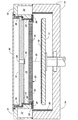
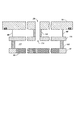
図1は、本発明の一実施形態により懸架されたシャワーヘッドを備えた真空チャンバーを示し、シャワーヘッドに固定されたハンガーが、チャンバー壁に固定された棚の上を自由にスライドするようにされる。新規な懸架体について説明する前に、真空チャンバーの他のコンポーネントを説明する。
1. Overview of Plasma Chamber FIG. 1 shows a vacuum chamber with a shower head suspended according to an embodiment of the present invention, in which a hanger fixed to the shower head slides freely on a shelf fixed to the chamber wall. To be done. Before describing the new suspension, the other components of the vacuum chamber are described.
真空チャンバーは、半導体又は他の電子デバイスをワークピース上に製造する一連のステップの中の1ステップである化学的プロセスをワークピース即ち基板10に受けさせるよう意図される。ワークピースは、チャック又はサセプタとも称されるワークピース支持体12によりチャンバー内に支持される。チャンバー内で処理されるワークピース10は、その一般例として、フラットパネルディスプレイが製造される長方形ガラス基板、又は集積回路が製造される円形半導体ウェアを含む。
The vacuum chamber is intended to cause the workpiece or
真空チャンバーは、チャンバー内部に対する真空包囲体を形成するハウジング又はチャンバー壁を有する。例示された実施形態では、チャンバーの側壁及び底壁が一体壁14として実施される。チャンバー壁の最上部には、ヒンジ式の蓋16と、ガス入口マニホールド最上壁18とが設けられる。個人は、蓋16を持ち上げることによりチャンバーの内部にアクセスすることができる。Oリング19(幾つかは図示せず)は、側壁14と蓋16とガス入口マニホールド最上壁18との間に真空シールを形成する。側壁及び底壁14、蓋16及びガス入口マニホールド最上壁18は、全て、チャンバー壁の部分であると考えられる。
The vacuum chamber has a housing or chamber wall that forms a vacuum enclosure for the interior of the chamber. In the illustrated embodiment, the sidewall and bottom wall of the chamber are implemented as a
本明細書内でチャンバーのコンポーネントの異なる側又は面を参照するときには、ワークピースに面した方の側又は面と、ワークピースから離れた方の側又は面を指すのに各々「前」及び「後」という語を使用する。例えば、ワークピース支持体12の上面は、ワークピース支持体の上面と称され、シャワーヘッド22の下面及び上面は、各々、シャワーヘッドの前面23及びシャワーヘッドの後面と称される。
When reference is made herein to different sides or faces of a chamber component, "front" and "front" respectively refer to the side or face facing the workpiece and the side or face away from the workpiece. The word “after” is used. For example, the upper surface of the
ワークピース上に半導体デバイス又は他の電子デバイスを製造するプロセスを遂行するときには、1つ以上のガスがガス入口マニホールドを経てチャンバー内に付与される。ガス入口マニホールドは、ガスが貫通してガス入口マニホールドに入って来るところのガス入口マニホールド最上壁18と、ガス入口マニホールドからプラズマチャンバーの内部へガスが貫通して流れるところのシャワーヘッド22(拡散器又はガス分配プレートとも称される)とを備えている。ガス入口マニホールドは、更に、最上壁18とシャワーヘッド22との間に延びるガスシールを形成するガスシール側壁とも称されるガス入口マニホールド側壁も備えている。ガス入口マニホールド最上壁、側壁及びシャワーヘッドは、集合的に、ガス入口マニホールドの内部領域即ち充満部26と称される容積部を包囲する。
When performing a process for manufacturing a semiconductor device or other electronic device on a workpiece, one or more gases are applied into the chamber via a gas inlet manifold. The gas inlet manifold has a gas inlet manifold
図示されていない外部ガス源は、ガス入口マニホールド最上壁18における少なくとも1つのガス入口オリフィス28にプロセスガスを供給し、これを経てプロセスガスはガス入口マニホールドの充満部26へ流れ込む。次いで、プロセスガスは、充満部から、シャワーヘッド22における1つ以上の、通常、数百又は数千のガス出口オリフィス30を経て、チャンバーの内部へ流れ込む。
An external gas source, not shown, supplies process gas to at least one
図1から図5の実施形態では、ガス入口マニホールドのガスシール側壁は、チャンバー蓋16の内面を覆う誘電体ライナー24で主として構成される。図6の別の実施形態では、ガス入口マニホールドの側壁は、以下に説明するハンガー70で主として構成される。図12から図14及び図17から図20の種々の実施形態では、柔軟性シート88がガス入口マニホールドのガスシール側壁として機能する。
In the embodiment of FIGS. 1-5, the gas seal sidewall of the gas inlet manifold is primarily comprised of a
ガス入口マニホールドの側壁は、充分な気密シールを与え、即ちガス漏れを充分に防ぎ、ガス入口オリフィス28を経て充満部へ流れ込むほとんどのガスが、ガス入口マニホールド側壁のギャップを経て漏れるのではなく、シャワーヘッドガス出口オリフィス30を経て流れることにより、真空チャンバーの内部に入り込むようにしなければならない。受け容れられる漏れの量は、ワークピースにおいて実行されるプロセスに依存するが、ほとんどのプロセスでは、漏れが10%未満でなければならない。即ち、ガス入口オリフィス28を経て充満部に入るガスのうち、ガス入口マニホールド側壁を経て漏れるのは、10%(1/10)未満でなければならず、従って、少なくとも90%のガスは、ガス出口オリフィス30を経て真空チャンバーへ付与されねばならない。最悪でも、ガス入口マニホールド側壁を経て漏れるのは、充満部に入るガスの40%以下でなければならない。
The side wall of the gas inlet manifold provides a sufficient hermetic seal, i.e. sufficiently prevents gas leakage, and most of the gas that flows into the filling through the
図示されていない従来の真空ポンプが、チャンバー内に希望の真空レベルを維持し、プロセスガス及び反応生成物をチャンバーから環状の排気スリット32を経て環状の排気充満部33へ、次いで、図示されていない排気チャンネルを経てポンプへと排気する。 A conventional vacuum pump, not shown, maintains the desired vacuum level in the chamber, and process gas and reaction products are passed from the chamber through the annular exhaust slit 32 to the annular exhaust fill 33 and then illustrated. Exhaust into the pump via no exhaust channel.
ここに示す好ましい実施形態では、シャワーヘッド22は、3cm厚みのアルミニウムプレートである。好ましくは、これは、チャンバー内に真空が形成されるときに大気圧のもとで著しく変形しないように充分な厚みでなければならない。
In the preferred embodiment shown here, the
このようなチャンバー内で実行されるある形式のワークピース製造プロセス、例えば、化学気相堆積(熱CVD)プロセスは、プラズマが存在しない状態で行われる。他の多くのプロセス、例えば、プラズマエンハンスト化学気相堆積(PECVD)やプラズマエッチングプロセスは、プラズマを必要とする。プラズマプロセスに使用するよう意図された真空チャンバーは、プラズマチャンバーと称される。 One type of workpiece manufacturing process performed in such a chamber, such as a chemical vapor deposition (thermal CVD) process, is performed in the absence of plasma. Many other processes, such as plasma enhanced chemical vapor deposition (PECVD) and plasma etching processes, require a plasma. A vacuum chamber intended for use in a plasma process is referred to as a plasma chamber.
一形式のプラズマチャンバーでは、チャンバー内の電極に接続された高周波(RF)電源でプラズマへ電力を容量性結合することによりチャンバー内にプラズマが発生され又は持続される。このようなプラズマチャンバーでは、シャワーヘッドは、電気的に接地されたチャンバー壁に接続されるか、或いはチャンバー壁から電気的に絶縁されてRF電源の非接地(RFホット)出力へ電気的に接続されることにより、電極の1つとして一般的に機能する。従って、通常、1キロワット程度の高レベルの高周波電力を導通するに充分な導電率及び信頼性の電気的接触をシャワーヘッドに与えることが重要である。 In one type of plasma chamber, plasma is generated or sustained in the chamber by capacitively coupling power to the plasma with a radio frequency (RF) power source connected to electrodes in the chamber. In such a plasma chamber, the showerhead is connected to an electrically grounded chamber wall or electrically isolated from the chamber wall and electrically connected to the ungrounded (RF hot) output of the RF power supply. Thus, it generally functions as one of the electrodes. It is therefore important to provide the showerhead with electrical contact with sufficient conductivity and reliability sufficient to conduct high-frequency power of the order of 1 kilowatt.
シャワーヘッドのガス出口オリフィス30は、プラズマチャンバー内のプラズマが、充満部26、即ちシャワーヘッド22とガス入口マニホールド最上壁18との間のガス入口マニホールドの内部領域に入るのを防止するために、その直径がプラズマダークスペースの巾より小さくなければならない。ダークスペースの巾、ひいては、ガス出口オリフィスの最適直径は、チャンバーの圧力と、チャンバー内で実行することが望まれる特定の半導体製造プロセスの他のパラメータとに依存する。或いは又、特に解離が困難な反応ガスを使用してプラズマプロセスを実行するために、前記チャン氏等の米国特許第4,854,263号に説明されたように、狭い入口及びフレアの付いた広い出口を有するオリフィスを使用することが望ましい。
The showerhead
又、ガス入口マニホールドは、ガス入口オリフィス28より直径が若干大きく且つ図示されないポストによりオリフィスの下に懸架された円盤34より成るガス入口偏向板も含むのが好ましい。この偏向板は、ガスが、ガス入口28から、シャワーヘッド中央の直接隣接ガス出口オリフィス30へまっすぐな経路に流れるのを阻止し、これにより、シャワーヘッドの中央及び周囲を通る各ガスの流量を等化する上で助けとなる。
The gas inlet manifold also preferably includes a gas inlet deflection plate that is slightly larger in diameter than the
ガス入口マニホールド最上壁及びシャワーヘッドがRFホットである用途では、これらRFホットのコンポーネントと、電気的に接地されたチャンバー蓋16との間に誘電体ライナー24、35が取り付けられる。ワークピース支持体12とシャワーヘッドとの間のチャンバー領域にプラズマを集中させるために、シャワーヘッド又はワークピース支持体の付近にあるチャンバーの他の金属面は、一般に、誘電体ライナーで覆われる。例えば、図1は、チャンバー蓋16の下面を覆う誘電体ライナー36と、チャンバー側壁14を覆う誘電体ライナー38とを示している。
In applications where the gas inlet manifold top wall and showerhead are RF hot,
カバー39は、一般に、チャンバー蓋16の上部に固定され、個人をRFホットの最上壁18又はシャワーヘッドに偶発的に接触することから保護する。カバー39は、ここに述べる他のチャンバーコンポーネントの機能に対して重要でないので、これ以上説明しない。
The
チャンバーのコンポーネントは、チャンバー内で実行されるべき半導体製造プロセスを汚染することない材料であって、プロセスガスによる腐食に耐える材料で構成されねばならない。アルミニウムは、以下に述べるように、Oリング並びに誘電体スペーサ及びライナー以外の全てのコンポーネントにとって好ましい材料である。 The components of the chamber must be made of a material that does not contaminate the semiconductor manufacturing process to be performed in the chamber and is resistant to corrosion by process gases. Aluminum is a preferred material for all components other than O-rings and dielectric spacers and liners, as described below.
従来のプラズマCVD及びエッチングチャンバーの設計及び運転は、参考としてここに全体の内容を援用する共通に譲渡された以下の米国特許に説明されている。98年12月1日にホワイト氏等に発行された米国特許第5,844,205号、及び89年8月8日にチャン氏等に発行された米国特許第4,854,263号。 The design and operation of conventional plasma CVD and etch chambers is described in the commonly assigned US patents, the entire contents of which are incorporated herein by reference. U.S. Pat. No. 5,844,205 issued to White et al. On Dec. 1, 1998, and U.S. Pat. No. 4,854,263 issued to Chang et al.
2.シャワーヘッドのためのスライド式支持体
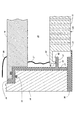
前記「発明の背景」のセクションで述べたように、チャンバー内で実行されているプロセスからの熱は、シャワーヘッド22の熱膨張を引き起こす。シャワーヘッドがチャンバー壁18に堅固に且つ非可撓的に取り付けられた場合には、このような熱膨張によりシャワーヘッドが曲がり、シャワーヘッドの前面即ち下面23が変形され、即ち下面の平坦さ又は曲率が変化し又は歪むことになる。
2. Slide Support for Shower Head As mentioned in the “Background of the Invention” section above, heat from the process being performed in the chamber causes the thermal expansion of the
図1から図3は、シャワーヘッドの周囲リム52をシャワーヘッド支持棚54に載せて、シャワーヘッドのリムが棚の上面を自由にスライドするようにシャワーヘッドを支持するという、この問題に対する1つの解決策を示す。従って、シャワーヘッドが温度の変化に応答して半径方向に膨張及び収縮するときには、シャワーヘッドのリムが棚を横切って各々外方及び内方にスライドする。この自由なスライドは、このような半径方向の熱膨張及び収縮に応答してシャワーヘッドにかかる応力を実質的に排除する。
FIGS. 1-3 show one approach to this problem, with the showerhead
棚54は、シャワーヘッドの重量を支持できる真空チャンバーのいかなる部分に固定することもできる。好ましくは、棚は、チャンバー壁18に直接的又は間接的に固定される。例示された好ましい実施形態では、棚は、蓋16の内面を覆う誘電体ライナー24の内方に突出する延長部である。
The
本特許出願が優先権を請求するところの米国特許第6,477,980号に説明されたように、シャワーヘッド22の周囲から、シャワーヘッドが直接的又は間接的に取り付けられる真空チャンバーの冷えたコンポーネント(例えば、チャンバー蓋16及びチャンバー側壁14)への熱伝達を最小にすることが望まれる。より詳細には、真空チャンバー内にシャワーヘッドを取り付けて支持する構造体は、好ましくは、シャワーヘッドとこのような冷えたチャンバーコンポーネントとの間に高い熱インピーダンスを介在させねばならない。このような熱伝達を最小にすることは、少なくとも2つの理由で効果的である。即ち、第1に、シャワーヘッドの温度を最大にして、ワークピースからシャワーヘッドへの熱ロスを最小にし、第2に、シャワーヘッドの周囲がシャワーヘッドの中央より速く熱を失う程度を最小にすることによりシャワーヘッドの下面の温度の空間的均一性を最大にする。
As described in US Pat. No. 6,477,980 to which this patent application claims priority, from the periphery of the
この原理を本発明に適用すると、支持棚54、又は支持棚とチャンバーの大きな冷えたコンポーネント(例えば、チャンバー蓋16及びチャンバー側壁14)との間のコンポーネントが、好ましくは、シャワーヘッドとこれらの冷えたコンポーネントとの間に高い熱インピーダンスを介在させねばならない。図3に例示された実施形態では、これは、誘電体ライナー24及びその一体的な支持棚54を熱伝導率の低い誘電体材料で製造して、誘電体ライナー及び支持棚がシャワーヘッドとチャンバー蓋16との間に高い熱インピーダンスを介在させることにより、達成される。
Applying this principle to the present invention, the
前記セクション1で述べたように、1つ以上のプロセスガスがガス入口マニホールドを経てチャンバーへ付与される。ガス入口マニホールドは、ガス入口マニホールド最上壁18と、シャワーヘッド22(拡散器又はガス分配プレートとも称される)と、ガス入口マニホールド最上壁、側壁及びシャワーヘッドが、集合的に、ガス入口マニホールドの内部領域即ち充満部26と称される容積部を包囲するように、最上壁18とシャワーヘッドとの間に延びるガスシール側壁と、を備えている。図1から図5の実施形態では、ガス入口マニホールドの側壁は、主として、誘電体ライナー24、支持棚54及びシャワーヘッドリム52で構成される。
As described in section 1 above, one or more process gases are applied to the chamber via the gas inlet manifold. The gas inlet manifold includes a gas inlet manifold
又、前記セクション1で述べたように、ガス入口マニホールドのガスシール側壁は、ガス入口オリフィス28を経て充満部に流れ込むガスのほとんどが、ガス入口マニホールドの側壁のギャップを経て漏れるのではなく、シャワーヘッドのガス出口オリフィス30を経て流れることにより、真空チャンバーの内部に入るように、充分な気密シールを与えねばならない。従って、シャワーヘッドリム52及びシャワーヘッド支持棚54は、いずれの1つのコンポーネント内にも又は隣接コンポーネント間にも、プロセスガスの著しい部分が充満部から漏れ得るような著しく大きなギャップを有してはならない。好ましくは、ガス入口オリフィス28を経て充満部に入るガスのうち、ガス入口マニホールド側壁を経て漏れるのは、10%(1/10)未満でなければならず、従って、少なくとも90%のガスは、ガス出口オリフィス30を経て真空チャンバーへ付与されねばならない。それ故、前記ギャップの合成断面積(側壁ギャップ面積)は、好ましくは、シャワーヘッドの出口オリフィスの最も狭い部分の合成断面積(シャワーヘッドオリフィス面積)の10%(1/10)未満でなければならない。最悪でも、側壁ギャップ面積は、シャワーヘッドオリフィス面積の40%未満でなければならない。
Also, as described in section 1 above, the gas seal side wall of the gas inlet manifold has a shower that does not leak most of the gas that flows into the filling through the
リム及び棚の両方は、1つの連続する部片として製造することもできるし、或いは充分な気密シールを形成するように密接に当接する多数の部片として製造することもできる。例えば、図3は、シャワーヘッドリム52が連続部片である一方、支持棚54が突出する誘電体ライナー24が4つの個別の部片を有し、長方形のチャンバー蓋16の4つの内面を各々覆うところを示している。シャワーヘッドのリム52は、シャワーヘッドの一体的部分として加工することもできるし、又は中央が開いた長方形フレームで、その周囲付近でシャワーヘッドに固定されるような長方形フレームでもよい。
Both rims and shelves can be manufactured as one continuous piece or as multiple pieces in close contact to form a sufficient hermetic seal. For example, FIG. 3 shows that the
図4は、長方形ではなく円筒状のシャワーヘッド22にこの設計をいかに適応できるかを示す。この実施形態では、シャワーヘッドリム52、シャワーヘッド支持棚54及び誘電体ライナー24は、全て、円筒状で、シャワーヘッド22と同心的である。
FIG. 4 shows how this design can be applied to a
信頼性のある高導電率のRF電気接続をシャワーヘッドに与えるために、図2に示すように、RF電気ケーブル56(上部ケーブルと称される)をガス入口マニホールド最上壁18に電気的に接続することができると共に、第2のRFケーブル57(下部ケーブルと称される)を最上壁18とシャワーヘッドとの間に直結することができる。
To provide a reliable, high conductivity RF electrical connection to the showerhead, an RF electrical cable 56 (referred to as the top cable) is electrically connected to the gas inlet manifold
シャワーヘッドリム52とシャワーヘッド支持棚54との間のスライド接触における摩擦が接触面を磨耗して粒子を形成する。チャンバー蓋16の下面を覆う誘電体ライナー36は、このような粒子のほとんど又は全部を捕獲してそれらがワークピース10に落下するのを防止するように棚54の下に少なくとも部分的に延びるのが好ましい。任意であるが、シャワーヘッドは、誘電体ライナー36で捕え損なうことのある粒子を捕獲するように第1のリム52の下に配置された第2の周囲リム即ちトラフ58を含むことができる。
Friction in sliding contact between the
シャワーヘッドリム52の下面とシャワーヘッド支持棚54の上面との間の摩擦及び磨耗を減少するために、滑らかな低摩擦滑走体即ちベアリング61をこれらの面のいずれか又は両方に取り付けることができる。例えば、滑走体は、これら表面の1つに埋め込まれたロッド又は1つ以上のボールである。任意であるが、この滑走体は、このような面内のソケットであってその中で滑走体を自由に転がすことのできるソケットに嵌合させることもできる。
To reduce friction and wear between the lower surface of the
図5は、図2の設計の変形態様を示すもので、ここでは、シャワーヘッド支持棚54の内端が、上方に延びるリップ62を有し、棚とシャワーヘッドリム52との間の磨耗により発生された粒子を棚により捕獲して、ワークピースへ落下しないよう確保する。棚のリップ62のための間隙を与えるために、シャワーヘッドリム52の外端は、周囲リップ64を有し、これは、棚リップ62の高さより少なくとも若干大きな長さで下方に延びて、シャワーヘッドリップ64の下端がシャワーヘッドリム52と支持棚54との間の唯一の接触点となるようにしなければならない。シャワーヘッドリップ64は、支持棚リップ62の半径方向外方にある支持棚52の上方を向いた面に載せねばならない。好ましくは、上述した滑走体61がシャワーヘッドリップ64の下面に取り付けられる。
FIG. 5 shows a variation of the design of FIG. 2 in which the inner end of the
シャワーヘッドが外方にスライドしたときに支持棚の立ち上がったリップ62がシャワーヘッドの側部に当たって粒子を発生するのを防止するために、シャワーヘッドリム52は、好ましくは、その半径方向の巾が支持棚の半径方向の巾より大きくなければならない。より詳細には、シャワーヘッドリムのリップ64は、このシャワーヘッドリップ64がスライドする支持棚上面の半径方向巾より大きな長さで、シャワーヘッドの側部の半径方向外方に離間されねばならない。
To prevent the rising
3.ハンガーでシャワーヘッド支持棚を上壁から懸架する
図6は、図5の実施形態と同一であるが、シャワーヘッド支持棚54が誘電体ライナー24に固定されない別の実施形態を示す。むしろ、シャワーヘッド支持棚54は、ガス入口マニホールド最上壁18からハンガー70により懸架されている。図6の実施形態は、図1から図5の実施形態と同様に、シャワーヘッドリム52を、それが載せられた支持棚54の面にスライドさせるのを許容することにより、シャワーヘッドの半径方向熱膨張を受け容れる。以下に述べる相違点を除くと、図1から図5の実施形態を参照して説明した全ての変形及び設計事項が図6の実施形態にも適用される。
3. Suspending the shower head support shelf from the top wall with a hanger FIG. 6 shows another embodiment that is identical to the embodiment of FIG. 5 but in which the shower
最上壁18、ハンガー70、支持棚54、滑走体61及びシャワーヘッドリム52の全部がアルミニウム又は他の金属のような導電性材料で構成される場合には、これらコンポーネントは、最上壁18をシャワーヘッド22に電気的に接続し、上壁からシャワーヘッドへRF電力を確実に導通させる。支持棚に載せられるシャワーヘッドの重みは、シャワーヘッドリムと支持棚との間の接触領域において信頼性のある高導電率の電気的接続を達成する上で助けとなる。それ故、図2の実施形態のように、上壁とシャワーヘッドとの間を個別の電気ケーブルで接続する必要はないであろう。
If the
本特許出願が優先権を請求するところの米国特許第6,477,980号に説明された柔軟性懸架体とは異なり、シャワーヘッドリムが支持棚を自由にスライドするので、ハンガー70が柔軟性である必要はない。ハンガー70は、最上壁18と一緒に一体的なモノリシック部片として製造されてもよいし、又は最上壁18にボルト固定又は他の仕方で固定できる個別の部片でもよい。
Unlike the flexible suspension described in US Pat. No. 6,477,980 to which this patent application claims priority, the
前記セクション2に説明されたように、ガス入口マニホールドは、好ましくは、プロセスガスの過剰な部分が充満部26から漏れるのを防止するに充分な気密シールを与えねばならない。上述したように、漏れの量は、ワークピースに対して実行されるプロセスに大きく依存するが、ほぼ全ての用途では、漏れの量が、シャワーヘッドガス出口オリフィス30を通るガス流の40%未満、好ましくは10%未満、でなければならない。ハンガー70でシャワーヘッド支持棚をガス入口マニホールド最上壁18に取り付ける図6の実施形態では、ハンガー70が、シャワーヘッド支持棚54及びシャワーヘッドリム52と協働するガス入口マニホールドの側壁として機能する。それ故、これらコンポーネントの各々は、好ましくは、いずれの1つのコンポーネント内でも又は隣接コンポーネント間にも、プロセスガスの前記部分より多くが充満部から漏れ得るような実質的なギャップを有してはならない。これらコンポーネントは、どれも、1つの連続する部片として製造することもできるし、或いは充分な気密シールを形成するように密接に当接する多数の部片として製造することもできる。これら製造解決策の実施例は、前記セクション2に述べた。
As described in Section 2 above, the gas inlet manifold should preferably provide a sufficient hermetic seal to prevent excess portions of the process gas from leaking from the
図1から図5の実施形態の説明で述べたように、真空チャンバー内にシャワーヘッドを取り付けて支持する構造体は、好ましくは、シャワーヘッドとこのような冷えたチャンバーコンポーネントとの間に高い熱インピーダンスを介在させねばならない。ハンガー70を有する図5の実施形態では、これは、シャワーヘッドと最上壁18との間にハンガーが介在させる熱インピーダンスを最大にすることにより達成できる。このような熱インピーダンスは、ハンガーを非常に薄く作るか、或いはプラズマチャンバーの内部に使用するのに適したほとんどの他の電気導体より熱伝導率の低いステンレススチールのような低熱伝導率の材料でハンガーを製造することにより、最大にすることができる。1つの好ましい実施形態では、前者の解決策が使用され、即ち希望の低い熱伝導率を有するに充分なほど薄くハンガーが作られる。厚みが3mm以下、好ましくは1mm以下のアルミニウムシートでハンガー70を製造することが推奨される。
As described in the description of the embodiment of FIGS. 1-5, the structure for mounting and supporting the showerhead in the vacuum chamber preferably has a high heat between the showerhead and such a chilled chamber component. Impedance must be interposed. In the embodiment of FIG. 5 with
4.ピンがスロット内をスライドするハンガー
図7から図9は、複数のハンガー80がシャワーヘッド及び最上壁18にピン81により取り付けられ、ピン81はスロット82内をスライドし、半径方向のシャワーヘッドの熱膨張を受け容れるようにハンガーが半径方向にスライドするのを許容するような懸架体により、シャワーヘッド22がガス入口マニホールド最上壁18から懸架された実施形態を示す。
4). FIGS. 7 to 9 show that a plurality of
シャワーヘッド22の上面は、図7に示すように、シャワーヘッドの周囲付近で周辺方向に分布した位置に複数のスロット82を有する。各スロットの最も長い寸法(長さ)は、シャワーヘッドの長手軸55(図1及び7を参照)に対して半径方向に延びている。これらスロットは、シャワーヘッドの本体に製造できるが、図7から図9に示すように、シャワーヘッドの外方に延びるリム78にスロットを製造するのが容易である。
As shown in FIG. 7, the upper surface of the
ここに示す長方形のシャワーヘッドでは、シャワーヘッドは、その上面の4つのコーナー各々の付近に1つのスロットを有すると共に、4つのコーナー各々の間の中間に1つのスロットを有する。或いは又、シャワーヘッドは、それより多数又は少数のスロットを含むこともでき、例えば、コーナー付近に4つのスロットだけを含むか、コーナー間の中間に4つのスロットだけを含むか、シャワーヘッドの上面の対向する側部に2つのスロットだけを含むか、又は周囲方向に分布した3つのスロットだけを含むことができる。 In the rectangular showerhead shown here, the showerhead has one slot near each of the four corners on its top surface and one slot in the middle between each of the four corners. Alternatively, the showerhead can include more or fewer slots, for example, including only four slots near the corners, only four slots in the middle between corners, or the top surface of the showerhead. May include only two slots on opposite sides of the or only three slots distributed in the circumferential direction.
シャワーヘッドのスロット82ごとに、対応するハンガー80には、そのスロットを通して延びるピン81が設けられる。ピン81の下端から横方向に延びる肩部83は、スロットの横巾、即ちシャワーヘッドの方位又は周囲に平行なスロットの寸法より広い。従って、肩部83は、図9に示すように、スロットを横方向に境界定めするシャワーヘッドの部分85の下面に係合して支持する。(スロットを横方向に境界定めするシャワーヘッドの部分は、スロット側壁85と称する。)
各ピン81及びその肩部83は、円形又は長方形断面のような断面形状をもつことができる。例えば、各ピンは、ねじ切りされたボルトとして実施することができ、各ピンの肩部は、ボルトの頭でよい。
For each
Each
上述したようにシャワーヘッドに直接係合して支持するハンガー80は、ハンガーの第1又は最下「層」と称される。考えられる1つの実施形態では、懸架体は、ハンガーの単一層しか含まず、この場合、各ハンガーは、シャワーヘッド22と最上壁18との間に延びるに充分なほど背が高くなければならない。
The
より詳細には、懸架体は、図8及び9に示すようにハンガー80の多数の層を含み、これら層の数を整数Nとすれば、各ハンガーの高さは、おおよそ、シャワーヘッドと上壁との間の距離をNで除算したものとなる。ここに示す実施形態では、シャワーヘッドと上壁との間にハンガーの2つの層があり、即ちN=2である。
More specifically, the suspension includes a number of layers of
各ハンガー80の上面は、シャワーヘッドにおける対応スロットと同じ方向のスロット82を有する。より詳細には、各ハンガーのスロットは、その最も長い寸法がシャワーヘッドの半径に平行に向けられ、即ちシャワーヘッドの長手軸55(図1)に垂直に向けられる。スロット82の真下でそれに隣接して、各ハンガーはグルーブ84も有し、このグルーブは、スロットを通して延びるピン81の肩部83より巾が広く、ピンがスロット内をスライドする間に肩部83をスライドできるところの空洞を形成する。
The upper surface of each
ガス入口マニホールド最上壁18の下面は、最も上の層のハンガー80の数に等しい多数の下方に突出するピン81を含む。これらピン81は、上壁の周囲付近で周囲方向に分布した位置に配置され、最上壁18の個別のピンが最も上の層の各ハンガーに係合するようにされる。又、各ハンガーの下面も、下方に突出するピン81を有する。上壁の各ピン81及びハンガーの各ピン81は、上述した肩部83を有する。
The lower surface of the gas inlet manifold
最上壁18の各ピンは、それに対応するハンガー80のスロット82を通過する。各ハンガーのスロットは、シャワーヘッドの各スロットの側壁85と同様に、側壁85を有するものとして説明する。即ち、スロット82を横方に境界定めし且つグルーブ84に垂直にオーバーハングするハンガーの部分を、スロット側壁85と称する。各ハンガーのスロット側壁85は、スロットを通過するピン81の肩部83に載せられる。というのは、ピンの肩部は、図9に示すようにスロットの横断巾より広いからである。従って、ピン及び肩部はスロットの側壁85を支持し、ひいては、それが一部分であるところのハンガーを支持する。
Each pin of the
同様に、ハンガーの層が2つ以上ある場合には、最下層の上の1つ以上の層における各ハンガーが、その下のハンガーを支持する。というのは、このような各ハンガーは、その真下のハンガーのスロットを通過するピンを有し、且つ各ピンは、その真下のハンガーの対応スロット82の横断巾より広い肩部83を有するからである。
Similarly, if there are two or more layers of hangers, each hanger in one or more layers above the bottom layer supports the hangers below it. This is because each such hanger has a pin that passes through the slot of the hanger just below it, and each pin has a
従って、最下層のハンガーの肩部及びピンは、集合的に、シャワーヘッドの全重量を支持する。上壁の肩部及びピンは、集合的に、ハンガーの最上層の重量を支持する。最下層以外のハンガーの各層の肩部及びピンは、集合的に、その真下のハンガーの次の層の重量を支持する。 Thus, the shoulders and pins of the lowermost hanger collectively support the full weight of the showerhead. The upper wall shoulders and pins collectively support the weight of the top layer of the hanger. The shoulders and pins of each layer of the hanger other than the bottom layer collectively support the weight of the next layer of the hanger just below it.
ピン及びスロットは、各ハンガーが下ではシャワーヘッド及び上ではガス入口マニホールド最上壁に対して半径方向にスライドするのを許容するので、シャワーヘッドは、温度変化に応答して自由に膨張及び収縮することができる。 The pins and slots allow each hanger to slide radially against the showerhead and above the top wall of the gas inlet manifold so that the showerhead expands and contracts freely in response to temperature changes. be able to.
図10は、シャワーヘッドリム78と、それが載せられたピンの肩部との間の磨耗により発生される粒子を捕獲することが望まれる場合に、(1)スロット82の下のグルーブ84、及び(2)グルーブの下の内実部分79を含むようにリムを変更できることを示している。
FIG. 10 illustrates that when it is desired to capture particles generated by wear between the
図11は、図7から10に示す実施形態に対してピン及びスロットが逆転された別の実施形態を示すもので、ここでは、各ピン81がハンガー80又はその上の最上壁18のスロット82へと上方に延びると共に、各ピンの肩部83の下面が、ハンガー又はその上の上壁のスロット82を横方向に境界定めするスロット側壁85に載せられてそれにより支持される。しかしながら、各ピン81がスロット82へと下方に延びる実施形態が好ましい。というのは、上方を向いたグルーブ84が、肩部83とスロットの側壁85との間の磨耗により発生される粒子を捕獲して、このような粒子がワークピースへ落下しないようにできるからである。
FIG. 11 shows another embodiment in which the pins and slots are reversed relative to the embodiment shown in FIGS. 7-10, where each
前記セクション1に述べたように、1つ以上のプロセスガスがガス入口マニホールドを経てチャンバーに付与される。ガス入口マニホールドは、ガス入口マニホールド最上壁18と、シャワーヘッド22(拡散器又はガス分配プレートとも称される)と、これら最上壁18とシャワーヘッドとの間に延びるガス入口マニホールド側壁とを備え、ガス入口マニホールドの側壁、上壁及びシャワーヘッドは、集合的に、ガス入口マニホールドの内部領域即ち充満部26と称される容積部を包囲する。
As described in section 1 above, one or more process gases are applied to the chamber via the gas inlet manifold. The gas inlet manifold includes a gas inlet manifold
図8から図11の各実施形態において、各ハンガー80の横断巾は、ハンガー内のグルーブ84の横断巾より著しく大きい必要はない。(横断巾とは、ハンガーがスライドする方向に垂直な方向におけるハンガーの巾で、図8において左から右へのハンガーの巾を意味する。)従って、ハンガー80は、ガス入口マニホールドのための側部シールとして機能するに充分な広さでなくてもよい。即ち、隣接ハンガー間に大きな横断間隔がある場合には、ハンガーがガス入口マニホールドのためのガスシール側壁を形成しない。
In the embodiments of FIGS. 8-11, the width of each
この場合には、ガス入口マニホールドのためのガスシール側壁は、好ましくは、ガス入口マニホールド最上壁18とシャワーヘッド22との間に1つ以上のガスシール部材88を取り付けることにより形成されねばならない。このガス入口マニホールド側壁88は、最上壁18のガス入口オリフィス28とシャワーヘッドのガス出口オリフィス30との間に延びる容積部即ち充満部26を包囲しなければならない。このガス入口マニホールド側壁88は、半径方向のシャワーヘッドの熱膨張を受け容れるに充分なほど柔軟性でなければならない。
In this case, the gas seal sidewall for the gas inlet manifold should preferably be formed by attaching one or more
図12は、ガス入口マニホールド最上壁18の周囲とシャワーヘッド22のリム78とに取り付けられてそれらの間に延びる1つ以上の柔軟性シート又は膜88で構成されたガス入口マニホールドのための1つの適当なガスシール側壁を示す。シャワーヘッドの長手軸55の方向におけるシート又は膜88の長さ又は高さは、このシートがシャワーヘッドの熱膨張を受け容れるに充分なたるみ又はゆるみをもつように最上壁18とシャワーヘッドとの間の距離をまたぐために必要以上に大きくなければならない。ここに示す長方形のシャワーヘッドの場合には、ガスシール88は、最上壁及びシャワーヘッドの全周にわたって延びる単一のシートでもよいし、或いは最上壁及びシャワーヘッドの4つの辺に各々取り付けられる4つの別々のシートを含んでもよい。
FIG. 12 shows one for a gas inlet manifold constructed with one or more flexible sheets or
図13及び図14は、柔軟性シート又は膜88の下端が、ハンガー80の半径方向内方で且つガス出口オリフィス30の半径方向外方の面に沿ってシャワーヘッド22に取り付けられる別の実施形態を示す。
FIGS. 13 and 14 show another embodiment in which the lower end of the flexible sheet or
シャワーヘッドの重量は、シート88ではなくハンガー80により完全に支持される。それ故、シート88は、重たいシャワーヘッドを支持するに充分な強さではなく、入口マニホールドに供給されるガスとチャンバーの真空との間の圧力差に耐えるに充分な強さであればよい。従って、シートは、非常に柔軟であるに充分な薄い材料で構成することができる。
The showerhead weight is fully supported by the
図15は、ハンガー80がガス入口マニホールドのガスシール側壁として機能し、付加的な柔軟性シール88の必要性を排除する別の実施形態を示している。これは、ハンガー80の各々が充分に大きな横断巾を有し、隣接するハンガーの横端を互いに充分に接近させて、充満部26内のプロセスガスの著しい部分がシャワーヘッドのガス出口オリフィス30を経て流れるのではなくハンガー間のギャップを経て漏れるのを防止することを必要とする。
FIG. 15 shows another embodiment in which the
前記セクション1で述べたように、受け容れられる漏れの量は、ワークピースに対して実行されるプロセスに依存するが、ほとんどのプロセスでは、漏れが10%未満でなければならない。即ち、ガス入口オリフィス28を経て充満部26に入るガスのうち、ガス入口マニホールド側壁を経て漏れるのは、10%(1/10)未満でなければならず、従って、少なくとも90%のガスは、ガス出口オリフィス30を経て真空チャンバーへ付与されねばならない。最悪でも、ガス入口マニホールド側壁を経て漏れるのは、充満部に入るガスの40%以下でなければならない。
As stated in section 1 above, the amount of leakage that is accepted depends on the process being performed on the workpiece, but for most processes the leakage must be less than 10%. That is, less than 10% (1/10) of the gas entering the
それ故、好ましくは、ハンガーの横断巾が充分大きく、且つハンガー間のギャップが充分小さくて、ハンガー間のギャップの合成断面積(側壁ギャップ面積)が、シャワーヘッドの出口オリフィスの最も狭い部分の合成断面積(シャワーヘッドオリフィス面積)の10%(1/10)未満でなければならない。最悪でも、側壁ギャップ面積は、シャワーヘッドオリフィス面積の40%未満でなければならない。 Therefore, it is preferable that the cross-sectional width of the hanger is sufficiently large and the gap between the hangers is sufficiently small so that the combined cross-sectional area (side wall gap area) of the gap between the hangers is the combined portion of the narrowest portion of the outlet orifice of the showerhead. It must be less than 10% (1/10) of the cross-sectional area (shower head orifice area). At worst, the sidewall gap area should be less than 40% of the showerhead orifice area.
ハンガーの隣接端が、隣接ハンガー間のギャップを橋絡する柔軟性シート又はベロー(図示せず)に取り付けられる場合には、隣接ハンガーの横端間のギャップを通るガス漏れを更に減少することができる。 If the adjacent ends of the hangers are attached to a flexible sheet or bellows (not shown) that bridges the gap between adjacent hangers, gas leakage through the gap between the adjacent ends of the adjacent hangers may be further reduced. it can.
図16は、ハンガー80が、充分に巾の広い横方向延長部89を含み、各対の隣接ハンガーの横方向延長部が重畳するような別の設計を示す。各対の重畳する延長部は、互いに充分接近離間されて、それらの間のギャップが充満部からのガスの漏れを防ぎ、充満部に入るガスのうち、シャワーヘッドのガス出口オリフィス30を経て流れるのではなく全ての前記ギャップを経て漏れるのが40%(2/5)を越えるのを防止し、好ましくは、10%(1/10)未満にしなければならない。或いは又、ハンガー間のギャップの合成断面積は、シャワーヘッドの出口オリフィスの最も狭い部分の合成断面積の40%(2/5)未満でなければならず、好ましくは、10%(1/10)未満でなければならない。
FIG. 16 shows another design in which the
5.ワイヤ懸架体
図17及び図18は、シャワーヘッド22が3つ以上の柔軟なワイヤ86により懸架される実施形態を示す。各ワイヤの上端は、ガス入口マニホールド最上壁18の周囲付近のポイントに取り付けられ、一方、各ワイヤの下端は、シャワーヘッドの周囲付近のポイントに取り付けられる。上部取り付けポイントは、最上壁18において周囲方向に分布され、下部取り付けポイントは、シャワーヘッドにおいて周囲方向に分布される。
5. Wire Suspension FIGS. 17 and 18 show an embodiment in which the
ここに示す好ましい実施形態では、シャワーヘッド及びガス入口マニホールド最上壁18は長方形であり、ワイヤの本数は4であり、ワイヤの取り付けポイントは、シャワーヘッド及びガス入口マニホールド最上壁の4つのコーナー付近である。(4本のワイヤ及びそれらの取り付けポイントをより明確に示すために、図17及び図18は、4本のワイヤ、シャワーヘッド、ガス入口マニホールド最上壁、及び以下に述べるガスシール88以外の全てのコンポーネントを省略している。)
ワイヤが柔軟であるので、シャワーヘッドは、温度変化に応答して、応力を生じることなく、自由に膨張及び収縮する。
In the preferred embodiment shown here, the showerhead and gas inlet manifold
Because the wire is flexible, the showerhead expands and contracts freely in response to temperature changes without causing stress.
好ましくは、ワイヤは、ガス入口マニホールド最上壁からシャワーヘッドへRF電力を導通するよう機能できるように導電性金属で構成される。 Preferably, the wire is constructed of a conductive metal so that it can function to conduct RF power from the top wall of the gas inlet manifold to the showerhead.
ワイヤの直径は、シャワーヘッドの横断巾の僅かな部分に過ぎないので、ワイヤは、ガス入口マニホールドの充満部即ち内部領域26を包囲する側壁として機能することができない。従って、ガス入口マニホールドの側部を包囲するために個別のガスシール88を設けねばならない。このガスシールは、シャワーヘッドの熱膨張を受け容れるために充分に柔軟でなければならない。
Since the diameter of the wire is only a small part of the showerhead's transverse width, the wire cannot serve as a side wall surrounding the full or
前記セクション4(図12から14)で述べたガスシール88の設計は、いずれも、ワイヤ懸架体86と組み合わせて使用するのに等しく適している。図17及び図18は、図12に示したものと同様の周囲シール88を示す。図19は、図13及び14に示すシール88と同様に、ワイヤ86の半径方向内方で且つガス出口オリフィス30の半径方向外方にある面に沿ってシャワーヘッド22に取り付けられた別のシール88を示す。
Any of the
6.関節ジョイントを伴う懸架ロッド
図20は、図19と同様であるが、シャワーヘッドがワイヤではなくロッド90により懸架された実施形態を示す。各ロッドの上端及び下端は、関節ジョイント91によりシャワーヘッド及びガス入口マニホールド最上壁に各々取り付けられる。関節ジョイントは、ロッドが柔軟である必要性を排除し、従って、ロッドは、太くて堅固なものでよい。
6). Suspension Rod with Articulated Joint FIG. 20 is similar to FIG. 19 but shows an embodiment where the showerhead is suspended by a
関節ジョイントは、従来のボール及びソケットジョイントのように、ロッドがジョイントで枢着回転するのを許容する従来設計のものでよい。ボール及びソケットジョイントの低廉な近似は、図20に示すように、ボールに代わってショルダースクリューの頭を、そしてソケットに代わってホール又はスロットを使用することができる。スロットは、横断又は半径方向に細長くして、ロッドが枢着回転に加えて横断又は半径方向にスライドするのを許容する。 The joint joint may be of a conventional design that allows the rod to pivot about the joint, such as a conventional ball and socket joint. An inexpensive approximation of a ball and socket joint can use a shoulder screw head in place of the ball and a hole or slot in place of the socket, as shown in FIG. The slot is elongated transversely or radially to allow the rod to slide transversely or radially in addition to pivoting rotation.
「ワイヤ懸架体」と題するセクション5で説明したように、ガス入口マニホールドの側部に対するガスシールを与えるために、シート88を設けねばならない。
As described in
7.高い熱膨張係数をもつ支持体への堅固な取り付け
図21及び22は、柔軟性又はスライド式コンポーネントを必要とせずにシャワーヘッドを堅固に取り付けるのを許し、しかも、半径方向の熱膨張及び収縮を受けるときにシャワーヘッドにかかる応力を緩和する別の設計を示す。この設計の独特の要素は、シャワーヘッド22の材料より高い熱膨張係数を有する材料で構成されたシャワーヘッド支持部材100である。シャワーヘッドは、熱膨張係数の高い支持部材100から堅固に懸架される。懸架体は少なくとも1つのスペーサ102を含み、各スペーサは、その上端が支持部材100の周囲付近に取り付けられ、又、その下端がシャワーヘッド22の周囲付近に取り付けられる。
7). Rigid attachment to a support with a high coefficient of thermal expansion FIGS. 21 and 22 allow a showerhead to be rigidly attached without the need for flexible or sliding components, yet provide radial thermal expansion and contraction. Figure 2 shows another design that relieves stress on the showerhead when subjected. A unique element of this design is a
シャワーヘッド支持部材100、スペーサ102及びシャワーヘッド22は、集合的に、プロセスガスがシャワーヘッドガス出口オリフィス30を経て真空チャンバーの内部へ付与される前に流れ込むところの容積部即ち充満部101を包囲する。これらコンポーネントは、充満部の周りに実質的な気密シールを与え、従って、シャワーヘッド出口オリフィス30を通過せずに充満部から真空チャンバーの内部へ漏れるガスの量が無視できる程度より多くならないようにしなければならない。
The
シャワーヘッドが円形である場合には、スペーサ102が円筒状であるのが好ましい。例示された実施形態では、シャワーヘッドが長方形であり、スペーサ102が、開いた中央部を取り巻く長方形フレームである。或いは又、多数のスペーサ102をシャワーヘッド22の周辺部に周囲方向に分布させることもできるが、このときには、隣接スペーサ間にガスシールを設けなければならない。
When the shower head is circular, the
ガスコンジット106は、その上端が真空チャンバー最上壁18に取り付けられ、そこで、ガス入口オリフィス28に結合される。ガスコンジット106の下端は、シャワーヘッド支持部材100に取り付けられ、そこで、シャワーヘッド支持部材の少なくとも1つのガスオリフィス104に結合される。従って、ガスコンジット106は、プロセスガスが、ガス入口オリフィス28から、シャワーヘッド支持部材のガスオリフィス104を経て、充満部101を経て、次いで、シャワーヘッドのガス出口オリフィス30を経て流れるための流路を形成する。
The
この設計の動作原理は、次の通りである。充満部101内のプロセスガスによる熱伝導及び対流は、シャワーヘッド22とシャワーヘッド支持部材100との間に熱を伝達するように機能する。それ故、シャワーヘッドの温度が上下するときに、シャワーヘッド支持部材100の温度が上下する。又、スペーサ102も、シャワーヘッドと支持部材との間に熱を伝達することができる。ガス及びスペーサによる熱伝達は、効率が100%未満であるために、支持部材は、一般に、シャワーヘッドより冷たくなる。それ故、支持部材及びシャワーヘッドが同じ熱膨張係数を有する場合には、支持部材が、チャンバー内で実行されているプロセスからの熱に応答してシャワーヘッドほど膨張及び収縮しない。
The operating principle of this design is as follows. The heat conduction and convection by the process gas in the filling
しかしながら、本発明によれば、支持部材がシャワーヘッドとほぼ同じ量だけ半径方向に膨張するように、支持部材100の熱膨張係数は、シャワーヘッドの熱膨張係数を最適な量だけ越えねばならない。換言すれば、支持部材100は、これが高い温度に応答してシャワーヘッドの半径方向膨張にほぼ等しい量だけ半径方向に膨張するように、熱膨張係数がシャワーヘッドを最適な量だけ越える材料で構成されねばならない。支持部材の最適な熱膨張係数は、支持部材100を異なる材料で製造し、チャンバー内で実行されるプロセス中におそらく遭遇する温度変化に応答してシャワーヘッドとほぼ同じ量だけ支持部材を膨張及び収縮させる材料を選択することにより、実験で決定することができる。
However, according to the present invention, the thermal expansion coefficient of the
ガスコンジット106は、シャワーヘッド支持部材100にその中央付近で取り付けられるので、そのポイントにおける支持部材の半径方向膨張は、その周囲付近での半径方向膨張に比して無視できるものである。それ故、ガスコンジットは、シャワーヘッド支持部材に堅固に取り付けることができる。1つの意図された実施形態では、ガスコンジットは、シャワーヘッド支持部材及びシャワーヘッドの全重量を支持する。より好ましくは、支持部材100の周囲と最上壁18との間に前記セクション2から6で述べた柔軟性又はスライド式懸架体を取り付けることにより、ヒーター及びシャワーヘッドの重量に対する付加的な支持を与えることができる。或いは又、「関連出願へのクロスレファレンス」という見出しで本特許明細書の初めに示した、本出願が優先権を請求するところの2つの以前の特許出願に説明された懸架設計のものを、支持部材100と最上壁18との間に取り付けることもできる。図21及び図22に示す好ましい実施形態では、このような支持は、4本の柔軟性ワイヤ86により与えられ、これらワイヤは、セクション5で述べた図17から図19の実施形態のように、シャワーヘッドの4つのコーナーに各々取り付けられる。
Since the
ガスコンジット106、支持部材100及びスペーサ102は、それらが全て導電性材料で構成された場合には、チャンバーの最上壁18からシャワーヘッドへRF電力を導通するように機能することができる。これらコンポーネントの各々は堅固に取り付けできるので、上述した取り付けポイントの各々は、優れたRF電気的コンダクタンスを与えるように容易に実施することができる。
The
8.シャワーヘッド後方のヒーター
上述した種々の懸架設計は、全シャワーヘッドの温度の上下に応答したシャワーヘッドの半径方向の膨張及び収縮による応力を防止することが意図される。これまでの設計で完全に対処されていない付加的な問題は、シャワーヘッドの前面(下面)が一般にシャワーヘッドの後面(上面)より高温になることである。というのは、前面が、チャンバー内の主熱源、即ち(1)ワークピース10を加熱するために通常ヒーターを含むワークピース支持体12、及び(2)プラズマプロセスの場合には、シャワーヘッドとワークピース支持体との間の領域のプラズマ、を向いているからである。これに対して、シャワーヘッドの後面は、ガス入口マニホールド最上壁18のように、シャワーヘッドより通常冷たい表面に露出される。
8). Heaters behind the showerhead The various suspension designs described above are intended to prevent stress due to the radial expansion and contraction of the showerhead in response to increasing and decreasing temperature of the entire showerhead. An additional problem that has not been fully addressed by previous designs is that the front surface (lower surface) of the showerhead is generally hotter than the rear surface (upper surface) of the showerhead. This is because the front face is the main heat source in the chamber, (1) the
シャワーヘッドの前面が後面より高温になると、前面は後面より膨張して、シャワーヘッドを熱源に向って外方に曲げさせる。即ち、前面はより凸状になる。「発明の背景」で述べたように、シャワーヘッドの前面の輪郭(平坦さ又は曲率)に対する変化は、望ましくない。というのは、ワークピースに対して行なわれているプロセスの空間均一性を損なうことになるからである。 When the front surface of the shower head becomes hotter than the rear surface, the front surface expands from the rear surface, causing the shower head to bend outward toward the heat source. That is, the front surface becomes more convex. As mentioned in “Background of the Invention”, changes to the contour (flatness or curvature) of the front surface of the showerhead are undesirable. This is because the spatial uniformity of the process being performed on the workpiece is impaired.
図23は、この曲がりの問題に対する解決策を示す。図23の設計は、図16に示す設計と同様であるが、高い温度係数を有するシャワーヘッド支持部材100がヒーター110に置き換えられる。このヒーターは、シャワーヘッドの後面に熱を供給することにより、前面より冷えた後面を有するというシャワーヘッドの問題を克服する。ヒーターは、シャワーヘッド全体の温度を上昇させ、ワークピースからの熱損失を減少するのに有益であるという付加的な効果を与える。
FIG. 23 shows a solution to this bending problem. The design of FIG. 23 is the same as the design shown in FIG. 16, but the shower
ヒーターは、ヒーターの本体に埋め込まれた電気加熱素子、或いはヒーターの本体を通して高温流体を圧送するチャンネルのような従来のいかなる熱源を使用することもできる。熱は、ヒーター110から、放射により、及びヒーターとシャワーヘッドとの間の充満領域101を経て流れるプロセスガス流を介しての伝導と対流により、シャワーヘッド22の後面へ伝達される。これらの熱伝達メカニズムは、スペーサ102を良熱導体にする必要がないほど優れている。
The heater can use any conventional heat source such as an electrical heating element embedded in the body of the heater or a channel that pumps hot fluid through the body of the heater. Heat is transferred from the
上述した熱伝達により、シャワーヘッドの温度は、ヒーターとほとんど同じであるか、それより若干冷たいだけである。それ故、ヒーターの本体が、シャワーヘッドと同じ又はそれより若干低い熱膨張係数を有する材料で構成される場合には、ヒーター及びシャワーヘッドは、温度に応答してほぼ同じ量の半径方向膨張を受ける。その結果、スペーサ102をヒーターとシャワーヘッドとの間に堅固に取り付けることができる。
Due to the heat transfer described above, the temperature of the showerhead is almost the same as or slightly cooler than the heater. Therefore, if the body of the heater is composed of a material that has the same or slightly lower coefficient of thermal expansion as the showerhead, the heater and showerhead will expand approximately the same amount of radial expansion in response to temperature. receive. As a result, the
ヒーター110は、前記セクション7で述べたシャワーヘッド支持体100のガスオリフィス104のように、少なくとも1つのガスオリフィス104を有していなければならない。同様に、セクション7で述べたように、ガスコンジット106は、真空チャンバーの最上壁18とヒーター110との間に堅固に取り付けて、ヒーター及びシャワーヘッドの重量を支持すると共に、プロセスガスをガス入口オリフィス28から、ヒーターのガスオリフィス104を経て、充満部101を経て、次いで、シャワーヘッドの出口オリフィス30を経てチャンバーの内部へ搬送することができる。
The
ガスコンジット106、ヒーター110、及びスペーサ102は、これら全てが導電性材料で構成された場合には、チャンバーの最上壁18からシャワーヘッドへRF電力を導通するように機能することができる。これらコンポーネント各々は堅固に取り付けできるので、上述した各取り付けポイントは、優れたRF電気コンダクタンスを与えるように容易に実施することができる。
The
スペーサ102は、セクション7で上述したように、ヒーター110及びシャワーヘッド22と組み合わせて、充満部101のための実質的に気密の包囲体を形成するように実施できる。又、セクション7で述べたように、ヒーター及びシャワーヘッドの重量に対する付加的な支持体を、ヒーターの周囲と最上壁18との間に前記セクション2から6で述べた柔軟性又はスライド式懸架体を取り付けることにより、設けることができる。或いは又、「関連出願へのクロスレファレンス」という見出しで本特許明細書の初めに示した、本出願が優先権を請求するところの2つの以前の特許出願に説明された柔軟性懸架設計のものを、ヒーター110と最上壁18との間に取り付けることもできる。図23に示す好ましい実施形態では、このような支持は、長方形ヒーター110の4つのコーナーと最上壁18との間に各々取り付けられた4本の柔軟性ワイヤ86により与えられる。
The
或いは又、図23に示す懸架ワイヤ86は、前記セクション2から4に説明した懸架体の1つに置き換えることができ、この場合、シャワーヘッドを支持する部材(支持棚54或いはハンガー70又は80)は、チャンバー壁18と組み合わされて、ガス入口マニホールド充満部26を密封包囲する。このような場合には、付加的なシールコンジット106が不要となる。この別の形態は、複数の空間的に分布されたガスオリフィス104をヒーターに設けて、充満部101においてプロセスガスの希望の空間的分布又は混合物を得ることが希望される場合に特に有用である。
Alternatively, the
より一般的には、前記セクション2から6に或いは上述した以前の特許出願に述べた柔軟性又はスライド式懸架体のいずれの設計においても、ここに述べたシャワーヘッド22を、ヒーター110、スペーサ102及びシャワーヘッド22で構成されるこのセクション8で述べた全アッセンブリに置き換えることができる。柔軟性又はスライド式懸架部材又はハンガーが前記設計の1つにおいてシャワーヘッドに取り付けられる場合には、このような懸架部材又はハンガーを、このセクション8で述べたアッセンブリにおいてヒーター110、スペーサ102又はシャワーヘッド22に取り付けることができる。
More generally, in any of the flexible or sliding suspension designs described in sections 2 through 6 or in the earlier patent applications mentioned above, the
10…ワークピース(基板)、12…ワークピース支持体、14…一体壁、16…蓋、18…最上壁、22…シャワーヘッド、23…前面(下面)、24、35、36、38…誘電体ライナー、26…充満部、28…ガス入口オリフィス、30…ガス出口オリフィス、32…環状排気スリット、33…環状排気充満部、39…カバー、52…シャワーヘッドリム、54…シャワーヘッド支持棚、55…シャワーヘッドの長手軸、56、57…RFケーブル、58…第2のリム、62…支持棚リップ、64…シャワーヘッドリップ、70、80…ハンガー、81…ピン、82…スロット、83…肩部、84…グルーブ、85…スロットの側壁、86…柔軟性ワイヤ、88…ガスシール部材、90…ロッド、91…関節ジョイント、100…シャワーヘッド支持部材、101…充満部、102…スペーサ、104…ガスオリフィス、106…ガスコンジット、110…ヒーター
DESCRIPTION OF
Claims (3)
上面、下面、前記上面と前記下面との間に伸びる一以上のガス通路を有するシャワーヘッド電極と、
ガス入口オリフィスを有するガス入口マニホールド最上壁と、
上部と下部を有するガスコンジットであって、前記上部は前記ガス入口マニホールド最上壁に接続され、前記下部は前記ガス入口マニホールド最上壁の下方に伸びている、前記ガスコンジットと、
前記プロセス中の温度変化に応じて前記シャワーヘッド電極とほぼ同量だけ膨張及び収縮する熱膨張係数を有し、中央部と周囲部を有するシャワーヘッド支持部材であって、前記中央部が前記ガスコンジットの前記下部に接続され、前記周囲部が前記シャワーヘッド電極に接続され、前記ガスコンジットが前記支持部材を介して前記シャワーヘッド電極の重量の少なくとも一部を支持する、前記シャワーヘッド支持部材と、
を備え、
前記ガスコンジットの前記下部は、前記シャワーヘッド電極の上方に位置するガス出口オリフィスを含み、
前記ガスコンジットは、前記ガス入口マニホールド最上壁の前記ガス入口オリフィスから、前記ガスコンジットの前記ガス出口オリフィスを通り、前記シャワーヘッド電極の前記上面の上方空間を通り、前記シャワーヘッド電極のガス通路までガス流路を与え、
前記ガス入口マニホールド最上壁、前記ガスコンジット、前記シャワーヘッド支持部材、前記シャワーヘッド電極は、電気的に接続され、前記ガス入口マニホールド最上壁から前記シャワーヘッド電極までRF電力が導通する、上記装置。 In an apparatus for supporting a showerhead-type electrode adapted in a semiconductor manufacturing process ,
An upper surface, a lower surface, a showerhead electrode having one or more gas passages extending between the upper surface and the lower surface;
A gas inlet manifold top wall having a gas inlet orifice;
A gas conduit having an upper portion and a lower portion, wherein the upper portion is connected to the uppermost wall of the gas inlet manifold, and the lower portion extends below the uppermost wall of the gas inlet manifold;
A shower head support member having a thermal expansion coefficient that expands and contracts by substantially the same amount as the shower head electrode in response to a temperature change during the process, and has a central portion and a peripheral portion, the central portion being the gas The shower head support member connected to the lower portion of the conduit, the peripheral portion connected to the shower head electrode, and the gas conduit supporting at least part of the weight of the shower head electrode via the support member; ,
With
The lower portion of the gas conduit includes a gas outlet orifice located above the showerhead electrode;
The gas conduit extends from the gas inlet orifice on the uppermost wall of the gas inlet manifold, through the gas outlet orifice of the gas conduit, through the space above the upper surface of the showerhead electrode, to the gas passage of the showerhead electrode. Give the gas flow path,
The apparatus, wherein the uppermost wall of the gas inlet manifold, the gas conduit, the showerhead support member, and the showerhead electrode are electrically connected, and RF power is conducted from the uppermost wall of the gas inlet manifold to the showerhead electrode.
上記シャワーヘッドは、上記真空チャンバー内部に位置決めされ、
上記ガスコンジットの上端は、上記ガスコンジットが上記最上壁から上記シャワーヘッドを懸架するように上記最上壁に接続されている、請求項1記載の装置。 Further comprising a vacuum chamber having an uppermost wall of the gas inlet manifold;
The shower head is positioned inside the vacuum chamber;
The apparatus of claim 1, wherein an upper end of the gas conduit is connected to the top wall such that the gas conduit suspends the showerhead from the top wall.
Applications Claiming Priority (2)
| Application Number | Priority Date | Filing Date | Title |
|---|---|---|---|
| US54733804P | 2004-02-24 | 2004-02-24 | |
| US60/547338 | 2004-02-24 |
Related Child Applications (1)
| Application Number | Title | Priority Date | Filing Date |
|---|---|---|---|
| JP2010278191A Division JP5366923B2 (en) | 2004-02-24 | 2010-12-14 | Movable or flexible shower head mounting |
Publications (3)
| Publication Number | Publication Date |
|---|---|
| JP2005256172A JP2005256172A (en) | 2005-09-22 |
| JP2005256172A5 JP2005256172A5 (en) | 2008-04-24 |
| JP4698251B2 true JP4698251B2 (en) | 2011-06-08 |
Family
ID=35046181
Family Applications (2)
| Application Number | Title | Priority Date | Filing Date |
|---|---|---|---|
| JP2005045994A Active JP4698251B2 (en) | 2004-02-24 | 2005-02-22 | Movable or flexible shower head mounting |
| JP2010278191A Active JP5366923B2 (en) | 2004-02-24 | 2010-12-14 | Movable or flexible shower head mounting |
Family Applications After (1)
| Application Number | Title | Priority Date | Filing Date |
|---|---|---|---|
| JP2010278191A Active JP5366923B2 (en) | 2004-02-24 | 2010-12-14 | Movable or flexible shower head mounting |
Country Status (5)
| Country | Link |
|---|---|
| US (1) | US7722925B2 (en) |
| JP (2) | JP4698251B2 (en) |
| KR (1) | KR100769963B1 (en) |
| CN (2) | CN1673410B (en) |
| TW (1) | TWI290962B (en) |
Cited By (1)
| Publication number | Priority date | Publication date | Assignee | Title |
|---|---|---|---|---|
| KR101529669B1 (en) * | 2008-06-12 | 2015-06-18 | 주성엔지니어링(주) | Apparatus for treatmenting substrate |
Families Citing this family (474)
| Publication number | Priority date | Publication date | Assignee | Title |
|---|---|---|---|---|
| US6772827B2 (en) * | 2000-01-20 | 2004-08-10 | Applied Materials, Inc. | Suspended gas distribution manifold for plasma chamber |
| US6477980B1 (en) * | 2000-01-20 | 2002-11-12 | Applied Materials, Inc. | Flexibly suspended gas distribution manifold for plasma chamber |
| KR100490049B1 (en) * | 2003-04-14 | 2005-05-17 | 삼성전자주식회사 | Chemical vapor deposition apparatus having a single body type diffuser frame |
| US8083853B2 (en) | 2004-05-12 | 2011-12-27 | Applied Materials, Inc. | Plasma uniformity control by gas diffuser hole design |
| US7712434B2 (en) * | 2004-04-30 | 2010-05-11 | Lam Research Corporation | Apparatus including showerhead electrode and heater for plasma processing |
| US8074599B2 (en) * | 2004-05-12 | 2011-12-13 | Applied Materials, Inc. | Plasma uniformity control by gas diffuser curvature |
| US8328939B2 (en) * | 2004-05-12 | 2012-12-11 | Applied Materials, Inc. | Diffuser plate with slit valve compensation |
| US7429410B2 (en) | 2004-09-20 | 2008-09-30 | Applied Materials, Inc. | Diffuser gravity support |
| US7641762B2 (en) * | 2005-09-02 | 2010-01-05 | Applied Materials, Inc. | Gas sealing skirt for suspended showerhead in process chamber |
| TWI306782B (en) * | 2005-09-02 | 2009-03-01 | Applied Materials Inc | Suspension for showerhead in process chamber |
| JP5044931B2 (en) * | 2005-10-31 | 2012-10-10 | 東京エレクトロン株式会社 | Gas supply apparatus and substrate processing apparatus |
| US7476291B2 (en) * | 2006-09-28 | 2009-01-13 | Lam Research Corporation | High chamber temperature process and chamber design for photo-resist stripping and post-metal etch passivation |
| US7776178B2 (en) * | 2006-10-25 | 2010-08-17 | Applied Materials, Inc. | Suspension for showerhead in process chamber |
| US7674394B2 (en) | 2007-02-26 | 2010-03-09 | Applied Materials, Inc. | Plasma process for inductively coupling power through a gas distribution plate while adjusting plasma distribution |
| KR100801711B1 (en) * | 2007-02-27 | 2008-02-11 | 삼성전자주식회사 | Semiconductor fabrication equipments performing semiconductor etching and deposition processes and methods of forming semiconductor device using the same |
| WO2008118483A1 (en) * | 2007-03-27 | 2008-10-02 | Structured Materials Inc. | Showerhead for chemical vapor deposition (cvd) apparatus |
| US20080317973A1 (en) * | 2007-06-22 | 2008-12-25 | White John M | Diffuser support |
| US8512509B2 (en) | 2007-12-19 | 2013-08-20 | Applied Materials, Inc. | Plasma reactor gas distribution plate with radially distributed path splitting manifold |
| WO2009078921A1 (en) * | 2007-12-19 | 2009-06-25 | Applied Materials, Inc. | Plasma reactor gas distribution plate with path splitting manifold |
| US8343592B2 (en) | 2007-12-25 | 2013-01-01 | Applied Materials, Inc. | Asymmetrical RF drive for electrode of plasma chamber |
| JP5749020B2 (en) * | 2008-01-31 | 2015-07-15 | アプライド マテリアルズ インコーポレイテッドApplied Materials,Incorporated | Apparatus for coupling RF power to a plasma chamber |
| KR100970201B1 (en) * | 2008-03-17 | 2010-07-14 | 주식회사 아이피에스 | Vacuum Processing Apparatus |
| US8373092B2 (en) * | 2008-04-09 | 2013-02-12 | The Boeing Company | Purge and sealant cap for selective laser sintering build frame |
| US20090258162A1 (en) * | 2008-04-12 | 2009-10-15 | Applied Materials, Inc. | Plasma processing apparatus and method |
| KR101569752B1 (en) | 2008-06-12 | 2015-11-19 | 주성엔지니어링(주) | Apparatus for treatmenting substrate |
| US20100112212A1 (en) * | 2008-10-31 | 2010-05-06 | Applied Materials, Inc. | Adjustable gas distribution apparatus |
| US9328417B2 (en) | 2008-11-01 | 2016-05-03 | Ultratech, Inc. | System and method for thin film deposition |
| US8992723B2 (en) * | 2009-02-13 | 2015-03-31 | Applied Material, Inc. | RF bus and RF return bus for plasma chamber electrode |
| KR101190750B1 (en) * | 2009-02-19 | 2012-10-12 | 엘지전자 주식회사 | Method for Manufacturing of Silicon Thin Film Layer and Apparatus for Manufacturing of Silicon Thin Film Layer |
| CN102414777B (en) * | 2009-02-22 | 2014-12-03 | 迈普尔平版印刷Ip有限公司 | Charged particle lithography apparatus and method of generating vacuum in vacuum chamber |
| US9394608B2 (en) | 2009-04-06 | 2016-07-19 | Asm America, Inc. | Semiconductor processing reactor and components thereof |
| KR101099533B1 (en) | 2009-07-23 | 2011-12-28 | 세메스 주식회사 | Apparatus and unit for processing a substrate |
| US8802201B2 (en) | 2009-08-14 | 2014-08-12 | Asm America, Inc. | Systems and methods for thin-film deposition of metal oxides using excited nitrogen-oxygen species |
| KR200476124Y1 (en) * | 2009-09-29 | 2015-01-30 | 어플라이드 머티어리얼스, 인코포레이티드 | Offcenter ground return for rfpowered showerhead |
| TWI430714B (en) * | 2009-10-15 | 2014-03-11 | Orbotech Lt Solar Llc | Showerhead assembly for plasma processing chamber and method for fabricating gas ionization plate thereof |
| TWI436831B (en) * | 2009-12-10 | 2014-05-11 | Orbotech Lt Solar Llc | A showerhead assembly for vacuum processing apparatus |
| US9850576B2 (en) * | 2010-02-15 | 2017-12-26 | Applied Materials, Inc. | Anti-arc zero field plate |
| US9068262B2 (en) | 2010-05-21 | 2015-06-30 | Applied Materials, Inc. | Tightly fitted ceramic insulator on large area electrode |
| US9324576B2 (en) | 2010-05-27 | 2016-04-26 | Applied Materials, Inc. | Selective etch for silicon films |
| JP2012216744A (en) * | 2010-11-10 | 2012-11-08 | Sharp Corp | Vapor growth device and vapor growth method |
| US8741778B2 (en) | 2010-12-14 | 2014-06-03 | Applied Materials, Inc. | Uniform dry etch in two stages |
| US10283321B2 (en) | 2011-01-18 | 2019-05-07 | Applied Materials, Inc. | Semiconductor processing system and methods using capacitively coupled plasma |
| US8771539B2 (en) | 2011-02-22 | 2014-07-08 | Applied Materials, Inc. | Remotely-excited fluorine and water vapor etch |
| US10090181B2 (en) | 2011-03-01 | 2018-10-02 | Applied Materials, Inc. | Method and apparatus for substrate transfer and radical confinement |
| WO2012118897A2 (en) * | 2011-03-01 | 2012-09-07 | Applied Materials, Inc. | Abatement and strip process chamber in a dual loadlock configuration |
| US11171008B2 (en) * | 2011-03-01 | 2021-11-09 | Applied Materials, Inc. | Abatement and strip process chamber in a dual load lock configuration |
| US20120231181A1 (en) * | 2011-03-09 | 2012-09-13 | Applied Materials, Inc. | Insulation coverage of cvd electrode |
| US9064815B2 (en) | 2011-03-14 | 2015-06-23 | Applied Materials, Inc. | Methods for etch of metal and metal-oxide films |
| US8999856B2 (en) | 2011-03-14 | 2015-04-07 | Applied Materials, Inc. | Methods for etch of sin films |
| CN102154691B (en) * | 2011-05-30 | 2012-11-21 | 东莞市中镓半导体科技有限公司 | Slit type multi-gas transmission spray nozzle structure |
| US9312155B2 (en) | 2011-06-06 | 2016-04-12 | Asm Japan K.K. | High-throughput semiconductor-processing apparatus equipped with multiple dual-chamber modules |
| JP5753450B2 (en) * | 2011-06-30 | 2015-07-22 | 東京エレクトロン株式会社 | Deposition equipment |
| US10854498B2 (en) | 2011-07-15 | 2020-12-01 | Asm Ip Holding B.V. | Wafer-supporting device and method for producing same |
| US20130023129A1 (en) | 2011-07-20 | 2013-01-24 | Asm America, Inc. | Pressure transmitter for a semiconductor processing environment |
| US8771536B2 (en) | 2011-08-01 | 2014-07-08 | Applied Materials, Inc. | Dry-etch for silicon-and-carbon-containing films |
| US8679982B2 (en) | 2011-08-26 | 2014-03-25 | Applied Materials, Inc. | Selective suppression of dry-etch rate of materials containing both silicon and oxygen |
| US8679983B2 (en) | 2011-09-01 | 2014-03-25 | Applied Materials, Inc. | Selective suppression of dry-etch rate of materials containing both silicon and nitrogen |
| US8927390B2 (en) | 2011-09-26 | 2015-01-06 | Applied Materials, Inc. | Intrench profile |
| US8808563B2 (en) | 2011-10-07 | 2014-08-19 | Applied Materials, Inc. | Selective etch of silicon by way of metastable hydrogen termination |
| US9017481B1 (en) | 2011-10-28 | 2015-04-28 | Asm America, Inc. | Process feed management for semiconductor substrate processing |
| WO2013070436A1 (en) | 2011-11-08 | 2013-05-16 | Applied Materials, Inc. | Methods of reducing substrate dislocation during gapfill processing |
| CN104137248B (en) | 2012-02-29 | 2017-03-22 | 应用材料公司 | Abatement and strip process chamber in a load lock configuration |
| US9267739B2 (en) | 2012-07-18 | 2016-02-23 | Applied Materials, Inc. | Pedestal with multi-zone temperature control and multiple purge capabilities |
| US9373517B2 (en) | 2012-08-02 | 2016-06-21 | Applied Materials, Inc. | Semiconductor processing with DC assisted RF power for improved control |
| US9034770B2 (en) | 2012-09-17 | 2015-05-19 | Applied Materials, Inc. | Differential silicon oxide etch |
| US9023734B2 (en) | 2012-09-18 | 2015-05-05 | Applied Materials, Inc. | Radical-component oxide etch |
| US9390937B2 (en) | 2012-09-20 | 2016-07-12 | Applied Materials, Inc. | Silicon-carbon-nitride selective etch |
| US9132436B2 (en) | 2012-09-21 | 2015-09-15 | Applied Materials, Inc. | Chemical control features in wafer process equipment |
| US10714315B2 (en) | 2012-10-12 | 2020-07-14 | Asm Ip Holdings B.V. | Semiconductor reaction chamber showerhead |
| US8765574B2 (en) | 2012-11-09 | 2014-07-01 | Applied Materials, Inc. | Dry etch process |
| US8969212B2 (en) | 2012-11-20 | 2015-03-03 | Applied Materials, Inc. | Dry-etch selectivity |
| US8980763B2 (en) | 2012-11-30 | 2015-03-17 | Applied Materials, Inc. | Dry-etch for selective tungsten removal |
| US9064816B2 (en) | 2012-11-30 | 2015-06-23 | Applied Materials, Inc. | Dry-etch for selective oxidation removal |
| US9111877B2 (en) | 2012-12-18 | 2015-08-18 | Applied Materials, Inc. | Non-local plasma oxide etch |
| US8921234B2 (en) | 2012-12-21 | 2014-12-30 | Applied Materials, Inc. | Selective titanium nitride etching |
| US20160376700A1 (en) | 2013-02-01 | 2016-12-29 | Asm Ip Holding B.V. | System for treatment of deposition reactor |
| US10256079B2 (en) | 2013-02-08 | 2019-04-09 | Applied Materials, Inc. | Semiconductor processing systems having multiple plasma configurations |
| US9362130B2 (en) | 2013-03-01 | 2016-06-07 | Applied Materials, Inc. | Enhanced etching processes using remote plasma sources |
| US9040422B2 (en) | 2013-03-05 | 2015-05-26 | Applied Materials, Inc. | Selective titanium nitride removal |
| US8801952B1 (en) | 2013-03-07 | 2014-08-12 | Applied Materials, Inc. | Conformal oxide dry etch |
| US10170282B2 (en) | 2013-03-08 | 2019-01-01 | Applied Materials, Inc. | Insulated semiconductor faceplate designs |
| US20140271097A1 (en) | 2013-03-15 | 2014-09-18 | Applied Materials, Inc. | Processing systems and methods for halide scavenging |
| US8895449B1 (en) | 2013-05-16 | 2014-11-25 | Applied Materials, Inc. | Delicate dry clean |
| US9114438B2 (en) | 2013-05-21 | 2015-08-25 | Applied Materials, Inc. | Copper residue chamber clean |
| CN103266310B (en) * | 2013-05-24 | 2015-05-20 | 上海和辉光电有限公司 | Dispersing plate and film coating device provided with same |
| US10808317B2 (en) | 2013-07-03 | 2020-10-20 | Lam Research Corporation | Deposition apparatus including an isothermal processing zone |
| US9493879B2 (en) | 2013-07-12 | 2016-11-15 | Applied Materials, Inc. | Selective sputtering for pattern transfer |
| US9773648B2 (en) | 2013-08-30 | 2017-09-26 | Applied Materials, Inc. | Dual discharge modes operation for remote plasma |
| US8956980B1 (en) | 2013-09-16 | 2015-02-17 | Applied Materials, Inc. | Selective etch of silicon nitride |
| US8951429B1 (en) | 2013-10-29 | 2015-02-10 | Applied Materials, Inc. | Tungsten oxide processing |
| US9576809B2 (en) | 2013-11-04 | 2017-02-21 | Applied Materials, Inc. | Etch suppression with germanium |
| US9236265B2 (en) | 2013-11-04 | 2016-01-12 | Applied Materials, Inc. | Silicon germanium processing |
| US9520303B2 (en) | 2013-11-12 | 2016-12-13 | Applied Materials, Inc. | Aluminum selective etch |
| US9245762B2 (en) | 2013-12-02 | 2016-01-26 | Applied Materials, Inc. | Procedure for etch rate consistency |
| US9117855B2 (en) | 2013-12-04 | 2015-08-25 | Applied Materials, Inc. | Polarity control for remote plasma |
| US9263278B2 (en) | 2013-12-17 | 2016-02-16 | Applied Materials, Inc. | Dopant etch selectivity control |
| US9287095B2 (en) | 2013-12-17 | 2016-03-15 | Applied Materials, Inc. | Semiconductor system assemblies and methods of operation |
| US9190293B2 (en) | 2013-12-18 | 2015-11-17 | Applied Materials, Inc. | Even tungsten etch for high aspect ratio trenches |
| US9287134B2 (en) | 2014-01-17 | 2016-03-15 | Applied Materials, Inc. | Titanium oxide etch |
| US9396989B2 (en) | 2014-01-27 | 2016-07-19 | Applied Materials, Inc. | Air gaps between copper lines |
| US9293568B2 (en) | 2014-01-27 | 2016-03-22 | Applied Materials, Inc. | Method of fin patterning |
| US9385028B2 (en) | 2014-02-03 | 2016-07-05 | Applied Materials, Inc. | Air gap process |
| US10683571B2 (en) | 2014-02-25 | 2020-06-16 | Asm Ip Holding B.V. | Gas supply manifold and method of supplying gases to chamber using same |
| US9499898B2 (en) | 2014-03-03 | 2016-11-22 | Applied Materials, Inc. | Layered thin film heater and method of fabrication |
| US9299575B2 (en) | 2014-03-17 | 2016-03-29 | Applied Materials, Inc. | Gas-phase tungsten etch |
| US10167557B2 (en) | 2014-03-18 | 2019-01-01 | Asm Ip Holding B.V. | Gas distribution system, reactor including the system, and methods of using the same |
| US11015245B2 (en) | 2014-03-19 | 2021-05-25 | Asm Ip Holding B.V. | Gas-phase reactor and system having exhaust plenum and components thereof |
| US9299537B2 (en) | 2014-03-20 | 2016-03-29 | Applied Materials, Inc. | Radial waveguide systems and methods for post-match control of microwaves |
| US9299538B2 (en) | 2014-03-20 | 2016-03-29 | Applied Materials, Inc. | Radial waveguide systems and methods for post-match control of microwaves |
| US9136273B1 (en) | 2014-03-21 | 2015-09-15 | Applied Materials, Inc. | Flash gate air gap |
| US9903020B2 (en) | 2014-03-31 | 2018-02-27 | Applied Materials, Inc. | Generation of compact alumina passivation layers on aluminum plasma equipment components |
| US9269590B2 (en) | 2014-04-07 | 2016-02-23 | Applied Materials, Inc. | Spacer formation |
| US9309598B2 (en) | 2014-05-28 | 2016-04-12 | Applied Materials, Inc. | Oxide and metal removal |
| US9847289B2 (en) | 2014-05-30 | 2017-12-19 | Applied Materials, Inc. | Protective via cap for improved interconnect performance |
| US9406523B2 (en) | 2014-06-19 | 2016-08-02 | Applied Materials, Inc. | Highly selective doped oxide removal method |
| US9378969B2 (en) | 2014-06-19 | 2016-06-28 | Applied Materials, Inc. | Low temperature gas-phase carbon removal |
| US9425058B2 (en) | 2014-07-24 | 2016-08-23 | Applied Materials, Inc. | Simplified litho-etch-litho-etch process |
| US10858737B2 (en) | 2014-07-28 | 2020-12-08 | Asm Ip Holding B.V. | Showerhead assembly and components thereof |
| US9496167B2 (en) | 2014-07-31 | 2016-11-15 | Applied Materials, Inc. | Integrated bit-line airgap formation and gate stack post clean |
| US9378978B2 (en) | 2014-07-31 | 2016-06-28 | Applied Materials, Inc. | Integrated oxide recess and floating gate fin trimming |
| US9159606B1 (en) | 2014-07-31 | 2015-10-13 | Applied Materials, Inc. | Metal air gap |
| US9165786B1 (en) | 2014-08-05 | 2015-10-20 | Applied Materials, Inc. | Integrated oxide and nitride recess for better channel contact in 3D architectures |
| US9659753B2 (en) | 2014-08-07 | 2017-05-23 | Applied Materials, Inc. | Grooved insulator to reduce leakage current |
| US9553102B2 (en) | 2014-08-19 | 2017-01-24 | Applied Materials, Inc. | Tungsten separation |
| US9890456B2 (en) | 2014-08-21 | 2018-02-13 | Asm Ip Holding B.V. | Method and system for in situ formation of gas-phase compounds |
| US9355856B2 (en) | 2014-09-12 | 2016-05-31 | Applied Materials, Inc. | V trench dry etch |
| US9355862B2 (en) | 2014-09-24 | 2016-05-31 | Applied Materials, Inc. | Fluorine-based hardmask removal |
| US9368364B2 (en) | 2014-09-24 | 2016-06-14 | Applied Materials, Inc. | Silicon etch process with tunable selectivity to SiO2 and other materials |
| US9613822B2 (en) | 2014-09-25 | 2017-04-04 | Applied Materials, Inc. | Oxide etch selectivity enhancement |
| US9657845B2 (en) | 2014-10-07 | 2017-05-23 | Asm Ip Holding B.V. | Variable conductance gas distribution apparatus and method |
| US10941490B2 (en) | 2014-10-07 | 2021-03-09 | Asm Ip Holding B.V. | Multiple temperature range susceptor, assembly, reactor and system including the susceptor, and methods of using the same |
| US9966240B2 (en) | 2014-10-14 | 2018-05-08 | Applied Materials, Inc. | Systems and methods for internal surface conditioning assessment in plasma processing equipment |
| US9355922B2 (en) | 2014-10-14 | 2016-05-31 | Applied Materials, Inc. | Systems and methods for internal surface conditioning in plasma processing equipment |
| DE102015110440A1 (en) * | 2014-11-20 | 2016-05-25 | Aixtron Se | CVD or PVD reactor for coating large-area substrates |
| US11637002B2 (en) | 2014-11-26 | 2023-04-25 | Applied Materials, Inc. | Methods and systems to enhance process uniformity |
| US9299583B1 (en) | 2014-12-05 | 2016-03-29 | Applied Materials, Inc. | Aluminum oxide selective etch |
| US10224210B2 (en) | 2014-12-09 | 2019-03-05 | Applied Materials, Inc. | Plasma processing system with direct outlet toroidal plasma source |
| US10573496B2 (en) | 2014-12-09 | 2020-02-25 | Applied Materials, Inc. | Direct outlet toroidal plasma source |
| US9502258B2 (en) | 2014-12-23 | 2016-11-22 | Applied Materials, Inc. | Anisotropic gap etch |
| US9343272B1 (en) | 2015-01-08 | 2016-05-17 | Applied Materials, Inc. | Self-aligned process |
| US11257693B2 (en) | 2015-01-09 | 2022-02-22 | Applied Materials, Inc. | Methods and systems to improve pedestal temperature control |
| US9373522B1 (en) | 2015-01-22 | 2016-06-21 | Applied Mateials, Inc. | Titanium nitride removal |
| US9449846B2 (en) | 2015-01-28 | 2016-09-20 | Applied Materials, Inc. | Vertical gate separation |
| US9728437B2 (en) | 2015-02-03 | 2017-08-08 | Applied Materials, Inc. | High temperature chuck for plasma processing systems |
| US20160225652A1 (en) | 2015-02-03 | 2016-08-04 | Applied Materials, Inc. | Low temperature chuck for plasma processing systems |
| US9881805B2 (en) | 2015-03-02 | 2018-01-30 | Applied Materials, Inc. | Silicon selective removal |
| KR102389078B1 (en) * | 2015-03-05 | 2022-04-22 | 주성엔지니어링(주) | Showerhead included in substrate disposition apparatus |
| US10276355B2 (en) | 2015-03-12 | 2019-04-30 | Asm Ip Holding B.V. | Multi-zone reactor, system including the reactor, and method of using the same |
| KR20160147482A (en) * | 2015-06-15 | 2016-12-23 | 삼성전자주식회사 | Apparatus for manufacturing Semiconductor Devices Having a Gas Mixing Part |
| US10458018B2 (en) | 2015-06-26 | 2019-10-29 | Asm Ip Holding B.V. | Structures including metal carbide material, devices including the structures, and methods of forming same |
| US10600673B2 (en) | 2015-07-07 | 2020-03-24 | Asm Ip Holding B.V. | Magnetic susceptor to baseplate seal |
| US9741593B2 (en) | 2015-08-06 | 2017-08-22 | Applied Materials, Inc. | Thermal management systems and methods for wafer processing systems |
| US9691645B2 (en) | 2015-08-06 | 2017-06-27 | Applied Materials, Inc. | Bolted wafer chuck thermal management systems and methods for wafer processing systems |
| US9349605B1 (en) | 2015-08-07 | 2016-05-24 | Applied Materials, Inc. | Oxide etch selectivity systems and methods |
| US10504700B2 (en) | 2015-08-27 | 2019-12-10 | Applied Materials, Inc. | Plasma etching systems and methods with secondary plasma injection |
| US10211308B2 (en) | 2015-10-21 | 2019-02-19 | Asm Ip Holding B.V. | NbMC layers |
| JP6333232B2 (en) * | 2015-12-02 | 2018-05-30 | 株式会社日立国際電気 | Substrate processing apparatus, semiconductor device manufacturing method, and program |
| JP6285411B2 (en) * | 2015-12-25 | 2018-02-28 | 株式会社日立国際電気 | Substrate processing apparatus, semiconductor device manufacturing method, and program |
| US11139308B2 (en) | 2015-12-29 | 2021-10-05 | Asm Ip Holding B.V. | Atomic layer deposition of III-V compounds to form V-NAND devices |
| US10529554B2 (en) | 2016-02-19 | 2020-01-07 | Asm Ip Holding B.V. | Method for forming silicon nitride film selectively on sidewalls or flat surfaces of trenches |
| JP6368732B2 (en) * | 2016-03-29 | 2018-08-01 | 株式会社日立国際電気 | Substrate processing apparatus, semiconductor device manufacturing method, and program |
| US10865475B2 (en) | 2016-04-21 | 2020-12-15 | Asm Ip Holding B.V. | Deposition of metal borides and silicides |
| US10190213B2 (en) | 2016-04-21 | 2019-01-29 | Asm Ip Holding B.V. | Deposition of metal borides |
| US10032628B2 (en) | 2016-05-02 | 2018-07-24 | Asm Ip Holding B.V. | Source/drain performance through conformal solid state doping |
| US10367080B2 (en) | 2016-05-02 | 2019-07-30 | Asm Ip Holding B.V. | Method of forming a germanium oxynitride film |
| US10522371B2 (en) | 2016-05-19 | 2019-12-31 | Applied Materials, Inc. | Systems and methods for improved semiconductor etching and component protection |
| US10504754B2 (en) | 2016-05-19 | 2019-12-10 | Applied Materials, Inc. | Systems and methods for improved semiconductor etching and component protection |
| US11453943B2 (en) | 2016-05-25 | 2022-09-27 | Asm Ip Holding B.V. | Method for forming carbon-containing silicon/metal oxide or nitride film by ALD using silicon precursor and hydrocarbon precursor |
| US9865484B1 (en) | 2016-06-29 | 2018-01-09 | Applied Materials, Inc. | Selective etch using material modification and RF pulsing |
| US10612137B2 (en) | 2016-07-08 | 2020-04-07 | Asm Ip Holdings B.V. | Organic reactants for atomic layer deposition |
| US9859151B1 (en) | 2016-07-08 | 2018-01-02 | Asm Ip Holding B.V. | Selective film deposition method to form air gaps |
| US10714385B2 (en) | 2016-07-19 | 2020-07-14 | Asm Ip Holding B.V. | Selective deposition of tungsten |
| US9812320B1 (en) | 2016-07-28 | 2017-11-07 | Asm Ip Holding B.V. | Method and apparatus for filling a gap |
| KR102532607B1 (en) | 2016-07-28 | 2023-05-15 | 에이에스엠 아이피 홀딩 비.브이. | Substrate processing apparatus and method of operating the same |
| US9887082B1 (en) | 2016-07-28 | 2018-02-06 | Asm Ip Holding B.V. | Method and apparatus for filling a gap |
| US10629473B2 (en) | 2016-09-09 | 2020-04-21 | Applied Materials, Inc. | Footing removal for nitride spacer |
| US10062575B2 (en) | 2016-09-09 | 2018-08-28 | Applied Materials, Inc. | Poly directional etch by oxidation |
| CN109477207A (en) | 2016-09-23 | 2019-03-15 | 应用材料公司 | Sputter spray head |
| US10546729B2 (en) | 2016-10-04 | 2020-01-28 | Applied Materials, Inc. | Dual-channel showerhead with improved profile |
| US10062585B2 (en) | 2016-10-04 | 2018-08-28 | Applied Materials, Inc. | Oxygen compatible plasma source |
| US9721789B1 (en) | 2016-10-04 | 2017-08-01 | Applied Materials, Inc. | Saving ion-damaged spacers |
| US9934942B1 (en) | 2016-10-04 | 2018-04-03 | Applied Materials, Inc. | Chamber with flow-through source |
| US10062579B2 (en) | 2016-10-07 | 2018-08-28 | Applied Materials, Inc. | Selective SiN lateral recess |
| US9947549B1 (en) | 2016-10-10 | 2018-04-17 | Applied Materials, Inc. | Cobalt-containing material removal |
| US10643826B2 (en) | 2016-10-26 | 2020-05-05 | Asm Ip Holdings B.V. | Methods for thermally calibrating reaction chambers |
| US11532757B2 (en) | 2016-10-27 | 2022-12-20 | Asm Ip Holding B.V. | Deposition of charge trapping layers |
| US10714350B2 (en) | 2016-11-01 | 2020-07-14 | ASM IP Holdings, B.V. | Methods for forming a transition metal niobium nitride film on a substrate by atomic layer deposition and related semiconductor device structures |
| US10229833B2 (en) | 2016-11-01 | 2019-03-12 | Asm Ip Holding B.V. | Methods for forming a transition metal nitride film on a substrate by atomic layer deposition and related semiconductor device structures |
| US10643904B2 (en) | 2016-11-01 | 2020-05-05 | Asm Ip Holdings B.V. | Methods for forming a semiconductor device and related semiconductor device structures |
| US10134757B2 (en) | 2016-11-07 | 2018-11-20 | Asm Ip Holding B.V. | Method of processing a substrate and a device manufactured by using the method |
| US10163696B2 (en) | 2016-11-11 | 2018-12-25 | Applied Materials, Inc. | Selective cobalt removal for bottom up gapfill |
| US9768034B1 (en) | 2016-11-11 | 2017-09-19 | Applied Materials, Inc. | Removal methods for high aspect ratio structures |
| US10026621B2 (en) | 2016-11-14 | 2018-07-17 | Applied Materials, Inc. | SiN spacer profile patterning |
| US10242908B2 (en) | 2016-11-14 | 2019-03-26 | Applied Materials, Inc. | Airgap formation with damage-free copper |
| KR102546317B1 (en) | 2016-11-15 | 2023-06-21 | 에이에스엠 아이피 홀딩 비.브이. | Gas supply unit and substrate processing apparatus including the same |
| KR20180068582A (en) | 2016-12-14 | 2018-06-22 | 에이에스엠 아이피 홀딩 비.브이. | Substrate processing apparatus |
| US11581186B2 (en) | 2016-12-15 | 2023-02-14 | Asm Ip Holding B.V. | Sequential infiltration synthesis apparatus |
| US11447861B2 (en) | 2016-12-15 | 2022-09-20 | Asm Ip Holding B.V. | Sequential infiltration synthesis apparatus and a method of forming a patterned structure |
| US10801106B2 (en) * | 2016-12-15 | 2020-10-13 | Asm Ip Holding B.V. | Shower plate structure for exhausting deposition inhibiting gas |
| KR20180070971A (en) | 2016-12-19 | 2018-06-27 | 에이에스엠 아이피 홀딩 비.브이. | Substrate processing apparatus |
| US10269558B2 (en) | 2016-12-22 | 2019-04-23 | Asm Ip Holding B.V. | Method of forming a structure on a substrate |
| US10566206B2 (en) | 2016-12-27 | 2020-02-18 | Applied Materials, Inc. | Systems and methods for anisotropic material breakthrough |
| US10867788B2 (en) | 2016-12-28 | 2020-12-15 | Asm Ip Holding B.V. | Method of forming a structure on a substrate |
| US11390950B2 (en) | 2017-01-10 | 2022-07-19 | Asm Ip Holding B.V. | Reactor system and method to reduce residue buildup during a film deposition process |
| US10431429B2 (en) | 2017-02-03 | 2019-10-01 | Applied Materials, Inc. | Systems and methods for radial and azimuthal control of plasma uniformity |
| US10403507B2 (en) | 2017-02-03 | 2019-09-03 | Applied Materials, Inc. | Shaped etch profile with oxidation |
| US10043684B1 (en) | 2017-02-06 | 2018-08-07 | Applied Materials, Inc. | Self-limiting atomic thermal etching systems and methods |
| US10319739B2 (en) | 2017-02-08 | 2019-06-11 | Applied Materials, Inc. | Accommodating imperfectly aligned memory holes |
| US10655221B2 (en) | 2017-02-09 | 2020-05-19 | Asm Ip Holding B.V. | Method for depositing oxide film by thermal ALD and PEALD |
| US10468261B2 (en) | 2017-02-15 | 2019-11-05 | Asm Ip Holding B.V. | Methods for forming a metallic film on a substrate by cyclical deposition and related semiconductor device structures |
| US10943834B2 (en) | 2017-03-13 | 2021-03-09 | Applied Materials, Inc. | Replacement contact process |
| US10529563B2 (en) | 2017-03-29 | 2020-01-07 | Asm Ip Holdings B.V. | Method for forming doped metal oxide films on a substrate by cyclical deposition and related semiconductor device structures |
| USD876504S1 (en) | 2017-04-03 | 2020-02-25 | Asm Ip Holding B.V. | Exhaust flow control ring for semiconductor deposition apparatus |
| US10319649B2 (en) | 2017-04-11 | 2019-06-11 | Applied Materials, Inc. | Optical emission spectroscopy (OES) for remote plasma monitoring |
| KR102457289B1 (en) | 2017-04-25 | 2022-10-21 | 에이에스엠 아이피 홀딩 비.브이. | Method for depositing a thin film and manufacturing a semiconductor device |
| US10892156B2 (en) | 2017-05-08 | 2021-01-12 | Asm Ip Holding B.V. | Methods for forming a silicon nitride film on a substrate and related semiconductor device structures |
| US10770286B2 (en) | 2017-05-08 | 2020-09-08 | Asm Ip Holdings B.V. | Methods for selectively forming a silicon nitride film on a substrate and related semiconductor device structures |
| US11276559B2 (en) | 2017-05-17 | 2022-03-15 | Applied Materials, Inc. | Semiconductor processing chamber for multiple precursor flow |
| US11276590B2 (en) | 2017-05-17 | 2022-03-15 | Applied Materials, Inc. | Multi-zone semiconductor substrate supports |
| US10497579B2 (en) | 2017-05-31 | 2019-12-03 | Applied Materials, Inc. | Water-free etching methods |
| US10049891B1 (en) | 2017-05-31 | 2018-08-14 | Applied Materials, Inc. | Selective in situ cobalt residue removal |
| US10920320B2 (en) | 2017-06-16 | 2021-02-16 | Applied Materials, Inc. | Plasma health determination in semiconductor substrate processing reactors |
| US10541246B2 (en) | 2017-06-26 | 2020-01-21 | Applied Materials, Inc. | 3D flash memory cells which discourage cross-cell electrical tunneling |
| US11306395B2 (en) | 2017-06-28 | 2022-04-19 | Asm Ip Holding B.V. | Methods for depositing a transition metal nitride film on a substrate by atomic layer deposition and related deposition apparatus |
| US10685834B2 (en) | 2017-07-05 | 2020-06-16 | Asm Ip Holdings B.V. | Methods for forming a silicon germanium tin layer and related semiconductor device structures |
| US10727080B2 (en) | 2017-07-07 | 2020-07-28 | Applied Materials, Inc. | Tantalum-containing material removal |
| US10541184B2 (en) | 2017-07-11 | 2020-01-21 | Applied Materials, Inc. | Optical emission spectroscopic techniques for monitoring etching |
| US10354889B2 (en) | 2017-07-17 | 2019-07-16 | Applied Materials, Inc. | Non-halogen etching of silicon-containing materials |
| KR20190009245A (en) | 2017-07-18 | 2019-01-28 | 에이에스엠 아이피 홀딩 비.브이. | Methods for forming a semiconductor device structure and related semiconductor device structures |
| US11018002B2 (en) | 2017-07-19 | 2021-05-25 | Asm Ip Holding B.V. | Method for selectively depositing a Group IV semiconductor and related semiconductor device structures |
| US11374112B2 (en) | 2017-07-19 | 2022-06-28 | Asm Ip Holding B.V. | Method for depositing a group IV semiconductor and related semiconductor device structures |
| US10541333B2 (en) | 2017-07-19 | 2020-01-21 | Asm Ip Holding B.V. | Method for depositing a group IV semiconductor and related semiconductor device structures |
| US10590535B2 (en) | 2017-07-26 | 2020-03-17 | Asm Ip Holdings B.V. | Chemical treatment, deposition and/or infiltration apparatus and method for using the same |
| US10043674B1 (en) | 2017-08-04 | 2018-08-07 | Applied Materials, Inc. | Germanium etching systems and methods |
| US10170336B1 (en) | 2017-08-04 | 2019-01-01 | Applied Materials, Inc. | Methods for anisotropic control of selective silicon removal |
| US10297458B2 (en) | 2017-08-07 | 2019-05-21 | Applied Materials, Inc. | Process window widening using coated parts in plasma etch processes |
| US10692741B2 (en) * | 2017-08-08 | 2020-06-23 | Asm Ip Holdings B.V. | Radiation shield |
| US10770336B2 (en) | 2017-08-08 | 2020-09-08 | Asm Ip Holding B.V. | Substrate lift mechanism and reactor including same |
| US11769682B2 (en) | 2017-08-09 | 2023-09-26 | Asm Ip Holding B.V. | Storage apparatus for storing cassettes for substrates and processing apparatus equipped therewith |
| US11139191B2 (en) | 2017-08-09 | 2021-10-05 | Asm Ip Holding B.V. | Storage apparatus for storing cassettes for substrates and processing apparatus equipped therewith |
| US10249524B2 (en) | 2017-08-09 | 2019-04-02 | Asm Ip Holding B.V. | Cassette holder assembly for a substrate cassette and holding member for use in such assembly |
| US20190048467A1 (en) * | 2017-08-10 | 2019-02-14 | Applied Materials, Inc. | Showerhead and process chamber incorporating same |
| USD900036S1 (en) | 2017-08-24 | 2020-10-27 | Asm Ip Holding B.V. | Heater electrical connector and adapter |
| US11830730B2 (en) | 2017-08-29 | 2023-11-28 | Asm Ip Holding B.V. | Layer forming method and apparatus |
| US11056344B2 (en) | 2017-08-30 | 2021-07-06 | Asm Ip Holding B.V. | Layer forming method |
| KR102491945B1 (en) | 2017-08-30 | 2023-01-26 | 에이에스엠 아이피 홀딩 비.브이. | Substrate processing apparatus |
| US11295980B2 (en) | 2017-08-30 | 2022-04-05 | Asm Ip Holding B.V. | Methods for depositing a molybdenum metal film over a dielectric surface of a substrate by a cyclical deposition process and related semiconductor device structures |
| DE202017105481U1 (en) * | 2017-09-11 | 2018-12-12 | Aixtron Se | Gas inlet member for a CVD or PVD reactor |
| US11598003B2 (en) * | 2017-09-12 | 2023-03-07 | Applied Materials, Inc. | Substrate processing chamber having heated showerhead assembly |
| KR102630301B1 (en) | 2017-09-21 | 2024-01-29 | 에이에스엠 아이피 홀딩 비.브이. | Method of sequential infiltration synthesis treatment of infiltrateable material and structures and devices formed using same |
| US10844484B2 (en) | 2017-09-22 | 2020-11-24 | Asm Ip Holding B.V. | Apparatus for dispensing a vapor phase reactant to a reaction chamber and related methods |
| US10658205B2 (en) | 2017-09-28 | 2020-05-19 | Asm Ip Holdings B.V. | Chemical dispensing apparatus and methods for dispensing a chemical to a reaction chamber |
| US10403504B2 (en) | 2017-10-05 | 2019-09-03 | Asm Ip Holding B.V. | Method for selectively depositing a metallic film on a substrate |
| US10319588B2 (en) | 2017-10-10 | 2019-06-11 | Asm Ip Holding B.V. | Method for depositing a metal chalcogenide on a substrate by cyclical deposition |
| US10128086B1 (en) | 2017-10-24 | 2018-11-13 | Applied Materials, Inc. | Silicon pretreatment for nitride removal |
| US10283324B1 (en) | 2017-10-24 | 2019-05-07 | Applied Materials, Inc. | Oxygen treatment for nitride etching |
| US10923344B2 (en) | 2017-10-30 | 2021-02-16 | Asm Ip Holding B.V. | Methods for forming a semiconductor structure and related semiconductor structures |
| KR102443047B1 (en) | 2017-11-16 | 2022-09-14 | 에이에스엠 아이피 홀딩 비.브이. | Method of processing a substrate and a device manufactured by the same |
| US10910262B2 (en) | 2017-11-16 | 2021-02-02 | Asm Ip Holding B.V. | Method of selectively depositing a capping layer structure on a semiconductor device structure |
| US11022879B2 (en) | 2017-11-24 | 2021-06-01 | Asm Ip Holding B.V. | Method of forming an enhanced unexposed photoresist layer |
| US11639811B2 (en) | 2017-11-27 | 2023-05-02 | Asm Ip Holding B.V. | Apparatus including a clean mini environment |
| KR102597978B1 (en) | 2017-11-27 | 2023-11-06 | 에이에스엠 아이피 홀딩 비.브이. | Storage device for storing wafer cassettes for use with batch furnaces |
| US10256112B1 (en) | 2017-12-08 | 2019-04-09 | Applied Materials, Inc. | Selective tungsten removal |
| US10903054B2 (en) | 2017-12-19 | 2021-01-26 | Applied Materials, Inc. | Multi-zone gas distribution systems and methods |
| US11328909B2 (en) | 2017-12-22 | 2022-05-10 | Applied Materials, Inc. | Chamber conditioning and removal processes |
| US10854426B2 (en) | 2018-01-08 | 2020-12-01 | Applied Materials, Inc. | Metal recess for semiconductor structures |
| US10872771B2 (en) | 2018-01-16 | 2020-12-22 | Asm Ip Holding B. V. | Method for depositing a material film on a substrate within a reaction chamber by a cyclical deposition process and related device structures |
| US11482412B2 (en) | 2018-01-19 | 2022-10-25 | Asm Ip Holding B.V. | Method for depositing a gap-fill layer by plasma-assisted deposition |
| TW202325889A (en) | 2018-01-19 | 2023-07-01 | 荷蘭商Asm 智慧財產控股公司 | Deposition method |
| USD903477S1 (en) | 2018-01-24 | 2020-12-01 | Asm Ip Holdings B.V. | Metal clamp |
| US11018047B2 (en) | 2018-01-25 | 2021-05-25 | Asm Ip Holding B.V. | Hybrid lift pin |
| USD880437S1 (en) | 2018-02-01 | 2020-04-07 | Asm Ip Holding B.V. | Gas supply plate for semiconductor manufacturing apparatus |
| US11081345B2 (en) | 2018-02-06 | 2021-08-03 | Asm Ip Holding B.V. | Method of post-deposition treatment for silicon oxide film |
| US10896820B2 (en) | 2018-02-14 | 2021-01-19 | Asm Ip Holding B.V. | Method for depositing a ruthenium-containing film on a substrate by a cyclical deposition process |
| WO2019158960A1 (en) | 2018-02-14 | 2019-08-22 | Asm Ip Holding B.V. | A method for depositing a ruthenium-containing film on a substrate by a cyclical deposition process |
| US10964512B2 (en) | 2018-02-15 | 2021-03-30 | Applied Materials, Inc. | Semiconductor processing chamber multistage mixing apparatus and methods |
| US10731249B2 (en) | 2018-02-15 | 2020-08-04 | Asm Ip Holding B.V. | Method of forming a transition metal containing film on a substrate by a cyclical deposition process, a method for supplying a transition metal halide compound to a reaction chamber, and related vapor deposition apparatus |
| US10679870B2 (en) | 2018-02-15 | 2020-06-09 | Applied Materials, Inc. | Semiconductor processing chamber multistage mixing apparatus |
| KR102636427B1 (en) | 2018-02-20 | 2024-02-13 | 에이에스엠 아이피 홀딩 비.브이. | Substrate processing method and apparatus |
| US10658181B2 (en) | 2018-02-20 | 2020-05-19 | Asm Ip Holding B.V. | Method of spacer-defined direct patterning in semiconductor fabrication |
| US10975470B2 (en) | 2018-02-23 | 2021-04-13 | Asm Ip Holding B.V. | Apparatus for detecting or monitoring for a chemical precursor in a high temperature environment |
| TWI716818B (en) | 2018-02-28 | 2021-01-21 | 美商應用材料股份有限公司 | Systems and methods to form airgaps |
| US11473195B2 (en) | 2018-03-01 | 2022-10-18 | Asm Ip Holding B.V. | Semiconductor processing apparatus and a method for processing a substrate |
| US10593560B2 (en) | 2018-03-01 | 2020-03-17 | Applied Materials, Inc. | Magnetic induction plasma source for semiconductor processes and equipment |
| US11629406B2 (en) | 2018-03-09 | 2023-04-18 | Asm Ip Holding B.V. | Semiconductor processing apparatus comprising one or more pyrometers for measuring a temperature of a substrate during transfer of the substrate |
| US10319600B1 (en) | 2018-03-12 | 2019-06-11 | Applied Materials, Inc. | Thermal silicon etch |
| US10497573B2 (en) | 2018-03-13 | 2019-12-03 | Applied Materials, Inc. | Selective atomic layer etching of semiconductor materials |
| US11114283B2 (en) | 2018-03-16 | 2021-09-07 | Asm Ip Holding B.V. | Reactor, system including the reactor, and methods of manufacturing and using same |
| KR102646467B1 (en) | 2018-03-27 | 2024-03-11 | 에이에스엠 아이피 홀딩 비.브이. | Method of forming an electrode on a substrate and a semiconductor device structure including an electrode |
| JP7140525B2 (en) * | 2018-03-29 | 2022-09-21 | 株式会社アルバック | Vacuum processing equipment |
| US11230766B2 (en) | 2018-03-29 | 2022-01-25 | Asm Ip Holding B.V. | Substrate processing apparatus and method |
| US11088002B2 (en) | 2018-03-29 | 2021-08-10 | Asm Ip Holding B.V. | Substrate rack and a substrate processing system and method |
| KR102501472B1 (en) | 2018-03-30 | 2023-02-20 | 에이에스엠 아이피 홀딩 비.브이. | Substrate processing method |
| US10573527B2 (en) | 2018-04-06 | 2020-02-25 | Applied Materials, Inc. | Gas-phase selective etching systems and methods |
| US10490406B2 (en) | 2018-04-10 | 2019-11-26 | Appled Materials, Inc. | Systems and methods for material breakthrough |
| US10699879B2 (en) | 2018-04-17 | 2020-06-30 | Applied Materials, Inc. | Two piece electrode assembly with gap for plasma control |
| US10886137B2 (en) | 2018-04-30 | 2021-01-05 | Applied Materials, Inc. | Selective nitride removal |
| TWI811348B (en) | 2018-05-08 | 2023-08-11 | 荷蘭商Asm 智慧財產控股公司 | Methods for depositing an oxide film on a substrate by a cyclical deposition process and related device structures |
| TWI816783B (en) | 2018-05-11 | 2023-10-01 | 荷蘭商Asm 智慧財產控股公司 | Methods for forming a doped metal carbide film on a substrate and related semiconductor device structures |
| KR102596988B1 (en) | 2018-05-28 | 2023-10-31 | 에이에스엠 아이피 홀딩 비.브이. | Method of processing a substrate and a device manufactured by the same |
| US11718913B2 (en) | 2018-06-04 | 2023-08-08 | Asm Ip Holding B.V. | Gas distribution system and reactor system including same |
| US11270899B2 (en) | 2018-06-04 | 2022-03-08 | Asm Ip Holding B.V. | Wafer handling chamber with moisture reduction |
| US11286562B2 (en) | 2018-06-08 | 2022-03-29 | Asm Ip Holding B.V. | Gas-phase chemical reactor and method of using same |
| KR102568797B1 (en) | 2018-06-21 | 2023-08-21 | 에이에스엠 아이피 홀딩 비.브이. | Substrate processing system |
| US10797133B2 (en) | 2018-06-21 | 2020-10-06 | Asm Ip Holding B.V. | Method for depositing a phosphorus doped silicon arsenide film and related semiconductor device structures |
| CN112292477A (en) | 2018-06-27 | 2021-01-29 | Asm Ip私人控股有限公司 | Cyclic deposition methods for forming metal-containing materials and films and structures containing metal-containing materials |
| JP2021529254A (en) | 2018-06-27 | 2021-10-28 | エーエスエム・アイピー・ホールディング・ベー・フェー | Periodic deposition methods for forming metal-containing materials and films and structures containing metal-containing materials |
| KR20200002519A (en) | 2018-06-29 | 2020-01-08 | 에이에스엠 아이피 홀딩 비.브이. | Method for depositing a thin film and manufacturing a semiconductor device |
| US10612136B2 (en) | 2018-06-29 | 2020-04-07 | ASM IP Holding, B.V. | Temperature-controlled flange and reactor system including same |
| US10755922B2 (en) | 2018-07-03 | 2020-08-25 | Asm Ip Holding B.V. | Method for depositing silicon-free carbon-containing film as gap-fill layer by pulse plasma-assisted deposition |
| US10388513B1 (en) | 2018-07-03 | 2019-08-20 | Asm Ip Holding B.V. | Method for depositing silicon-free carbon-containing film as gap-fill layer by pulse plasma-assisted deposition |
| US10755941B2 (en) | 2018-07-06 | 2020-08-25 | Applied Materials, Inc. | Self-limiting selective etching systems and methods |
| US10872778B2 (en) | 2018-07-06 | 2020-12-22 | Applied Materials, Inc. | Systems and methods utilizing solid-phase etchants |
| US10767789B2 (en) | 2018-07-16 | 2020-09-08 | Asm Ip Holding B.V. | Diaphragm valves, valve components, and methods for forming valve components |
| US10672642B2 (en) | 2018-07-24 | 2020-06-02 | Applied Materials, Inc. | Systems and methods for pedestal configuration |
| WO2020028062A1 (en) * | 2018-07-31 | 2020-02-06 | Applied Materials, Inc. | Methods and apparatus for ald processes |
| US10923327B2 (en) * | 2018-08-01 | 2021-02-16 | Applied Materials, Inc. | Chamber liner |
| US11053591B2 (en) | 2018-08-06 | 2021-07-06 | Asm Ip Holding B.V. | Multi-port gas injection system and reactor system including same |
| US10883175B2 (en) | 2018-08-09 | 2021-01-05 | Asm Ip Holding B.V. | Vertical furnace for processing substrates and a liner for use therein |
| US10829852B2 (en) | 2018-08-16 | 2020-11-10 | Asm Ip Holding B.V. | Gas distribution device for a wafer processing apparatus |
| US11430674B2 (en) | 2018-08-22 | 2022-08-30 | Asm Ip Holding B.V. | Sensor array, apparatus for dispensing a vapor phase reactant to a reaction chamber and related methods |
| KR20200030162A (en) | 2018-09-11 | 2020-03-20 | 에이에스엠 아이피 홀딩 비.브이. | Method for deposition of a thin film |
| US11024523B2 (en) | 2018-09-11 | 2021-06-01 | Asm Ip Holding B.V. | Substrate processing apparatus and method |
| US11049751B2 (en) | 2018-09-14 | 2021-06-29 | Asm Ip Holding B.V. | Cassette supply system to store and handle cassettes and processing apparatus equipped therewith |
| US11049755B2 (en) | 2018-09-14 | 2021-06-29 | Applied Materials, Inc. | Semiconductor substrate supports with embedded RF shield |
| US10892198B2 (en) | 2018-09-14 | 2021-01-12 | Applied Materials, Inc. | Systems and methods for improved performance in semiconductor processing |
| US11062887B2 (en) | 2018-09-17 | 2021-07-13 | Applied Materials, Inc. | High temperature RF heater pedestals |
| US11417534B2 (en) | 2018-09-21 | 2022-08-16 | Applied Materials, Inc. | Selective material removal |
| WO2020086173A2 (en) * | 2018-09-26 | 2020-04-30 | Applied Materials, Inc. | Heat conductive spacer for plasma processing chamber |
| CN110970344A (en) | 2018-10-01 | 2020-04-07 | Asm Ip控股有限公司 | Substrate holding apparatus, system including the same, and method of using the same |
| US11232963B2 (en) | 2018-10-03 | 2022-01-25 | Asm Ip Holding B.V. | Substrate processing apparatus and method |
| KR102592699B1 (en) | 2018-10-08 | 2023-10-23 | 에이에스엠 아이피 홀딩 비.브이. | Substrate support unit and apparatuses for depositing thin film and processing the substrate including the same |
| US10847365B2 (en) | 2018-10-11 | 2020-11-24 | Asm Ip Holding B.V. | Method of forming conformal silicon carbide film by cyclic CVD |
| US11682560B2 (en) | 2018-10-11 | 2023-06-20 | Applied Materials, Inc. | Systems and methods for hafnium-containing film removal |
| US10811256B2 (en) | 2018-10-16 | 2020-10-20 | Asm Ip Holding B.V. | Method for etching a carbon-containing feature |
| KR102546322B1 (en) | 2018-10-19 | 2023-06-21 | 에이에스엠 아이피 홀딩 비.브이. | Substrate processing apparatus and substrate processing method |
| KR102605121B1 (en) | 2018-10-19 | 2023-11-23 | 에이에스엠 아이피 홀딩 비.브이. | Substrate processing apparatus and substrate processing method |
| US11121002B2 (en) | 2018-10-24 | 2021-09-14 | Applied Materials, Inc. | Systems and methods for etching metals and metal derivatives |
| USD948463S1 (en) | 2018-10-24 | 2022-04-12 | Asm Ip Holding B.V. | Susceptor for semiconductor substrate supporting apparatus |
| US11087997B2 (en) | 2018-10-31 | 2021-08-10 | Asm Ip Holding B.V. | Substrate processing apparatus for processing substrates |
| KR20200051105A (en) | 2018-11-02 | 2020-05-13 | 에이에스엠 아이피 홀딩 비.브이. | Substrate support unit and substrate processing apparatus including the same |
| US11572620B2 (en) | 2018-11-06 | 2023-02-07 | Asm Ip Holding B.V. | Methods for selectively depositing an amorphous silicon film on a substrate |
| US11031242B2 (en) | 2018-11-07 | 2021-06-08 | Asm Ip Holding B.V. | Methods for depositing a boron doped silicon germanium film |
| US10847366B2 (en) | 2018-11-16 | 2020-11-24 | Asm Ip Holding B.V. | Methods for depositing a transition metal chalcogenide film on a substrate by a cyclical deposition process |
| US10818758B2 (en) | 2018-11-16 | 2020-10-27 | Asm Ip Holding B.V. | Methods for forming a metal silicate film on a substrate in a reaction chamber and related semiconductor device structures |
| US10559458B1 (en) | 2018-11-26 | 2020-02-11 | Asm Ip Holding B.V. | Method of forming oxynitride film |
| US11437242B2 (en) | 2018-11-27 | 2022-09-06 | Applied Materials, Inc. | Selective removal of silicon-containing materials |
| US11217444B2 (en) | 2018-11-30 | 2022-01-04 | Asm Ip Holding B.V. | Method for forming an ultraviolet radiation responsive metal oxide-containing film |
| KR102636428B1 (en) | 2018-12-04 | 2024-02-13 | 에이에스엠 아이피 홀딩 비.브이. | A method for cleaning a substrate processing apparatus |
| US11158513B2 (en) | 2018-12-13 | 2021-10-26 | Asm Ip Holding B.V. | Methods for forming a rhenium-containing film on a substrate by a cyclical deposition process and related semiconductor device structures |
| JP2020096183A (en) | 2018-12-14 | 2020-06-18 | エーエスエム・アイピー・ホールディング・ベー・フェー | Method of forming device structure using selective deposition of gallium nitride, and system for the same |
| US11721527B2 (en) | 2019-01-07 | 2023-08-08 | Applied Materials, Inc. | Processing chamber mixing systems |
| WO2020145190A1 (en) * | 2019-01-07 | 2020-07-16 | 株式会社アルバック | Vacuum processing device |
| US11901162B2 (en) | 2019-01-07 | 2024-02-13 | Ulvac, Inc. | Vacuum processing apparatus and method of cleaning vacuum processing apparatus |
| US10920319B2 (en) | 2019-01-11 | 2021-02-16 | Applied Materials, Inc. | Ceramic showerheads with conductive electrodes |
| TWI819180B (en) | 2019-01-17 | 2023-10-21 | 荷蘭商Asm 智慧財產控股公司 | Methods of forming a transition metal containing film on a substrate by a cyclical deposition process |
| KR20200091543A (en) | 2019-01-22 | 2020-07-31 | 에이에스엠 아이피 홀딩 비.브이. | Semiconductor processing device |
| KR20200093754A (en) * | 2019-01-29 | 2020-08-06 | 주성엔지니어링(주) | Showerhead and substrate processing apparatus having the same |
| CN111524788B (en) | 2019-02-01 | 2023-11-24 | Asm Ip私人控股有限公司 | Method for topologically selective film formation of silicon oxide |
| JP2020136677A (en) | 2019-02-20 | 2020-08-31 | エーエスエム・アイピー・ホールディング・ベー・フェー | Periodic accumulation method for filing concave part formed inside front surface of base material, and device |
| US11482533B2 (en) | 2019-02-20 | 2022-10-25 | Asm Ip Holding B.V. | Apparatus and methods for plug fill deposition in 3-D NAND applications |
| KR102638425B1 (en) | 2019-02-20 | 2024-02-21 | 에이에스엠 아이피 홀딩 비.브이. | Method and apparatus for filling a recess formed within a substrate surface |
| KR102626263B1 (en) | 2019-02-20 | 2024-01-16 | 에이에스엠 아이피 홀딩 비.브이. | Cyclical deposition method including treatment step and apparatus for same |
| JP2020133004A (en) | 2019-02-22 | 2020-08-31 | エーエスエム・アイピー・ホールディング・ベー・フェー | Base material processing apparatus and method for processing base material |
| KR20200108242A (en) | 2019-03-08 | 2020-09-17 | 에이에스엠 아이피 홀딩 비.브이. | Method for Selective Deposition of Silicon Nitride Layer and Structure Including Selectively-Deposited Silicon Nitride Layer |
| US11742198B2 (en) | 2019-03-08 | 2023-08-29 | Asm Ip Holding B.V. | Structure including SiOCN layer and method of forming same |
| KR20200108243A (en) | 2019-03-08 | 2020-09-17 | 에이에스엠 아이피 홀딩 비.브이. | Structure Including SiOC Layer and Method of Forming Same |
| JP2020167398A (en) | 2019-03-28 | 2020-10-08 | エーエスエム・アイピー・ホールディング・ベー・フェー | Door opener and substrate processing apparatus provided therewith |
| KR20200116855A (en) | 2019-04-01 | 2020-10-13 | 에이에스엠 아이피 홀딩 비.브이. | Method of manufacturing semiconductor device |
| US11447864B2 (en) | 2019-04-19 | 2022-09-20 | Asm Ip Holding B.V. | Layer forming method and apparatus |
| KR20200125453A (en) | 2019-04-24 | 2020-11-04 | 에이에스엠 아이피 홀딩 비.브이. | Gas-phase reactor system and method of using same |
| KR20200130118A (en) | 2019-05-07 | 2020-11-18 | 에이에스엠 아이피 홀딩 비.브이. | Method for Reforming Amorphous Carbon Polymer Film |
| KR20200130121A (en) | 2019-05-07 | 2020-11-18 | 에이에스엠 아이피 홀딩 비.브이. | Chemical source vessel with dip tube |
| KR20200130652A (en) | 2019-05-10 | 2020-11-19 | 에이에스엠 아이피 홀딩 비.브이. | Method of depositing material onto a surface and structure formed according to the method |
| JP2020188255A (en) | 2019-05-16 | 2020-11-19 | エーエスエム アイピー ホールディング ビー.ブイ. | Wafer boat handling device, vertical batch furnace, and method |
| USD975665S1 (en) | 2019-05-17 | 2023-01-17 | Asm Ip Holding B.V. | Susceptor shaft |
| USD947913S1 (en) | 2019-05-17 | 2022-04-05 | Asm Ip Holding B.V. | Susceptor shaft |
| USD935572S1 (en) | 2019-05-24 | 2021-11-09 | Asm Ip Holding B.V. | Gas channel plate |
| USD922229S1 (en) | 2019-06-05 | 2021-06-15 | Asm Ip Holding B.V. | Device for controlling a temperature of a gas supply unit |
| KR20200141002A (en) | 2019-06-06 | 2020-12-17 | 에이에스엠 아이피 홀딩 비.브이. | Method of using a gas-phase reactor system including analyzing exhausted gas |
| KR20200143254A (en) | 2019-06-11 | 2020-12-23 | 에이에스엠 아이피 홀딩 비.브이. | Method of forming an electronic structure using an reforming gas, system for performing the method, and structure formed using the method |
| USD944946S1 (en) | 2019-06-14 | 2022-03-01 | Asm Ip Holding B.V. | Shower plate |
| USD931978S1 (en) | 2019-06-27 | 2021-09-28 | Asm Ip Holding B.V. | Showerhead vacuum transport |
| KR20210005515A (en) | 2019-07-03 | 2021-01-14 | 에이에스엠 아이피 홀딩 비.브이. | Temperature control assembly for substrate processing apparatus and method of using same |
| JP2021015791A (en) | 2019-07-09 | 2021-02-12 | エーエスエム アイピー ホールディング ビー.ブイ. | Plasma device and substrate processing method using coaxial waveguide |
| CN112216646A (en) | 2019-07-10 | 2021-01-12 | Asm Ip私人控股有限公司 | Substrate supporting assembly and substrate processing device comprising same |
| KR20210010307A (en) | 2019-07-16 | 2021-01-27 | 에이에스엠 아이피 홀딩 비.브이. | Substrate processing apparatus |
| KR20210010820A (en) | 2019-07-17 | 2021-01-28 | 에이에스엠 아이피 홀딩 비.브이. | Methods of forming silicon germanium structures |
| KR20210010816A (en) | 2019-07-17 | 2021-01-28 | 에이에스엠 아이피 홀딩 비.브이. | Radical assist ignition plasma system and method |
| US11643724B2 (en) | 2019-07-18 | 2023-05-09 | Asm Ip Holding B.V. | Method of forming structures using a neutral beam |
| CN112242296A (en) | 2019-07-19 | 2021-01-19 | Asm Ip私人控股有限公司 | Method of forming topologically controlled amorphous carbon polymer films |
| TW202113936A (en) | 2019-07-29 | 2021-04-01 | 荷蘭商Asm Ip私人控股有限公司 | Methods for selective deposition utilizing n-type dopants and/or alternative dopants to achieve high dopant incorporation |
| CN112309900A (en) | 2019-07-30 | 2021-02-02 | Asm Ip私人控股有限公司 | Substrate processing apparatus |
| CN112309899A (en) | 2019-07-30 | 2021-02-02 | Asm Ip私人控股有限公司 | Substrate processing apparatus |
| US11587815B2 (en) | 2019-07-31 | 2023-02-21 | Asm Ip Holding B.V. | Vertical batch furnace assembly |
| US11587814B2 (en) | 2019-07-31 | 2023-02-21 | Asm Ip Holding B.V. | Vertical batch furnace assembly |
| US11227782B2 (en) | 2019-07-31 | 2022-01-18 | Asm Ip Holding B.V. | Vertical batch furnace assembly |
| CN112323048B (en) | 2019-08-05 | 2024-02-09 | Asm Ip私人控股有限公司 | Liquid level sensor for chemical source container |
| USD965044S1 (en) | 2019-08-19 | 2022-09-27 | Asm Ip Holding B.V. | Susceptor shaft |
| USD965524S1 (en) | 2019-08-19 | 2022-10-04 | Asm Ip Holding B.V. | Susceptor support |
| JP2021031769A (en) | 2019-08-21 | 2021-03-01 | エーエスエム アイピー ホールディング ビー.ブイ. | Production apparatus of mixed gas of film deposition raw material and film deposition apparatus |
| USD949319S1 (en) | 2019-08-22 | 2022-04-19 | Asm Ip Holding B.V. | Exhaust duct |
| USD940837S1 (en) | 2019-08-22 | 2022-01-11 | Asm Ip Holding B.V. | Electrode |
| USD979506S1 (en) | 2019-08-22 | 2023-02-28 | Asm Ip Holding B.V. | Insulator |
| KR20210024423A (en) | 2019-08-22 | 2021-03-05 | 에이에스엠 아이피 홀딩 비.브이. | Method for forming a structure with a hole |
| USD930782S1 (en) | 2019-08-22 | 2021-09-14 | Asm Ip Holding B.V. | Gas distributor |
| KR20210024420A (en) | 2019-08-23 | 2021-03-05 | 에이에스엠 아이피 홀딩 비.브이. | Method for depositing silicon oxide film having improved quality by peald using bis(diethylamino)silane |
| US11286558B2 (en) | 2019-08-23 | 2022-03-29 | Asm Ip Holding B.V. | Methods for depositing a molybdenum nitride film on a surface of a substrate by a cyclical deposition process and related semiconductor device structures including a molybdenum nitride film |
| KR20210029090A (en) | 2019-09-04 | 2021-03-15 | 에이에스엠 아이피 홀딩 비.브이. | Methods for selective deposition using a sacrificial capping layer |
| KR20210029663A (en) | 2019-09-05 | 2021-03-16 | 에이에스엠 아이피 홀딩 비.브이. | Substrate processing apparatus |
| US11562901B2 (en) | 2019-09-25 | 2023-01-24 | Asm Ip Holding B.V. | Substrate processing method |
| JP7282646B2 (en) * | 2019-09-26 | 2023-05-29 | 株式会社アルバック | Vacuum processing equipment |
| CN112593212B (en) | 2019-10-02 | 2023-12-22 | Asm Ip私人控股有限公司 | Method for forming topologically selective silicon oxide film by cyclic plasma enhanced deposition process |
| TW202129060A (en) | 2019-10-08 | 2021-08-01 | 荷蘭商Asm Ip控股公司 | Substrate processing device, and substrate processing method |
| TW202115273A (en) | 2019-10-10 | 2021-04-16 | 荷蘭商Asm Ip私人控股有限公司 | Method of forming a photoresist underlayer and structure including same |
| KR20210045930A (en) | 2019-10-16 | 2021-04-27 | 에이에스엠 아이피 홀딩 비.브이. | Method of Topology-Selective Film Formation of Silicon Oxide |
| US11637014B2 (en) | 2019-10-17 | 2023-04-25 | Asm Ip Holding B.V. | Methods for selective deposition of doped semiconductor material |
| KR20210047808A (en) | 2019-10-21 | 2021-04-30 | 에이에스엠 아이피 홀딩 비.브이. | Apparatus and methods for selectively etching films |
| US11646205B2 (en) | 2019-10-29 | 2023-05-09 | Asm Ip Holding B.V. | Methods of selectively forming n-type doped material on a surface, systems for selectively forming n-type doped material, and structures formed using same |
| KR20210054983A (en) | 2019-11-05 | 2021-05-14 | 에이에스엠 아이피 홀딩 비.브이. | Structures with doped semiconductor layers and methods and systems for forming same |
| US11501968B2 (en) | 2019-11-15 | 2022-11-15 | Asm Ip Holding B.V. | Method for providing a semiconductor device with silicon filled gaps |
| KR20210062561A (en) | 2019-11-20 | 2021-05-31 | 에이에스엠 아이피 홀딩 비.브이. | Method of depositing carbon-containing material on a surface of a substrate, structure formed using the method, and system for forming the structure |
| CN112951697A (en) | 2019-11-26 | 2021-06-11 | Asm Ip私人控股有限公司 | Substrate processing apparatus |
| US11450529B2 (en) | 2019-11-26 | 2022-09-20 | Asm Ip Holding B.V. | Methods for selectively forming a target film on a substrate comprising a first dielectric surface and a second metallic surface |
| CN112885693A (en) | 2019-11-29 | 2021-06-01 | Asm Ip私人控股有限公司 | Substrate processing apparatus |
| CN112885692A (en) | 2019-11-29 | 2021-06-01 | Asm Ip私人控股有限公司 | Substrate processing apparatus |
| JP2021090042A (en) | 2019-12-02 | 2021-06-10 | エーエスエム アイピー ホールディング ビー.ブイ. | Substrate processing apparatus and substrate processing method |
| KR20210070898A (en) | 2019-12-04 | 2021-06-15 | 에이에스엠 아이피 홀딩 비.브이. | Substrate processing apparatus |
| JP2021097227A (en) | 2019-12-17 | 2021-06-24 | エーエスエム・アイピー・ホールディング・ベー・フェー | Method of forming vanadium nitride layer and structure including vanadium nitride layer |
| US11527403B2 (en) | 2019-12-19 | 2022-12-13 | Asm Ip Holding B.V. | Methods for filling a gap feature on a substrate surface and related semiconductor structures |
| JP2021109175A (en) | 2020-01-06 | 2021-08-02 | エーエスエム・アイピー・ホールディング・ベー・フェー | Gas supply assembly, components thereof, and reactor system including the same |
| KR20210095050A (en) | 2020-01-20 | 2021-07-30 | 에이에스엠 아이피 홀딩 비.브이. | Method of forming thin film and method of modifying surface of thin film |
| TW202130846A (en) | 2020-02-03 | 2021-08-16 | 荷蘭商Asm Ip私人控股有限公司 | Method of forming structures including a vanadium or indium layer |
| TW202146882A (en) | 2020-02-04 | 2021-12-16 | 荷蘭商Asm Ip私人控股有限公司 | Method of verifying an article, apparatus for verifying an article, and system for verifying a reaction chamber |
| US11776846B2 (en) | 2020-02-07 | 2023-10-03 | Asm Ip Holding B.V. | Methods for depositing gap filling fluids and related systems and devices |
| US11781243B2 (en) | 2020-02-17 | 2023-10-10 | Asm Ip Holding B.V. | Method for depositing low temperature phosphorous-doped silicon |
| KR20210105139A (en) * | 2020-02-18 | 2021-08-26 | (주)포인트엔지니어링 | Gas supplier and deposition equipment having the same |
| TW202203344A (en) | 2020-02-28 | 2022-01-16 | 荷蘭商Asm Ip控股公司 | System dedicated for parts cleaning |
| KR20210116240A (en) | 2020-03-11 | 2021-09-27 | 에이에스엠 아이피 홀딩 비.브이. | Substrate handling device with adjustable joints |
| US11876356B2 (en) | 2020-03-11 | 2024-01-16 | Asm Ip Holding B.V. | Lockout tagout assembly and system and method of using same |
| CN113394086A (en) | 2020-03-12 | 2021-09-14 | Asm Ip私人控股有限公司 | Method for producing a layer structure having a target topological profile |
| KR20210124042A (en) | 2020-04-02 | 2021-10-14 | 에이에스엠 아이피 홀딩 비.브이. | Thin film forming method |
| TW202146689A (en) | 2020-04-03 | 2021-12-16 | 荷蘭商Asm Ip控股公司 | Method for forming barrier layer and method for manufacturing semiconductor device |
| TW202145344A (en) | 2020-04-08 | 2021-12-01 | 荷蘭商Asm Ip私人控股有限公司 | Apparatus and methods for selectively etching silcon oxide films |
| US11821078B2 (en) | 2020-04-15 | 2023-11-21 | Asm Ip Holding B.V. | Method for forming precoat film and method for forming silicon-containing film |
| KR20210132600A (en) | 2020-04-24 | 2021-11-04 | 에이에스엠 아이피 홀딩 비.브이. | Methods and systems for depositing a layer comprising vanadium, nitrogen, and a further element |
| CN113555279A (en) | 2020-04-24 | 2021-10-26 | Asm Ip私人控股有限公司 | Method of forming vanadium nitride-containing layers and structures including the same |
| TW202146831A (en) | 2020-04-24 | 2021-12-16 | 荷蘭商Asm Ip私人控股有限公司 | Vertical batch furnace assembly, and method for cooling vertical batch furnace |
| KR20210134226A (en) | 2020-04-29 | 2021-11-09 | 에이에스엠 아이피 홀딩 비.브이. | Solid source precursor vessel |
| KR20210134869A (en) | 2020-05-01 | 2021-11-11 | 에이에스엠 아이피 홀딩 비.브이. | Fast FOUP swapping with a FOUP handler |
| KR20210141379A (en) | 2020-05-13 | 2021-11-23 | 에이에스엠 아이피 홀딩 비.브이. | Laser alignment fixture for a reactor system |
| TW202147383A (en) | 2020-05-19 | 2021-12-16 | 荷蘭商Asm Ip私人控股有限公司 | Substrate processing apparatus |
| KR20210145078A (en) | 2020-05-21 | 2021-12-01 | 에이에스엠 아이피 홀딩 비.브이. | Structures including multiple carbon layers and methods of forming and using same |
| KR20210145080A (en) | 2020-05-22 | 2021-12-01 | 에이에스엠 아이피 홀딩 비.브이. | Apparatus for depositing thin films using hydrogen peroxide |
| TW202201602A (en) | 2020-05-29 | 2022-01-01 | 荷蘭商Asm Ip私人控股有限公司 | Substrate processing device |
| TW202218133A (en) | 2020-06-24 | 2022-05-01 | 荷蘭商Asm Ip私人控股有限公司 | Method for forming a layer provided with silicon |
| TW202217953A (en) | 2020-06-30 | 2022-05-01 | 荷蘭商Asm Ip私人控股有限公司 | Substrate processing method |
| KR20220010438A (en) | 2020-07-17 | 2022-01-25 | 에이에스엠 아이피 홀딩 비.브이. | Structures and methods for use in photolithography |
| TW202204662A (en) | 2020-07-20 | 2022-02-01 | 荷蘭商Asm Ip私人控股有限公司 | Method and system for depositing molybdenum layers |
| TW202212623A (en) | 2020-08-26 | 2022-04-01 | 荷蘭商Asm Ip私人控股有限公司 | Method of forming metal silicon oxide layer and metal silicon oxynitride layer, semiconductor structure, and system |
| USD990534S1 (en) | 2020-09-11 | 2023-06-27 | Asm Ip Holding B.V. | Weighted lift pin |
| USD1012873S1 (en) | 2020-09-24 | 2024-01-30 | Asm Ip Holding B.V. | Electrode for semiconductor processing apparatus |
| TW202229613A (en) | 2020-10-14 | 2022-08-01 | 荷蘭商Asm Ip私人控股有限公司 | Method of depositing material on stepped structure |
| TW202217037A (en) | 2020-10-22 | 2022-05-01 | 荷蘭商Asm Ip私人控股有限公司 | Method of depositing vanadium metal, structure, device and a deposition assembly |
| TW202223136A (en) | 2020-10-28 | 2022-06-16 | 荷蘭商Asm Ip私人控股有限公司 | Method for forming layer on substrate, and semiconductor processing system |
| KR20220076343A (en) | 2020-11-30 | 2022-06-08 | 에이에스엠 아이피 홀딩 비.브이. | an injector configured for arrangement within a reaction chamber of a substrate processing apparatus |
| US11946137B2 (en) | 2020-12-16 | 2024-04-02 | Asm Ip Holding B.V. | Runout and wobble measurement fixtures |
| TW202231903A (en) | 2020-12-22 | 2022-08-16 | 荷蘭商Asm Ip私人控股有限公司 | Transition metal deposition method, transition metal layer, and deposition assembly for depositing transition metal on substrate |
| US20220254660A1 (en) * | 2021-02-05 | 2022-08-11 | Linco Technology Co., Ltd. | Substrate processing apparatus |
| USD980814S1 (en) | 2021-05-11 | 2023-03-14 | Asm Ip Holding B.V. | Gas distributor for substrate processing apparatus |
| USD1023959S1 (en) | 2021-05-11 | 2024-04-23 | Asm Ip Holding B.V. | Electrode for substrate processing apparatus |
| USD980813S1 (en) | 2021-05-11 | 2023-03-14 | Asm Ip Holding B.V. | Gas flow control plate for substrate processing apparatus |
| USD981973S1 (en) | 2021-05-11 | 2023-03-28 | Asm Ip Holding B.V. | Reactor wall for substrate processing apparatus |
| USD990441S1 (en) | 2021-09-07 | 2023-06-27 | Asm Ip Holding B.V. | Gas flow control plate |
Citations (4)
| Publication number | Priority date | Publication date | Assignee | Title |
|---|---|---|---|---|
| WO2000063956A1 (en) * | 1999-04-20 | 2000-10-26 | Sony Corporation | Method and apparatus for thin-film deposition, and method of manufacturing thin-film semiconductor device |
| JP2001284271A (en) * | 2000-01-20 | 2001-10-12 | Applied Materials Inc | Flexible suspended gas distribution manifold for plasma chamber |
| JP2002129338A (en) * | 2000-10-25 | 2002-05-09 | Sony Corp | Treatment apparatus with heating means |
| JP2002261036A (en) * | 2001-02-28 | 2002-09-13 | Dainippon Screen Mfg Co Ltd | Heat treatment device |
Family Cites Families (59)
| Publication number | Priority date | Publication date | Assignee | Title |
|---|---|---|---|---|
| JPS63187619A (en) | 1987-01-30 | 1988-08-03 | Fuji Xerox Co Ltd | Plasma cvd system |
| US4854263B1 (en) * | 1987-08-14 | 1997-06-17 | Applied Materials Inc | Inlet manifold and methods for increasing gas dissociation and for PECVD of dielectric films |
| JPH02114530A (en) * | 1988-10-25 | 1990-04-26 | Mitsubishi Electric Corp | Thin film formation device |
| KR0164618B1 (en) * | 1992-02-13 | 1999-02-01 | 이노우에 쥰이치 | Plasma process method using an electrostatic chuck |
| JPH05299382A (en) * | 1992-04-21 | 1993-11-12 | Mitsubishi Electric Corp | Method and apparatus for plasma processing |
| JP3155844B2 (en) * | 1992-10-20 | 2001-04-16 | 日本真空技術株式会社 | High frequency electrode of vacuum processing equipment |
| JP2662365B2 (en) * | 1993-01-28 | 1997-10-08 | アプライド マテリアルズ インコーポレイテッド | Single-substrate vacuum processing apparatus with improved discharge system |
| US5439524A (en) * | 1993-04-05 | 1995-08-08 | Vlsi Technology, Inc. | Plasma processing apparatus |
| US5350480A (en) * | 1993-07-23 | 1994-09-27 | Aspect International, Inc. | Surface cleaning and conditioning using hot neutral gas beam array |
| US5449410A (en) * | 1993-07-28 | 1995-09-12 | Applied Materials, Inc. | Plasma processing apparatus |
| US5647911A (en) * | 1993-12-14 | 1997-07-15 | Sony Corporation | Gas diffuser plate assembly and RF electrode |
| US5589002A (en) * | 1994-03-24 | 1996-12-31 | Applied Materials, Inc. | Gas distribution plate for semiconductor wafer processing apparatus with means for inhibiting arcing |
| US5665640A (en) * | 1994-06-03 | 1997-09-09 | Sony Corporation | Method for producing titanium-containing thin films by low temperature plasma-enhanced chemical vapor deposition using a rotating susceptor reactor |
| US5628829A (en) * | 1994-06-03 | 1997-05-13 | Materials Research Corporation | Method and apparatus for low temperature deposition of CVD and PECVD films |
| JP3360098B2 (en) * | 1995-04-20 | 2002-12-24 | 東京エレクトロン株式会社 | Shower head structure of processing equipment |
| US5569356A (en) * | 1995-05-19 | 1996-10-29 | Lam Research Corporation | Electrode clamping assembly and method for assembly and use thereof |
| US5997962A (en) * | 1995-06-30 | 1999-12-07 | Tokyo Electron Limited | Plasma process utilizing an electrostatic chuck |
| JPH09153481A (en) * | 1995-11-30 | 1997-06-10 | Sumitomo Metal Ind Ltd | Apparatus for plasma processing |
| TW335517B (en) * | 1996-03-01 | 1998-07-01 | Hitachi Ltd | Apparatus and method for processing plasma |
| US5741363A (en) * | 1996-03-22 | 1998-04-21 | Advanced Technology Materials, Inc. | Interiorly partitioned vapor injector for delivery of source reagent vapor mixtures for chemical vapor deposition |
| US5614026A (en) * | 1996-03-29 | 1997-03-25 | Lam Research Corporation | Showerhead for uniform distribution of process gas |
| US5844205A (en) * | 1996-04-19 | 1998-12-01 | Applied Komatsu Technology, Inc. | Heated substrate support structure |
| US5997642A (en) * | 1996-05-21 | 1999-12-07 | Symetrix Corporation | Method and apparatus for misted deposition of integrated circuit quality thin films |
| US5846332A (en) * | 1996-07-12 | 1998-12-08 | Applied Materials, Inc. | Thermally floating pedestal collar in a chemical vapor deposition chamber |
| US5882411A (en) * | 1996-10-21 | 1999-03-16 | Applied Materials, Inc. | Faceplate thermal choke in a CVD plasma reactor |
| US6114216A (en) * | 1996-11-13 | 2000-09-05 | Applied Materials, Inc. | Methods for shallow trench isolation |
| US5989652A (en) * | 1997-01-31 | 1999-11-23 | Tokyo Electron Limited | Method of low temperature plasma enhanced chemical vapor deposition of tin film over titanium for use in via level applications |
| US6093645A (en) * | 1997-02-10 | 2000-07-25 | Tokyo Electron Limited | Elimination of titanium nitride film deposition in tungsten plug technology using PE-CVD-TI and in-situ plasma nitridation |
| US5994678A (en) * | 1997-02-12 | 1999-11-30 | Applied Materials, Inc. | Apparatus for ceramic pedestal and metal shaft assembly |
| US5968276A (en) * | 1997-07-11 | 1999-10-19 | Applied Materials, Inc. | Heat exchange passage connection |
| US6024799A (en) * | 1997-07-11 | 2000-02-15 | Applied Materials, Inc. | Chemical vapor deposition manifold |
| JP3480271B2 (en) * | 1997-10-07 | 2003-12-15 | 東京エレクトロン株式会社 | Shower head structure of heat treatment equipment |
| US6024044A (en) * | 1997-10-09 | 2000-02-15 | Applied Komatsu Technology, Inc. | Dual frequency excitation of plasma for film deposition |
| US6106625A (en) * | 1997-12-02 | 2000-08-22 | Applied Materials, Inc. | Reactor useful for chemical vapor deposition of titanium nitride |
| US6079356A (en) * | 1997-12-02 | 2000-06-27 | Applied Materials, Inc. | Reactor optimized for chemical vapor deposition of titanium |
| JP3725325B2 (en) * | 1998-03-18 | 2005-12-07 | 株式会社日立製作所 | Semiconductor manufacturing method and semiconductor manufacturing apparatus |
| US6129808A (en) * | 1998-03-31 | 2000-10-10 | Lam Research Corporation | Low contamination high density plasma etch chambers and methods for making the same |
| US5997649A (en) * | 1998-04-09 | 1999-12-07 | Tokyo Electron Limited | Stacked showerhead assembly for delivering gases and RF power to a reaction chamber |
| KR100267885B1 (en) * | 1998-05-18 | 2000-11-01 | 서성기 | Deposition apparatus |
| US6050216A (en) * | 1998-08-21 | 2000-04-18 | M.E.C. Technology, Inc. | Showerhead electrode for plasma processing |
| US6302057B1 (en) * | 1998-09-15 | 2001-10-16 | Tokyo Electron Limited | Apparatus and method for electrically isolating an electrode in a PECVD process chamber |
| KR100745495B1 (en) * | 1999-03-10 | 2007-08-03 | 동경 엘렉트론 주식회사 | Semiconductor fabrication method and semiconductor fabrication equipment |
| US6123775A (en) * | 1999-06-30 | 2000-09-26 | Lam Research Corporation | Reaction chamber component having improved temperature uniformity |
| US6254742B1 (en) * | 1999-07-12 | 2001-07-03 | Semitool, Inc. | Diffuser with spiral opening pattern for an electroplating reactor vessel |
| US6364949B1 (en) * | 1999-10-19 | 2002-04-02 | Applied Materials, Inc. | 300 mm CVD chamber design for metal-organic thin film deposition |
| US6673198B1 (en) * | 1999-12-22 | 2004-01-06 | Lam Research Corporation | Semiconductor processing equipment having improved process drift control |
| US6772827B2 (en) * | 2000-01-20 | 2004-08-10 | Applied Materials, Inc. | Suspended gas distribution manifold for plasma chamber |
| US6170432B1 (en) * | 2000-01-24 | 2001-01-09 | M.E.C. Technology, Inc. | Showerhead electrode assembly for plasma processing |
| JP3501715B2 (en) * | 2000-03-21 | 2004-03-02 | シャープ株式会社 | Plasma process equipment |
| US6857387B1 (en) * | 2000-05-03 | 2005-02-22 | Applied Materials, Inc. | Multiple frequency plasma chamber with grounding capacitor at cathode |
| US6461435B1 (en) * | 2000-06-22 | 2002-10-08 | Applied Materials, Inc. | Showerhead with reduced contact area |
| JP2002045683A (en) * | 2000-08-08 | 2002-02-12 | Hitachi Kokusai Electric Inc | Substrate processing device |
| KR100377096B1 (en) * | 2001-05-08 | 2003-03-26 | (주)넥소 | Semiconductor fabricating apparatus having improved shower head |
| US6827815B2 (en) * | 2002-01-15 | 2004-12-07 | Applied Materials, Inc. | Showerhead assembly for a processing chamber |
| US6838012B2 (en) * | 2002-10-31 | 2005-01-04 | Lam Research Corporation | Methods for etching dielectric materials |
| US7270713B2 (en) * | 2003-01-07 | 2007-09-18 | Applied Materials, Inc. | Tunable gas distribution plate assembly |
| US6942753B2 (en) * | 2003-04-16 | 2005-09-13 | Applied Materials, Inc. | Gas distribution plate assembly for large area plasma enhanced chemical vapor deposition |
| US7645341B2 (en) * | 2003-12-23 | 2010-01-12 | Lam Research Corporation | Showerhead electrode assembly for plasma processing apparatuses |
| US7429410B2 (en) * | 2004-09-20 | 2008-09-30 | Applied Materials, Inc. | Diffuser gravity support |
-
2005
- 2005-02-22 JP JP2005045994A patent/JP4698251B2/en active Active
- 2005-02-23 TW TW094105457A patent/TWI290962B/en active
- 2005-02-23 US US11/063,454 patent/US7722925B2/en not_active Expired - Fee Related
- 2005-02-24 KR KR1020050015466A patent/KR100769963B1/en active IP Right Grant
- 2005-02-24 CN CN2005100716031A patent/CN1673410B/en active Active
- 2005-02-24 CN CN201110128778.7A patent/CN102212798B/en active Active
-
2010
- 2010-12-14 JP JP2010278191A patent/JP5366923B2/en active Active
Patent Citations (4)
| Publication number | Priority date | Publication date | Assignee | Title |
|---|---|---|---|---|
| WO2000063956A1 (en) * | 1999-04-20 | 2000-10-26 | Sony Corporation | Method and apparatus for thin-film deposition, and method of manufacturing thin-film semiconductor device |
| JP2001284271A (en) * | 2000-01-20 | 2001-10-12 | Applied Materials Inc | Flexible suspended gas distribution manifold for plasma chamber |
| JP2002129338A (en) * | 2000-10-25 | 2002-05-09 | Sony Corp | Treatment apparatus with heating means |
| JP2002261036A (en) * | 2001-02-28 | 2002-09-13 | Dainippon Screen Mfg Co Ltd | Heat treatment device |
Cited By (1)
| Publication number | Priority date | Publication date | Assignee | Title |
|---|---|---|---|---|
| KR101529669B1 (en) * | 2008-06-12 | 2015-06-18 | 주성엔지니어링(주) | Apparatus for treatmenting substrate |
Also Published As
| Publication number | Publication date |
|---|---|
| JP2005256172A (en) | 2005-09-22 |
| TWI290962B (en) | 2007-12-11 |
| KR100769963B1 (en) | 2007-10-25 |
| TW200533776A (en) | 2005-10-16 |
| CN102212798B (en) | 2015-01-21 |
| CN1673410B (en) | 2011-07-06 |
| KR20060042164A (en) | 2006-05-12 |
| JP2011089208A (en) | 2011-05-06 |
| US20050183827A1 (en) | 2005-08-25 |
| CN1673410A (en) | 2005-09-28 |
| CN102212798A (en) | 2011-10-12 |
| JP5366923B2 (en) | 2013-12-11 |
| US7722925B2 (en) | 2010-05-25 |
Similar Documents
| Publication | Publication Date | Title |
|---|---|---|
| JP4698251B2 (en) | Movable or flexible shower head mounting | |
| KR100929455B1 (en) | Suspended Gas Distribution Manifolds for Plasma Chambers | |
| EP1046729B1 (en) | CVD processing chamber | |
| US7083702B2 (en) | RF current return path for a large area substrate plasma reactor | |
| JP4430253B2 (en) | Chamber and apparatus with gas distribution plate and method for minimizing thermal stress in gas distribution plate | |
| TWI355674B (en) | Showerhead assembly and apparatus for manufacturin | |
| US9580804B2 (en) | Diffuser support | |
| US7641762B2 (en) | Gas sealing skirt for suspended showerhead in process chamber | |
| US20010047762A1 (en) | Processing apparatus | |
| US20130087309A1 (en) | Substrate support with temperature control | |
| CN117431529A (en) | Gas diffuser mounting plate for reducing particle generation | |
| TW200302541A (en) | Heated vacuum support apparatus | |
| US6997993B2 (en) | Susceptor supporting construction | |
| JPWO2020145190A1 (en) | Vacuum processing equipment |
Legal Events
| Date | Code | Title | Description |
|---|---|---|---|
| A521 | Request for written amendment filed |
Free format text: JAPANESE INTERMEDIATE CODE: A523 Effective date: 20051201 |
|
| A621 | Written request for application examination |
Free format text: JAPANESE INTERMEDIATE CODE: A621 Effective date: 20051201 |
|
| A521 | Request for written amendment filed |
Free format text: JAPANESE INTERMEDIATE CODE: A523 Effective date: 20051213 |
|
| A521 | Request for written amendment filed |
Free format text: JAPANESE INTERMEDIATE CODE: A523 Effective date: 20080307 |
|
| A131 | Notification of reasons for refusal |
Free format text: JAPANESE INTERMEDIATE CODE: A131 Effective date: 20081209 |
|
| A601 | Written request for extension of time |
Free format text: JAPANESE INTERMEDIATE CODE: A601 Effective date: 20090309 |
|
| A602 | Written permission of extension of time |
Free format text: JAPANESE INTERMEDIATE CODE: A602 Effective date: 20090312 |
|
| A521 | Request for written amendment filed |
Free format text: JAPANESE INTERMEDIATE CODE: A523 Effective date: 20090401 |
|
| A131 | Notification of reasons for refusal |
Free format text: JAPANESE INTERMEDIATE CODE: A131 Effective date: 20091020 |
|
| A601 | Written request for extension of time |
Free format text: JAPANESE INTERMEDIATE CODE: A601 Effective date: 20100120 |
|
| A602 | Written permission of extension of time |
Free format text: JAPANESE INTERMEDIATE CODE: A602 Effective date: 20100125 |
|
| A601 | Written request for extension of time |
Free format text: JAPANESE INTERMEDIATE CODE: A601 Effective date: 20100222 |
|
| A602 | Written permission of extension of time |
Free format text: JAPANESE INTERMEDIATE CODE: A602 Effective date: 20100225 |
|
| A601 | Written request for extension of time |
Free format text: JAPANESE INTERMEDIATE CODE: A601 Effective date: 20100323 |
|
| A602 | Written permission of extension of time |
Free format text: JAPANESE INTERMEDIATE CODE: A602 Effective date: 20100326 |
|
| A521 | Request for written amendment filed |
Free format text: JAPANESE INTERMEDIATE CODE: A523 Effective date: 20100415 |
|
| A131 | Notification of reasons for refusal |
Free format text: JAPANESE INTERMEDIATE CODE: A131 Effective date: 20100914 |
|
| RD03 | Notification of appointment of power of attorney |
Free format text: JAPANESE INTERMEDIATE CODE: A7423 Effective date: 20101130 |
|
| A521 | Request for written amendment filed |
Free format text: JAPANESE INTERMEDIATE CODE: A523 Effective date: 20101214 |
|
| TRDD | Decision of grant or rejection written | ||
| A01 | Written decision to grant a patent or to grant a registration (utility model) |
Free format text: JAPANESE INTERMEDIATE CODE: A01 Effective date: 20110201 |
|
| A61 | First payment of annual fees (during grant procedure) |
Free format text: JAPANESE INTERMEDIATE CODE: A61 Effective date: 20110301 |
|
| R150 | Certificate of patent or registration of utility model |
Ref document number: 4698251 Country of ref document: JP Free format text: JAPANESE INTERMEDIATE CODE: R150 |
|
| R250 | Receipt of annual fees |
Free format text: JAPANESE INTERMEDIATE CODE: R250 |
|
| R250 | Receipt of annual fees |
Free format text: JAPANESE INTERMEDIATE CODE: R250 |
|
| R250 | Receipt of annual fees |
Free format text: JAPANESE INTERMEDIATE CODE: R250 |
|
| R250 | Receipt of annual fees |
Free format text: JAPANESE INTERMEDIATE CODE: R250 |
|
| R250 | Receipt of annual fees |
Free format text: JAPANESE INTERMEDIATE CODE: R250 |
|
| R250 | Receipt of annual fees |
Free format text: JAPANESE INTERMEDIATE CODE: R250 |
|
| R250 | Receipt of annual fees |
Free format text: JAPANESE INTERMEDIATE CODE: R250 |
|
| R250 | Receipt of annual fees |
Free format text: JAPANESE INTERMEDIATE CODE: R250 |
|
| R250 | Receipt of annual fees |
Free format text: JAPANESE INTERMEDIATE CODE: R250 |
|
| R250 | Receipt of annual fees |
Free format text: JAPANESE INTERMEDIATE CODE: R250 |
|
| R250 | Receipt of annual fees |
Free format text: JAPANESE INTERMEDIATE CODE: R250 |