JP4687351B2 - Manufacturing method of display panel - Google Patents
Manufacturing method of display panel Download PDFInfo
- Publication number
- JP4687351B2 JP4687351B2 JP2005272182A JP2005272182A JP4687351B2 JP 4687351 B2 JP4687351 B2 JP 4687351B2 JP 2005272182 A JP2005272182 A JP 2005272182A JP 2005272182 A JP2005272182 A JP 2005272182A JP 4687351 B2 JP4687351 B2 JP 4687351B2
- Authority
- JP
- Japan
- Prior art keywords
- layer
- organic compound
- organic
- containing liquid
- pixel
- Prior art date
- Legal status (The legal status is an assumption and is not a legal conclusion. Google has not performed a legal analysis and makes no representation as to the accuracy of the status listed.)
- Expired - Fee Related
Links
Images


Landscapes
- Electroluminescent Light Sources (AREA)
- Devices For Indicating Variable Information By Combining Individual Elements (AREA)
Description
本発明は、表示パネルの製造方法に関する。 The present invention relates to a method for producing a Viewing panel.
有機エレクトロルミネッセンス素子(以下、有機EL素子という)はアノードとカソードとの間に有機化合物層が介在した積層構造を為しており、アノードとカソードの間に順バイアス電圧が印加されると有機化合物層において発光する。このような複数の有機EL素子を赤、緑、青の何れかに発光させるサブピクセルとして基板上にマトリクス状に配列し、画像表示を行うエレクトロルミネッセンスディスプレイパネル(以下、ELディスプレイパネルという)が実現化されている。 An organic electroluminescence element (hereinafter referred to as an organic EL element) has a laminated structure in which an organic compound layer is interposed between an anode and a cathode, and an organic compound is applied when a forward bias voltage is applied between the anode and the cathode. Emits light in the layer. An electroluminescence display panel (hereinafter referred to as an EL display panel) that displays images by arranging such a plurality of organic EL elements in a matrix on the substrate as subpixels that emit red, green, or blue light is realized. It has become.
有機化合物層の形成方法としては、例えばインクジェット法、ノズルコート法等の湿式塗布法によって電極に積層するものがある(例えば、特許文献1参照)。この方法では、例えば次に説明するようにしてELディスプレイパネルを製造されている。 As a method for forming the organic compound layer, for example, there is a method of laminating on an electrode by a wet coating method such as an ink jet method or a nozzle coating method (for example, see Patent Document 1). In this method, for example, an EL display panel is manufactured as described below.
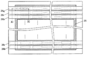
まず、図8,図9に示すように、基板31の表面上に導体膜を成膜し、この導体膜をフォトリソグラフィーによりパターニングし、マトリクス状の画素電極33を形成する。次に、フォトリソグラフィー技術を用いて、画素電極33を囲むように網目状の絶縁膜34を基板31上に形成する。次に、フォトリソグラフィー技術を用いて、絶縁膜34上に画素電極33を1列ずつ囲むように隔壁35を形成する。一方で、有機EL素子の有機化合物層に用いる有機化合物材料を含有させた有機化合物含有液を作成しておく。
First, as shown in FIGS. 8 and 9, a conductor film is formed on the surface of the
そして、有機化合物含有液をノズルから隔壁内の画素電極に向けて噴出させることにより、図10,図11に示すように、隔壁内の画素電極に有機化合物材料36を塗布する。
Then, the organic compound-containing
具体的には、ある隔壁内の画素電極の列の上には、赤色発光用の有機化合物含有液36rが塗布される。その隔壁内の画素電極の列に隣接する一方の列の画素電極の上には、緑色発光用の有機化合物含有液36gが塗布され、他方の列の画素電極の上には、青色発光用の有機化合物含有液36bが塗布される。
Specifically, an organic
このように、赤色発光用、緑色発光用、青色発光用の有機化合物含有液がその順に個別に隔壁内の画素電極上に塗布される。なお、隔壁により、赤、緑、青の各色発光用の有機化合物含有液の混合が防止されている。有機化合物含有液が乾燥することで、有機化合物層が形成される。 Thus, the organic compound containing liquid for red light emission, green light emission, and blue light emission is separately apply | coated on the pixel electrode in a partition in that order. In addition, mixing of the organic compound containing liquid for each color light emission of red, green, and blue is prevented by the partition. The organic compound layer is formed by drying the organic compound-containing liquid.
その後、気相成長法により対向電極を有機化合物層上に形成する。以上により、画素電極と対向電極との間に有機化合物層を挟み込んだ有機EL素子がマトリクス状に配列される。これらの有機EL素子が赤、緑、青の何れかに発光するサブピクセルとなり、画像表示を行うELディスプレイパネルが製造される。
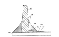
しかし、上述の製造方法では、隔壁の終端部において、図11に示すように、ノズルから噴出される有機化合物含有液36が表面張力により隔壁35に沿って付着するため、乾燥した有機化合物層に膜厚が厚い部分36aができる。一方、有機化合物含有液36が表面張力により隔壁35側に引き寄せられることにより、乾燥させた有機化合物層に膜厚が薄い部分36bができる。このように、有機化合物層の膜厚むらが生じるという問題があった。
However, in the manufacturing method described above, the organic compound-containing
本発明の課題は、上述のような隔壁の側壁における有機化合物層の膜厚むらを抑えた有機化合物層を形成することができるエレクトロルミネッセンスディスプレイパネルの製造方法を提供することである。 An object of the present invention is to provide a manufacturing how the electroluminescent display panel capable of forming an organic compound layer with reduced thickness unevenness of the organic compound layer in the side wall of the partition wall as described above.
以上の課題を解決するため、請求項1に記載の発明は、画素電極、有機EL層、対向電極が積層されてなる表示パネルの製造方法において、
基板に設けられた突出層上に位置する画素配列領域に設けられた複数の前記画素電極を第一の方向において仕切るとともに前記第一の方向に直交する第二の方向に沿って設けられ、前記第二の方向において前記画素配列領域外に開放する複数の隔壁間の複数の前記画素電極にわたって前記第二の方向に沿って連続して有機化合物含有液を塗布し、塗布された前記有機化合物含有液の余分量を前記突出層の側面をつたって前記画素配列領域外に流し落とすことを特徴とする。
In order to solve the above problems, the invention according to claim 1 is a method for manufacturing a display panel in which a pixel electrode, an organic EL layer, and a counter electrode are laminated.
A plurality of the pixel electrodes provided in a pixel array region located on a protruding layer provided on a substrate are partitioned in a first direction and provided along a second direction orthogonal to the first direction; The organic compound-containing liquid is applied by continuously applying the organic compound-containing liquid along the second direction across the plurality of pixel electrodes between the plurality of partition walls that are opened outside the pixel arrangement region in the second direction. An excess amount of the liquid is allowed to flow out of the pixel array region along the side surface of the protruding layer .
請求項1に記載の発明は、前記有機化合物含有液を複数の前記画素電極にわたって連続して塗布することを特徴とする。 The invention described in claim 1 is characterized in that the organic compound-containing liquid is continuously applied over the plurality of pixel electrodes .
請求項1に記載の発明は、前記有機化合物含有液を前記第二の方向に沿って塗布することを特徴とする。 The invention according to claim 1, characterized by applying along said organic compound-containing liquid to the second direction.
請求項2に記載の発明では、前記複数の隔壁は線形状であることを特徴とする。 In the invention described in claim 2, wherein the plurality of partitions is characterized by a linear shape.
請求項1に記載の発明では、前記画素配列領域は基板に設けられた突出層上に位置することを特徴とする。 The invention according to claim 1 is characterized in that the pixel array region is located on a protruding layer provided on a substrate.
請求項3に記載の発明では、前記突出層は、前記側面が傾斜していることを特徴とする。 The invention according to claim 3 is characterized in that the side surface of the protruding layer is inclined.
請求項4に記載の発明は、前記複数の隔壁の末端部に位置し、前記隔壁よりも低く、前記画素電極よりも高い膜を有することを特徴とする。 The invention of claim 4 is located at the distal end of said plurality of partition walls, the lower than the partition wall, and having a high film than the pixel electrode.
本発明によれば、有機化合物層の膜厚のばらつきを抑えることができる。 According to the present invention, variations in the film thickness of the organic compound layer can be suppressed.
以下、本発明を適用した実施の形態について図面を参照して詳細に説明する。ただし、発明の範囲はこれら図示例に限定されるものではない。 Embodiments to which the present invention is applied will be described below in detail with reference to the drawings. However, the scope of the invention is not limited to these illustrated examples.
(第1実施形態)
図1を参照して本実施形態に用いられる塗布装置200について詳細に説明する。塗布装置200は、有機EL素子20のアノードとカソードとの間に積層される有機EL素子層16’を基板11に塗布する装置であり、図1に示すように、x軸ステージ110、ヘッド120、x軸ガイド130、y軸ステージ150、及びコントローラ260等からなる。塗布装置200は、微小の独立した液滴を個々に吐出するインクジェットと異なり、有機化合物溶液を連続して流すノズルコータである。
x軸ステージ110は、コントローラ260から送信される制御信号に応じてx軸ガイド130が案内する方向(x軸方向であり、y軸ステージ150の表面と平行な方向)に移動可能となっている。
(First embodiment)
A
The
x軸ステージ110には、塗布する液体の種類ごとに複数のヘッド120が取り付けられている(図1では1つのみ図示)。ヘッド120には、有機化合物層、例えば、正孔輸送層、赤色発光層、緑色発光層、青色発光層、または、電子輸送層等の各層の材料となる有機化合物材料を溶媒に溶解させた有機化合物溶液、または有機化合物材料を分散媒に分散させた有機化合物分散液が充填されている(以下、有機化合物溶液及び有機化合物分散液を総称して有機化合物含有液とする)。ヘッド120の下端部には、複数のノズルを有する噴射口121が設けられている。各有機化合物含有液は、コントローラ260の指示に応じて各溶液に対応するノズルから所定量ずつ射出される。
A plurality of
y軸ステージ150は、ヘッド120の噴射口121の下方に配置されている。y軸ステージ150は、コントローラ260から送信される制御信号に応じてy軸方向(x軸方向と直交する方向であり、y軸ステージ150の表面と平行な方向)に移動可能となっている。有機化合物材料を塗布する基板11は、y軸ステージ150上に載置される。
The y-
コントローラ260は、x軸ステージ110のx軸方向への移動、y軸ステージ150のy軸方向への移動、及び、噴出口121のノズルからの各溶液の射出を制御する。
The
各有機EL素子20は、図6及び図7に示すように、画素電極13、有機EL層16’及び対向電極17を備えている。画素電極13及び対向電極17は一方がアノード電極として機能し、他方がカソード電極として機能する。これらの有機EL素子20は、縦方向、横方向にそれぞれ規則的に配列されるようにマトリクス状に設けられている。また、図6の縦方向に隣接する有機EL素子20同士は、互いに平行且つ横方向に延在する線形状の複数の隔壁15によって、その有機EL層16’が仕切られている。つまり、有機EL層16’は横方向に沿って複数の有機EL素子20にわたって連続して形成されているが、縦方向には、それぞれ異なる各有機EL層16’が被膜されている。このようにして、横方向に同じ色で発光し、縦方向に互いに異なる色で発光する複数の有機EL層16’が配列されることによって多色発光することができる。
As shown in FIGS. 6 and 7, each
基板11の上には突出層12が設けられ、突出層12内には、図示しないが、画素電極13に各種の信号を出力するために、複数の走査線、信号線等の配線が設けられている。さらに、突出層12内には、各画素電極13に対応して設けられた有機EL素子20を発光するための電流を画素電極13に流す駆動トランジスタ18や、突出層12のコンタクトホール内に充填され、駆動トランジスタ18と画素電極13との間を接続する導電材19や、キャパシタ等の素子(図示せず)が設けられている。これらの素子は、走査線、信号線等の配線の入力信号に応じて画素電極13に電圧を印加する。
A
突出層12の上面は画素配列領域となり、各隔壁15は、画素電極13が配列されている画素配列領域の四辺のうちの対向する二辺に沿って有機EL層16’を仕切っているが、残り対向する二つの辺に沿って有機EL層16’を仕切っていない。つまり、隔壁15は、画素配列領域に設けられた有機EL層16’を図6の平面図の上下方向において仕切るとともに図6の平面図の左右方向において有機EL層16’を画素配列領域外に開放している。
突出層12は、単数又は複数の絶縁膜を備えており、層間絶縁膜、保護絶縁膜、又は平坦化絶縁膜として機能している。
The upper surface of the protruding
The protruding
このような、有機EL素子20の有機EL層16’を成膜する塗布装置200について説明する。図2は基板11の平面図であり、図3は図2のIII−III矢視断面図である。
A
有機EL層16’を形成前の基板11の上面には、複数の走査線、信号線等の配線、複数の駆動トランジスタ18が形成されており、これら配線及び駆動トランジスタ18を被膜するように突出層12が1μm〜15μmの厚さで画素配列領域全域にわたって形成されている。突出層12は、表面が平坦で、側壁がテーパ状に傾斜しており、有機EL素子20が基板11側から光を出射するボトムエミッション型であれば、例えばポリイミドのような透明感光性樹脂膜のような透明な基材が好ましい。突出層12には各駆動トランジスタ18に対応してコンタクトホールが設けられており、コンタクトホール内には導電材19が充填されている。突出層12の上面には、複数の画素電極13が所定の間隔をおいてマトリクス状に配置され、それぞれが各導電材19を介して各駆動トランジスタ18と導通している。
On the upper surface of the
各画素電極13はその周縁を画素電極13よりも高い絶縁膜14に覆われている。換言すれば、絶縁膜14は、各画素電極13の周縁を覆うとともに各画素電極13の中央を露出するような複数の開口部を備えている。
The periphery of each
有機EL層16’となる有機化合物を含有する有機化合物含有液16は、溶媒等に溶解又は分散させた溶液であるため、塗布時の有機化合物含有液16の液面の高さは、有機EL層16’の高さより高くなる。絶縁膜14は、有機EL層16’となる有機化合物含有液16の塗布時の高さより低く、有機化合物含有液16が乾燥して収縮した有機EL層16’より高く設定されている。絶縁膜14は、後述する塗布法によって余剰の有機化合物含有液16が絶縁膜14を乗り越えて自然と画素配列領域外に流れ落ちやすくするように側壁がテーパ状になっている。
そして、縦方向に隣接する画素電極13同士の間の絶縁膜14上には、絶縁膜14より高い隔壁15が設けられている。この隔壁15は、画素電極13と所定の距離だけ離間しており、有機EL素子20の対向電極17に接続される配線として利用することもでき、また絶縁材料で形成してあってもよい。
Since the organic compound-containing
A
画素電極13は、厚さが30nm〜100nmであり、有機EL素子20がボトムエミッション型の場合、例えば錫ドープ酸化インジウム(ITO)、亜鉛ドープ酸化インジウム、酸化インジウム(In2O3)、酸化スズ(SnO2)、酸化亜鉛(ZnO)又はカドミウム−錫酸化物(CTO)のような透明導電膜を突出層12上に成膜し、この透明導電膜をフォトリソグラフィーによりパターニングすることにより形成することができる。また、有機EL素子20がトップエミッション型の場合、アルミニウム等の光反射性金属膜、或いは下層に光反射性金属膜、上層に上述の透明導電膜の積層構造としてもよい。
When the
絶縁膜14は、厚さが150nm〜300nmであり、例えば窒化珪素または酸化珪素等を気相成長法によって成膜し、フォトリソグラフィー法、エッチング法を順次行うことで網目状に形成することができる。対向電極17は、カソード電極である場合、下層となる電子注入層と、電子注入層が酸化されることを防止するとともにシート抵抗を下げる上層となる導電膜との積層構造であり、電子注入層は、仕事関数の低い材料、例えば、マグネシウム、カルシウム、リチウム、バリウム、インジウム、希土類金属の少なくとも一種を含む単体又は合金を有することが好ましく、厚さは0.1nm〜50nmの厚さでよい。
The insulating
導電層は、ボトムエミッション型の場合、光反射性の導電層となり、例えば、アルミニウム、クロム、チタン、ニッケル、タングステン、金、銀、銅の少なくとも一種を含む単体又は合金を有することが好ましく、トップエミッション型の場合、光透過性の導電層となり、例えば、錫ドープ酸化インジウム(ITO)、亜鉛ドープ酸化インジウム、酸化インジウム(In2O3)、酸化スズ(SnO2)、酸化亜鉛(ZnO)又はカドミウム−錫酸化物(CTO)を有することが好ましい。 In the case of the bottom emission type, the conductive layer is a light-reflective conductive layer, and preferably includes, for example, a simple substance or an alloy containing at least one of aluminum, chromium, titanium, nickel, tungsten, gold, silver, and copper. In the case of the emission type, it becomes a light transmissive conductive layer, for example, tin-doped indium oxide (ITO), zinc-doped indium oxide, indium oxide (In 2 O 3 ), tin oxide (SnO 2 ), zinc oxide (ZnO) or It is preferable to have cadmium-tin oxide (CTO).
ここで、複数の有機EL素子20を備えたELディスプレイパネルの製造方法について説明する。
まず、塗布装置200を用いる前に基板11に突出層12、画素電極13、絶縁膜14、隔壁15を形成するので、これらを形成する方法について説明する。
Here, the manufacturing method of EL display panel provided with the some
First, since the protruding
まず、基板11に感光性樹脂膜を成膜し、その感光性樹脂膜を露光・現像することによって、突出層12を形成する。ここで、感光性樹脂がポジ型である場合には、基板11の画素配列領域外を露光し、感光性樹脂がネガ型である場合には、画素配列領域内を露光する。
First, a photosensitive resin film is formed on the
次に、コンタクトホールに導電材19が埋設された突出層12の表面上に導電膜を成膜し、その導電膜に対してフォトリソグラフィー法・エッチング法を施すことによって、画素電極13をマトリクス状に配列するようパターニングする。次に、これら画素電極13をコーティングするよう絶縁膜を成膜し、フォトリソグラフィー法・エッチング法によりその絶縁膜の画素電極13に重なる箇所を除去することによって、絶縁膜14をパターニングする。
Next, a conductive film is formed on the surface of the protruding
次に、絶縁膜14及び画素電極13全体を被覆するよう感光性樹脂膜(例えば、感光性ポリイミド膜)を成膜し、その感光性樹脂膜を露光・現像することによって、画素電極13の各列間に突出層12の左右の縁まで達する複数の隔壁15を互いに独立するよう形成する。
Next, a photosensitive resin film (for example, a photosensitive polyimide film) is formed so as to cover the entire insulating
ここで、感光性樹脂がポジ型である場合には、横方向に並んだ画素電極13の列の上を突出層12の左右の縁まで帯状に露光し、感光性樹脂がネガ型である場合には、横方向に並んだ画素電極13の列と列との間の上を突出層12の左右の縁まで帯状に露光する。
Here, in the case where the photosensitive resin is a positive type, when the photosensitive resin is a negative type, it is exposed in a strip shape up to the left and right edges of the protruding
なお、隔壁が感光性樹脂ではない高分子材料や、金属材料等である場合には、気相成長法、フォトリソグラフィー法、エッチング法を経て隔壁15をパターニングすることができる。
In the case where the partition wall is a polymer material that is not a photosensitive resin, a metal material, or the like, the
以上のようにして、基板11に突出層12、画素電極13、絶縁膜14、隔壁15を形成したら、塗布装置200によって有機化合物層を形成する。
すなわち、まず、基板11の突出層12、画素電極13、絶縁膜14が形成された面を上にして、基板11をy軸ステージ150上に載置する。次いで、コントローラ260によりノズル、x軸ステージ110及びy軸ステージ150を制御し、ノズルを基板11に対して相対的に移動させながら、有機化合物含有液を基板11に塗布し、乾燥させて有機化合物層を形成する。有機EL層16’は、有機化合物からなる発光層を少なくとも一層備えており、この発光層以外に他の有機化合物層或いは無機化合物層を備えていてもよい。
When the protruding
That is, first, the
ここで、画素電極13を陽極とする場合には、有機EL層16’として、例えば正孔輸送層、発光層の順に形成されていてもよいし、発光層の次に電子輸送層が形成されていてもよいし、正孔輸送層が設けられていなくてもよいし、発光層単層であってもよい。
また、画素電極13を陰極とする場合には、有機EL層16’として、例えば電子輸送層、発光層の順に形成されていてもよいし、発光層の次に正孔輸送層が形成されていてもよいし、電子輸送層が設けられていなくてもよい。また、有機EL層16’を形成する前に、画素電極13上に真空蒸着法等により電子注入層を形成してもよい。
Here, when the
When the
図4は塗布装置200により有機化合物含有液16が塗布された基板11の平面図であり、図5は図4のV−V矢視断面図である。有機化合物含有液16は塗布装置200により、隔壁15の長さ方向に塗布されている。有機化合物含有液16は、有機EL層16’となる有機化合物を溶媒等に溶解又は分散させた溶液である。正孔輸送層としては、PEDOT(ポリエチレンジオキシチオフェン)及びPSS(ポリスチレンスルホン酸)の混合物、発光層としては、共役二重結合高分子発光材料が好ましく、溶媒としては、水や、疎水性の有機溶剤(例えば、キシレン、テトラリン、テトラメチルベンゼン、メシチレン)がある。
4 is a plan view of the
2つの隔壁15の間に挟まれる所定の一列の画素電極13及び絶縁膜14上には、塗布装置200のヘッド120とともにx軸方向に移動しながら噴射口121が同一の有機化合物含有液16を塗布し、隔壁15を挟んで隣り合う他の列の画素電極13及び絶縁膜14上には、当該所定の一列の噴射口121と異なる噴射口121が、当該所定の一列の有機EL層16’と異なる色に発光する有機EL層16’となる有機化合物含有液16を塗布する。例えば、ある一列の画素電極13及び絶縁膜14を挟む隔壁15の間には、赤色発光用の有機化合物含有液16rが塗布され、隣接する一方の列の画素電極13及び絶縁膜14を挟む隔壁15の間には、緑色発光用の有機化合物含有液16gが塗布され、隣接する他方の列の画素電極13及び絶縁膜14を挟む隔壁15の間には、青色発光用の有機化合物含有液16bが塗布される。このとき、隔壁15が突出層12の両端まで延在しているため、各色の発光用の有機化合物含有液16r,16g,16bは、隣接する他の発光層用の有機化合物含有液と突出層12上(画素配列領域内)で混合することがない。
On the
塗布装置200の噴射口121は、成膜される有機EL層16’となる有機化合物含有液16の量よりも多い量の有機化合物含有液16を横方向に走査されながら送出する。このとき、図4において、基板11の左右両側には、縦方向に延在する高い隔壁等の仕切りがないため、噴射口121から送出された余剰の有機化合物含有液16が、突出層12の左右両端部に位置する絶縁膜14を乗り越えて絶縁膜14の傾斜された側壁をつたって緩やかに流れ出し、斜面となっている突出層12の側壁から基板11の外周部(画素配列領域外)へ流れ落ちる。
The
このように、隔壁15の両端部において、塗布された有機化合物含有液16の余分量を突出層12から基板11の外周部へ流し落とすことにより、有機化合物含有液16の液面の高さに偏りが小さくなり、有機化合物含有液16の隔壁15との接触面積が小さくなる。このため、隔壁15における表面張力が小さくなり、有機化合物層の膜厚のばらつきを抑えることができる。
In this way, at both ends of the
また、突出層12の外周部では複数色の発光層用の有機化合物含有液16が混合されることになるが、突出層12により画素配列領域と外周部との間に段差が形成されているため、乾燥前の有機化合物含有液16の混合液が段差を乗り越えて画素配列領域に逆流することがない。
In addition, the organic compound-containing
有機化合物含有液16を乾燥させて有機EL層16’を形成したら、有機EL層16’上に対向電極17を形成する。対向電極17は真空蒸着法等により形成することができる。
これにより、画素電極13と対向電極との間に有機EL層16’を挟み込んだ有機EL素子20が基板11上にマトリクス状に形成される。
その後、封止基板(例えば、メタルキャップ、ガラス基板等)を接着剤により対向電極に接着する。これにより、ELディスプレイパネルが完成する。
After the organic compound-containing
Thereby, the
Thereafter, a sealing substrate (for example, a metal cap, a glass substrate, etc.) is bonded to the counter electrode with an adhesive. Thereby, an EL display panel is completed.
以上のように、本実施形態によれば、画素電極13の列が隔壁15により仕切られているので、各列毎に異なる種類の有機化合物含有液16を塗布しても、異なる種類の有機化合物含有液16が画素配列領域で混合することがない。また、余剰の有機化合物含有液16が隔壁15が設けられていない左右両側より絶縁膜14を乗り越えて突出層12の外周部に流出するので、有機EL層の膜厚のばらつきを抑えることができる。
As described above, according to this embodiment, since the columns of the
また、基板11の突出層12が設けられた画素配列領域よりも外に位置する外周部は、突出層12よりも低くなっているので、有機化合物含有液が突出層12の外周部に速やかに流出し、さらに他の有機化合物含有液と混合した混合液が画素配列領域内へ再び流入することを防ぐことができる。
Moreover, since the outer peripheral part located outside the pixel arrangement | positioning area | region in which the
なお、以上の実施形態においては、基板11として、画素電極13に各種の信号を出力する複数の走査線、信号線等の配線、及び、各画素電極13に対応した駆動トランジスタ18やキャパシタ等の素子(図示せず)が設けられたトランジスタアレイパネルを用いたが、本発明はこれに限らず、例えばパッシブ駆動のパネルを用いてもよい。
In the above embodiment, the
11 基板
12 突出層
13 画素電極(画素電極)
15 隔壁
16 有機化合物含有液
11
15
Claims (4)
基板に設けられた突出層上に位置する画素配列領域に設けられた複数の前記画素電極を第一の方向において仕切るとともに前記第一の方向に直交する第二の方向に沿って設けられ、前記第二の方向において前記画素配列領域外に開放する複数の隔壁間の複数の前記画素電極にわたって前記第二の方向に沿って連続して有機化合物含有液を塗布し、塗布された前記有機化合物含有液の余分量を前記突出層の側面をつたって前記画素配列領域外に流し落とすことを特徴とする表示パネルの製造方法。 In a method for manufacturing a display panel in which a pixel electrode, an organic EL layer, and a counter electrode are laminated,
A plurality of the pixel electrodes provided in a pixel array region located on a protruding layer provided on a substrate are partitioned in a first direction and provided along a second direction orthogonal to the first direction; The organic compound-containing liquid is applied by continuously applying the organic compound-containing liquid along the second direction across the plurality of pixel electrodes between the plurality of partition walls that are opened outside the pixel arrangement region in the second direction. A method for manufacturing a display panel, characterized in that an excess amount of liquid is allowed to flow out of the pixel array region along a side surface of the protruding layer .
Priority Applications (1)
| Application Number | Priority Date | Filing Date | Title |
|---|---|---|---|
| JP2005272182A JP4687351B2 (en) | 2005-09-20 | 2005-09-20 | Manufacturing method of display panel |
Applications Claiming Priority (1)
| Application Number | Priority Date | Filing Date | Title |
|---|---|---|---|
| JP2005272182A JP4687351B2 (en) | 2005-09-20 | 2005-09-20 | Manufacturing method of display panel |
Publications (3)
| Publication Number | Publication Date |
|---|---|
| JP2007087640A JP2007087640A (en) | 2007-04-05 |
| JP2007087640A5 JP2007087640A5 (en) | 2008-11-06 |
| JP4687351B2 true JP4687351B2 (en) | 2011-05-25 |
Family
ID=37974424
Family Applications (1)
| Application Number | Title | Priority Date | Filing Date |
|---|---|---|---|
| JP2005272182A Expired - Fee Related JP4687351B2 (en) | 2005-09-20 | 2005-09-20 | Manufacturing method of display panel |
Country Status (1)
| Country | Link |
|---|---|
| JP (1) | JP4687351B2 (en) |
Families Citing this family (2)
| Publication number | Priority date | Publication date | Assignee | Title |
|---|---|---|---|---|
| JP5061562B2 (en) * | 2006-09-29 | 2012-10-31 | セイコーエプソン株式会社 | LIGHT EMITTING DEVICE AND ELECTRONIC DEVICE |
| JP5168121B2 (en) * | 2008-12-12 | 2013-03-21 | カシオ計算機株式会社 | LIGHT EMITTING PANEL AND METHOD FOR MANUFACTURING LIGHT EMITTING PANEL |
Citations (4)
| Publication number | Priority date | Publication date | Assignee | Title |
|---|---|---|---|---|
| JP2001189192A (en) * | 1999-10-12 | 2001-07-10 | Semiconductor Energy Lab Co Ltd | Light emission device and manufacturing method of the same |
| JP2004288403A (en) * | 2003-03-19 | 2004-10-14 | Optrex Corp | Manufacturing method of organic el display and organic el display |
| JP2005078946A (en) * | 2003-08-29 | 2005-03-24 | Semiconductor Energy Lab Co Ltd | Electronic apparatus, semiconductor device, and its manufacturing method |
| JP2005100979A (en) * | 2003-08-29 | 2005-04-14 | Semiconductor Energy Lab Co Ltd | Display device and its method of manufacture |
-
2005
- 2005-09-20 JP JP2005272182A patent/JP4687351B2/en not_active Expired - Fee Related
Patent Citations (4)
| Publication number | Priority date | Publication date | Assignee | Title |
|---|---|---|---|---|
| JP2001189192A (en) * | 1999-10-12 | 2001-07-10 | Semiconductor Energy Lab Co Ltd | Light emission device and manufacturing method of the same |
| JP2004288403A (en) * | 2003-03-19 | 2004-10-14 | Optrex Corp | Manufacturing method of organic el display and organic el display |
| JP2005078946A (en) * | 2003-08-29 | 2005-03-24 | Semiconductor Energy Lab Co Ltd | Electronic apparatus, semiconductor device, and its manufacturing method |
| JP2005100979A (en) * | 2003-08-29 | 2005-04-14 | Semiconductor Energy Lab Co Ltd | Display device and its method of manufacture |
Also Published As
| Publication number | Publication date |
|---|---|
| JP2007087640A (en) | 2007-04-05 |
Similar Documents
| Publication | Publication Date | Title |
|---|---|---|
| JP5061562B2 (en) | LIGHT EMITTING DEVICE AND ELECTRONIC DEVICE | |
| JP4318455B2 (en) | Color filter forming method, light emitting element layer forming method, color display device manufacturing method using the same, or color display device | |
| JP4924314B2 (en) | Organic EL device and electronic device | |
| JP3951445B2 (en) | Organic EL element, display device, optical device, organic EL element manufacturing method, display device manufacturing method, and optical device manufacturing method | |
| US7724323B2 (en) | Pattern-forming method for manufacturing device having partitioning layer formed on foundation layer with preliminary partitioning and residue fragment formed by removing part of partitioning layer | |
| US9773848B2 (en) | Organic EL display panel, production method therefor, and organic EL display device | |
| JP2007115529A (en) | Display device and its manufacturing method | |
| JP5168121B2 (en) | LIGHT EMITTING PANEL AND METHOD FOR MANUFACTURING LIGHT EMITTING PANEL | |
| JP4226867B2 (en) | Display device | |
| US7784425B2 (en) | Droplet ejecting apparatus, electro-optic device, electronic apparatus, and droplet ejecting method | |
| US11158681B2 (en) | OLED display device and method of manufacturing OLED display device | |
| JP2007280866A (en) | Thin membrane device, organic el device and liquid crystal display device, electronic unit, manufacturing method of thin membrane device, manufacturing method of organic el device and manufacturing method of liquid crystal display device | |
| JP4019791B2 (en) | Deposition equipment | |
| US8580335B2 (en) | Method for discharging liquid body, method for manufacturing color filter, and method for manufacturing organic EL device | |
| US20060152559A1 (en) | Pattern formation method, method for manufacturing color filter, color filter, method for manufacturing electro-optical device, and electro-optical device | |
| JP4687351B2 (en) | Manufacturing method of display panel | |
| KR20160067544A (en) | Organic light emitting diode display device and method of manufacturing the same | |
| JP4957477B2 (en) | Manufacturing method of organic EL device | |
| JP2008066054A (en) | Electro-optical device and its manufacturing method | |
| JP4506788B2 (en) | EL panel manufacturing method | |
| JP2011014358A (en) | Method and device for manufacturing light-emitting panel | |
| JP2011096375A (en) | Optical device, method of manufacturing the same, and electronic apparatus | |
| JP6337088B2 (en) | Organic EL display panel and organic EL display device | |
| JP2006163432A (en) | Color filter, display device, optical apparatus, manufacturing method of color filter, manufacturing method of display device and manufacturing method of optical apparatus | |
| JP2021012811A (en) | Manufacturing method of self-luminous display panel and functional layer forming device |
Legal Events
| Date | Code | Title | Description |
|---|---|---|---|
| A521 | Request for written amendment filed |
Free format text: JAPANESE INTERMEDIATE CODE: A523 Effective date: 20080917 |
|
| A621 | Written request for application examination |
Free format text: JAPANESE INTERMEDIATE CODE: A621 Effective date: 20080917 |
|
| A977 | Report on retrieval |
Free format text: JAPANESE INTERMEDIATE CODE: A971007 Effective date: 20100917 |
|
| A131 | Notification of reasons for refusal |
Free format text: JAPANESE INTERMEDIATE CODE: A131 Effective date: 20101012 |
|
| A521 | Request for written amendment filed |
Free format text: JAPANESE INTERMEDIATE CODE: A523 Effective date: 20101210 |
|
| RD02 | Notification of acceptance of power of attorney |
Free format text: JAPANESE INTERMEDIATE CODE: A7422 Effective date: 20101210 |
|
| TRDD | Decision of grant or rejection written | ||
| A01 | Written decision to grant a patent or to grant a registration (utility model) |
Free format text: JAPANESE INTERMEDIATE CODE: A01 Effective date: 20110118 |
|
| A01 | Written decision to grant a patent or to grant a registration (utility model) |
Free format text: JAPANESE INTERMEDIATE CODE: A01 |
|
| A61 | First payment of annual fees (during grant procedure) |
Free format text: JAPANESE INTERMEDIATE CODE: A61 Effective date: 20110131 |
|
| R150 | Certificate of patent or registration of utility model |
Ref document number: 4687351 Country of ref document: JP Free format text: JAPANESE INTERMEDIATE CODE: R150 Free format text: JAPANESE INTERMEDIATE CODE: R150 |
|
| FPAY | Renewal fee payment (event date is renewal date of database) |
Free format text: PAYMENT UNTIL: 20140225 Year of fee payment: 3 |
|
| R250 | Receipt of annual fees |
Free format text: JAPANESE INTERMEDIATE CODE: R250 |
|
| S111 | Request for change of ownership or part of ownership |
Free format text: JAPANESE INTERMEDIATE CODE: R313113 |
|
| R350 | Written notification of registration of transfer |
Free format text: JAPANESE INTERMEDIATE CODE: R350 |
|
| R250 | Receipt of annual fees |
Free format text: JAPANESE INTERMEDIATE CODE: R250 |
|
| R250 | Receipt of annual fees |
Free format text: JAPANESE INTERMEDIATE CODE: R250 |
|
| LAPS | Cancellation because of no payment of annual fees |