JP4679735B2 - Field discrimination method, field discrimination circuit, and field discrimination device - Google Patents
Field discrimination method, field discrimination circuit, and field discrimination device Download PDFInfo
- Publication number
- JP4679735B2 JP4679735B2 JP2001045973A JP2001045973A JP4679735B2 JP 4679735 B2 JP4679735 B2 JP 4679735B2 JP 2001045973 A JP2001045973 A JP 2001045973A JP 2001045973 A JP2001045973 A JP 2001045973A JP 4679735 B2 JP4679735 B2 JP 4679735B2
- Authority
- JP
- Japan
- Prior art keywords
- signal
- pulse signal
- synchronization signal
- signal indicating
- indicating
- Prior art date
- Legal status (The legal status is an assumption and is not a legal conclusion. Google has not performed a legal analysis and makes no representation as to the accuracy of the status listed.)
- Expired - Fee Related
Links
Images


Description
【0001】
【発明の所属する技術分野】
本発明は、映像信号をディジタル信号として扱う信号処理システムにおいて、特に、インタレースした映像信号の垂直同期信号と水平同期信号の位相関係から、奇数フィールドか偶数フィールドかのフィールド判別を行うフィールド判別方法、及びフィールド判別装置に関するものである。
【0002】
【従来の技術】
映像信号をディジタル信号として扱う信号処理システムにおいて、垂直同期信号と水平同期信号の位相関係からフィールド判別を行う方法としては、垂直同期信号が発生した後、1/2 水平同期期間内に水平同期信号が発生するかどうかを判断することによってフィールド判別する方法が知られている。
【0003】
以下に、この従来の技術によるフィールド判別方法を図6を用いて説明する。なお、以下の説明では取り扱う映像信号の1フレームあたりの水平走査線数が525本のインタレース信号であるものを例にとって説明する。
一般に、フィールド判別方法には、垂直同期信号と水平同期信号が用いられ、垂直同期信号と水平同期信号は、ディジタル信号処理系の信号として扱われ、垂直同期信号と水平同期信号は、各々ディジタル信号処理系の1クロック幅のパルス信号に整形される。
【0004】
図6において、vpls、hplsは、垂直同期信号と水平同期信号を各々のディジタル信号処理系の1クロック幅の信号に整形したものであり、vplsは、垂直同期信号に対して得られる1クロック幅のパルス信号を示し、hplsは水平同期信号に対して得られる1クロック幅のパルス信号を示す。また、hhlfは、前記vplsに基づいて生成され、入力された映像信号の1/2 水平同期期間を特定する信号である。fidは、奇数フィールドか偶数フィールドかの判別結果を示すフィールド判定別信号である。
【0005】
以下、このフィールド判別信号fidを生成する方法について説明する。
まず、入力された垂直同期信号に対して得られるvplsがアクティブとなった時点401で、フィールド判別信号fidをLに初期化し、hhlfを、扱っている映像信号の1水平同期期間の半分の期間アクティブにする。このhhlfがアクティブとなっている期間中に、入力された水平同期信号に対して得られるhplsがアクティブとなる場合、例えば図6に示すnの場合には、フィールド判別信号fidを反転させ、fidをHに変化させる。
【0006】
また、次にvpls がアクティブとなった時点402でフィールド判別信号fidをLに初期化し、扱っている映像信号の1水平同期期間の半分の期間hhlfをアクティブにする。なお、この402の時点でhhlfがアクティブとなっている期間は、図6に示すように、垂直同期信号と水平同期信号の位相関係から hpls がアクティブとなることはない。そのため、この位相関係よりフィールド判別信号fidは次のvpls403までLを保ったままとなる。
以上のような動作を繰り返すことにより、垂直同期信号と水平同期信号の位相関係からフィールド判別信号 fid を生成することができる。
【0007】
【発明が解決しようとする課題】
しかしながら、前述したようなフィールド判別方法では、フィールド判別信号fidを生成する際に、hhlfとして、扱っている映像信号の1/2 水平同期期間を特定する必要があり、例えば 13.5MHz で動作している信号処理システムでは、429までカウントし得る9ビットカウンタが必要となる。
【0008】
また、入力される映像信号によって1フレームあたり525水平走査線からなる映像信号と、1フレームあたり1125水平走査線からなる映像信号とを切替えて使用するシステムの場合には、入力される映像信号の1/2水平同期期間が各々異なるため、映像信号毎に 1/2 水平同期期間がそのシステムクロックの何クロックに相当するかを設定変更する必要がある。
なお、設定変更は CPU などからのレジスタ設定による方法が一般的であるが、この場合どちらの映像信号を扱っているかを CPU が知る必要がある。
【0009】
本発明は、このような従来の課題を鑑みてなされたものであり、扱っている映像信号の1/2水平同期期間を特定することなく、一意にフィールド判別信号を生成することができるフィールド判別方法、及び回路を提供することを目的とする。
【0010】
【課題を解決するための手段】
前記課題を解決するために、本発明にかかるフィールド判別方法は、インタレースした映像信号の垂直同期信号を示すパルス信号と水平同期信号を示すパルス信号とから生成した状態信号に基づいて、フィールド判別信号を生成するフィールド判別方法であって、前記垂直同期信号を示すパルス信号と前記水平同期信号を示すパルス信号が同じタイミングでアクティブとなる時には、当該垂直同期信号を示すパルス信号と前記水平同期信号を示すパルス信号とが同時にアクティブとなる毎に前記状態信号の論理値をHとし、前記垂直同期信号を示すパルス信号と前記水平同期信号を示すパルス信号とが異なるタイミングでアクティブとなる時には、前記垂直同期信号を示すパルス信号がアクティブとなる毎に前記状態信号の論理値をLにするとともに、前記水平同期信号を示すパルス信号がアクティブとなる毎に前記状態信号の論理値を以前の論理値から反転させ、前記垂直同期信号を示すパルス信号がアクティブとなった時点での前記状態信号の論理値をフィールド判別信号とすることを特徴とするものである。
【0011】
また、本発明にかかるフィールド判別方法は、インタレースした映像信号の垂直同期信号を示すパルス信号と水平同期信号を示すパルス信号とから生成した状態信号に基づいて、フィールド判別信号を生成するフィールド判別方法であって、前記垂直同期信号を示すパルス信号と前記水平同期信号を示すパルス信号が同じタイミングでアクティブとなる時には、当該垂直同期信号を示すパルス信号と前記水平同期信号を示すパルス信号とが同時にアクティブとなる毎に前記状態信号の論理値をLとし、前記垂直同期信号を示すパルス信号と前記水平同期信号を示すパルス信号とが異なるタイミングでアクティブとなる時には、前記垂直同期信号を示すパルス信号がアクティブとなる毎に前記状態信号の論理値をHにするとともに、前記水平同期信号を示すパルス信号がアクティブとなる毎に前記状態信号の論理値を以前の論理値から反転させ、前記垂直同期信号を示すパルス信号がアクティブとなった時点での前記状態信号の論理値をフィールド判別信号とすることを特徴とするものである。
【0012】
また、本発明にかかるフィールド判別方法は、前記垂直同期信号を示すパルス信号と前記水平同期信号を示すパルス信号は、それぞれ1クロック幅のパルス信号であることを特徴とするものである。
【0013】
また、本発明にかかるフィールド判別回路は、インタレースした映像信号の垂直同期信号を示すパルス信号と水平同期信号を示すパルス信号とに基づいて、フィールド判別信号を生成するフィールド判別回路であって、前記垂直同期信号を示すパルス信号と前記水平同期信号を示すパルス信号の論理ORを取った信号がトリガとして入力されるまで現在の論理値を保持し、前記垂直同期信号を示すパルス信号と前記水平同期信号を示すパルス信号が同じタイミングでトリガとなる時には、当該垂直同期信号を示すパルス信号と前記水平同期信号を示すパルス信号とが同時にトリガとして入力される毎に論理値をHとし、前記垂直同期信号を示すパルス信号と前記水平同期信号を示すパルス信号が異なるタイミングでトリガとなる時には、前記垂直同期信号を示すパルス信号がトリガとして入力される毎に論理値をLにするとともに、前記水平同期信号を示すパルス信号がトリガとして入力される毎に論理値を以前の論理値から反転させる第1の論理回路と、前記垂直同期信号を示すパルス信号がトリガとして入力されるまで現在の論理値を保持し、前記垂直同期信号を示すパルス信号がトリガとして入力された時点で前記第1の論理回路が保持している論理値をフィールド判別信号として出力する第2の論理回路とを有することを特徴とするものである。
【0014】
また、本発明にかかるフィールド判別回路は、インタレースした映像信号の垂直同期信号を示すパルス信号と水平同期信号を示すパルス信号とに基づいて、フィールド判別信号を生成するフィールド判別回路であって、前記垂直同期信号を示すパルス信号と前記水平同期信号を示すパルス信号の論理ORを取った信号がトリガとして入力されるまで現在の論理値を保持し、前記垂直同期信号を示すパルス信号と前記水平同期信号を示すパルス信号が同じタイミングでトリガとなる時には、当該垂直同期信号を示すパルス信号と前記水平同期信号を示すパルス信号とが同時にトリガとして入力される毎に論理値をLとし、前記垂直同期信号を示すパルス信号と前記水平同期信号を示すパルス信号が異なるタイミングでトリガとなる時には、前記垂直同期信号を示すパルス信号がトリガとして入力される毎に論理値をHにするとともに、前記水平同期信号を示すパルス信号がトリガとして入力される毎に論理値を以前の論理値から反転させる第1の論理回路と、前記垂直同期信号を示すパルス信号がトリガとして入力されるまで現在の論理値を保持し、前記垂直同期信号を示すパルス信号がトリガとして入力された時点で前記第1の論理回路が保持している論理値をフィールド判別信号として出力する第2の論理回路とを有することを特徴とするものである。
【0015】
また、本発明にかかるフィールド判別回路は、前記垂直同期信号を示すパルス信号と前記水平同期信号を示すパルス信号は、それぞれ1クロック幅のパルス信号であることを特徴とするものである。
【0016】
また、本発明にかかるフィールド判別装置は、前記本発明にかかるフィールド判別回路と、前記フィールド判別回路から出力されたフィールド判別信号を入力として当該フィールド判定信号の論理値を反転させる反転設定回路と、前記反転設定回路を制御する反転設定制御回路とからなることを特徴とするものである。
【0017】
【発明の実施の形態】
本発明にかかるフィールド判別方法は、インターレースした映像信号の垂直同期信号と水平同期信号から、フィールド判別を初期状態によらず一意に決定することができるものである。
【0018】
(実施の形態1)
以下、本発明の実施の形態1によるフィールド判別方法について図1から図5を用いて説明する。なお、以下の説明では取り扱う映像信号が、1フレームあたりの水平走査線数が525本のインタレース信号であるものを例にとって説明する。
【0019】
フィールド判別方法には、垂直同期信号と水平同期信号が用いられる。垂直同期信号と水平同期信号は、ディジタル信号処理系の信号として扱われ、垂直同期信号と水平同期信号は、各々ディジタル信号処理系の1クロック幅の信号に整形される。なお、1クロック幅のパルス信号は、例えば、垂直同期信号と水平同期信号の立上りエッジを検出することによって垂直同期信号と水平同期信号それぞれに対する1クロック幅のパルス信号が得られる。
【0020】
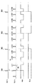
図1は、本発明の実施の形態1によるフィールド判別方法を説明するためのタイミング図の一例であり、垂直同期信号を示すパルス信号と水平同期信号を示すパルス信号とが常に異なるタイミングでアクティブとなる場合を示すものである。
【0021】
図1において、vplsは、垂直同期信号に対して得られる1クロック幅のパルス信号を示し、101、102、103、104は、vplsの論理が正となるタイミングを示す。また、hplsは水平同期信号に対して得られる1クロック幅のパルス信号を示し、n、n+1、…、n+788は、hplsの論理が正となるタイミングを示す。
【0022】
heoは、vplsとhplsとから生成される状態信号であり、vpls が生成される時点では、heo の論理値を常にLに変化させ、また、hpls が生成される毎に、heo の論理値を反転させる。また、fidは、vplsとheoから生成されるフィールド判定別信号であり、vpls が生成された時点での heo の論理値を示すものである。
【0023】
以下、状態信号であるheoの生成動作について説明する。
図1に示すように、heoの初期値は不定であり、最初のvpls101が生成された時点でheoをLに初期化され、次のhpls nが生成された時点で、heoをLからHへと変化させる。以降、hplsが生成されるたびにheoを反転する。
【0024】
なお、図1は、vpls101が生成されてから最初のhplsが生成されるまでの期間が入力された映像信号の1/2水平同期期間内となるものであり、インターレース信号の垂直同期信号と水平同期信号の位相関係からこのような場合には、最初のvpls101が生成されてから次のvpls102が生成されるまでの期間に生成されるhpls数は、常に奇数回数となる。
よって、vpls101でLに初期化されたheoは、奇数回反転し、次のvpls102が生成される時点でheoは、常にHとなる。
【0025】
同様に、インターレース信号の垂直同期信号と水平同期信号の位相関係からvpls102から次のvpls103までの期間に生成されるhpls数は、偶数回数となる。よって、vpls101でLであったheoは、偶数回反転し、次のvplsが生成される時点でheoは、常にLとなる。
【0026】
なお、vpls103が生成された時点では、heoが既にLとなっているので論理値をLに変化させるという動作によって論理値が変化することはない。
【0027】
このような動作により、vplsが生成された時点でのheoは、直前のvplsと現vplsとの間のhpls数が奇数の場合には、常にHとなり、偶数の場合には、常にLとなる。
【0028】
次に、fidの生成動作について説明する。
fidの初期値は不定であり、vplsが生成された時点で、その時点におけるheoの論理値をフィールド判別信号fidとして出力する。ただし、最初のvpls101が生成された時点では heoの論理値は不定であるため、fid は不定のままである。
【0029】
vpls 102が生成された時点では、heoはHであるのでこの時点で fid は H として確定する。また、次のvpls 103が生成された時点では、heoは Lであり、この時点でfidはLに変化する。以降、同様の動作を繰り返すことによりfidは、各フィールド毎に常にHあるいはLとして確定する。
【0030】
このように、インタレースした映像信号の垂直同期信号と水平同期信号の位相関係からフィールド判別信号fidは、一意に決まり、フィールド判別信号fidの初期状態によりその極性が変わるということはない。また、フィールド判別信号fidの論理値H、Lに対して、どちらが奇数フィールドでどちらが偶数フィールドであるかについては、入力している映像信号によってあらかじめ決まっているので、フィールド判別信号fidを使用して各フィールド毎に処理内容を変えるシステムであっても初期状態によらず各フィールドに対して適切な処理を行うことができることになる。
【0031】
次に、図2は、本発明の実施の形態1によるフィールド判別方法を説明するためのタイミング図の一例であり、垂直同期信号を示すパルス信号と水平同期信号を示すパルス信号とが常に異なるタイミングでアクティブとなる場合を示すものである。
【0032】
図2は、最初のvpls201が生成されてから最初のhplsが生成されるまでの期間が入力された映像信号の1/2水平同期期間以上となっているが、heo、fidの再生動作は、図1を用いて説明したフィールド判別方法と全く同様であり、図1を用いて説明したフィールド判別方法と同様に、インタレースした映像信号の垂直同期信号と水平同期信号の位相関係に基づいて、初期状態によらず一意にフィールド判別信号を生成することができる。
【0033】
なお、上記図1、図2を用いて説明したフィールド判別方法では、vplsが生成される時点でheoの理論値をLに変化させたが、vplsが生成される時点でheoの理論理をHに変化させてもよい。なお、この場合には、vplsが生成された時点でのheoは、直前のvplsと現vplsとの間のhplsが奇数の場合にはLとなり、偶数の場合にはHとなって、fidの極性も前述したフィールド判別方法で求めた結果と逆になる。
【0034】
次に、vplsとhplsが同時に生成される場合について説明する。
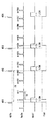
図3は、本発明の実施の形態1によるフィールド判別方法を説明するためのタイムング図の一例であり、垂直同期信号を示すパルス信号と水平同期信号を示すパルス信号とが同じタイミングでアクティブとなる場合を含んでいるものである。
【0035】
図3のvpls301やvpls303で示すタイミングのように、 vpls と hpls が同時に生成された場合には、例外的にheoを H に変化させる。一方、vpls302やvpls304で示すタイミングのように、vplsのみが生成されている場合には、図1、図2で示した場合と同様に heo を L に変化させる。なお、その他の動作は、図1、図2を用いて説明した前記フィールド判別方法の場合と同様である。
【0036】
このように vpls と hpls が同時に生成されるような位相関係にある場合でも、インタレースした映像信号の垂直同期信号と水平同期信号の位相関係に基づいて、初期状態によらず一意にフィールド判別信号を生成することが可能となる。
【0037】
なお、上記の図3を用いた説明では、vpls と hpls が同時に生成される時点でのheoの論理値をHとし、vplsのみが生成されるタイミングでのheoの論理値をLとするものについて説明したが、vplsとhplsが同時に生成される時点での heoの論理値をLとし、vplsのみが生成されるタイミングでのheoの論理値をHとするものであってもよい。なお、vplsとhplsが同時に生成される時点でのheoの論理値をLとし、vplsのみが生成されるタイミングでのheoの論理値をHとした場合には、fidの極性は上記の説明とは逆となる。
【0038】
(実施の形態2)
以下に、前記実施の形態1において説明したフィールド判別方法を実現する,フィールド判定回路の一例について図4を用いて説明する。
図4は、本発明の実施の形態2によるフィールド判別回路を説明するための回路図である。
【0039】
図4において、本発明の実施の形態2によるフィールド判別回路は、AND回路とOR回路とからなる論理ブロック201、202、203と、Dタイプのフリップフロップ204、205と、OR回路206とからなる。
【0040】
論理ブロック201、202は、フリップフロップ204、205のイネーブル動作を実現するものであり、論理ブロック201は、OR回路206と組み合わせることにより、vpls と hpls が同時に H になった場合にのみ端子207の論理値をフリップフロップ204にラッチさせるものである。また、論理ブロック202は、vplsがHになった場合にのみ端子208の論理値をフリップフロップ205にラッチさせるものである。
【0041】
すなわち、フリップフロップ204の出力heoは、vplsあるいはhplsがHとなるまでそれ以前の値を保持し続け、vplsあるいはhplsがHとなった時点で、端子207の論理値に更新されるものであり、また フリップフロップ205の出力fidは、vplsがHとなるまで値を保持し続け、vplsがHとなった時点で、そのときの端子208の論理値に更新されるものである。
【0042】
論理ブロック203は、heoを反転しvplsが発生した際にフリップフロップ204の出力heoをLとする論理210と、vplsとhpslが同時に発生した場合に、端子209の論理値をHとする論理211と、論理210と論理211の論理値のORを取る論理212から成る。
【0043】
この論理ブロック203と、論理ブロック201と論理206と、フリップフロップ204の組み合わせにより、heoをhplsが発生する毎に反転し、vplsが発生した際には、heoをLとし、vplsとhpslが同時に発生した場合には、heoをHとする第1の論理回路を実現している。
【0044】
また、論理ブロック202とフリップフロップ205の組み合わせにより、vplsが発生した時点でのheoの論理値をfidとする第2の論理回路を実現している。
【0045】
このように構成された前記第1の論理回路と前記第2の論理回路を組み合せることにより、フリップフロップ2個と簡単な論理回路から成る小規模な回路を用いて、インタレースした映像信号の垂直同期信号と水平同期信号の位相関係から初期状態によらず一意にフィールド判別信号を生成することが可能となる。
【0046】
また、上記で説明した論理値を反転させて同様の動作を実現することも可能であり、例えば、論理ブロック203の論理210が、heoを反転し、vplsが発生した際にheoをHとする論理に置き換えるとともに、論理211が、vplsとhpslが同時に発生した場合には、端子 209 をLとする論理に置き換えるようにしても同様の動作が得られる。なお、この場合には、fidの極性は上記の説明とは反転した論理値となる。
【0047】
(実施の形態3)
次に、前記実施の形態1で説明したフィールド判別方法により得られたフィールド判別信号を用いて、映像信号に対して処理を行うフィールド判別装置について説明する。
【0048】
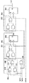
図5は、本発明の実施の形態3にかかるフィールド判別装置を説明するためのブロック図である。
図5において、フィールド判別装置は、パルス信号生成回路501と、フィールド判別回路502と、反転設定制御回路503と、反転設定回路504と、映像信号処理回路505と、映像信号表示回路506とからなる。
【0049】
パルス信号生成回路501は、垂直同期信号と水平同期信号をそれぞれ入力とし、垂直同期信号を示す1クロック幅のパルス信号であるvplsと、水平同期信号を示す1クロック幅のパルス信号であるhplsを生成し、フィールド判別回路502に出力する。
【0050】
また、フィールド判別回路502では、前記実施の形態1により示したフィールド判別方法により、フィールド判定信号fidを生成し、生成したフィールド判別信号 fid を反転設定回路504に出力する。
【0051】
反転設定制御回路503は、フィールド判別信号fidの論理値H、Lに対して、どちらが奇数フィールドでどちらが偶数フィールドであるかについて決定し、反転設定回路504を制御する。
【0052】
反転設定回路504は、反転設定制御回路503の制御に基づいて、フィールド判別信号の論理値と映像信号のフィールドとが一致するように、フィールド判別信号 fid の論理値を必要に応じて反転させ、映像信号処理回路505に出力する。
【0053】
映像信号処理回路505は、反転設定回路504から出力されたフィールド判別信号に基づいて、映像信号に対して奇数フィールドと偶数フィールドの各々に対して適切な処理を行い、映像信号表示回路506に出力する。
映像信号表示回路506は、映像信号処理回路505により処理された映像信号を表示する。
【0054】
次に、本発明の実施の形態3によるフィールド判定装置の動作について説明する。
パルス信号生成回路501は、入力された垂直同期信号と水平同期信号から垂直同期信号を示す1クロック幅のパルス信号であるvplsと、水平同期信号を示す1クロック幅のパルス信号であるhplsを生成する。フィールド判別回路502は、パルス信号生成回路501により生成されたvpls、及びhplsからフィールド判定信号fidを生成し、生成したフィールド判別信号 fid を反転設定回路504に出力する。なお、フィールド判別回路502によるフィールド判別方法は、前記実施の形態1で説明したものと同様であるためここでは説明を省略する。
【0055】
反転設定制御回路503は、映像処理を行なうシステムに応じて、奇数フィールドと偶数フィールドの相対的な関係を適切に保つように、反転設定回路504を制御し、フィールド判定回路502から出力されたフィールド判別信号fidを必要に応じて反転させる。
【0056】
これは、フィールド判別回路502で生成されたフィールド判別信号 fidの論理値が、映像信号の奇数フィールド、偶数フィールドのどちらを示すものとなるかが、システムによって異なるためであり、フィールド毎に処理内容を変えるシステムにおいては、フィールド判別信号fidの論理値と、映像信号のフィールドの関係を適切に保つ必要があるためである。
【0057】
また、例えば、フレームあたり525本の水平走査線からなるインタレースした映像信号に対する処理と、フレームあたり1125本の水平走査線からなるインタレースした映像信号に対する処理とを切替えて行うシステムにおいては、それぞれの映像信号に対するフィールド判別信号 fid の論理値と、映像信号の奇数フィールド、偶数フィールドとがそれぞれ異なる場合もあるが、反転設定制御回路503により、常にフィールド判別信号の論理値と、映像信号の奇数フィールド、偶数フィールドとの相対的な関係を適切に保つことにより、それぞれのフィールドの映像信号に対する適切な処理を行うことができる。
【0058】
次に、反転設定回路504により奇数フィールドと偶数フィールドの相対的な関係を適切に保つように反転設定されたフィールド判別信号は、映像信号処理回路505に入力される。映像信号処理回路505は、入力されたフィールド判別信号に基づいて映像信号に対して奇数フィールドと偶数フィールドの各々に対して適切な処理を行い、映像信号表示回路506に出力する。
映像信号表示回路506は、映像信号処理回路により処理が行われた映像信号を表示する。
【0059】
これにより、垂直同期信号と水平同期信号の位相関係からフィールド判別信号を初期状態によらず一意に生成することができるとともに、フィールド判別信号の論理値と、映像信号の奇数フィールドと偶数フィールドの相対的な関係を適切に保つことができ、映像信号処理回路505によりそれぞれのフィールドの映像信号に対する適切な処理を行うことができる。
【0060】
【発明の効果】
本発明にかかるフィールド判別方法は、入力される垂直同期信号と水平同期信号の位相関係から1/2水平同期期間を特定することなく、フィールド判別を行うことにより、初期状態によらず一意にフィールド判別を行うことができる。
【0061】
また、本発明にかかるフィールド判別回路は、フリップフロップ2個と簡単な論理回路から成る小規模な回路により、初期状態によらずフィールド判別信号を一意に生成することができる。
【0062】
また、本発明にかかるフィールド判別装置は、垂直同期信号と水平同期信号の位相関係からフィールド判別信号を初期状態によらず一意に生成することができるとともに、フィールド判別信号の論理値と、映像信号の奇数フィールドと偶数フィールドの相対的な関係を適切に保つことができ、映像信号処理回路により適切な映像信号の処理を行うことができる。
【図面の簡単な説明】
【図1】本発明の実施の形態1によるフィールド判別方法の一例を説明するためのタイミング図
【図2】本発明の実施の形態1によるフィールド判別方法の一例を説明するためのタイミング図
【図3】本発明の実施の形態1によるフィールド判別方法の一例を説明するためのタイミング図
【図4】本発明の実施の形態2によるフィールド判別回路の一例を説明するための回路図
【図5】本発明の実施の形態3によるフィールド判別装置の一例を説明するためのブロック図
【図6】本発明に対する従来例のフィールド判別回路の一例を説明するためのタイミング図
【符号の説明】
201、202、203 論理ブロック
204、205 フリップフロップ
206、210、212 OR回路
211 AND回路
501 パルス信号生成回路
502 フィールド判別回路
503 反転設定制御回路
504 反転設定回路
505 映像信号処理回路
506 映像信号表示回路[0001]
[Technical field to which the invention belongs]
The present invention relates to a signal processing system that handles a video signal as a digital signal, and in particular, a field discrimination method for discriminating between an odd field and an even field from the phase relationship between a vertical sync signal and a horizontal sync signal of an interlaced video signal. And a field discrimination device.
[0002]
[Prior art]
In a signal processing system that handles video signals as digital signals, the field discrimination method based on the phase relationship between the vertical sync signal and the horizontal sync signal is as follows. There is known a method for discriminating a field by judging whether or not the above occurs.
[0003]
The field discrimination method according to this conventional technique will be described below with reference to FIG. In the following description, the video signal to be handled is described as an example where the number of horizontal scanning lines per frame is 525 interlace signals.
In general, a vertical sync signal and a horizontal sync signal are used in the field discrimination method. The vertical sync signal and the horizontal sync signal are treated as digital signal processing signals, and the vertical sync signal and the horizontal sync signal are respectively digital signals. It is shaped into a 1-clock width pulse signal of the processing system.
[0004]
In FIG. 6, vpls and hpls are obtained by shaping a vertical synchronizing signal and a horizontal synchronizing signal into signals of one clock width of each digital signal processing system, and vpls is one clock width obtained for the vertical synchronizing signal. Hpls indicates a pulse signal having a width of 1 clock obtained with respect to the horizontal synchronizing signal. Hhlf is a signal that is generated based on the vpls and that specifies a 1/2 horizontal synchronization period of the input video signal. fid is a signal for each field determination indicating a determination result of an odd field or an even field.
[0005]
Hereinafter, a method for generating the field discrimination signal fid will be described.
First, at the
[0006]
Next, at the
By repeating the above operation, the field discrimination signal fid can be generated from the phase relationship between the vertical synchronization signal and the horizontal synchronization signal.
[0007]
[Problems to be solved by the invention]
However, in the field discrimination method as described above, when generating the field discrimination signal fid, it is necessary to specify 1/2 horizontal synchronization period of the video signal being handled as hhlf, for example, operating at 13.5 MHz. Some signal processing systems require a 9-bit counter that can count up to 429.
[0008]
In the case of a system that switches between a video signal composed of 525 horizontal scanning lines per frame and a video signal composed of 1125 horizontal scanning lines per frame depending on the input video signal, Since the 1/2 horizontal synchronization period is different, it is necessary to change the setting of how many of the system clocks the 1/2 horizontal synchronization period corresponds to each video signal.
The setting change is generally done by register settings from the CPU, but in this case the CPU needs to know which video signal it is handling.
[0009]
The present invention has been made in view of such conventional problems, and is capable of uniquely generating a field discrimination signal without specifying a 1/2 horizontal synchronization period of a video signal being handled. It is an object to provide a method and a circuit.
[0010]
[Means for Solving the Problems]
In order to solve the above-mentioned problem, a field discrimination method according to the present invention is based on a field discrimination based on a state signal generated from a pulse signal indicating a vertical synchronization signal and a pulse signal indicating a horizontal synchronization signal of an interlaced video signal. A field discrimination method for generating a signal, wherein when a pulse signal indicating the vertical synchronization signal and a pulse signal indicating the horizontal synchronization signal are active at the same timing, the pulse signal indicating the vertical synchronization signal and the horizontal synchronization signal The logic value of the state signal is set to H every time the pulse signal indicating the active signal is simultaneously activated, and when the pulse signal indicating the vertical synchronizing signal and the pulse signal indicating the horizontal synchronizing signal become active at different timings, Each time the pulse signal indicating the vertical synchronization signal becomes active, the logic value of the state signal is set to L. Both inversion of the logical value of the status signal for each pulse signal indicative of the horizontal synchronizing signal becomes active from the previous logic value Let The logical value of the state signal at the time when the pulse signal indicating the vertical synchronization signal becomes active is used as a field determination signal.
[0011]
Further, the field discrimination method according to the present invention is a field discrimination method for generating a field discrimination signal based on a state signal generated from a pulse signal indicating a vertical synchronization signal and a pulse signal indicating a horizontal synchronization signal of an interlaced video signal. When the pulse signal indicating the vertical synchronization signal and the pulse signal indicating the horizontal synchronization signal become active at the same timing, the pulse signal indicating the vertical synchronization signal and the pulse signal indicating the horizontal synchronization signal are Each time the signal becomes active, the logic value of the state signal is set to L, and when the pulse signal indicating the vertical synchronization signal and the pulse signal indicating the horizontal synchronization signal become active at different timings, the pulse indicating the vertical synchronization signal Each time the signal becomes active, the logic value of the status signal is set to H and the horizontal Reversing of the logical value from the previous logical value of the status signal a pulse signal indicating the signal for each becomes active Let The logical value of the state signal at the time when the pulse signal indicating the vertical synchronization signal becomes active is used as a field determination signal.
[0012]
The field discrimination method according to the present invention is characterized in that each of the pulse signal indicating the vertical synchronization signal and the pulse signal indicating the horizontal synchronization signal is a pulse signal having a width of 1 clock.
[0013]
A field determination circuit according to the present invention is a field determination circuit that generates a field determination signal based on a pulse signal indicating a vertical synchronization signal and a pulse signal indicating a horizontal synchronization signal of an interlaced video signal, The current logical value is held until a signal obtained by taking a logical OR of the pulse signal indicating the vertical synchronization signal and the pulse signal indicating the horizontal synchronization signal is input as a trigger, and the pulse signal indicating the vertical synchronization signal and the horizontal signal are When the pulse signal indicating the synchronization signal triggers at the same timing, the logic value is set to H each time the pulse signal indicating the vertical synchronization signal and the pulse signal indicating the horizontal synchronization signal are simultaneously input as a trigger, and the vertical signal When the pulse signal indicating the synchronization signal and the pulse signal indicating the horizontal synchronization signal are triggered at different timings, Each time a pulse signal indicating a direct sync signal is input as a trigger, the logic value is set to L, and every time a pulse signal indicating the horizontal sync signal is input as a trigger, the logic value is inverted from the previous logic value. 1 logic circuit and a current logic value until a pulse signal indicating the vertical synchronization signal is input as a trigger, and when the pulse signal indicating the vertical synchronization signal is input as a trigger, the first logic circuit And a second logic circuit that outputs a logic value held by the circuit as a field discrimination signal.
[0014]
A field determination circuit according to the present invention is a field determination circuit that generates a field determination signal based on a pulse signal indicating a vertical synchronization signal and a pulse signal indicating a horizontal synchronization signal of an interlaced video signal, The current logical value is held until a signal obtained by taking a logical OR of the pulse signal indicating the vertical synchronization signal and the pulse signal indicating the horizontal synchronization signal is input as a trigger, and the pulse signal indicating the vertical synchronization signal and the horizontal signal are When the pulse signal indicating the synchronization signal triggers at the same timing, the logical value is set to L each time the pulse signal indicating the vertical synchronization signal and the pulse signal indicating the horizontal synchronization signal are simultaneously input as a trigger, and the vertical signal When the pulse signal indicating the synchronization signal and the pulse signal indicating the horizontal synchronization signal are triggered at different timings, Each time a pulse signal indicating a direct sync signal is input as a trigger, the logic value is set to H, and every time a pulse signal indicating the horizontal sync signal is input as a trigger, the logic value is inverted from the previous logic value. 1 logic circuit and a current logic value until a pulse signal indicating the vertical synchronization signal is input as a trigger, and when the pulse signal indicating the vertical synchronization signal is input as a trigger, the first logic circuit And a second logic circuit that outputs a logic value held by the circuit as a field discrimination signal.
[0015]
The field discrimination circuit according to the present invention is characterized in that each of the pulse signal indicating the vertical synchronization signal and the pulse signal indicating the horizontal synchronization signal is a pulse signal having a width of 1 clock.
[0016]
In addition, a field determination device according to the present invention includes the field determination circuit according to the present invention, an inversion setting circuit that inverts the logical value of the field determination signal with the field determination signal output from the field determination circuit as an input, An inversion setting control circuit for controlling the inversion setting circuit.
[0017]
DETAILED DESCRIPTION OF THE INVENTION
The field discrimination method according to the present invention can uniquely determine the field discrimination from the vertical sync signal and horizontal sync signal of the interlaced video signal regardless of the initial state.
[0018]
(Embodiment 1)
Hereinafter, the field discrimination method according to the first embodiment of the present invention will be described with reference to FIGS. In the following description, a video signal to be handled will be described as an example where the number of horizontal scanning lines per frame is 525 interlace signals.
[0019]
For the field discrimination method, a vertical synchronization signal and a horizontal synchronization signal are used. The vertical synchronization signal and the horizontal synchronization signal are treated as digital signal processing system signals, and the vertical synchronization signal and the horizontal synchronization signal are each shaped into a signal of 1 clock width of the digital signal processing system. For example, a pulse signal having a clock width of 1 clock width is obtained for each of the vertical synchronization signal and the horizontal synchronization signal by detecting rising edges of the vertical synchronization signal and the horizontal synchronization signal.
[0020]
FIG. 1 is an example of a timing diagram for explaining the field discrimination method according to the first embodiment of the present invention. The pulse signal indicating the vertical synchronization signal and the pulse signal indicating the horizontal synchronization signal are always active at different timings. This is the case.
[0021]
In FIG. 1, vpls indicates a pulse signal having a clock width obtained with respect to the vertical synchronization signal, and 101, 102, 103, and 104 indicate timings at which the logic of vpls becomes positive. Further, hpls represents a pulse signal having a clock width obtained with respect to the horizontal synchronizing signal, and n, n + 1,..., N + 788 represent timings at which the logic of hpls becomes positive.
[0022]
heo is a state signal generated from vpls and hpls. When vpls is generated, the logical value of heo is always changed to L, and the logical value of heo is changed every time hpls is generated. Invert. Further, fid is a field determination signal generated from vpls and heo, and indicates the logical value of heo at the time vpls is generated.
[0023]
Hereinafter, the operation of generating the status signal heo will be described.
As shown in FIG. 1, the initial value of heo is indefinite, heo is initialized to L when the
[0024]
In FIG. 1, the period from the generation of
Therefore, heo initialized to L by vpls 101 is inverted an odd number of times, and heo is always H when the
[0025]
Similarly, the number of hpls generated in the period from
[0026]
Note that when the
[0027]
With this operation, the heo at the time when the vpls is generated is always H when the number of hpls between the previous vpls and the current vpls is odd, and is always L when the number is even. .
[0028]
Next, the fid generation operation will be described.
The initial value of fid is indefinite, and when vpls is generated, the logical value of heo at that time is output as the field discrimination signal fid. However, since the logical value of heo is undefined when the
[0029]
Since heo is H when vpls 102 is generated, fid is determined as H at this point. Also, when the
[0030]
Thus, the field determination signal fid is uniquely determined from the phase relationship between the vertical synchronization signal and the horizontal synchronization signal of the interlaced video signal, and the polarity does not change depending on the initial state of the field determination signal fid. Also, with respect to the logical values H and L of the field discrimination signal fid, which is an odd field and which is an even field is determined in advance by the input video signal, so the field discrimination signal fid is used. Even in a system in which the processing contents are changed for each field, appropriate processing can be performed for each field regardless of the initial state.
[0031]
Next, FIG. 2 is an example of a timing chart for explaining the field discrimination method according to the first embodiment of the present invention, in which the pulse signal indicating the vertical synchronization signal and the pulse signal indicating the horizontal synchronization signal are always different. It shows the case where it becomes active.
[0032]
In FIG. 2, the period from the generation of the
[0033]
In the field discrimination method described with reference to FIGS. 1 and 2 above, the theoretical value of heo is changed to L when vpls is generated, but the logic of heo is changed to H when vpls is generated. It may be changed to. In this case, the heo at the time when the vpls is generated is L if the hpls between the previous vpls and the current vpls is odd, and is H if it is even, and fid The polarity is also opposite to the result obtained by the field discrimination method described above.
[0034]
Next, a case where vpls and hpls are generated simultaneously will be described.
FIG. 3 is an example of a timing diagram for explaining the field discrimination method according to the first embodiment of the present invention. A pulse signal indicating a vertical synchronization signal and a pulse signal indicating a horizontal synchronization signal become active at the same timing. It contains cases.
[0035]
When vpls and hpls are generated at the same time as shown by
[0036]
Thus, even when the phase relationship is such that vpls and hpls are generated simultaneously, the field discrimination signal is uniquely determined regardless of the initial state, based on the phase relationship between the vertical and horizontal synchronization signals of the interlaced video signal. Can be generated.
[0037]
In the description using FIG. 3 above, the logical value of heo at the time when vpls and hpls are generated at the same time is H, and the logical value of heo at the timing when only vpls is generated is L. As described above, the logical value of heo at the time when vpls and hpls are generated at the same time may be L, and the logical value of heo at the timing when only vpls is generated may be H. When the logical value of heo at the time when vpls and hpls are generated simultaneously is L, and the logical value of heo at the timing when only vpls is generated is H, the polarity of fid is as described above. Is the opposite.
[0038]
(Embodiment 2)
Hereinafter, an example of a field determination circuit for realizing the field determination method described in the first embodiment will be described with reference to FIG.
FIG. 4 is a circuit diagram for explaining a field discrimination circuit according to the second embodiment of the present invention.
[0039]
4, the field discrimination circuit according to the second embodiment of the present invention includes logic blocks 201, 202, and 203 including AND circuits and OR circuits, D-type flip-
[0040]
The logic blocks 201 and 202 realize the enable operation of the flip-
[0041]
That is, the output heo of the flip-
[0042]
The
[0043]
The combination of the
[0044]
Further, a combination of the
[0045]
By combining the first logic circuit and the second logic circuit thus configured, a small-scale circuit composed of two flip-flops and a simple logic circuit can be used to generate an interlaced video signal. From the phase relationship between the vertical synchronization signal and the horizontal synchronization signal, it is possible to uniquely generate a field determination signal regardless of the initial state.
[0046]
It is also possible to invert the logical value described above to achieve the same operation. For example, the
[0047]
(Embodiment 3)
Next, a field discrimination apparatus that processes a video signal using the field discrimination signal obtained by the field discrimination method described in the first embodiment will be described.
[0048]
FIG. 5 is a block diagram for explaining a field discrimination apparatus according to the third embodiment of the present invention.
In FIG. 5, the field discrimination device includes a pulse
[0049]
The pulse
[0050]
Further, the
[0051]
The inversion setting
[0052]
Based on the control of the inversion setting
[0053]
The video
The video
[0054]
Next, the operation of the field determination apparatus according to the third embodiment of the present invention will be described.
The pulse
[0055]
The inversion setting
[0056]
This is because whether the logical value of the field discrimination signal fid generated by the
[0057]
For example, in a system that switches between processing for interlaced video signals consisting of 525 horizontal scanning lines per frame and processing for interlaced video signals consisting of 1125 horizontal scanning lines per frame, respectively, In some cases, the logical value of the field discrimination signal fid for the video signal and the odd field and the even field of the video signal may be different from each other. By appropriately maintaining the relative relationship between the field and the even field, it is possible to perform appropriate processing on the video signal of each field.
[0058]
Next, the field determination signal that has been inverted by the
The video
[0059]
As a result, the field discrimination signal can be uniquely generated regardless of the initial state from the phase relationship between the vertical synchronization signal and the horizontal synchronization signal, and the logical value of the field discrimination signal and the relative relationship between the odd field and the even field of the video signal. The video
[0060]
【The invention's effect】
The field discrimination method according to the present invention performs field discrimination without specifying a 1/2 horizontal sync period from the phase relationship between an input vertical sync signal and horizontal sync signal, thereby uniquely determining the field regardless of the initial state. A determination can be made.
[0061]
Further, the field discrimination circuit according to the present invention can uniquely generate a field discrimination signal regardless of the initial state by a small circuit comprising two flip-flops and a simple logic circuit.
[0062]
The field discriminating apparatus according to the present invention can uniquely generate the field discriminating signal regardless of the initial state from the phase relationship between the vertical synchronizing signal and the horizontal synchronizing signal, and the logical value of the field discriminating signal and the video signal The relative relationship between the odd field and the even field can be appropriately maintained, and appropriate video signal processing can be performed by the video signal processing circuit.
[Brief description of the drawings]
FIG. 1 is a timing chart for explaining an example of a field discrimination method according to
FIG. 2 is a timing diagram for explaining an example of a field discrimination method according to
FIG. 3 is a timing diagram for explaining an example of a field discrimination method according to
FIG. 4 is a circuit diagram for explaining an example of a field discrimination circuit according to Embodiment 2 of the present invention;
FIG. 5 is a block diagram for explaining an example of a field discrimination device according to Embodiment 3 of the present invention;
FIG. 6 is a timing chart for explaining an example of a conventional field discriminating circuit according to the present invention.
[Explanation of symbols]
201, 202, 203 logical blocks
204, 205 flip-flop
206, 210, 212 OR circuit
211 AND circuit
501 Pulse signal generation circuit
502 Field discrimination circuit
503 Inversion setting control circuit
504 Inversion setting circuit
505 Video signal processing circuit
506 Video signal display circuit
Claims (7)
前記垂直同期信号を示すパルス信号と前記水平同期信号を示すパルス信号が同じタイミングでアクティブとなる時には、当該垂直同期信号を示すパルス信号と前記水平同期信号を示すパルス信号とが同時にアクティブとなる毎に前記状態信号の論理値をHとし、前記垂直同期信号を示すパルス信号と前記水平同期信号を示すパルス信号とが異なるタイミングでアクティブとなる時には、前記垂直同期信号を示すパルス信号がアクティブとなる毎に前記状態信号の論理値をLにするとともに、前記水平同期信号を示すパルス信号がアクティブとなる毎に前記状態信号の論理値を以前の論理値から反転させ、
前記垂直同期信号を示すパルス信号がアクティブとなった時点での前記状態信号の論理値をフィールド判別信号とする、
ことを特徴とするフィールド判別方法。A field determination method for generating a field determination signal based on a state signal generated from a pulse signal indicating a vertical synchronization signal and a pulse signal indicating a horizontal synchronization signal of an interlaced video signal,
When the pulse signal indicating the vertical synchronization signal and the pulse signal indicating the horizontal synchronization signal are activated at the same timing, the pulse signal indicating the vertical synchronization signal and the pulse signal indicating the horizontal synchronization signal are simultaneously activated. When the logic value of the state signal is H and the pulse signal indicating the vertical synchronization signal and the pulse signal indicating the horizontal synchronization signal are activated at different timings, the pulse signal indicating the vertical synchronization signal is activated. Each time the logic value of the state signal is set to L, and each time the pulse signal indicating the horizontal synchronization signal becomes active, the logic value of the state signal is inverted from the previous logic value,
The logical value of the state signal at the time when the pulse signal indicating the vertical synchronization signal becomes active is used as a field determination signal.
A field discrimination method characterized by the above.
前記垂直同期信号を示すパルス信号と前記水平同期信号を示すパルス信号が同じタイミングでアクティブとなる時には、当該垂直同期信号を示すパルス信号と前記水平同期信号を示すパルス信号とが同時にアクティブとなる毎に前記状態信号の論理値をLとし、前記垂直同期信号を示すパルス信号と前記水平同期信号を示すパルス信号とが異なるタイミングでアクティブとなる時には、前記垂直同期信号を示すパルス信号がアクティブとなる毎に前記状態信号の論理値をHにするとともに、前記水平同期信号を示すパルス信号がアクティブとなる毎に前記状態信号の論理値を以前の論理値から反転させ、
前記垂直同期信号を示すパルス信号がアクティブとなった時点での前記状態信号の論理値をフィールド判別信号とする、
ことを特徴とするフィールド判別方法。A field determination method for generating a field determination signal based on a state signal generated from a pulse signal indicating a vertical synchronization signal and a pulse signal indicating a horizontal synchronization signal of an interlaced video signal,
When the pulse signal indicating the vertical synchronization signal and the pulse signal indicating the horizontal synchronization signal are activated at the same timing, the pulse signal indicating the vertical synchronization signal and the pulse signal indicating the horizontal synchronization signal are simultaneously activated. When the logic value of the state signal is L and the pulse signal indicating the vertical synchronization signal and the pulse signal indicating the horizontal synchronization signal are activated at different timings, the pulse signal indicating the vertical synchronization signal is activated. Each time the logic value of the state signal is set to H, and each time the pulse signal indicating the horizontal synchronization signal becomes active, the logic value of the state signal is inverted from the previous logic value ,
The logical value of the state signal at the time when the pulse signal indicating the vertical synchronization signal becomes active is used as a field determination signal.
A field discrimination method characterized by the above.
前記垂直同期信号を示すパルス信号と前記水平同期信号を示すパルス信号は、それぞれ1クロック幅のパルス信号である、
ことを特徴とするフィールド判別方法。In the field discrimination method according to claim 1 or 2,
The pulse signal indicating the vertical synchronization signal and the pulse signal indicating the horizontal synchronization signal are each a pulse signal having a width of 1 clock.
A field discrimination method characterized by the above.
前記垂直同期信号を示すパルス信号と前記水平同期信号を示すパルス信号の論理ORを取った信号がトリガとして入力されるまで現在の論理値を保持し、
前記垂直同期信号を示すパルス信号と前記水平同期信号を示すパルス信号が同じタイミングでトリガとなる時には、当該垂直同期信号を示すパルス信号と前記水平同期信号を示すパルス信号とが同時にトリガとして入力される毎に論理値をHとし、前記垂直同期信号を示すパルス信号と前記水平同期信号を示すパルス信号が異なるタイミングでトリガとなる時には、前記垂直同期信号を示すパルス信号がトリガとして入力される毎に論理値をLにするとともに、前記水平同期信号を示すパルス信号がトリガとして入力される毎に論理値を以前の論理値から反転させる第1の論理回路と、
前記垂直同期信号を示すパルス信号がトリガとして入力されるまで現在の論理値を保持し、前記垂直同期信号を示すパルス信号がトリガとして入力された時点で前記第1の論理回路が保持している論理値をフィールド判別信号として出力する第2の論理回路とを有する、
ことを特徴とするフィールド判別回路。A field discrimination circuit that generates a field discrimination signal based on a pulse signal indicating a vertical synchronization signal and a pulse signal indicating a horizontal synchronization signal of an interlaced video signal,
The current logical value is held until a signal obtained by taking a logical OR of the pulse signal indicating the vertical synchronization signal and the pulse signal indicating the horizontal synchronization signal is input as a trigger,
When the pulse signal indicating the vertical synchronization signal and the pulse signal indicating the horizontal synchronization signal are triggered at the same timing, the pulse signal indicating the vertical synchronization signal and the pulse signal indicating the horizontal synchronization signal are simultaneously input as a trigger. The logic value is set to H every time the pulse signal indicating the vertical synchronizing signal and the pulse signal indicating the horizontal synchronizing signal are triggered at different timings, and the pulse signal indicating the vertical synchronizing signal is input as a trigger. And a first logic circuit that inverts the logic value from the previous logic value each time a pulse signal indicating the horizontal synchronization signal is input as a trigger,
The current logic value is held until the pulse signal indicating the vertical synchronization signal is input as a trigger, and the first logic circuit is held when the pulse signal indicating the vertical synchronization signal is input as a trigger. A second logic circuit that outputs a logical value as a field discrimination signal;
A field discrimination circuit characterized by that.
前記垂直同期信号を示すパルス信号と前記水平同期信号を示すパルス信号の論理ORを取った信号がトリガとして入力されるまで現在の論理値を保持し、
前記垂直同期信号を示すパルス信号と前記水平同期信号を示すパルス信号が同じタイミングでトリガとなる時には、当該垂直同期信号を示すパルス信号と前記水平同期信号を示すパルス信号とが同時にトリガとして入力される毎に論理値をLとし、前記垂直同期信号を示すパルス信号と前記水平同期信号を示すパルス信号が異なるタイミングでトリガとなる時には、前記垂直同期信号を示すパルス信号がトリガとして入力される毎に論理値をHにするとともに、前記水平同期信号を示すパルス信号がトリガとして入力される毎に論理値を以前の論理値から反転させる第1の論理回路と、
前記垂直同期信号を示すパルス信号がトリガとして入力されるまで現在の論理値を保持し、前記垂直同期信号を示すパルス信号がトリガとして入力された時点で前記第1の論理回路が保持している論理値をフィールド判別信号として出力する第2の論理回路とを有する、
ことを特徴とするフィールド判別回路。A field discrimination circuit that generates a field discrimination signal based on a pulse signal indicating a vertical synchronization signal and a pulse signal indicating a horizontal synchronization signal of an interlaced video signal,
The current logical value is held until a signal obtained by taking a logical OR of the pulse signal indicating the vertical synchronization signal and the pulse signal indicating the horizontal synchronization signal is input as a trigger,
When the pulse signal indicating the vertical synchronization signal and the pulse signal indicating the horizontal synchronization signal are triggered at the same timing, the pulse signal indicating the vertical synchronization signal and the pulse signal indicating the horizontal synchronization signal are simultaneously input as a trigger. Each time the logic value is set to L, and the pulse signal indicating the vertical synchronization signal and the pulse signal indicating the horizontal synchronization signal are triggered at different timings, the pulse signal indicating the vertical synchronization signal is input as a trigger. And a first logic circuit that inverts the logic value from the previous logic value each time a pulse signal indicating the horizontal synchronization signal is input as a trigger,
The current logic value is held until the pulse signal indicating the vertical synchronization signal is input as a trigger, and the first logic circuit is held when the pulse signal indicating the vertical synchronization signal is input as a trigger. A second logic circuit that outputs a logical value as a field discrimination signal;
A field discrimination circuit characterized by that.
前記垂直同期信号を示すパルス信号と前記水平同期信号を示すパルス信号は、それぞれ1クロック幅のパルス信号である、
ことを特徴とするフィールド判別回路。In the field discrimination circuit according to claim 5 or 6,
The pulse signal indicating the vertical synchronization signal and the pulse signal indicating the horizontal synchronization signal are each a pulse signal having a width of 1 clock.
A field discrimination circuit characterized by that.
前記フィールド判別回路から出力されたフィールド判別信号を入力として当該フィールド判定信号の論理値を反転させる反転設定回路と、
前記反転設定回路を制御する反転設定制御回路とからなる、
ことを特徴とするフィールド判別装置。A field discrimination circuit according to any one of claims 4 to 6,
An inversion setting circuit that inverts the logical value of the field determination signal with the field determination signal output from the field determination circuit as an input;
An inversion setting control circuit for controlling the inversion setting circuit,
A field discrimination device characterized by the above.
Priority Applications (1)
| Application Number | Priority Date | Filing Date | Title |
|---|---|---|---|
| JP2001045973A JP4679735B2 (en) | 2001-02-22 | 2001-02-22 | Field discrimination method, field discrimination circuit, and field discrimination device |
Applications Claiming Priority (1)
| Application Number | Priority Date | Filing Date | Title |
|---|---|---|---|
| JP2001045973A JP4679735B2 (en) | 2001-02-22 | 2001-02-22 | Field discrimination method, field discrimination circuit, and field discrimination device |
Publications (3)
| Publication Number | Publication Date |
|---|---|
| JP2002247409A JP2002247409A (en) | 2002-08-30 |
| JP2002247409A5 JP2002247409A5 (en) | 2008-02-14 |
| JP4679735B2 true JP4679735B2 (en) | 2011-04-27 |
Family
ID=18907678
Family Applications (1)
| Application Number | Title | Priority Date | Filing Date |
|---|---|---|---|
| JP2001045973A Expired - Fee Related JP4679735B2 (en) | 2001-02-22 | 2001-02-22 | Field discrimination method, field discrimination circuit, and field discrimination device |
Country Status (1)
| Country | Link |
|---|---|
| JP (1) | JP4679735B2 (en) |
Families Citing this family (1)
| Publication number | Priority date | Publication date | Assignee | Title |
|---|---|---|---|---|
| KR101441533B1 (en) * | 2013-01-30 | 2014-09-18 | 옵티시스 주식회사 | Apparatus for transmitting image signal |
Citations (2)
| Publication number | Priority date | Publication date | Assignee | Title |
|---|---|---|---|---|
| JPH04241578A (en) * | 1991-01-16 | 1992-08-28 | Nec Corp | Field identification signal generating circuit for video signal |
| JPH08204992A (en) * | 1995-01-20 | 1996-08-09 | Fujitsu General Ltd | Field discrimination circuit |
-
2001
- 2001-02-22 JP JP2001045973A patent/JP4679735B2/en not_active Expired - Fee Related
Patent Citations (2)
| Publication number | Priority date | Publication date | Assignee | Title |
|---|---|---|---|---|
| JPH04241578A (en) * | 1991-01-16 | 1992-08-28 | Nec Corp | Field identification signal generating circuit for video signal |
| JPH08204992A (en) * | 1995-01-20 | 1996-08-09 | Fujitsu General Ltd | Field discrimination circuit |
Also Published As
| Publication number | Publication date |
|---|---|
| JP2002247409A (en) | 2002-08-30 |
Similar Documents
| Publication | Publication Date | Title |
|---|---|---|
| TWI282546B (en) | Display controlling device capable of displaying multiple windows and related method | |
| JP4679735B2 (en) | Field discrimination method, field discrimination circuit, and field discrimination device | |
| US5966119A (en) | Pseudo-synchronizing signal generator for use in digital image processing apparatus | |
| JP2003500699A (en) | Power management in monitors | |
| JP3125910B2 (en) | Synchronous capture circuit | |
| JP2842312B2 (en) | Vertical sync detection circuit | |
| JPH03141393A (en) | Horizontal synchronizing pulse measuring circuit | |
| US6885714B1 (en) | Independently roving range control | |
| JP3871901B2 (en) | Video display device | |
| JPH09270937A (en) | Vertical synchronization circuit and timing controller | |
| RU1802402C (en) | Device for formation of digital signals | |
| JPH06164327A (en) | Logic circuit | |
| JPS61287314A (en) | Scrambler/descrambler circuit | |
| JPH11112296A (en) | Double edge d-flip flop circuit | |
| JPH0432371A (en) | Synchronizing signal detection circuit | |
| KR950003029B1 (en) | Method for generating control signal for image signal processing system | |
| JP3382329B2 (en) | Odd counter circuit | |
| JPH05207006A (en) | Frame synchronizing counter | |
| KR0183777B1 (en) | Detection apparatus of color burst phase twist | |
| JPS62260418A (en) | Flip-flop circuit | |
| KR960010380Y1 (en) | Block start signal generating circuit | |
| JP2000082941A (en) | High speed data latch circuit | |
| JP3517362B2 (en) | Synchronization circuit of Manchester code | |
| JPH0758978A (en) | Frame pulse continuity holding circuit | |
| JPS62110367A (en) | Field decision circuit for television signal |
Legal Events
| Date | Code | Title | Description |
|---|---|---|---|
| A521 | Written amendment |
Free format text: JAPANESE INTERMEDIATE CODE: A523 Effective date: 20071227 |
|
| A621 | Written request for application examination |
Free format text: JAPANESE INTERMEDIATE CODE: A621 Effective date: 20071227 |
|
| A977 | Report on retrieval |
Free format text: JAPANESE INTERMEDIATE CODE: A971007 Effective date: 20101220 |
|
| TRDD | Decision of grant or rejection written | ||
| A01 | Written decision to grant a patent or to grant a registration (utility model) |
Free format text: JAPANESE INTERMEDIATE CODE: A01 Effective date: 20110105 |
|
| A01 | Written decision to grant a patent or to grant a registration (utility model) |
Free format text: JAPANESE INTERMEDIATE CODE: A01 |
|
| A61 | First payment of annual fees (during grant procedure) |
Free format text: JAPANESE INTERMEDIATE CODE: A61 Effective date: 20110202 |
|
| R150 | Certificate of patent or registration of utility model |
Free format text: JAPANESE INTERMEDIATE CODE: R150 |
|
| FPAY | Renewal fee payment (event date is renewal date of database) |
Free format text: PAYMENT UNTIL: 20140210 Year of fee payment: 3 |
|
| LAPS | Cancellation because of no payment of annual fees |