JP4678852B2 - Optical information recording / reproducing apparatus and element used therefor - Google Patents
Optical information recording / reproducing apparatus and element used therefor Download PDFInfo
- Publication number
- JP4678852B2 JP4678852B2 JP2005344377A JP2005344377A JP4678852B2 JP 4678852 B2 JP4678852 B2 JP 4678852B2 JP 2005344377 A JP2005344377 A JP 2005344377A JP 2005344377 A JP2005344377 A JP 2005344377A JP 4678852 B2 JP4678852 B2 JP 4678852B2
- Authority
- JP
- Japan
- Prior art keywords
- light
- receiving element
- modulation
- light receiving
- pixel
- Prior art date
- Legal status (The legal status is an assumption and is not a legal conclusion. Google has not performed a legal analysis and makes no representation as to the accuracy of the status listed.)
- Expired - Fee Related
Links
Images


Classifications
-
- G—PHYSICS
- G11—INFORMATION STORAGE
- G11B—INFORMATION STORAGE BASED ON RELATIVE MOVEMENT BETWEEN RECORD CARRIER AND TRANSDUCER
- G11B7/00—Recording or reproducing by optical means, e.g. recording using a thermal beam of optical radiation by modifying optical properties or the physical structure, reproducing using an optical beam at lower power by sensing optical properties; Record carriers therefor
- G11B7/12—Heads, e.g. forming of the optical beam spot or modulation of the optical beam
- G11B7/13—Optical detectors therefor
-
- G—PHYSICS
- G11—INFORMATION STORAGE
- G11B—INFORMATION STORAGE BASED ON RELATIVE MOVEMENT BETWEEN RECORD CARRIER AND TRANSDUCER
- G11B7/00—Recording or reproducing by optical means, e.g. recording using a thermal beam of optical radiation by modifying optical properties or the physical structure, reproducing using an optical beam at lower power by sensing optical properties; Record carriers therefor
- G11B7/12—Heads, e.g. forming of the optical beam spot or modulation of the optical beam
- G11B7/123—Integrated head arrangements, e.g. with source and detectors mounted on the same substrate
-
- G—PHYSICS
- G11—INFORMATION STORAGE
- G11B—INFORMATION STORAGE BASED ON RELATIVE MOVEMENT BETWEEN RECORD CARRIER AND TRANSDUCER
- G11B7/00—Recording or reproducing by optical means, e.g. recording using a thermal beam of optical radiation by modifying optical properties or the physical structure, reproducing using an optical beam at lower power by sensing optical properties; Record carriers therefor
- G11B7/12—Heads, e.g. forming of the optical beam spot or modulation of the optical beam
- G11B7/125—Optical beam sources therefor, e.g. laser control circuitry specially adapted for optical storage devices; Modulators, e.g. means for controlling the size or intensity of optical spots or optical traces
- G11B7/128—Modulators
-
- G—PHYSICS
- G11—INFORMATION STORAGE
- G11B—INFORMATION STORAGE BASED ON RELATIVE MOVEMENT BETWEEN RECORD CARRIER AND TRANSDUCER
- G11B7/00—Recording or reproducing by optical means, e.g. recording using a thermal beam of optical radiation by modifying optical properties or the physical structure, reproducing using an optical beam at lower power by sensing optical properties; Record carriers therefor
- G11B7/004—Recording, reproducing or erasing methods; Read, write or erase circuits therefor
- G11B7/0065—Recording, reproducing or erasing by using optical interference patterns, e.g. holograms
Description
本発明は、光の干渉縞を記録媒体に記録することにより高密度・大容量の情報の記録と再生が可能な、ホログラムを用いる光情報記録再生装置と、このような光情報記録再生装置で用いられる変調/受光素子とに関する。 The present invention relates to an optical information recording / reproducing apparatus using a hologram capable of recording and reproducing high-density and large-capacity information by recording light interference fringes on a recording medium, and such an optical information recording / reproducing apparatus. The present invention relates to a modulation / light receiving element used.
今日、世の中はマルチメディア時代に入り、記録媒体に対して記録を行う記録装置や記録媒体に対して記録及び再生を行う記録再生装置の必要性は重要度を増しており、その記録密度も年々上昇している。光情報記録媒体においても、CD(コンパクトディスク)から、DVD(Digital versatile disc)、そしてBlueRay(ブルー・レイ)ディスクといった進歩が見られる。光情報記録媒体における進歩に対応して、ディスクを用いた光情報記録装置及び光情報記録再生装置においても使用する光の波長の短波長化により記録密度を上昇させてきている。近年では、ホログラフィックメモリという新しい記録方式が提案されている。ホログラフィックメモリは、記録すべき情報に応じたホログラムを記録媒体中に形成することにより、情報の記録を行うものである。ホログラムを使用することの特徴から、多重記録が可能であって、隣接するホログラムが相互に重なり合う部分を有していてもこれらのホログラムから独立して情報を再生できる。したがって、ホログラフィックメモリでは、従来の光情報記録媒体では得られないような高記録密度を達成することができる。 Today, the world has entered the multimedia era, and the necessity of a recording device for recording on a recording medium and a recording / reproducing device for recording and reproducing on a recording medium is increasing in importance. It is rising. Also in the optical information recording medium, progresses such as CD (compact disc), DVD (digital versatile disc), and blue ray (blue ray) disc can be seen. Corresponding to the progress in optical information recording media, the recording density has been increased by shortening the wavelength of light used in optical information recording devices and optical information recording / reproducing devices using disks. In recent years, a new recording method called holographic memory has been proposed. The holographic memory records information by forming a hologram corresponding to information to be recorded in a recording medium. Due to the feature of using holograms, multiple recording is possible, and information can be reproduced independently from these holograms even if adjacent holograms have overlapping portions. Therefore, the holographic memory can achieve a high recording density that cannot be obtained by a conventional optical information recording medium.
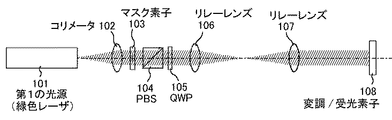
ホログラフィックメモリについては、例えば非特許文献1において解説がなされている。図15は、ホログラフィックメモリによる従来の記録再生装置であって、コリニア方式と呼ばれる同軸タイプのホログラフィックメモリシステム(光情報記録再生装置)の光学系を説明している。
The holographic memory is explained in, for example, Non-Patent
この光情報記録再生装置は、例えばディスク状であるホログラム記録媒体216に対して情報の記録及び再生を行うものである。具体的には、情報によって変調された信号光と情報によっては変調されていない参照光とを同時に記録媒体216に照射して干渉させることによって、記録媒体216内に体積ホログラムを形成し、情報を記録する。また、弱い参照光を記録媒体216に照射することによって、体積ホログラムの再生像を取得し、情報を再生する。なお、体積ホログラムとは、記録媒体の体積ホログラムとは、記録媒体の厚み方向も積極的に利用し、3次元的に干渉縞を書き込む方式であり、厚みを増やすことで、回折効率を高め、多重記録を用いて記録容量を増大する方式である。デジタル体積ホログラムとは、体積ホログラムと同様の記録方式を用いつつも、記録する画像情報は2値化したデジタルパターンに限定したホログラム記録方式である。 This optical information recording / reproducing apparatus records and reproduces information on, for example, a disc-shaped hologram recording medium 216. Specifically, a volume hologram is formed in the recording medium 216 by simultaneously irradiating the recording medium 216 with signal light modulated by information and reference light not modulated by information to cause interference. Record. Further, by irradiating the recording medium 216 with weak reference light, a reproduction image of the volume hologram is acquired and information is reproduced. The volume hologram is a volume hologram of the recording medium, which is a method of actively using the thickness direction of the recording medium and writing interference fringes three-dimensionally. By increasing the thickness, the diffraction efficiency is increased. In this method, the recording capacity is increased by using multiple recording. The digital volume hologram is a hologram recording method in which image information to be recorded is limited to a binarized digital pattern while using a recording method similar to that of the volume hologram.
図示された光学系は、情報の記録及び再生に用いるレーザ光を発生する第1の光源201と、信号光を変調するための空間光変調素子(spacial light modulator;以下、SLMと略記する)204と、再生光を検出するための2次元の受光素子219を備えている。
The illustrated optical system includes a
[記録]
まず、上記光学系を用いて、ディスク状の記録媒体216に対して記録を行う場合について説明する。
[Record]
First, a case where recording is performed on a disk-shaped recording medium 216 using the optical system will be described.
緑色レーザ等からなる第1の光源201から出射された光束は、コリメータ202によって平行光束とされ、ミラー203を経由し、空間光変調素子204を照明する。図15に示したものでは、SLM204として、DMD(Deformable Mirror Device)が使用されている。このようなSLM204は、2次元に配置された多数の光変調素子(画素)を有し、各画素ごとに「0」、「1」を表わすことができるようになっている。SLM204において、「1」の情報を表わす画素で反射された光は、記録媒体216の方向へ反射され、「0」の情報を表わす画素で反射された光は記録媒体216の方向へ反射されない。コリニア方式のホログラフィックメモリシステムで用いられるSLM204では、その中央部分が、情報光206を変調する部分とされており、それを環状に取り巻く部分は、参照光205を変調する部分となっている。
The light beam emitted from the
SLM204において「1」の情報を表わす画素で反射された情報光206及び参照光205は、いずれも、偏光ビームスプリッタ(以下、PBSと略記する)207をP偏光で透過する。そして、第1のリレーレンズ208、ミラー209、第2のリレーレンズ210、ダイクロイックビームスプリッタ(以下、DBSと略記する)211を経由して記録媒体216に向けられる。DBS211の通過後、1/4波長板(以下、QWPと略記する)212を透過して円偏光(例えば、右回りの円偏光)に変換された参照光205と情報光206は、ミラー213で反射されて、焦点距離Fの対物レンズ214に入射する。SLM204上に表示されたパターンは、第1及び第2のリレーレンズ208、210により、対物レンズ214からFだけ手前に中間像を形成する。これにより、SLM204上のパターン像(図示せず)、対物レンズ214、記録媒体216がいずれもFの距離だけ離れて配置される、4F光学系が構成される。
Both the information beam 206 and the reference beam 205 reflected by the pixel representing the information “1” in the
ディスク状の記録媒体216は、スピンドルモータ215上に回転可能に保持されている。対物レンズ214によって、参照光205と情報光206は記録媒体216に集光され、干渉して干渉縞を形成する。記録媒体216中の高分子材料には、この記録時の干渉縞パターンが屈折率分布として記録され、その結果、デジタル体積ホログラムが形成される。SLM204により、記録すべき情報に応じて情報光206を変調すれば、記録媒体216に、その情報に応じたデジタル体積ホログラムが形成される。特に、SLM204の情報光領域において、記録すべき情報に応じて画素ごとに変調を行えば、記録媒体216に、そのような画素数に応じた情報量を有するデジタル体積ホログラムが形成されることとなる。なお、記録媒体216中には、反射膜が設けられている。
A disk-shaped recording medium 216 is rotatably held on a spindle motor 215. The reference light 205 and the information light 206 are collected on the recording medium 216 by the objective lens 214 and interfere to form interference fringes. On the polymer material in the recording medium 216, the interference fringe pattern at the time of recording is recorded as a refractive index distribution, and as a result, a digital volume hologram is formed. When the information light 206 is modulated by the
光情報記録再生装置には、ホログラム化された光情報の記録再生を行う第1の光源201以外に、記録媒体216に対する感光性のない赤色レーザ等からなる第2の光源220が設けられている。この第2の光源220を用いて、記録媒体216の反射膜を基準面として、記録媒体216の変位を高精度に検出することが可能である。これより、記録媒体216に面ブレや偏心が発生しても、光サーボ技術を用いてダイナミックに記録スポットを記録媒体面に追従させることが可能となり、高精度に干渉縞パターンを記録することができる。以下、このようなトラッキングについて、簡単に説明する。
In addition to the
赤色レーザ等からなる第2の光源220から出射された直線偏光光束は、ビームスプリッタ(以下、BSと略記する)221を透過し、レンズ222で平行光束とされ、ミラー223とDBS211で反射されて、記録媒体216に向けられる。QWP212を透過し、円偏光(例えば、右回りの円偏光)に変換された光束は、ミラー213で反射されて対物レンズ214に入射して、記録媒体216の反射膜に微小な光スポットとして集光される。反射された光束は逆回りの円偏光(例えば、左回りの円偏光)となり、対物レンズ214に再入射して平行光束とされ、ミラー213で反射されてQWP212を透過して、往路での偏光とは垂直な直線偏光光束に変換される。DBS211で反射された光束は、往路と同様にミラー223、レンズ222を経由し、BS221で反射されて、光検出器224に導かれる。光検出器224は、複数の受光面を有していて、反射面の位置情報を検知する、この検知結果に基づいて対物レンズ214のフォーカスとトラッキングを行うことができる。このようなフォーカス及びトラッキングは、CDやDVDなどを用いる従来からよく知られた光情報記録再生装置において行われるものと同様のものである。
A linearly polarized light beam emitted from the second light source 220 made of a red laser or the like is transmitted through a beam splitter (hereinafter abbreviated as BS) 221, converted into a parallel light beam by a
[再生]
次に、上記光学系を用いて、記録媒体216に記録されている情報の再生を行う場合について説明する。第1の光源201から出射された光束は、記録時と同様にSLM204を照明する。再生時は、SLM204の参照光205を変調する部分のみが「1」の情報を表示し、情報光206を変調する部分はすべて「0」の情報を表示する。したがって、参照光205の部分の画素で反射された光だけが、記録媒体216の方向へ反射され、情報光206は記録媒体216の方向へ反射されない。
[Regeneration]
Next, a case where information recorded on the recording medium 216 is reproduced using the optical system will be described. The light beam emitted from the
記録時と同様に参照光205は、円偏光(例えば、右回りの円偏光)となって記録媒体216に集光され、記録されている干渉縞(デジタル体積ホログラム)から情報光を再生する。記録媒体216中の反射膜で反射された情報光は、逆回りの円偏光(例えば、左回りの円偏光)となり、対物レンズ214に再入射して平行光束とされ、ミラー213で反射されてQWP212を透過して、往路での偏光とは垂直な直線偏光光束(S偏光)に変換される。この時、対物レンズ214からFの距離に再生されたSLM204の表示パターンの中間像が形成される。
As in the recording, the reference light 205 is circularly polarized (for example, clockwise circularly polarized light), collected on the recording medium 216, and information light is reproduced from the recorded interference fringes (digital volume hologram). The information light reflected by the reflective film in the recording medium 216 becomes reversely circularly polarized light (for example, counterclockwise circularly polarized light), reenters the objective lens 214 to become a parallel light beam, and is reflected by the mirror 213. The light passes through the
DBS211を透過した光束は、第2のリレーレンズ210、ミラー209、第1のリレーレンズ208を経由してPBS207に向けられる。PBS207で反射された光束は、SLM204と共役の位置に、SLM204の表示パターンの中間像として再結像される。この位置には開口217が予め置かれていて、情報光の周辺部にある不要な参照光が遮蔽される。そして、レンズ218により、再結像された中間像は、CMOSセンサ等の受光素子219上に、情報光の部分のみのSLM204の表示パターンを形成する。これにより、不要な参照光205が受光素子219に入射しないので、S/N(信号対ノイズ比)の良い再生信号が得られる。
The light beam that has passed through the DBS 211 is directed to the PBS 207 via the second relay lens 210, the
結局、この光情報記録再生装置では、記録すべき情報を2次元デジタルパターン情報に展開し、この2次元デジタルパターン情報によって情報光が変調される。この処理により、記録情報が2次元空間の光強度分布画像情報となった情報光が生成される。そして情報光と参照光とを干渉させることによって、その干渉縞が記録媒体に記録される。再生時には、参照光を照射する事で再生される光強度分布画像情報から2次元デジタルパターン情報を抽出し、デコードする。このデジタル処理により、S/N比の劣化による再生誤り率の低下を抑えることが可能となり、また、2値化データをコード化してエラー訂正を行うことで、極めて忠実に、記録情報を再現することが可能となる。 Eventually, in this optical information recording / reproducing apparatus, information to be recorded is developed into two-dimensional digital pattern information, and information light is modulated by this two-dimensional digital pattern information. By this processing, information light in which the recorded information becomes the light intensity distribution image information in the two-dimensional space is generated. Then, the interference fringes are recorded on the recording medium by causing the information light and the reference light to interfere with each other. At the time of reproduction, two-dimensional digital pattern information is extracted from the light intensity distribution image information reproduced by irradiating the reference light and decoded. This digital processing makes it possible to suppress a reduction in the reproduction error rate due to the deterioration of the S / N ratio, and reproduces recorded information with high fidelity by encoding binary data and performing error correction. It becomes possible.
上述したコリニア方式のホログラフィックメモリシステムでは、情報光と参照光とが角度を持たない同軸上の光学配置を有するので、1つの対物レンズを用いて記録再生を行うことができる。そのため、情報光と参照光とを別々の光路から記録媒体に照射させる2軸2光束干渉方式と比較して、光学系が簡単になるという利点を有する。また、反射膜を有する記録媒体の構造により、ディスク状の記録媒体の片面側に光学系を配置することができる利点を有する。
しかしながら、上述した従来のホログラフィックメモリシステムにおいては、2次元の空間光変調素子(SLM)とCMOSセンサなどからなる受光素子との間のシフト(位置ずれ)、チルト(傾き角)およびローテーション(回転角)を高精度に制御して両者を位置あわせ必要があるので、コスト低下が困難である。 However, in the above-described conventional holographic memory system, shift (position shift), tilt (tilt angle), and rotation (rotation) between a two-dimensional spatial light modulator (SLM) and a light receiving element such as a CMOS sensor. It is difficult to reduce the cost because it is necessary to control the angle) with high accuracy and to align the two.
本発明の目的は、ホログラフィックメモリシステムに代表される光情報記録再生装置において、空間光変調素子と受光素子との位置合わせ作業を不要とし、また、光学系のコストダウンとコンパクト化を可能とすることにある。 An object of the present invention is that an optical information recording / reproducing apparatus represented by a holographic memory system eliminates the need for alignment work between a spatial light modulation element and a light receiving element, and enables cost reduction and downsizing of an optical system. There is to do.
本発明の別の目的は、そのような光情報記録再生装置において情報光の変調と受光とに用いられる素子を提供することにある。 Another object of the present invention is to provide an element used for modulation and reception of information light in such an optical information recording / reproducing apparatus.
本発明の光情報記録再生装置は、情報光と参照光との干渉によって生じる干渉縞を記録媒体に形成することにより情報を記録媒体に記録するともに、干渉縞が形成された記録媒体に参照光を照射して情報の再生を行う光情報記録再生装置において、光源と、変調信号に応じて反射光の強度が変化する複数の変調素子を有し、光源から出射された光束の少なくとも一部を変調し情報光とするための空間光変調素子と、参照光と情報光を記録媒体の所定の深さで干渉させるための光学系と、光源から参照光を記録媒体の所定の深さに当てて、干渉縞から情報光を再生して再生された情報光を取り出す光学系と、2次元の受光素子と、取り出された情報光を受光素子へ導入する光学系と、を有し、空間光変調素子と受光素子とが同一の基板に一体的に形成されており、基板において受光素子の複数の画素を覆う層間絶縁膜上に複数の変調素子が配置されることによって空間光変調素子は基板の受光素子が形成される表面に配置されていることを特徴とする。 The optical information recording / reproducing apparatus of the present invention records information on a recording medium by forming interference fringes generated by interference between the information light and the reference light on the recording medium, and also uses the reference light on the recording medium on which the interference fringes are formed. In an optical information recording / reproducing apparatus that reproduces information by irradiating light , a light source and a plurality of modulation elements that change the intensity of reflected light according to a modulation signal are provided , and at least part of a light beam emitted from the light source A spatial light modulator for modulating information light, an optical system for causing the reference light and information light to interfere with each other at a predetermined depth of the recording medium, and applying the reference light from the light source to the predetermined depth of the recording medium. An optical system that reproduces information light from the interference fringes and extracts the reproduced information light; a two-dimensional light receiving element; and an optical system that introduces the extracted information light into the light receiving element. integrally on the same board and the modulation element and the light receiving element The spatial light modulation element is disposed on the surface of the substrate on which the light receiving element is formed by disposing the plurality of modulation elements on the interlayer insulating film that covers the plurality of pixels of the light receiving element on the substrate . It is characterized by that.
本発明の素子は、光源からの光を変調するとともに外部から入射する光を受光する素子において、変調信号に応じて反射光の強度が変化する複数の変調素子を有し、光源から出射された光束の少なくとも一部を変調し情報光とするための空間光変調素子と、外部から入射する光を受光する2次元の受光素子と、を有し、空間光変調素子と受光素子とが同一の基板に一体的に形成されており、基板において受光素子の複数の画素を覆う層間絶縁膜上に複数の変調素子が配置されることによって空間光変調素子は基板の受光素子が形成される表面に配置されていることを特徴とする。 The element of the present invention is an element that modulates light from a light source and receives light incident from the outside, and has a plurality of modulation elements in which the intensity of reflected light changes according to a modulation signal, and is emitted from the light source A spatial light modulation element for modulating at least a part of the light flux to be information light, and a two-dimensional light receiving element for receiving light incident from the outside, the spatial light modulation element and the light receiving element being the same are integrally formed on the base plate, the spatial light modulator by the plurality of modulating elements are disposed on the interlayer insulating film covering the plurality of pixels of the light receiving element in the substrate surface receiving element of the substrate is formed It is characterized by being arranged in .
本発明において、空間光変調素子と受光素子との位置関係としては、基板上に空間光変調素子と受光素子とを縦方向に配置するものと、横方向に配置するものとがある。縦方向に配置する場合には、空間光変調素子が光源側に配置されるように空間光変調素子と受光素子が積層され、空間光変調素子における画素ピッチと受光素子における画素ピッチとが一致して空間光変調素子における画素と受光素子における対応する画素とが光源から入射する光の軸に沿って配置され、空間光変調素子に入射した光の少なくとも一部が受光素子に向けて透過するようにする。この場合、空間光変調素子は、各画素において受光素子に対して一定の透過率を有するように変調の設定が可能であることが好ましい。これに対して横方向に配置する場合には、空間光変調素子と受光素子は、空間光変調素子における画素と受光素子における対応する画素とが、光源から入射する光の軸に沿って重ならないように、相互に隣接して配置するようにする。 In the present invention, the positional relationship between the spatial light modulation element and the light receiving element includes one in which the spatial light modulation element and the light receiving element are arranged on the substrate in the vertical direction and the other in the horizontal direction. When arranged in the vertical direction, the spatial light modulation element and the light receiving element are stacked so that the spatial light modulation element is arranged on the light source side, and the pixel pitch in the spatial light modulation element and the pixel pitch in the light receiving element coincide. The pixels in the spatial light modulation element and the corresponding pixels in the light receiving element are arranged along the axis of light incident from the light source so that at least part of the light incident on the spatial light modulation element is transmitted toward the light receiving element. To. In this case, it is preferable that the spatial light modulation element can be set to be modulated so that each pixel has a certain transmittance with respect to the light receiving element. On the other hand, when arranged in the horizontal direction, the spatial light modulation element and the light receiving element do not overlap along the axis of light incident from the light source, with the pixel in the spatial light modulation element and the corresponding pixel in the light receiving element. Thus, they are arranged adjacent to each other.
上述した本発明の光情報記録再生装置及びそれに用いられる素子において、変調素子としては、変調信号に応じて反射光の強度が変化する素子を用いることが好ましい。そのような変調素子は、例えば、光源からの光を反射する反射電極と、反射電極より光源側に空間を介して配置され、光源からの光に対してある割合で透過させ残りは反射する機能を有する半透過膜とを有し、反射電極と半透過膜との距離を制御することによって光源からの光の反射率が変化する素子である。あるいは変調素子は、反射型液晶素子である。 In the above-described optical information recording / reproducing apparatus of the present invention and the element used therefor, it is preferable to use an element whose reflected light intensity changes according to the modulation signal as the modulation element. Such a modulation element is, for example, a reflective electrode that reflects light from a light source, and a function that is disposed through a space closer to the light source than the reflective electrode, and transmits the light from the light source at a certain ratio and reflects the rest. and a semi-permeable membrane having a device reflectance of light changes from a light source by controlling the distance between the reflective electrode and the semi-transmissive film. Alternatively, the modulation element is a reflective liquid crystal element.
本発明において、基板としてはシリコン半導体基板を用いることが好ましい。 In the present invention, a silicon semiconductor substrate is preferably used as the substrate.
本発明によれば、従来は、空間光変調素子と受光素子とをシリコンプロセスによるチップとして別々に設けていたのに対し、そのようなシリコン半導体チップを2個から1個へ半減させることができる。空間光変調素子とCMOSセンサなどの受光素子とは、それらを製造するための半導体プロセスの各工程が、ほとんど同じであるので、工程数の増加を伴うことなく、これらの素子の機能を一度に作りこむことが可能である。その結果、光情報記録再生装置として、光学系をより簡単なものとすることが可能となって、設置面積を小さくすることができるようになる。また、記録媒体への書き込みと記録媒体からの読み出しとをほぼ同じ軸上で行うことができることから、書き込み用の光学系と読み出し用の光学系との間の位置ずれが本質的になくなり、両者間の光学系のずれの調整が不要になる。本発明によれば、このような特徴を有して低コストで製造できる光情報記録再生装置を提供できるようになるとともに、そのような光情報記録再生装置において好適に用いられる変調/受光素子を提供できる。 According to the present invention, the spatial light modulation element and the light receiving element are conventionally provided separately as chips by a silicon process, but the number of such silicon semiconductor chips can be halved from two to one. . Spatial light modulation elements and light-receiving elements such as CMOS sensors are almost the same in each process of the semiconductor process for manufacturing them, so that the functions of these elements can be performed at once without increasing the number of processes. It is possible to make it. As a result, the optical system can be simplified as an optical information recording / reproducing apparatus, and the installation area can be reduced. Further, since writing to the recording medium and reading from the recording medium can be performed on substantially the same axis, the positional deviation between the writing optical system and the reading optical system is essentially eliminated, and both It is not necessary to adjust the deviation of the optical system. According to the present invention, it is possible to provide an optical information recording / reproducing apparatus having such a feature that can be manufactured at low cost, and a modulation / light receiving element suitably used in such an optical information recording / reproducing apparatus. Can be provided.
次に、本発明の好ましい実施の形態について、図面を参照して説明する。 Next, a preferred embodiment of the present invention will be described with reference to the drawings.
(第1の実施形態)
まず、本発明の第1の実施形態の光情報記録再生装置について説明する。この光情報記録再生装置は、コリニア方式のホログラフィックメモリシステムとして構成されたものであり、空間光変調素子と、再生光を検出するためのCMOSイメージセンサなどの受光素子とを同一の半導体チップ上に形成したものである。図1〜図3は、本実施形態の光情報記録再生装置の光学系を説明する図である。図1は、記録時における光源から空間光変調素子までの光学系を示し、図2は、記録時における空間光変調素子からホログラムディスク(記録媒体)までの光学系を示し、図3は、再生時の光学系を示している。
(First embodiment)
First, an optical information recording / reproducing apparatus according to a first embodiment of the present invention will be described. This optical information recording / reproducing apparatus is configured as a collinear holographic memory system, and includes a spatial light modulation element and a light receiving element such as a CMOS image sensor for detecting reproduction light on the same semiconductor chip. Is formed. 1 to 3 are diagrams for explaining an optical system of the optical information recording / reproducing apparatus according to the present embodiment. FIG. 1 shows an optical system from a light source to a spatial light modulation element at the time of recording, FIG. 2 shows an optical system from the spatial light modulation element to a hologram disk (recording medium) at the time of recording, and FIG. The optical system of time is shown.
本実施形態の光情報記録再生装置は、例えばディスク状であるホログラム記録媒体186に対して、体積ホログラムの書き込みによって情報の記録を行い、体積ホログラムの再生像を取得することによって情報の再生を行うものである。図示された光学系は、情報の記録及び再生に用いるレーザ光を発生する第1の光源101と、信号光を変調するための空間光変調素子(SLM)と再生光を検出するための2次元の受光素子とを一体的に設けた変調/受光素子(SLM/CMOS)108とを備えている。
The optical information recording / reproducing apparatus of the present embodiment records information by writing volume holograms on, for example, a disk-shaped hologram recording medium 186, and reproduces information by acquiring reproduced images of volume holograms. Is. The illustrated optical system includes a first
本実施形態では、後述するように,変調/受光素子108における空間光変調素子部分としては、反射型光干渉変調素子を有する空間光変調素子を用い、受光素子としてはCMOSセンサを用いている。これら空間光変調素子とCMOSセンサとをシリコン半導体基板上で縦方向に積層して設けることにより、変調/受光素子108を構成している。この構成を用いることにより、空間光変調素子による光変調と受光素子による受光とを同軸で行うことができるようになっている。
In this embodiment, as will be described later, a spatial light modulation element having a reflection type interferometric modulation element is used as the spatial light modulation element portion of the modulation /
まず、図1及び2を用いて、ホログラムディスクである記録媒体118に記録を行う場合について説明する。図1において、緑色レーザ等からなる第1の光源101から出射された光束は、コリメータ102で平行光束とされ、マスク素子103に入射する。マスク素子103は、光束の中心部の情報光に相当する部分をマスクする働きを有する。マスク素子103としては、例えば液晶素子を用いることができる。光束の中心部を遮蔽するマスクを光路に挿入してもよい。情報の記録時には、このマスク素子103は機能せず、すべての光束を透過させている。マスク素子103を透過した光は、偏光ビームスプリッタ(以下、PBSと略記する)104に入射する。
First, the case of recording on the recording medium 118 which is a hologram disk will be described with reference to FIGS. In FIG. 1, a light beam emitted from a first
P偏光でPBS104を透過した光束は、必要に応じて設けられた1/4波長板(以下、QWPと略記する)105を透過し、第1のリレーレンズ106及び第2のリレーレンズ107を経由し、空間光変調素子(SLM)とCMOSセンサが1チップに搭載された変調/受光素子108に照射される。SLMとして偏光状態を変化させない構成の光干渉変調素子(iMOD)素子が用いられる場合には、QWP105を予め設ければよい。また、SLMとして偏光状態を90°変化させる構成の反射型液晶(LCOS;liquid crystal on silicon)素子の場合は、QWP105は不要である。ここで光干渉変調素子(iMOD)とは、反射電極と反射電極の前方に配置された半透過膜とを有する素子であり、半透過膜は、入射光をある割合で透過させ、残りは反射する機能を有する。この光干渉変調素子は、半透過膜側から光が入射した際の半透過膜表面からの反射光と、半透過膜を透過して反射電極によって反射された反射光との干渉を用いることによって、光変調を行う。反射電極も光を反射する性質を有し、ここで半透過膜と反射電極との間の空間の距離(エアギャップ)を変化させることによって、入射光の全体としての反射率を制御することができ、反射光の強度を変調することができる。エアギャップの距離は、半透過膜と反射電極との間に信号電圧を印加し、その信号電圧によって生じる電界によるクーロン力によって半透過膜を変位させることにより、制御することができる。半透過膜としてはTi(チタン)の薄膜を好ましく使用できる。
The light beam transmitted through the
以下、変調/受光素子108として、iMODとCMOSとの組み合わせからなる素子を用いる場合(iMOD/CMOS)と、LCOSとCMOSとの組み合わせからなる素子を用いる場合(LCOS/CMOS)とに分けて、記録動作を説明する。
Hereinafter, the modulation /
iMOD/CMOSの場合:
QWP105を透過した光束は、円偏光(例えば、右回りの円偏光)に変換され、第1のリレーレンズ106及び第2のリレーレンズ107を経由し、変調/受光素子108を照明する。変調/受光素子108のSLMで「1(白)」の情報を表わす画素によって反射された光は、高い反射率で記録媒体118の方向へ反射され、SLMの「0(黒)」の情報を表わす画素で反射された光は、干渉により記録媒体118の方向へはわずかしか反射されない。従来例と同様に、コリニア方式のSLMには、情報光110を変調する部分とそれを環状に取り巻く参照光109を変調する部分が設けられている。
For iMOD / CMOS:
The light beam transmitted through the
以下、図2によって説明すると、変調/受光素子108のSLMによって反射された光束は、逆回りの円偏光(例えば、左回りの円偏光)とされる。第2のリレーレンズ107及び第1のリレーレンズ106を経由した光束は、QWP105を透過してS偏光に変換され、PBS104で反射されて記録媒体118の方向に向けられる。
Hereinafter, referring to FIG. 2, the light beam reflected by the SLM of the modulation /
LCOS/CMOSの場合:
一方、変調/受光素子108としてLCOS/COMSが用いられる場合、PBS104を通過した光束は、第1のリレーレンズ106及び第2のリレーレンズB107を経由し、変調/受光素子108を照明する。SLM上で「1(白)」の情報を表わす画素で反射された光はS偏光に変換され、「0(黒)」の情報を表わす画素で反射された光はP偏光の状態を保持する。従来例と同様に、コリニア方式のSLM上には、情報光110を変調する部分とそれを環状に取り巻く参照光109を変調する部分が設けられている。
For LCOS / CMOS:
On the other hand, when LCOS / COMS is used as the modulation / light-receiving
以下、図2によって説明すると、変調/受光素子108で反射された光束のうち、S偏光はPBS104で反射されてホログラムディスク118の方向に差し向けられ、P偏光はPBS104を透過してホログラムディスク118の方向に向かわない。
Hereinafter, with reference to FIG. 2, among the light beams reflected by the modulation /
iMOD/CMOSを用いる場合も、LCOS/CMOSを用いる場合も、変調/受光素子108のSLMにおいて「1(白)」の情報を表わす画素によって反射された参照光109と情報光110は、PBS104で反射され、第3のリレーレンズ111、ミラー112、第4のリレーレンズ113、ダイクロイックビームスプリッタ(以下、DBSと略記する)114を経由して記録媒体118に向けられ、ミラー115で反射されて焦点距離Fの対物レンズ116に入射する。変調/受光素子108のSLMに表示されたパターンは、第3及び第4のリレーレンズ111、112により、対物レンズ116からFだけ手前に中間像を形成する。これにより、変調/検出素子108のSLM上のパターン像(不図示)、対物レンズ116、記録媒体118とがいずれもFの距離だけ離れて配置されている、4F光学系が構成されたことになる。
Whether using iMOD / CMOS or LCOS / CMOS, the reference light 109 and the information light 110 reflected by the pixel representing the information of “1 (white)” in the SLM of the modulation /
ディスク状の記録媒体118は、スピンドルモータ117上に回転可能に保持されている。対物レンズ116によって、参照光109と情報光110は記録媒体118に集光され、干渉して干渉縞を形成する。記録媒体118中の高分子材料には、この記録時の干渉縞パターンが屈折率分布として記録され、デジタル体積ホログラムが形成される。特に、記録すべき情報に応じて情報光110を変調すれば、記録媒体118に、その情報に応じたデジタル体積ホログラムが形成されることになる。なお、記録媒体118中には反射膜が設けられている。
A disk-shaped recording medium 118 is rotatably held on a
この光情報記録再生装置では、従来例のものと同様に、ホログラム化された光情報の記録再生を行う第1の光源101以外に、記録媒体118に対する感光性のない赤色レーザ等からなる第2の光源119が設けられている。この第2の光源119を用いて、記録媒体118の反射膜を基準面とし、記録媒体118の変位を高精度に検出することが可能である。これより、記録媒体118に面ブレや偏心が発生しても、光サーボ技術を用いてダイナミックに記録スポットを記録媒体面に追従させることが可能となり、高精度に干渉縞パターン(デジタル体積ホログラム)を記録することができる。以下に簡単に説明する。
In this optical information recording / reproducing apparatus, as in the conventional example, in addition to the first
第2の光源119から出射された光束は、ビームスプリッタ(以下、BSと略記する)120を透過し、レンズ121で平行光束とされ、ミラー122とDBS114で反射されて、記録媒体118に向けられる。その後、ミラー115で反射されて対物レンズ116に入射して記録媒体118の反射膜に微小な光スポットとして集光される。反射された光束は、対物レンズ116に再入射して平行光束とされ、ミラー115、DBS114で順次反射され、往路と同様にミラー122、レンズ121を経由し、ビームスプリッタBS120で一部の光束を反射されて、光検出器123に導かれる。光検出器123は、複数の受光面を有していて、公知の方法で反射面の位置情報を検知し、それに基づいて対物レンズ116のフォーカスとトラッキングを行うことができる。
A light beam emitted from the second
次に、図3を用いて、記録媒体118にデジタル体積ホログラムとして記録されている情報を再生する場合の動作を説明する。第1の光源101から出射された光束は、記録時と同様に、変調/受光素子108に照射される。この際、第1の光源101からの光の強さは、記録媒体118に記録されている情報を破壊しないように、記録時に用いられた強度よりも小さいものとされる。再生時において、マスク素子103は、光束の中心部の情報光に相当する部分をマスクする。本実施形態では、マスク素子103を構成する液晶素子は、光束の中心部のみ偏光方向を90°回転させてS偏光とし、後続のPBS104で反射させて変調/受光素子108に到達しないようにしている。また、中心部を遮蔽するマスクを光路に挿入してもよい。
Next, the operation for reproducing information recorded as a digital volume hologram on the recording medium 118 will be described with reference to FIG. The light beam emitted from the first
第1のリレーレンズ106及び第2のリレーレンズ107は、マスク素子103の像を変調/受光素子108のSLMに結像させる役目を有する。これにより、参照光の部分の素子のみが照明され、情報光の部分はマスク素子103の像によりきちんと遮光がなされることになる。変調/受光素子108のSLMにおいては、参照光109を変調する部分のみが「1(白)」の情報を表示し、情報光110を変調する部分は、すべて「0(黒)」の情報を表示する。したがって、参照光109を変調する部分の画素で反射された光だけが、記録媒体118の方向へ反射される。情報光110を反射する部分の画素の光束は、記録媒体118の方向へ反射されないばかりかもともと照明すらされないので、従来例と比較して、一段とS/Nの良い情報光の再生が可能となる。
The first relay lens 106 and the second relay lens 107 serve to form an image of the mask element 103 on the SLM of the modulation /
記録時と同様に参照光109は、PBS104で反射され、記録媒体118に集光され、記録された干渉縞から情報光を再生する。記録媒体118中の反射膜で反射された情報光(すなわち再生光)は、対物レンズ116に再入射して平行光束とされ、ミラー115で反射される。この時、対物レンズ116からFの距離に再生されたSLMの表示パターンの中間像が形成される。
As in the recording, the reference light 109 is reflected by the
DBS114を透過した光束は、第4のリレーレンズ113、ミラー112、第3のリレーレンズ111を経由してPBS104に向けられ、第4のリレーレンズ113と第3のリレーレンズ111とにより、マスク素子103と共役の位置にSLMの表示パターンの中間像として再結像される(図示せず)。そして、この再結像された中間像は、PBS104で反射され、第1のリレーレンズ106及び第2のリレーレンズ107により、変調/受光素子108上に結像される。なお、本実施形態では、受光素子として、画素ごとに、フォトダイオードとフォトダイオードで検出した受光信号を増幅するMOSトランジスタとを有する、CMOSセンサを用いている。しかも本実施形態では、変調/受光素子108として、空間光変調素子(SLM)とCMOSセンサなどの受光素子とを同一のチップ上に配したものを使用しているので、両者を位置合わせするためのの複雑な機構が不要となる。また、光学系のコストダウンとコンパクト化を図ることができる。
The light beam transmitted through the
次に、本実施形態の光情報記録再生装置における、記録・再生の回路動作を説明する。図4は、本実施形態において用いられた、反射型光干渉変調素子を用いたSLMとCMOSセンサからなる受光素子とを一体型とした変調/受光素子を説明するための等価回路図である。図4において、符号1〜10までは、空間光変調素子に係る構成要素に付与され、符号21〜33は、CMOSイメージセンサとして構成されている受光素子に係る構成要素の付与されている。
Next, the recording / reproducing circuit operation in the optical information recording / reproducing apparatus of the present embodiment will be described. FIG. 4 is an equivalent circuit diagram for explaining a modulation / light-receiving element in which an SLM using a reflection type interferometric modulation element and a light-receiving element made of a CMOS sensor are integrated, used in this embodiment. In FIG. 4,
列方向(図示垂直方向)に延びる複数の垂直信号線1,1a,…と、行方向(図示水平方向)に延びる複数の駆動線(走査線)2,2a,…とが設けられてこれらはマトリクス配線を構成しており、垂直信号線と駆動線との交点がそれぞれ画素に対応する。したがって、画素はマトリクス状に配置されていることになり、画素配列の列ごとに垂直信号線が設けられ、行ごとに駆動線が設けられていることになる。垂直信号線1,1a,…は空間光変調素子のためのものであり、これと同様に、列ごとに、受光素子のための垂直信号線26,26a,…が設けられている。さらに、行ごとに、受光素子のための水平読出し線27,27a,…、水平リセット線28,28a,…、水平選択線29,29a,…が設けられている。
Are provided with a plurality of
各画素には、空間光変調素子のために、スイッチングトランジスタからなる画素スイッチ3,3a,…と、干渉構造部4,4a,…と、保持容量5,5a,…が設けられている。また、各画素には、受光素子のために、フォトダイオード21,21a,…と、トランジスタからなる転送スイッチ22,22a,…と、トランジスタからなるリセットスイッチ23,23a,…と、増幅トランジスタ24,24a,…と、トランジスタからなる選択スイッチ25,25a,…とが設けられている。
Each pixel is provided with
各画素の空間光変調素子の部分では、画素スイッチ3,3a,…のゲートは対応する駆動線2,2a,…に接続し、ドレインは対応する垂直信号線1,1a,…に接続する。保持容量5,5a,…は、画素スイッチのソースと定電位点(例えば接地電位点)との間に設けられている。さらに、干渉構造部4,4a,…も画素スイッチのソースに接続している。各干渉構造部は、各画素に共通な共通対向電極6も備えている。垂直信号線1,1a,…の一端は、それぞれサンプリングスイッチ9,9a,…を介して空間光変調素子のための水平信号線10に接続し、サンプリングスイッチ9,9a,…のゲートは、区間光変調素子の水平シフトレジスタ8に接続する。また駆動線2,2a,…の一端は垂直シフトレジスタ7に接続する。
In the spatial light modulation element portion of each pixel, the gates of the pixel switches 3, 3a,... Are connected to the
ここで干渉構造部は、上述した反射電極と半透過膜とを備えるものであり、半透過膜は共通対向電極6として各画素に共通に設けられている。一方、反射電極は、画素ごとに画素スイッチのソースに接続されている。 Here, the interference structure section includes the above-described reflective electrode and the semi-transmissive film, and the semi-transmissive film is provided in common to each pixel as the common counter electrode 6. On the other hand, the reflective electrode is connected to the source of the pixel switch for each pixel.
各画素の受光素子の部分では、フォトダイオード21,21a,…のアノードは接地され、カソードはそれぞれ転送スイッチ22,22a,…の一端に接続している。転送スイッチ22,22a,…のゲートは対応する水平読出し線に接続し、他端はリセットスイッチの一端に接続している。リセットスイッチ23,23a,…は、フォトダイオード及びそれに対して電気的に接続するフローティングディフュージョン(FD)領域を所定電位までリセットするためのものであって、他端には所定の電位が印加されるとともに、ゲートは水平リセット線に接続している。さらに、転送スイッチ22,22a,…の他端は、フォトダイオード21,21a,…による信号電荷を増幅するための増幅トランジスタ24,24a,…のゲートにも接続している。増幅トランジスタ24,24a,…の一端には所定電位が印加され、他端は、選択スイッチ25,25a,…を介して、受光素子の対応する垂直信号線に接続する。選択スイッチのゲートは、対応する水平選択線に接続する。受光素子の垂直信号線26,26a,…の一端は、サンプリングスイッチ32,32a,…を介して、受光素子の水平信号線33に接続する。サンプリングスイッチ32,32a,…のゲートは、受光素子の水平シフトレジスタ31に接続する。受光素子のための水平読出し線27,27a,…、水平リセット線28,28a,…、水平選択線29,29aの各一端は、いずれも、受光素子の垂直シフトレジスタ30に接続している。
In the light receiving element portion of each pixel, the anodes of the
図4では、2行2列で画素が配置しているが、当然のことながら、本実施形態の光情報記録再生装置における変調/受光素子108の回路は、例えば1000行1000列のような多画素のマトリクス構成とすることもできる。
In FIG. 4, pixels are arranged in 2 rows and 2 columns, but it goes without saying that the circuit of the modulation /
本実施形態の変調/受光素子108の回路動作について説明する。まず、書き込みモードについて説明する。書き込み時の動作は、一般の表示装置などにおけるアクティブマトリクス動作と同様の動作である。
The circuit operation of the modulation /
まず垂直シフトレジスタ7から駆動線2にオン信号が入力され、画素スイッチ3,3aがオン状態になる。この状態で、水平シフトレジスタ8が順次動作し、水平信号線10から垂直信号線1に信号を伝達する。すなわち、まずサンプリングスイッチ9がオンになって、垂直信号線1に水平信号線10の信号が書き込まれ、画素スイッチ3を通して保持容量5に信号に応じた電荷が蓄積される。SLMとして反射型光干渉変調素子を用いる場合、干渉構造部4の反射電極(不図示)と共通対向電極6との間の電位差が印加され、この間に電界が生じる。この電界により、干渉構造部4を変化させ、具体的には反射電極と共通対向電極6との距離が変化し、入射光に対する反射率を所望の値に変調させることができる。ここで、SLMとしてLCOSが用いられるのであれば、液晶画素の一方の電極を画素スイッチに接続し他方を共通対向電極6とすればよい。LCOSを用いる場合であれば、液晶部に電界が生じ、この電界により液晶の配向が変化して、入射光の偏光特性を変化させる。偏光板・波長板等の組み合わせにより反射率を所望の値に変調させる。ホログラフィックメモリシステムにおけるSLMとしては白と黒の2階調があればよいので、反射率としては最大反射率あるいは最小反射率が得られる電圧を干渉構造部4または液晶部に与えることになる。
First, an ON signal is input from the vertical shift register 7 to the
次いでサンプリングスイッチ9をオフにした後にサンプリングスイッチ9aをオンにして、今度は、水平信号線10の信号を垂直信号線1aに書き込み、この信号を、画素スイッチ3aを介して保持容量5aに書き込む。このようなシーケンスで、水平方向(行方向)に順次信号を画素に書き込んでいく。
Next, the
1行全て書き込んだ後に、駆動線2がオフにされ、今度は駆動線2aに、画素スイッチ3b、3cをオン状態にするべく信号が入力される。後は前述同様に、水平方向に順次画素に信号を書き込んでいく。すべての行に電圧を書きこんだ後に、再びこの動作を第一行から繰り返し、各画素の電圧を書き換えていく。このようにして全画素に信号を書き込んだ後、第1の光源101からの光を変調/受光素子108に入射させれば、それぞれの画素において変調された光として反射し、その反射光は、参照光109と干渉して記録媒体118に記録される。
After all the lines have been written, the
変調/受光素子108において、参照光109を変調する画素、すなわち参照光領域にある画素は、一定の反射率になるように設定される。例えば、情報光が当たる画素と同じ構造にして、最大反射率が得られるような電圧を与える。また例えば、反射型光干渉変調素子を用いる場合には、干渉構造は形成せずに、単純にミラー構造としてもよい。
In the modulation /
次に、読出しモードについて説明する。 Next, the reading mode will be described.
記録媒体118に記録された情報が参照光109により再生され、受光画素に「1」(白)あるいは「0」(黒)に相当する光強度が入射され、それに応じた量の電荷がフォトダイオード21,21a…に蓄積される。垂直シフトレジスタ30から水平読出し線27にオン信号を出力し、転送スイッチ22をオン状態にすることで、フォトダイオードに貯められた電荷が増幅トランジスタ24のゲートの電位を変化させ、その結果、フォトダイオードに蓄えれた信号に応じた電圧が増幅トランジスタ24のドレインに出力される。垂直シフトレジスタ30から水平選択線29によって選択スイッチ25をオン状態にすると、増幅トランジスタ24の出力が垂直信号線26に伝達する。水平シフトレジスタ31を順次動作させて、サンプリングスイッチ32をオンにすることにより、垂直信号線26から水平信号線33へ情報が送られる。サンプリングスイッチ32をオフにした後、次列のサンプリングスイッチ32aがオンとなって、同様に信号が送られる。1行すべての信号が送られた後は、垂直シフトレジスタ30により、次の行に移行し、同様にして、順次、信号が読み出される。あとは読み出された信号に基づいて、記録媒体118に記録されている信号を再生すればよい。
Information recorded on the recording medium 118 is reproduced by the reference light 109, light intensity corresponding to “1” (white) or “0” (black) is incident on the light receiving pixel, and an amount of electric charge corresponding to the light intensity is applied to the photodiode. Are accumulated in 21, 21 a. An on signal is output from the
なお、反射型光干渉光変調素子を用いたSLMと受光素子であるCMOSセンサとをシリコン基板上に積層して一体化した場合、受光素子も干渉構造部の上述した半透過膜の下側に位置することになる。したがって、読出しモードを行う直前に、情報を受光するすべての画素のSLMのトランジスタ3、3a、3b、…を一度オン状態にして、干渉構造部4,4a,4b,…が同程度の透過率を示す状態に保持しておく必要がある。
In addition, when the SLM using the reflection type optical interference light modulation element and the CMOS sensor as the light receiving element are laminated and integrated on the silicon substrate, the light receiving element is also below the above-described semi-transmissive film of the interference structure portion. Will be located. Therefore, immediately before the read mode is performed, the
なお、図4に示す回路図は、空間光変調素子と受光素子とを縦方向に積層して一体型にした場合だけでなく、画素ごとに光変調素子と受光素子とを重ねることなく隣接させた場合にも、共通して適用できるものである。 Note that the circuit diagram shown in FIG. 4 is not limited to the case where the spatial light modulation element and the light receiving element are stacked in the vertical direction to be integrated, but the light modulation element and the light receiving element are adjacent to each other without overlapping. In this case, it can be applied in common.
次に、本実施形態における反射型光干渉光変調素子を用いたSLMと受光素子であるCMOSセンサとを縦に一体化にした、すなわち積層した変調/受光素子の構造について説明する。図5はそのような変調/受光素子の要部の断面構造を示している。ここでは、2画素分の領域が示されている。受光素子として高速読み出しが可能なCMOSセンサを用いる例を説明しているが、受光素子の種類は特に限定されるものではなく、CCDやその他の光センサでもよい。なお再生時には情報光の領域でのみ光学的な像パターンを検出すればよいので、受光素子は、SLMにおける情報光領域にのみ形成されるようにしてもよい。 Next, the structure of the modulation / light-receiving element in which the SLM using the reflection type optical interference light modulation element and the CMOS sensor as the light-receiving element in the present embodiment are vertically integrated, that is, is described. FIG. 5 shows a cross-sectional structure of the main part of such a modulation / light-receiving element. Here, a region for two pixels is shown. Although an example in which a CMOS sensor capable of high-speed reading is used as the light receiving element has been described, the type of the light receiving element is not particularly limited, and may be a CCD or other optical sensor. Since it is only necessary to detect an optical image pattern only in the information light region during reproduction, the light receiving element may be formed only in the information light region in the SLM.
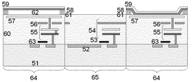
単結晶シリコン(Si)基板51の表面にフォトダイオード52が形成され、また、CMOSセンサの転送スイッチのゲート電極53が設けられている。これらの全面を覆うように層間絶縁膜60が設けられ、層間絶縁膜60内には、CMOSセンサの配線54、SLMの配線55及び遮光膜56が設けられている。遮光膜56は、入射光が下部トランジスタ領域に届かないようにするためのものである。そして層間絶縁膜60の最表面近くには、反射電極57が設けられている。配線54は、コンタクトホールを介して転送スイッチのソース/ドレイン電極と接続し、配線55はコンタクトホールを介して反射電極57に接続する。層間絶縁膜60の表面であって、反射電極57の周縁部にあたる位置には、支柱状の絶縁膜61が設けられており、この絶縁膜61に保持されるようにして、半透過膜58が設けられている。半透過膜58と反射電極57との間には、空間(エアギャップ)62が形成されている。半透過膜58の表面のうち、空間62に面しない方の表面の全面に保護膜59が形成されている。この図では、素子間絶縁するためのLOCOS酸化膜等や、CMOSセンサの他のトランジスタ、配線、SLMの画素スイッチや配線は省略してある。
A
この変調/受光素子では、入射光に対して反射電極(第1の干渉ミラー)57と半透過膜(第2の干渉ミラー)58との間で干渉を生じさせ、その間の空間(例えば空気)62の距離(エアギャップ)を変化させることで、反射率及び透過率を変化させている。この構成では、反射型光干渉光変調素子を用いたSLMと受光素子であるCMOSセンサを縦に一体化した構成となっている。そのため、受光素子であるCMOSセンサに入射する光を読み取る際に透過モードも使用するため、両方の干渉ミラー(すなわち半透過膜68及び反射電極57)とも半透明である必要がある。しかしながら、横配置の場合には、干渉構造部4では透過モードを使用する必要が無いので、反射電極57は半透明である必要はない。反射電極57が半透明でない場合には、反射電極57として、反射率の高い材料を用いることが好ましく、例えば、Al,AlSi,AlCu,Ti,Ta,W、Ag、Pt、Ru,Ni,Au,TiN等の金属膜、あるいはこれら金属の化合物膜を用いることができる。ただし、反射電極の材質はここに示したものに限定されるものではない。反射電極57と半透過膜58との間に配置された支柱状の絶縁膜61は、例えばシリコン窒化膜で形成され、半透過膜58の保護膜59は、例えばシリコン酸化膜で形成される。なお、支柱状の絶縁膜61、層間絶縁膜60、保護膜59としては、電気的な絶縁材料であれば特に限定されることなく使用することができ、またこれらを異なる材料で構成しても同じ材料で構成してもよい。
In this modulation / light receiving element, interference is generated between the reflective electrode (first interference mirror) 57 and the semi-transmissive film (second interference mirror) 58 with respect to incident light, and the space (for example, air) therebetween The reflectance and transmittance are changed by changing the distance 62 (air gap). In this configuration, an SLM using a reflective optical interference light modulation element and a CMOS sensor as a light receiving element are vertically integrated. Therefore, since the transmission mode is also used when reading the light incident on the CMOS sensor as the light receiving element, both interference mirrors (that is, the
次に、この変調/受光素子の干渉構造部としての動作について説明する。まずTiからなる半透過膜58には、例えば0Vのグランド電位を与える。前述したアクティブマトリクス動作により、反射電極57には、信号に応じた電圧が与えられ、反射電極57と半透過膜58との間に電位差が生じ、それによって発生するクーロン力によりエアギャップが変化する。図示上側から光が入射したとすると、その入射光のある割合の部分は半透過膜58の表面で反射され、残りの部分は半透過膜58を透過して反射電極57で反射され、半透過膜58を透過して外部に出射する。このとき、半透過膜58の表面で反射された成分と反射電極57で反射された成分とが干渉し、両者の位相差に応じて全体としての反射光の強度が変化する。位相差は光路差で決まり、光路差はエアギャップの大きさの2倍であるから、信号電圧に応じてエアギャップが変化させることにより、干渉構造部としての反射光(全体としての反射光)の強度を制御することができる。
Next, the operation of the modulation / light receiving element as an interference structure will be described. First, for example, a ground potential of 0 V is applied to the
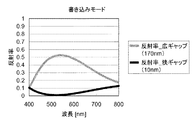
図6は、このように干渉構造部を構成した場合に、エアギャップが170nmの時と10nmの時での反射率の波長変化を表わしたグラフである。ここでは、保護膜59として厚さ10nmのSiO2を用い、半透過膜58としては、厚さ5nmのTiと厚さ20nmのSi3N4と厚さ10nmのSiO2と厚さ20nmのSi3N4をこの順で積層したものを用い、反射電極57としては、表面に厚さ10nmのSiO2膜を有する厚さ15nmのTiを用いた。図6に示すように、波長550nmの光において、エアギャップが170nmの時の反射率は52.5%であり、10nmの時の反射率は、1.2%である。反射電極57に与える信号の電圧により、エアギャップを10nmから170nmへと変化させると、それに伴い反射率が大きく変化することが分かる。この干渉作用は、波長や半透過膜材料、エアギャップによりそれぞれ設計可能であり、したがって、物理的な強度やコントラスト比等の特性を鑑みて、干渉構造部として必要な構成をとることが重要である。
FIG. 6 is a graph showing the change in the wavelength of the reflectance when the air gap is 170 nm and when the air gap is 10 nm when the interference structure is configured in this way. Here, SiO 2 having a thickness of 10 nm is used as the
読出しモードの場合には、少なくとも情報光が入射する画素では、光干渉の状態は同じ状態にして透過率を一定にしておく必要がある。そこでこの変調/受光素子においてエアギャップを10nmにした場合の透過率に波長変化を図7に示す。この場合、透過率は23.0%と比較的低いが、一定であることが重要であって透過率の絶対値はそれほど重要ではない。透過率を一定に保つことにより、再生光の強度をCMOSセンサで判別し、白画素なのか黒画素なのかを識別することが可能になる。 In the readout mode, it is necessary to keep the light transmittance constant and the transmittance constant in at least the pixels on which information light is incident. Accordingly, FIG. 7 shows a change in wavelength in transmittance when the air gap is set to 10 nm in this modulation / light receiving element. In this case, the transmittance is relatively low at 23.0%, but it is important that the transmittance is constant, and the absolute value of the transmittance is not so important. By keeping the transmittance constant, it is possible to determine the intensity of the reproduction light with a CMOS sensor and identify whether it is a white pixel or a black pixel.
次に、このような反射型光干渉変調素子からなる空間光変調素子(SLM)とCMOSセンサである受光素子とを一体化させた変調/受光素子の作成方法について説明する。 Next, a method for producing a modulation / light receiving element in which a spatial light modulation element (SLM) composed of such a reflection type interferometric modulation element and a light receiving element as a CMOS sensor are integrated will be described.
シリコン(Si)半導体基板を用い、この半導体基板上に、周知の方法によって、CMOSセンサを形成する。具体的な形成方法としては、任意のものを用いることができる。同時に、nMOSトランジスタによって、SLMの書き込み用のトランジスタ(図4における画素スイッチ3,3a,…)を形成する。その後、層間絶縁膜を形成し、各配線を形成し、さらに、反射型光干渉変調素子を形成する。具体的な作成手順の一例は以下のようなものである。 A silicon (Si) semiconductor substrate is used, and a CMOS sensor is formed on the semiconductor substrate by a known method. As a specific forming method, any method can be used. At the same time, SLM writing transistors (pixel switches 3, 3a,... In FIG. 4) are formed by nMOS transistors. Thereafter, an interlayer insulating film is formed, each wiring is formed, and further, a reflection type interferometric modulation element is formed. An example of a specific creation procedure is as follows.
n型単結晶シリコン半導体基板を部分熱酸化し、LOCOS(Local Oxdation of silicon)酸化膜を形成する。ついでLOCOS酸化膜をマスクとして、ボロン(B)をドーズ量1011 cm-2程度でイオン注入し、p型不純物領域であるp型ウエルを形成する。この基板を再度熱酸化し、厚さ60nmのゲート酸化膜を形成する。 The n-type single crystal silicon semiconductor substrate is partially thermally oxidized to form a LOCOS (Local Oxdation of silicon) oxide film. Next, boron (B) is ion-implanted with a dose of about 10 11 cm −2 using the LOCOS oxide film as a mask to form a p-type well which is a p-type impurity region. This substrate is thermally oxidized again to form a gate oxide film having a thickness of 60 nm.
次に、リン(P)を1020 cm-3程度ドープしたn形型ポリシリコンからなるゲート電極53を形成した後、基板全面にリンをドーズ量1013 cm-2程度でイオン注入し、不純物濃度1018 cm-3程度のn形不純物領域であるn型低濃度ドレインを形成する。引き続き、パターニングされたフォトレジストをマスクとして、リンをドーズ量1015 cm-2程度でイオン注入し、不純物濃度1020 cm-3程度のソース・ドレイン領域を形成し、nMOSトランジスタを形成する。同様にpMOSトランジスタを形成する。
Next, after forming a
CMOSセンサは、公知の手法で作成される。CMOSセンサを構成するトランジスタは、上記のトランジスタの形成工程と同時に形成可能であり、さらに、フォトダイオードの工程を付加するのみでよい。 The CMOS sensor is created by a known method. The transistors constituting the CMOS sensor can be formed at the same time as the above-described transistor forming process, and only a photodiode process is added.
その後、基板全面に層間絶縁膜60を形成する。層間絶縁膜には、PSG(Phospho-silicate Glass)膜やNSG(Nondope Silicate Glass)/BPSG(Boro-Phospho-Silicate Glass)膜、あるいは、TEOS(テトラエトキシシラン)によるCVD(化学気相成長)膜等を用いることが可能であり、特に限定されるものではない。
Thereafter, an
次に、ソース・ドレイン領域の直上にコンタクトホールをパターニングし、スパッタリング等によりアルミニウム(Al)層を蒸着した後パターニングし、下地の配線54を形成する。この下地配線層334と、ソース・ドレイン領域とのオーミックコンタクト特性を向上させるために、Ti/TiN等のバリアメタルを配線54とソース・ドレイン領域との間に形成することが望ましい。その後、層間絶縁膜を形成し、さらに金属膜によって遮光膜56を形成する。遮光膜56には、例えばTi、TiN、Al、Ag等の金属膜もしくはそれらの積層膜を用いることができ、特に限定されるものではない。遮光膜56をパターニングした後、さらに層間絶縁膜60を形成し、配線55上の所定の位置にコンタクトホールを設けてプラグを形成する。次いで、プラグにタングステンを堆積した後にCMP(化学機械研磨)法により平坦化する。
Next, a contact hole is patterned immediately above the source / drain region, an aluminum (Al) layer is deposited by sputtering or the like, and then patterned to form a
その後、Tiをスパッタ法などによりおよそ厚さ15nm堆積し、パターニングして反射電極57を形成する。次いで、CVD法により、反射電極57の保護膜として厚さ15nmのシリコン酸化膜を設ける。
Thereafter, Ti is deposited to a thickness of about 15 nm by sputtering or the like, and patterned to form the
次に、シリコン窒化膜をプラズマCVD法により形成し、パターニング後のエッチングにより、支柱状の絶縁膜61を形成する。その後、レジストを塗布し平坦化した後に、およそ高さ180nmの支柱状の絶縁層61が均一に残るように平坦化する。次に、低温のスパッタ法により、Si3N4:厚さ20nm、SiO2:厚さ10nm、Si3N4:厚さ20nm、Ti:厚さ5nmを順次形成し、さらに、保護膜59となるシリコン酸化膜を厚さ10nm堆積させた。パターニングした後にドライもしくはウエットエッチングでシリコン窒化膜、シリコン酸化膜及びTi層をエッチングし、その後レジストをウエットエッチングにより除去する。この工程により、半透過膜58と保護層59が形成される。その後、ワイアボンディングで電極を取り出して、反射型光干渉変調素子が完成する。
Next, a silicon nitride film is formed by plasma CVD, and a columnar insulating
(第2の実施形態)
上述した第1の実施形態では、シリコン半導体基板の表面において空間光変調素子(SLM)と受光素子(CMOSセンサ)とを縦方向に積層していたが、本発明はこれに限定されるものではない。変調/受光素子108において、画素ごとに、空間光変調素子と受光素子とを横置きに配置してもよい。図8は、このようにSLMと受光素子とが横置きに配置された変調/受光素子108を示している。
(Second Embodiment)
In the first embodiment described above, the spatial light modulation element (SLM) and the light receiving element (CMOS sensor) are stacked in the vertical direction on the surface of the silicon semiconductor substrate. However, the present invention is not limited to this. Absent. In the modulation /
図8に示す変調/受光素子108は、画素ごとに、反射型光干渉変調素子からなるSLMを有するSLM素子領域64と、CMOS受光素子を有するCMOSセンサ領域65と、を備えている。画素ごとのSLM素子領域64とCMOSセンサ領域65は、同一のシリコン基板51に設けられて相互に隣接して配置している。
The modulation / light-receiving
図8に示すような変調/受光素子の製造プロセスは、基本的には、第1の実施形態で示した縦配置の変調/受光素子の製造プロセスと同様のものである。すなわち、SLM素子領域64には、フォトダイオードは設けられないが、反射電極57と半透過膜58とからなる干渉構造が形成される。一方、CMOSセンサ領域65では、干渉構造は形成されないが、フォトダイオード52は形成される。図示していないが、この構造においては、CMOSセンサ領域65上にマイクロレンズを配置すると、実効的な開口率が増加する。
The manufacturing process of the modulation / light receiving element as shown in FIG. 8 is basically the same as the manufacturing process of the vertically arranged modulation / light receiving element shown in the first embodiment. That is, although no photodiode is provided in the
このような横配置の変調/受光素子の場合、SLMを構成する反射型光干渉変調素子において、受光素子に光を導くための透過モードは必要としないので、反射電極57として、アルミニウム(Al)などからなる比較的厚い膜を使用することができる。 In the case of such a laterally arranged modulation / light-receiving element, the reflection type interferometric modulation element constituting the SLM does not require a transmission mode for directing light to the light-receiving element. It is possible to use a relatively thick film made of, for example.
図9は、このように干渉構造部を構成した場合に、エアギャップが180nmの時と10nmの時での反射率の波長変化を表わしたグラフである。ここでは、保護膜59として厚さ10nmのSiO2を用い、半透過膜58としては、厚さ5nmのTiと厚さ20nmのSi3N4と厚さ10nmのSiO2と厚さ20nmのSi3N4をこの順で積層したものを用い、反射電極57としては、表面に厚さ10nmのSiO2膜を有する厚さ15nmのAlSiを用いた。図6に示すように、波長550nmの光において、エアギャップが180nmの時の反射率は93.0%であり、10nmの時の反射率は、0.6%である。反射電極57に与える信号の電圧により、エアギャップを10nmから180nmへと変化させると、それに伴い反射率が大きく変化することが分かる。この干渉作用は、波長や半透過膜材料、エアギャップによりそれぞれ設計可能であり、したがって、物理的な強度やコントラスト比等の特性を鑑みて、干渉構造部として必要な構成をとることが重要である。
FIG. 9 is a graph showing a change in the wavelength of the reflectance when the air gap is 180 nm and when the air gap is 10 nm when the interference structure portion is configured in this way. Here, SiO 2 having a thickness of 10 nm is used as the
(第3の実施形態)
本発明において、空間光変調素子として用いられるものは、上述した反射型光干渉変調素子に限られるものではない。図10に示すものは、空間光変調素子として反射型液晶素子(LCOS)を用い、変調/受光素子において反射型液晶素子とCMOS(センサ)とを縦方向に配列したものである。
(Third embodiment)
In the present invention, what is used as the spatial light modulation element is not limited to the above-described reflection type interferometric modulation element. In FIG. 10, a reflective liquid crystal element (LCOS) is used as the spatial light modulator, and the reflective liquid crystal element and the CMOS (sensor) are arranged in the vertical direction in the modulation / light receiving element.
シリコン基板51の表面にフォトダイオード52や転送スイッチのゲート電極53が設けられるともに、その上に層間絶縁膜60が設けられ、層間絶縁膜60中に配線54,55や遮光膜56が設けられることは、図5に示した変調/受光素子と同様である。図10に示した変調/受光素子では、層間絶縁膜60の表面の近傍に、画素ごとの画素電極65が設けられている。層間絶縁膜60に対向してガラス板70が配置しており、層間絶縁膜60とガラス板70との間に、液晶68が封入されている。ガラス板70の液晶68側の表面には、共通電極となるITO(酸化インジウム・スズ)膜69が形成され、ITO膜69の表面及び層間絶縁膜60の表面には、配向膜67が設けられている。ここで液晶68としては垂直液晶が用いられ、配向膜67としては、斜方蒸着SiO2膜が用いられる。画素電極66は、例えば50%の反射率を有する、半透明膜として設けられている。なお、この変調/受光素子では、入射光(波長:λ)が液晶68を通過し画素電極66で反射され再び液晶68を通過した際にλ/2の位相のずれが生じるように、液晶68の組成と厚さとが設計されている。
A
このような変調/受光素子において、「1」表示では、画素電極66と共通電極69との間に電圧が印加され、液晶68に電界が加わり液晶分子が倒れる。一方、「0」表示では、電界が加わらず、液晶分子はほぼ垂直に立っている。このような反射型液晶素子を空間光変調素子として用いることとすると、図1及び図2に示したような光学系において、光入射前にPBS(偏光ビームスプリッター)104によってS偏光の直線偏光とされた光を変調/受光素子108に入射させると、「0」表示では、偏光方向が変わらずに画素電極で50%の強度で反射される。この場合、反射光が再度、PBS104に入るが、偏光が変化してないので、PBS104で反射されることとなり、その光は記録媒体(ホログラム)118へは到達しない。一方「1」表示の時は、画素電極66での反射率は50%であるが、上述したように液晶の組成と厚さが設定されているので、反射光は、偏光面が90°回転した直線偏光になる。したがってこの反射光は、PBS104にはP偏光で入って透過し、記録媒体118に向けられることになる。光の強度は「1」の場合でも50%になるが、「1」、「0」の判別のためには十分な強度である。
In such a modulation / light receiving element, in the “1” display, a voltage is applied between the
記録媒体118に記録されている情報の情報の読み出しの際は、情報光領域においては液晶68は単に再生光を透過させればよいので、液晶68の偏光状態はどのようであってもよく、液晶68はどのような状態であっても構わない。
When reading the information of the information recorded on the recording medium 118, the
(第4の実施形態)
反射型光干渉変調素子の場合と同様に、空間光変調素子として反射型液晶素子(LCOS)を用いる場合においても、画素ごとの空間光変調素子と受光素子とをシリコン基板上において横置きの配置とすることができる。図11は、そのような横置きの配置とした変調/受光素子を示している。
(Fourth embodiment)
As in the case of the reflection type interferometric modulation element, when the reflection type liquid crystal element (LCOS) is used as the spatial light modulation element, the spatial light modulation element and the light receiving element for each pixel are arranged horizontally on the silicon substrate. It can be. FIG. 11 shows a modulation / light-receiving element having such a horizontal arrangement.
図11に示す変調/受光素子は、画素ごとに、反射型液晶素子からなるSLMを有するSLM素子領域64と、CMOS受光素子を有するCMOSセンサ領域65と、を備えている。画素ごとのSLM素子領域64とCMOSセンサ領域65は、同一のシリコン基板51に設けられて相互に隣接して配置している。この変調/受光素子の空間光変調素子としての動作は、情報の記録を行う場合も、情報の再生を行う場合も、上述した縦配置の場合と同じである。
The modulation / light-receiving element shown in FIG. 11 includes, for each pixel, an
(第5の実施形態)
上述した第2及び第4の実施形態では、変調/受光素子において、画素ごとに空間光変調素子(SLM)と受光素子(CMOS)とをシリコン基板上において横置きの配置としている。以下、空間光変調素子と受光素子との平面配置関係の例について説明する。
(Fifth embodiment)
In the second and fourth embodiments described above, in the modulation / light-receiving element, the spatial light modulation element (SLM) and the light-receiving element (CMOS) are arranged horizontally on the silicon substrate for each pixel. Hereinafter, an example of a planar arrangement relationship between the spatial light modulation element and the light receiving element will be described.
図12に示したものは、SLM素子領域とCMOSセンサ領域とがいずれも同じ面積の正方形の平面形状を有する場合における、SLM素子領域とCMOSセンサ領域との平面配置を示している。ここでは、SLM素子領域とCMOSセンサ領域とが、市松模様に配置している。これに対し、図13及び図14は、いずれも、CMOSセンサ領域の面積をSLM素子領域の面積よりも大きくして受光感度を向上させる例を示している。図13では、SLM素子領域とCMOSセンサ領域との面積比が1:3程度となっており、図14では、4:9程度となっている。ここでは図示していないが、SLM素子領域をCMOSセンサ領域よりも大面積で設けるようにしてもよい。SLM素子領域とCMOSセンサ領域との面積比は、記録する際に必要な情報光の強度、再生時に必要な再生光の強度、途中の光路での減衰量等に基づいて、最適な値となるように設定すればよい。 FIG. 12 shows a planar arrangement of the SLM element region and the CMOS sensor region when both the SLM element region and the CMOS sensor region have a square planar shape with the same area. Here, the SLM element region and the CMOS sensor region are arranged in a checkered pattern. On the other hand, FIGS. 13 and 14 show examples in which the area of the CMOS sensor region is made larger than the area of the SLM element region to improve the light receiving sensitivity. In FIG. 13, the area ratio between the SLM element region and the CMOS sensor region is about 1: 3, and in FIG. 14, it is about 4: 9. Although not shown here, the SLM element region may be provided in a larger area than the CMOS sensor region. The area ratio between the SLM element area and the CMOS sensor area is an optimum value based on the intensity of information light necessary for recording, the intensity of reproduction light necessary for reproduction, the amount of attenuation in an intermediate optical path, and the like. It should be set as follows.
以上説明した本発明の各実施形態では、空間光変調素子と受光素子とを同一の半導体基板上に設けているので、空間光変調素子と受光素子とを別々のチップに設ける場合に比べ、シリコン半導体プロセスによって製造すべきチップの数を2個から1個へ半減させることができる。空間光変調素子の製造プロセスと受光素子の製造プロセスとは共通の工程を多く有するので、結局、工程数の増加を伴うことなく、空間光変調素子の機能と受光素子の機能とを一度に作りこむことが可能になり、トータルとしての工程数の削減が可能になる。また、これらの実施形態によれば、ホログラフィックメモリシステムとしての光学系の規模を小さくすることができ、ホログラフィックメモリシステムの設置面積を小さくすることができる。また、空間光変調素子と受光素子とを同軸、あるいはほぼ同軸に配置することができることから、これらの素子を位置合わせするための複雑な機構が不要になるとともに、両者間の光学系のずれの調整が不要になる。 In each of the embodiments of the present invention described above, the spatial light modulation element and the light receiving element are provided on the same semiconductor substrate. Therefore, silicon is less than when the spatial light modulation element and the light receiving element are provided on separate chips. The number of chips to be manufactured by the semiconductor process can be halved from two to one. Since the manufacturing process of the spatial light modulation element and the manufacturing process of the light receiving element have many common processes, the function of the spatial light modulation element and the function of the light receiving element are created at the same time without increasing the number of processes. It is possible to reduce the total number of processes. Further, according to these embodiments, the scale of the optical system as the holographic memory system can be reduced, and the installation area of the holographic memory system can be reduced. In addition, since the spatial light modulation element and the light receiving element can be arranged coaxially or substantially coaxially, a complicated mechanism for aligning these elements is not necessary, and the optical system is not displaced between the two. No adjustment is required.
1,26 垂直信号線
2 駆動線(走査線)
3 スイッチングトランジスタ
4 干渉構造部
5 保持容量
6 共通対向電極
7,30 垂直シフトレジスタ
8,31 水平シフトレジスタ
9,32 サンプリングスイッチ
10,33 水平信号線
21,52 フォトダイオード
22 転送スイッチ
23 リセットスイッチ
24 増幅トランジスタ
25 選択スイッチ
27 水平読出し線
28 水平リセット線
29 水平選択線
51 Si基板
52 フォトダイオード
53,63 ゲート電極
54,55 配線
56 遮光膜
57 反射電極
58 半透過膜
59 保護膜
60 層間絶縁膜
61 絶縁膜
62 空間
64 SLM素子領域
65 CMOSセンサ領域
66 画素電極
67 配向膜
68 液晶
69 ITO膜
70 ガラス板
101,201 第1の光源(緑色レーザ)
102,202 コリメータ
103 マスク素子
104,207 偏光ビームスプリッタ(PBS)
105,212 1/4波長板(QWP)
106,107,111,113,208,210 リレーレンズ
108 変調/受光素子
109,205 参照光
110,206 情報光
112,115,122,203,209,213,223 ミラー
114,211 ダイクロイックビームスプリッタ(DBS)
116,214 対物レンズ
117,215 スピンドルモータ
118,216 記録媒体
119,220 第2の光源(赤色レーザ)
120,221 ビームスプリッタ(BS)
121,218,222 レンズ
123,224 光検出器
204 空間光変調素子(SLM)
217 開口
219 受光素子
1,26
DESCRIPTION OF
102, 202 Collimator 103
105,212 1/4 wave plate (QWP)
106, 107, 111, 113, 208, 210
116, 214
120,221 Beam splitter (BS)
121, 218, 222
217 Aperture 219 Light-receiving element
Claims (14)
光源と、
変調信号に応じて反射光の強度が変化する複数の変調素子を有し、前記光源から出射された光束の少なくとも一部を変調し前記情報光とするための空間光変調素子と、
前記参照光と前記情報光を前記記録媒体の所定の深さで干渉させるための光学系と、
前記光源から前記参照光を前記記録媒体の所定の深さに当てて、前記干渉縞から前記情報光を再生して再生された情報光を取り出す光学系と、
2次元の受光素子と、
前記取り出された情報光を前記受光素子へ導入する光学系と、
を有し、前記空間光変調素子と前記受光素子とが同一の基板に一体的に形成されており、前記基板において前記受光素子の複数の画素を覆う層間絶縁膜上に前記複数の変調素子が配置されることによって前記空間光変調素子は前記基板の前記受光素子が形成される表面に配置されていることを特徴とする光情報記録再生装置。 Information is recorded on the recording medium by forming interference fringes generated by interference between the information light and the reference light on the recording medium, and information is reproduced by irradiating the recording medium on which the interference fringes are formed with the reference light. In the optical information recording / reproducing apparatus to perform,
A light source;
A spatial light modulator for modulating at least a part of a light beam emitted from the light source to form the information light, having a plurality of modulators that change the intensity of reflected light according to a modulation signal ;
An optical system for causing the reference light and the information light to interfere at a predetermined depth of the recording medium;
An optical system for extracting the reproduced information light by applying the reference light from the light source to a predetermined depth of the recording medium and reproducing the information light from the interference fringes;
A two-dimensional light receiving element;
An optical system for introducing the extracted information light into the light receiving element;
Has the has the spatial light modulator and the light receiving element is integrally formed on the same board, the plurality of modulation elements in the interlayer insulating film covering the plurality of pixels of the light receiving element in the substrate The optical information recording / reproducing apparatus is characterized in that the spatial light modulation element is arranged on a surface of the substrate on which the light receiving element is formed .
変調信号に応じて反射光の強度が変化する複数の変調素子を有し、前記光源から出射された光束の少なくとも一部を変調し前記情報光とするための空間光変調素子と、
前記外部から入射する光を受光する2次元の受光素子と、
を有し、
前記空間光変調素子と前記受光素子とが同一の基板に一体的に形成されており、前記基板において前記受光素子の複数の画素を覆う層間絶縁膜上に前記複数の変調素子が配置されることによって前記空間光変調素子は前記基板の前記受光素子が形成される表面に配置されていることを特徴とする素子。 In an element that modulates light from a light source and receives light incident from the outside,
A spatial light modulator for modulating at least a part of a light beam emitted from the light source to form the information light, having a plurality of modulators that change the intensity of reflected light according to a modulation signal ;
A two-dimensional light receiving element for receiving light incident from the outside;
Have
Wherein are integrally formed with the spatial light modulator and the light receiving element is the same board, the plurality of modulation elements are arranged on the interlayer insulating film on which the said substrate to cover the plurality of pixels of the light receiving element Thus, the spatial light modulation element is disposed on a surface of the substrate on which the light receiving element is formed .
Priority Applications (2)
| Application Number | Priority Date | Filing Date | Title |
|---|---|---|---|
| JP2005344377A JP4678852B2 (en) | 2005-11-29 | 2005-11-29 | Optical information recording / reproducing apparatus and element used therefor |
| US11/563,391 US7929191B2 (en) | 2005-11-29 | 2006-11-27 | Spatial light modulator and light sensing device provided on the same substrate |
Applications Claiming Priority (1)
| Application Number | Priority Date | Filing Date | Title |
|---|---|---|---|
| JP2005344377A JP4678852B2 (en) | 2005-11-29 | 2005-11-29 | Optical information recording / reproducing apparatus and element used therefor |
Publications (3)
| Publication Number | Publication Date |
|---|---|
| JP2007149263A JP2007149263A (en) | 2007-06-14 |
| JP2007149263A5 JP2007149263A5 (en) | 2009-01-22 |
| JP4678852B2 true JP4678852B2 (en) | 2011-04-27 |
Family
ID=38193346
Family Applications (1)
| Application Number | Title | Priority Date | Filing Date |
|---|---|---|---|
| JP2005344377A Expired - Fee Related JP4678852B2 (en) | 2005-11-29 | 2005-11-29 | Optical information recording / reproducing apparatus and element used therefor |
Country Status (2)
| Country | Link |
|---|---|
| US (1) | US7929191B2 (en) |
| JP (1) | JP4678852B2 (en) |
Families Citing this family (10)
| Publication number | Priority date | Publication date | Assignee | Title |
|---|---|---|---|---|
| WO2006098419A1 (en) * | 2005-03-16 | 2006-09-21 | Pioneer Corporation | Hologram recording/reproducing device and hologram recording method |
| JP4678853B2 (en) * | 2005-11-29 | 2011-04-27 | キヤノン株式会社 | Optical information recording / reproducing apparatus |
| US20080297311A1 (en) * | 2007-05-31 | 2008-12-04 | Wu Xing-Tao | Non-contact service providing systems |
| JP4914294B2 (en) | 2007-06-05 | 2012-04-11 | 富士重工業株式会社 | Horizontal axis windmill |
| US20090213303A1 (en) * | 2008-02-26 | 2009-08-27 | Himax Display, Inc. | Display apparatus and display substrate thereof |
| TWI409537B (en) * | 2008-04-03 | 2013-09-21 | Innolux Corp | Liquid crystal panel and liquid crystal display device using same |
| JP4471019B2 (en) * | 2008-04-15 | 2010-06-02 | ソニー株式会社 | Illumination device and display device |
| TWI496042B (en) * | 2009-07-02 | 2015-08-11 | Semiconductor Energy Lab | Touch panel and driving method thereof |
| CN103487839B (en) * | 2013-08-26 | 2015-12-09 | 中国科学院长春光学精密机械与物理研究所 | Equivalent detector abnormity pixel implementation method able to programme |
| CN112925140A (en) * | 2021-01-27 | 2021-06-08 | 豪威半导体(上海)有限责任公司 | LCOS display and electronic equipment |
Citations (3)
| Publication number | Priority date | Publication date | Assignee | Title |
|---|---|---|---|---|
| JP2003315692A (en) * | 2002-04-25 | 2003-11-06 | Fuji Photo Film Co Ltd | Image display element and method of manufacturing the same |
| JP2004272268A (en) * | 2003-03-10 | 2004-09-30 | Inphase Technologies Inc | Polytopic multiplex holography |
| WO2004102542A1 (en) * | 2003-05-13 | 2004-11-25 | Optware Corporation | Optical information recording/reproduction device and method |
Family Cites Families (5)
| Publication number | Priority date | Publication date | Assignee | Title |
|---|---|---|---|---|
| JP4044187B2 (en) * | 1997-10-20 | 2008-02-06 | 株式会社半導体エネルギー研究所 | Active matrix display device and manufacturing method thereof |
| US6747638B2 (en) * | 2000-01-31 | 2004-06-08 | Semiconductor Energy Laboratory Co., Ltd. | Adhesion type area sensor and display device having adhesion type area sensor |
| US7227540B2 (en) * | 2002-04-25 | 2007-06-05 | Fujifilm Corporation | Image display unit and method of manufacturing the same |
| JP2006220933A (en) * | 2005-02-10 | 2006-08-24 | Toshiba Corp | Optical information recording method and apparatus using holography |
| JP4678853B2 (en) * | 2005-11-29 | 2011-04-27 | キヤノン株式会社 | Optical information recording / reproducing apparatus |
-
2005
- 2005-11-29 JP JP2005344377A patent/JP4678852B2/en not_active Expired - Fee Related
-
2006
- 2006-11-27 US US11/563,391 patent/US7929191B2/en not_active Expired - Fee Related
Patent Citations (3)
| Publication number | Priority date | Publication date | Assignee | Title |
|---|---|---|---|---|
| JP2003315692A (en) * | 2002-04-25 | 2003-11-06 | Fuji Photo Film Co Ltd | Image display element and method of manufacturing the same |
| JP2004272268A (en) * | 2003-03-10 | 2004-09-30 | Inphase Technologies Inc | Polytopic multiplex holography |
| WO2004102542A1 (en) * | 2003-05-13 | 2004-11-25 | Optware Corporation | Optical information recording/reproduction device and method |
Also Published As
| Publication number | Publication date |
|---|---|
| JP2007149263A (en) | 2007-06-14 |
| US20070146847A1 (en) | 2007-06-28 |
| US7929191B2 (en) | 2011-04-19 |
Similar Documents
| Publication | Publication Date | Title |
|---|---|---|
| JP4678853B2 (en) | Optical information recording / reproducing apparatus | |
| JP4678852B2 (en) | Optical information recording / reproducing apparatus and element used therefor | |
| EP0881634B1 (en) | Optical head device | |
| JPH10124872A (en) | Optical information recording device and method, optical information reproducing device and method, and optical information recording medium | |
| US20070121468A1 (en) | Optical information recording and reproducing apparatus | |
| JP3812608B2 (en) | Optical information recording apparatus and method, optical information reproducing apparatus and method, and optical information recording medium | |
| US7746752B2 (en) | Servo controlling method of optical information processing apparatus and optical information recording and reproducing apparatus | |
| JP2002203334A (en) | Information reproducing and recording device for recording medium | |
| JP2001084637A (en) | Single objective lens optical pickup head | |
| JP4678854B2 (en) | Optical information recording / reproducing apparatus | |
| JP2008027490A (en) | Information recording and reproducing apparatus and information reproducing method | |
| JP4411375B2 (en) | Optical information recording apparatus and method, optical information reproducing apparatus and method, and optical information recording and reproducing apparatus and method | |
| JPH09120557A (en) | Optical pickup device | |
| JP2008052793A (en) | Recording medium, servo signal detecting method using the same, and information recording and reproducing apparatus | |
| JP2007149261A (en) | Optical information recorder, optical information recording and reproducing device, and optical information recording method | |
| JP2881734B2 (en) | Annular shutter mirror, method of manufacturing the same, and optical pickup device for heterogeneous optical disks using the same | |
| JP2007149264A (en) | Optical information processor and verification method | |
| JPH10293520A (en) | Optical information recorder and optical information reproducing device | |
| JP2007305207A (en) | Optical information recording and reproducing apparatus | |
| JP2007149254A (en) | Optical information recording/reproducing device | |
| JP4091484B2 (en) | Recording / playback device | |
| JP2005093048A (en) | Optical pickup device having spherical aberration correcting apparatus, and its spherical aberration correcting method | |
| US20070297031A1 (en) | Optical pickup device | |
| JP2007149252A (en) | Optical information recording/reproducing device | |
| JP2008123627A (en) | Optical information recording and reproducing apparatus |
Legal Events
| Date | Code | Title | Description |
|---|---|---|---|
| A521 | Request for written amendment filed |
Free format text: JAPANESE INTERMEDIATE CODE: A523 Effective date: 20081126 |
|
| A621 | Written request for application examination |
Free format text: JAPANESE INTERMEDIATE CODE: A621 Effective date: 20081126 |
|
| A977 | Report on retrieval |
Free format text: JAPANESE INTERMEDIATE CODE: A971007 Effective date: 20100517 |
|
| A131 | Notification of reasons for refusal |
Free format text: JAPANESE INTERMEDIATE CODE: A131 Effective date: 20100526 |
|
| A521 | Request for written amendment filed |
Free format text: JAPANESE INTERMEDIATE CODE: A523 Effective date: 20100722 |
|
| TRDD | Decision of grant or rejection written | ||
| A01 | Written decision to grant a patent or to grant a registration (utility model) |
Free format text: JAPANESE INTERMEDIATE CODE: A01 Effective date: 20110126 |
|
| A01 | Written decision to grant a patent or to grant a registration (utility model) |
Free format text: JAPANESE INTERMEDIATE CODE: A01 |
|
| A61 | First payment of annual fees (during grant procedure) |
Free format text: JAPANESE INTERMEDIATE CODE: A61 Effective date: 20110131 |
|
| R150 | Certificate of patent or registration of utility model |
Ref document number: 4678852 Country of ref document: JP Free format text: JAPANESE INTERMEDIATE CODE: R150 |
|
| FPAY | Renewal fee payment (event date is renewal date of database) |
Free format text: PAYMENT UNTIL: 20140210 Year of fee payment: 3 |
|
| LAPS | Cancellation because of no payment of annual fees |