JP4677728B2 - Confocal microscope and confocal microscope system - Google Patents
Confocal microscope and confocal microscope system Download PDFInfo
- Publication number
- JP4677728B2 JP4677728B2 JP2004083319A JP2004083319A JP4677728B2 JP 4677728 B2 JP4677728 B2 JP 4677728B2 JP 2004083319 A JP2004083319 A JP 2004083319A JP 2004083319 A JP2004083319 A JP 2004083319A JP 4677728 B2 JP4677728 B2 JP 4677728B2
- Authority
- JP
- Japan
- Prior art keywords
- light
- confocal microscope
- reflection
- light beam
- region
- Prior art date
- Legal status (The legal status is an assumption and is not a legal conclusion. Google has not performed a legal analysis and makes no representation as to the accuracy of the status listed.)
- Expired - Fee Related
Links
- 230000003287 optical effect Effects 0.000 claims description 62
- 238000001514 detection method Methods 0.000 claims description 46
- 230000002093 peripheral effect Effects 0.000 claims description 31
- 238000000926 separation method Methods 0.000 claims description 12
- 238000005286 illumination Methods 0.000 claims description 9
- 238000003384 imaging method Methods 0.000 claims description 6
- 230000005540 biological transmission Effects 0.000 description 67
- 239000000523 sample Substances 0.000 description 31
- 230000015654 memory Effects 0.000 description 11
- 239000000758 substrate Substances 0.000 description 10
- 230000004907 flux Effects 0.000 description 7
- 230000015572 biosynthetic process Effects 0.000 description 6
- 238000010586 diagram Methods 0.000 description 6
- 239000010408 film Substances 0.000 description 5
- 239000012788 optical film Substances 0.000 description 5
- 230000003247 decreasing effect Effects 0.000 description 2
- 239000000463 material Substances 0.000 description 2
- VYZAMTAEIAYCRO-UHFFFAOYSA-N Chromium Chemical compound [Cr] VYZAMTAEIAYCRO-UHFFFAOYSA-N 0.000 description 1
- 239000012472 biological sample Substances 0.000 description 1
- 230000000903 blocking effect Effects 0.000 description 1
- 229910052804 chromium Inorganic materials 0.000 description 1
- 239000011651 chromium Substances 0.000 description 1
- 230000007423 decrease Effects 0.000 description 1
- 230000000694 effects Effects 0.000 description 1
- 238000003780 insertion Methods 0.000 description 1
- 230000037431 insertion Effects 0.000 description 1
- 239000013307 optical fiber Substances 0.000 description 1
- 239000005304 optical glass Substances 0.000 description 1
Images


Classifications
-
- G—PHYSICS
- G02—OPTICS
- G02B—OPTICAL ELEMENTS, SYSTEMS OR APPARATUS
- G02B21/00—Microscopes
- G02B21/0004—Microscopes specially adapted for specific applications
- G02B21/002—Scanning microscopes
- G02B21/0024—Confocal scanning microscopes (CSOMs) or confocal "macroscopes"; Accessories which are not restricted to use with CSOMs, e.g. sample holders
- G02B21/0052—Optical details of the image generation
- G02B21/0076—Optical details of the image generation arrangements using fluorescence or luminescence
-
- G—PHYSICS
- G02—OPTICS
- G02B—OPTICAL ELEMENTS, SYSTEMS OR APPARATUS
- G02B21/00—Microscopes
- G02B21/0004—Microscopes specially adapted for specific applications
- G02B21/002—Scanning microscopes
- G02B21/0024—Confocal scanning microscopes (CSOMs) or confocal "macroscopes"; Accessories which are not restricted to use with CSOMs, e.g. sample holders
- G02B21/0036—Scanning details, e.g. scanning stages
- G02B21/0044—Scanning details, e.g. scanning stages moving apertures, e.g. Nipkow disks, rotating lens arrays
-
- G—PHYSICS
- G02—OPTICS
- G02B—OPTICAL ELEMENTS, SYSTEMS OR APPARATUS
- G02B21/00—Microscopes
- G02B21/0004—Microscopes specially adapted for specific applications
- G02B21/002—Scanning microscopes
- G02B21/0024—Confocal scanning microscopes (CSOMs) or confocal "macroscopes"; Accessories which are not restricted to use with CSOMs, e.g. sample holders
- G02B21/0052—Optical details of the image generation
- G02B21/006—Optical details of the image generation focusing arrangements; selection of the plane to be imaged
-
- G—PHYSICS
- G02—OPTICS
- G02B—OPTICAL ELEMENTS, SYSTEMS OR APPARATUS
- G02B21/00—Microscopes
- G02B21/0004—Microscopes specially adapted for specific applications
- G02B21/002—Scanning microscopes
- G02B21/0024—Confocal scanning microscopes (CSOMs) or confocal "macroscopes"; Accessories which are not restricted to use with CSOMs, e.g. sample holders
- G02B21/008—Details of detection or image processing, including general computer control
Landscapes
- Physics & Mathematics (AREA)
- Chemical & Material Sciences (AREA)
- Analytical Chemistry (AREA)
- General Physics & Mathematics (AREA)
- Optics & Photonics (AREA)
- Engineering & Computer Science (AREA)
- Computer Vision & Pattern Recognition (AREA)
- General Engineering & Computer Science (AREA)
- Microscoopes, Condenser (AREA)
Description
本発明は、共焦点顕微鏡及び共焦点顕微鏡システムに関する。 The present invention relates to a confocal microscope and a confocal microscope system .
共焦点顕微鏡(特許文献1など)は、生体標本などの試料上に照明光を集光すると共にその試料上の集光部から射出する光束を共焦点絞り面に集光し、その共焦点絞りを通過した光束の光量を光検出器で検出するものである。また、その試料の二次元の画像を得るため、試料上を集光部(スポット)で走査しながらその検出を行う。
共焦点絞り面には、ピンホール部材が配置される。ピンホール部材はピンホール(開口)内に集光する光線のみを透過し、それ以外の光線をカットするので、試料上の特定の高さから射出した光線のみが光検出器に入射し、それ以外の高さから射出した光線は光検出器に入射しない。
A confocal microscope (eg, Patent Document 1) condenses illumination light on a sample such as a biological specimen and condenses a light beam emitted from a condensing unit on the sample on a confocal stop surface. The light quantity of the light beam that has passed through is detected by a photodetector. Further, in order to obtain a two-dimensional image of the sample, the detection is performed while scanning the sample with a condensing part (spot).
A pinhole member is disposed on the confocal stop surface. Since the pinhole member transmits only the light beam collected in the pinhole (opening) and cuts the other light beams, only the light beam emitted from a specific height on the sample is incident on the photodetector. Light rays emitted from other heights do not enter the photodetector.
このため、共焦点顕微鏡によれば、観察対象を試料上の特定の高さに位置する薄い層の像のみに限定(セクショニング)することができる。
そのセクショニング分解能(観察対象となる層の薄さ)を変更するためには、ピンホール部材の開口径を変更すればよい。開口径を大きくするとセクショニング分解能が低くなり、開口径を小さくするとセクショニング分解能が高くなる。
For this reason, according to the confocal microscope, the observation target can be limited (sectioned) only to an image of a thin layer positioned at a specific height on the sample.
In order to change the sectioning resolution (thinness of the layer to be observed), the opening diameter of the pinhole member may be changed. Increasing the aperture diameter decreases the sectioning resolution, and decreasing the aperture diameter increases the sectioning resolution.
この変更をユーザが試料の種類などに応じて自在にすることができるよう、従来の共焦点顕微鏡は、ピンホール部材のピンホール径(開口径)を制御する機構(特許文献1の図1など)や、ピンホール径の互いに異なる複数のピンホール部材を選択的に光路に挿脱する機構などを備えている(特許文献1の図8など)。
しかしながら、ピンホール径を制御する機構(特許文献1の図1など)は、共焦点顕微鏡を複雑化(大型化・高コスト化)する問題があり、また、ピンホール部材を挿脱する機構(特許文献1の図6など)は、ピンホールと光路との位置合わせを煩雑化するなどの問題がある。よって、従来の共焦点顕微鏡は、少なくともその構成と性能との一方に問題を抱えていた。 However, the mechanism (such as FIG. 1 of Patent Document 1) for controlling the pinhole diameter has a problem of complicating the confocal microscope (upsizing and costing), and a mechanism for inserting and removing the pinhole member ( 6 of Patent Document 1) has a problem that the alignment between the pinhole and the optical path is complicated. Therefore, the conventional confocal microscope has a problem in at least one of its configuration and performance.
そこで本発明は、シンプルな構成でありながらも高精度にセクショニング分解能を変更することの可能な共焦点顕微鏡及び共焦点顕微鏡システムを提供することを目的とする。 Accordingly, an object of the present invention is to provide a confocal microscope and a confocal microscope system that can change the sectioning resolution with high accuracy while having a simple configuration.
本発明の共焦点顕微鏡は、光源と、前記光源からの光を試料に集光する照明光学系と、前記試料からの光を結像する結像光学系と、前記結像光学系に関し前記試料の集光点と略共役な位置に入射する光を、少なくとも前記試料の前記集光点の近傍領域からの光と、その周辺領域からの光とに分離し、それぞれ検出する検出手段とを備え、前記検出手段は、前記結像光学系の焦点深度内に光軸に対して傾斜して配置された光学部材と、前記光学部材において前記集光点と略共役な位置に設けられ、かつその位置に入射する光を前記近傍領域からの光と前記周辺領域からの光とに分離する光分離面と、前記近傍領域からの光と前記周辺領域からの光とを独立して検出する検出器とを有し、前記光分離面は、前記近傍領域からの光を受ける円形の第1面と、前記周辺領域からの光を受ける第2面とを有し、前記光学部材は、前記周辺領域からの光の光路に対し直列の関係で複数の前記光分離面を配置しており、前記複数の光分離面の間では、後段に配置されたものほど前記第1面の径が大きく設定され、前記複数の光分離面の間では、前記第1面のタイプは透過面及び反射面の一方に統一され、かつ前記第2面のタイプは透過面及び反射面の他方に統一されている。 The confocal microscope of the present invention relates to a light source, an illumination optical system that focuses light from the light source on a sample, an imaging optical system that forms an image of light from the sample, and the sample optical system. Detecting means for separating and detecting light incident at a position substantially conjugate with the condensing point of the light into at least light from a region near the condensing point of the sample and light from the peripheral region thereof, respectively. The detecting means is provided at an optical member disposed at an inclination with respect to the optical axis within the focal depth of the imaging optical system, and at a position substantially conjugate with the condensing point in the optical member, and A light separation surface that separates light incident on a position into light from the neighboring region and light from the peripheral region, and a detector that independently detects light from the neighboring region and light from the peripheral region And the light separation surface has a circular first shape for receiving light from the neighboring region. A second surface that receives light from the peripheral region, and the optical member has a plurality of the light separation surfaces arranged in series with respect to an optical path of light from the peripheral region, Between the plurality of light separation surfaces, the diameter of the first surface is set to be larger in the later stage, and between the plurality of light separation surfaces, the type of the first surface is a transmission surface and a reflection surface. And the second surface type is unified to the other of the transmissive surface and the reflective surface .
また、前記検出手段は、複数の前記検出器を備えてもよい。
前記検出手段は、前記近傍領域からの光を検出する第1の前記検出器と、前記周辺領域からの光を検出する第2の前記検出器とを有してもよい。
また、前記検出手段は、前記分離された前記近傍領域からの光と前記周辺領域からの光との双方を受光する単一の検出器と、前記近傍領域からの光の光路と、前記周辺領域からの光の光路との一方を開閉するシャッターとを有し、前記光学部材は、前記近傍領域からの光及び前記周辺領域からの光を前記単一の検出器へ導いてもよい。
また、前記検出手段は、前記近傍領域からの光と前記周辺領域からの光との光量和、又は、前記近傍領域からの光の光量を検出してもよい。
また、本発明の共焦点顕微鏡システムは、本発明の共焦点顕微鏡と、前記複数の検出器が生成する複数の検出信号のうち少なくとも2つを選択し、加算する選択加算手段とを備えることを特徴とする。
また、本発明の共焦点顕微鏡システムは、本発明の共焦点顕微鏡と、前記複数の検出器が生成する複数の検出信号を個別に記憶する記憶手段と、前記記憶手段が記憶した複数の検出信号を用いて演算する演算処理手段とを備えることを特徴とする。
The detection means may include a plurality of the detectors.
The detection means may include the first detector that detects light from the neighboring region and the second detector that detects light from the peripheral region.
The detection means includes a single detector that receives both the light from the separated neighboring area and the light from the neighboring area, the optical path of the light from the neighboring area, and the neighboring area. A shutter that opens and closes one of the light paths of the light from the optical member, and the optical member may guide light from the neighboring region and light from the peripheral region to the single detector .
Further, the detecting means, the light amount sum of the light from the light and the peripheral area from the neighboring region, or may detect the amount of light from the neighboring region.
In addition, the confocal microscope system of the present invention includes the confocal microscope of the present invention, and a selection addition unit that selects and adds at least two of the plurality of detection signals generated by the plurality of detectors. Features.
The confocal microscope system of the present invention includes a confocal microscope of the present invention, storage means for individually storing a plurality of detection signals generated by the plurality of detectors, and a plurality of detection signals stored by the storage means. And an arithmetic processing means for calculating using the.
以上、本発明の共焦点顕微鏡又は共焦点顕微鏡システムでは、試料上の比較的薄い層を示す光束と、その上下の層を示す光束とが分離される。よって、これらの光束を選択的に検出可能な検出手段の動作や、各検出器で検出した各光束の信号の演算により、セクショニング分解能が変化する。
その結果、この共焦点顕微鏡又は共焦点顕微鏡システムは、シンプルな構成でありながらも高精度にセクショニング分解能を変更することが可能となる。
As described above, in the confocal microscope or the confocal microscope system of the present invention, the light beam indicating the relatively thin layer on the sample and the light beam indicating the upper and lower layers are separated . Therefore, the sectioning resolution changes depending on the operation of the detection means capable of selectively detecting these light beams and the calculation of the signal of each light beam detected by each detector.
As a result, the confocal microscope or the confocal microscope system can change the sectioning resolution with high accuracy while having a simple configuration.
以下、図面を参照して本発明の実施形態について説明する。
[第1実施形態]
図1、図2、図3、図4、図5を参照して本発明の第1実施形態について説明する。
本実施形態は、蛍光共焦点顕微鏡装置の実施形態である。
本実施形態の蛍光共焦点顕微鏡装置には、図1に示すように、光源11、照明用レンズ12、フィルタ13、ダイクロイックミラー14、ガルバノミラー15、対物レンズ16、フィルタ17、集光レンズ18、光分離部材であるマスク部材19、可動シャッタ20、光検出器21、コンピュータ22、モニタ23、入力器24などが備えられる。この蛍光共焦点顕微鏡装置には、蛍光観察用に予め処理された試料10が配置される。
Hereinafter, embodiments of the present invention will be described with reference to the drawings.
[First Embodiment]
A first embodiment of the present invention will be described with reference to FIGS. 1, 2, 3, 4, and 5.
This embodiment is an embodiment of a fluorescence confocal microscope apparatus.
As shown in FIG. 1, the fluorescence confocal microscope apparatus of this embodiment includes a
なお、このうち、マスク部材19、可動シャッタ20、光検出器21からなる光学系が光検出部1である。また、照明用レンズ12と対物レンズ16とが請求項ににおいて照明光束を集光する光学系に対応し、対物レンズ16と集光レンズ18とが請求項における集光光学系に対応する。
光源11から射出した光は、照明用レンズ12、フィルタ13、ダイクロイックミラー14、ガルバノミラー15、及び対物レンズ16を介して試料10上に集光し、試料10上にスポットを形成する。試料10上のスポットの形成領域からは、光(蛍光)が射出する。
Among these, the optical system including the
Light emitted from the
その試料10から射出した光束は、対物レンズ16に戻り、対物レンズ16、ガルバノミラー15を介してダイクロイックミラー14に入射する。
ダイクロイックミラー14に入射した光束は、ダイクロイックミラー14を透過し、マスク13及び照明用レンズ12が配置されている方向とは異なる方向へ射出し、フィルタ17、集光レンズ18を介してマスク部材19に入射する。
The light beam emitted from the
The light beam incident on the
マスク部材19は、図2に示すように、試料10上のスポットの形成領域と光学的に略共役な位置にピンホール19a’,19b’,19c’(請求項2における透過面に対応。)などを配置している(詳細は後述)。
マスク部材19に入射した光束は、それらピンホール19a’,19b’,19c’の近傍に集光し、それらピンホール19a’,19b’,19c’からマスク部材19の外部へ射出する。
As shown in FIG. 2, the
The light beam incident on the
ピンホール19a’,19b’,19c’から射出した光束は、可動シャッタ20を介して光検出器21に入射する。
光検出器21は、入射した光束の光量に応じた信号を出力する。この信号は、コンピュータ22に取り込まれる。
ここで、ガルバノミラー15は、不図示のモータにより駆動される。この駆動により、試料10上をスポットが二次元的に走査する。コンピュータ22は、この走査中に光検出器21が出力した信号を取り込む。
Light beams emitted from the
The
Here, the
この信号に基づいて、コンピュータ22は試料10の二次元の画像の画像データを構築し、その画像をモニタ23に表示する。
以上の構成の本実施形態の蛍光共焦点顕微鏡装置においては、光検出部1に特徴がある。以下、この光検出部1の各要素を詳細に説明する。
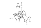
図2に示すように、マスク部材19には、集光レンズ18の焦点深度内の略中央の面に対し傾斜した姿勢で光分離面である反射透過面19aが設けられている。
Based on this signal, the
In the fluorescence confocal microscope apparatus of the present embodiment having the above configuration, the light detection unit 1 is characterized. Hereinafter, each element of the light detection unit 1 will be described in detail.
As shown in FIG. 2, the
反射透過面19aは、集光レンズ18の光軸を中心とした微小円形の透過面(ピンホール)19a’と、そのピンホール19a’の周辺領域をカバーする反射面19a”とからなる。ピンホール19a’の径raは、試料10上に形成されたスポット(集光部)の径に相当する。
このマスク部材19では、集光レンズ18から入射した光束のうち、ピンホール19a’の形成位置に入射するもの(中央光束)のみがピンホール19a’からマスク部材19の外部へ射出し、それ以外(周辺光束)は反射面19a”にて集光レンズ18の方向からずれた方向に反射する。
The reflection /
In this
マスク部材19には、さらに、その反射面19a”で反射した光束を反射する反射面19Aが、透過反射面19aと平行な姿勢で設けられている。
マスク部材19には、さらに、その反射面19Aで反射した光束に対し反射透過面19aと同じ姿勢で反射透過面19bが設けられている。
反射透過面19bは、その光束の中心近傍に配置されたピンホール19b’と、そのピンホール19b’の周辺領域をカバーする反射面19b”とからなる。ピンホール19b’の径rbは、ピンホール19a’の径raよりも大きく、例えば、rb=2raである。
The
The
The reflection /
このマスク部材19では、反射面19Aで反射した光束のうち、ピンホール19b’の形成位置に入射するもの(中央光束)のみがピンホール19b’からマスク部材19の外部へ射出し、それ以外(周辺光束)は反射面19b”にて反射面19Aからずれた方向に反射する。
マスク部材19には、さらに、その反射面19b”で反射した光束を反射する反射面19Bが、反射面19Aと同じ姿勢で設けられている。
In the
The
この反射面19Bと上述した反射面19Aとは、反射透過面19a,19bによって分離された中央光束と周辺光束とを後述する光検出器21の検出面に導光する役割を果たす。
マスク部材19には、さらに、その反射面19Bで反射した光束に対し反射透過面19bと同じ姿勢で反射透過面19cが設けられている。
The
The
反射透過面19cは、その光束の中心近傍に配置されたピンホール19c’と、そのピンホール19c’の周辺領域をカバーする反射面19c”とからなる。ピンホール19c’の径rcは、ピンホール19b’の径rbよりも大きく、例えば、rc=2rbである。
このマスク部材19では、反射面19Bで反射した光束のうち、ピンホール19c’の形成位置に入射するもの(中央光束)のみがピンホール19c’からマスク部材19の外部へ射出する。
The reflection /
In the
なお、反射透過面19aと反射面19Aとの間隔、及び反射面19Aと反射透過面19bとの間隔、及び反射透過面19bと反射面19Bとの間隔、及び反射面19Bと反射透過面19cとの間隔は、反射透過面19bと反射透過面19cとが集光レンズ18の焦点深度内に位置するよう、十分に短く設定される。
以上の構成のマスク部材19は、例えば次のようにして形成できる。
It should be noted that the distance between the reflection /
The
少なくとも、試料10からの射出光(蛍光)に対し透明な透明基板(光学ガラス基板など)を用意し、その透明基板の一方の面にその光を反射する性質の光学膜(クロム膜など)を、反射面19a”,19b”,19c”となるべき領域に成膜し、同様の性質の光学膜を、他方の面の反射面19A,19Bとなるべき領域に成膜する。
なお、反射面19a”,19b”,19c”の一部又は全部は連続していてもよい。また、反射面19A,19Bは連続していてもよい。また、この透明基板において光束が最初に入射する部分には、その入射角度を0に近づけて余分な反射光の発生を防ぐために、図2に示すような楔状の透明部材19’を貼付するとよい。透明部材19’の材料は、透明基板と同じ材料、又は透明基板と略同じ屈折率の材料であることが好ましい。また、透明基板の各箇所には、適宜、迷光の発生を防止するための反射防止膜などの公知の膜が成膜されることが好ましい。
At least prepare a transparent substrate (such as an optical glass substrate) that is transparent to the light emitted from the sample 10 (fluorescence), and an optical film (such as a chromium film) that reflects the light on one surface of the transparent substrate. Then, a film is formed in a region to be the reflection surfaces 19a ", 19b", 19c ", and an optical film having the same property is formed in a region to be the reflection surfaces 19A, 19B on the other surface.
Note that some or all of the reflecting
次に、光検出器21の検出面は、以上のマスク部材19のピンホール19a’からの射出光束の光路と、ピンホール19b’からの射出光束の光路と、ピンホール19c’からの射出光束の光路との全部をカバーできるだけのサイズを有している。
可動シャッタ20は、図2に点線で示すようにステップ状に駆動され、その駆動量に応じて少なくとも次の3つの状態Sa,Sb,Scに設定可能である。
Next, the detection surface of the
The
第1の状態Saは、ピンホール19a’からの射出光束の光路を開放し、かつピンホール19b’,19c’からの射出光束の光路を遮断する状態である。
第2の状態Sbは、ピンホール19a’,19b’からの射出光束の光路を開放し、かつピンホール19c’からの射出光束の光路を遮断する状態である。
第3の状態Scは、ピンホール19a’,19b’,19c’からの射出光束の光路を全て開放する状態である。
The first state Sa is a state in which the optical path of the emitted light beam from the
The second state Sb is a state in which the optical path of the emitted light beam from the
The third state Sc is a state in which all the optical paths of the emitted light beams from the
このような可動シャッタ20の遮光部には、様々なものが適用できる。可動シャッタ20の駆動機構に回転機構を採用した場合、例えば、図3(a),(b),(c)の何れかのように、径方向の長さが段階的に変化した羽状の部材を適用できる。
また、可動シャッタ20の駆動には、手動、電動の何れをも適用できる。因みに、電動化する場合、可動シャッタ20の駆動機構にモータ(ステッピングモータ)が取り付けられる。そのモータは、ユーザインタフェースに対し電気的に接続される。因みに、そのユーザインタフェースとして図1の入力器24を利用する場合、そのモータをコンピュータ22に対し電気的に接続すればよい。
Various things can be applied to the light shielding portion of the
Further, either manual operation or electric drive can be applied to drive the
次に、本実施形態の蛍光共焦点顕微鏡装置の効果について図4を用いて説明する。なお、図4は、マスク部材19の各反射透過面19a,19b,19cと、試料10の各層10a,10b,10cとの関係を示す模式図である。図4において、図1,図2に示すものと同じ要素については、同一符号で示した。
試料10において対物レンズ16の焦点面付近の薄い層10aから射出した光束のみがそのピンホール19a’を通過できる。
Next, the effect of the fluorescence confocal microscope apparatus of this embodiment is demonstrated using FIG. FIG. 4 is a schematic diagram showing the relationship between the reflection /
Only the light beam emitted from the
また、薄い層10aを挟む上下2層(図4の厚い層10bから薄い層10aを差し引いたもの)から射出した光束のみが、反射透過面19bのピンホール19b’を通過できる。
また、厚い層10bを挟む上下2層(図4の極めて厚い層10cから厚い層10bを差し引いたもの)から射出した光束のみが、反射透過面19cのピンホール19c’を通過できる。
Further, only the light beam emitted from the upper and lower layers sandwiching the
Further, only the light beam emitted from the upper and lower layers sandwiching the thick layer 10b (the extremely thick layer 10c in FIG. 4 minus the thick layer 10b) can pass through the pinhole 19c ′ of the reflection /
よって、可動シャッタ20が図2の第1の状態Saにあるとき(ピンホール19a’からの射出光束の光路のみが開放されているとき)には、薄い層10aが観察対象となり、その薄い層10aの画像がモニタ23上に図4の(a)のように表示される。
また、可動シャッタ20が図2の第2の状態Sbにあるとき(ピンホール19a’,19b’からの射出光束の光路のみが開放されているとき)には、厚い層10bが観察対象となり、その厚い層10bの画像がモニタ23上に図4の(b)のように表示される。
Therefore, when the
Further, when the
また、可動シャッタ20が図2の第3の状態Scにあるとき(ピンホール19a’,19b’,19cからの射出光束の光路が全て開放されているとき)には、極めて厚い層10cが観察対象となり、その極めて厚い層10cの画像がモニタ23上に図4の(c)のように表示される。
したがって、本実施形態の蛍光共焦点顕微鏡装置によれば、ユーザが可動シャッタ20を駆動するだけで、セクショニング分解能を(a),(b),(c)のとおり変更することができる。
When the
Therefore, according to the fluorescence confocal microscope apparatus of the present embodiment, the sectioning resolution can be changed as shown in (a), (b), and (c) only by driving the
ここで、この蛍光共焦点顕微鏡装置では、マスク部材19が、薄い層10aを示す光束、厚い層10bを示す光束、極めて厚い層10cを示す光束の全てを生成する。
そして、セクショニング分解能を変更する際の唯一の駆動部分である可動シャッタ20は、光束の光路を開放/遮断するだけの単純な役割しか担っていない。
よって、可動シャッタ20の位置合わせに対する要求精度は低く、その駆動機構の構成は単純化可能である。
Here, in this fluorescent confocal microscope apparatus, the
The
Therefore, the required accuracy for the alignment of the
そして、たとえ可動シャッタ20の位置合わせ精度が低くとも、マスク部材19の位置合わせさえ予め高精度に行われていれば、各層の画像はそれぞれ高精度に取得される。
したがって、本実施形態の蛍光共焦点顕微鏡装置は、シンプルな構成でありながらも高精度にセクショニング分解能を変更することができる。
(その他)
なお、本実施形態の蛍光共焦点顕微鏡装置では、光検出器に対し必要な光束を導光する手段としてマスク部材19の反射面19A,19Bを用いたが、その反射面の数を増加させたり、反射面の代わりに光ファイバ(導光方向が自在である。)を利用したりすれば、マスク部材19における反射透過面19a,19b,19cの配置自由度を高めることができる。但し、光路中の光量ロスが許容範囲内に収まるようマスク部材19は設計される必要がある。
Even if the alignment accuracy of the
Therefore, the fluorescence confocal microscope apparatus of the present embodiment can change the sectioning resolution with high accuracy while having a simple configuration.
(Other)
In the fluorescence confocal microscope apparatus of the present embodiment, the reflecting
また、可動シャッタ20の挿入角度は、図2に示すように各光束に対し略垂直にする必要はなく、各光束に対し非垂直に(例えば、マスク部材19に沿う角度に)してもよい。
また、上述した説明では、セクショニング分解能の切り換え数(マスク部材19に形成されるピンホールの数)が「3」となっているが、必要に応じて3より大きい数、又は2に増減してもよい。その増減数に応じて、反射透過面19a,19b,・・・の数を増減すればよい。
Further, the insertion angle of the
In the above description, the switching number of sectioning resolution (the number of pinholes formed in the mask member 19) is “3”. Also good. The number of reflection /
また、図1に示す光検出部1に代えて、図5に示す光検出部を適用することもできる。この検出部のマスク部材29と、図1の光検出部1のマスク部材19との間では、反射面及び透過面との利用の仕方が反転している。
以下、図5の光検出部について説明する。
この光検出部のマスク部材29には、図1に示した集光レンズ18の焦点深度内の所定面に対し傾斜した姿勢で反射透過面29aが設けられている
反射透過面29aは、集光レンズ18の光軸近傍に配置された微小円形の反射面29a’と、その反射面29a’の周辺領域をカバーする透過面29a”とからなる。反射面29a’の径raは、試料10上に形成されたスポットの径に相当する。
Moreover, it can replace with the photon detection part 1 shown in FIG. 1, and can also apply the photon detection part shown in FIG. Between the
Hereinafter, the light detection unit of FIG. 5 will be described.
The
このマスク部材29では、集光レンズ18から入射した光束のうち、反射面29a’の形成位置に入射するもの(中央光束)のみが反射面29a’にて反射してマスク部材29の外部へ射出し、それ以外(周辺光束)は透過面29a”を透過する。
マスク部材29には、さらに、その透過面29a”を透過した光束に対し反射透過面29aと同じ姿勢で反射透過面29bが設けられている。
In the
The
反射透過面29bは、その光束の中心近傍に配置された円形の反射面29b’と、反射面29b’の周辺領域をカバーする透過面29b”とからなる。反射面29b’の径rbは反射面29a’の径raよりも大きく、例えば、rb=2raである。
このマスク部材29では、透過面29a”を透過した光束のうち、反射面29b’の形成位置に入射するもの(中央光束)のみが反射面29b’にて反射してマスク部材29の外部へ射出し、それ以外(周辺光束)は透過面29b”を透過する。
The reflection /
In the
マスク部材29には、さらに、その透過面29b”を透過した光束に対し反射透過面29bと同じ姿勢で反射透過面29cが設けられている。
反射透過面29cは、その光束の中心近傍に配置された円形の反射面29c’と、反射面29c’の周辺領域をカバーする透過面29c”とからなる。反射面29c’の径rcは反射面29b’の径rbよりも大きく、例えば、rc=2rbである。
The
The reflection /
このマスク部材29では、透過面29b”を透過した光束のうち、反射面29c’の形成位置に入射するもの(中央光束)のみが反射面29c’にて反射してマスク部材29の外部へ射出する。
このマスク部材29によれば、反射透過面29a,29bによって分離された中央光束と周辺光束とが同一方向に導光される。
In the
According to the
因みに、このマスク部材29については、透明基板の必要な箇所に光を反射する性質の光学膜を成膜することによって形成できる。図5のように透明基板の内部に光学膜を成膜するためには、例えば、透明基板を2つの部材にカットし、カットしてできた2つの部材の一方の断面に光学膜を形成し、再びそれらの部材を貼り合わせればよい。
なお、反射透過面29aと反射透過面29bとの間隔、及び反射透過面29bと反射透過面29cとの間隔は、反射透過面29bと反射透過面29cとが集光レンズ18の焦点深度内に位置するよう、十分に短く設定される。
Incidentally, the
The distance between the reflection /
光検出器21の検出面は、以上のマスク部材29の反射面29a’からの射出光束の光路と、反射面29b’からの射出光束の光路と、反射面29c’からの射出光束の光路との全部をカバーできるだけのサイズを有している。
可動シャッタ20は、ステップ状に駆動され、その駆動量に応じて少なくとも次の3つの状態Sa,Sb,Scに設定可能である。
The detection surface of the
The
第1の状態Saは、反射面29a’からの射出光束の光路を開放し、かつ反射面29b’,29c’からの射出光束の光路を遮断する状態である。
第2の状態Sbは、反射面29a’,29b’からの射出光束の光路を開放し、かつ反射面29c’からの射出光束の光路を遮断する状態である。
第3の状態Scは、反射面29a’,29b’,29c’からの射出光束の光路を全て開放する状態である(以上、図5に示した光検出部の説明)。
The first state Sa is a state in which the optical path of the emitted light beam from the reflecting
The second state Sb is a state in which the optical path of the emitted light beam from the reflecting
The third state Sc is a state in which all the optical paths of the emitted light beams from the reflecting
[第2実施形態]
図6を参照して本発明の第2実施形態について説明する。ここでは、第1実施形態との相違点についてのみ説明する。
本実施形態の蛍光共焦点顕微鏡装置においては、図6に示すように、可動シャッタ20が省略され、マスク部材19のピンホール19a’,19b’,19c’と同数(ここでは3つ)の光検出器21a,21b,21cが備えられ、かつそれら光検出器21a,21b,21cと同数(ここでは3つ)のスイッチ31a,31b,31cが、光検出器21a,21b,21cとコンピュータ22との間に備えられる。このうち、マスク部材19、光検出器21a,21b,21cからなる光学系が光検出部2である。
[Second Embodiment]
A second embodiment of the present invention will be described with reference to FIG. Here, only differences from the first embodiment will be described.
In the fluorescence confocal microscope apparatus of the present embodiment, as shown in FIG. 6, the
なお、光検出器21aとスイッチ31aとの間には電流/電圧変換器(I/V)21a’が挿入され、光検出器21bとスイッチ31bとの間には電流/電圧変換器21b’が挿入され、光検出器21cとスイッチ31cとの間には電流/電圧変換器21c’が挿入される。また、スイッチ31a,31b,31cとコンピュータ22との間には、A/D変換器(A/D)21”が挿入される。また、A/D変換器21”の出力は、コンピュータ22内の画像ボード223に接続される。因みに、これら電流/電圧変換器、A/D変換器、画像ボードは、図1に示す蛍光共焦点顕微鏡装置にも同様に備えられるが、その蛍光共焦点顕微鏡装置では電流/電圧変換器の数は1である(図1では不図示。)。
A current / voltage converter (I / V) 21a ′ is inserted between the
光検出器21aの検出面は、ピンホール19a’からの射出光束の光路をカバーし、光検出器21bの検出面は、ピンホール19b’からの射出光束の光路をカバーし、光検出器21cの検出面は、ピンホール19c’からの射出光束の光路をカバーしている。
よって、光検出器21a→電流/電圧変換器21a’→スイッチ31a→A/D変換器21”の経路は、ピンホール19a’からの射出光束の光量を示す信号saの経路となる。
The detection surface of the
Therefore, the path of the
また、光検出器21b→電流/電圧変換器21b’→スイッチ31b→A/D変換器21”の経路は、ピンホール19b’からの射出光束の光量を示す信号sbの経路となる。
また、光検出器21c→電流/電圧変換器21c’→スイッチ31c→A/D変換器21”の経路は、ピンホール19c’からの射出光束の光量を示す信号scの経路となる。
それら別々の経路を経てA/D変換器21”に入力された信号sa,sb,scは、足し合わされた上で、コンピュータ22の画像ボード223に入力される。
Further, the path of the
Further, the path of the
The signals sa, sb, and sc input to the A /
画像ボード223に入力された信号は、画像ボード223上のフレームメモリMに順次書き込まれ、そのフレームメモリM上に1枚の画像を示す画像データを構築する。コンピュータ22のCPU221は、その画像データに基づいてモニタ23に画像を表示する。
ここで、コンピュータ22内のCPU221は、画像ボード223を介してスイッチ31a,31b,31cに接続されており、それらスイッチ31a,31b,31cを個別に開状態/閉状態にセットすることができる。
Signals input to the
Here, the
また、コンピュータ22に対しユーザは予め、セクショニング分解能を複数段階(ここでは、高,中,低の3段階)の何れかに指定することができる。CPU221は、インタフェース回路(I/F)224を介して入力器24からの信号を受信し、ユーザの指定した段階を認識する。
このような蛍光共焦点顕微鏡装置は、コンピュータ22内のCPU221の指示の下で次のとおり動作する。
Further, the user can designate the sectioning resolution in any one of a plurality of stages (here, three stages of high, medium, and low) for the
Such a fluorescent confocal microscope apparatus operates as follows under the instruction of the
ユーザの予め指定した段階が「高」であったとき、CPU221は、スイッチ31aを閉状態にセットし、スイッチ31b,31cを開状態にセットする。
この状態では、信号saの経路のみが開通するので、A/D変換器21”には信号saのみが入力される。よって、フレームメモリM上には、信号saによる画像データDaが構築される。したがって、モニタ23には図4(a)に示したような薄い層10aの画像が表示される。
When the stage designated in advance by the user is “high”, the
In this state, since only the path of the signal sa is opened, only the signal sa is input to the A /
ユーザの予め指定した段階が「中」であったとき、CPU221は、スイッチ31a,31bを閉状態にセットし、スイッチ31cを開状態にセットする。
この状態では、信号saの経路と信号sbの経路とが開通するので、A/D変換器21”には信号saと信号sbとのみが入力される。よって、フレームメモリM上には、信号sa,sbによる画像データDabが構築される。したがって、モニタ23には図4(b)に示したような厚い層10bの画像が表示される。
When the stage designated in advance by the user is “medium”, the
In this state, since the path of the signal sa and the path of the signal sb are opened, only the signal sa and the signal sb are input to the A /
ユーザの予め指定した段階が「低」であったとき、CPU221は、スイッチ31a,31b,31cを閉状態にセットする。
この状態では、信号saの経路と信号sbの経路と信号scの経路が全て開通するので、A/D変換器21”には信号saと信号sbと信号scとが入力される。よって、フレームメモリM上には、信号sa,sb,scによる画像データDabcが構築される。したがって、モニタ23には図4(c)に示したような極めて厚い層10cの画像が表示される。
When the stage designated in advance by the user is “low”, the
In this state, the path of the signal sa, the path of the signal sb, and the path of the signal sc are all opened, so that the signal sa, the signal sb, and the signal sc are input to the A /
したがって、本実施形態の蛍光共焦点顕微鏡装置によれば、ユーザは、入力器24を操作するだけで、セクショニング分解能を図4の(a),(b),(c)のとおり変更することができる。
ここで、この蛍光共焦点顕微鏡装置では、マスク部材19が、薄い層10aを示す光束、厚い層10bを示す光束、極めて厚い層10cを示す光束の全てを生成する。
Therefore, according to the fluorescence confocal microscope apparatus of the present embodiment, the user can change the sectioning resolution as shown in FIGS. 4A, 4B, and 4C only by operating the
Here, in this fluorescent confocal microscope apparatus, the
そして、セクショニング分解能を変更する際に駆動されるのは、コンピュータ22とスイッチ31a,31b,31cのみである。
よって、マスク部材19の位置合わせさえ予め高精度に行われていれば、各層の画像はそれぞれ高精度に取得される。
したがって、本実施形態の蛍光共焦点顕微鏡装置は、シンプルな構成でありながらも高精度にセクショニング分解能を変更することができる。
Only the
Therefore, as long as the alignment of the
Therefore, the fluorescence confocal microscope apparatus of the present embodiment can change the sectioning resolution with high accuracy while having a simple configuration.
(その他)
なお、光検出器21a,21b,21cの配置角度は、図6に示すように各光束に対し略垂直にする必要はなく、各光束に対し非垂直に(例えば、マスク部材19に沿う角度に)してもよい。
また、上記実施形態では、電気的に開閉されるスイッチ31a,31b,31c(コンピュータ22からの電気的な指示に従って開閉されるスイッチ)を説明したが、手動で開閉するスイッチ31a,31b,31cを用いることもできる。このときユーザは、入力器24を操作する代わりにそれらスイッチ31a,31b,31cを、上述したCPU221が開閉したのと同様に開閉すればよい。
(Other)
The arrangement angles of the
In the above-described embodiment, the
[第3実施形態]
図7を参照して本発明の第3実施形態について説明する。
本実施形態は、蛍光共焦点顕微鏡装置の実施形態である。ここでは、第2実施形態との相違点についてのみ説明する。
本実施形態の蛍光共焦点顕微鏡装置においては、図7に示すように、スイッチ31a,31b,31cが省略され、その代わりにコンピュータ22の内部が一部変更される。
[Third Embodiment]
A third embodiment of the present invention will be described with reference to FIG.
This embodiment is an embodiment of a fluorescence confocal microscope apparatus. Here, only differences from the second embodiment will be described.
In the fluorescence confocal microscope apparatus of this embodiment, as shown in FIG. 7, the
コンピュータ22内の画像ボード223には、光検出器21a,21b,21cから並行して出力される信号sa,sb,scを並行して格納する複数のフレームメモリMa,Mb,Mcが設けられる。また、それら信号sa,sb,scの経路には、複数のA/D変換器21a”,21b”,21c”が並列に挿入される。
また、コンピュータ22に対しユーザは予め、又は画像取得後でも、セクショニング分解能を複数段階(ここでは、高,中,低の3段階)の何れかに指定又は変更することができる。CPU221は、インタフェース回路(I/F)224を介して入力器24からの信号を受信し、ユーザの指定した段階を認識する。
The
In addition, the user can specify or change the sectioning resolution in any one of a plurality of stages (here, three stages of high, medium, and low) with respect to the
このような蛍光共焦点顕微鏡装置は、コンピュータ22内のCPU221の指示の下で次のとおり動作する。
各光検出器21a,21b,21cから並行して出力される信号sa,sb,scは、電流/電圧変換器21a’21b’,21c’,A/D変換器21a”,21b”,21c”を介してフレームメモリMa,Mb,Mcに対し並行して書き込まれる。
Such a fluorescent confocal microscope apparatus operates as follows under the instruction of the
Signals sa, sb, and sc output in parallel from the
よって、フレームメモリMa上には信号saによる画像データDaが構築され、フレームメモリMb上には信号sbによる画像データDbが構築され、フレームメモリMc上には信号scによる画像データDcが構築される。これら画像データDa,Db,Dcは、コンピュータ22内のRAM222などの記憶部に格納される。
ここで、ユーザの指定した段階が「高」であったとき、CPU221は、画像データDaをRAM222から読み出し、その画像データDaに基づく画像をモニタ23に表示する。この画像は、図4(a)に示したような薄い層10aの画像となる。
Therefore, image data Da based on the signal sa is constructed on the frame memory Ma, image data Db based on the signal sb is constructed on the frame memory Mb, and image data Dc based on the signal sc is constructed on the frame memory Mc. . These image data Da, Db, and Dc are stored in a storage unit such as the
Here, when the stage designated by the user is “high”, the
ユーザの指定した段階が「中」であったとき、CPU221は、画像データDa,DbをRAM222から読み出し、それら画像データDa,Dbの和をとり(画像データDa,Dbを重畳させ)、その和の画像データDabに基づく画像をモニタ23に表示する。この画像は、図4(b)に示したような厚い層10bの画像となる。
ユーザの指定した段階が「低」であったとき、CPU221は、画像データDa,Db,DcをRAM222から読み出し、それら画像データDa,Db,Dcの和をとり(画像データDa,Db,Dcを重畳させ)、その和の画像データDabcに基づく画像をモニタ23に表示する。この画像は、図4(c)に示したような極めて厚い層10cの画像である。
When the stage designated by the user is “medium”, the
When the stage designated by the user is “low”, the
したがって、本実施形態の蛍光共焦点顕微鏡装置によれば、ユーザは、入力器24を操作するだけで、セクショニング分解能を図4の(a),(b),(c)のとおり変更することができる。
ここで、この蛍光共焦点顕微鏡では、マスク部材19が、薄い層10aを示す光束、厚い層10bを示す光束、極めて厚い層10cを示す光束の全てを生成する。そして、セクショニング分解能を変更する際に駆動されるのは、コンピュータ22のみである。
Therefore, according to the fluorescence confocal microscope apparatus of the present embodiment, the user can change the sectioning resolution as shown in FIGS. 4A, 4B, and 4C only by operating the
Here, in this fluorescence confocal microscope, the
よって、マスク部材19の位置合わせさえ予め高精度に行われていれば、各層の画像はそれぞれ高精度に取得される。
したがって、本実施形態の蛍光共焦点顕微鏡装置は、シンプルな構成でありながらも高精度にセクショニング分解能を変更することができる。
さらに、本実施形態の蛍光共焦点顕微鏡装置は、複数の光検出器21a,21b,21cを用いて、取得した画像データを演算することで画像取得後におけるセクショニング分解能の変更や、異なる層の画像情報の取得が可能になるので、画像取得前にセクショニング分解能を指定する必要がない。そのため、画像取得のセット時間が短くなる。また、試料への光照射時間も減り、試料のダメージを軽減できる。
Therefore, as long as the alignment of the
Therefore, the fluorescence confocal microscope apparatus of the present embodiment can change the sectioning resolution with high accuracy while having a simple configuration.
Furthermore, the fluorescence confocal microscope apparatus of the present embodiment uses the plurality of
また、各画像データが並行して取得されるので、同じ時点の試料10を様々なセクショニング分解能で観察することが可能になる。
これは、時間経過に伴って状態が変化するような試料(生体試料など)を、同じ状態の下で様々なセクショニング分解能で観察したい場合などに極めて有効である。
また、各画像データは個別に記憶されるので、ユーザは所望するタイミングで所望する回数だけ、セクショニング分解能を変更することができる。
Moreover, since each image data is acquired in parallel, the
This is extremely effective when it is desired to observe a sample (such as a biological sample) whose state changes with time with various sectioning resolutions under the same state.
Further, since each image data is stored individually, the user can change the sectioning resolution as many times as desired at a desired timing.
(その他)
なお、本実施形態では、モニタ23上に同時に表示される画像が、試料10の何れかの層の画像1つのみであるかのごとく説明したが、2以上にしてよいことは言うまでもない。
[その他]
また、第2実施形態又は第3実施形態では、セクショニング分解能の切り換え数が「3」となっているが、必要に応じて3より大きい数、又は2に増減してもよい。その増減数に応じて、反射透過面19a,19b,・・・の数を増減すればよい。
(Other)
In the present embodiment, the image simultaneously displayed on the
[Others]
In the second embodiment or the third embodiment, the sectioning resolution switching number is “3”, but may be increased or decreased to a number greater than 3 or 2 as necessary. The number of reflection /
また、第2実施形態又は第3実施形態の蛍光共焦点顕微鏡装置は、図6,図7に示す光検出部2以外に、例えば図8,図9,図10,図11,図12の何れかに示すような光検出部を適用することができる。なお、適用された光検出部内の光検出器の数に応じて、上述した電流電圧変換器、スイッチ、A/D変換器、フレームメモリなどはそれぞれ最適な数だけ配置される。 Further, the fluorescence confocal microscope apparatus according to the second embodiment or the third embodiment is, for example, any one of FIG. 8, FIG. 9, FIG. 10, FIG. A light detection unit as shown in FIG. Note that the current-voltage converter, the switch, the A / D converter, the frame memory, and the like described above are arranged in an optimum number according to the number of photodetectors in the applied photodetector.
以下、図8、図9、図10、図11、図12に示す各光検出部について説明する。なお、これらの各図では図2、図5と同様、各反射透過面の符号には集光レンズ18に近い側から順に、添え字「a」,「b」,「c」,・・・を付した。また、各反射透過面において中央光束に作用する面の符号は、その反射透過面と同じ符号に「’」を付したものであり、周辺光束に作用する面の符号は、その反射透過面と同じ符号に「”」を付したものである。また、各光検出器の符号には、それに対応する反射透過面と同じ添え字「a」,「b」,「c」,・・・を付した。 Hereinafter, each of the light detection units illustrated in FIGS. 8, 9, 10, 11, and 12 will be described. In each of these drawings, as in FIGS. 2 and 5, the reference numerals of the reflection / transmission surfaces are subscripts “a”, “b”, “c”,... Was attached. In addition, the sign of the surface acting on the central light beam in each reflection / transmission surface is the same sign as that of the reflection / transmission surface, and the sign of the surface acting on the peripheral light flux is the reflection / transmission surface. The same symbol is added with “” ”. In addition, the same subscripts “a”, “b”, “c”,...
また、各図に示す何れのマスク部材においても、集光レンズ18から離れた反射透過面ほど、中央光束に作用する面(ピンホール又は反射面)の径が大きい。また、各反射透過面は何れも集光レンズ18の焦点深度内に配置されている。
図8に示す光検出部のマスク部材29は、図5に示したのと同じマスク部材である。つまり、反射透過面29a,29b,29cの中央が反射面29a’,29b’,29c’、その周辺が透過面29a”,29b”,29c”となっている。光検出器21a,21b,21cは、それら反射面29a’,29b’,29c’からの射出光束の光路を個別にカバーする。
In any of the mask members shown in the drawings, the diameter of the surface (pinhole or reflection surface) that acts on the central light beam is larger as the reflection / transmission surface is farther from the
The
図9に示す光検出部のマスク部材39は、図2に示したマスク部材29において、反射面19Aの位置に反射透過面19b、反射透過面19bの位置に反射透過面19cを設けたものである。
図10に示す光検出部のマスク部材29は、図8に示したのと同じマスク部材である。但し、この光検出部には光検出器21dが追加されている。光検出器21dは、反射透過面29cの透過面29c”を透過した光束の光路をカバーする。
The
The
図11に示す光検出部のマスク部材59は、マスク部材29において、集光レンズ18に近い方から数えて2番目の反射透過面29bの傾斜方向が、他の反射透過面29a,29cの傾斜方向と反対になったものである。光検出器21bは、そのような反射透過面29bの反射面29b’からの射出光束の光路をカバーする。
図12に示す光検出部のマスク部材69には、透明基板を用いた他のマスク部材とは異なり、プリズム(ここでは5角プリズム)が用いられている。
In the
Unlike the other mask members using a transparent substrate, a prism (here, a pentagonal prism) is used for the
マスク部材69は、5角プリズムの第2面、第3面に、ピンホール69a’と反射面69a”とからなる反射透過面69a、ピンホール69b’と反射面69b”とからなる反射透過面69aをそれぞれ設けてなる。
光検出器21aは、ピンホール69a’からの射出光束の光路をカバーし、光検出器21bは、ピンホール69b’からの射出光束の光路をカバーし、光検出器21cは、マスク部材69において何ら反射透過面を設けていない最終面(第5面)からの射出光束の光路をカバーする。
The
The
因みに、その光検出器21cの前側には、マスク部材69の各ピンホール69a’,69b’よりも大きい開口69c’を有した絞り69cが配置されている。
他の光検出部内の同様の光検出器(図9の光検出器21d,図10の光検出器21d、図11の光検出器21d)の全段にも、同様の絞りを配置してもよい。
また、上記各実施形態は、蛍光共焦点顕微鏡装置(蛍光観察用の共焦点顕微鏡装置)の実施形態であるが、本発明は、蛍光観察用以外の共焦点顕微鏡装置にも同様に適用可能である。
Incidentally, a
Similar apertures may be arranged in all stages of similar photodetectors (the
Each of the above embodiments is an embodiment of a fluorescent confocal microscope apparatus (a confocal microscope apparatus for fluorescence observation), but the present invention can be similarly applied to a confocal microscope apparatus other than for fluorescence observation. is there.
11 光源
12 照明用レンズ
13,17 フィルタ
14 ダイクロイックミラー
15 ガルバノミラー
16 対物レンズ
18 集光レンズ
19,29,39,59,69 マスク部材
19a,19b,・・・,29a,29b,・・・,69a,69b,・・・ 反射透過面
19a”,19b”,・・・,29a’,29b’,・・・,69a”,69b”,・・・反射面
19a’,19b’,・・・,69a’,69b’,・・・ピンホール
29a”,29b”,・・・透過面
69c 絞り
69c’ 開口
20 可動シャッタ
21 光検出器
22 コンピュータ
23 モニタ
24 入力器
21’電流/電圧変換器(I/V)
31 スイッチ
21”A/D変換器(A/D)
M フレームメモリ
221 CPU
222 RAM
224 インタフェース回路(I/F)
DESCRIPTION OF
31
222 RAM
224 interface circuit (I / F)
Claims (7)
前記光源からの光を試料に集光する照明光学系と、
前記試料からの光を結像する結像光学系と、
前記結像光学系に関し前記試料の集光点と略共役な位置に入射する光を、少なくとも前記試料の前記集光点の近傍領域からの光と、その周辺領域からの光とに分離し、それぞれ検出する検出手段とを備え、
前記検出手段は、
前記結像光学系の焦点深度内に光軸に対して傾斜して配置された光学部材と、前記光学部材において前記集光点と略共役な位置に設けられ、かつその位置に入射する光を前記近傍領域からの光と前記周辺領域からの光とに分離する光分離面と、前記近傍領域からの光と前記周辺領域からの光とを独立して検出する検出器とを有し、
前記光分離面は、
前記近傍領域からの光を受ける円形の第1面と、前記周辺領域からの光を受ける第2面とを有し、
前記光学部材は、
前記周辺領域からの光の光路に対し直列の関係で複数の前記光分離面を配置しており、
前記複数の光分離面の間では、
後段に配置されたものほど前記第1面の径が大きく設定され、
前記複数の光分離面の間では、
前記第1面のタイプは透過面及び反射面の一方に統一され、かつ前記第2面のタイプは透過面及び反射面の他方に統一されている
ことを特徴とする共焦点顕微鏡。 A light source;
An illumination optical system for condensing the light from the light source onto the sample;
An imaging optical system for imaging light from the sample;
Separating light incident on a position substantially conjugate with the focal point of the sample with respect to the imaging optical system into at least light from a region near the focal point of the sample and light from its peripheral region; Detecting means for detecting each ,
The detection means includes
An optical member disposed at an inclination with respect to the optical axis within the focal depth of the imaging optical system, and light that is provided at a position that is substantially conjugate with the condensing point in the optical member and that enters the position. A light separation surface that separates light from the neighboring region and light from the peripheral region, and a detector that independently detects light from the neighboring region and light from the peripheral region,
The light separation surface is
A circular first surface that receives light from the neighboring region and a second surface that receives light from the peripheral region;
The optical member is
A plurality of the light separation surfaces are arranged in series with respect to the optical path of light from the peripheral region,
Among the plurality of light separation surfaces,
The diameter of the first surface is set to be larger in the latter stage,
Among the plurality of light separation surfaces,
The confocal microscope characterized in that the first surface type is unified with one of a transmissive surface and a reflective surface, and the second surface type is unified with the other of the transmissive surface and the reflective surface .
複数の前記検出器を備える
ことを特徴とする請求項1に記載の共焦点顕微鏡。 The detection means includes
The confocal microscope according to claim 1 , comprising a plurality of the detectors .
前記近傍領域からの光を検出する第1の前記検出器と、前記周辺領域からの光を検出する第2の前記検出器とを有する A first detector for detecting light from the neighboring region; and a second detector for detecting light from the peripheral region.
ことを特徴とする請求項2に記載の共焦点顕微鏡。 The confocal microscope according to claim 2.
前記分離された前記近傍領域からの光と前記周辺領域からの光との双方を受光する単一の検出器と、
前記近傍領域からの光の光路と、前記周辺領域からの光の光路との一方を開閉するシャッターとを有し、
前記光学部材は、前記近傍領域からの光及び前記周辺領域からの光を前記単一の検出器へ導く
ことを特徴とする請求項1に記載の共焦点顕微鏡。 The detection means includes
A single detector that receives both the separated light from the neighboring region and the light from the peripheral region;
And a shutter for opening and closing the optical path of the light from the neighboring region, one of the optical path of the light from the peripheral region,
The confocal microscope according to claim 1 , wherein the optical member guides light from the vicinity region and light from the peripheral region to the single detector .
前記近傍領域からの光と前記周辺領域からの光との光量和、又は、前記近傍領域からの光の光量を検出する
ことを特徴とする請求項4に記載の共焦点顕微鏡。 The detection means includes
The confocal microscope according to claim 4 , wherein a light amount sum of light from the neighboring region and light from the peripheral region or a light amount of light from the neighboring region is detected.
前記複数の検出器が生成する複数の検出信号のうち少なくとも2つを選択し、加算する選択加算手段と
を備えることを特徴とする共焦点顕微鏡システム。 A confocal microscope according to claim 2 ;
A confocal microscope system comprising: a selection addition unit that selects and adds at least two of the plurality of detection signals generated by the plurality of detectors.
前記複数の検出器が生成する複数の検出信号を個別に記憶する記憶手段と、
前記記憶手段が記憶した複数の検出信号を用いて演算する演算処理手段と
を備えることを特徴とする共焦点顕微鏡システム。 A confocal microscope according to claim 2 ;
Storage means for individually storing a plurality of detection signals generated by the plurality of detectors;
A confocal microscope system comprising: an arithmetic processing unit configured to perform calculation using a plurality of detection signals stored in the storage unit.
Priority Applications (4)
| Application Number | Priority Date | Filing Date | Title |
|---|---|---|---|
| JP2004083319A JP4677728B2 (en) | 2004-03-22 | 2004-03-22 | Confocal microscope and confocal microscope system |
| US11/081,731 US7271953B2 (en) | 2004-03-22 | 2005-03-17 | Confocal microscope |
| GB0505755A GB2412528B (en) | 2004-03-22 | 2005-03-21 | Confocal microscope |
| DE102005012993A DE102005012993A1 (en) | 2004-03-22 | 2005-03-21 | Confocal microscope |
Applications Claiming Priority (1)
| Application Number | Priority Date | Filing Date | Title |
|---|---|---|---|
| JP2004083319A JP4677728B2 (en) | 2004-03-22 | 2004-03-22 | Confocal microscope and confocal microscope system |
Publications (3)
| Publication Number | Publication Date |
|---|---|
| JP2005274591A JP2005274591A (en) | 2005-10-06 |
| JP2005274591A5 JP2005274591A5 (en) | 2007-06-14 |
| JP4677728B2 true JP4677728B2 (en) | 2011-04-27 |
Family
ID=34545165
Family Applications (1)
| Application Number | Title | Priority Date | Filing Date |
|---|---|---|---|
| JP2004083319A Expired - Fee Related JP4677728B2 (en) | 2004-03-22 | 2004-03-22 | Confocal microscope and confocal microscope system |
Country Status (4)
| Country | Link |
|---|---|
| US (1) | US7271953B2 (en) |
| JP (1) | JP4677728B2 (en) |
| DE (1) | DE102005012993A1 (en) |
| GB (1) | GB2412528B (en) |
Families Citing this family (14)
| Publication number | Priority date | Publication date | Assignee | Title |
|---|---|---|---|---|
| GB0221014D0 (en) * | 2002-09-11 | 2002-10-23 | Medical Res Council | Spectral discrimination apparatus and method |
| WO2006128442A1 (en) * | 2005-05-31 | 2006-12-07 | W.O.M. World Of Medicine Ag | Method and apparatus for visual characterization of tissue |
| JP2007279085A (en) * | 2006-04-03 | 2007-10-25 | Nikon Corp | Confocal microscope |
| DE602008006373D1 (en) * | 2007-02-26 | 2011-06-01 | Koninkl Philips Electronics Nv | METHOD AND DEVICE FOR OPTICAL TISSUE ANALYSIS |
| JP4735758B2 (en) | 2007-06-13 | 2011-07-27 | 株式会社ニコン | Confocal microscope |
| WO2008155883A1 (en) * | 2007-06-15 | 2008-12-24 | Nikon Corporation | Confocal microscope device |
| DE102010006662B4 (en) * | 2010-02-03 | 2019-07-25 | Diehl Defence Gmbh & Co. Kg | Apparatus and method for mapping an environment to a detector device |
| DE112015001154T5 (en) | 2014-04-24 | 2016-12-08 | Olympus Corporation | Microscope and microscopy method |
| CN104296687A (en) * | 2014-11-05 | 2015-01-21 | 哈尔滨工业大学 | Smooth large-curvature sample measurement device and method based on fluorescent confocal microscopy |
| CN104568884B (en) * | 2014-12-31 | 2017-03-29 | 深圳先进技术研究院 | Fluorescence microscopy system and method based on focal spot modulation |
| WO2017046863A1 (en) | 2015-09-15 | 2017-03-23 | オリンパス株式会社 | Microscope and microscope observation method |
| US11042016B2 (en) * | 2017-12-12 | 2021-06-22 | Trustees Of Boston University | Multi-Z confocal imaging system |
| CN108759698B (en) * | 2018-08-02 | 2020-02-14 | 淮阴师范学院 | Low-coherence light interference measuring method and device for mirror surface spacing of multi-mirror lens group |
| WO2023224929A1 (en) * | 2022-05-16 | 2023-11-23 | Colgate-Palmolive Company | Technologies for simultaneous sampling of more than one sample plane using a mirrored pinhole array |
Citations (4)
| Publication number | Priority date | Publication date | Assignee | Title |
|---|---|---|---|---|
| JPH02221909A (en) * | 1989-02-22 | 1990-09-04 | Hamamatsu Photonics Kk | Confocal scanning microscope |
| JPH08136815A (en) * | 1994-11-11 | 1996-05-31 | Olympus Optical Co Ltd | Confocal scan type optical microscope |
| JPH11237557A (en) * | 1998-02-23 | 1999-08-31 | Olympus Optical Co Ltd | Scanning type optical microscope |
| JP2001511902A (en) * | 1996-12-05 | 2001-08-14 | ライカ ミクロジュステムス ハイデルベルク ゲーエムベーハー | Apparatus and method for simultaneous multifocal imaging of surface profiles of arbitrary objects |
Family Cites Families (8)
| Publication number | Priority date | Publication date | Assignee | Title |
|---|---|---|---|---|
| JPH0616927A (en) | 1992-06-30 | 1994-01-25 | Kanebo Ltd | Polyamide resin composition |
| DE4330347C2 (en) | 1993-09-08 | 1998-04-09 | Leica Lasertechnik | Use of a device for the selection and detection of at least two spectral ranges of a light beam |
| US5886784A (en) | 1993-09-08 | 1999-03-23 | Leica Lasertechink Gmbh | Device for the selection and detection of at least two spectral regions in a beam of light |
| US5932871A (en) | 1995-11-08 | 1999-08-03 | Olympus Optical Co., Ltd. | Microscope having a confocal point and a non-confocal point, and a confocal point detect method applied thereto |
| JP3816632B2 (en) * | 1997-05-14 | 2006-08-30 | オリンパス株式会社 | Scanning microscope |
| GB9825267D0 (en) | 1998-11-19 | 1999-01-13 | Medical Res Council | Scanning confocal optical microscope system |
| US6423960B1 (en) * | 1999-12-31 | 2002-07-23 | Leica Microsystems Heidelberg Gmbh | Method and system for processing scan-data from a confocal microscope |
| DE10132638A1 (en) * | 2001-07-05 | 2003-01-16 | Leica Microsystems | Scanning microscope and method for wavelength-dependent detection |
-
2004
- 2004-03-22 JP JP2004083319A patent/JP4677728B2/en not_active Expired - Fee Related
-
2005
- 2005-03-17 US US11/081,731 patent/US7271953B2/en not_active Expired - Fee Related
- 2005-03-21 DE DE102005012993A patent/DE102005012993A1/en not_active Withdrawn
- 2005-03-21 GB GB0505755A patent/GB2412528B/en not_active Expired - Fee Related
Patent Citations (4)
| Publication number | Priority date | Publication date | Assignee | Title |
|---|---|---|---|---|
| JPH02221909A (en) * | 1989-02-22 | 1990-09-04 | Hamamatsu Photonics Kk | Confocal scanning microscope |
| JPH08136815A (en) * | 1994-11-11 | 1996-05-31 | Olympus Optical Co Ltd | Confocal scan type optical microscope |
| JP2001511902A (en) * | 1996-12-05 | 2001-08-14 | ライカ ミクロジュステムス ハイデルベルク ゲーエムベーハー | Apparatus and method for simultaneous multifocal imaging of surface profiles of arbitrary objects |
| JPH11237557A (en) * | 1998-02-23 | 1999-08-31 | Olympus Optical Co Ltd | Scanning type optical microscope |
Also Published As
| Publication number | Publication date |
|---|---|
| GB2412528A (en) | 2005-09-28 |
| DE102005012993A1 (en) | 2005-10-13 |
| US7271953B2 (en) | 2007-09-18 |
| US20050213206A1 (en) | 2005-09-29 |
| GB2412528B (en) | 2009-10-21 |
| GB0505755D0 (en) | 2005-04-27 |
| JP2005274591A (en) | 2005-10-06 |
Similar Documents
| Publication | Publication Date | Title |
|---|---|---|
| US7271953B2 (en) | Confocal microscope | |
| EP1857853B1 (en) | Illuminating device | |
| US7369308B2 (en) | Total internal reflection fluorescence microscope | |
| JP4315794B2 (en) | Confocal microscope | |
| JP5712342B2 (en) | Optical microscope and spectrum measuring method | |
| JP2019117387A (en) | High-resolution scanning microscopic method | |
| EP2053442A1 (en) | Scanning laser microscope | |
| JP2012212155A (en) | Method and apparatus for fluorescent confocal microscopy | |
| US20100172021A1 (en) | Laser microscope | |
| EP1906224B1 (en) | Confocal Microscope Apparatus | |
| JP4854880B2 (en) | Laser microscope | |
| US6496307B2 (en) | Confocal scanning microscope | |
| JP5495740B2 (en) | Confocal scanning microscope | |
| JP4128387B2 (en) | Microscope equipment | |
| JP2002214533A (en) | Confocal microscope | |
| JP4725967B2 (en) | Minute height measuring device and displacement meter unit | |
| US6903816B2 (en) | Mirror driving mechanism, and spectroscope and scanning laser microscope comprising mirror which is driven by mirror driving mechanism | |
| JP5825476B2 (en) | Microscope equipment | |
| JP2002023059A (en) | Microscope assembly | |
| JP2011118265A (en) | Microscope device | |
| JP3486754B2 (en) | Scanning optical microscope | |
| JP3917705B2 (en) | Scanning optical microscope | |
| JP5307868B2 (en) | Total reflection microscope | |
| JPH0593845A (en) | Automatic focus detecting device | |
| JP3115100U (en) | microscope |
Legal Events
| Date | Code | Title | Description |
|---|---|---|---|
| A621 | Written request for application examination |
Free format text: JAPANESE INTERMEDIATE CODE: A621 Effective date: 20070309 |
|
| A521 | Request for written amendment filed |
Free format text: JAPANESE INTERMEDIATE CODE: A523 Effective date: 20070419 |
|
| A977 | Report on retrieval |
Free format text: JAPANESE INTERMEDIATE CODE: A971007 Effective date: 20100413 |
|
| A131 | Notification of reasons for refusal |
Free format text: JAPANESE INTERMEDIATE CODE: A131 Effective date: 20100427 |
|
| A521 | Request for written amendment filed |
Free format text: JAPANESE INTERMEDIATE CODE: A523 Effective date: 20100623 |
|
| TRDD | Decision of grant or rejection written | ||
| A01 | Written decision to grant a patent or to grant a registration (utility model) |
Free format text: JAPANESE INTERMEDIATE CODE: A01 Effective date: 20110104 |
|
| A01 | Written decision to grant a patent or to grant a registration (utility model) |
Free format text: JAPANESE INTERMEDIATE CODE: A01 |
|
| A61 | First payment of annual fees (during grant procedure) |
Free format text: JAPANESE INTERMEDIATE CODE: A61 Effective date: 20110117 |
|
| R150 | Certificate of patent or registration of utility model |
Ref document number: 4677728 Country of ref document: JP Free format text: JAPANESE INTERMEDIATE CODE: R150 Free format text: JAPANESE INTERMEDIATE CODE: R150 |
|
| FPAY | Renewal fee payment (event date is renewal date of database) |
Free format text: PAYMENT UNTIL: 20140210 Year of fee payment: 3 |
|
| FPAY | Renewal fee payment (event date is renewal date of database) |
Free format text: PAYMENT UNTIL: 20140210 Year of fee payment: 3 |
|
| R250 | Receipt of annual fees |
Free format text: JAPANESE INTERMEDIATE CODE: R250 |
|
| R250 | Receipt of annual fees |
Free format text: JAPANESE INTERMEDIATE CODE: R250 |
|
| R250 | Receipt of annual fees |
Free format text: JAPANESE INTERMEDIATE CODE: R250 |
|
| R250 | Receipt of annual fees |
Free format text: JAPANESE INTERMEDIATE CODE: R250 |
|
| R250 | Receipt of annual fees |
Free format text: JAPANESE INTERMEDIATE CODE: R250 |
|
| R250 | Receipt of annual fees |
Free format text: JAPANESE INTERMEDIATE CODE: R250 |
|
| R250 | Receipt of annual fees |
Free format text: JAPANESE INTERMEDIATE CODE: R250 |
|
| R250 | Receipt of annual fees |
Free format text: JAPANESE INTERMEDIATE CODE: R250 |
|
| R250 | Receipt of annual fees |
Free format text: JAPANESE INTERMEDIATE CODE: R250 |
|
| LAPS | Cancellation because of no payment of annual fees |