JP4671473B2 - Mask data correction apparatus, method for manufacturing transfer mask, and method for manufacturing apparatus having pattern structure - Google Patents
Mask data correction apparatus, method for manufacturing transfer mask, and method for manufacturing apparatus having pattern structure Download PDFInfo
- Publication number
- JP4671473B2 JP4671473B2 JP2000214002A JP2000214002A JP4671473B2 JP 4671473 B2 JP4671473 B2 JP 4671473B2 JP 2000214002 A JP2000214002 A JP 2000214002A JP 2000214002 A JP2000214002 A JP 2000214002A JP 4671473 B2 JP4671473 B2 JP 4671473B2
- Authority
- JP
- Japan
- Prior art keywords
- image
- unit
- mesh
- mask
- mask data
- Prior art date
- Legal status (The legal status is an assumption and is not a legal conclusion. Google has not performed a legal analysis and makes no representation as to the accuracy of the status listed.)
- Expired - Fee Related
Links
Images


Classifications
-
- H—ELECTRICITY
- H01—ELECTRIC ELEMENTS
- H01L—SEMICONDUCTOR DEVICES NOT COVERED BY CLASS H10
- H01L22/00—Testing or measuring during manufacture or treatment; Reliability measurements, i.e. testing of parts without further processing to modify the parts as such; Structural arrangements therefor
-
- G—PHYSICS
- G03—PHOTOGRAPHY; CINEMATOGRAPHY; ANALOGOUS TECHNIQUES USING WAVES OTHER THAN OPTICAL WAVES; ELECTROGRAPHY; HOLOGRAPHY
- G03F—PHOTOMECHANICAL PRODUCTION OF TEXTURED OR PATTERNED SURFACES, e.g. FOR PRINTING, FOR PROCESSING OF SEMICONDUCTOR DEVICES; MATERIALS THEREFOR; ORIGINALS THEREFOR; APPARATUS SPECIALLY ADAPTED THEREFOR
- G03F7/00—Photomechanical, e.g. photolithographic, production of textured or patterned surfaces, e.g. printing surfaces; Materials therefor, e.g. comprising photoresists; Apparatus specially adapted therefor
- G03F7/70—Microphotolithographic exposure; Apparatus therefor
- G03F7/70425—Imaging strategies, e.g. for increasing throughput or resolution, printing product fields larger than the image field or compensating lithography- or non-lithography errors, e.g. proximity correction, mix-and-match, stitching or double patterning
- G03F7/70433—Layout for increasing efficiency or for compensating imaging errors, e.g. layout of exposure fields for reducing focus errors; Use of mask features for increasing efficiency or for compensating imaging errors
-
- G—PHYSICS
- G03—PHOTOGRAPHY; CINEMATOGRAPHY; ANALOGOUS TECHNIQUES USING WAVES OTHER THAN OPTICAL WAVES; ELECTROGRAPHY; HOLOGRAPHY
- G03F—PHOTOMECHANICAL PRODUCTION OF TEXTURED OR PATTERNED SURFACES, e.g. FOR PRINTING, FOR PROCESSING OF SEMICONDUCTOR DEVICES; MATERIALS THEREFOR; ORIGINALS THEREFOR; APPARATUS SPECIALLY ADAPTED THEREFOR
- G03F1/00—Originals for photomechanical production of textured or patterned surfaces, e.g., masks, photo-masks, reticles; Mask blanks or pellicles therefor; Containers specially adapted therefor; Preparation thereof
- G03F1/68—Preparation processes not covered by groups G03F1/20 - G03F1/50
-
- H—ELECTRICITY
- H01—ELECTRIC ELEMENTS
- H01J—ELECTRIC DISCHARGE TUBES OR DISCHARGE LAMPS
- H01J37/00—Discharge tubes with provision for introducing objects or material to be exposed to the discharge, e.g. for the purpose of examination or processing thereof
- H01J37/30—Electron-beam or ion-beam tubes for localised treatment of objects
- H01J37/302—Controlling tubes by external information, e.g. programme control
- H01J37/3023—Programme control
-
- H—ELECTRICITY
- H01—ELECTRIC ELEMENTS
- H01J—ELECTRIC DISCHARGE TUBES OR DISCHARGE LAMPS
- H01J2237/00—Discharge tubes exposing object to beam, e.g. for analysis treatment, etching, imaging
- H01J2237/30—Electron or ion beam tubes for processing objects
- H01J2237/317—Processing objects on a microscale
- H01J2237/3175—Lithography
- H01J2237/31793—Problems associated with lithography
- H01J2237/31794—Problems associated with lithography affecting masks
Landscapes
- Physics & Mathematics (AREA)
- General Physics & Mathematics (AREA)
- Chemical & Material Sciences (AREA)
- Analytical Chemistry (AREA)
- Engineering & Computer Science (AREA)
- Manufacturing & Machinery (AREA)
- Computer Hardware Design (AREA)
- Microelectronics & Electronic Packaging (AREA)
- Power Engineering (AREA)
- Preparing Plates And Mask In Photomechanical Process (AREA)
- Exposure And Positioning Against Photoresist Photosensitive Materials (AREA)
- Exposure Of Semiconductors, Excluding Electron Or Ion Beam Exposure (AREA)
Description
【0001】
【発明の属する技術分野】
この発明は、マスクデータ補正装置、フーリエ変換装置、アップサンプリング装置、ダウンサンプリング装置、転写用マスクの製造方法、および、パターン構造を有する装置の製造方法に関し、特に、精度を保ちつつ能率を向上させるための改良に関する。
【0002】
【従来の技術】
近年において、大規模集積回路(LSI)の微細化の進展にはめざましいものがあるが、これを可能にしたのが微細加工技術の発展である。その中でも光転写技術は、一括露光による高いスループット、100年来連綿と培ってきた光学技術の実績などにより、現在もなお、微細加工技術の中心に位置している。
【0003】
しかしながら、微細パターンの加工寸法が、露光光の波長よりも小さくなってしまった現在では、光転写技術の限界を見極めること、解像力および焦点深度の限界を克服することなどが重要となっている。このような解析を行うために、光学像計算を行う技術、計算した光学像から発生したひずみを補正する技術などは、近年特に注目を浴びている。図32は、その一例として、特開平8−297692号公報(以下、文献1)に開示される本願発明者の発明になるマスクデータ補正方法の手順を示すフローチャートである。
【0004】
この方法は、文献1に詳細に開示されており、既に周知技術であるので、ここでは簡単に紹介するにとどめる。この方法による処理S90が開始されると、回路設計およびレイアウト設計が行われることにより(S91,S92)、まず、レイアウトデータが記憶媒体に格納される(S93)。このレイアウトデータは、階層構造を有する図形の基本要素の形状と階層構造とを規定する。つぎに、レイアウトデータが展開され(S94)、プロセス条件が入力される(S95)。その後、メッシュが生成され(S96)、画像計算が行われる(S97)。つぎに、画像計算の結果とレイアウトデータとの比較を通じて、図形の補正が行われ(S98)、その結果である補正データが出力される(S99)ことにより、処理S90が終了する。
【0005】
さらに、これらの技術の使用にあたっては、光学系の収差に起因する光学像の劣化などにも注意を払う必要がある。この技術に関しては、いずれも本願発明者の発明になる特開平9−167731号公報(以下、文献2)あるいは特開平10−335224号公報(以下、文献3)に、その詳細が述べられている。さらに、フルショットレベルの長距離相関が問題となるケースもある。
【0006】
これらの評価あるいは最適化を行うためには、様々なケースに関して、光学像に関する計算結果と実験結果との対応関係を調べる必要がある。しかしながら、光学像に関する計算は、マスク図形をフーリエ変換した後、逆フーリエ変換する必要があるなど、一般的に多大な計算量を必要とする。そのため、フーリエ変換を高速に実行するために、多くの提案がなされている。一般的なものとしては:
(1) 高速フーリエ変換(FFT;Fast Fourier Transformation)(例えば、「科学計測のための波形データ処理」南茂夫,CQ出版社,に記載);
(2) OCA(Optical Coherent Approximation)(例えば、Y.C Pali and T.Kailath J.OP Soc.Am A,Vol.11(1994)2438に記載);
(3) 不等間隔フーリエ変換(例えば、E.Barouch,B.Bradie,U.Hollerbach,and S.A.Orszag,J.Vac.Sci.and Technol.B8(1990)1432;E.Barouch,B.Bradie, U.Hollerbach,and S.A.Orszag,Proc.SPIE Vol.1465(1991)254;E.Barouch,U.Hollerbach,S.A.Orszag,B.Bradie and M.Peckcrar,IEEE Electron Device Lett.,EDL-12(1991)513などに記載);
(4) 部分コピーレント近似(例えば、M.Yeung:Proc,Kodak Microelectoronics Seminar INTERFACE '85(KTI Chemicals,Inc,San Diego,1986)p.115;M.Yeung:Proc.SPIE Vol.922(1988)149などに記載);および、
(5) 超並列演算(例えば、K,Kamon, W.Wakamiya,H.Nagata a,K.Moriizumi,T,Miyamoto ,Y ,Myoi and M.Tanaka;Proc,SPIE Vol.2512(1995)491;T.Hanawa,K.kamon,A.Nakae,S.Nakao,and K.Moriizumi: Proc,SPIE Vol.2726(1996)640;A.Nakae,K.Kamon,T.Hanawa,K.Moriizumi and S.Nakao :Jpn.J.Appl.phys.Vol.35(1996)6395などに記載)が、知られている。
【0007】
これらの技術を通じて、近年には、著しい高速度化が進められてきた。これらの技術は、それぞれに非常に有効な技術であり、微細加工技術の革新に多大な貢献をなしたが、LSIのフルショット計算をするには、これらを組み合わせてもまだ十分とは云えない。なぜなら、一例として現在開発中である1G(ギガ)ビットのDRAMを挙げると、1G個という膨大な数のトランジスタを縦横に敷き詰めることにより、メモリセルアレイが形成されるからである。また、ロジックデバイス(論理回路)であっても、小規模なRAMが数多く含まれた構造を有している。さらに加えて、LSIは今後ともますます高集積化が進むものと考えられている。
【0008】
従来は、一旦フラット展開を行った後で図形データを処理する手法(例えば、cadence社のdracula)が一般的であった。これに対して、大量の図形を扱うために、図形データの階層構造を利用してレイアウト検証等の演算を実行する装置(例えば、arant社のhercules;menter社のcaliber;lucent社のcloverなど)が、最近において開発されている。これらの装置では、図33が例示するように、いくつかのデータをセル91にまとめると共に、セル同士の配置や階層構造を維持したまま、図形演算等処理することによって高速化が図られていた。図33では、画像生成領域90に多数のセル91が配置され、セル91の中に図形の基本要素92が配置されている。
【0009】
これらの装置は、図形同士の単純な演算、比較などを速く実行できるので、デザインルールチェック、簡単な図形同士の論理演算、あるいはサイジング等の用途に適している。
【0010】
【発明が解決しようとする課題】
しかしながら、ある図形の影響あるいは相関が、複数のセルにまたがって広く及ぶ場合では、各要素セルを展開せざるを得ないので、データ処理の高速化を達成できないばかりでなく、むしろ、処理能力が劣化する場合すらあることが知られている。
【0011】
一方、光学像計算の用途では、ある図形の影響は、光学系の可干渉距離内に及んでいる。また、ドライエッチングにおけるマイクロローディング効果あるいはマスク描画における近接効果は、約10μmにも及ぶ場合がある、従って、図形要素同士が互いに干渉や影響し合う様子を計算する必要がある。むしろ、リソグラフィをはじめとする各種のプロセスシミュレーションでは、この相関の様子を計算することこそが本質であると言える。そして、この光学的な干渉性あるいは各種近接効果は、一般に複数のセルにまたがっている場合が多いので、従来においてはセルを全展開して評価する必要があった。従って、階層化されたデータを近接補正計算に利用しても、最終的にはやはり全展開せざるを得ず、階層処理の有効性を十分に発揮できないという問題点があった。
【0012】
本発明は、従来の技術における上記した問題点を解消するためになされたもので、レイアウトデータの階層構造を有効に利用して、精度を高く維持しつつ処理の能率を高めることのできるマスクデータ補正装置、転写用マスクの製造方法、および、パターン構造を有する装置の製造方法を提供することを目的とする。
【0013】
【課題を解決するための手段】
第1の発明の装置は、階層構造を有する図形の基本要素の形状と前記階層構造とを規定するレイアウトデータと、製造プロセス条件とにもとづいて、製造プロセスに用いられる転写用マスクのパターン形状を表現するマスクデータを、製造プロセスで予測されるひずみを抑制する形態で生成するマスクデータ補正装置であって、前記基本要素をフーリエ変換することにより前記基本要素のフーリエ像を得るフーリエ変換部と、前記階層構造にもとづいて前記基本要素の前記フーリエ像をフーリエ空間内で合成することにより前記図形のフーリエ像を得る合成部と、前記図形の前記フーリエ像に対して、前記ひずみに対応した空間フィルタ処理を施す空間フィルタ部と、前記空間フィルタ処理を施された前記フーリエ像に対して、逆フーリエ変換を行うことにより、前記ひずみを反映した逆フーリエ像を得る逆フーリエ変換部と、前記図形変換部が出力する前記図形と前記レイアウトデータが規定する前記図形とを比較することにより、前記ひずみを抑制する方向へ、前記レイアウトデータが規定する前記図形を補正し、前記マスクデータとして出力する図形補正部と、を備える。
【0014】
第2の発明の装置では、第1の発明のマスクデータ補正装置において、前記ひずみが、前記マスクデータにもとづいて電子線描画を用いて前記転写用マスクを形成する際に生じる描画ひずみを含む。
【0015】
第3の発明の装置では、第1または第2の発明のマスクデータ補正装置において、前記ひずみが、前記マスクデータにもとづいて形成された前記転写用マスクを用いて転写を実行するときに転写像に生じる転写ひずみを含む。
【0016】
第4の発明の装置では、第1ないし第3のいずれかの発明のマスクデータ補正装置において、前記ひずみが、前記マスクデータにもとづいて形成された前記転写用マスクを転写することにより形成されたレジストパターンを用いて選択的エッチングを実行するときに、エッチングパターンに生じるエッチングひずみを含む。
【0017】
第5の発明の装置では、第1ないし第4のいずれかの発明のマスクデータ補正装置において、前記ひずみが、前記マスクデータにもとづいて形成された前記転写用マスクを転写することにより形成されたレジストパターンを用いて選択的エッチングを実行した後に、堆積された膜に対する研磨処理を実行するときに研磨後のパターンに生じる研磨ひずみを含む。
【0018】
第6の発明の装置では、第1ないし第4のいずれかの発明のマスクデータ補正装置において、前記ひずみが、前記マスクデータにもとづいて形成された前記転写用マスクを転写することにより形成されたレジストパターンを用いて選択的エッチングを実行した後に、堆積された膜に対するエッチバック処理を実行するときにエッチバック後のパターンに生じるエッチバックひずみを含む。
【0019】
第7の発明の装置では、第1ないし第6のいずれかの発明のマスクデータ補正装置において、前記フーリエ変換部が、前記基本要素を、三角形と四角形と円形とのいずれかである要素図形の群へと分割する図形分割部と、前記要素図形の群の各々に対して個別にフーリエ変換を行うことにより、前記要素図形の群の各々のフーリエ像を得る要素図形フーリエ変換部と、を備える。
【0020】
第8の発明の装置では、第7の発明のマスクデータ補正装置において、前記要素図形フーリエ変換部が、前記フーリエ像を得るために空間周波数成分を算出する際に、原始関数を用いて解析的に定積分計算を行う。
【0021】
第9の発明の装置では、第1ないし第8のいずれかの発明のマスクデータ補正装置において、実空間と前記フーリエ空間とに画像生成領域を設定し、当該画像生成領域にメッシュを設定するメッシュ生成部をさらに備え、前記メッシュ生成部は、前記製造プロセス条件にもとづいて、前記製造プロセスにおける最小相関距離を算出する最小相関距離算出部と、メッシュ幅が前記最小相関距離を超えない範囲で最も大きく、かつメッシュ数が正の整数となるように、前記画像生成領域の直交する二方向の各々に沿ったメッシュの数を決定するメッシュ数最適化部と、を備える。
【0022】
第10の発明の装置では、第9の発明のマスクデータ補正装置において、前記メッシュ数最適化部が、前記正の整数をn=2i3j5k(i,j,kはいずれも0または正の整数)で規定される正の整数nへと限定し、前記フーリエ変換部が、高速フーリエ変換を用いて前記フーリエ変換を行う。
【0023】
第11の発明の装置では、第1ないし第8のいずれかの発明のマスクデータ補正装置において、実空間と前記フーリエ空間とに画像生成領域を設定し、当該画像生成領域にメッシュを設定するメッシュ生成部と、前記空間フィルタ処理後の画像データに新たなメッシュを付加するメッシュ付加部と、付加された前記メッシュ上の画像データにゼロの値を設定し、前記メッシュが付加される前の前記画像データとともに出力する新メッシュデータ設定部と、をさらに備え、前記逆フーリエ変換部は、前記新メッシュデータ設定部が出力する画像データに対して前記逆フーリエ変換を行う。
【0024】
第12の発明の装置では、第1ないし第8のいずれかの発明のマスクデータ補正装置において、実空間と前記フーリエ空間とに画像生成領域を設定し、当該画像生成領域にメッシュを設定するメッシュ生成部と、前記空間フィルタ処理後の画像データから一部のメッシュを除去するメッシュ除去部とを、さらに備え、前記逆フーリエ変換部は、前記メッシュ除去部が出力する画像データに対して前記逆フーリエ変換を行う。
【0025】
第13の発明の製造方法は、転写用マスクの製造方法であって、(a)第1ないし第12のいずれかの発明のマスクデータ補正装置を用いて前記マスクデータを生成する工程と、(b)前記工程(a)で生成されたマスクデータを用いて転写用マスクを形成する工程と、を備える。
【0026】
第14の発明の製造方法は、パターン構造を有する装置の製造方法であって、(a)第1ないし第12のいずれかの発明のマスクデータ補正装置を用いて前記マスクデータを生成する工程と、(b)前記工程(a)で生成されたマスクデータを用いて転写用マスクを形成する工程と、(c)製造対象としての装置の材料の表面にレジストを形成する工程と、(d)前記工程(b)で形成された転写用マスクを前記レジストへ転写する工程と、(e)前記工程(d)で転写されたパターン形状に前記レジストをパターニングする工程と、(f)パターニングされた前記レジストを遮蔽体として用いることにより、前記材料へ選択的処理を施す工程と、を備える。
【0030】
【発明の実施の形態】
実施の形態1.
図1は、製造対象としての装置(例えば、半導体装置および液晶表示装置)の回路設計から製品出荷へ至る本実施の形態の製造プロセスを実行する各種の製造装置の構成を示すブロック図である。図2は、図1における画像計算部42の内部構成を示すブロック図である。さらに、図3は、図1の各種の製造装置を用いて実行される製造プロセスの手順を示すフローチャートである。
【0031】
以下において、図1〜図3を参照しつつ、本実施の形態の装置および方法について説明する。なお、図1における画像計算部42以外の各要素、および図3における画像計算工程(S24)以外の各工程は、それ自体においては従来周知の技術であるので、それらについての詳細な説明は略し、簡単な説明を付するにとどめる。また、以下の説明では、製造対象としての装置が半導体装置である例を、主として取り上げるが、本発明はこの形態に限定されるものではない。
【0032】
製造対象としての装置の製造プロセスが開始されると、元図を表現するレイアウトデータが元図作成装置30によって作成される(S1)。ここで、元図とは、図形補正(S3)が加えられた後の図形と対比される図形補正の前の図形を意味している。元図作成装置30では、まず、オペレータが外部から与える設計条件にもとづいて、回路設計部31によって回路設計(S11)が行われる。回路設計は、設計対象とされる回路が所望の機能および性能を達成できるように行われる。
【0033】
その後、回路設計がなされた回路に関するデータと、外部から与えられる設計条件とにもとづいて、レイアウト設計部32によってレイアウト設計(S12)が行われる。すなわち、設計された回路を半導体基板の上に実現するための転写用マスクのパターン形状を規定するレイアウトデータが生成される。生成されたレイアウトデータは、レイアウトデータ用記憶媒体33へ格納される(S13)。
【0034】
大規模集積回路では、メモリセルアレイなどの回路要素の中に、基本要素がアレイ状に数多く配列する場合が多い。このような回路のレイアウトデータは、基本要素+階層構造という形式で格納しておくと、記憶媒体の記憶容量を節約できるので効率がよい。このため、大規模集積回路のレイアウトデータは、階層構造を有する図形の基本要素の形状と階層構造とを規定するデータとして格納される。
【0035】
図4は、レイアウトデータにおける階層構造を例示する説明図である。図4の例では、半導体チップ1にメモリ2、入出力インタフェース3、およびロジック(論理)回路4が配置されている(図4(a))。メモリ2には、周辺回路5とメモリセルアレイ6とが配置されており、メモリセルアレイ6には、多数のメモリセル7がマトリクス状に配置されている(図4(b))。メモリセル7には、階層構造の最下位に位置する図形である基本要素10,11,12が配置されている(図4(c))。
【0036】
つぎに、図形補正が行われない場合には(S1a)、レイアウトデータは、転写用マスクを形成するためのマスクデータとして、そのまま利用される。一方、図形補正が行われる場合には(S1a)、マスクデータ補正装置29により、画像生成(S2)および図形補正(S3)が実行される。画像生成(S2)は画像生成装置40によって実行され、図形補正(S3)は図形補正装置50によって実行される。
【0037】
画像生成(S2)では、まず、レイアウトデータ用記憶媒体33から階層構造を有するレイアウトデータが入力され(S21)、さらに外部からプロセス条件(すなわち、製造プロセスに関する条件)が入力される(S22)。プロセス条件は、例えば、転写用マスクの描画方法(電子線描画、レーザー描画、低反射マスクの種類、位相シフト法の種類)、露光装置の光学パラメータ(波長、開口数、開口数比σ、超解像の種類、など)、レジストに関する条件(プリベーク、PEB、ネガ・ポジ、ノボラック系、化学増幅系、ドライ/ウェット現象、など)、およびエッチング条件(ドライ/ウェットなど)などを規定する。
【0038】
つぎに、メッシュ生成部41によって、実空間とフーリエ空間とに画像生成領域(すなわち、評価対象の計算対象領域)が設定され、この画像生成領域にメッシュが設定される(S23)。具体的には、図示しない記憶媒体の中に、実空間の画像生成領域およびフーリエ空間の画像生成領域に対応したメモリ領域が割り当てられる。
【0039】
つぎに、画像計算部42によって、画像計算が行われる(S24)。画像計算(S24)では、まずフーリエ変換部421(図2)によって、レイアウトデータに規定される基本要素がフーリエ変換され、それにより基本要素のフーリエ像が得られる。つぎに、合成部422によって、レイアウトデータに規定される階層構造にもとづいて基本要素のフーリエ像がフーリエ空間内で重ね合わされることにより、画像生成領域全体の図形のフーリエ像が得られる(S242)。
【0040】
つづいて、空間フィルタ部423によって、全体の図形のフーリエ像に対して、製造プロセスで予測されるひずみ(歪)に対応した空間フィルタ処理が施される。ひずみは、プロセス条件にもとづいて予測される。実施の形態2で詳述するように、製造工程の各段階で様々なひずみE1〜E5が生まれる。これらのいずれを反映させるかについては、図1に示すように、オペレータが外部から指示することが可能である。
【0041】
各種のひずみに対応した空間フィルタ処理それ自体は、周知技術である。例えば、光学系の開口数の影響を考慮するには、円形のローパスフィルタ処理を行うと良い。また、製造装置の特性における方向依存性を考慮するには、楕円形のフィルタ処理を行うと良い。
【0042】
つぎに、逆フーリエ変換部424により、空間フィルタ処理後のフーリエ像に対して、逆フーリエ変換が行われることにより、ひずみを反映した逆フーリエ像が得られる。すなわち、画像計算部42からは、ひずみを反映した逆フーリエ像が出力される。
【0043】
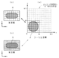
図5および図6は、以上に述べたメッシュ生成部41および画像計算部42の動作を例示する説明図である。図5の例では、図4に例示したメモリ2に画像生成領域Lが設定されている。メッシュ生成部41が生成するメッシュ20は、実空間における画像生成領域Lには、図5(a)が例示するように設定される。空間フィルタ処理が施されない場合、すなわち、ひずみが反映されない場合には、画像計算部42が出力する逆フーリエ像は、例えば図5(b)が示すとおりとなる。図5(b)には、図4(c)に描かれる基本要素12の逆フーリエ像が例示されている。
【0044】
図4(c)に例示される基本要素10,11,12は、レイアウトデータにおいては、図形データとして記述されている。図形データでは、基本要素10,11,12の形状が、例えばそれら各々の角の座標値の組で記述される。これに対して、フーリエ変換部421は、従来周知のようにフーリエ空間に設定されたメッシュ上の画像データとして、フーリエ像を生成する。
【0045】
また、逆フーリエ変換部424は、図5(b)が例示するように、実空間に設定されたメッシュ20上の画像データとして、逆フーリエ像を生成する。図5(b)は、画像データの数値をメッシュ20の区画ごとに例示している。図5(b)の例では、基本要素12が存在する区画では、数値は0であり、存在しない区画では1である。存在する比率に応じて、0〜1の範囲の値が付与されている。
【0046】
図5(b)の例では、ひずみが反映されていないので、逆フーリエ像が表現する基本要素12の形状は、レイアウトデータが表現する基本要素12(図4(c))と同一である。これに対して、空間フィルタ処理が施される場合、すなわち、ひずみが反映される場合には、画像計算部42が出力する逆フーリエ像は、例えば図6が示すとおりとなる。
【0047】
図1〜3に戻って、画像計算部42が出力する画像データである逆フーリエ像は、図形変換部43によって、レイアウトデータと同様の図形データの形式へと変換される(S25)。図形補正部50は、図形変換部43が出力する図形とレイアウトデータが規定する図形とを比較することにより、ひずみを抑制する方向へ、レイアウトデータが規定する図形を補正し、マスクデータとして出力する(S3)。
【0048】
例えば、画像計算部42による計算の結果、大きく仕上がると予想される部分については、アンダーサイジング、逆に小さく仕上がると予想される部分にはオーバーサイジングを行うことにより、総合的なプロセスマージンの向上が図られる。図7は補正後の基本要素12bの形状を例示する説明図である。図7の例では、ひずみがないときの基本要素12の形状が図5(b)のとおりであり、ひずみを考慮したときの基本要素12aの形状が、図6のとおりであるため、ひずみを抑制ないし解消するために、図7が示すように図形補正が行われる。なお、図形補正部50の構成および動作については、文献1に詳細に開示されており、周知技術の一つであるので、その詳細な説明は略する。
【0049】
マスク生成装置61は、図形補正部50が出力するマスクデータにもとづいて、転写用マスクを生成する(S4)。光転写装置62は、半導体装置の材料としての半導体基板の表面に形成されたレジストへ、転写用マスクを転写する(S5)。周知のように、転写後のレジストは、転写されたパターン形状にパターニングされる。基板エッチング装置63は、パターニングされたレジストを遮蔽体として用いることにより、半導体基板へ選択的エッチング処理を施す(S6)。CMP装置またはエッチバック装置64は、選択的エッチング処理が施された半導体基板の上に堆積された膜に対して、CMP(化学的機械的研磨)またはエッチバック処理を施す(S7)。このような各種の処理を経ることにより、半導体装置が製品へと完成される。
【0050】
以上のように、本実施の形態のマスクデータ補正装置29では、階層構造にもとづいて、基本要素のフーリエ像を合成することにより図形全体のフーリエ像が得られるので、図形に大量の基本要素が含まれるマスクデータの補正が、精度を保ちつつ高能率で達成される。
【0051】
実施の形態2.
本実施の形態では、画像計算部42に反映される製造プロセス上の様々なひずみについて説明する。一例として、製造対象としての装置が半導体装置である場合を取り上げるが、液晶表示装置など他の装置の製造プロセスにおいても、同様のひずみを想定することができ、画像計算部42へ反映させることが可能である。これらのひずみを空間フィルタ部423へ反映させる技術、および図形補正装置50でひずみを抑制させる技術それ自体は、従来周知である。
【0052】
図8は、マスク生成装置61の周知の構成例を示す部分切取斜視図である。LaB6電子銃610で生成された電子ビームは、可変成型レンズ部61aを構成する第1成形アパーチャ611、第1成形レンズ612、第1成形偏向器613、第2成形レンズ614、第2成形アパーチャ615、縮小レンズ616およびブランキング電極617を通過した後、収束偏向レンズ部61bを構成する偏向器618および縮小レンズ619を経て、転写用マスク60の上の一点に収束する。マスク生成装置61へ入力されるマスクデータにもとづいて、転写用マスク60には、マスクデータが表現する図形が描画される。
【0053】
このとき、マスクデータが表現する図形と、転写用マスク60に描画される図形との間には、描画ひずみE1(図3)が生じる。転写用マスク60に描画される図形は、電子ビームのエネルギーの蓄積分布像に相当する。電子ビームの代わりに、レーザビームを用いた場合には、描画される図形はレーザビームのエネルギー蓄積分布像に相当する。マスクデータ補正装置29では、これらのエネルギー蓄積分布像を用いて、近接補正を行うことができ、それにより描画ひずみE1を抑制ないし解消することができる。
【0054】
図9は、光転写装置62の周知の構成例を示す説明図である。なお、本明細書において、転写マスクの転写に用いられる「光」は、紫外線等をも包含する電磁波を広く代表する。ランプ620で生成された光は、ミラー621、レンズ622、フライアイ623、レンズ622a、二次光源板625、レンズ622b、ミラー621a、レンズ622c、転写マスク60、レンズ622d、ひとみ面626およびレンズ622eを経ることにより、半導体基板(半導体ウェハ)100の表面に照射される。これにより、転写マスク60の図形が半導体基板100の表面へ転写される。このとき、転写用マスク60に描画される図形と半導体基板100の表面の転写像との間には、転写ひずみE2(図3)が生じる。マスクデータ補正装置29では、光学像を用いて光近接補正を行うことができ、それにより転写ひずみE2を抑制ないし解消することができる。
【0055】
図10は、半導体装置の製造プロセスを例示する製造工程図である。この製造プロセスでは、はじめに半導体基板100が準備され(図10(a))、つぎに半導体基板100の主面の上にレジスト101が塗布される(図10(b))。その後、光転写装置62を用いることにより、転写用マスクの図形が、レジスト101に転写され、現像処理を施すことによってレジストパターン102が形成される(図10(c))。
【0056】
つぎに、レジストパターン102を遮蔽体として用いることにより、半導体基板100の主面に選択的エッチングが施される(図10(d))。このときに形成されるエッチングパターンには、転写像からのひずみであるエッチングひずみE3(図3)が生じる。マスクデータ補正装置29では、エッチングにおけるマイクロローディング効果像を用いて、近接補正を行うことができ、それによりエッチングひずみE3を抑制ないし解消することができる。
【0057】
つづいて、等方的デポジションが施されることにより、エッチング後の半導体基板100を覆うように膜104が堆積される(図10(e))。図10(e)が示すように、膜104の表面には、エッチングパターンに対応した凹凸が形成される。その後、CMPを施すことにより、半導体基板100の主面が露出するまで膜104が研磨される(図10(f))。
【0058】
図11は、CMPを実行するためのCMP装置64の周知の構成例を示す平面図である。回転するテーブル640の上に半導体基板100が載置されており、半導体基板100はテーブル640の上でさらに自転する。図11では、半導体基板100のチップ形成領域110が矩形で描かれている。テーブル640の上方には図示しない研磨布が取り付けられており、この研磨布は半導体基板100の各々の主面へ押圧されている。そして、テーブル640の公転と半導体基板100の自転との二つの回転モードを通じて、半導体基板100の主面が、研磨布との機械的摩擦、および薬液の化学作用によって研磨される。
【0059】
図10(f)に戻って、エッチングパターンに粗密が存在すると、研磨パターンを有する膜105に、半導体基板100の主面の法線方向に沿った研磨ひずみE4が生じる。マスクデータ補正装置29では、研磨像を用いてCMP補正を行うことができ、それにより研磨ひずみE4を抑制ないし解消することができる。
【0060】
図12は、図10(e)の工程の後に、CMPの代わりにエッチバック処理を施す工程を示す製造工程図である。この工程によって、膜105のエッチバックパターンには、半導体基板100の主面の法線方向に沿ったエッチバックひずみE5が生じる。マスクデータ補正装置29では、エッチバック像を用いて補正を行うことができ、それによりエッチバックひずみE5を抑制ないし解消することができる。
【0061】
実施の形態3.
図13は、フーリエ変換部421の好ましい内部構成を示すブロック図である。また、図14は、フーリエ変換部421によるフーリエ変換(S241)の好ましい内部フローを示すフローチャートである。図13が示すフーリエ変換部421は、図形分割部4211および要素図形フーリエ変換部4212を備えている。また、図形分割部4211は、三角形分割部4213、四角形分割部4214および円形分割部4215を備えている。これらの分割部4213,4214,4215にはレイアウトデータが入力される。
【0062】
フーリエ変換(S241)が開始されると、三角形分割部4213は、レイアウトデータが規定する基本要素を、一つまたは複数の三角形に分割する(S2411)。例えば、図15が示す基本要素10に対して、図16が示すように、直角三角形10aが基本要素10から分離される。これにより、基本要素10には直角多角形10bが残る。
【0063】
つぎに、四角形分割部4214は、基本要素を一つまたは複数の四角形に分割する(S2412)。例えば、図16が示す直角多角形10bから、図17が示すように四角形10c,10dが分離される。このように、基本要素が如何に複雑な多角形であっても、単純な三角形と四角形との集合へと分割することができる。
【0064】
レイアウトデータが規定する基本要素が円をも含む場合には、円形分割部4215によって、円の部分がさらに分離される(S2413)。このようにして、基本要素が、三角形、四角形および円形のいずれかである要素図形の集まりへと分割される。
【0065】
要素図形フーリエ変換部4212は、分割されてなる要素図形の群の各々に対して個別にフーリエ変換を行うことにより、要素図形の群の各々のフーリエ像を得る(S2414)。三角形、四角形および円形はいずれも単純な形状であるため、要素図形フーリエ変換部4212は、簡単な計算を通じてフーリエ変換を容易かつ迅速に遂行することが可能である。要素図形フーリエ変換部4212で得られた要素図形ごとのフーリエ像は、合成部423(図2)によって画像生成領域全体の図形のフーリエ像へと合成される。
【0066】
以上のように、本実施の形態では、三角形と四角形と円形とのいずれかである要素図形の群へと基本要素が分割され、要素図形ごとにフーリエ変換が行われ、その結果を重ね合わせることによって、画像生成領域全体の図形に対するフーリエ像が得られる。このため、基本要素が如何に複雑な形状であっても、短時間でかつ精度を劣化させることなく、画像生成領域全体の図形に対するフーリエ変換が達成される。フーリエ変換には、近似計算は含まれていないので、近似ではない正確なフーリエ像が得られる。
【0067】
また、本実施の形態のフーリエ変換部421は合成部423と組み合わせることによって、マスクデータ補正装置29への用途以外に、一般に複雑な図形に対するフーリエ像を簡単かつ迅速に得るフーリエ変換装置として、様々な分野に応用することも可能である。
【0068】
実施の形態4.
図18は、要素図形フーリエ変換部4212および合成部422の好ましい内部構成を示すブロック図である。また、図19は、要素図形フーリエ変換部4212による処理(S2414)および合成部422による処理(S242)の好ましい内部フローを示すフローチャートである。図18が示す要素図形フーリエ変換部4212は、要素図形の形状に応じた3種の空間周波数成分算出部42121,42122,42123を備えている。空間周波数成分算出部42121,42122,42123には、図形分割部4211(図13)が出力する要素図形データが入力される。また、合成部422は、第1合成部4221および第2合成部4222を備えている。
【0069】
要素図形フーリエ変換部4212に要素図形データが入力されると(S24141)、3種の空間周波数成分算出部42121,42122,42123は、それぞれ、要素図形の中の三角形、四角形および円形に対するフーリエ変換を個別に実行し、それぞれのフーリエ像(すなわち空間周波数成分の集合)を得る(S24142,S24143,S24144)。各空間周波数成分は、実空間でのx、y方向に沿ったフーリエ積分を実行することにより得られる。
【0070】
第1合成部4221は、要素図形ごとのフーリエ像を階層構造にしたがって重ね合わせる(S2421)。これによって、画像生成領域全体の要素図形に対するフーリエ像が、要素図形ごとに得られる。第2合成部4222は、第1合成部4221で得られた要素図形ごとのフーリエ像を重ね合わせる(S2422)。その後、画像生成領域全体の図形に対する処理が終了していなければ(S2422)、処理はステップS24142へ戻り、逆に終了しておれば(S2423)、画像生成領域全体の図形に対するフーリエ像が得られる(S2424)。
【0071】
以上の手順では、一度計算した要素図形のフーリエ積分によって得られた空間周波数成分が、階層構造に従って繰り返し利用される。従って、フーリエ積分の回数および三角関数の演算の回数が著しく低減されるので、フーリエ変換の処理能力が飛躍的に向上する。さらに、大規模のデータがであっても実用的な計算時間で処理できる。また、この階層処理は近似を含んでおらず、厳密計算であるため、計算精度が高い。尚、得られる結果は、階層構造を展開して各図形のフーリエ積分をした場合と全く同じであることが確認されており、計算精度に劣化がないことが実証されている。
【0072】
従来技術である実空間上での重ね合わせによれば、いずれも相関距離の長い(1)電子ビームの前方散乱あるいは後方散乱、(2)光学的な干渉の効果、(3)マイクロローディング効果、(4)研磨布の変形の効果等を正しく導入することは難しいという問題点があった。これに対して、本発明の各実施の形態においては、重ね合わせはフーリエ空間上で行われているので、これらの相関距離の長い効果を正しく反映させることが容易である。
【0073】
実施の形態5.
実施の形態3および4の要素図形フーリエ変換部4212が、要素図形の空間周波数成分を計算する際には、要素図形をビットマップに展開した上で数値積分を行うという、フーリエ変換において通常の手法を採用することができる。しかしながら、フーリエ変換の対象となる図形が、簡単な三角形、四角形または円形であることを生かして、つぎの数1が示すように、フーリエ積分の原始関数F(x)を求め、これを用いて定積分を解析的に算出するという手法を採用することが可能である。それにより、フーリエ変換の精度が向上すると同時に、高速計算が達成される。
【0074】
【数1】

実施の形態6.
図20は、メッシュ生成部41の好ましい内部構成を示すブロック図である。また、図21は、メッシュ生成部41によるメッシュ生成(S23)の好ましい内部フローを示すフローチャートである。図20が示すメッシュ生成部41によるメッシュ生成(S23)が開始されると、最小相関距離算出部411は、製造プロセス条件にもとづいて、製造プロセスにおける最小相関距離を算出する(S231)。最小相関距離は、例えば、光学系の場合には最小解像力Rに相当し、Rは、R=λ/4NAにて与えられる。ここで、λは露光波長、NAは投影レンズの開口数である。
【0076】
つぎに、画像生成領域設定部412によって、画像生成領域L(図5(a))が設定される(S232)。つぎに、メッシュ数最適化部413によって、最適なメッシュ数が決定される。メッシュ幅が最小相関距離を超えない範囲で最も大きく、かつメッシュ数が正の整数となるように、画像生成領域の直交する二方向の各々に沿ったメッシュの数が、最適なメッシュの数として決定される。より好ましくは、メッシュ幅が最小相関距離を超えない範囲で最も大きく、かつメッシュ数nは、n=2i3j5k(i,j,kは0か正の整数)となるように決定される(S234,235)。後者の場合には、2,3,5の倍数で使用できるFFT(高速フーリエ変換)を利用することが可能となる。
【0077】
上記の条件の特別な場合として、n=2i(iは正の整数)を満たすには、つぎの数2の条件を満たすように、仮分割数n0が決定される。ここで、ceilは切り上げ整数化関数である。つぎに、数3にしたがってメッシュ数nを決定すると、メッシュ数が2のべき乗となり、これも高速フーリエ変換(FFT)を利用する上で好都合となる。
【0078】
【数2】
![]()
【数3】
![]()
メッシュ発生部414は、メッシュ数最適化部413で決定されたメッシュの数にしたがってメッシュを発生する(S233)。
【0081】
以上のように、本実施の形態では、必要最小限のメッシュ数が設定できるので、計算精度の観点から必要限度を超えたメッシュを生成することによる無駄な計算を省くことできるので、計算精度を高く維持しつつ処理を高速化することができる。
【0082】
実施の形態7.
実施の形態6にしたがって計算精度上必要最小限のメッシュを用いて計算を行い、その結果を表示させると、人間の視覚の上では粗く感じられる場合がある。このような場合には、アップサンプリングを行うと良い。図22は、このような目的のために図2の空間フィルタ部423と逆フーリエ変換部424との間に介挿されるアップサンプリング部44の内部構成を示すブロック図である。アップサンプリング部44は、メッシュ付加部441および新メッシュデータ設定部442を備えている。また、図23は、アップサンプリング部44による処理の手順を示すフローチャートである。
【0083】
メッシュ付加部441は、空間フィルタ部423から入力される画像データに新たなメッシュを付加する(S261)。新メッシュデータ設定部442は、付加されたメッシュ上の画像データにゼロの値を設定し、メッシュが付加される前の画像データとともに、逆フーリエ変換部424へ出力する(S262)。
【0084】
図24は、メッシュ付加部441および新メッシュデータ設定部442による処理を示す説明図である。フーリエ空間におけるフーリエ像F(図24(a))は、逆フーリエ変換部424による逆フーリエ変換により、実空間上の逆フーリエ像Rへ変換される(図24(b))。これに対し、フーリエ空間においてメッシュを付加し、さらに付加されたメッシュ上の画像データにゼロの値を付加すると(図24(a))、その逆フーリエ像Rは、図24(c)が示すように、図24(b)の画像よりも緻密な画像となる。
【0085】
例えば、フーリエ空間上に新たなメッシュを付加して、2次元で2×2倍のメッシュへとメッシュ数を増加させた場合には、実空間へ逆フーリエ変換したときに、2次元で2×2倍のメッシュへとアップサンプリングされている。メッシュ数を増加させる比率は、一般に任意であるが、例えば2×2倍のように、FFTを利用することができる比率に設定するのが望ましい。
【0086】
以上のように、本実施の形態では、フーリエ空間上でアップサンプリングが行われるので、得られる内挿点は、画像全体を考慮したものとなっており、単なる線形補間よりもなめらかで自然な内挿が実現する。したがって、補間の精度が高いという利点が得られる。
【0087】
実施の形態8.
実施の形態7とは逆に、表示デバイスのメッシュよりも計算メッシュの方が多い場合には、ダウンサンプリングを行うことにより、画質を劣化させることなく表示速度を高めることが可能となる。図25は、このような目的のために図2の空間フィルタ部423と逆フーリエ変換部424との間に介挿されるダウンサンプリング部45の内部構成を示すブロック図である。ダウンサンプリング部45は、メッシュ除去部451を備えている。また、図26は、ダウンサンプリング部45による処理の手順を示すフローチャートである。
【0088】
メッシュ除去部451は、空間フィルタ部423から入力される画像データから一部のメッシュを除去する(S271)。メッシュが除去された画像データは、逆フーリエ変換部424へ出力される。
【0089】
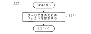
図27は、メッシュ除去部451による処理を示す説明図である。フーリエ空間におけるフーリエ像F(図27(a))は、逆フーリエ変換部424による逆フーリエ変換により、実空間上の逆フーリエ像Rへ変換される(図27(b))。これに対し、フーリエ空間において一部のメッシュが除去されると(図27(a))、その逆フーリエ像Rは、図27(c)が示すように、図27(b)の画像よりも粗い画像となる。
【0090】
例えば、フーリエ空間上のフーリエ像Fの周りの高周波成分を除去して、2次元で1/2×1/2倍のメッシュにした場合には、実空間へ逆フーリエ変換したときに、2次元で1/2×1/2倍のメッシュへとダウンサンプリングされている。メッシュ数を減少させる比率は、一般に任意であるが、例えば1/2×1/2倍のように、FFTを利用することができる比率に設定するのが望ましい。
【0091】
以上のように、本実施の形態では、フーリエ空間上でダウンサンプリングが行われるので、得られる内挿点は、画像全体を考慮したものとなっており、単なる線形補間よりもなめらかで自然な内挿が実現する。また、計算結果の表示速度が速くなるので、システムの操作性が向上する。
【0092】
実施の形態9.
実施の形態1〜8のマスクデータ補正装置29を用いて補正されたマスクデータを用いることにより、安価かつ高精度な転写マスクを得ることができる。この特殊な転写マスクを用いて、半導体集積回路等の半導体装置を製造することにより、安価で信頼性の高い半導体装置を得ることができる。半導体装置に限らず、液晶表示装置など、パターン構造を有する他の装置についても同様である。これらの装置の製造方法については、実施の形態2において図10および図11を参照しつつ詳細に説明がなされているので、さらなる詳細な説明は略する。図3が示すように、図10または図11に例示される工程S5〜S7を経た後に、通常においては幾段階にもわたる処理がさらに行われることにより、製品としての半導体装置、あるいは液晶表示装置などのパターン構造を有する装置が完成する。
【0093】
実施の形態10.
実施の形態7で示したアップサンプリング部44は、フーリエ変換部および逆フーリエ変換部を付加することにより、マスクデータ補正装置29から独立したアップサンプリング装置を構成することが可能である。同様に、実施の形態8で示したダウンサンプリング部45は、フーリエ変換部および逆フーリエ変換部を付加することにより、マスクデータ補正装置29から独立したダウンサンプリング装置を構成することが可能である。本実施の形態では、そのように構成されたアップサンプリング装置およびダウンサンプリング装置について説明する。
【0094】
図28は、本実施の形態によるアップサンプリング装置80の構成例を示すブロック図であり、図29はその処理(S8)の手順を示すフローチャートである。アップサンプリング装置80は、はじめに一次元ないし複数次元の空間内で規定される離散データを受信する(S81)。すると、フーリエ変換部81は、受信した離散データに対してフーリエ変換を施すことにより(S82)、離散データを周波数成分の集合へと変換する。メッシュ付加部82は、周波数成分の集合を上記した一次元ないし複数次元と同一次元のフーリエ空間内に設定されたメッシュ上のデータの集合として、新たなメッシュをフーリエ空間内に付加する(S83)。
【0095】
新メッシュデータ設定部83は、付加されたメッシュ上のデータにゼロの値を設定し、付加される前のメッシュ上のデータとともに出力する(S84)。逆フーリエ変換部84は、新メッシュデータ設定部83が出力するデータに対して逆フーリエ変換を行うことによりアップサンプリングデータを得るとともに(S85)、得られたアップサンプリングデータを出力する(S86)。
【0096】
アップサンプリング装置80では、フーリエ空間内でアップサンプリングが行われるので、離散データの集合の全体を反映した補間が行われる。このため、単なる線型補間などでは得られない、なめらかで自然なアップサンプリング処理後のデータが得られる。
【0097】
図30は、本実施の形態によるダウンサンプリング装置90の構成例を示すブロック図であり、図31はその処理(S9)の手順を示すフローチャートである。ダウンサンプリング装置90は、はじめに一次元ないし複数次元の空間内で規定される離散データを受信する(S81)。すると、フーリエ変換部81は、受信した離散データに対してフーリエ変換を施すことにより(S82)、離散データを周波数成分の集合へと変換する。
【0098】
メッシュ除去部85は、周波数成分の集合を上記した一次元ないし複数次元と同一次元のフーリエ空間内に設定されたメッシュ上のデータの集合として、一部のメッシュをフーリエ空間内で除去した上で出力する(S87)。逆フーリエ変換部84は、メッシュ除去部85が出力するデータに対して逆フーリエ変換を行うことによりダウンサンプリングデータを得るとともに(S85)、得られたダウンサンプリングデータを出力する(S88)。
【0099】
ダウンサンプリング装置90では、フーリエ空間内でダウンサンプリングが行われるので、離散データの集合の全体を反映した補間が行われる。このため、サンプリング数は減少しているものの、単なる線型補間などでは得られない、なめらかで自然なダウンサンプリング処理後のデータが得られる。
【0100】
【発明の効果】
第1の発明の装置では、階層構造にもとづいて、基本要素のフーリエ像を合成することにより図形全体のフーリエ像が得られるので、図形に大量の基本要素が含まれるマスクデータの補正が、精度を保ちつつ高能率で達成される。
【0101】
第2の発明の装置では、描画ひずみを含むひずみを抑制するように補正が行われるので、転写用マスクに現れる描画ひずみを抑制することのできるマスクデータが得られる。
【0102】
第3の発明の装置では、転写ひずみを含むひずみを抑制するように補正が行われるので、転写像に現れる転写ひずみを抑制することのできるマスクデータが得られる。
【0103】
第4の発明の装置では、エッチングひずみを含むひずみを抑制するように補正が行われるので、エッチングパターンに現れるエッチングひずみを抑制することのできるマスクデータを得ることができる。
【0104】
第5の発明の装置では、研磨ひずみを含むひずみを抑制するように補正が行われるので、研磨後のパターンに現れる研磨ひずみを抑制することのできるマスクデータが得られる。
【0105】
第6の発明の装置では、エッチバックひずみを含むひずみを抑制するように補正が行われるので、エッチバック後のパターンに現れるエッチバックひずみを抑制することのできるマスクデータが得られる。
【0106】
第7の発明の装置では、三角形と四角形と円形とのいずれかである要素図形の群へと基本要素が分割され、要素図形ごとにフーリエ変換が行われ、その結果を重ね合わせることによって、図形の全体に対するフーリエ像が得られる。このため、基本要素がいかに複雑な形状であっても、短時間でかつ精度を劣化させることなく、図形の全体に対するフーリエ変換が達成される。その結果、マスクデータの補正が、精度を劣化させることなく、さらに高能率で達成される。
【0107】
第8の発明の装置では、簡単な形状の要素図形の群へと基本要素が分割されることを生かして、空間周波数成分を算出する際に、定積分計算が原始関数を用いて解析的に行われる。このため、フーリエ変換の精度がさらに向上すると同時に、計算に要する時間がさらに短縮される。
【0108】
第9の発明の装置では、メッシュの数が最適化されるので、無駄な計算時間を要することなく、マスクデータの補正が高い精度で達成される。
【0109】
第10の発明の装置では、メッシュの数が高速フーリエ変換に適した個数に制限され、高速フーリエ変換を用いてフーリエ変換が行われるので、精度を劣化させることなく計算の能率が高められる。
【0110】
第11の発明の装置では、フーリエ空間内でアップサンプリングが行われるので、図形の全体を反映した補間が行われる。このため、単なる線型補間などでは得られない、なめらかで自然な補正後のマスクデータが得られる。
【0111】
第12の発明の装置では、フーリエ空間内でダウンサンプリングが行われるので、図形の全体を反映した補間が行われる。このため、メッシュ数は減少しているものの、単なる線型補間などでは得られない、なめらかで自然な補正後のマスクデータが得られる。
【0112】
第13の発明の製造方法では、本発明のマスクデータ補正装置を用いてマスクデータが生成され、このマスクデータを用いて転写用マスクが形成されるので、精度の高い転写用マスクが高能率で得られる。
【0113】
第14の発明の製造方法では、本発明のマスクデータ補正装置を用いてマスクデータが生成され、このマスクデータを用いて転写用マスクが形成され、さらに、この転写用マスクを用いて、レジストへの転写、レジストのパターニング、および選択的処理が施されるので、高精度のパターン構造を有する装置が高能率で得られる。
【図面の簡単な説明】
【図1】 実施の形態による各種の製造装置のブロック図である。
【図2】 図1の画像計算部42の内部構成を示すブロック図である。
【図3】 図1の各種の製造装置による製造プロセスを示す流れ図である。
【図4】 実施の形態1による処理の説明図である。
【図5】 画像計算部42による動作の説明図である。
【図6】 画像計算部42による動作の説明図である。
【図7】 図形補正装置50による動作の説明図である。
【図8】 マスク生成装置61の構成例を示す部分切取斜視図である。
【図9】 光転写装置62の構成例を示す説明図である。
【図10】 半導体装置の製造プロセスを例示する製造工程図である。
【図11】 CMP装置64の構成例を示す平面図である。
【図12】 半導体装置の製造プロセスを例示する製造工程図である。
【図13】 フーリエ変換部421の内部構成を示すブロック図である。
【図14】 フーリエ変換部421による処理を示す流れ図である。
【図15】 フーリエ変換部421による処理を示す動作説明図である。
【図16】 フーリエ変換部421による処理を示す動作説明図である。
【図17】 フーリエ変換部421による処理を示す動作説明図である。
【図18】 要素図形フーリエ変換部4212および合成部422の内部構成を示すブロック図である。
【図19】 要素図形フーリエ変換部4212および合成部422による処理を示す流れ図である。
【図20】 メッシュ生成部41の内部構成を示すブロック図である。
【図21】 メッシュ生成部41による処理を示す流れ図である。
【図22】 アップサンプリング部44の内部構成を示すブロック図である。
【図23】 アップサンプリング部44による処理を示す流れ図である。
【図24】 アップサンプリング部44による処理を示す動作説明図である。
【図25】 ダウンサンプリング部45の内部構成を示すブロック図である。
【図26】 ダウンサンプリング部45による処理を示す流れ図である。
【図27】 ダウンサンプリング部45による処理を示す動作説明図である。
【図28】 アップサンプリング装置80の構成を示すブロック図である。
【図29】 アップサンプリング装置80による処理を示す流れ図である。
【図30】 ダウンサンプリング装置90の構成を示すブロック図である。
【図31】 ダウンサンプリング装置90による処理を示す流れ図である。
【図32】 従来のマスクデータ補正方法の手順を示す流れ図である。
【図33】 従来のマスクデータ補正方法で採用される階層構造の一例を示す説明図である。
【符号の説明】
10,11,12 基本要素、10a,10c,10d 要素図形、20 メッシュ、29 マスクデータ補正装置、41 メッシュ生成部、411 最小相関距離算出部、413 メッシュ数最適化部、421 図形分割部、4212 要素図形フーリエ変換部、422 合成部、423 空間フィルタ部、43 図形変換部、451 メッシュ除去部、50 図形補正装置(図形補正部)、60転写用マスク、80 アップサンプリング装置、81,421 フーリエ変換部、82,441 メッシュ付加部、83,442 新メッシュデータ設定部、84,424 逆フーリエ変換部、90 ダウンサンプリング装置、100 半導体基板(材料)、102 レジストパターン、104 膜、E1 描画ひずみ、E2 転写ひずみ、E3 エッチングひずみ、E4 研磨ひずみ、E5 エッチバックひずみ、F フーリエ像、F(x) 原始関数、L 画像生成領域、R
逆フーリエ像。[0001]
BACKGROUND OF THE INVENTION
The present invention relates to a mask data correction device, a Fourier transform device, an upsampling device, a downsampling device, a method for manufacturing a transfer mask, and a method for manufacturing a device having a pattern structure, and in particular, improves efficiency while maintaining accuracy. For improvements.
[0002]
[Prior art]
In recent years, there has been remarkable progress in miniaturization of large-scale integrated circuits (LSIs), and the development of microfabrication technology has made this possible. Among them, the optical transfer technology is still at the center of the microfabrication technology due to the high throughput by batch exposure and the achievements of the optical technology that has been cultivated for 100 years.
[0003]
However, at the present time when the processing dimension of the fine pattern has become smaller than the wavelength of the exposure light, it is important to identify the limitations of the optical transfer technology and overcome the limitations of resolution and depth of focus. In order to perform such an analysis, a technique for calculating an optical image, a technique for correcting distortion generated from the calculated optical image, and the like have attracted particular attention in recent years. FIG. 32 is a flow chart showing the procedure of a mask data correction method disclosed in Japanese Patent Laid-Open No. 8-297769 (hereinafter referred to as Document 1) as an example of the invention of the present inventor.
[0004]
This method is disclosed in detail in
[0005]
Furthermore, when using these techniques, it is necessary to pay attention to the deterioration of the optical image caused by the aberration of the optical system. The details of this technique are described in Japanese Patent Application Laid-Open No. 9-167731 (hereinafter referred to as Reference 2) or Japanese Patent Application Laid-Open No. 10-335224 (hereinafter referred to as Reference 3), both of which are the inventions of the present inventors. . In addition, there are cases where full-shot level long-range correlation becomes a problem.
[0006]
In order to perform these evaluations or optimizations, it is necessary to examine the correspondence between the calculation results related to the optical image and the experimental results in various cases. However, the calculation related to the optical image generally requires a large amount of calculation, such as the need to perform inverse Fourier transform after Fourier transform of the mask figure. Therefore, many proposals have been made to execute the Fourier transform at high speed. Common things are:
(1) Fast Fourier Transformation (FFT) (for example, “Waveform Data Processing for Scientific Measurements” described in Shigeo Minami, CQ Publisher);
(2) OCA (Optical Coherent Approximation) (for example, described in YC Pali and T. Kailath J. OP Soc. Am A, Vol. 11 (1994) 2438);
(3) Unequally spaced Fourier transform (eg, E. Barouch, B. Bradie, U. Hollerbach, and SA Orszag, J. Vac. Sci. And Technol. B8 (1990) 1432; E. Barouch, B. Bradie, U Hollerbach, and SAOrszag, Proc. SPIE Vol.1465 (1991) 254; E. Barouch, U. Hollerbach, SAOrszag, B. Bradie and M. Peckcrar, IEEE Electron Device Lett., EDL-12 (1991) 513, etc. Description);
(4) Partial copyrent approximation (for example, M. Yeung: Proc, Kodak Microelectoronics Seminar INTERFACE '85 (KTI Chemicals, Inc, San Diego, 1986) p. 115; M. Yeung: Proc. SPIE Vol. 922 (1988) 149); and
(5) Massively parallel operations (for example, K, Kamon, W. Wakamiya, H. Nagata, K. Moriizumi, T, Miyamoto, Y, Myoi and M. Tanaka; Proc, SPIE Vol. 2512 (1995) 491; T .Hanawa, K.kamon, A.Nakae, S.Nakao, and K.Moriizumi: Proc, SPIE Vol.2726 (1996) 640; A.Nakae, K.Kamon, T.Hanawa, K.Moriizumi and S.Nakao : Jpn.J.Appl.phys.Vol.35 (1996) 6395 etc.) is known.
[0007]
In recent years, remarkable speedup has been promoted through these technologies. Each of these technologies is a very effective technology, and made a great contribution to the innovation of microfabrication technology. However, it is still not enough to combine them for LSI full-shot calculations. . This is because, as an example, a 1G (Gigabit) DRAM currently under development is formed by laying a huge number of 1G transistors vertically and horizontally to form a memory cell array. Even a logic device (logic circuit) has a structure including a large number of small RAMs. In addition, it is considered that LSIs will continue to be highly integrated.
[0008]
Conventionally, a technique (for example, dracula of cadence) that processes graphic data after flat development once has been common. On the other hand, in order to handle a large number of figures, a device that performs operations such as layout verification using the hierarchical structure of figure data (eg, arant hercules; menter caliber; lucent clover, etc.) Has been developed recently. In these apparatuses, as shown in FIG. 33, some data is collected in a
[0009]
Since these devices can execute simple calculations and comparisons between figures quickly, they are suitable for applications such as design rule checking, simple logic calculations between figures, or sizing.
[0010]
[Problems to be solved by the invention]
However, in the case where the influence or correlation of a certain figure spreads over a plurality of cells, each element cell must be expanded, so that not only the data processing speed cannot be achieved but also the processing capability is rather reduced. It is known that even deterioration may occur.
[0011]
On the other hand, in the application of optical image calculation, the influence of a certain figure extends within the coherence distance of the optical system. In addition, the microloading effect in dry etching or the proximity effect in mask drawing may reach about 10 μm. Therefore, it is necessary to calculate how the graphic elements interfere with each other or influence each other. Rather, it can be said that it is essential to calculate the state of this correlation in various process simulations including lithography. In general, this optical coherence or various proximity effects often extend over a plurality of cells, and conventionally, it has been necessary to evaluate the cells by fully developing them. Therefore, there is a problem that even if the hierarchized data is used for the proximity correction calculation, all the data must be finally expanded, and the effectiveness of the hierarchical processing cannot be fully exhibited.
[0012]
The present invention has been made to solve the above-described problems in the prior art, and mask data that can effectively use the hierarchical structure of layout data to increase the efficiency of processing while maintaining high accuracy. Correction device , Roll It is an object of the present invention to provide a method for manufacturing a transfer mask and a method for manufacturing a device having a pattern structure.
[0013]
[Means for Solving the Problems]
The apparatus according to the first aspect of the present invention provides a pattern shape of a transfer mask used in a manufacturing process based on the shape of basic elements of a figure having a hierarchical structure, layout data defining the hierarchical structure, and manufacturing process conditions. A mask data correction apparatus that generates mask data to be expressed in a form that suppresses distortion predicted in a manufacturing process, and a Fourier transform unit that obtains a Fourier image of the basic element by Fourier transforming the basic element; A synthesis unit that obtains a Fourier image of the figure by synthesizing the Fourier image of the basic element in Fourier space based on the hierarchical structure, and a spatial filter corresponding to the distortion with respect to the Fourier image of the figure A spatial filter unit that performs processing, and an inverse Fourier transform for the Fourier image that has been subjected to the spatial filter processing. The distortion is suppressed by comparing the graphic output by the graphic conversion unit and the graphic defined by the layout data with an inverse Fourier transform unit that obtains an inverse Fourier image reflecting the distortion. A graphic correction unit that corrects the graphic defined by the layout data in a direction to be output and outputs it as the mask data.
[0014]
In the apparatus of the second invention, in the mask data correction apparatus of the first invention, the distortion includes a drawing distortion generated when the transfer mask is formed using electron beam drawing based on the mask data.
[0015]
In the apparatus of the third invention, in the mask data correction apparatus of the first or second invention, when the distortion is transferred using the transfer mask formed based on the mask data, a transfer image is obtained. Including transcription distortion.
[0016]
According to a fourth invention, in the mask data correction device according to any one of the first to third inventions, the distortion is formed by transferring the transfer mask formed based on the mask data. When selective etching is performed using a resist pattern, the etching distortion generated in the etching pattern is included.
[0017]
According to a fifth invention, in the mask data correction device according to any one of the first to fourth inventions, the distortion is formed by transferring the transfer mask formed based on the mask data. After performing selective etching using the resist pattern, it includes polishing strain generated in the pattern after polishing when the polishing process is performed on the deposited film.
[0018]
According to a sixth invention, in the mask data correction device according to any one of the first to fourth inventions, the distortion is formed by transferring the transfer mask formed based on the mask data. After performing selective etching using the resist pattern, this includes etching back strain that occurs in the pattern after the etch back when performing an etch back process on the deposited film.
[0019]
According to a seventh aspect of the present invention, in the mask data correction device according to any one of the first to sixth aspects of the invention, the Fourier transform unit may be an element figure that is one of a triangle, a quadrangle, and a circle. A figure dividing unit that divides into groups, and an element figure Fourier transform unit that obtains a Fourier image of each of the group of element figures by individually performing a Fourier transform on each of the group of element figures .
[0020]
According to an eighth aspect of the present invention, in the mask data correction apparatus according to the seventh aspect of the present invention, when the element figure Fourier transform unit calculates a spatial frequency component in order to obtain the Fourier image, an analytical function is used using a primitive function. Perform a definite integral calculation.
[0021]
According to a ninth aspect of the invention, there is provided the mask data correction device according to any one of the first to eighth aspects, wherein an image generation area is set in the real space and the Fourier space, and a mesh is set in the image generation area. A generation unit, and the mesh generation unit is a minimum correlation distance calculation unit that calculates a minimum correlation distance in the manufacturing process based on the manufacturing process condition; and a mesh width that is the largest in a range in which the mesh width does not exceed the minimum correlation distance. A mesh number optimizing unit that determines the number of meshes along each of two orthogonal directions of the image generation region so that the number of meshes is a positive integer.
[0022]
In an apparatus according to a tenth aspect, in the mask data correction apparatus according to the ninth aspect, the mesh number optimization unit sets the positive integer to n = 2. i 3 j 5 k (I, j, k are all 0 or a positive integer), and the Fourier transform unit performs the Fourier transform using fast Fourier transform.
[0023]
According to an eleventh aspect of the invention, in the mask data correction device according to any one of the first to eighth aspects of the invention, an image generation area is set in the real space and the Fourier space, and a mesh is set in the image generation area. A generating unit, a mesh adding unit for adding a new mesh to the image data after the spatial filter processing, a value of zero is set for the image data on the added mesh, and the mesh before the mesh is added A new mesh data setting unit that outputs the image data together with the image data, and the inverse Fourier transform unit performs the inverse Fourier transform on the image data output by the new mesh data setting unit.
[0024]
According to a twelfth aspect of the invention, in the mask data correction device according to any one of the first to eighth aspects of the invention, an image generation area is set in the real space and the Fourier space, and a mesh is set in the image generation area. A generation unit; and a mesh removal unit that removes a part of the mesh from the image data after the spatial filter processing, wherein the inverse Fourier transform unit performs the inverse operation on the image data output by the mesh removal unit. Perform Fourier transform.
[0025]
A manufacturing method of a thirteenth invention is a method for manufacturing a transfer mask, wherein (a) generating the mask data using the mask data correction device according to any one of the first to twelfth inventions; b) forming a transfer mask using the mask data generated in the step (a).
[0026]
A manufacturing method of a fourteenth invention is a method of manufacturing a device having a pattern structure, and (a) a step of generating the mask data using the mask data correcting device of any of the first to twelfth inventions. (B) a step of forming a transfer mask using the mask data generated in the step (a), (c) a step of forming a resist on the surface of the material of the apparatus as a manufacturing target, and (d) Transferring the transfer mask formed in the step (b) to the resist; (e) patterning the resist in the pattern shape transferred in the step (d); and (f) patterned. And a step of selectively processing the material by using the resist as a shield.
[0030]
DETAILED DESCRIPTION OF THE INVENTION
FIG. 1 is a block diagram showing the configuration of various manufacturing apparatuses that execute the manufacturing process of the present embodiment from circuit design to product shipment of devices (for example, semiconductor devices and liquid crystal display devices) to be manufactured. FIG. 2 is a block diagram showing an internal configuration of the
[0031]
Hereinafter, the apparatus and method of the present embodiment will be described with reference to FIGS. It should be noted that each element other than the
[0032]
When the manufacturing process of the device to be manufactured is started, layout data representing the original drawing is created by the original drawing creating device 30 (S1). Here, the original figure means the figure before the figure correction to be compared with the figure after the figure correction (S3) is applied. In the original
[0033]
Thereafter, the
[0034]
In a large-scale integrated circuit, many basic elements are often arranged in an array in a circuit element such as a memory cell array. If the layout data of such a circuit is stored in the form of basic elements + hierarchical structure, the storage capacity of the storage medium can be saved, which is efficient. For this reason, the layout data of the large-scale integrated circuit is stored as data defining the shape and hierarchical structure of the basic elements of a figure having a hierarchical structure.
[0035]
FIG. 4 is an explanatory diagram illustrating a hierarchical structure in the layout data. In the example of FIG. 4, the
[0036]
Next, when graphic correction is not performed (S1a), the layout data is used as it is as mask data for forming a transfer mask. On the other hand, when graphic correction is performed (S1a), the mask
[0037]
In the image generation (S2), first, layout data having a hierarchical structure is input from the layout data storage medium 33 (S21), and further process conditions (that is, conditions relating to the manufacturing process) are input from the outside (S22). Process conditions include, for example, a transfer mask drawing method (electron beam drawing, laser drawing, low reflection mask type, phase shift method type), and exposure apparatus optical parameters (wavelength, numerical aperture, numerical aperture ratio σ, super Resolution type, etc.), conditions relating to resist (pre-baking, PEB, negative / positive, novolac system, chemical amplification system, dry / wet phenomenon, etc.), etching conditions (dry / wet etc.), etc.
[0038]
Next, the
[0039]
Next, image calculation is performed by the image calculation unit 42 (S24). In the image calculation (S24), first, a Fourier transform unit 421 (FIG. 2) performs Fourier transform on the basic elements defined in the layout data, thereby obtaining a Fourier image of the basic elements. Next, a Fourier image of the graphic of the entire image generation region is obtained by superimposing the Fourier images of the basic elements in the Fourier space based on the hierarchical structure defined in the layout data by the synthesis unit 422 (S242). .
[0040]
Subsequently, the
[0041]
Spatial filtering itself corresponding to various distortions is a well-known technique. For example, in order to consider the influence of the numerical aperture of the optical system, a circular low-pass filter process may be performed. In addition, in order to consider the direction dependency in the characteristics of the manufacturing apparatus, elliptical filtering may be performed.
[0042]
Next, the inverse
[0043]
5 and 6 are explanatory diagrams illustrating the operations of the
[0044]
The
[0045]
Further, as illustrated in FIG. 5B, the inverse
[0046]
In the example of FIG. 5B, since distortion is not reflected, the shape of the
[0047]
1-3, the inverse Fourier image, which is the image data output by the
[0048]
For example, as a result of the calculation by the
[0049]
The
[0050]
As described above, in the mask
[0051]
In the present embodiment, various distortions in the manufacturing process reflected in the
[0052]
FIG. 8 is a partially cutaway perspective view showing a known configuration example of the
[0053]
At this time, a drawing distortion E1 (FIG. 3) occurs between the figure represented by the mask data and the figure drawn on the
[0054]
FIG. 9 is an explanatory diagram illustrating a known configuration example of the
[0055]
FIG. 10 is a manufacturing process diagram illustrating the manufacturing process of the semiconductor device. In this manufacturing process, first, the
[0056]
Next, selective etching is performed on the main surface of the
[0057]
Subsequently, by performing isotropic deposition, a
[0058]
FIG. 11 is a plan view showing a known configuration example of a
[0059]
Returning to FIG. 10 (f), if the etching pattern has a density, a polishing
[0060]
FIG. 12 is a manufacturing process diagram showing a process of performing an etch-back process instead of CMP after the process of FIG. By this step, an etch-back strain E5 along the normal direction of the main surface of the
[0061]
Embodiment 3 FIG.
FIG. 13 is a block diagram illustrating a preferred internal configuration of the
[0062]
When the Fourier transform (S241) is started, the
[0063]
Next, the
[0064]
If the basic element defined by the layout data also includes a circle, the
[0065]
The element graphic
[0066]
As described above, in this embodiment, basic elements are divided into groups of element figures that are either triangles, quadrangles, or circles, Fourier transforms are performed for each element figure, and the results are superimposed. As a result, a Fourier image for the graphic of the entire image generation region is obtained. For this reason, no matter how complex the basic elements are, a Fourier transform can be achieved for a figure in the entire image generation region in a short time and without degrading accuracy. Since the Fourier transform does not include approximate calculation, an accurate Fourier image that is not approximate can be obtained.
[0067]
In addition to the application to the mask
[0068]
FIG. 18 is a block diagram showing a preferable internal configuration of the element figure
[0069]
When element graphic data is input to the element graphic Fourier transform unit 4212 (S24141), the three types of spatial frequency
[0070]
The
[0071]
In the above procedure, the spatial frequency obtained by Fourier integration of the element figure once calculated component Are repeatedly used according to the hierarchical structure. Therefore, the number of times of Fourier integration and the number of operations of trigonometric functions are remarkably reduced, so that the processing capability of Fourier transform is dramatically improved. Furthermore, even large-scale data can be processed in a practical calculation time. In addition, this hierarchical processing does not include approximation and is a strict calculation, so the calculation accuracy is high. The obtained results are confirmed to be exactly the same as when the hierarchical structure is expanded and Fourier integration of each figure is performed, and it is proved that there is no deterioration in calculation accuracy.
[0072]
According to the superposition in the real space which is the prior art, all have a long correlation distance (1) electron beam forward scattering or back scattering, (2) optical interference effect, (3) microloading effect, (4) There is a problem that it is difficult to correctly introduce the deformation effect of the polishing cloth. On the other hand, in each embodiment of the present invention, since the superposition is performed in the Fourier space, it is easy to correctly reflect the effect of these long correlation distances.
[0073]
The element graphic
[0074]
[Expression 1]
FIG. 20 is a block diagram illustrating a preferable internal configuration of the
[0076]
Next, the image generation area L (FIG. 5A) is set by the image generation area setting unit 412 (S232). Next, an optimal mesh number is determined by the mesh
[0077]
As a special case of the above condition, n = 2 i In order to satisfy (i is a positive integer), the number of provisional divisions so as to satisfy the
[0078]
[Expression 2]
![]()
[Equation 3]
![]()
The
[0081]
As described above, in the present embodiment, since the minimum number of meshes can be set, it is possible to omit useless calculation by generating meshes exceeding the necessary limit from the viewpoint of calculation accuracy, so that the calculation accuracy can be reduced. Processing can be speeded up while maintaining high.
[0082]
When calculation is performed using the minimum mesh necessary for calculation accuracy according to the sixth embodiment and the result is displayed, it may feel rough on human vision. In such a case, upsampling may be performed. FIG. 22 is a block diagram showing an internal configuration of the
[0083]
The
[0084]
FIG. 24 is an explanatory diagram showing processing by the
[0085]
For example, when a new mesh is added to the Fourier space and the number of meshes is increased to 2 × 2 times in 2 dimensions, 2 × Upsampled to 2x mesh. The ratio for increasing the number of meshes is generally arbitrary, but it is desirable to set the ratio so that FFT can be used, for example, 2 × 2.
[0086]
As described above, in this embodiment, since upsampling is performed in the Fourier space, the obtained interpolation point takes into consideration the entire image, and is smoother and more natural than simple linear interpolation. Insertion is realized. Therefore, there is an advantage that the interpolation accuracy is high.
[0087]
Contrary to
[0088]
The
[0089]
FIG. 27 is an explanatory diagram showing processing by the
[0090]
For example, when the high-frequency components around the Fourier image F in the Fourier space are removed and the mesh is two-dimensionally ½ × ½ times, when the inverse Fourier transform is performed to the real space, the two-dimensional Is downsampled to 1/2 × 1/2 times mesh. The ratio for reducing the number of meshes is generally arbitrary, but it is desirable to set the ratio at which FFT can be used, such as 1/2 × 1/2.
[0091]
As described above, in the present embodiment, since the downsampling is performed in the Fourier space, the interpolation point to be obtained considers the entire image, and is smoother and more natural than simple linear interpolation. Insertion is realized. In addition, since the display speed of the calculation result is increased, the operability of the system is improved.
[0092]
By using the mask data corrected using the mask
[0093]
The
[0094]
FIG. 28 is a block diagram illustrating a configuration example of the
[0095]
The new mesh
[0096]
In the
[0097]
FIG. 30 is a block diagram illustrating a configuration example of the
[0098]
The
[0099]
In the
[0100]
【The invention's effect】
In the apparatus of the first invention, the Fourier image of the entire figure can be obtained by synthesizing the Fourier images of the basic elements based on the hierarchical structure. Achieved with high efficiency while maintaining.
[0101]
In the apparatus according to the second aspect of the invention, correction is performed so as to suppress distortion including drawing distortion, so that mask data that can suppress drawing distortion appearing on the transfer mask can be obtained.
[0102]
In the apparatus according to the third aspect of the invention, correction is performed so as to suppress distortion including transfer distortion, so that mask data capable of suppressing transfer distortion appearing in the transfer image is obtained.
[0103]
In the apparatus according to the fourth aspect of the invention, correction is performed so as to suppress distortion including etching distortion, so that mask data that can suppress etching distortion appearing in the etching pattern can be obtained.
[0104]
In the apparatus according to the fifth aspect of the invention, correction is performed so as to suppress strain including polishing strain, so that mask data that can suppress polishing strain appearing in the pattern after polishing is obtained.
[0105]
In the apparatus according to the sixth aspect of the invention, correction is performed so as to suppress distortion including etch back distortion, so that mask data capable of suppressing the etch back distortion appearing in the pattern after the etch back is obtained.
[0106]
In the apparatus of the seventh invention, the basic elements are divided into groups of element figures that are either triangles, quadrangles, or circles, Fourier transforms are performed for each element figure, and the results are superimposed to form a figure. A Fourier image of the whole is obtained. For this reason, no matter how complex the basic elements are, the Fourier transform of the entire figure can be achieved in a short time and without degrading accuracy. As a result, the correction of the mask data is achieved with higher efficiency without degrading the accuracy.
[0107]
In the apparatus of the eighth invention, the definite integral calculation is analytically performed using a primitive function when calculating the spatial frequency component by taking advantage of the fact that the basic elements are divided into groups of element figures having simple shapes. Done. For this reason, the time required for calculation is further shortened while the accuracy of Fourier transform is further improved.
[0108]
In the ninth aspect of the invention, since the number of meshes is optimized, mask data correction is achieved with high accuracy without requiring unnecessary calculation time.
[0109]
In the apparatus of the tenth invention, the number of meshes is limited to the number suitable for the fast Fourier transform, and the Fourier transform is performed using the fast Fourier transform, so that the calculation efficiency is improved without degrading the accuracy.
[0110]
In the device of the eleventh aspect, since upsampling is performed in Fourier space, interpolation that reflects the entire figure is performed. Therefore, smooth and natural corrected mask data that cannot be obtained by simple linear interpolation or the like can be obtained.
[0111]
In the twelfth aspect of the invention, downsampling is performed in Fourier space, so that interpolation that reflects the entire figure is performed. For this reason, although the number of meshes is reduced, smooth and natural corrected mask data can be obtained which cannot be obtained by simple linear interpolation or the like.
[0112]
In the manufacturing method of the thirteenth invention, mask data is generated using the mask data correction apparatus of the present invention, and a transfer mask is formed using this mask data. Therefore, a highly accurate transfer mask is highly efficient. can get.
[0113]
In the manufacturing method of the fourteenth invention, mask data is generated using the mask data correction device of the present invention, a transfer mask is formed using the mask data, and further, the transfer mask is used to form a resist. Therefore, an apparatus having a highly accurate pattern structure can be obtained with high efficiency.
[Brief description of the drawings]
FIG. 1 is a block diagram of various manufacturing apparatuses according to an embodiment.
2 is a block diagram showing an internal configuration of an
FIG. 3 is a flowchart showing manufacturing processes by various manufacturing apparatuses in FIG. 1;
4 is an explanatory diagram of processing according to
FIG. 5 is an explanatory diagram of an operation by the
6 is an explanatory diagram of an operation by an
FIG. 7 is an explanatory diagram of an operation performed by the
FIG. 8 is a partially cutaway perspective view showing a configuration example of a
FIG. 9 is an explanatory diagram showing a configuration example of the
FIG. 10 is a manufacturing process diagram illustrating the manufacturing process for the semiconductor device;
11 is a plan view showing a configuration example of a
FIG. 12 is a manufacturing process diagram illustrating the manufacturing process for a semiconductor device;
13 is a block diagram showing an internal configuration of a
FIG. 14 is a flowchart showing processing by a
FIG. 15 is an operation explanatory diagram showing processing by the
FIG. 16 is an operation explanatory diagram showing processing by the
FIG. 17 is an operation explanatory diagram showing processing by a
18 is a block diagram showing the internal configuration of an element graphic
FIG. 19 is a flowchart showing processing by an element graphic
20 is a block diagram showing an internal configuration of a
FIG. 21 is a flowchart showing processing by the
22 is a block diagram showing an internal configuration of an
23 is a flowchart showing processing by the
24 is an operation explanatory diagram showing processing by the
25 is a block diagram showing an internal configuration of a
26 is a flowchart showing processing by the
FIG. 27 is an operation explanatory diagram showing processing by the
28 is a block diagram showing a configuration of an
29 is a flowchart showing processing by the
30 is a block diagram showing a configuration of a
FIG. 31 is a flowchart showing processing by the
FIG. 32 is a flowchart showing a procedure of a conventional mask data correction method.
FIG. 33 is an explanatory diagram showing an example of a hierarchical structure employed in a conventional mask data correction method.
[Explanation of symbols]
10, 11, 12 Basic element, 10a, 10c, 10d Element graphic, 20 mesh, 29 Mask data correction device, 41 Mesh generation unit, 411 Minimum correlation distance calculation unit, 413 Mesh number optimization unit, 421 Graphic division unit, 4212 Element graphic Fourier transform unit, 422 synthesis unit, 423 spatial filter unit, 43 graphic conversion unit, 451 mesh removal unit, 50 graphic correction device (graphic correction unit), 60 transfer mask, 80 upsampling device, 81, 421 Fourier transform Part, 82,441 mesh adding part, 83,442 new mesh data setting part, 84,424 inverse Fourier transform part, 90 downsampling device, 100 semiconductor substrate (material), 102 resist pattern, 104 film, E1 drawing distortion, E2 Transfer strain, E3 etching strain, E4 polishing strain , E5 etch back strain, F Fourier image, F (x) primitive, L image generating region, R
Inverse Fourier image.
Claims (14)
前記基本要素をフーリエ変換することにより前記基本要素のフーリエ像を得るフーリエ変換部と、
前記階層構造にもとづいて前記基本要素の前記フーリエ像をフーリエ空間内で合成することにより前記図形のフーリエ像を得る合成部と、
前記図形の前記フーリエ像に対して、前記ひずみに対応した空間フィルタ処理を施す空間フィルタ部と、
前記空間フィルタ処理を施された前記フーリエ像に対して、逆フーリエ変換を行うことにより、前記ひずみを反映した逆フーリエ像を得る逆フーリエ変換部と、
前記逆フーリエ像を図形へ変換する図形変換部と、
前記図形変換部が出力する前記図形と前記レイアウトデータが規定する前記図形とを比較することにより、前記ひずみを抑制する方向へ、前記レイアウトデータが規定する前記図形を補正し、前記マスクデータとして出力する図形補正部と、を備えるマスクデータ補正装置。Mask data representing the pattern shape of a transfer mask used in the manufacturing process based on layout data defining the shape of the basic elements of the figure having a hierarchical structure, the hierarchical structure, and the manufacturing process conditions. A mask data correction device that generates the distortion predicted by
A Fourier transform unit that obtains a Fourier image of the basic element by Fourier transforming the basic element;
A synthesis unit that obtains a Fourier image of the figure by synthesizing the Fourier image of the basic element in Fourier space based on the hierarchical structure;
A spatial filter unit that performs a spatial filter process corresponding to the distortion on the Fourier image of the figure;
An inverse Fourier transform unit that obtains an inverse Fourier image reflecting the distortion by performing inverse Fourier transform on the Fourier image subjected to the spatial filter processing;
A graphic converter for converting the inverse Fourier image into a graphic;
By comparing the graphic output by the graphic conversion unit with the graphic specified by the layout data, the graphic specified by the layout data is corrected in a direction to suppress the distortion and output as the mask data. A mask data correction device comprising:
前記基本要素を、三角形と四角形と円形とのいずれかである要素図形の群へと分割する図形分割部と、
前記要素図形の群の各々に対して個別にフーリエ変換を行うことにより、前記要素図形の群の各々のフーリエ像を得る要素図形フーリエ変換部と、を備える請求項1ないし請求項6のいずれかに記載のマスクデータ補正装置。The Fourier transform unit is
A figure dividing unit that divides the basic element into a group of element figures that are either a triangle, a square, or a circle;
7. An element graphic Fourier transform unit that obtains a Fourier image of each of the element graphic groups by individually performing a Fourier transform on each of the element graphic groups. The mask data correction apparatus described in 1.
前記メッシュ生成部は、
前記製造プロセス条件にもとづいて、前記製造プロセスにおける最小相関距離を算出する最小相関距離算出部と、
メッシュ幅が前記最小相関距離を超えない範囲で最も大きく、かつメッシュ数が正の整数となるように、前記画像生成領域の直交する二方向の各々に沿ったメッシュの数を決定するメッシュ数最適化部と、を備える、請求項1ないし請求項8のいずれかに記載のマスクデータ補正装置。It further includes a mesh generation unit that sets an image generation region in the real space and the Fourier space, and sets a mesh in the image generation region,
The mesh generation unit
Based on the manufacturing process conditions, a minimum correlation distance calculating unit that calculates a minimum correlation distance in the manufacturing process;
Optimum number of meshes that determines the number of meshes along each of the two orthogonal directions of the image generation region so that the mesh width is the largest within a range not exceeding the minimum correlation distance and the number of meshes is a positive integer. The mask data correction device according to claim 1, further comprising: a conversion unit.
前記フーリエ変換部が、高速フーリエ変換を用いて前記フーリエ変換を行う、請求項9に記載のマスクデータ補正装置。The mesh number optimization unit limits the positive integer to a positive integer n defined by n = 2 i 3 j 5 k (where i, j, and k are all 0 or a positive integer),
The mask data correction apparatus according to claim 9, wherein the Fourier transform unit performs the Fourier transform using fast Fourier transform.
前記空間フィルタ処理後の画像データに新たなメッシュを付加するメッシュ付加部と、
付加された前記メッシュ上の画像データにゼロの値を設定し、前記メッシュが付加される前の前記画像データとともに出力する新メッシュデータ設定部と、をさらに備え、
前記逆フーリエ変換部は、前記新メッシュデータ設定部が出力する画像データに対して前記逆フーリエ変換を行う、請求項1ないし請求項8のいずれかに記載のマスクデータ補正装置。A mesh generation unit that sets an image generation region in the real space and the Fourier space, and sets a mesh in the image generation region;
A mesh adding unit for adding a new mesh to the image data after the spatial filter processing;
A new mesh data setting unit that sets a value of zero to the image data on the added mesh and outputs the image data together with the image data before the mesh is added;
The mask data correction device according to claim 1, wherein the inverse Fourier transform unit performs the inverse Fourier transform on the image data output from the new mesh data setting unit.
前記空間フィルタ処理後の画像データから一部のメッシュを除去するメッシュ除去部とを、さらに備え、
前記逆フーリエ変換部は、前記メッシュ除去部が出力する画像データに対して前記逆フーリエ変換を行う、請求項1ないし請求項8のいずれかに記載のマスクデータ補正装置。A mesh generation unit that sets an image generation region in the real space and the Fourier space, and sets a mesh in the image generation region;
A mesh removing unit for removing a part of the mesh from the image data after the spatial filter processing,
The mask data correction apparatus according to claim 1, wherein the inverse Fourier transform unit performs the inverse Fourier transform on the image data output from the mesh removal unit.
(b)前記工程(a)で生成されたマスクデータを用いて転写用マスクを形成する工程と、を備える転写用マスクの製造方法。(a) generating the mask data using the mask data correction apparatus according to any one of claims 1 to 12;
(b) forming a transfer mask using the mask data generated in the step (a), and a transfer mask manufacturing method.
(b)前記工程(a)で生成されたマスクデータを用いて転写用マスクを形成する工程と、
(c)製造対象としての装置の材料の表面にレジストを形成する工程と、
(d)前記工程(b)で形成された転写用マスクを前記レジストへ転写する工程と、
(e)前記工程(d)で転写されたパターン形状に前記レジストをパターニングする工程と、
(f)パターニングされた前記レジストを遮蔽体として用いることにより、前記材料へ選択的処理を施す工程とを備える、パターン構造を有する装置の製造方法。(a) generating the mask data using the mask data correction apparatus according to any one of claims 1 to 12;
(b) forming a transfer mask using the mask data generated in the step (a);
(c) a step of forming a resist on the surface of the material of the device to be manufactured;
(d) transferring the transfer mask formed in the step (b) to the resist;
(e) patterning the resist in the pattern shape transferred in the step (d);
(f) A method of manufacturing an apparatus having a pattern structure, comprising: using the patterned resist as a shield, and performing a selective treatment on the material.
Priority Applications (5)
| Application Number | Priority Date | Filing Date | Title |
|---|---|---|---|
| JP2000214002A JP4671473B2 (en) | 2000-07-14 | 2000-07-14 | Mask data correction apparatus, method for manufacturing transfer mask, and method for manufacturing apparatus having pattern structure |
| TW090108272A TW492070B (en) | 2000-07-14 | 2001-04-06 | Mask data correction apparatus, Fourier transformation apparatus, up sampling apparatus, down sampling apparatus, method of manufacturing transfer mask, and method of manufacturing device having pattern structure |
| US09/827,903 US6831997B2 (en) | 2000-07-14 | 2001-04-09 | Mask data correction apparatus, fourier transformation apparatus, up sampling apparatus, down sampling apparatus, method of manufacturing transfer mask, and method of manufacturing device having pattern structure |
| KR10-2001-0025149A KR100385804B1 (en) | 2000-07-14 | 2001-05-09 | Mask data correction apparatus, fourier transformation apparatus, up sampling apparatus, down sampling apparatus, method of manufacturing transfer mask, and method of manufacturing device having pattern structure |
| DE10122678A DE10122678A1 (en) | 2000-07-14 | 2001-05-10 | Mask data correction device with graphic correction stage generates transfer mask pattern shape for use in manufacturing process so as to prevent faults anticipated during manufacture |
Applications Claiming Priority (1)
| Application Number | Priority Date | Filing Date | Title |
|---|---|---|---|
| JP2000214002A JP4671473B2 (en) | 2000-07-14 | 2000-07-14 | Mask data correction apparatus, method for manufacturing transfer mask, and method for manufacturing apparatus having pattern structure |
Related Child Applications (1)
| Application Number | Title | Priority Date | Filing Date |
|---|---|---|---|
| JP2010165825A Division JP2011019233A (en) | 2010-07-23 | 2010-07-23 | Upsampling device and downsampling device |
Publications (3)
| Publication Number | Publication Date |
|---|---|
| JP2002031882A JP2002031882A (en) | 2002-01-31 |
| JP2002031882A5 JP2002031882A5 (en) | 2007-08-02 |
| JP4671473B2 true JP4671473B2 (en) | 2011-04-20 |
Family
ID=18709661
Family Applications (1)
| Application Number | Title | Priority Date | Filing Date |
|---|---|---|---|
| JP2000214002A Expired - Fee Related JP4671473B2 (en) | 2000-07-14 | 2000-07-14 | Mask data correction apparatus, method for manufacturing transfer mask, and method for manufacturing apparatus having pattern structure |
Country Status (5)
| Country | Link |
|---|---|
| US (1) | US6831997B2 (en) |
| JP (1) | JP4671473B2 (en) |
| KR (1) | KR100385804B1 (en) |
| DE (1) | DE10122678A1 (en) |
| TW (1) | TW492070B (en) |
Cited By (1)
| Publication number | Priority date | Publication date | Assignee | Title |
|---|---|---|---|---|
| CN111580359A (en) * | 2020-04-29 | 2020-08-25 | 中国科学院光电技术研究所 | Intelligent correction device control system for super-resolution lithography precision mask |
Families Citing this family (11)
| Publication number | Priority date | Publication date | Assignee | Title |
|---|---|---|---|---|
| US20020123866A1 (en) * | 2001-01-05 | 2002-09-05 | Lin Benjamin Szu-Min | Optical proximity correction algorithm for pattern transfer |
| JP4156221B2 (en) * | 2001-10-11 | 2008-09-24 | 大日本印刷株式会社 | Optical structure |
| US7233887B2 (en) * | 2002-01-18 | 2007-06-19 | Smith Bruce W | Method of photomask correction and its optimization using localized frequency analysis |
| US7457736B2 (en) * | 2002-11-21 | 2008-11-25 | Synopsys, Inc. | Automated creation of metrology recipes |
| US7315636B2 (en) * | 2003-09-18 | 2008-01-01 | Accuray, Inc. | Generation of reconstructed images |
| JP4562374B2 (en) * | 2003-10-27 | 2010-10-13 | ルネサスエレクトロニクス株式会社 | Mask data correction device for transfer |
| DE10355264B4 (en) * | 2003-11-26 | 2008-08-14 | Qimonda Ag | Method for improving a simulation model of the photolithographic projection |
| KR100846633B1 (en) * | 2006-11-09 | 2008-07-16 | 삼성전자주식회사 | Method and apparatus for detecting defects of patterns |
| US7923815B2 (en) * | 2008-01-07 | 2011-04-12 | International Business Machines Corporation | DRAM having deep trench capacitors with lightly doped buried plates |
| JP5159501B2 (en) * | 2008-08-06 | 2013-03-06 | キヤノン株式会社 | Master data creation program, master data creation method, master creation method, exposure method, and device manufacturing method |
| US8392009B2 (en) * | 2009-03-31 | 2013-03-05 | Taiwan Semiconductor Manufacturing Company, Ltd. | Advanced process control with novel sampling policy |
Citations (10)
| Publication number | Priority date | Publication date | Assignee | Title |
|---|---|---|---|---|
| JPH05107726A (en) * | 1991-10-21 | 1993-04-30 | Mitsubishi Electric Corp | Verification device for design data on phase shift mask |
| JPH06204112A (en) * | 1992-12-30 | 1994-07-22 | Sony Corp | Method and device for exposure |
| JPH07128138A (en) * | 1993-10-29 | 1995-05-19 | Nec Corp | Method of optical intensity distribution analysis |
| JPH08297692A (en) * | 1994-09-16 | 1996-11-12 | Mitsubishi Electric Corp | Device and method for correcting optical proximity, and pattern forming method |
| JPH09167731A (en) * | 1995-12-14 | 1997-06-24 | Mitsubishi Electric Corp | Projection aligner, mask pattern for evaluating aberration, method for evaluating aberration, filter for removing aberration and production of semiconductor device |
| JPH10282635A (en) * | 1997-04-09 | 1998-10-23 | Sony Corp | Method for correcting pattern data, electron beam writing method, photomask and its manufacture, exposure method, semiconductor device and its production and pattern data correcting device |
| JPH10335224A (en) * | 1997-06-02 | 1998-12-18 | Mitsubishi Electric Corp | Apparatus and method for projection exposure, amplitude aberration evaluating mask pattern, amplitude aberration evaluation method and amplitude aberration filter |
| JPH11110585A (en) * | 1997-10-06 | 1999-04-23 | Oki Electric Ind Co Ltd | Three-dimensional image display and its data eliminating method |
| US6171731B1 (en) * | 1999-01-20 | 2001-01-09 | Lsi Logic Corporation | Hybrid aerial image simulation |
| WO2001054046A1 (en) * | 2000-01-20 | 2001-07-26 | Lsi Logic Corporation | Geometric aerial image simulation |
Family Cites Families (10)
| Publication number | Priority date | Publication date | Assignee | Title |
|---|---|---|---|---|
| JPS61221963A (en) | 1985-03-28 | 1986-10-02 | Toshiba Corp | Fourier transfor device |
| JP3245882B2 (en) * | 1990-10-24 | 2002-01-15 | 株式会社日立製作所 | Pattern forming method and projection exposure apparatus |
| JP3343919B2 (en) * | 1991-08-22 | 2002-11-11 | 株式会社ニコン | Mask, circuit element manufacturing method and exposure method |
| JPH06163351A (en) * | 1992-11-20 | 1994-06-10 | Mitsubishi Electric Corp | Projection exposure device |
| JP3418768B2 (en) | 1994-04-18 | 2003-06-23 | 大日本印刷株式会社 | Arithmetic processing method of integrated circuit mask pattern data |
| US6078738A (en) * | 1997-05-08 | 2000-06-20 | Lsi Logic Corporation | Comparing aerial image to SEM of photoresist or substrate pattern for masking process characterization |
| US6091845A (en) * | 1998-02-24 | 2000-07-18 | Micron Technology, Inc. | Inspection technique of photomask |
| JPH11272724A (en) | 1998-03-20 | 1999-10-08 | Matsushita Electric Ind Co Ltd | Processing method and processor for hierarchical data |
| US6263299B1 (en) * | 1999-01-19 | 2001-07-17 | Lsi Logic Corporation | Geometric aerial image simulation |
| US6496597B1 (en) * | 1999-03-03 | 2002-12-17 | Autodesk Canada Inc. | Generating image data |
-
2000
- 2000-07-14 JP JP2000214002A patent/JP4671473B2/en not_active Expired - Fee Related
-
2001
- 2001-04-06 TW TW090108272A patent/TW492070B/en not_active IP Right Cessation
- 2001-04-09 US US09/827,903 patent/US6831997B2/en not_active Expired - Lifetime
- 2001-05-09 KR KR10-2001-0025149A patent/KR100385804B1/en not_active IP Right Cessation
- 2001-05-10 DE DE10122678A patent/DE10122678A1/en not_active Ceased
Patent Citations (10)
| Publication number | Priority date | Publication date | Assignee | Title |
|---|---|---|---|---|
| JPH05107726A (en) * | 1991-10-21 | 1993-04-30 | Mitsubishi Electric Corp | Verification device for design data on phase shift mask |
| JPH06204112A (en) * | 1992-12-30 | 1994-07-22 | Sony Corp | Method and device for exposure |
| JPH07128138A (en) * | 1993-10-29 | 1995-05-19 | Nec Corp | Method of optical intensity distribution analysis |
| JPH08297692A (en) * | 1994-09-16 | 1996-11-12 | Mitsubishi Electric Corp | Device and method for correcting optical proximity, and pattern forming method |
| JPH09167731A (en) * | 1995-12-14 | 1997-06-24 | Mitsubishi Electric Corp | Projection aligner, mask pattern for evaluating aberration, method for evaluating aberration, filter for removing aberration and production of semiconductor device |
| JPH10282635A (en) * | 1997-04-09 | 1998-10-23 | Sony Corp | Method for correcting pattern data, electron beam writing method, photomask and its manufacture, exposure method, semiconductor device and its production and pattern data correcting device |
| JPH10335224A (en) * | 1997-06-02 | 1998-12-18 | Mitsubishi Electric Corp | Apparatus and method for projection exposure, amplitude aberration evaluating mask pattern, amplitude aberration evaluation method and amplitude aberration filter |
| JPH11110585A (en) * | 1997-10-06 | 1999-04-23 | Oki Electric Ind Co Ltd | Three-dimensional image display and its data eliminating method |
| US6171731B1 (en) * | 1999-01-20 | 2001-01-09 | Lsi Logic Corporation | Hybrid aerial image simulation |
| WO2001054046A1 (en) * | 2000-01-20 | 2001-07-26 | Lsi Logic Corporation | Geometric aerial image simulation |
Cited By (1)
| Publication number | Priority date | Publication date | Assignee | Title |
|---|---|---|---|---|
| CN111580359A (en) * | 2020-04-29 | 2020-08-25 | 中国科学院光电技术研究所 | Intelligent correction device control system for super-resolution lithography precision mask |
Also Published As
| Publication number | Publication date |
|---|---|
| JP2002031882A (en) | 2002-01-31 |
| DE10122678A1 (en) | 2002-01-31 |
| KR20020007983A (en) | 2002-01-29 |
| KR100385804B1 (en) | 2003-06-02 |
| US20020018599A1 (en) | 2002-02-14 |
| US6831997B2 (en) | 2004-12-14 |
| TW492070B (en) | 2002-06-21 |
Similar Documents
| Publication | Publication Date | Title |
|---|---|---|
| JP4738012B2 (en) | Optical proximity correction based on fast model | |
| JP5057555B2 (en) | System and method for minimizing print line shape distortion by illumination and reticle optimization | |
| JP4671473B2 (en) | Mask data correction apparatus, method for manufacturing transfer mask, and method for manufacturing apparatus having pattern structure | |
| JP5685371B2 (en) | Method for simulating aspects of a lithographic process | |
| US7921383B1 (en) | Photolithographic process simulation including efficient result computation for multiple process variation values | |
| US20170147734A1 (en) | Tool to provide integrated circuit masks with accurate dimensional compensation of patterns | |
| JP4430595B2 (en) | Method for identifying extreme interaction pitch region, method for manufacturing a mask, and computer program | |
| US8285030B2 (en) | Determining calibration parameters for a lithographic process | |
| US20130346037A1 (en) | Lithography Modeling And Applications | |
| JP5086926B2 (en) | Calculation method, program, and exposure method | |
| TW200931191A (en) | Calculation method, generation method, program, exposure method, and mask fabrication method | |
| JPH08335552A (en) | Method of optimizing illumination and projective image formation device | |
| US8238644B2 (en) | Fast method to model photoresist images using focus blur and resist blur | |
| US20060048091A1 (en) | Method for correcting position-dependent distortions in patterning of integrated circuits | |
| US20130322777A1 (en) | High-Accuracy Centered Fractional Fourier Transform Matrix for Optical Imaging and Other Applications | |
| EP0307726B1 (en) | Semiconductor manufacturing process which compensates for the distortion between a pattern on a semiconductor body and the mask from which the pattern is derived | |
| Rosenbluth et al. | Fast calculation of images for high numerical aperture lithography | |
| JP2011019233A (en) | Upsampling device and downsampling device | |
| KR20200140361A (en) | How to determine the electromagnetic field associated with a computational lithography mask model | |
| JP2021166271A (en) | Mask information adjustment device, mask data adjustment method, program | |
| TWI840340B (en) | Method and system for reticle enhancement technology | |
| JP4921536B2 (en) | Program and calculation method | |
| Chen et al. | Abbe singular-value decomposition: Compact Abbe’s kernel generation for microlithography aerial image simulation using singular-value decomposition method | |
| JP3792681B2 (en) | How to create mask drawing data | |
| Chiang et al. | Abbe-SVD: compact Abbe’s kernel generation for microlithography aerial image simulation using singular-value decomposition method |
Legal Events
| Date | Code | Title | Description |
|---|---|---|---|
| A521 | Written amendment |
Free format text: JAPANESE INTERMEDIATE CODE: A523 Effective date: 20070612 |
|
| A621 | Written request for application examination |
Free format text: JAPANESE INTERMEDIATE CODE: A621 Effective date: 20070612 |
|
| RD04 | Notification of resignation of power of attorney |
Free format text: JAPANESE INTERMEDIATE CODE: A7424 Effective date: 20091218 |
|
| A711 | Notification of change in applicant |
Free format text: JAPANESE INTERMEDIATE CODE: A712 Effective date: 20100524 |
|
| A977 | Report on retrieval |
Free format text: JAPANESE INTERMEDIATE CODE: A971007 Effective date: 20100611 |
|
| A131 | Notification of reasons for refusal |
Free format text: JAPANESE INTERMEDIATE CODE: A131 Effective date: 20100615 |
|
| A521 | Written amendment |
Free format text: JAPANESE INTERMEDIATE CODE: A523 Effective date: 20100723 |
|
| TRDD | Decision of grant or rejection written | ||
| A01 | Written decision to grant a patent or to grant a registration (utility model) |
Free format text: JAPANESE INTERMEDIATE CODE: A01 Effective date: 20110118 |
|
| A01 | Written decision to grant a patent or to grant a registration (utility model) |
Free format text: JAPANESE INTERMEDIATE CODE: A01 |
|
| A61 | First payment of annual fees (during grant procedure) |
Free format text: JAPANESE INTERMEDIATE CODE: A61 Effective date: 20110118 |
|
| R150 | Certificate of patent or registration of utility model |
Free format text: JAPANESE INTERMEDIATE CODE: R150 |
|
| FPAY | Renewal fee payment (event date is renewal date of database) |
Free format text: PAYMENT UNTIL: 20140128 Year of fee payment: 3 |
|
| S531 | Written request for registration of change of domicile |
Free format text: JAPANESE INTERMEDIATE CODE: R313531 |
|
| R350 | Written notification of registration of transfer |
Free format text: JAPANESE INTERMEDIATE CODE: R350 |
|
| LAPS | Cancellation because of no payment of annual fees |