JP4669803B2 - Integrated circuit and signal processing apparatus using the same - Google Patents
Integrated circuit and signal processing apparatus using the same Download PDFInfo
- Publication number
- JP4669803B2 JP4669803B2 JP2006080796A JP2006080796A JP4669803B2 JP 4669803 B2 JP4669803 B2 JP 4669803B2 JP 2006080796 A JP2006080796 A JP 2006080796A JP 2006080796 A JP2006080796 A JP 2006080796A JP 4669803 B2 JP4669803 B2 JP 4669803B2
- Authority
- JP
- Japan
- Prior art keywords
- power supply
- supply voltage
- clock
- integrated circuit
- supplied
- Prior art date
- Legal status (The legal status is an assumption and is not a legal conclusion. Google has not performed a legal analysis and makes no representation as to the accuracy of the status listed.)
- Expired - Fee Related
Links
Images


Classifications
-
- G—PHYSICS
- G06—COMPUTING; CALCULATING OR COUNTING
- G06F—ELECTRIC DIGITAL DATA PROCESSING
- G06F1/00—Details not covered by groups G06F3/00 - G06F13/00 and G06F21/00
- G06F1/26—Power supply means, e.g. regulation thereof
- G06F1/32—Means for saving power
-
- G—PHYSICS
- G06—COMPUTING; CALCULATING OR COUNTING
- G06F—ELECTRIC DIGITAL DATA PROCESSING
- G06F1/00—Details not covered by groups G06F3/00 - G06F13/00 and G06F21/00
- G06F1/26—Power supply means, e.g. regulation thereof
- G06F1/32—Means for saving power
- G06F1/3203—Power management, i.e. event-based initiation of a power-saving mode
-
- G—PHYSICS
- G06—COMPUTING; CALCULATING OR COUNTING
- G06F—ELECTRIC DIGITAL DATA PROCESSING
- G06F1/00—Details not covered by groups G06F3/00 - G06F13/00 and G06F21/00
- G06F1/26—Power supply means, e.g. regulation thereof
-
- G—PHYSICS
- G06—COMPUTING; CALCULATING OR COUNTING
- G06F—ELECTRIC DIGITAL DATA PROCESSING
- G06F1/00—Details not covered by groups G06F3/00 - G06F13/00 and G06F21/00
- G06F1/26—Power supply means, e.g. regulation thereof
- G06F1/28—Supervision thereof, e.g. detecting power-supply failure by out of limits supervision
-
- G—PHYSICS
- G06—COMPUTING; CALCULATING OR COUNTING
- G06F—ELECTRIC DIGITAL DATA PROCESSING
- G06F1/00—Details not covered by groups G06F3/00 - G06F13/00 and G06F21/00
- G06F1/26—Power supply means, e.g. regulation thereof
- G06F1/32—Means for saving power
- G06F1/3203—Power management, i.e. event-based initiation of a power-saving mode
- G06F1/3206—Monitoring of events, devices or parameters that trigger a change in power modality
- G06F1/3209—Monitoring remote activity, e.g. over telephone lines or network connections
-
- G—PHYSICS
- G06—COMPUTING; CALCULATING OR COUNTING
- G06F—ELECTRIC DIGITAL DATA PROCESSING
- G06F1/00—Details not covered by groups G06F3/00 - G06F13/00 and G06F21/00
- G06F1/26—Power supply means, e.g. regulation thereof
- G06F1/32—Means for saving power
- G06F1/3203—Power management, i.e. event-based initiation of a power-saving mode
- G06F1/3234—Power saving characterised by the action undertaken
- G06F1/324—Power saving characterised by the action undertaken by lowering clock frequency
-
- G—PHYSICS
- G06—COMPUTING; CALCULATING OR COUNTING
- G06F—ELECTRIC DIGITAL DATA PROCESSING
- G06F1/00—Details not covered by groups G06F3/00 - G06F13/00 and G06F21/00
- G06F1/26—Power supply means, e.g. regulation thereof
- G06F1/32—Means for saving power
- G06F1/3203—Power management, i.e. event-based initiation of a power-saving mode
- G06F1/3234—Power saving characterised by the action undertaken
- G06F1/3296—Power saving characterised by the action undertaken by lowering the supply or operating voltage
-
- Y—GENERAL TAGGING OF NEW TECHNOLOGICAL DEVELOPMENTS; GENERAL TAGGING OF CROSS-SECTIONAL TECHNOLOGIES SPANNING OVER SEVERAL SECTIONS OF THE IPC; TECHNICAL SUBJECTS COVERED BY FORMER USPC CROSS-REFERENCE ART COLLECTIONS [XRACs] AND DIGESTS
- Y02—TECHNOLOGIES OR APPLICATIONS FOR MITIGATION OR ADAPTATION AGAINST CLIMATE CHANGE
- Y02D—CLIMATE CHANGE MITIGATION TECHNOLOGIES IN INFORMATION AND COMMUNICATION TECHNOLOGIES [ICT], I.E. INFORMATION AND COMMUNICATION TECHNOLOGIES AIMING AT THE REDUCTION OF THEIR OWN ENERGY USE
- Y02D10/00—Energy efficient computing, e.g. low power processors, power management or thermal management
Landscapes
- Engineering & Computer Science (AREA)
- Theoretical Computer Science (AREA)
- Physics & Mathematics (AREA)
- General Engineering & Computer Science (AREA)
- General Physics & Mathematics (AREA)
- Power Sources (AREA)
- Semiconductor Integrated Circuits (AREA)
Description
本発明は、集積回路及びそれを用いた信号処理装置に関する。 The present invention relates to an integrated circuit and a signal processing apparatus using the integrated circuit.
近年のエレクトロニクス技術の伸展に伴って、携帯オーディオ再生機器、携帯電話、携帯型ゲーム、PDA(Personal Digital Assistants)等といった持ち運び便利な携帯性を売りとし且つ所望のアプリケーションに係る信号処理を実行する信号処理装置の普及がめざましい。かかる信号処理装置は、二次電池(ニッケル水素充電池、リチウムイオン充電池等)や一次電池(アルカリ乾電池、マンガン乾電池等)によって構成された内部電源を搭載することで携帯性を実現している(例えば、以下に示す特許文献1を参照)。
ところで、内部電源の電源電圧のみで所望のアプリケーションを長時間実行すると、当然の結果として内部電源の電力消費は増大する。従って、信号処理装置は、多種多様なアプリケーションを長時間実行させる意味で、さらなる低消費電力化の対策が必須となっており、既存の対策では不十分であった。 By the way, if a desired application is executed for a long time using only the power supply voltage of the internal power supply, the power consumption of the internal power supply naturally increases. Therefore, in the signal processing apparatus, a measure for further reducing power consumption is indispensable in order to execute a wide variety of applications for a long time, and existing measures are insufficient.
前述した課題を解決するための主たる本発明は、第1の電源電圧を供給する外部電源が印加されて動作する集積回路において、前記外部電源から供給される前記第1の電源電圧のレベルを監視して前記外部電源から前記第1の電源電圧が供給されているか否かを判定する電源電圧監視部と、第1の周波数の第1のクロック及び前記第1の周波数よりも低い第2の周波数を有する第2のクロックが供給され、前記電源電圧監視部において、前記第1の電源電圧が供給されている旨が判定された場合には前記第1のクロックを選択し、前記第1の電源電圧が供給されていない旨が判定された場合には前記第2のクロックを選択し出力するクロック選択部と、前記クロック選択部が出力する前記第1のクロック又は前記第2のクロックのうちいずれか一方の供給を受けて動作し、前記集積回路の動作を制御するプロセッサと、を備える。 A main aspect of the present invention for solving the above-described problem is to monitor a level of the first power supply voltage supplied from the external power supply in an integrated circuit that operates by applying an external power supply that supplies the first power supply voltage. A power supply voltage monitoring unit for determining whether or not the first power supply voltage is supplied from the external power supply, a first clock having a first frequency, and a second frequency lower than the first frequency. And when the power supply voltage monitoring unit determines that the first power supply voltage is supplied, the first clock is selected and the first power supply is selected. When it is determined that no voltage is supplied, the clock selection unit selects and outputs the second clock, and the first clock or the second clock output by the clock selection unit It operates by receiving one of the supply, and a processor for controlling the operation of the integrated circuit.
本発明によれば、外部電源の供給状況に応じて供給する電源電圧を適切に制御することにより、集積回路における電力消費を低減することができる。 According to the present invention, it is possible to reduce power consumption in an integrated circuit by appropriately controlling a power supply voltage to be supplied in accordance with a supply status of an external power supply.
<信号処理装置の外部接続>
図1は、本発明に係る信号処理装置の外部接続を説明するための図である。以下では、本発明に係る信号処理装置の一例として、USB(Universal Serial Bus)インタフェース101を備えており、パーソナルコンピュータ300からUSBケーブル400のデータライン401を介して転送された圧縮オーディオデータのデジタル再生を行う携帯オーディオ再生機器100を採りあげて説明する。なお、本発明に係る信号処理装置としては、例えば、携帯電話、携帯ゲーム、PDA等であってもよい。
<External connection of signal processor>
FIG. 1 is a diagram for explaining external connections of a signal processing apparatus according to the present invention. Hereinafter, as an example of the signal processing apparatus according to the present invention, a USB (Universal Serial Bus)
ここで、USBとは、共通のUSBインタフェースで様々なタイプの信号処理装置をUSBホスト機器へと接続可能なシリアルインタフェース規格のことである。USBの現時点での最新バージョンは「USB2.0」であり、LS(Low Speed)、FS(Full Speed)及びHS(High Speed)の3種類の転送モードを備えており、用途に応じて3種類の転送モードが使い分けられる。また、USBは、ハブを利用することで最大127個のUSB機器をツリー状に接続可能であり、また、USBホスト機器の電源を投入した状態で新たなUSB機器を接続可能な所謂ホットプラグに対応している。 Here, USB is a serial interface standard that allows various types of signal processing devices to be connected to a USB host device through a common USB interface. The latest version of USB at the moment is “USB2.0”, which has three types of transfer modes: LS (Low Speed), FS (Full Speed), and HS (High Speed). Different transfer modes are used. In addition, USB can connect up to 127 USB devices in a tree shape by using a hub, and is a so-called hot plug that can connect a new USB device with the USB host device powered on. It corresponds.
まず、パーソナルコンピュータ300は、USBコントローラ310並びにUSBインタフェース320を備えてある場合とする。この場合、パーソナルコンピュータ300のUSBインタフェース320と、携帯オーディオ再生機器100のUSBインタフェース101との間を、USBケーブル400によって接続することで、パーソナルコンピュータ300と携帯オーディオ再生機器100間がUSB接続される。なお、USBケーブル400は、2本のデータライン401と、電源ライン402と、GNDライン403とによって構成されており、USBインタフェース320、101は、それぞれ、一対のデータ端子D+及びD−と、電源端子VBUSと、GND端子とが設けられる。
First, it is assumed that the
パーソナルコンピュータ300は、電源プラグ361を介して供給されるAC電源電圧をDC電源電圧へと変換する電源アダプタ360を備えるとともに、全体の制御を司るCPU330、様々なプログラムを格納するROM等のメモリ340、音楽ファイルや動画ファイル等を格納するハードディスク350、が相互に通信可能に接続されている。ここで、ハードディスク350に格納される音楽ファイルは、例えば、MPEG−1 Audio Layer3(MP3)形式等の圧縮オーディオデータであり、ハードディスク350に格納される動画ファイルは、例えば、MPEG−2形式、MPEG−4形式等の圧縮ムービーデータである。
The
ここで、パーソナルコンピュータ300から携帯オーディオ再生機器100に向けての音楽ファイルのデータ転送の概要を説明する。まず、パーソナルコンピュータ300は、メモリ340に格納されたプログラムを起動し、ポーリング要求等によって携帯オーディオ再生機器100を自身に接続されたUSB機器として認識する。そして、パーソナルコンピュータ300は、ハードディスク350から任意の音楽ファイルを読み出し、USBコントローラ310へと転送する。USBコントローラ310は、ハードディスク350から読み出された音楽ファイルをパケット形式へと変換して、USBインタフェース320乃至USBケーブル400を介して携帯オーディオ再生機器100へと差動の半二重伝送を行うためのUSB規格に準拠した通信プロトコル処理を行う。この結果、携帯オーディオ再生機器100は、パーソナルコンピュータ300から音楽ファイルを取り込むことができる。
Here, an outline of music file data transfer from the
一方、携帯オーディオ再生機器100は、パーソナルコンピュータ300から音楽ファイルのデータ転送が完了した場合、一般的には、USBインタフェース101からUSBケーブル400を取り外した上で、当該音楽ファイルの再生処理を実行することになる。しかし、音楽ファイルのデータ転送が完了した場合に、USBインタフェース101にUSBケーブル400を接続したままの状態であっても、携帯オーディオ再生機器100は、音楽ファイルの再生処理を実行することが可能である。
On the other hand, when the music file data transfer from the
ところで、パーソナルコンピュータ300は、USBケーブル400が有する電源ライン402を利用して、携帯オーディオ再生機器100に向けて電源アダプタ360において生成したDC電源電圧(以下、電源電圧VBUSという。)を供給することができる。換言すると、携帯オーディオ再生機器100は、パーソナルコンピュータ300から音楽ファイルを取り込むのと併せて電源電圧VBUSの供給を受けることができる。
By the way, the
従って、携帯オーディオ再生機器100は、内部電源104の電力消費を抑えるべく、パーソナルコンピュータ300から供給された電源電圧VBUSを動作電圧として、パーソナルコンピュータ300との間のUSB規格に準拠した通信プロトコル処理や音楽ファイルの再生処理を行える。
Therefore, the portable
<携帯オーディオ再生機器>
図2は、携帯オーディオ再生機器100の構成を示す図である。同図に示すように、携帯オーディオ再生機器100は、本発明に係る『集積回路』の一実施形態であるASIC(Application Specific Integrated Circuit)200と、その周辺回路によって構成される。なお、本実施形態では、『集積回路』をASIC200によって実現するが、その他にFPGA(Field Programmable Gate Array)やPLD(Programmable Logic Device)で実現してもよい。
<Portable audio playback equipment>
FIG. 2 is a diagram illustrating the configuration of the portable
以下では、携帯オーディオ再生機器100の構成の説明に際して、ASIC200の周辺回路の構成と、ASIC200の構成と、に分けてそれぞれ説明する。
Hereinafter, when the configuration of the portable
===ASIC周辺回路の構成===
USBインタフェース101は、電源ライン402を含んだUSBケーブル400を介してUSBホスト機器300と通信可能に接続させるためのインタフェースである。前述したとおり、USBケーブル400は、2本のデータライン401と、電源ライン402と、GNDライン403とによって構成されており、USBインタフェース101は、一対のデータ端子D+及びD−と、電源端子VBUSと、GND端子とが設けられる。
=== Configuration of ASIC Peripheral Circuit ===
The
レギュレート回路103は、USBインタフェース101から配線された電源ライン102の電源電圧VBUSのレベルを、高速性が要求される通信プロトコル処理(HSモードやFSモード等)をASIC200が行う場合に必要となる電圧レベル(3.3Vや1.5V等)へと調整したレギュレート電源電圧VREG(本発明に係る『第1の電源電圧』)を生成する。なお、USBバスパワーとしてパーソナルコンピュータ300から供給される電源電圧は「+4.75V〜+5.25V」の範囲と規定されており、本実施形態では、電源電圧VBUSのレベルは「5V」とする。また、レギュレート電源電圧VREGのレベルは「1.5V」とする。
The
内部電源104は、一又は複数の二次電池(ニッケル水素充電池(公称電圧1.2V)、リチウムイオン充電池(公称電圧3.6V〜3.7V)等)若しくは一又は複数の一次電池(アルカリ乾電池(公称電圧1.5V)、マンガン乾電池(公称電圧1.5V)等)によって構成される電源であり、レギュレート電源電圧VREGのレベルよりも低いレベルの電源電圧VDD(本発明に係る『第2の電源電圧』)を生成する。
The
ここで、本実施形態では、内部電源104は、充電が可能であり且つ公称電圧が最も低い二次電池であるニッケル水素充電池(公称電圧1.2V)によって構成される場合とする。また、電源電圧VDDは、ASIC200の低消費電力化のためにできる限り低いレベルにすることが好ましいが、ASIC200の正常動作が可能な範囲並びにASIC200の半導体プロセスの兼ね合いによって、公称電圧(1.2V)の90%程度の「1.1V」とする。
Here, in the present embodiment, it is assumed that the
電源電圧選択部105は、後述の電源電圧監視部270からDET端子207を介して供給された選択信号DET1に基づいて、パーソナルコンピュータ300から携帯オーディオ再生機器100へ向けて電源電圧VBUSが供給されている旨が判定された場合には、レギュレート電源電圧VREGの方を選択する。また、電源電圧選択部105は、前述した選択信号DET1に基づいて、パーソナルコンピュータ300から携帯オーディオ再生機器100へ向けて電源電圧VBUSが供給されていない旨が判定された場合には電源電圧VDDの方を選択する。
The power supply
不揮発性メモリ106は、パーソナルコンピュータ300からUSBケーブル400を介して転送された音楽ファイルを格納する外部メモリである。不揮発性メモリ106は、例えば、フラッシュメモリを採用する。なお、本実施形態以外にも、より大容量のデータを格納する場合には、不揮発性メモリ106の代わりに、小型ハードディスク(不図示)を採用してもよい。
The
水晶発振器107は、PLL回路280において基準となる原クロックSCK2を発振生成するための外付発振素子である。なお、本実施形態以外にも、携帯オーディオ再生機器100の外部から自励クロックの供給を受けるようにしてもよい。
The
===ASICの構成===
まず、ASIC200の端子としては、D+端子201、D−端子202、MI端子203、OUT端子204、XTAL端子205、VBUS端子206、DET端子207、VDD端子208が設けられる。
=== Configuration of ASIC ===
First, as the terminals of the
D+端子201、D−端子202は、USBインタフェース101のデータ端子D+、D−とそれぞれ接続させる入出力端子である。MI端子203は、不揮発性メモリ106と接続させる入出力端子である。OUT端子204は、音楽ファイルの再生結果を出力するための出力端子である。XTAL端子205は、水晶発振器107と接続させる端子である。
D + terminal 201, D-
VBUS端子206は、USBインタフェース101の電源端子より配線された電源ライン102と接続させる入力端子である。DET端子207は、電源電圧監視部270の判定結果である選択信号DET1を出力する出力端子である。VDD端子208は、電源電圧選択部105において選択されたレギュレート電源電圧VREG若しくは電源電圧VDDの一方が印加される入力端子である。
The
また、ASIC200は、マイクロコンピュータ210、USBコントローラ220、メモリインタフェース回路230、DSP(Digital Signal Processor)240、RAM250、DA変換器260それぞれが内部バス209を介して相互に通信可能に接続されており、更に、電源電圧監視部270、PLL回路280、クロック選択部290、を有する。
In the
マイクロコンピュータ210は、ASIC200全体の制御を司る『プロセッサ』である。すなわち、マイクロコンピュータ210は、USBコントローラ220における通信プロトコル処理や、DSP240における音楽ファイルの再生処理等を統括制御する。なお、マイクロコンピュータ210は、後述のクロック選択部290から供給される逓倍クロックSCK1又は原クロックSCK2によって動作する。
The
USBコントローラ220は、信号処理装置側の通信プロトコル処理を行うものであり、USBインタフェース101からD+端子201並びにD−端子202へと差動入力されてきたデータをASIC200の内部バス209へと中継を行うUSBトランシーバや、パケットをデコードするデコーダ、更にはデータバッファ用のFIFO等を備える。例えば、USBコントローラ220は、マイクロコンピュータ210からの指令によって、パーソナルコンピュータ300から転送された音楽ファイルを内部バス209を介してメモリインタフェース回路230へと転送する。
The
メモリインタフェース回路230は、ASIC200からMI端子203に接続された不揮発性メモリ106に対するデータの読み出し・書き込みを制御するための回路である。例えば、メモリインタフェース回路230は、USBコントローラ220から転送された音楽ファイルを不揮発性メモリ106へと書き込む処理を行う。
The
DSP240は、音楽ファイルの再生に係るデジタル信号処理を行う回路である。例えば、音楽ファイルの再生の際には、マイクロコンピュータ210からの指令によって、不揮発性メモリ106に書き込まれた音楽ファイルがメモリインタフェース回路230によって読み出され、作業用メモリとしてのRAM250へと格納される。DSP240は、RAM250へと格納された音楽ファイルを読み出してそのデータ形式に準拠したデコード処理(例えば、MP3デコード等)を行う。そして、デコード処理されたデジタル量が、DA変換器260によってアナログ量へと変換された後にOUT端子204を介して外部へと出力される。
The
電源電圧監視部270は、USBインタフェース101にUSBケーブル400が接続された場合にパーソナルコンピュータ300から電源ライン402を介して供給され得る電源電圧VBUSのレベルを監視することで、パーソナルコンピュータ300から電源電圧VBUSが供給されているか否かを判定する。
The power supply
詳述すると、電源ライン402とUSBインタフェース101を介して電気的に接続された電源ライン102上にプルダウン抵抗Rdを予め設けておく。その上で、USBインタフェース101にUSBケーブル400が接続されてパーソナルコンピュータ300から電源電圧VBUSの供給を受けている場合にはVBUS端子206に印加される電圧レベルは「5V」となる。一方、USBインタフェース101からUSBケーブル400が取り外された場合にはパーソナルコンピュータ300から電源電圧VBUSの供給を受けられないので、VBUS端子206に印加される電圧レベルはプルダウン抵抗Rdによって「0V」となる。
More specifically, a pull-down resistor Rd is provided in advance on the
そこで、電源電圧監視部270は、二値化処理部271並びに判定処理部272を具備しており、二値化処理部271は、VBUS端子206に印加される電圧レベルを予め定めておいた参照レベルVth(例えば、2.5V)と比較することで、Highレベル若しくはLowレベルを出力する。
Therefore, the power supply
判定処理部272は、二値化処理部271より出力されたHighレベル又はLowレベルの期間を計測することで、Highレベルが一定期間Th継続した場合にはパーソナルコンピュータ300から電源電圧VBUSが供給されている旨を判定し、Lowレベルが一定期間Th継続した場合にはパーソナルコンピュータ300から電源電圧VBUSが供給されていない旨を判定する。このように、二値化処理部271より出力されるHighレベル又はLowレベルが一定期間Th継続するまでは判定を下さないようにすることによって、例えば、スパイク状の電源ノイズの影響を受けて、誤った判定結果が引き起こされることを防止することができる。
The
なお、判定処理部272における判定結果は、電源電圧選択部105がレギュレート電源電圧VREG又は電源電圧VDDを選択するための選択信号DET1と、クロック選択部290が逓倍クロックSCK1又は原クロックSCK2を選択するための選択信号DET2として用いられる。ここで、電源電圧選択部105は、ASIC200の周辺回路であるため、選択信号DET1の方は、DET端子207を介して電源電圧選択部105へと出力される。
The determination result in the
PLL回路280は、水晶発振器107よりXTAL端子205を介して供給された原クロックSCK2(本発明に係る『第2のクロック』)と同期の合った逓倍クロックSCK1(本発明に係る『第1のクロック』)を生成する回路である。なお、逓倍クロックSCK1の周波数f1(本発明に係る『第1の周波数』)は、原クロックSCK2の周波数f2(本発明に係る『第2の周波数』)よりも、PLL回路280内の分周回路(不図示)の分周数の逆数倍とした周波数である。本実施形態では、逓倍クロックSCK1の周波数f1は「50MHz」とし、原クロックSCK2の周波数f2は「12MHz」とする。
The PLL circuit 280 includes a multiplied clock SCK1 (“first clock” according to the present invention) synchronized with the original clock SCK2 (“second clock” according to the present invention) supplied from the
クロック選択部290は、PLL回路280より出力される逓倍クロックSCK1及びPLL回路280への入力される前の原クロックSCK2が供給される。そして、クロック選択部290は、電源電圧監視部270から供給された選択信号DET2に基づいて、パーソナルコンピュータ300から電源電圧VBUSが供給されている旨が判定された場合には逓倍クロックSCK1の方を選択してマイクロコンピュータ210へと供給する。また、クロック選択部290は、当該選択信号DET2に基づいて、パーソナルコンピュータ300から電源電圧VBUSが供給されていない旨が判定された場合には原クロックSCK2の方を選択してマイクロコンピュータ210へと供給する。
The
すなわち、パーソナルコンピュータ300から携帯オーディオ再生機器100に向けて電源電圧VBUSが供給された場合、内部電源104の電力を消費しないように、電源電圧VDDよりも高いレベルのレギュレート電源電圧VREGが選択されるとともに、レギュレート電源電圧VREGが選択されていることを前提として、マイクロコンピュータ210の動作が停止してハングアップしないように、原クロックSCK2よりも高い周波数の逓倍クロックSCK1の方が選択される。
That is, when the power supply voltage VBUS is supplied from the
ここで、ASIC200の消費電力は動作クロック周波数に比例するので、高い周波数の逓倍クロックSCK1を選択したことに伴って、ASIC200の消費電力は原クロックSCK2を選択した場合と比較して増加することになる。しかしながら、この場合、パーソナルコンピュータ300から供給された電源電圧VBUSに応じたレギュレート電源電圧VREGの方を動作電圧として使用するので、内部電源104の電力消費を気にする必要がない。このように、携帯オーディオ再生機器100は、内部電源104の電力消費を気にすることなく、例えば、高周波数の逓倍クロックSCK1を使用可能となり、ひいては、パーソナルコンピュータ300からUSBケーブル400を介した音楽ファイルのデータ転送を高速処理することが可能となる。
Here, since the power consumption of the
また、パーソナルコンピュータ300からの音楽ファイルのデータ転送が完了した後であっても、USBインタフェース101にUSBケーブル400を接続したままである場合、パーソナルコンピュータ300から電源電圧VBUSの供給を受けている状態が継続しているので、引き続き、内部電源104の消費電力を抑えつつ、レギュレート電源電圧VREG並びに逓倍クロックSCK1を使用して、音楽ファイルの再生処理を実行できる。
In addition, even after the music file data transfer from the
一方、USBインタフェース101にUSBケーブル400が接続されておらず、パーソナルコンピュータ300から携帯オーディオ再生機器100に向けて電源電圧VBUSが供給されていない場合、逓倍クロックSCK1よりも低い周波数の原クロックSCK2が選択されるので、ASIC200の消費電力は逓倍クロックSCK1を選択した場合と比較して抑えられる。更に、この場合、レギュレート電源電圧VREGよりもレベルが低く、ASIC200を動作させるため最低限必要な電源電圧VDDの方が選択されるので、ASIC200の消費電力が更に抑えられる。また、ASIC200の消費電力を抑えられた結果として、音楽ファイルの再生時間を長くすることができる。
On the other hand, when the
<ASICの動作>
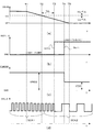
===USBケーブルを取り外した場合の動作===
図3を用いて、音楽ファイルのデータ転送が完了したことや突発的な事故等に伴って、USBインタフェース101にUSBケーブル400が接続された状況から、USBケーブル400が取り外された状況へと切り替えた場合におけるASIC200の動作について説明する。なお、図3(a)は、VBUS端子206に印加される電圧レベルの波形を示し、図3(b)は、電源電圧監視部270より出力される選択信号DET1、2の波形を示し、図3(c)は、VDD端子208へと印加される電源電圧の波形を示し、図3(d)は、クロック選択部290からマイクロコンピュータ210へと供給されるクロックの波形を示した図である。
<Operation of ASIC>
=== Operation when USB cable is removed ===
Using FIG. 3, switching from the state in which the
まず、USBインタフェース101にUSBケーブル400が接続され、パーソナルコンピュータ300から携帯オーディオ再生機器100に向けて音楽ファイルのデータ転送並びに電源電圧VBUSの供給がなされている場合とする。
First, it is assumed that the
従って、VBUS端子206に印加される電圧レベルは「5V」であり(図3(a)参照)、電源電圧監視部270においてパーソナルコンピュータ300から電源電圧VBUSが供給されている旨(DET1、DET2が共にLowレベル)が判定される(図3(b)参照)。この結果、電源電圧選択部105ではLowレベルの選択信号DET1に基づいてレギュレート電源電圧VREGが選択され(図3(c)参照)、また、クロック選択部290ではLowレベルの選択信号DET2に基づいて逓倍クロックSCK1が選択される。
Therefore, the voltage level applied to the
時刻T1では、USBインタフェース101からUSBケーブル400が取り外される。この場合、時刻T1から時刻T5に向けて、VBUS端子206へと印加される電圧レベルは、電源ライン102に接続されたプルダウン抵抗Rdに基づいて「0V」へと徐々に減衰していく(図3(a)参照)。
At time T1, the
つぎに、時刻T2では、二値化処理部271の出力は、VBUS端子206へと印加された電圧レベルが参照レベルVthを下回る(図3(a)参照)。しかし、スパイク状の電源ノイズによる誤判定を防ぐために、判定処理部272より出力される選択信号DET1、DET2は、Lowレベルのままである(図3(b)参照)。
Next, at time T2, the output of the
つぎに、時刻T2から一定期間Tth経過した時刻T3では、まず、選択信号DET2を選択信号DET1より先にLowレベルからHighレベルへと切り替える(図3(b)参照)。この理由は、二値化処理部271の出力はLowレベルを継続しているので、判定処理部272は、電源ノイズに起因したレベル変化とは見なさないためである。この結果、クロック選択部290ではHighレベルの選択信号DET2に基づいて原クロックSCK2が選択される(図3(d)参照)。
Next, at time T3 when a certain period Tth has elapsed from time T2, first, the selection signal DET2 is switched from the Low level to the High level before the selection signal DET1 (see FIG. 3B). This is because the output of the
つぎに、時刻T5においてVBUS端子206の電圧レベルが「0V」へと完全に減衰する前の時刻T4では、判定処理部272は、選択信号DET1をLowレベルからHighレベルへと切り替える。この結果、電源電圧選択部105ではHighレベルの選択信号DET1に基づいて電源電圧VDDが選択される(図3(c)参照)。
Next, at time T4 before the voltage level of the
このように、クロック選択部290は、電源電圧監視部270において、パーソナルコンピュータ300から電源電圧VBUSが供給されている旨の判定から、パーソナルコンピュータ300から電源電圧VBUSが供給されていない旨の判定へと切り替わる場合、電源電圧選択部105においてレギュレート電源電圧VREGの選択から電源電圧VDDの選択へと切り替えられるよりも先に、逓倍クロックSCK1の選択から原クロックSCK2の選択へと切り替える。
As described above, the
すなわち、逓倍クロックSCK1の使用は、あくまで、レギュレート電源電圧VREGの供給が前提条件である。このため、USBケーブル400の取り外しに伴って、高周波数の逓倍クロックSCK1から低周波数の原クロックSCK2へと切り替えた上で、高レベルのレギュレート電源電圧VREGから低レベルの電源電圧VDDへと切り替える。
That is, the use of the multiplied clock SCK1 is based on the precondition that the regulated power supply voltage VREG is supplied. Therefore, when the
===USBケーブルを接続した場合の動作===
図4を用いて、音楽ファイルのデータ転送を行うべく、USBインタフェース101からUSBケーブル400が取り外された状況から、USBインタフェース101にUSBケーブル400を接続した状況へと切り替えた場合におけるASIC200の動作について説明する。なお、図4(a)乃至(d)は、図3(a)乃至(d)それぞれと同様の波形を示した図である。
=== Operation when USB cable is connected ===
Referring to FIG. 4, the operation of the
まず、USBインタフェース101からUSBケーブル400が取り外されており、携帯オーディオ再生機器100はパーソナルコンピュータ300から電源電圧VBUSの供給を受けていない場合とする。
First, it is assumed that the
従って、VBUS端子206に印加される電圧レベルは「0V」であり(図4(a)参照)、電源電圧監視部270においてパーソナルコンピュータ300から電源電圧VBUSが供給されていない旨(DET1、DET2が共にHighレベル)が判定される(図4(b)参照)。この結果、電源電圧選択部105ではHighレベルの選択信号DET1に基づいて電源電圧VDDの方が選択され(図4(c)参照)、また、クロック選択部290ではHighレベルの選択信号DET2に基づいて原クロックSCK2の方が選択される。
Therefore, the voltage level applied to the
時刻T1では、USBインタフェース101にUSBケーブル400を接続する。この場合、時刻T1から時刻T5に向けて、VBUS端子206へと印加される電圧レベルは、「0V」から「5V」へと徐々に上昇していく(図4(a)参照)。
At time T1, the
つぎに、時刻T2では、二値化処理部271の出力は、VBUS端子206へと印加された電圧レベルが参照レベルVthを上回る(図4(a)参照)。しかし、スパイク状の電源ノイズによる誤判定を防ぐために、判定処理部272から出力される選択信号DET1、DET2は、Highレベルのままである(図4(b)参照)。
Next, at time T2, the output of the
つぎに、時刻T2から一定期間Tth経過した時刻T3では、まず、選択信号DET1を選択信号DET2より先にHighレベルからLowレベルへと切り替える(図4(b)参照)。この理由は、二値化処理部271の出力はHighレベルを継続しているので、判定処理部272は、電源ノイズに起因したレベル変化とは見なさないためである。なお、時刻T1から時刻T3までの期間中では、レギュレート回路103によってレギュレート電源電圧VREGが生成されている。この結果、電源電圧選択部105ではLowレベルの選択信号DET1に基づいてレギュレート電源電圧VREGが選択される(図4(c)参照)。
Next, at time T3 when a predetermined period Tth has elapsed from time T2, first, the selection signal DET1 is switched from the high level to the low level before the selection signal DET2 (see FIG. 4B). This is because, since the output of the
つぎに、時刻T5においてVBUS端子206の電圧レベルが「5V」へと完全に上昇する前の時刻T4では、判定処理部272は、選択信号DET2をHighレベルからLowレベルへと切り替える。この結果、クロック選択部290ではLowレベルの選択信号DET2に基づいて逓倍クロックSCK1が選択される(図4(d)参照)。
Next, at time T4 before the voltage level of the
このように、クロック選択部290は、電源電圧監視部270において、パーソナルコンピュータ300から電源電圧VBUSが供給されていない旨の判定から、パーソナルコンピュータ300から電源電圧VBUSが供給されている旨の判定へと切り替わった場合、電源電圧選択部105において電源電圧VDDの選択からレギュレート電源電圧VREGの選択へと切り替えられるよりも後に、原クロックSCK2の選択から逓倍クロックSCK1の選択へと切り替える。
As described above, the
すなわち、逓倍クロックSCK1の使用は、あくまで、レギュレート電源電圧VREGの供給が前提条件である。このため、USBケーブル400を接続したことに伴って、低レベルの電源電圧VDDから高レベルのレギュレート電源電圧VREGへと切り替えた上で、低周波数の原クロックSCK2から高周波数の逓倍クロックSCK1へと切り替える。
That is, the use of the multiplied clock SCK1 is based on the precondition that the regulated power supply voltage VREG is supplied. Therefore, when the
以上、本発明の実施形態について説明したが、前述した実施形態は、本発明の理解を容易にするためのものであり、本発明を限定して解釈するためのものではない。本発明は、その趣旨を逸脱することなく、変更/改良され得るとともに、その等価物も含まれる。 As mentioned above, although embodiment of this invention was described, embodiment mentioned above is for making an understanding of this invention easy, and is not for limiting and interpreting this invention. The present invention can be changed / improved without departing from the gist thereof, and equivalents thereof are also included.
100 携帯オーディオ再生機器 101、320 USBインタフェース
102、402 電源ライン 103 レギュレート回路
104 内部電源 105 電源電圧選択部
106 不揮発性メモリ 107 水晶発振器
200 ASIC 201 D+端子
202 D−端子 203 MI端子
204 OUT端子 205 XTAL端子
206 VBUS端子 207 DET端子
208 VDD端子 210 マイクロコンピュータ
220、310 USBコントローラ 230 メモリインタフェース回路
240 DSP 250 RAM
260 DA変換器 270 電源電圧監視部
271 二値化処理部 272 判定処理部
280 PLL回路 290 クロック選択部
300 パーソナルコンピュータ 330 CPU
340 メモリ 350 ハードディスク
360 電源アダプタ 361 電源プラグ
400 USBケーブル 401 データライン
403 GNDライン
DESCRIPTION OF
260
340
Claims (7)
前記外部電源から供給される前記第1の電源電圧のレベルを監視して前記外部電源から前記第1の電源電圧が供給されているか否かを判定する電源電圧監視部と、
第1の周波数の第1のクロック及び前記第1の周波数よりも低い第2の周波数を有する第2のクロックが供給され、前記電源電圧監視部において、前記第1の電源電圧が供給されている旨が判定された場合には前記第1のクロックを選択し、前記第1の電源電圧が供給されていない旨が判定された場合には前記第2のクロックを選択し出力するクロック選択部と、
前記クロック選択部が出力する前記第1のクロック又は前記第2のクロックのうちいずれか一方の供給を受けて動作し、前記集積回路の動作を制御するプロセッサと、
を備え、
当該集積回路は、前記外部電源、又は、前記第1の電源電圧よりもレベルの低い第2の電源電圧を供給する内部電源、のうちいずれか一方が印加されて動作するものであって、
前記電源電圧監視部は、前記第1の電源電圧が供給されている旨が判定された場合には前記第1の電源電圧が印加され、前記第1の電源電圧が供給されていない旨が判定された場合には前記第2の電源電圧が印加されるべく制御を行うこと、
を特徴とする集積回路。 In an integrated circuit that operates by applying an external power supply for supplying a first power supply voltage,
A power supply voltage monitoring unit that monitors a level of the first power supply voltage supplied from the external power supply and determines whether or not the first power supply voltage is supplied from the external power supply;
A first clock having a first frequency and a second clock having a second frequency lower than the first frequency are supplied, and the power supply voltage monitoring unit supplies the first power supply voltage. A clock selection unit that selects the first clock when it is determined, and selects and outputs the second clock when it is determined that the first power supply voltage is not supplied. ,
A processor that operates by receiving one of the first clock and the second clock output from the clock selector and controls the operation of the integrated circuit;
Equipped with a,
The integrated circuit operates by applying either the external power supply or an internal power supply that supplies a second power supply voltage having a level lower than the first power supply voltage,
When it is determined that the first power supply voltage is supplied, the power supply voltage monitoring unit determines that the first power supply voltage is applied and the first power supply voltage is not supplied. If so, control to apply the second power supply voltage;
An integrated circuit characterized by.
前記第2のクロックに基づいて前記第1のクロックを生成するPLL回路を備えること、を特徴とする集積回路。 The integrated circuit of claim 1, wherein the integrated circuit further comprises:
An integrated circuit comprising: a PLL circuit that generates the first clock based on the second clock.
前記第1の電源電圧の供給開始の際には電源電圧の変化の後に前記クロック選択部における選択を切り替え、前記第1の電源電圧の供給終了の際には電源電圧の変化に先立って前記クロック選択部における選択を切り替えること、を特徴とする集積回路。 The integrated circuit according to claim 1 , wherein the power supply voltage monitoring unit includes:
When the supply of the first power supply voltage starts, the selection in the clock selection unit is switched after the change of the power supply voltage, and when the supply of the first power supply voltage ends, the clock is changed prior to the change of the power supply voltage. An integrated circuit characterized by switching selection in a selection unit.
デジタルデータをデコード処理するデジタル信号処理回路を備え、当該デジタル信号処理回路は、前記電源電圧監視部が選択制御する前記第1の電源電圧又は前記第2の電源電圧のうちいずれか一方に応じて動作すること、を特徴とする集積回路。 The integrated circuit according to claim 1 or 3 , further comprising:
A digital signal processing circuit for decoding digital data, the digital signal processing circuit corresponding to one of the first power supply voltage and the second power supply voltage selected and controlled by the power supply voltage monitoring unit; An integrated circuit characterized by operating.
前記外部電源及び前記内部電源に接続され、前記電源電圧監視部の判定結果に応じて前記第1の電源電圧又は前記第2の電源電圧のうちいずれか一方を出力する電源電圧選択部を備え、
前記集積回路は、前記電源電圧選択部が出力する前記第1の電源電圧又は前記第2の電源電圧のうちいずれか一方に応じて動作すること、を特徴とする集積回路。 The signal processing apparatus comprising the integrated circuit according to claim 5 , further comprising:
A power supply voltage selection unit that is connected to the external power supply and the internal power supply and outputs either the first power supply voltage or the second power supply voltage according to a determination result of the power supply voltage monitoring unit;
The integrated circuit operates in accordance with either the first power supply voltage or the second power supply voltage output from the power supply voltage selection unit.
前記デジタルデータを格納する不揮発性メモリを備え、
前記デジタル信号処理回路は、前記不揮発性メモリに格納された前記デジタルデータを読み出してデコード処理を行うこと、を特徴とする信号処理装置。 The signal processing device according to claim 6 , further comprising:
Comprising a non-volatile memory for storing the digital data;
The signal processing apparatus, wherein the digital signal processing circuit reads out the digital data stored in the nonvolatile memory and performs a decoding process.
Priority Applications (5)
| Application Number | Priority Date | Filing Date | Title |
|---|---|---|---|
| JP2006080796A JP4669803B2 (en) | 2006-03-23 | 2006-03-23 | Integrated circuit and signal processing apparatus using the same |
| CN2007100857448A CN101042610B (en) | 2006-03-23 | 2007-03-08 | Integrated circuit and signal processing apparatus using the same |
| US11/688,599 US7664973B2 (en) | 2006-03-23 | 2007-03-20 | Integrated circuit and signal processing apparatus using the same |
| KR1020070027971A KR100972271B1 (en) | 2006-03-23 | 2007-03-22 | Integrated circuit and signal processing device using the same |
| TW096109855A TW200809485A (en) | 2006-03-23 | 2007-03-22 | Integrated circuit and signal prosessing device using the same |
Applications Claiming Priority (1)
| Application Number | Priority Date | Filing Date | Title |
|---|---|---|---|
| JP2006080796A JP4669803B2 (en) | 2006-03-23 | 2006-03-23 | Integrated circuit and signal processing apparatus using the same |
Publications (3)
| Publication Number | Publication Date |
|---|---|
| JP2007257290A JP2007257290A (en) | 2007-10-04 |
| JP2007257290A5 JP2007257290A5 (en) | 2010-01-14 |
| JP4669803B2 true JP4669803B2 (en) | 2011-04-13 |
Family
ID=38557925
Family Applications (1)
| Application Number | Title | Priority Date | Filing Date |
|---|---|---|---|
| JP2006080796A Expired - Fee Related JP4669803B2 (en) | 2006-03-23 | 2006-03-23 | Integrated circuit and signal processing apparatus using the same |
Country Status (5)
| Country | Link |
|---|---|
| US (1) | US7664973B2 (en) |
| JP (1) | JP4669803B2 (en) |
| KR (1) | KR100972271B1 (en) |
| CN (1) | CN101042610B (en) |
| TW (1) | TW200809485A (en) |
Families Citing this family (9)
| Publication number | Priority date | Publication date | Assignee | Title |
|---|---|---|---|---|
| US20120066536A1 (en) * | 2009-06-25 | 2012-03-15 | Ronnie Gozun | Systems And Methods For Delivering Power |
| TWI428750B (en) * | 2010-12-30 | 2014-03-01 | Via Tech Inc | Processing device and operation system utilizing the same |
| JP2012163446A (en) * | 2011-02-07 | 2012-08-30 | Kawamura Electric Inc | Current measuring device |
| US9037892B2 (en) | 2011-04-13 | 2015-05-19 | International Business Machines Corporation | System-wide power management control via clock distribution network |
| US8724281B2 (en) | 2012-04-25 | 2014-05-13 | Apple Inc. | Techniques for detecting removal of a connector |
| US8891216B2 (en) | 2012-04-25 | 2014-11-18 | Apple Inc. | Techniques for detecting removal of a connector |
| US9032117B2 (en) * | 2013-07-10 | 2015-05-12 | Cisco Technology, Inc. | Active cable with display |
| CN104007977A (en) * | 2014-06-09 | 2014-08-27 | 威盛电子股份有限公司 | Electronic device and audio playing method |
| KR102576430B1 (en) * | 2016-11-18 | 2023-09-08 | 삼성전자주식회사 | Apparatus for providing interface |
Citations (2)
| Publication number | Priority date | Publication date | Assignee | Title |
|---|---|---|---|---|
| JP2003256073A (en) * | 2002-03-04 | 2003-09-10 | Sony Corp | Information processor and method and program |
| JP2004070805A (en) * | 2002-08-08 | 2004-03-04 | Fujitsu Ltd | Semiconductor integrated circuit with controlled internal power source voltage |
Family Cites Families (14)
| Publication number | Priority date | Publication date | Assignee | Title |
|---|---|---|---|---|
| JPH0497408A (en) * | 1990-08-15 | 1992-03-30 | Fujitsu Ltd | Portable information processor |
| US5524249A (en) * | 1994-01-27 | 1996-06-04 | Compaq Computer Corporation | Video subsystem power management apparatus and method |
| US5991883A (en) * | 1996-06-03 | 1999-11-23 | Compaq Computer Corporation | Power conservation method for a portable computer with LCD display |
| US6178514B1 (en) * | 1998-07-31 | 2001-01-23 | Bradley C. Wood | Method and apparatus for connecting a device to a bus carrying power and a signal |
| JP2000122756A (en) * | 1998-10-19 | 2000-04-28 | Fujitsu Ltd | Electronic equipment |
| JP3819658B2 (en) | 1999-12-27 | 2006-09-13 | 三洋電機株式会社 | Portable electronic devices with a common serial bus connector |
| JP2001184147A (en) * | 1999-12-27 | 2001-07-06 | Sanyo Electric Co Ltd | Portable electronic equipment |
| US6631474B1 (en) * | 1999-12-31 | 2003-10-07 | Intel Corporation | System to coordinate switching between first and second processors and to coordinate cache coherency between first and second processors during switching |
| JP2003029885A (en) | 2001-07-17 | 2003-01-31 | Sony Corp | Power supply system and electronic equipment |
| JP3842609B2 (en) * | 2001-10-22 | 2006-11-08 | 株式会社東芝 | IC card LSI, IC card, and IC card operation method |
| US7076674B2 (en) * | 2001-12-19 | 2006-07-11 | Hewlett-Packard Development Company L.P. | Portable computer having dual clock mode |
| US7013396B2 (en) * | 2002-09-26 | 2006-03-14 | Intel Corporation | Circuit for enabling dual mode safe power-on sequencing |
| JP2005250943A (en) | 2004-03-05 | 2005-09-15 | Fujitsu Ltd | External connection equipment and processor capable of being supplied with power via interface means |
| JP5016783B2 (en) | 2004-08-11 | 2012-09-05 | 株式会社東芝 | Information processing apparatus and power supply control method thereof |
-
2006
- 2006-03-23 JP JP2006080796A patent/JP4669803B2/en not_active Expired - Fee Related
-
2007
- 2007-03-08 CN CN2007100857448A patent/CN101042610B/en not_active Expired - Fee Related
- 2007-03-20 US US11/688,599 patent/US7664973B2/en active Active
- 2007-03-22 TW TW096109855A patent/TW200809485A/en not_active IP Right Cessation
- 2007-03-22 KR KR1020070027971A patent/KR100972271B1/en not_active IP Right Cessation
Patent Citations (2)
| Publication number | Priority date | Publication date | Assignee | Title |
|---|---|---|---|---|
| JP2003256073A (en) * | 2002-03-04 | 2003-09-10 | Sony Corp | Information processor and method and program |
| JP2004070805A (en) * | 2002-08-08 | 2004-03-04 | Fujitsu Ltd | Semiconductor integrated circuit with controlled internal power source voltage |
Also Published As
| Publication number | Publication date |
|---|---|
| TW200809485A (en) | 2008-02-16 |
| KR100972271B1 (en) | 2010-07-23 |
| US7664973B2 (en) | 2010-02-16 |
| CN101042610B (en) | 2010-04-21 |
| TWI338833B (en) | 2011-03-11 |
| CN101042610A (en) | 2007-09-26 |
| KR20070096844A (en) | 2007-10-02 |
| JP2007257290A (en) | 2007-10-04 |
| US20070229122A1 (en) | 2007-10-04 |
Similar Documents
| Publication | Publication Date | Title |
|---|---|---|
| JP5385500B2 (en) | Signal processing device | |
| JP4669803B2 (en) | Integrated circuit and signal processing apparatus using the same | |
| JP5547372B2 (en) | Apparatus and method for enabling digital and analog data communication over a data bus | |
| JP4601330B2 (en) | Electronic device and control method thereof, information processing apparatus, and computer program | |
| KR102468187B1 (en) | Eletronic device and external device charging method thereof | |
| US6774604B2 (en) | Power control circuit, electronic instrument, and charging method | |
| US7882383B2 (en) | System on a chip with RTC power supply | |
| KR101729511B1 (en) | Computer system and control method thereof | |
| US9990027B2 (en) | Status switching method | |
| JP2013101520A (en) | Peripheral device and its power supply control method | |
| JP2004110762A (en) | Large capacity storage loading body of radio communication | |
| JP2007102370A (en) | Electronic device, method for controlling operation mode executed thereby, and electronic device system | |
| JP4050924B2 (en) | Data processing device | |
| JP2013196179A (en) | Charge control device and electronic apparatus | |
| JP2004302778A (en) | Interface device | |
| JP2023040804A (en) | Port controller and electronic apparatus | |
| JP2011022669A (en) | Image forming apparatus and information processing system | |
| KR200330771Y1 (en) | Cable for data communication | |
| TW201626250A (en) | Electronic device with multiple interfaces | |
| US20070041122A1 (en) | Communication method and system | |
| US9740273B2 (en) | File sharing circuit and computer using the same | |
| JP3099746U (en) | Digital data transfer device | |
| CN114204652A (en) | Power supply device and control method thereof | |
| JP2010060713A (en) | Integrated circuit device and sound reproduction system | |
| JP2010176408A (en) | Controller and controlled device |
Legal Events
| Date | Code | Title | Description |
|---|---|---|---|
| A621 | Written request for application examination |
Free format text: JAPANESE INTERMEDIATE CODE: A621 Effective date: 20090227 |
|
| A521 | Written amendment |
Free format text: JAPANESE INTERMEDIATE CODE: A523 Effective date: 20091120 |
|
| TRDD | Decision of grant or rejection written | ||
| A01 | Written decision to grant a patent or to grant a registration (utility model) |
Free format text: JAPANESE INTERMEDIATE CODE: A01 Effective date: 20101221 |
|
| A01 | Written decision to grant a patent or to grant a registration (utility model) |
Free format text: JAPANESE INTERMEDIATE CODE: A01 |
|
| A61 | First payment of annual fees (during grant procedure) |
Free format text: JAPANESE INTERMEDIATE CODE: A61 Effective date: 20110117 |
|
| FPAY | Renewal fee payment (event date is renewal date of database) |
Free format text: PAYMENT UNTIL: 20140121 Year of fee payment: 3 |
|
| R150 | Certificate of patent or registration of utility model |
Free format text: JAPANESE INTERMEDIATE CODE: R150 |
|
| FPAY | Renewal fee payment (event date is renewal date of database) |
Free format text: PAYMENT UNTIL: 20140121 Year of fee payment: 3 |
|
| S111 | Request for change of ownership or part of ownership |
Free format text: JAPANESE INTERMEDIATE CODE: R313113 |
|
| FPAY | Renewal fee payment (event date is renewal date of database) |
Free format text: PAYMENT UNTIL: 20140121 Year of fee payment: 3 |
|
| R350 | Written notification of registration of transfer |
Free format text: JAPANESE INTERMEDIATE CODE: R350 |
|
| FPAY | Renewal fee payment (event date is renewal date of database) |
Free format text: PAYMENT UNTIL: 20140121 Year of fee payment: 3 |
|
| S111 | Request for change of ownership or part of ownership |
Free format text: JAPANESE INTERMEDIATE CODE: R313113 |
|
| FPAY | Renewal fee payment (event date is renewal date of database) |
Free format text: PAYMENT UNTIL: 20140121 Year of fee payment: 3 |
|
| R350 | Written notification of registration of transfer |
Free format text: JAPANESE INTERMEDIATE CODE: R350 |
|
| R250 | Receipt of annual fees |
Free format text: JAPANESE INTERMEDIATE CODE: R250 |
|
| LAPS | Cancellation because of no payment of annual fees |