JP4667587B2 - Liquid crystal display device - Google Patents
Liquid crystal display device Download PDFInfo
- Publication number
- JP4667587B2 JP4667587B2 JP2000367769A JP2000367769A JP4667587B2 JP 4667587 B2 JP4667587 B2 JP 4667587B2 JP 2000367769 A JP2000367769 A JP 2000367769A JP 2000367769 A JP2000367769 A JP 2000367769A JP 4667587 B2 JP4667587 B2 JP 4667587B2
- Authority
- JP
- Japan
- Prior art keywords
- signal line
- liquid crystal
- reference electrode
- drain
- pixel
- Prior art date
- Legal status (The legal status is an assumption and is not a legal conclusion. Google has not performed a legal analysis and makes no representation as to the accuracy of the status listed.)
- Expired - Lifetime
Links
Images


Classifications
-
- G—PHYSICS
- G02—OPTICS
- G02F—OPTICAL DEVICES OR ARRANGEMENTS FOR THE CONTROL OF LIGHT BY MODIFICATION OF THE OPTICAL PROPERTIES OF THE MEDIA OF THE ELEMENTS INVOLVED THEREIN; NON-LINEAR OPTICS; FREQUENCY-CHANGING OF LIGHT; OPTICAL LOGIC ELEMENTS; OPTICAL ANALOGUE/DIGITAL CONVERTERS
- G02F1/00—Devices or arrangements for the control of the intensity, colour, phase, polarisation or direction of light arriving from an independent light source, e.g. switching, gating or modulating; Non-linear optics
- G02F1/01—Devices or arrangements for the control of the intensity, colour, phase, polarisation or direction of light arriving from an independent light source, e.g. switching, gating or modulating; Non-linear optics for the control of the intensity, phase, polarisation or colour
- G02F1/13—Devices or arrangements for the control of the intensity, colour, phase, polarisation or direction of light arriving from an independent light source, e.g. switching, gating or modulating; Non-linear optics for the control of the intensity, phase, polarisation or colour based on liquid crystals, e.g. single liquid crystal display cells
- G02F1/133—Constructional arrangements; Operation of liquid crystal cells; Circuit arrangements
- G02F1/1333—Constructional arrangements; Manufacturing methods
- G02F1/1343—Electrodes
- G02F1/134309—Electrodes characterised by their geometrical arrangement
- G02F1/134363—Electrodes characterised by their geometrical arrangement for applying an electric field parallel to the substrate, i.e. in-plane switching [IPS]
-
- G—PHYSICS
- G09—EDUCATION; CRYPTOGRAPHY; DISPLAY; ADVERTISING; SEALS
- G09G—ARRANGEMENTS OR CIRCUITS FOR CONTROL OF INDICATING DEVICES USING STATIC MEANS TO PRESENT VARIABLE INFORMATION
- G09G3/00—Control arrangements or circuits, of interest only in connection with visual indicators other than cathode-ray tubes
- G09G3/20—Control arrangements or circuits, of interest only in connection with visual indicators other than cathode-ray tubes for presentation of an assembly of a number of characters, e.g. a page, by composing the assembly by combination of individual elements arranged in a matrix no fixed position being assigned to or needed to be assigned to the individual characters or partial characters
- G09G3/34—Control arrangements or circuits, of interest only in connection with visual indicators other than cathode-ray tubes for presentation of an assembly of a number of characters, e.g. a page, by composing the assembly by combination of individual elements arranged in a matrix no fixed position being assigned to or needed to be assigned to the individual characters or partial characters by control of light from an independent source
- G09G3/36—Control arrangements or circuits, of interest only in connection with visual indicators other than cathode-ray tubes for presentation of an assembly of a number of characters, e.g. a page, by composing the assembly by combination of individual elements arranged in a matrix no fixed position being assigned to or needed to be assigned to the individual characters or partial characters by control of light from an independent source using liquid crystals
- G09G3/3611—Control of matrices with row and column drivers
- G09G3/3648—Control of matrices with row and column drivers using an active matrix
-
- G—PHYSICS
- G02—OPTICS
- G02F—OPTICAL DEVICES OR ARRANGEMENTS FOR THE CONTROL OF LIGHT BY MODIFICATION OF THE OPTICAL PROPERTIES OF THE MEDIA OF THE ELEMENTS INVOLVED THEREIN; NON-LINEAR OPTICS; FREQUENCY-CHANGING OF LIGHT; OPTICAL LOGIC ELEMENTS; OPTICAL ANALOGUE/DIGITAL CONVERTERS
- G02F1/00—Devices or arrangements for the control of the intensity, colour, phase, polarisation or direction of light arriving from an independent light source, e.g. switching, gating or modulating; Non-linear optics
- G02F1/01—Devices or arrangements for the control of the intensity, colour, phase, polarisation or direction of light arriving from an independent light source, e.g. switching, gating or modulating; Non-linear optics for the control of the intensity, phase, polarisation or colour
- G02F1/13—Devices or arrangements for the control of the intensity, colour, phase, polarisation or direction of light arriving from an independent light source, e.g. switching, gating or modulating; Non-linear optics for the control of the intensity, phase, polarisation or colour based on liquid crystals, e.g. single liquid crystal display cells
- G02F1/133—Constructional arrangements; Operation of liquid crystal cells; Circuit arrangements
- G02F1/1333—Constructional arrangements; Manufacturing methods
- G02F1/1345—Conductors connecting electrodes to cell terminals
- G02F1/13452—Conductors connecting driver circuitry and terminals of panels
Landscapes
- Physics & Mathematics (AREA)
- Nonlinear Science (AREA)
- Chemical & Material Sciences (AREA)
- Crystallography & Structural Chemistry (AREA)
- General Physics & Mathematics (AREA)
- Engineering & Computer Science (AREA)
- Mathematical Physics (AREA)
- Optics & Photonics (AREA)
- Geometry (AREA)
- Computer Hardware Design (AREA)
- Theoretical Computer Science (AREA)
- Liquid Crystal (AREA)
Abstract
Description
【0001】
【発明の属する技術分野】
本発明は液晶表示装置に係り、特に、アクティブ・マトリクス型の液晶表示装置に関する。
【0002】
【従来の技術】
アクティブ・マトリクス型の液晶表示装置は、液晶を介して対向配置される各基板のうち一方の基板の液晶側の面に、x方向に延在しy方向に並設されるゲート信号線とy方向に延在しx方向に並設されるドレイン信号線とで囲まれる各領域を画素領域とし、この画素領域にはゲート信号線からの走査信号によって作動するアクティブ素子と、このアクティブ素子を介してドレイン信号線からの映像信号が供給される画素電極と、この画素電極との間に生じせしめる容量を備えている。
【0003】
このような液晶表示装置は、アクティブ素子により一定時間の書き込みと一定時間の保持を行って画素表示を実現している。
【0004】
この保持方式として、ゲート信号線と画素電極の間で容量を形成するCadd(付加容量)方式と、保持容量信号線と画素電極の間で容量を形成するCstg(保持容量)方式とが知られている。
【0005】
Cstg方式は保持容量信号線が必要なために開口率が低下するが、保持電位を安定にできるため、比較的高画質を得ることができる。
【0006】
また、Cstg方式を用いた液晶表示装置として、いわゆる横電界方式と称されるのが知られている。この種の液晶表示装置は、画素電極が形成された基板側に該画素電極との間に電界を生じせしめる基準電極が設けられて構成され、この基準電極に基準信号を供給する基準信号線に絶縁膜を介して画素電極を重畳させることによって保持容量を形成している。
【0007】
これは、液晶表示装置の表示の広視野角化を実現できるものとして、近年、この方式を用いたものが製品化されている。
【0008】
一方、液晶を介して対向配置される各基板の間隙(セルギャップ)を均一に確保するため、該液晶内にポリマー静ビーズを分散する構成、あるいは一方の基板面にホトリソグラフィ技術による選択エッチングにより有機材料の支柱を設ける構成が知られている。
【0009】
ビーズあるいは支柱の周辺では光漏れが生じるが、画面内に支柱を配置する手法では予めその位置を設定できるため、ビーズ分散による手法よりもコントラスト比の向上を実現できる。
【0010】
また、アクティブ素子に信号を供給するドライバ(半導体チップ)の実装として、TCP方式とFCA(COGとも称す)方式とが知られている。
【0011】
TCP方式は、FCP方式よりも容易に製造でき、歩留まりが向上できるという特徴を有する。また、FCP方式は外部への引き出し配線の本数を低減できるため、高精細化に適する。
【0012】
【発明が解決しようとする課題】
(課題1)
まず、広視野角かつ高精細度の液晶表示装置を実現するためには、前述の横電界方式にFCA方式を採用することが望ましい。
【0013】
しかし、横電界方式は、その液晶の表示モードは複屈折モードであるため、たとえばTNモードと比べると液晶層の厚みの変動に対して敏感となり、同じ液晶層厚の変動量に対しより着色して見えるという不都合が有する。
【0014】
また、FCA方式は、そのドライバが直接に液晶表示装置の基板に搭載されるため、該ドライバからの発熱が液晶表示装置の基板に直接伝わり、該ドライバの近傍の液晶に局所的な温度上昇を招き、この部分に変色して見えるという不都合が生じることを見出した。
(課題2)
また、FCA方式を採用した場合、半導体チップのみからなるドライバをそのまま液晶表示装置の基板に実装する場合が多く、該半導体チップの周辺の基板に応力が生じ易くなる。
【0015】
そして、この応力のために、表示面のドライバの近傍の部分に変色して見える不都合が生じることを見出した。
【0016】
この場合、いわゆるノーマリブラックモードの場合、黒表示時に光抜けが生じ、コントラスト比の低下にまで到ることを確認した。ここで、ノーマリブラックモードとは液晶に電界を印加していない状態で該液晶の光透過率は最低となるように構成された態様をいう。
(課題3)
また、液晶を介して対向配置させる各基板のギャップを均一にするため、片側の基板に支柱を形成する場合、上記課題2で示した応力が原因して、チップ近傍の領域で上下基板の併せずれが他の領域より悪化するということが判明した。
【0017】
ビーズを用いた場合、その形状が球体でありかつ強固な固定はされていないことにより、局所的な応力が加わった場合、それを緩和する方向にビーズの再配置がおこり、結果として半導体チップの近傍の上下基板の合わせずれが低減する。
【0018】
しかし、支柱の場合、支柱と基板が面接触であり接触面積が大きいため、また、支柱自体は片側の基板に固定されているため、応力による半導体チップ近傍の局所的アライメントずれがそのままとなり、緩和されることがない。
(課題4)
さらに、横電界方式の場合、互いに電界を発生せしめる画素電極と基準電極のうち、基準電極は映像信号線に隣接した配置させることが知られている。
【0019】
映像信号線からの電界を基準電極側に終端させて画素電極側にまで影響させないようにするためである。
【0020】
そして、映像信号線と基準電極との間には間隙が形成され、この間隙部において液晶が駆動しいわゆるドメインの発生が生じるため、この部分に遮光膜を形成することが行われている。
【0021】
しかし、該遮光膜の形成は画素の開口率を向上を妨げるということが指摘されている。
(課題5)
さらに、ゲート信号線あるいはドレンイ信号線のドライバとの接続にあって、該ドライバの近傍の信号線は半導体チップの寸法にまで絞り込むパターンとして形成されている。
【0022】
この場合において、上記以外の信号線たとえば基準信号線をも半導体チップ側に引出し、上記各信号線の絞り込まれた部分で別の配線層に接続させることが必要とされ、このためのコンタクト領域の確保が要求される。
【0023】
しかし、そのための領域の確保からいわゆる額縁(基板の外輪郭から表示面までの幅で形成される部分)の縮小を確保できない不都合が生じる。
【0024】
本発明は、上記課題1に示した不都合を解消するため、すなわち、ドライバ近傍の液晶の局所的温度上昇を抑制させた液晶表示装置を提供することにある。
【0025】
本発明は、上記課題2に示した不都合を解消するため、すなわち、ドライバの基板に対する応力の伝達を抑制させた液晶表示装置を提供することにある。
【0026】
本発明は、上記課題3に示した不都合を解消するため、すなわち、ドライバ近傍の表示面にてアライメントずれを抑制させた液晶表示装置を提供することにある。
【0027】
本発明は、上記課題4に示した不都合を解消するため、すなわち、開口率を向上せた液晶表示装置を提供することにある。
【0028】
本発明は、上記課題5に示した不都合を解消するため、すなわち、いわゆる額縁の縮小を図った液晶表示装置を提供することにある。
【0029】
【課題を解決するための手段】
本発明において開示される発明のうち、代表的なものの概要を簡単に説明すれば、以下のとおりである。
【0030】
上記課題1を解決するための代表的な手段としては、たとえば、液晶層を介して対向配置される各基板のうち一方の基板の液晶側の面にて、
その各画素領域に、ゲート信号線からの走査信号によって作動されるスイッチング素子と、このスイッチング素子を介してドレイン信号線からの映像信号が供給される画素電極と、この画素電極との間に電界を生じせしめる基準電極とを備えるとともに、
前記ドレイン信号線からの映像信号は前記一方の基板上に実装されたドライバチップによってなされ、
画素電極と基準電極との間の電圧が印加されていない場合に前記液晶層の光透過率が最低になるように構成されているとともに、
前記映像信号の電圧最大振幅を前記液晶層の相対透過率を90%とするのに要する電圧以下に設定されていることを特徴とするものである。
【0031】
上記課題2を解決するための代表的な手段としては、たとえば、液晶層を介して対向配置される各基板のうち一方の基板の液晶側の面にて、
その各画素領域に、ゲート信号線からの走査信号によって作動されるスイッチング素子と、このスイッチング素子を介してドレイン信号線からの映像信号が供給される画素電極と、この画素電極との間に電界を生じせしめる基準電極とを備えるとともに、
前記ドレイン信号線からの映像信号は前記一方の基板上に実装されたドライバチップによってなされ、
該ドライバチップの前記一方の基板との間に応力緩衝層が介在されていることを特徴とするものである。
【0032】
上記課題3を解決するための代表的な手段としては、たとえば、液晶層を介して対向配置される各基板のうち一方の基板の液晶側の面にて、
その各画素領域に、ゲート信号線からの走査信号によって作動されるスイッチング素子と、このスイッチング素子を介してドレイン信号線からの映像信号が供給される画素電極と、この画素電極との間に電界を生じせしめる基準電極とを備えるとともに、
前記各信号線からの信号は前記一方の基板上に実装されたドライバチップによってなされ、
前記各基板のうちいずれかの基板の液晶側の面に対向する他の基板とのギャップを確保する支柱を備え、
該支柱は、隣接する2つの画素領域当たり1個以下の密度で配置されていることを特徴とするものである。
【0033】
上記課題4を解決するための代表的な手段としては、たとえば、液晶層を介して対向配置される各基板のうち一方の基板の液晶側の面にて、
その各画素領域に、ゲート信号線からの走査信号によって作動されるスイッチング素子と、このスイッチング素子を介してドレイン信号線からの映像信号が供給される画素電極と、この画素電極との間に電界を生じせしめる複数の基準電極とを備え、
前記各基準電極のうちの一つは、無機材料よりも低誘電率の絶縁膜を介してドレイン信号線と重畳して形成され、かつその幅は該ドレイン信号線の幅よりも大きく形成されていることを特徴とするものである。
【0034】
上記課題5を解決するための代表的な手段としては、たとえば、液晶層を介して対向配置される各基板のうち一方の基板の液晶側の面にて、
その各画素領域に、ゲート信号線からの走査信号によって作動されるスイッチング素子と、このスイッチング素子を介してドレイン信号線からの映像信号が供給される画素電極と、この画素電極に離間して配置されて基準信号線からの基準信号が供給される基準電極とを備え、
前記ドレイン信号線からの映像信号は前記一方の基板上に実装されたドライバチップによってなされ、
前記ゲート信号線、ドレイン信号線、および基準信号線はそれぞれ絶縁膜を介して互いに異なる層に形成されていることを特徴とするものである。
【0035】
【発明の実施の形態】
以下、本発明による液晶表示装置の実施例を図面を用いて説明をする。
(実施例1)
〔液晶表示装置の等価回路〕
図2は、本発明による液晶表示装置の一実施例を示す等価回路図である。同図は、回路図ではあるが、実際の幾何学的配置に対応して描かれている。
【0036】
この実施例では、広い視野角をもつものとして知られているいわゆる横電界方式を採用した液晶表示装置に本発明を適用させている。
【0037】
まず、液晶表示パネルPNLがあり、その液晶表示パネルPNLは、液晶を介して互いに対向配置された透明基板SUB1、SUB2を外囲器としている。この場合、一方の透明基板(図中下側の基板:マトリクス基板)は他方の透明基板(図中上側の基板:カラーフィルタ基板)に対して若干大きく形成され、図中下側と右側の周辺端はほぼ面一に合わせて配置されている。
【0038】
この結果、一方の透明基板SUB1の図中左側の周辺および図中上側の周辺は他方の基透明板SUB2に対して外方に延在されるようになっている。後に詳述するが、この部分はゲート駆動回路(IC)5およびドレイン駆動回路(IC)6が搭載される領域となっている。
【0039】
各透明基板SUB1、SUB2の重畳する領域にはマトリクス状に配置された画素2が構成され、この画素2は、図中x方向に延在されy方向に並設されるゲート信号線GLとy方向に延在されx方向に並設されるドレイン信号線DLとで囲まれる領域に形成され、少なくとも、一方のゲート信号線GLからの走査信号の供給によって駆動されるスイッチング素子TFTと、このスイッチング素子TFTを介して一方のドレイン信号線DLから供給される映像信号が印加される画素電極とが備えられている。
【0040】
ここでは、上述したように、各画素2は、いわゆる横電界方式を採用したもので、後に詳述するように、上記のスイッチング素子TFTおよび画素電極PXの他に、基準電極CTおよび保持容量Cstgが備えられるようになっている。
【0041】
そして、各ゲート信号線GLはその一端(図中左側の端部)が透明基板SUB1外にまで延在され、透明基板SUB1に搭載されたゲート駆動回路5の出力端子に接続されるようになっている。
【0042】
この場合、ゲート駆動回路5は複数設けられているとともに、前記ゲート信号線GLは互いに隣接するもの同士でグループ化され(図58参照)、これら各グループ化されたゲート信号線GLが近接する各ゲート駆動回路5にそれぞれ接続されるようになっている。
【0043】
また、同様に、各ドレイン信号線DLはその一端(図中上側の端部)が透明基板SUB1外にまで延在され、透明基板SUB1に搭載されたドレイン駆動回路6の出力端子に接続されるようになっている。
【0044】
この場合も、ドレイン駆動回路6は複数設けられているとともに、前記ドレイン信号線DLは互いに隣接するもの同士でグループ化され、これら各グループ化されたドレイン信号線DLが近接する各ドレイン駆動回路6にそれぞれ接続されるようになっている。
【0045】
一方、このようにゲート駆動回路5およびドレイン駆動回路6が搭載された液晶表示パネルPNLに近接して配置されるプリント基板10(コントロール基板10)があり、このプリント基板10には電源回路11等の他に、前記ゲート駆動回路5およびドレイン駆動回路6に入力信号を供給するためのコントロール回路(IC)12が搭載されている。
【0046】
そして、このコントロール回路12からの信号はフレキシブル配線基板(ゲート回路基板15、ドレイン回路基板16A、ドレイン回路基板16B)を介してゲート駆動回路5およびドレイン駆動回路6に供給されるようになっている。
【0047】
すなわち、ゲート駆動回路5側には、これら各ゲート駆動回路5の入力側の端子にそれぞれ対向して接続される端子を備えるフレキシブル配線基板(ゲート回路基板15)が配置されている。
【0048】
そのゲート回路基板15は、その一部が前記コントロール基板10側に延在されて形成され、その延在部において、該コントロール基板10と接続部18を介して接続されている。
【0049】
コントロール基板10に搭載されたコントロール回路12からの出力信号は、該コントロール基板10上の配線層、前記接続部18、さらにはゲート回路基板15上の配線層を介して各ゲート駆動回路5に入力されるようになっている。
【0050】
また、ドレイン駆動回路6側には、これら各ドレイン駆動回路6の入力側の端子にそれぞれ対向して接続される端子を備えるドレイン回路基板16A、16Bが配置されている。
【0051】
このドレイン回路基板16A、16Bは、その一部が前記コントロール基板10側に延在されて形成され、その延在部において、該コントロール基板10と接続部19A、19Bを介して接続されている。
【0052】
コントロール基板10に搭載されたコントロール回路12からの出力信号は、該コントロール基板10上の配線層、前記接続部19A、19B、さらにはドレイン回路基板16A、16B上の配線層を介して各ドレイン駆動回路16A、16Bに入力されるようになっている。
【0053】
なお、ドレイン駆動回路6側のドレイン回路基板16A、16Bは、図示のように、2個に分割されて設けられている。液晶表示パネル1の大型化にともなって、たとえばドレイン回路基板の図中x方向への長さの増大による熱膨張による弊害を防止する等のためである。
【0054】
そして、コントロール基板10上のコントロール回路12からの出力は、ドレイン回路基板16Aの接続部19A、およびドレイン回路基板16Bの接続部19Bをそれぞれ介して、対応するドレイン駆動回路6に入力されている。
【0055】
さらに、コントロール基板10には、映像信号源22からケーブル23によってインターフェース基板24を介して映像信号が供給され、該コントロール基板10に搭載されたコントロール回路12に入力されるようになっている。
【0056】
なお、この図では、液晶表示パネルPNL、ゲート回路基板15、ドレイン回路基板16A、16B、およびコントロール基板10がほぼ同一平面内に位置づけられるように描かれているが、実際には該コントロール基板10はゲート回路基板15、ドレイン回路基板16A、16Bの部分で屈曲されて液晶表示パネル1に対してほぼ直角になるように位置づけられるようになっている。
【0057】
いわゆる額縁の面積を小さくさせる趣旨からである。ここで、額縁とは、液晶表示パネルPNLの外枠の輪郭と表示領域ARの輪郭の間の領域をいい、この領域を小さくすることによって、外枠に対して表示部の面積を大きくできる効果を得ることができる。
《画素の構成》
ここで、前記液晶表示パネルPNLは、上述したように、その表示領域部ARがマトリクス状に配置された多数の画素2から構成され、このうちの一の画素の構成は図3に示すようになっている。また、図4は図3のIV−IV線における断面図を、図5は図3のV−V線における断面図を示している。
【0058】
同図において、透明基板SUB1の主表面に、x方向に延在するゲート信号線GLと基準電圧信号線CLとが形成されている。そして、これら各信号線GL、CLと後述のy方向に延在するドレイン信号線DLとで囲まれる領域が画素領域として形成されることになる。
【0059】
すなわち、この実施例では、ゲート信号線GLとの間に基準電圧信号線CLが走行して形成され、その基準電圧信号線CLを境にして±y方向のそれぞれに画素領域が形成されることになる。
【0060】
このようにすることによって、y方向に並設される基準電圧信号線CLは従来の約半分に減少させることができ、それによって閉められていた領域を画素領域側に分担させることができ、該画素領域の面積を大きくすることができるようになる。
【0061】
各画素領域において、前記基準電圧信号線CLにはそれと一体となってy方向に延在された基準電極CTがたとえば3本等間隔に形成されている。これら各基準電極CTはゲート信号線GLに接続されることなく近接して延在され、このうち両脇の2本はドレイン信号線DLに隣接して配置され、残りの1本は中央に位置づけられている。
【0062】
さらに、このようにゲート信号線GL、基準電圧信号線CL、および基準電極CTが形成された透明基板SUB1の主表面には、これらゲート信号線GL等をも被ってたとえばシリコン窒化膜からなる絶縁膜GIが形成されている。この絶縁膜GIは後述するドレイン信号線DLに対してはゲート信号線GLおよび基準電圧信号線CLとの絶縁を図るための層間絶縁膜として、薄膜トランジスタTFTに対してはゲート絶縁膜として、蓄積容量Cstgに対しては誘電体膜として機能するようになっている。
【0063】
この絶縁膜GIの表面には、まず、その薄膜トランジスタTFTの形成領域において半導体層ASが形成されている。この半導体層ASはたとえばアモルファスSiからなり、ゲート信号線GL上において後述するドレイン信号線DLに近接された部分に重畳されて形成されている。これにより、ゲート信号線GLの一部が薄膜トランジスタTFTのゲート電極を兼ねた構成となっている。
【0064】
そして、この絶縁膜GIの表面にはそのy方向に延在しかつx方向に並設されるドレイン信号線DLが形成されている。このドレイン信号線DLは、薄膜トランジスタTFTを構成する前記半導体層ASの表面の一部にまで延在されて形成されたドレイン電極SD1が一体となって備えられている。
【0065】
さらに、画素領域における絶縁膜GIの表面には薄膜トランジスタTFTのソース電極SD2に接続された画素電極PXが形成されている。この画素電極PXは前記基準電極CTのそれぞれの中央にy方向に延在して形成されている。すなわち、画素電極PXの一端は前記薄膜トランジスタTFTのソース電極SD2を兼ね、そのままy方向に延在され、さらに基準電圧信号線CL上をx方向に延在された後に、y方向に延在するコ字形状となっている。
【0066】
ここで、画素電極PXの基準電圧信号線CLに重畳される部分は、該基準電圧信号線CLとの間に前記絶縁膜GIを誘電体膜とする蓄積容量Cstgを構成している。この蓄積容量Cstgによってたとえば薄膜トランジスタTFTがオフした際に画素電極PXに映像情報を長く蓄積させる効果を奏するようにしている。
【0067】
なお、前述した薄膜トランジスタTFTのドレイン電極SD1とソース電極SD2との界面に相当する半導体層ASの表面にはリン(P)がドープされて高濃度層となっており、これにより前記各電極におけるオーミックコンタクトを図っている。この場合、半導体層ASの表面の全域には前記高濃度層が形成されており、前記各電極を形成した後に、該電極をマスクとして該電極形成領域以外の高濃度層をエッチングするようにして上記の構成とすることができる。
【0068】
そして、このように薄膜トランジスタTFT、ドレイン信号線DL、画素電極PX、および蓄積容量Cstgが形成された絶縁膜GIの上面にはたとえばシリコン窒化膜からなる保護膜PSVが形成され、この保護膜PSVの上面には配向膜ORI1が形成されて、液晶表示パネルPNLのいわゆる下側基板を構成している。
【0069】
ここで、基準電極CTおよび画素電極PXはそのいずれにおいても金属のような不透光性の材料層で形成してもよく、また、少なくともいずれか一方をたとえばITO(Indium-Tin-Oxide)等の透光性の材料層で形成してもよい。後者の場合、画素の開口率を向上させる効果を奏する。
【0070】
また、上側基板となる透明基板(カラーフィルタ基板)SUB2の液晶側の部分には、各画素領域に相当する部分に開口部を有するブラックマトリクスBMが形成されている。
【0071】
さらに、このブラックマトリクスBMの画素領域に相当する部分に形成された開口部を被ってカラーフィルタFILが形成されている。このカラーフィルタFILはx方向に隣接する画素領域におけるそれとは異なった色を備えるととともに、それぞれブラックマトリクスBM上において境界部を有するようになっている。
【0072】
また、このようにブラックマトリクスBM、およびカラーフィルタFILが形成された面には樹脂膜等からなる平坦膜OCが形成され、この平坦膜OCの表面には配向膜ORI2が形成されている。
【0073】
ここで、この実施例では、画素電極PXと基準電極CTとの間に電界を生じせしめない場合には、液晶の光透過率が最小となるいわゆるノーマリブラックモードの構成となっている。
【0074】
そして、ドレイン信号線DLに供給される映像信号(電圧)の最大振幅を、液晶層LCの相対透過率を90%とするのに要する電圧(V90)以下となるように設定されている。
【0075】
本実施例の液晶表示装置がノーマリブラックモードであり、このことを背景に、液晶駆動電圧の大幅な減少と、コントラスト比低下の影響を抑制することができる。
【0076】
すなわち、図1は、ノーマリブラックモードでの液晶駆動電圧(V)と相対輝度(%)の関係を示したグラフである。ノーマリブラックモードの場合、白表示輝度は電圧に依存するが、相対輝度100%を与える電圧(Vmax)の近傍では飽和傾向を示すことになる。このことは相対輝度100%を与える電圧(Vmax)の近傍で液晶を駆動させても輝度にあまり変化はないことを意味する。
【0077】
このため、輝度を90%以下に抑えて白表示をすることによって、液晶の駆動電圧を大幅に低減できることになる。
【0078】
このことは、映像信号をドレイン信号線DLに供給するドレイン駆動ICとして、その出力の小さいものを選択でき、また発熱の量も低減させることができるようになる。
【0079】
また、この場合の黒表示は無通電状態であるため、ノーマリホワイトモードの場合(その特性を図6に示す)と比べて、コントラスト比への影響を抑制できるようになる。
(実施例2)
また、この実施例では、基準電圧信号線CLを介して各画素領域の基準電極CTに供給する基準信号をフレーム単位で反転させていることにある。
【0080】
このことは、図7に示すように、フレーム単位で反転される基準信号に対して映像信号の振幅Vを定めることから、全体としての映像信号の振幅を小さくすることができる。
【0081】
比較のため、図8に示すように基準信号をフレーム単位で一定である場合を考えると、映像信号は基準信号に対して(+)側に振幅V、(−)側に振幅Vを取る必要が生じる。
【0082】
このため、本実施例の場合、図8と比較すると映像信号の振幅を半分にすることができる。
【0083】
このことは、ドレイン駆動ICとして、その出力の小さいものを選択でき、また発熱の量も低減させることができるようになる。
(実施例3)
また、この実施例では、ドレイン信号線DLと基準電圧信号線CLのうち、1フレームあたりの平均電圧振幅の大きい方の信号が供給される信号線が他方の信号線よりも低抵抗に構成されている。
【0084】
信号線に入力される各種駆動波形はその入力端では図9(a)に示すように方形波に近い形状を有するが、信号線の抵抗および寄生容量のため、遠端では図9(b)に示すような歪んだ波形となる。
【0085】
液晶表示パネルPNLでは表示面の全域で均一な表示が要求され、実際の入力信号はこの波形の歪み分を考慮して入力電圧振幅を予め高めておくことが必要となるが、これにともない駆動電圧のさらなる上昇を行なわなければならなくなる。
【0086】
そこで、1フレームあたりの平均振幅の最も大きい信号が加わる信号線に、他方の信号線よりも低抵抗の配線を用いることにより、特に大きな電圧信号を用いることなく、振幅の大きい信号線での波形歪を低減させるようにしている。
【0087】
この場合、基準信号(電圧)を一定とする駆動(図8参照)では、ドレイン信号線DLの配線の比抵抗を基準電圧信号線CLのそれよりも低くすることが得策となる。
【0088】
たとえば、ドレイン信号線DLはAlもしくはそれを含む合金あるいはそれらの多層構造とし、基準信号線はAl、Cr、Ta、Mo、Wもしくはそれらのうち少なくとも1つを含む合金あるいはそれらの多層構造とすることができる。
【0089】
また、ドレイン信号線DLはCrもしくはそれを含む合金あるいはそれらの多層構造とし、基準信号線はCr、Ta、Mo、Wもしくはそれらのうち少なくとも1つを含む合金あるいはそれらの多層構造とすることができる。
【0090】
さらに、ドレイン信号線DLはAl、Cr、Mo、Ta、Wもしくはそれを含む合金あるいはそれらの多層構造とし、基準信号線はITO、In2O3、SnO2、IZO、ZnO2もしくはそれらのうち2つの混合体あるいはそれらの多層構造とすることができる。
【0091】
また、基準電圧信号CLをフレーム毎に反転させる駆動では、基準電圧信号線CLの比抵抗をドイン信号線DLのそれよりも低くすることが得策となる。
【0092】
たとえば、ドレイン信号線DLはAl、Cr、Ta、Mo、Wもしくはそれらのうち一つを含む合金あるいはそれらの多層構造とし、基準信号線はAl、Crもしくはそれらのうち少なくとも1つを含む合金あるいはそれらの多層構造とすることができる。
【0093】
なお、ドレイン信号線DLと基準電圧信号線CLは同種の材料の多層構造で構成して、上記の関係をたとえば一方の線幅を大きくしたり小さくしたりして充足させるようにしてもよいことはいうまでもない。
(実施例4)
図10(a)は図2のx−x線における断面を示した図である。半導体チップからなるドレイン駆動IC6はその入力バンプ、出力バンプが形成された面を透明基板SUB1に対向させ(フェースダウン)、それぞれの各バンプは透明基板SUB1面に形成された配線層の端子と接続されている(この明細書ではFCA方式と称す)。
【0094】
この場合、ドレイン駆動IC6は並設された入力バンプ群と出力バンプ群との間の領域にて、少なくとも該バンプの高さ以上の間隙を透明基板SUB1側との間に有している。
【0095】
そして、この間隙を埋めるようにして該透明基板SUB1側に応力緩衝層31が形成されている。これにより、該透明基板SUB1側に形成された応力緩衝層31によって前記ドレイン駆動IC6の撓み(該ドレイン駆動ICの中央部において透明基板SUB1側へ凹部となる撓み)を吸収するようになっている。
【0096】
このようにした場合、ドレイン駆動IC6に生じる応力が透明基板SUB1側へ伝達し難くなり、その近傍における透明基板SUB1と透明基板SUB2との局所的アライメントずれを回避できるようになる。
【0097】
また、図10(b)は、他の実施例を示す構成図で、図10(b)と対応した図となっている。
【0098】
この図10(b)において、応力緩衝層31はドレイン駆動IC6の実装領域に限らずその周辺にまで到って形成されている。また、ドレイン駆動IC6の各バンプと接続される配線層(ドレンイ信号線DL)は該応力緩衝層31の上面に形成されている。
【0099】
なお、各画素領域に形成される前記保護膜PSVをたとえばSiN膜からなる無機材料層および樹脂からなる有機材料層の順次積層体で形成する場合がある。たとえば保護膜PSVとしてその誘電率を小さくさせたい場合、あるいは無機材料層のクラック等を有機材料層で被覆させたい場合等の要求があるからである。
【0100】
この場合において、前記応力緩衝層31として前記有機材料層の形成の際に同時に形成することによって(そのまま延在させて形成してもよい)製造工数の増大を回避できる効果を有する。
【0101】
なお、この実施例ではドレイン駆動IC6について説明したものであるが、ゲート駆動IC5においても事情が同じであることから、このゲート駆動IC5の実装領域においても同様の構成を採用してもよいことはもちろんである。
(実施例5)
上述した各実施例では、透明基板SUB1をガラス基板として説明したものであるが、この実施例では該透明基板SUB1として特に樹脂で構成された樹脂基板を用いたものである。
【0102】
この透明基板SUB1にはドレイン駆動IC6およびゲート駆動IC5が実装されており、その基板としてガラスより伸縮性の高い樹脂を用いることにより、該各駆動ICに生じる応力による不都合が解消できる。
【0103】
上述した各実施例のうち少なくとも一つを採用することにより、駆動ICの駆動電力を低減させることができ、また、それによる発熱量をも低減させることができることができることから、図11に示すように、表示領域部ARのうち該駆動ICに近接する領域TRにおいて、該発熱による影響(変色等)を回避することができる。
(実施例6)
図12に示すように、液晶を介して対向配置される各透明基板のうち透明基板SUB2にはブラックマトリクスBMと称される遮光膜が形成されている。なお、同図において、その(a)は平面図を、(b)は(a)のb−b線における断面図を示している。
【0104】
そして、透明基板SUB1と透明基板SUB2とのギャップを確保するためのスペーサとして、たとえば透明基板SUB2側に形成した樹脂層をフォトリソグラフィ技術による選択エッチングによって形成した支柱33を用いている。
【0105】
この支柱33は各画素領域の集合として形成される表示部内に所定どおりの位置に配置させることができ、前記ブラックマトリクスBMと重ねられるようにして形成されている。
【0106】
支柱33の周辺には液晶の分子の配向乱れが生じやすく、これが目視されやすいからである(ドメインと称される)。
【0107】
そして、この実施例では、ドレイン駆動IC6、ゲート駆動IC5の近傍におけるブラックマトリクスの幅を他の部分におけるブラックマトリクスの幅よりも大きく形成している。
【0108】
このようにした理由は、各駆動ICの近傍は該駆動ICの発熱のために透明基板SUB1、SUB2のアライメントずれが発生しやすく、該アライメントずれによって前記ドメインが目視され易くするからである。
【0109】
なお、この遮光膜としてはブラックマトリクスBMに限定されることはなく、他の目的で形成される遮光膜であっても適用できることはいうまでもない。
(実施例7)
この実施例では、表示部内の前記支柱を、2単位画素〜8単位画素あたり1個となる密度で配置させたことにある。
【0110】
ここで、単位画素とはRGBもしくはCMYセットで1単位画素と定めるものとする。
【0111】
仮に、前記支柱を8単位画素あたり1個未満で配置させた場合、応力によって上下の基板が容易に動いてしまい、かえってアライメントのずれが悪化し、また該応力に対して支柱の強度がもたず、塑性変形で上下基板のギャップの均一性が阻害されるに到る。
【0112】
上述した各実施例は、たとえば図13に示す画素構成の液晶表示装置に適用したものであるが、これ以降に示す画素構成の液晶表示装置にも適用できるものである。
(実施例8)
この実施例では、図13に示すように、ドレイン信号線DLと画素電極PXが同層に位置づけられ、基準電極CTは保護膜PSV1を介して該ドレイン信号線DLと画素電極PXの上層に形成されている。また、この基準電極CTはゲート信号線GLと同層に形成された基準電圧信号線CLとスルホールTHを通して互いに接続されている。なお、同図において、その(a)は平面図を、(b)は(a)のb−b線における断面図を、(c)は(a)のc−c線における断面図を示している。
【0113】
そして、基準電極CTをドレイン信号線DLに重なるようにして形成し、これによりドレイン信号線DLと基準電極CTの間に発生する電界による液晶の予期しない挙動(ドメイン)を目視できないようにしている。
【0114】
すなわち、ドレイン信号線DLからの電界によって発生するドメインを前記基準電極CTによって遮光させた構成となっている。
【0115】
また、このようにすることによって、ドレイン信号線DLからの電界は電位が固定された基準電極CT側に終端され、画素領域側への影響を抑制できるようになる。
【0116】
そして、前記基準電極CTとしては、金属層のような不透明の導電層で形成する場合と、ITO(Indium-Tin-Oxide)のような透明の導電層で形成する場合とが考えられる。
【0117】
ここで、透明の導電層で基準電極CTを構成した場合、この基準電極CTをドメインの目視を遮光する遮光膜としての機能をもたせるためには、いわゆるノーマリホワイトモードにすることが必要になる。
【0118】
ノーマリホワイトモードは、画素電極CTと基準電圧電極CLとの間に電界が発生していない場合に液晶の光透過率を最低にできる該液晶の材料の選択によって構成することができる。
【0119】
なお、透明の導電層としてはITOに限定されることはなく、たとえばIn2O3、SnO2、IZO、ZnO2、それらの混合物、あるいは積層体であってもよい。
【0120】
また、この実施例では、基準電極CTの上面に保護膜PSV2が形成され、この保護膜PSV2の上面に配向膜(図示せず)が形成されている。
【0121】
この場合、保護膜PSV2として樹脂等の有機材料を用いることができ、このようにした場合、その表面を平坦化できる等の効果を奏する。
(実施例9)
この実施例は、実施例8(図13)に示した構成において、保護膜PSV1をたとえばSiNからなる無機材料と樹脂からなる有機材料との順次積層体で構成したものである。
【0122】
このようにした場合、画素電極PXと基準電極CTとの間の誘電率を低く抑えることができる効果を奏する。
(実施例10)
この実施例では、上述した実施例8(図13)の構成において、基準電極CTを特に金属層で構成した場合に、その上面に該基準電極CTをも被って保護膜PSV2を形成し、この保護膜PSV2の上面に配向膜を形成する構成としたものである。
【0123】
基準電極CTを金属層で構成した場合に、この金属層は極めて薄い配向膜を介して液晶と対向することになり、該金属層は液晶と化学反応を起こしやすく、たとえば電食等の不都合な現象が生じる。
【0124】
このため、基準電極CTと配向膜との間に絶縁膜を介在させることによって、該基準電極CTの保護を図っている。
【0125】
前記絶縁膜としてはたとえばSiN、SiO2のような無機材料、あるいは樹脂のような有機材料であってもよい。
(実施例11)
この実施例では、図13に示すように、基準電極CTに基準信号を供給するための基準信号線CLがゲート信号線GTと同層に形成され、かつ、ゲート信号線GTと同一の材料(金属層)で形成されている。
【0126】
基準信号線CLはゲート信号線GLとほぼ平行に配置されているとともに、互いに隣接するゲート信号線GLのほぼ中央に位置づけられている。
【0127】
そして、基準電極CTは前記基準信号線CLが形成された透明基板SUB1の面から絶縁膜GIおよび保護膜PSV1を介して該保護膜上に形成されている。
【0128】
基準信号線CLと基準電極CTとの接続は画素領域のほぼ中央にて保護膜PSV1と絶縁膜GIに形成されたスルホールTHを通してなされている。
【0129】
基準電極CTはたとえばITO膜によって形成され、図中y方向に延在してx方向に並設される合計3本の電極として形成されている。
【0130】
この場合、中央の基準電極CTは前記スルホールTHを介して基準信号線CLに接続され、この基準電極CTを除く残りの2本の基準電極CTはそれぞれ映像信号線DLに重畳されて形成され、また、各基準電極CTの上下の端部はそれぞれゲート信号線GLに重畳されたITO膜によって互いに接続されている。
【0131】
このため、保護膜PSV1上に形成されたITO膜は画素領域を囲むようにして、換言すれば、ドレイン信号線DLおよびゲート信号線GL上に重ねられ、かつそれら信号線の幅よりも大きな幅を有するようにして形成されている。
【0132】
そして、このITO膜は他の隣接する画素領域のITO膜と一体に形成されている。
【0133】
このようにした場合、ITO膜は表示領域内において格子状のパターンとして形成されるため、それ自体の抵抗値を低減させる効果を有する。
【0134】
そして、このITO膜に基準信号を供給する基準信号線CLは抵抗値の低い金属層で形成していることから、基準電極CTに供給される基準信号の信号歪みの発生を抑制できるようになる。
(実施例12)
この実施例では、上記実施例11の構成において、保護膜PSV1をたとえばSiNからなる無機材料と樹脂からなる有機材料との順次積層体から構成されるようにしたものである。
(実施例13)
実施例11、12において、基準電圧信号線CLを金属層で形成するとともに、基準電極CTをITO等の透光性の導電層で形成したものであるが、基準電圧信号線CLの材料層の抵抗が基準電極CTの材料層の抵抗より小さい限り、これらの材料は必ずしも限定されることはない。
【0135】
このようにすることにより、基準電圧信号線CLと基準電極CTの全体の抵抗を低減でき、各基準電極CTに供給される基準信号の電位の安定化を確保できるようになる。
(実施例14)
実施例11(図13)の構成において、ノーマリブラックモードを採用していることにある。
【0136】
すなわち、画素電極PXと基準電極CTの間に電界が印加されていない場合は液晶の光透過率が最低となる(黒表示)ようになっている。
【0137】
この場合、基準電極CTを一部として構成したITO膜は遮光膜として機能し、ゲート信号線GLおよびドレイン信号線DLを充分に被った遮光膜が形成されるようになる。
【0138】
このことは、同様の機能を有するたとえばブラックマトリクス等の遮光膜を別個の工程で形成しなくてもよいという効果を奏する。
【0139】
なお、この場合、基準電極を一部として形成する材料としては、ITOに限ることはなく、In2O3、SnO2、IZO、ZnO2またはそれらの混合体、積層体であってもよい。
(実施例15)
実施例11ないし14の各構成において、基準電極CTを一部として形成する材料層は、表示領域内において格子状のパターンとして形成されるため、この材料層にも基準信号を供給することができる。
【0140】
このため、この実施例では、基準電圧信号線CLはもちろんのこと、基準電極CTを一部として形成する材料層にも基準信号を供給するようにし、この場合、基準信号線CLの延在方向と直交する方向から該基準信号を供給する構成としている。
【0141】
すなわち、基準電極CTを一部として形成する材料層の周辺のうち、図中x方向に平行なる周辺のうちいずれか、あるいはその双方から基準信号を供給するようになっている。
【0142】
この場合、図14に示すように、該材料層の一辺に帯状の低抵抗の金属層35を重畳させ、この金属層を介して基準信号を供給するようになっている。
【0143】
このようにすることによって、各画素領域における基準電極CTに供給される基準信号の波形歪みを緩和させることができる。
【0144】
なお、この実施例においては、前記基準電極CTを一部とする材料層は透光性の高い材料あるいは金属層であってもよいことはいうまでもない。
(実施例16)
この実施例では、上記実施例13ないし15のいずれかの構成において、基準信号を1フレーム毎に反転(コモン反転駆動)させるように構成したものである。
【0145】
上述したように、基準電圧信号線CLは基準電極CTより低抵抗に構成しているため、基準信号の基準電極CTへの供給の際の信号波形歪みを少なくできる。
【0146】
また、コモン反転駆動をしていることから、ドレイン駆動ICの出力を低減でき、該ドレイン駆動ICとして出力の小さいものを用いることができる。
【0147】
この場合、ドレイン駆動ICの実装としてFCA方式を採用している場合、該ドレイン駆動ICの発熱が小さいことから、信頼性あるドレイン駆動ICの使用ができる。
【0148】
なお、このような構成として、基準電圧信号線DL(Al、Cr、Ta、Mo、Wおよびそれらの混合体あるいは積層体)における信号歪みの抑制ととともに、ドレイン信号線における信号歪みもその材料をAl、Crおよびそれらの混合体あるいは積層体とすることによって抑制できるようになる。
(実施例17)
この実施例では、図13に示すように、画素領域内に形成するスルホールTHを隣接する各画素電極PXのほぼ中央に形成し、このスルホールTHによって基準電圧信号線CLと基準電極CTの接続を図っている。
【0149】
このように構成した場合、スルホールTHとそれに隣接する画素電極PXとの短絡の発生の確率を小さくできるようになる。
(実施例18)
この実施例では、スルホールTHの径を、図13に示すように、基準電圧信号線CLの幅よりも小さく、しかも基準電極CTの幅よりも小さくしたことにある。
【0150】
このようにした場合、基準電極CTの該スルホールTH部での断線の発生を低減することができるようになる。
(実施例19)
この実施例では、図15に示すように、基準電圧信号線CLと保護膜PSV1を介して該保護膜PSV1上に基準電極CTを一部とする材料層が形成され、この材料層は少なくとも基準信号線CLに沿って重畳された帯状の部分37と、この帯状の部分37と交差するようにして延在する基準電極CTを有し、これらの交差部において、スルホールTHを通して前記基準電圧信号線CLに接続された構成となっている。
【0151】
このように構成することによって、基準電圧信号線CLからの電位を基準電極CTに低抵抗で伝達できるので、基準電位の歪をいっそう抑制できる。
(実施例20)
この実施例では、図16に示すように、基準電圧信号線CLと保護膜PSV1を介して該保護膜PSV1上に基準電極CTを一部とする材料層が形成され、この材料層は少なくとも基準電圧信号線CLと交差して延在する基準電極CTを有するとともに、該基準電圧信号線CLとの交差部にてそれ以外の部分よりも幅が広く形成され、この幅が広く形成された部分において、スルホールTHを通して前記基準電圧信号線CLに接続された構成となっている。
【0152】
このように構成することによって、スルホールTH部での基準電極CTの断線を回避することができる。
(実施例21)
この実施例は、図17に示すように、図15に示した構成と類似し、まず、基準電極CTを一部とする材料層が金属層からなる不透光性の導電材で構成されている。
【0153】
そして、基準電圧信号線CLに沿って重畳して形成される材料層は、その中心軸が該基準電圧信号線CLの中心軸とほぼ一致づけられているととともに、その幅が該基準電圧信号線CLの幅よりも小さく形成されている。
【0154】
このように構成することとによって、画素領域における光透過領域を大きくでき、開口率の向上が図れる。
(実施例22)
この実施例は、図18に示すように、基準電圧信号線CLと保護膜PSV1を介して該保護膜PSV1上に基準電極CTを一部とする材料層が形成され、この材料層は少なくとも基準電圧信号線CLに沿って重畳された帯状の部分と、この帯状の部分と交差にして延在する基準電極CTを有し、これら交差部において、スルホールTHを通して前記基準電圧信号線CLに接続された構成となっているととともに、該スルホールTHの近傍にて、前記基準電極CTが該スルホールTHに近づくにつれ幅広に構成されている。
【0155】
そして、この場合、基準電極CTは不透光性の金属層から形成され、基準電圧信号線CLに沿って重畳された前記帯状の部分の幅は該基準電圧信号線CLのそれよりも小さく形成されている。
(実施例23)
この実施例では、図19に示すように、たとえば実施例11(図15)の構成において、ゲート信号線GLを被って形成される基準電極を一部とする材料層をその薄膜トランジスタTFTに対向する部分に開口(該材料層の非形成領域)を設けていることにある。
【0156】
薄膜トランジスタTFTの上部に電位が加わると、該薄膜トランジスタTFTのしきい値が変動することから(バックチャネル)、上記開口によってこの不都合を回避せんとするものである。
(実施例24)
この実施例では、図20に示すように、たとえば実施例11の構成において、薄膜トランジスタTFTに対向する部分に形成された前記材料層の開口をドレイン信号線DL側へゲート信号線GLに沿って延在するようにして大きく形成し、該ドレイン信号線DLの一部が該開口に対向するようにしている。
【0157】
このように構成することによって、基準電極CTの電位から薄膜トランジスタTFTのバックチャネルへの飛込み電圧の影響を回避できるようになる。
(実施例25)
この実施例では、図21に示すように、ドレイン信号線DLと重畳する基準電極CTと隣接する他の基準電極CTとの間に形成される材料層の開口を薄膜トランジスタTFTの形成領域にまで広げることによって該材料層が薄膜トランジスタと重なることのないようにしている。
【0158】
このように構成した場合でも基準電極CTから薄膜トランジスタTFTのバックチャネルへの飛込み電圧の影響を回避できる。
【0159】
また、該材料層の微細加工を必要としないことから(たとえば実施例11と比較して)、歩留まりの向上が図れる。
(実施例26)
この実施例では、図22に示すように、実施例25の構成(図21)において、ドレイン信号線DLと重畳する基準電極CTと隣接する他の基準電極CTとの間に形成される材料層の開口を薄膜トランジスタTFTの形成領域を超えて、ゲート信号線GLを間にして隣接する他の画素領域にまで及んで形成されている。
【0160】
この場合においても、該材料層の微細加工を必要としないことから(たとえば実施例24と比較して)、歩留まりの向上が図れる。
【0161】
なお、実施例23ないし26の構成は、そのいずれもが基準電極CTと基準電圧信号線CLとが異なる層として形成されるものであるが、これに限定されず、該基準電極と基準信号線とが同層でかつ一体に形成されている場合であっても適用できることはいうまでもない。
(実施例27)
図23はたとえば図13のXXIII−XIII線における断面図で、基準電圧信号線CLと基準電極CTとの接続を行うためのスルホールTHの断面を示している。
【0162】
透明基板SUB1の表面にまず基準電圧信号線CLが形成され、この基準電圧信号線CLをも被って基板上にSiN膜からなる絶縁膜GIが形成されている。この絶縁膜GIは薄膜トランジスタTFTのゲート絶縁膜として機能するものである。また、この絶縁膜GIの上面には保護膜PSV1、PSV2が形成され、これら保護膜PSV1、PSV2はSiN膜からなる無機材料および樹脂膜からなる有機材料の順次積層体からなっている。
【0163】
そして、前記保護膜PSV2、PSV1および絶縁膜GIにまで到って前記基準電圧信号線CLの一部を露出させるスルホールTHが形成され、このスルホールTH内の前記絶縁膜GIとしてのSiN膜と前記保護膜PSV1としてのSiN膜の側壁にはSiO2膜40が形成されている。
【0164】
これにより、該スルホールTHの側壁における斜面を滑らかな面に形成でき、基準電極CTの段差による段切れを回避できる構成となっている。
【0165】
比較のため、図26は前記SiO2膜を形成していない状態を示す断面図であり、絶縁膜GIとしてのSiN膜と保護膜PSV1としてのSiN膜との間、保護膜PSV1としてのSiN膜と保護膜PSV2としての樹脂膜との間には段差が生じている。
【0166】
絶縁膜GIとしてのSiN膜は薄膜トランジスタTFTのゲート絶縁膜としての機能をもたすことからその密度が緻密になるのに対し、保護膜PSV1としてのSiNはスループットの向上を優先させることからその密度が該絶縁膜GIよりも疎となっている。
【0167】
このため、積層体の各材料においてエッチングレートが異なることから、図26に示したような段差が生じることになる。
【0168】
前記SiO2膜40の形成方法としては、たとえば前記SiN膜のエッチングの際にO2ガスを導入しアッシング処理を行う方法を採用できる。
【0169】
また、他の方法として、樹脂層をドライエッチングし、その際にO2を含むガスによりエッチングを行う方法を採用できる。
(実施例28)
この実施例は前記スルホールTHの構成の他の実施例であり、図24にその断面図を示している。
【0170】
ここでは、保護膜PSV2としての樹脂膜が、その保護膜PSV1の下層に形成されるSiN膜(保護膜PSV1)さらにその下層のSiN膜(絶縁膜GI)の各側壁を被うようにして形成されている。
【0171】
このように構成した場合、SiN膜(絶縁膜GI)とSiN膜(保護膜PSV1)との間の段差は樹脂膜によって被われるとともに、スルホールTHの側壁の全域にわたって樹脂膜が形成されることからその斜面は滑らかなものとして形成される。
【0172】
このため、このスルホールTHを通して基準電圧信号線CLと接続される基準電極CTの段差による段切れを回避できる。
【0173】
なお、このようなスルホールTHの生成方法として、まず、透明基板SUB1上に形成された絶縁膜GIとしてのSiN膜、保護膜PSV1としてのSiN膜にスルホールTHを形成する。そして、このスルホールTHをも被って基板上に保護膜PSV2としての樹脂膜を形成し、この樹脂膜に前記スルホールTHと同心的にしかも該スルホールTHの径よりも小さい径でスルホールTHを形成する方法が採用される。
【0174】
この場合、樹脂膜として光分解性のものあるいは光硬化性のものを用いることができることはいうまでもない。
(実施例29)
この実施例では、図25に示すように、スルホールTHを形成する絶縁膜が多層構造であることに鑑み、基準電圧信号線CLと基準電極CTとの接続において他の導電層42を介在させていることにある。
【0175】
すなわち、絶縁膜GI、無機材料からなる保護膜PVS1、有機材料からなる保護膜PSV2との順積層体において、前記絶縁膜GIに形成したスルホールTHを介して基準電圧信号線CLと接続される導電層42を形成し、さらに、無機材料および有機材料の順次積層体からなる保護膜PSVに形成したスルホールTHを介して前記導電層42と接続させる基準電極CTを形成している。
【0176】
スルホールTHはその底部にいくに従い径が小さくなる形状となっているため、該スルホールTHからの露呈面積が基準電圧信号線CLの場合よりも大きな前記導電層42を介して基準電圧信号線CLと基準電極CTとの接続を行うことにより、断線の発生率を低減させるとともに、接触抵抗の低減を図ることができる。
【0177】
また、基準電圧信号線CLに対して接続が良好でない材料からなる基準電極CTの場合、該導電層42の材料の選択によってこの不都合を回避できる効果も奏する。
【0178】
たとえば基準電圧信号線CLがAl系の材料、基準電極CTがITO等のような透光性の導電膜の場合がそうであり、この場合、前記導電層42としてCr系の材料を用いることにより、互いの接続が良好となる。
【0179】
また、この導電層42は、たとえばドレイン信号線DLの形成と同時に形成することによって、製造工数の増大を回避できる。
【0180】
なお、この実施例では、基準電圧信号線CLと基準電極CTとの接続について説明したものであるが、これらに限定することなく、スルホールを介して各導電層を接続する場合に適用できる。
(実施例30)
図27(a)ないし(b)は、それぞれ画素領域内に形成するスルホールを、表示領域を全体として観た場合にその配置状態の各実施例を示した平面図である。
【0181】
各図は、カラー表示の三原色R、G、Bをそれぞれ担当する各画素領域が隣接して形成され、以下の説明では、この3つの各画素をカラー表示における単位画素と表現する場合がある。
【0182】
図27(a)は、スルホールTHがたとえば一個おきの画素領域に形成されている。このため、各単位画素において該スルホールが1個の場合もあるし、2個の場合もある。
【0183】
このようにした場合、スルホールが低減する分だけ開口率が向上するという効果を奏する。
【0184】
なお、このように構成する場合、画素領域の構成は、たとえば図13に示すように、基準電極CTが表示面上に格子状に形成され、この基準電極CTに基準電圧信号線CLを介して基準信号を供給できる構成となっている。
【0185】
図27(b)は、単位画素あたり1個のスルホールTHが形成され、このスルホールはG(緑)の色を担当する画素領域内に形成されている。
【0186】
G(緑)の色を担当する画素領域は他の色を担当する画素領域よりも光の透過率が高いため、この領域にスルホールTHを形成することにより、該スルホールTHの形成による開口率の低減を極力抑えるようにしている。
(実施例31)
この実施例では、図28に示すように、基準電圧信号線CLと基準電極CTとの接続を図るスルホールTHを形成する場合においてその形状を基準電圧信号線CLの延在方向に沿って広がるように構成したものである。
【0187】
すなわち、基準電圧信号線CLと絶縁膜(絶縁膜GI、保護膜PSV1、PSV2)を介して該絶縁膜上にある基準電極CTとの接続は、該絶縁膜に該基準電圧信号線CLの幅内の領域上でかつ該基準電圧信号線CLの延在方向に沿って広がるようにして形成したスルホールTHを通してなされている。
【0188】
このように構成した場合、基準電圧信号線CLに対する基準電極CTとの接続面積を大きくとれ、その接続抵抗を大幅に低減できる効果を奏する。
(実施例32)
この実施例では、基準電圧信号線CLと画素電極PXとの間に形成する容量素子Cstgの構成を示したものである。
【0189】
すなわち、図29に示すように、基準電極CTとして前記基準電圧信号線CLと絶縁膜を介して交差する方向に形成され、かつ該絶縁膜に形成されたスルホールTHを通して接続されたものを備えるととともに、
画素電極PXとして前記基準電極CTの両脇に位置づけられたものを備え、この画素電極PXは前記基準電圧信号線CL上にて前記スルホールTHと遠ざかる方向に延在する延在部45を有している。
【0190】
この延在部45によって、画素電極PXと基準電圧信号線CLとの間にはある値以上の容量を有する容量素子Cstgを形成することができ、しかも該延在部45はスルホールTHから遠ざかって形成されるため、画素電極PXと基準電圧信号線CLとの短絡の発生を回避できる効果を奏する。
(実施例33)
この実施例は、実施例32をさらに改良したものであり、図30に示すように、基準電圧信号線CLとスルホールTHを通して接続された基準電極CTの両脇に位置づけられた画素電極PXは、前記基準電圧信号線CL上にて前記スルホールTHと近づく方向に延在する延在部46も有し、かつ該スルホールTHと遠ざかる方向に延在する前記延在部45よりも長さが小さく形成されているように構成したものである。
【0191】
このように構成することによって、延在部46のスルホールTHとの緩衝を回避できるととともに、容量素子Cstgの容量を大きくできる効果を奏する。
(実施例34)
この実施例は、図31に示すように、上述した基準電圧信号線CLを形成せず、これにより開口率の向上を図った構成となっている。
【0192】
図31に示すように、基準電極CTは、ゲート信号線GL、薄膜トランジスタTFT、ドレイン信号線DL、画素電極PXよりも上層に位置づけられているとともに、前記ゲート信号線GLおよびドレイン信号線DLに重畳されて形成される導電層の一部として構成され、該基準電極CTへの基準信号の供給は前記導電層を介してなされている。
【0193】
すなわち、該導電層は隣接する他の画素領域に対応する他の導電層とも一体に形成され、これにより表示領域の周辺にまで及んで形成されることになる。このため、基準信号はこの導電層の周辺から容易に供給することができる。
【0194】
この場合の給電はたとえば図14に示したように金属層35を介して行うことにより、前記導電層に均一に基準信号を供給することができる。
【0195】
なお、この実施例の場合、基準電極はITO膜等の光透光性を有する導電層に限らず、金属層のような不透明の導電層であってもよいことはいうまでもない。
(実施例35)
この実施例は、上述した基準電圧信号線CLと称したものを形成しない場合に、画素電極PXと基準電極CTとの間の容量素子Caddを確保するための構成を示したものである。
【0196】
すなわち、図32に示すように、基準電極CTの両脇に配置される各画素電極の接続部48を設け、この接続部48が前記基準電極CTと交差するようにし、この交差部にて容量素子Caddを形成している。
【0197】
この基準電極CTはゲート信号線GLを被う材料層と一体に形成され、前記各基準電極CTのそれぞれの両端は前記材料層と重ねられるようにして、この重ねられた部分においても容量素子Caddを形成している。
(実施例36)
また、図33に示すように、各画素電極PXの接続部48と重ねられるように、基準電極CTを一部として形成する材料層に接続部49を形成するようにしてもよい。
(実施例37)
この実施例では、一の画素領域に容量素子Cstgと容量素子addとを形成した構成となっている。
【0198】
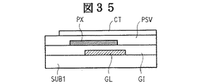
図34に示すように、画素電極PXの延在部は絶縁膜GIを介してゲート信号線GLの一部に重畳されて容量素子Caddを形成するとともに、保護膜PSVを介して前記基準電極CTの延在部にも重畳されて容量素子Cstgを形成している。なお、図35は図34の35−35線における断面を示した図である。
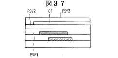
(実施例38)
また、図35に示す実施例に対する他の実施例を図36に示すように、保護膜PSVが無機材料と有機材料との順次積層体(PSV1、PSV2)で構成されている場合、容量素子Cstgの容量を充分確保できないことから、容量素子Caddを併用させた構成とすることは有益となる。
【0199】
また、図36に対応する図37に示すように、基準電極CTの上面にさらに保護膜PSV3が形成されていてもよいことはもちろんである。
(実施例39)
また、上述した構成から、容量素子Cstgと容量素子Caddはほぼ同じ領域内に形成され、換言すれば各素子Cstg、Caddは重畳されて形成されているため、それらの占有面積を小さくでき開口率の向上を図ることができる。
(実施例40)
また、上述した構成から、容量素子Cstgの面積より容量素子Caddの面積を小さく形成することにより、必要な容量を確保しつつ、より電気的に安定な容量素子Cstgでの保持の役割を確保して保持電位の安定化を図ることができる。
(実施例41)
また、上述した構成から、画素電極PXの延在部は他の隣接する画素電極PXとの接続部とゲート信号線GLの一部と重畳する部分(容量素子Cadd形成部)とで構成しているため、たとえば該容量素子Caddの形成部にてショートが生じた場合、ゲート信号線と重畳する部分を他の部分とたとえばレーザ光線によって切り離すことによって、救済を図ることができる。
【0200】
この場合、容量素子Cstgによって一定の容量が確保でき、該画素の画質の低下を抑制できる。
(実施例42)
また、実施例41の場合において、基準電極CTを一部とする材料層を光透光性の材料層で構成することにより、該容量素子Caddの形成部にて生じるショートを容易に目視できる効果を奏する。
(実施例43)
上述した実施例37〜42に示した効果は、図38に示すように、基準信号線を形成し、この基準信号線と基準電極をスルホールによって接続させた構成の場合においても同様に適用できる。
(実施例44)
図39は、上述した実施例37ないし43の構成をいわゆるマルチドメイン方式に適用した場合の構成を示している。
【0201】
マルチドメイン方式とは、画素電極PXと基準電極CTとの間に発生する電界の方向を画素領域内に2個形成するようにし、これにより、表示面の垂直方向に対して異なる方向から観察しても色調の変化が生じないようにしたものである。
【0202】
そのための一実施例として、画素電極および基準電極をそれぞれその延在方向に沿って複数の屈曲部を形成してジグザグ形状としたものである。
【0203】
なお、本実施例では、図39として、容量素子Caddを構成した例を示したが、容量素子Cstgのみの場合であっても適用できる。
(実施例45)
図40は実施例44の構成にゲート信号線GLと平行に基準電圧信号線CLを設け、絶縁膜に形成されたスルホールTHを通して基準電極CTに接続された構成となっている。
(実施例46)
図41は実施例44の構成において、ドレイン信号線DLをその上層に形成されている基準電極CTの形状に対応させてその走行方向にジグザグ状にしたものである。
【0204】
これにより基準電極CTは、ドレイン信号線DLを均一な幅で被うことになり、該ドレイン信号線DLからの電界の基準電極CT側への終端を信頼性よく行うことができるようになる。
(実施例47)
この実施例は、図42に示すように、上述の実施例46の構成において基準電圧信号線CLを備えた構成とするとともに、スルホールTHを通して接続される基準電極CTの該接続部の幅を広く形成している。
(実施例48)
この実施例は、実施例23ないし26の各構成において、薄膜トランジスタTFTのバックチャネルの発生を回避するため、基準電極CTを一部として構成する導電膜の該薄膜トランジスタTFT上の領域において開口を設けた構成としたものである。
(実施例49)
この実施例は、実施例37ないし48の各構成において、基準電極CTとして、Al、Cr、Mo、Ta、Wのいずれかの材料、あるいはそれらの合金からなる材料、あるいはそれらのいくつかを積層させた材料を用いたものである。
【0205】
このようにすることによって、ドレイン信号線DL上の遮光膜の特別の形成を不要とし、また、低抵抗となるためコモン反転駆動での波形歪みを抑制できるようになる。
(実施例50)
この実施例は、実施例37ないし48の各構成において、基準電極CTとして、Al、Cr、Mo、Ta、Wのいずれかの材料、あるいはそれらの合金からなる材料、あるいはそれらのいくつかを積層させた材料を用いるととともに、基準電圧信号線CLとして、Al、Crのいずれかの材料、あるいはそれらの合金からなる材料、あるいはそれらのいくつかを積層させた材料を用いたものである。
(実施例51)
この実施例は、基準電極CTとして、ITO、In2O3、SnO2、IZO、ZnO2いずれかの材料、あるいはそれらの合金からなる材料、あるいはそれらのいくつかを積層させた材料を用いたものである。
【0206】
この場合、ゲート信号線GL、ドレイン信号線DL、基準電圧信号線CLの端子部において、電食を防止するために上記材料を被覆する構成とした場合、該基準電極の形成はそれと同時に行うことができ、製造工数の増大を回避することができる。
【0207】
また、この場合、容量素子の修復の際において、該容量素子を該基準電極CTを通して直接に目視できるので、レーザ切断によるリペア時の位置決めが容易となる効果を奏する。
(実施例52)
この実施例は、実施例51の構成において、いわゆるノーマリブラックモードとなっていることにある。
【0208】
これにより、ドレイン信号線上の基準電極CTは遮光膜として機能し、たとえばノーマリホワイトモードで構成した場合と比較して、光漏れによる不都合を解消することができる。
【0209】
ここで、ノーマリホワイトモードとは、画素電極PXと基準電極CTとの間に電界を発生せしめた場合、液晶の光透過率が最高となる構成をいう。
(実施例53)
この実施例は、実施例51、52の各構成において、いわゆるドット反転駆動で基準電極CTと画素電極PXとの間に電圧を印加することにある。
【0210】
基準電極CTが上述した材料(ITO、In2O3、SnO2、IZO、ZnO2等)で構成しその抵抗が比較的高くなることに鑑み、該ドット反転を行うことにより、表示面の輝度の均一化を向上させるようにするものである。
(実施例54)
この実施例は、上述した各構成のうち、薄膜トランジスタTFTの上方に基準電極CTを一部とする導電層が形成されたもの(開口が形成されていないもの)において、基準電極をその電位が(−)5V以上(+)10V以下の範囲内となるように駆動させることにある。
【0211】
このようにした理由は、上記範囲での基準電極の駆動は、薄膜トランジスタTFTのしきい値の変動が許容範囲内に抑えられることが判明したからである。
(実施例55)
上述した各実施例では、画素内に形成されるスイッチング素子として薄膜トランジスタTFTに限定されることなく他の構成のスイッチング素子にも適用できる。
【0212】
しかし、薄膜トランジスタTFTを適用した場合、それをON状態とするのにゲート信号線に供給する走査信号は+12V以上、OFF状態とするためには−5V以下に設定されている。
【0213】
このため、基準電極CTの電位を該条件にかからない領域として駆動することにより、この基準電極CTによって該薄膜トランジスタTFTの誤動作を防止できる。
(実施例56)
この実施例では、上述した各構成のうち、薄膜トランジスタTFTの上方に基準電極を一部とする導電層が形成されたもの(開口が形成されていないもの)において、いわゆるコモン反転駆動方法において、該基準電極の電位の最小値を−5V以上としたものである。
【0214】
このようにした場合においても、薄膜トランジスタTFTのしきい値変動を抑制させることができる。
(実施例57)
この実施例では、上述した各構成のうち、薄膜トランジスタTFTの上方に基準電極CTを一部とする導電層が形成されたもの(開口が形成されていないもの)において、基準電極の電位をほぼ一定とする駆動において、その電位を−5V以上+10V以下の範囲、望ましくは−1V以上+7V以下の範囲に設定したものである。
【0215】
このようにした場合においても、薄膜トランジスタTFTのしきい値変動を抑制させることができる。
(実施例58)
この実施例は、たとえばゲート信号線GLのゲート駆動IC5の接続近傍の構成を示したものである。
【0216】
図43に示すように、ゲート信号線GLのゲート駆動IC5の接続近傍は、上述したように、隣接する他のゲート信号線GLととともにゲート駆動IC5側に収束するパターンとして形成されている。なお、この部分は図58の一点鎖線枠Aに囲まれる部分に対応している。
【0217】
この場合において、各ゲート信号線GLの間に基準電圧信号線CLが同層で配置され、この基準電極信号線CLもゲート駆動IC5側に引き出す場合、各ゲート信号線GLの前記収束する領域にて隣接するゲート信号線GLと干渉し、ショートを起こし易くなる。
【0218】
このため、この実施例では、基準電圧信号線CLはゲート信号線GLに対して絶縁膜を介した他の層で形成するとともに、各ゲート信号線GLの前記収束する領域にて該ゲート信号線GLとほぼ直交する方向に延在する配線層50と前記絶縁膜に形成したスルホールを通して接続させる構成としたものである。
【0219】
このように構成することによって、いわゆる額縁と称される領域の増大を回避することができる。
【0220】
すなわち、先の例で、基準電圧信号線CLを各ゲート信号線GLの前記収束する領域にてショートなく形成しようとした場合、該収束の部分の各ゲート信号線の屈曲角度を小さく形成しなければならず、それだけゲート駆動IC5を表示領域ARから遠のく位置に実装しなければならないからである。
【0221】
なお、この実施例の画素としてたとえば図13に示すように構成した場合に、前記配線層50はドレイン信号線DLと同時に形成する配線層とすることができる。
【0222】
また、この実施例では、ゲート信号線GLのゲート駆動IC5の接続近傍の構成を示したものであるが、ドレイン信号線DLのドレイン駆動IC6の接続近傍においても適用できることはもちろんである。
(実施例59)
この実施例は、図43(b)に対応する図44に示すように、前記配線層50を基準電圧信号線CLと一体に形成したものである。
(実施例60)
この実施例は、実施例58に示す構成において、画素領域における構成をも示した図である。すなわち、ゲート信号線GLと基準電圧信号線CLとを同層に形成し、絶縁膜を介して該絶縁膜の上面に形成された基準電極CTと該絶縁膜に形成されたスルホールTHによって接続されている。
(実施例61)
この実施例は、実施例59に示す構成において、やはり画素領域における構成をも示した図である。
(実施例62)
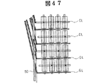
図47は、図43に対応する図であり、図43と異なる構成は、配線層50に引き出される基準電圧信号線CLは、一つ置きに配置されたものとなっている。この場合、一つ置きに限定されることはなく、二つ置き、あるいは三つ置き等であってもよいことはいうまでもない。
【0223】
なお、この場合において、基準電極CTは、上述したように材料層の一部として形成されるもので、この材料層は隣接する他の画素領域における対応する材料層と接続されて形成されるようになっている。
【0224】
このように構成した場合、各ゲート信号線GLが収束する領域において、信号線の密集を回避できるようになる。
【0225】
なお、この実施例では基準電圧信号線について説明したものであるが、たとえば保持容量線においても適用できることはいうまでもない。
(実施例63)
この実施例では、図48に示すように、前記配線層50は一つのドライバチップ(ドレイン駆動IC6、ゲート駆動IC5)に接続される各ゲート信号線GLの束の外側を迂回し、さらに、該ドライバチップに隣接して引き出されるように構成されている。
【0226】
このように構成した場合、該配線層50を該ドライバチップの入力側の端子側に引き出せるようにできる。
【0227】
なお、図48に示す部分は図58に示す一点鎖線枠Bに示す部分に対応している。
(実施例64)
この実施例では、図48に対する他の実施例を示すもので、図49に示すように、ドライバチップに隣接して引き出される配線層50はドライバチップの下側に位置するように構成されている。
(実施例65)
この実施例では、上述した各実施例の構成において、配向膜ORI1、ORI2として、下記の構造式からなる材料を用いていることにある。
【0228】
【化5】

【化6】
このような配向膜ORI1、ORI2を用いることにより、液晶層内のイオン性不純物の移動による残像(イオン性残像)の発生を抑制できるようになる。
【0231】
さらに、配向膜中の式(1)および式(2)の物質の合計の成分比に対し、式(1)の物質が30%〜70%の割合である場合に、さらに発生を抑制できるようになる。
【0232】
ここで、イオン性残像とは、図50(a)に示すように、初期状態で隣接する領域に白および黒の表示を1時間行い、その表示を中間調で表示、その輝度変化を白表示の領域から黒表示の領域にわたって検出した際の該中間調に対応する輝度から突出した輝度の部分をいう。
【0233】
この場合、前記配向膜ORI1、ORI2として上述した材料を用いることによって、図50(a)に示すイオン性残像強度を3以下(好ましくは2以下)に抑えることができ、イオン性残像の回避を達成することができる。
【0234】
なお、図50(b)は、図50(a)の初期の黒の表示を共通の部分とし、その右側に白の表示があることを示している。
【0235】
図50(a)の場合と比べて中間調における輝度分布が異なるのはイオンが図中左側へ移動する現象が見られるからである。
(実施例66)
この実施例では、たとえば図31の構成において、その(b)に対応する図51(a)に示すように、基準電極CTが保護膜PSV(その上層が有機材料からなる保護膜PSV2)上に形成され、該基準電極CTをも被って該保護膜PSV上に配向膜ORI1が形成されている。
【0236】
そして、該保護膜PSVの上面の該基準電極CTが形成されている部分に凹陥部が形成されている。
【0237】
これにより、該基準電極CTの段差を極力小さくし、前記配向膜ORI1の該基準電極CTの近傍におけるラビング性の低下、および残像悪化、配向不良による光ぬけを解消した構成となっている。
【0238】
この場合、図51(b)に示すように、電極の厚さをH(=300nm)、凹陥部にから突出した電極の高さをH1(=0、90、150、300nm)とした場合、それぞれの電極の光抜けの状態を調査した結果、図52に示すようになった。図中、◎は光抜けの回避が最も良い状態、○は良好な状態、×は良好でない状態を示している。
【0239】
このことから、該基準電極CTは保護膜PSV2に埋め込ませた構成とすることがよく、該基準電極CTの厚さをH1、凹陥部から突出した電極の高さをH2は次式(3)に示す関係にあることが好ましいことがわかる。
【0240】
【数11】
0≦(H−H1)/H≦0.5 ……(3)
そして、この実施例では、基準電極CTの表面に直接配向膜ORI1を形成した場合について説明したものである。しかし他の絶縁膜を形成しその表面に配向膜ORI1を形成した構成の場合にも適用できる。
【0241】
この場合、基準電極CTによる段差が前記他の絶縁膜の表面に顕在化した段差におけるその高さをH1として換算すればよい。
【0242】
なお、この場合の電極として基準電極CTに限定されることはなく、他の電極であってもよく、また、透光性あるいは非透光性の材料層に限定されることはない。
(実施例67)
この実施例では、上述した各実施例で、保護膜PSVを無機材料からなる保護膜PSV1と有機材料からなる保護膜PSV2の順次積層体で形成する場合において、該保護膜PSV2の材料として、アクリル系(透明性が高い、ポジ型感光性)、ポリイミド系(耐熱性が高い)、ノボラック系(着色し易い)、ポリイミド−エポキシ共重合体(配向膜を兼用しうる)のいずれか、あるいはそれらの積層体を用いていることにある。
【0243】
このような保護膜PSV2は、膜厚400nmで95%の透光性、230℃以上の耐熱性を有する。
【0244】
また、液晶に対する汚染性が低く、耐プロセス性(スパッタ、エッチング液、剥離液、配向膜溶媒、UV/O3洗浄に耐える)を有する。
(実施例68)
画素電極PXと基準電極CTとの間に電圧を印加して電界を形成する場合、それら各電極との間に有機材料の保護膜PSV2が介在されている場合、該保護膜PSV2による駆動電圧を増加せざるを得ないことが確かめられる。
【0245】
この場合、ドライバ、すなわちゲート信号線GLに走査信号を供給するゲート駆動IC5、あるいはドレイン信号線DLに映像信号を供給するドレイン駆動IC6が、透明基板SUB1に直接実装されている場合(FCA方式)において、該駆動ICの発熱対策が必要となる。
【0246】
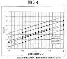
そこで、ノーマリブラックモードで最大輝度となる液晶駆動電圧Vmaxを有機材料からなる保護膜PSV2の膜厚、画素電極Pxと基準電極CTとの間隔、液晶の誘電率異方性との関係を究明した。
【0247】
まず、液晶の誘電率異方性、画素電極PXと基準電極CTとの間隔、Vmaxとの関係を示すグラフである図53、液晶の誘電率異方性=10での保護膜PSV2の膜厚、画素電極PXと基準電極CTとの間隔、Vmaxとの関係を示すグラフである図54、液晶の誘電率異方性=14.5での保護膜PSV2の膜厚、画素電極PXと基準電極CTとの間隔、Vmaxとの関係を示すグラフである図55を得た。
【0248】
このことから、図53に示すように、液晶の誘電率異方性の高い液晶材料を用いることによりVmaxを低減できる。そして、保護膜PSV2の膜厚の増加ととともにVmaxは増大し、画素電極PXと基準電極CTとの間隔の増加ととともにVmaxは増大する。この関係は図54、および図55に示される。
【0249】
従って、上述のグラフから次式(4)の関係が成立することが導かれる。
【0250】
【数12】
Vmax=1.9d+0.4146W−0.2328Δε+2.8218 ……(4)
ここで、dは有機材料からなる保護膜PSV2の膜厚(μm)、Wは画素電極Pxと基準電極CTとの間隔(μm)、Δεは液晶の誘電率異方性を示している。
【0251】
このことから、まず、高いΔεを有する液晶の材料としては、図55の化学構造式に示すようにシアノジフッ素液晶を用いるのが望ましく、また、Δεが14.5以上のような高い領域を実現するには、図57の化学構造式に示すようにトリフッ素ジオキサン液晶を用いるのが望ましい。
【0252】
いずれにしても、上記各液晶のうち少なくとも一方を含む液晶を用いることにより、上記Vmaxを低減できることになる。
(実施例69)
ノーマリブラックモードの構成において、画素電極PXと基準電極CTとが有機材料からなる保護膜PSV2を介して異なる層にある場合、白表示の際のドレインドライバの出力電圧の振幅を片側7.5V以下とすることによって、液晶表示を可能ならしめる。
(実施例70)
また、ノーマリブラックモードの構成において、画素電極PXと基準電極CTとが有機材料からなる保護膜PSV2を介して異なる層にある場合、上記式(4)が15Vより小さくなるようにd、W、Δεを設定し、さらに、いわゆるコモン反転を行い、白表示の際のドレインドライバの出力電圧の振幅を片側7.5V以下とすることによって、液晶表示を可能ならしめる。
【0253】
これは、コモン反転駆動によれば、同じ液晶駆動電圧を得るのに必要なドライバの出力電圧をほぼ半減できるからである。
(実施例71)
また、ノーマリブラックモードの構成において、画素電極PXと基準電極CTとが有機材料からなる保護膜PSV2を介して異なる層にある場合、上記式(4)が7.5Vより小さくなるようにd、W、Δεを設定し、さらに、白表示の際のドレインドライバの出力電圧の振幅を片側7.5V以下とすることによって、液晶表示を可能ならしめる。
(実施例72)
また、ノーマリブラックモードの構成において、画素電極PXと基準電極CTとが有機材料からなる保護膜PSV2を介して異なる層にある場合、映像信号の電圧最大振幅を前記液晶層の相対透過率を90%とするのに要する電圧以下に設定することによって、上記式(4)が9.375Vより小さい場合において、白表示の際のドレインドライバの出力電圧の振幅を7.5V以下として、液晶表示を可能ならしめる。
【0254】
これは、ノーマリブラックモードにおいては、Vmax近辺でB−Vのカーブが緩やかになるため、透過率100を得るのに要する電圧に対し、透過率90%を得るのに要する電圧はその80%で済むことによる。
(実施例73)
また、ノーマリブラックモードの構成において、画素電極PXと基準電極CTとが有機材料からなる保護膜PSV2を介して異なる層にある場合、いわゆるコモン反転を行い、映像信号の電圧最大振幅を前記液晶層の相対透過率を90%とするのに要する電圧以下に設定することによって、上記式(4)が18.75Vより小さい場合において、白表示の際のドレインドライバの出力電圧の振幅を7.5V以下として、液晶表示を可能ならしめる。
(実施例74)
ノーマリブラックモードの構成において、画素電極PXと基準電極CTとが有機材料からなる保護膜PSV2を介して異なる層にある場合、白表示の際のドライバの出力電圧の振幅を片側5V以下とすることによって、ドレインドライバの発熱の対策を図る。
(実施例75)
また、ノーマリブラックモードの構成において、画素電極PXと基準電極CTとが有機材料からなる保護膜PSV2を介して異なる層にある場合、いわゆるコモン反転を行い、白表示の際のドレインドライバの出力電圧の振幅を片側5V以下とし、かつ上記式(4)を10Vより小さくなるようにd、W、Δεを設定し、ドライバの発熱の対策を図る。
(実施例76)
また、ノーマリブラックモードの構成において、画素電極PXと基準電極CTとが有機材料からなる保護膜PSV2を介して異なる層にある場合、いわゆるコモン反転を行い、白表示の際のドレインドライバの出力電圧の振幅を片側5V以下とし、かつ上記式(4)を10Vより小さくなるようにd、W、Δεを設定することによって、ドライバの発熱の対策を図る。
(実施例77)
また、ノーマリブラックモードの構成において、画素電極PXと基準電極CTとが有機材料からなる保護膜PSV2を介して異なる層にある場合、映像信号の電圧最大振幅を前記液晶層の相対透過率を90%とするのに要する電圧以下に設定することによって、上記式(4)が6.25Vより小さい場合において、白表示の際のドレインドライバの出力電圧の振幅を片側5V以下とし、ドライバの発熱の対策を図る。
(実施例78)
また、ノーマリブラックモードの構成において、画素電極PXと基準電極CTとが有機材料からなる保護膜PSV2を介して異なる層にある場合、いわゆるコモン反転を行い、映像信号の電圧最大振幅を前記液晶層の相対透過率を90%とするのに要する電圧以下に設定して、上記式(4)が12.5Vより小さい場合において、白表示の際のドレインドライバの出力電圧の振幅を片側5V以下として、ドライバの発熱の対策を図る。
【0255】
【発明の効果】
以上説明したことから明らかなように、本発明による液晶表示装置によれば、ドライバ近傍の液晶の局所的温度上昇を抑制させた液晶表示装置を得ることができる。
【0256】
また、ドライバの基板に対する応力の伝達を抑制させた液晶表示装置を得ることができる。
【0257】
また、ドライバ近傍の表示面にてアライメントずれを抑制させた液晶表示装置を得ることができる。
【0258】
また、開口率を向上せた液晶表示装置を得ることができる。
【0259】
さらに、いわゆる額縁の縮小を図った液晶表示装置を得ることができる。
【図面の簡単な説明】
【図1】本発明による液晶表示装置の一実施例を示す説明図で、ノーマリブラックモードにおける液晶駆動電圧と相対輝度との関係を示したグラフである。
【図2】本発明による液晶表示装置の一実施例を示す全体構成図である。
【図3】本発明による液晶表示装置の画素の一実施例を示す平面図である。
【図4】図3のIV−IV線における断面図である。
【図5】図3のV−V線における断面図である。
【図6】ノーマリホワイトモードにおける液晶駆動電圧と相対輝度との関係を示したグラフである。
【図7】コモン反転における画素電極と基準電極との間の電圧値を時間との関係で示したグラフである。
【図8】コモン電圧一定における画素電極と基準電極との間の電圧値を時間との関係で示したグラフである。
【図9】信号線に伝達する際の信号の歪みの発生を示した説明図である。
【図10】信号線に接続されるドライバ(ゲート駆動IC、ドレイン駆動IC)およびその近傍の構成を示す側面図である。
【図11】液晶表示装置の表示領域のうちドライバに近接する部分に変色が生じることを示す説明図である。
【図12】液晶表示装置の液晶を介して対向配置させる各基板の間に配置される支柱の一実施例を示す構成図である。
【図13】本発明による液晶表示装置の画素の他の実施例を示す構成図である。
【図14】本発明による液晶表示装置に形成される基準電極の一実施例を示す平面図である。
【図15】本発明による液晶表示装置の画素の他の実施例を示す構成図である。
【図16】本発明による液晶表示装置の画素の他の実施例を示す構成図である。
【図17】本発明による液晶表示装置の画素の他の実施例を示す構成図である。
【図18】本発明による液晶表示装置の画素の他の実施例を示す構成図である。
【図19】本発明による液晶表示装置の画素の他の実施例を示す構成図である。
【図20】本発明による液晶表示装置の画素の他の実施例を示す構成図である。
【図21】本発明による液晶表示装置の画素の他の実施例を示す構成図である。
【図22】本発明による液晶表示装置の画素の他の実施例を示す構成図である。
【図23】本発明による液晶表示装置の画素内に形成されるスルホールの一実施例を示す断面図である。
【図24】本発明による液晶表示装置の画素内に形成されるスルホールの他の実施例を示す断面図である。
【図25】本発明による液晶表示装置の画素内に形成されるスルホールの他の実施例を示す断面図である。
【図26】本発明による液晶表示装置の画素内に形成されるスルホールの他の実施例を示す断面図である。
【図27】本発明による液晶表示装置の画素内に形成されるスルホールの配置の実施例を示す断面図である。
【図28】本発明による液晶表示装置の画素内に形成されるスルホールの他の実施例を示す断面図である。
【図29】本発明による液晶表示装置の画素の他の実施例を示す構成図である。
【図30】本発明による液晶表示装置の画素の他の実施例を示す構成図である。
【図31】本発明による液晶表示装置の画素の他の実施例を示す構成図である。
【図32】本発明による液晶表示装置の画素の他の実施例を示す構成図である。
【図33】本発明による液晶表示装置の画素の他の実施例を示す構成図である。
【図34】本発明による液晶表示装置の画素の他の実施例を示す構成図である。
【図35】図34の35−35線における断面図である。
【図36】本発明による液晶表示装置の他の実施例を示す図で、図35に対応する図である。
【図37】本発明による液晶表示装置の他の実施例を示す図で、図35に対応する図である。
【図38】本発明による液晶表示装置の画素の他の実施例を示す構成図である。
【図39】本発明による液晶表示装置の画素の他の実施例を示す構成図である。
【図40】本発明による液晶表示装置の画素の他の実施例を示す構成図である。
【図41】本発明による液晶表示装置の画素の他の実施例を示す構成図である。
【図42】本発明による液晶表示装置の画素の他の実施例を示す構成図である。
【図43】本発明による液晶表示装置の他の実施例を示す構成図で、各基準電圧信号線の引出部を示した平面図である。
【図44】本発明による液晶表示装置の他の実施例を示す構成図で、各基準電圧信号線の引出部を示した断面図である。
【図45】本発明による液晶表示装置の他の実施例を示す構成図で、各基準電圧信号線の引出部を示した断面図である。
【図46】本発明による液晶表示装置の他の実施例を示す構成図で、各基準電圧信号線の引出部を示した断面図である。
【図47】本発明による液晶表示装置の他の実施例を示す構成図で、各基準電圧信号線の引出部を示した断面図である。
【図48】本発明による液晶表示装置の他の実施例を示す構成図で、ドライバの実装部分の近傍を示す平面図である。
【図49】本発明による液晶表示装置の他の実施例を示す構成図で、ドライバの実装部分の近傍を示す平面図である。
【図50】液晶内のイオン性残像の現象およびイオン性残像強度を示す説明図である。
【図51】本発明による液晶表示装置の他の実施例を示す構成図である。
【図52】図51に示した構成において電極の絶縁膜に対する埋込具合と該電極近傍の光抜け具合の関係を示したグラフである。
【図53】液晶の誘電率異方性、画素電極と基準電極との間隔、電極間電圧Vmaxとの関係を示すグラフである。
【図54】液晶の誘電率異方性=10での有機材料からなる保護膜の膜厚、画素電極と基準電極との間隔、Vmaxとの関係を示すグラフである。
【図55】液晶の誘電率異方性=14.5での有機材料からなる保護膜の膜厚、画素電極と基準電極との間隔、Vmaxとの関係を示すグラフである。
【図56】本発明による液晶表示装置に用いられる液晶中に含まれる液晶の一実施例を示す化学構造式である。
【図57】本発明による液晶表示装置に用いられる液晶中に含まれる液晶の一実施例を示す化学構造式である。
【図58】本発明による液晶表示装置のドライバの実装領域の近傍を示した平面図である。
【符号の説明】
AR……表示領域、SUB……透明基板、GL……ゲート信号線、DL……ドレイン信号線、CL……基準電圧信号線、PX……画素電極、CT……基準電極、TFT……スイッチング素子(薄膜トランジスタ)、TH……スルホール、GI……絶縁膜、PSV……保護膜、PSV1……無機材料からなる保護膜、PSV2……有機材料からなる保護膜、33……支柱、5……ゲート駆動IC(ドライバ)、6……ドレイン駆動IC(ドライバ)、ORI……配向膜、BM……ブラックマトリクス、OC……平坦化膜。[0001]
BACKGROUND OF THE INVENTION
The present invention relates to a liquid crystal display device, and more particularly to an active matrix liquid crystal display device.
[0002]
[Prior art]
The active matrix type liquid crystal display device includes a gate signal line and y extending in the x direction and arranged in parallel in the y direction on the liquid crystal side surface of one of the substrates opposed to each other through the liquid crystal. Each region surrounded by drain signal lines extending in the direction and arranged in parallel in the x direction is defined as a pixel region, and in this pixel region, an active element operated by a scanning signal from the gate signal line, and an active element interposed therebetween A pixel electrode to which a video signal is supplied from the drain signal line, and a capacitor formed between the pixel electrode.
[0003]
Such a liquid crystal display device realizes pixel display by performing writing for a certain time and holding for a certain time by an active element.
[0004]
As this retention method, a Cadd (additional capacitance) method in which a capacitance is formed between the gate signal line and the pixel electrode and a Cstg (retention capacitance) method in which a capacitance is formed between the retention capacitance signal line and the pixel electrode are known. ing.
[0005]
The Cstg method requires a storage capacitor signal line and thus decreases the aperture ratio. However, since the storage potential can be stabilized, a relatively high image quality can be obtained.
[0006]
A liquid crystal display device using the Cstg method is known as a so-called lateral electric field method. This type of liquid crystal display device is configured by providing a reference electrode for generating an electric field between the pixel electrode and a reference signal line for supplying a reference signal to the reference electrode. A storage capacitor is formed by overlapping pixel electrodes with an insulating film interposed therebetween.
[0007]
In recent years, products using this method have been commercialized as devices capable of realizing a wide viewing angle of liquid crystal display devices.
[0008]
On the other hand, in order to ensure a uniform gap (cell gap) between the substrates arranged opposite to each other through the liquid crystal, a structure in which polymer static beads are dispersed in the liquid crystal, or selective etching by photolithography technology on one substrate surface. A configuration in which organic material columns are provided is known.
[0009]
Although light leaks around the beads or pillars, the position of the pillars in the screen can be set in advance, so that the contrast ratio can be improved compared to the technique using beads dispersion.
[0010]
As a mounting of a driver (semiconductor chip) for supplying a signal to an active element, a TCP method and an FCA (also referred to as COG) method are known.
[0011]
The TCP method has features that it can be manufactured more easily than the FCP method and the yield can be improved. In addition, since the FCP method can reduce the number of lead-out wirings to the outside, it is suitable for high definition.
[0012]
[Problems to be solved by the invention]
(Problem 1)
First, in order to realize a wide viewing angle and high-definition liquid crystal display device, it is desirable to adopt the FCA method for the above-mentioned lateral electric field method.
[0013]
However, in the lateral electric field method, since the liquid crystal display mode is a birefringence mode, it is more sensitive to variations in the thickness of the liquid crystal layer than, for example, the TN mode, and more colored with respect to the same amount of variation in the liquid crystal layer thickness. It has the disadvantage of being visible.
[0014]
In the FCA method, since the driver is directly mounted on the substrate of the liquid crystal display device, the heat generated from the driver is directly transmitted to the substrate of the liquid crystal display device, causing a local temperature rise in the liquid crystal near the driver. Invited and found that this part appears to be discolored.
(Problem 2)
In addition, when the FCA method is adopted, a driver composed only of a semiconductor chip is often mounted on a substrate of a liquid crystal display device as it is, and stress is likely to be generated on a substrate around the semiconductor chip.
[0015]
Then, it was found that this stress causes inconvenience that the portion near the driver on the display surface looks discolored.
[0016]
In this case, in the so-called normally black mode, it was confirmed that light leakage occurred during black display, leading to a decrease in contrast ratio. Here, the normally black mode refers to a mode in which the light transmittance of the liquid crystal is minimized when no electric field is applied to the liquid crystal.
(Problem 3)
In addition, in order to make the gaps between the substrates facing each other through the liquid crystal uniform, when the support is formed on the substrate on one side, the upper and lower substrates are combined in the region near the chip due to the stress shown in the
[0017]
When beads are used, the shape of the beads is spherical and not firmly fixed, so that when local stress is applied, the beads are rearranged in a direction that relaxes them, resulting in the semiconductor chip. Misalignment between the upper and lower substrates in the vicinity is reduced.
[0018]
However, in the case of a pillar, since the pillar and the substrate are in surface contact and the contact area is large, and the pillar itself is fixed to the substrate on one side, the local misalignment in the vicinity of the semiconductor chip due to stress remains as it is and mitigates. It will not be done.
(Problem 4)
Further, in the case of the horizontal electric field method, it is known that the reference electrode is disposed adjacent to the video signal line among the pixel electrode and the reference electrode that generate an electric field.
[0019]
This is because the electric field from the video signal line is terminated on the reference electrode side so as not to affect the pixel electrode side.
[0020]
A gap is formed between the video signal line and the reference electrode, and the liquid crystal is driven in the gap to generate a so-called domain. Therefore, a light shielding film is formed in this portion.
[0021]
However, it has been pointed out that the formation of the light shielding film hinders improvement of the aperture ratio of the pixel.
(Problem 5)
Further, in connection with the driver of the gate signal line or the drain signal line, the signal line in the vicinity of the driver is formed as a pattern narrowed down to the size of the semiconductor chip.
[0022]
In this case, a signal line other than the above, for example, a reference signal line is also required to be drawn out to the semiconductor chip side and connected to another wiring layer at the narrowed portion of each signal line. Securement is required.
[0023]
However, there is an inconvenience that the reduction of the so-called frame (the portion formed by the width from the outer contour of the substrate to the display surface) cannot be ensured because of the area for that purpose.
[0024]
An object of the present invention is to provide a liquid crystal display device in which the inconvenience shown in the
[0025]
An object of the present invention is to provide a liquid crystal display device in which the inconvenience shown in the
[0026]
An object of the present invention is to provide a liquid crystal display device in which the misalignment is suppressed on the display surface in the vicinity of the driver in order to eliminate the inconvenience shown in the
[0027]
An object of the present invention is to provide a liquid crystal display device in which the inconvenience shown in the above problem 4 is solved, that is, the aperture ratio is improved.
[0028]
An object of the present invention is to provide a liquid crystal display device in order to eliminate the inconvenience shown in the
[0029]
[Means for Solving the Problems]
Of the inventions disclosed in the present invention, the outline of typical ones will be briefly described as follows.
[0030]
As a typical means for solving the above-mentioned
In each of the pixel regions, a switching element operated by a scanning signal from a gate signal line, a pixel electrode to which a video signal from a drain signal line is supplied via the switching element, and an electric field between the pixel electrode And a reference electrode that generates
The video signal from the drain signal line is made by a driver chip mounted on the one substrate,
When the voltage between the pixel electrode and the reference electrode is not applied, the light transmittance of the liquid crystal layer is configured to be the lowest,
The maximum voltage amplitude of the video signal is set to be equal to or lower than a voltage required for setting the relative transmittance of the liquid crystal layer to 90%.
[0031]
As a typical means for solving the above-mentioned
In each of the pixel regions, a switching element operated by a scanning signal from a gate signal line, a pixel electrode to which a video signal from a drain signal line is supplied via the switching element, and an electric field between the pixel electrode And a reference electrode that generates
The video signal from the drain signal line is made by a driver chip mounted on the one substrate,
A stress buffer layer is interposed between the driver chip and the one substrate.
[0032]
As a typical means for solving the above-mentioned
In each of the pixel regions, a switching element operated by a scanning signal from a gate signal line, a pixel electrode to which a video signal from a drain signal line is supplied via the switching element, and an electric field between the pixel electrode And a reference electrode that generates
The signal from each signal line is made by a driver chip mounted on the one substrate,
A support for securing a gap with the other substrate facing the liquid crystal side surface of any one of the substrates,
The support columns are arranged at a density of 1 or less per two adjacent pixel regions.
[0033]
As a typical means for solving the above problem 4, for example, on the liquid crystal side surface of one of the substrates that are arranged to face each other with a liquid crystal layer interposed therebetween,
In each of the pixel regions, a switching element operated by a scanning signal from a gate signal line, a pixel electrode to which a video signal from a drain signal line is supplied via the switching element, and an electric field between the pixel electrode A plurality of reference electrodes that cause
One of the reference electrodes is formed so as to overlap with the drain signal line through an insulating film having a dielectric constant lower than that of the inorganic material, and the width of the reference electrode is larger than the width of the drain signal line. It is characterized by being.
[0034]
As a typical means for solving the above-mentioned
In each of the pixel regions, a switching element operated by a scanning signal from the gate signal line, a pixel electrode to which a video signal from the drain signal line is supplied via the switching element, and a space apart from the pixel electrode And a reference electrode to which a reference signal from a reference signal line is supplied,
The video signal from the drain signal line is made by a driver chip mounted on the one substrate,
The gate signal line, the drain signal line, and the reference signal line are each formed in different layers with an insulating film interposed therebetween.
[0035]
DETAILED DESCRIPTION OF THE INVENTION
Hereinafter, embodiments of a liquid crystal display device according to the present invention will be described with reference to the drawings.
Example 1
[Equivalent circuit of liquid crystal display]
FIG. 2 is an equivalent circuit diagram showing an embodiment of the liquid crystal display device according to the present invention. Although this figure is a circuit diagram, it is drawn corresponding to the actual geometric arrangement.
[0036]
In this embodiment, the present invention is applied to a liquid crystal display device adopting a so-called lateral electric field method that is known to have a wide viewing angle.
[0037]
First, there is a liquid crystal display panel PNL, and the liquid crystal display panel PNL uses the transparent substrates SUB1 and SUB2 arranged opposite to each other via liquid crystal as an envelope. In this case, one transparent substrate (lower substrate in the figure: matrix substrate) is formed slightly larger than the other transparent substrate (upper substrate in the figure: color filter substrate), and the lower and right peripherals in the figure The ends are arranged almost flush with each other.
[0038]
As a result, the periphery on the left side in the drawing and the periphery on the upper side in the drawing of one transparent substrate SUB1 extend outward with respect to the other base transparent plate SUB2. As will be described in detail later, this portion is a region where a gate drive circuit (IC) 5 and a drain drive circuit (IC) 6 are mounted.
[0039]
In the region where the transparent substrates SUB1 and SUB2 overlap each other,
[0040]
Here, as described above, each
[0041]
Each gate signal line GL has one end (the left end in the figure) extending outside the transparent substrate SUB1, and is connected to the output terminal of the
[0042]
In this case, a plurality of
[0043]
Similarly, each drain signal line DL has one end (upper end in the figure) extending outside the transparent substrate SUB1 and connected to the output terminal of the
[0044]
Also in this case, a plurality of
[0045]
On the other hand, there is a printed circuit board 10 (control board 10) disposed in the vicinity of the liquid crystal display panel PNL on which the
[0046]
The signal from the
[0047]
That is, on the
[0048]
A part of the gate circuit board 15 extends to the
[0049]
An output signal from the
[0050]
Also, on the
[0051]
The
[0052]
An output signal from the
[0053]
The
[0054]
The output from the
[0055]
Further, a video signal is supplied to the
[0056]
In this figure, the liquid crystal display panel PNL, the gate circuit board 15, the
[0057]
This is because the so-called frame area is reduced. Here, the frame means an area between the outline of the outer frame of the liquid crystal display panel PNL and the outline of the display area AR. By reducing this area, the area of the display unit can be increased with respect to the outer frame. Can be obtained.
<Pixel configuration>
Here, as described above, the liquid crystal display panel PNL is composed of a large number of
[0058]
In the figure, a gate signal line GL and a reference voltage signal line CL extending in the x direction are formed on the main surface of the transparent substrate SUB1. A region surrounded by each of these signal lines GL and CL and a drain signal line DL extending in the y direction described later is formed as a pixel region.
[0059]
That is, in this embodiment, the reference voltage signal line CL is formed so as to run between the gate signal line GL, and pixel regions are formed in the ± y directions with the reference voltage signal line CL as a boundary. become.
[0060]
By doing so, the reference voltage signal lines CL arranged in parallel in the y direction can be reduced to about half of the conventional one, and the closed region can be shared to the pixel region side, The area of the pixel region can be increased.
[0061]
In each pixel region, the reference voltage signal line CL is formed with, for example, three reference electrodes CT extending in the y direction integrally with the reference voltage signal line CL. These reference electrodes CT extend close to each other without being connected to the gate signal line GL, of which two on both sides are arranged adjacent to the drain signal line DL, and the other one is positioned at the center. It has been.
[0062]
Further, the main surface of the transparent substrate SUB1 on which the gate signal line GL, the reference voltage signal line CL, and the reference electrode CT are formed as described above is covered with the gate signal line GL and the like, and is made of, for example, a silicon nitride film. A film GI is formed. The insulating film GI serves as an interlayer insulating film for insulating the gate signal line GL and the reference voltage signal line CL from a drain signal line DL, which will be described later, and serves as a gate insulating film from the thin film transistor TFT. It functions as a dielectric film for Cstg.
[0063]
On the surface of the insulating film GI, first, a semiconductor layer AS is formed in the formation region of the thin film transistor TFT. The semiconductor layer AS is made of, for example, amorphous Si, and is formed on the gate signal line GL so as to overlap with a portion close to a drain signal line DL described later. As a result, a part of the gate signal line GL also serves as the gate electrode of the thin film transistor TFT.
[0064]
A drain signal line DL extending in the y direction and arranged in parallel in the x direction is formed on the surface of the insulating film GI. The drain signal line DL is integrally provided with a drain electrode SD1 that extends to a part of the surface of the semiconductor layer AS constituting the thin film transistor TFT.
[0065]
Further, a pixel electrode PX connected to the source electrode SD2 of the thin film transistor TFT is formed on the surface of the insulating film GI in the pixel region. The pixel electrode PX extends in the y direction at the center of each reference electrode CT. That is, one end of the pixel electrode PX also serves as the source electrode SD2 of the thin film transistor TFT and extends in the y direction as it is, and further extends in the x direction on the reference voltage signal line CL and then extends in the y direction. It has a letter shape.
[0066]
Here, the portion of the pixel electrode PX that is superimposed on the reference voltage signal line CL constitutes a storage capacitor Cstg that uses the insulating film GI as a dielectric film between the reference voltage signal line CL. For example, when the thin film transistor TFT is turned off, the storage capacitor Cstg has an effect of storing video information in the pixel electrode PX for a long time.
[0067]
Note that the surface of the semiconductor layer AS corresponding to the interface between the drain electrode SD1 and the source electrode SD2 of the thin film transistor TFT described above is doped with phosphorus (P) to form a high concentration layer. Contact is being made. In this case, the high concentration layer is formed on the entire surface of the semiconductor layer AS, and after forming each electrode, the high concentration layer other than the electrode formation region is etched using the electrode as a mask. It can be set as said structure.
[0068]
A protective film PSV made of, for example, a silicon nitride film is formed on the upper surface of the insulating film GI on which the thin film transistor TFT, the drain signal line DL, the pixel electrode PX, and the storage capacitor Cstg are thus formed. An alignment film ORI1 is formed on the upper surface to constitute a so-called lower substrate of the liquid crystal display panel PNL.
[0069]
Here, each of the reference electrode CT and the pixel electrode PX may be formed of a light-impermeable material layer such as a metal, and at least one of them is, for example, ITO (Indium-Tin-Oxide) or the like. Alternatively, the light-transmitting material layer may be used. In the latter case, there is an effect of improving the aperture ratio of the pixel.
[0070]
In addition, a black matrix BM having openings in portions corresponding to the respective pixel regions is formed on the liquid crystal side portion of the transparent substrate (color filter substrate) SUB2 serving as the upper substrate.
[0071]
Further, a color filter FIL is formed covering an opening formed in a portion corresponding to the pixel region of the black matrix BM. The color filter FIL has a color different from that in the pixel area adjacent in the x direction, and has a boundary on the black matrix BM.
[0072]
Further, a flat film OC made of a resin film or the like is formed on the surface on which the black matrix BM and the color filter FIL are thus formed, and an alignment film ORI2 is formed on the surface of the flat film OC.
[0073]
Here, in this embodiment, when an electric field is not generated between the pixel electrode PX and the reference electrode CT, a so-called normally black mode configuration in which the light transmittance of the liquid crystal is minimized.
[0074]
The maximum amplitude of the video signal (voltage) supplied to the drain signal line DL is set to be equal to or lower than the voltage (V90) required for setting the relative transmittance of the liquid crystal layer LC to 90%.
[0075]
The liquid crystal display device of the present embodiment is in the normally black mode, and against this background, it is possible to suppress the significant decrease in the liquid crystal driving voltage and the influence of the contrast ratio.
[0076]
That is, FIG. 1 is a graph showing the relationship between the liquid crystal driving voltage (V) and the relative luminance (%) in the normally black mode. In the normally black mode, the white display luminance depends on the voltage, but shows a saturation tendency in the vicinity of the voltage (Vmax) that gives a relative luminance of 100%. This means that the luminance does not change much even when the liquid crystal is driven in the vicinity of a voltage (Vmax) that gives 100% relative luminance.
[0077]
For this reason, the driving voltage of the liquid crystal can be significantly reduced by displaying white with the luminance reduced to 90% or less.
[0078]
This means that a drain driving IC that supplies a video signal to the drain signal line DL can be selected with a small output, and the amount of heat generation can be reduced.
[0079]
Further, since the black display in this case is in a non-energized state, the influence on the contrast ratio can be suppressed compared to the case of the normally white mode (its characteristic is shown in FIG. 6).
(Example 2)
In this embodiment, the reference signal supplied to the reference electrode CT of each pixel region via the reference voltage signal line CL is inverted in units of frames.
[0080]
As shown in FIG. 7, since the amplitude V of the video signal is determined with respect to the reference signal that is inverted in units of frames, the overall amplitude of the video signal can be reduced.
[0081]
For comparison, considering the case where the reference signal is constant in units of frames as shown in FIG. 8, the video signal needs to have an amplitude V on the (+) side and an amplitude V on the (−) side with respect to the reference signal. Occurs.
[0082]
Therefore, in the case of the present embodiment, the amplitude of the video signal can be halved compared with FIG.
[0083]
This means that a drain driving IC having a small output can be selected, and the amount of heat generation can be reduced.
(Example 3)
In this embodiment, the signal line to which the signal having the larger average voltage amplitude per frame is supplied is configured to have a lower resistance than the other signal line among the drain signal line DL and the reference voltage signal line CL. ing.
[0084]
Various drive waveforms input to the signal line have a shape close to a square wave as shown in FIG. 9A at the input end, but due to the resistance and parasitic capacitance of the signal line, the drive waveform shown in FIG. A distorted waveform as shown in FIG.
[0085]
In the liquid crystal display panel PNL, uniform display is required over the entire display surface, and it is necessary to increase the input voltage amplitude in advance for the actual input signal in consideration of the distortion of this waveform. The voltage must be increased further.
[0086]
Therefore, by using a wiring having a lower resistance than the other signal line for the signal line to which the signal having the largest average amplitude per frame is applied, the waveform of the signal line having a large amplitude can be obtained without using a particularly large voltage signal. The distortion is reduced.
[0087]
In this case, in driving with a constant reference signal (voltage) (see FIG. 8), it is advantageous to make the specific resistance of the wiring of the drain signal line DL lower than that of the reference voltage signal line CL.
[0088]
For example, the drain signal line DL is Al or an alloy containing the same or a multilayer structure thereof, and the reference signal line is Al, Cr, Ta, Mo, W or an alloy containing at least one of them or a multilayer structure thereof. be able to.
[0089]
The drain signal line DL may be Cr or an alloy containing the same or a multilayer structure thereof, and the reference signal line may be Cr, Ta, Mo, W or an alloy containing at least one of them or a multilayer structure thereof. it can.
[0090]
Further, the drain signal line DL is made of Al, Cr, Mo, Ta, W, an alloy containing the same, or a multilayer structure thereof, and the reference signal line is made of ITO, In 2 O Three , SnO 2 , IZO, ZnO 2 Alternatively, a mixture of two of them or a multilayer structure thereof can be used.
[0091]
Further, in the driving in which the reference voltage signal CL is inverted every frame, it is advantageous to make the specific resistance of the reference voltage signal line CL lower than that of the drain signal line DL.
[0092]
For example, the drain signal line DL is made of Al, Cr, Ta, Mo, W, an alloy containing one of them, or a multilayer structure thereof, and the reference signal line is made of Al, Cr, an alloy containing at least one of them, or These multilayer structures can be used.
[0093]
The drain signal line DL and the reference voltage signal line CL may be formed of a multilayer structure of the same kind of material so that the above relationship is satisfied, for example, by increasing or decreasing one of the line widths. Needless to say.
Example 4
FIG. 10A is a view showing a cross section taken along line xx of FIG. The
[0094]
In this case, the
[0095]
A
[0096]
In this case, the stress generated in the
[0097]
FIG. 10B is a configuration diagram showing another embodiment and corresponds to FIG. 10B.
[0098]
In FIG. 10B, the
[0099]
In some cases, the protective film PSV formed in each pixel region is formed by sequentially stacking an inorganic material layer made of, for example, a SiN film and an organic material layer made of a resin. This is because, for example, there is a demand for reducing the dielectric constant of the protective film PSV or for covering a crack or the like of the inorganic material layer with an organic material layer.
[0100]
In this case, the
[0101]
In this embodiment, the
(Example 5)
In each of the above-described embodiments, the transparent substrate SUB1 is described as a glass substrate. However, in this embodiment, a resin substrate made of resin is used as the transparent substrate SUB1.
[0102]
A
[0103]
By adopting at least one of the above-described embodiments, it is possible to reduce the driving power of the driving IC, and it is possible to reduce the amount of heat generated thereby, as shown in FIG. In addition, the influence (discoloration or the like) due to the heat generation can be avoided in the area TR close to the driving IC in the display area AR.
(Example 6)
As shown in FIG. 12, a light-shielding film called a black matrix BM is formed on the transparent substrate SUB2 among the transparent substrates opposed to each other through the liquid crystal. In the figure, (a) is a plan view and (b) is a cross-sectional view taken along the line bb of (a).
[0104]
Then, as a spacer for securing a gap between the transparent substrate SUB1 and the transparent substrate SUB2, for example, a
[0105]
The
[0106]
This is because the disorder of the orientation of liquid crystal molecules is likely to occur around the
[0107]
In this embodiment, the width of the black matrix in the vicinity of the
[0108]
The reason for this is that, in the vicinity of each drive IC, the misalignment of the transparent substrates SUB1 and SUB2 is likely to occur due to the heat generated by the drive IC, and the domain is easily seen by the misalignment.
[0109]
Needless to say, the light-shielding film is not limited to the black matrix BM, and can be applied to a light-shielding film formed for other purposes.
(Example 7)
In this embodiment, the support columns in the display unit are arranged at a density of 1 per 2 unit pixels to 8 unit pixels.
[0110]
Here, the unit pixel is defined as one unit pixel by RGB or CMY set.
[0111]
If the support columns are arranged at less than one per 8 unit pixels, the upper and lower substrates easily move due to the stress, and on the contrary, the misalignment is worsened, and the strength of the support columns against the stress is increased. However, the uniformity of the gap between the upper and lower substrates is hindered by plastic deformation.
[0112]
Each of the embodiments described above is applied to, for example, a liquid crystal display device having a pixel configuration shown in FIG. 13, but can also be applied to a liquid crystal display device having a pixel configuration shown below.
(Example 8)
In this embodiment, as shown in FIG. 13, the drain signal line DL and the pixel electrode PX are positioned in the same layer, and the reference electrode CT is formed above the drain signal line DL and the pixel electrode PX via the protective film PSV1. Has been. The reference electrode CT is connected to each other through a reference voltage signal line CL and a through hole TH formed in the same layer as the gate signal line GL. In the figure, (a) is a plan view, (b) is a sectional view taken along line bb in (a), and (c) is a sectional view taken along line cc in (a). Yes.
[0113]
Then, the reference electrode CT is formed so as to overlap the drain signal line DL so that the unexpected behavior (domain) of the liquid crystal due to the electric field generated between the drain signal line DL and the reference electrode CT cannot be visually observed. .
[0114]
That is, the domain generated by the electric field from the drain signal line DL is shielded by the reference electrode CT.
[0115]
Further, by doing so, the electric field from the drain signal line DL is terminated on the reference electrode CT side where the potential is fixed, and the influence on the pixel region side can be suppressed.
[0116]
The reference electrode CT may be formed of an opaque conductive layer such as a metal layer or formed of a transparent conductive layer such as ITO (Indium-Tin-Oxide).
[0117]
Here, when the reference electrode CT is formed of a transparent conductive layer, it is necessary to set the reference electrode CT to a so-called normally white mode in order to have a function as a light-shielding film that shields the viewing of the domain. .
[0118]
The normally white mode can be configured by selecting the liquid crystal material that can minimize the light transmittance of the liquid crystal when no electric field is generated between the pixel electrode CT and the reference voltage electrode CL.
[0119]
The transparent conductive layer is not limited to ITO. For example, In 2 O Three , SnO 2 , IZO, ZnO 2 , A mixture thereof, or a laminate.
[0120]
In this embodiment, a protective film PSV2 is formed on the upper surface of the reference electrode CT, and an alignment film (not shown) is formed on the upper surface of the protective film PSV2.
[0121]
In this case, an organic material such as a resin can be used as the protective film PSV2, and in this case, there are effects that the surface can be planarized.
Example 9
In this example, in the configuration shown in Example 8 (FIG. 13), the protective film PSV1 is formed by sequentially stacking an inorganic material made of SiN and an organic material made of resin, for example.
[0122]
In this case, there is an effect that the dielectric constant between the pixel electrode PX and the reference electrode CT can be suppressed low.
(Example 10)
In this embodiment, in the configuration of the above-described embodiment 8 (FIG. 13), when the reference electrode CT is particularly formed of a metal layer, a protective film PSV2 is formed on the upper surface so as to cover the reference electrode CT. The alignment film is formed on the upper surface of the protective film PSV2.
[0123]
When the reference electrode CT is composed of a metal layer, this metal layer is opposed to the liquid crystal through an extremely thin alignment film, and the metal layer is liable to cause a chemical reaction with the liquid crystal and is inconvenient such as electrolytic corrosion. A phenomenon occurs.
[0124]
For this reason, the reference electrode CT is protected by interposing an insulating film between the reference electrode CT and the alignment film.
[0125]
Examples of the insulating film include SiN and SiO. 2 It may be an inorganic material such as, or an organic material such as a resin.
(Example 11)
In this embodiment, as shown in FIG. 13, the reference signal line CL for supplying the reference signal to the reference electrode CT is formed in the same layer as the gate signal line GT, and the same material ( Metal layer).
[0126]
The reference signal line CL is disposed substantially in parallel with the gate signal line GL, and is positioned substantially at the center of the gate signal lines GL adjacent to each other.
[0127]
The reference electrode CT is formed on the protective film via the insulating film GI and the protective film PSV1 from the surface of the transparent substrate SUB1 on which the reference signal line CL is formed.
[0128]
The connection between the reference signal line CL and the reference electrode CT is made through the through hole TH formed in the protective film PSV1 and the insulating film GI at the approximate center of the pixel region.
[0129]
The reference electrode CT is formed of, for example, an ITO film, and is formed as a total of three electrodes extending in the y direction and arranged in parallel in the x direction.
[0130]
In this case, the central reference electrode CT is connected to the reference signal line CL through the through hole TH, and the remaining two reference electrodes CT excluding the reference electrode CT are formed to overlap the video signal line DL, The upper and lower ends of each reference electrode CT are connected to each other by an ITO film superimposed on the gate signal line GL.
[0131]
Therefore, the ITO film formed on the protective film PSV1 surrounds the pixel region, in other words, overlaps with the drain signal line DL and the gate signal line GL and has a width larger than the width of these signal lines. It is formed in this way.
[0132]
This ITO film is formed integrally with the ITO film in the other adjacent pixel region.
[0133]
In this case, the ITO film is formed as a lattice pattern in the display region, and thus has an effect of reducing its own resistance value.
[0134]
Since the reference signal line CL for supplying the reference signal to the ITO film is formed of a metal layer having a low resistance value, generation of signal distortion of the reference signal supplied to the reference electrode CT can be suppressed. .
(Example 12)
In this embodiment, the protective film PSV1 in the structure of the above-described
(Example 13)
In Examples 11 and 12, the reference voltage signal line CL is formed of a metal layer, and the reference electrode CT is formed of a light-transmitting conductive layer such as ITO. As long as the resistance is smaller than the resistance of the material layer of the reference electrode CT, these materials are not necessarily limited.
[0135]
By doing so, the overall resistance of the reference voltage signal line CL and the reference electrode CT can be reduced, and stabilization of the potential of the reference signal supplied to each reference electrode CT can be ensured.
(Example 14)
In the configuration of Example 11 (FIG. 13), the normally black mode is employed.
[0136]
That is, when no electric field is applied between the pixel electrode PX and the reference electrode CT, the light transmittance of the liquid crystal is minimized (black display).
[0137]
In this case, the ITO film formed by using the reference electrode CT as a part functions as a light shielding film, and a light shielding film that sufficiently covers the gate signal line GL and the drain signal line DL is formed.
[0138]
This has the effect that a light shielding film such as a black matrix having the same function need not be formed in a separate process.
[0139]
In this case, the material for forming the reference electrode as a part is not limited to ITO. 2 O Three , SnO 2 , IZO, ZnO 2 Alternatively, a mixture or laminate thereof may be used.
(Example 15)
In each of the configurations of Examples 11 to 14, the material layer that forms the reference electrode CT as a part is formed as a lattice pattern in the display region, so that a reference signal can also be supplied to this material layer. .
[0140]
For this reason, in this embodiment, the reference signal is supplied not only to the reference voltage signal line CL but also to the material layer that forms the reference electrode CT as a part. In this case, the extending direction of the reference signal line CL The reference signal is supplied from a direction orthogonal to the direction.
[0141]
That is, the reference signal is supplied from one or both of the periphery of the material layer forming the reference electrode CT as a part, the periphery parallel to the x direction in the drawing.
[0142]
In this case, as shown in FIG. 14, a belt-like low-
[0143]
By doing so, the waveform distortion of the reference signal supplied to the reference electrode CT in each pixel region can be alleviated.
[0144]
In this embodiment, it goes without saying that the material layer including the reference electrode CT may be a highly light-transmitting material or a metal layer.
(Example 16)
In this embodiment, the reference signal is inverted (common inversion drive) every frame in any of the configurations of the above-described embodiments 13 to 15.
[0145]
As described above, since the reference voltage signal line CL is configured to have a resistance lower than that of the reference electrode CT, it is possible to reduce signal waveform distortion when the reference signal is supplied to the reference electrode CT.
[0146]
Further, since common inversion driving is performed, the output of the drain driving IC can be reduced, and a drain driving IC having a small output can be used.
[0147]
In this case, when the FCA method is adopted for mounting the drain drive IC, since the heat generated by the drain drive IC is small, a reliable drain drive IC can be used.
[0148]
As such a configuration, the signal distortion in the reference voltage signal line DL (Al, Cr, Ta, Mo, W and a mixture or laminate thereof) is suppressed, and the signal distortion in the drain signal line is also made of the material. It becomes possible to suppress by using Al, Cr and a mixture or laminate thereof.
(Example 17)
In this embodiment, as shown in FIG. 13, a through hole TH formed in the pixel region is formed in the approximate center of each adjacent pixel electrode PX, and the reference voltage signal line CL and the reference electrode CT are connected by the through hole TH. I am trying.
[0149]
When configured in this way, the probability of occurrence of a short circuit between the through hole TH and the pixel electrode PX adjacent thereto can be reduced.
(Example 18)
In this embodiment, as shown in FIG. 13, the diameter of the through hole TH is smaller than the width of the reference voltage signal line CL and smaller than the width of the reference electrode CT.
[0150]
In this case, occurrence of disconnection at the through hole TH portion of the reference electrode CT can be reduced.
(Example 19)
In this embodiment, as shown in FIG. 15, a material layer including a reference electrode CT as a part is formed on the protective film PSV1 via the reference voltage signal line CL and the protective film PSV1, and this material layer is at least a reference material. A band-shaped
[0151]
With this configuration, the potential from the reference voltage signal line CL can be transmitted to the reference electrode CT with a low resistance, so that the distortion of the reference potential can be further suppressed.
(Example 20)
In this embodiment, as shown in FIG. 16, a material layer including a part of the reference electrode CT is formed on the protective film PSV1 via the reference voltage signal line CL and the protective film PSV1. A portion having a reference electrode CT extending across the voltage signal line CL and having a width wider than the other portions at the intersection with the reference voltage signal line CL. In FIG. 3, the reference voltage signal line CL is connected through the through hole TH.
[0152]
With this configuration, disconnection of the reference electrode CT at the through hole TH can be avoided.
(Example 21)
As shown in FIG. 17, this embodiment is similar to the configuration shown in FIG. 15. First, the material layer including the reference electrode CT as a part is composed of an opaque conductive material made of a metal layer. Yes.
[0153]
The material layer formed so as to overlap along the reference voltage signal line CL has a center axis substantially coincident with the center axis of the reference voltage signal line CL, and a width of the material layer. It is formed smaller than the width of the line CL.
[0154]
With this configuration, the light transmission region in the pixel region can be increased, and the aperture ratio can be improved.
(Example 22)
In this embodiment, as shown in FIG. 18, a material layer including a part of the reference electrode CT is formed on the protective film PSV1 via the reference voltage signal line CL and the protective film PSV1. A band-shaped portion superimposed along the voltage signal line CL and a reference electrode CT extending so as to intersect with the band-shaped portion are connected to the reference voltage signal line CL through a through hole TH at the intersection. In addition, the reference electrode CT is configured to be wider in the vicinity of the through hole TH as the reference electrode CT approaches the through hole TH.
[0155]
In this case, the reference electrode CT is formed of an opaque metal layer, and the width of the band-shaped portion superimposed along the reference voltage signal line CL is smaller than that of the reference voltage signal line CL. Has been.
(Example 23)
In this embodiment, as shown in FIG. 19, for example, in the configuration of Embodiment 11 (FIG. 15), a material layer including a reference electrode formed over the gate signal line GL is opposed to the thin film transistor TFT. An opening (a region where the material layer is not formed) is provided in the portion.
[0156]
When a potential is applied to the upper part of the thin film transistor TFT, the threshold value of the thin film transistor TFT changes (back channel). Therefore, this inconvenience is avoided by the opening.
(Example 24)
In this embodiment, as shown in FIG. 20, for example, in the configuration of
[0157]
With this configuration, it is possible to avoid the influence of the jump voltage from the potential of the reference electrode CT to the back channel of the thin film transistor TFT.
(Example 25)
In this embodiment, as shown in FIG. 21, the opening of the material layer formed between the reference electrode CT overlapping the drain signal line DL and another adjacent reference electrode CT is extended to the formation region of the thin film transistor TFT. This prevents the material layer from overlapping the thin film transistor.
[0158]
Even in such a configuration, it is possible to avoid the influence of the jump voltage from the reference electrode CT to the back channel of the thin film transistor TFT.
[0159]
Further, since the fine processing of the material layer is not required (for example, as compared with Example 11), the yield can be improved.
(Example 26)
In this embodiment, as shown in FIG. 22, in the configuration of the embodiment 25 (FIG. 21), a material layer formed between the reference electrode CT overlapping the drain signal line DL and another reference electrode CT adjacent thereto. Is formed so as to extend beyond the region where the thin film transistor TFT is formed to the other pixel region adjacent to the gate signal line GL.
[0160]
Even in this case, since the fine processing of the material layer is not required (for example, as compared with Example 24), the yield can be improved.
[0161]
In all of the configurations of Examples 23 to 26, the reference electrode CT and the reference voltage signal line CL are formed as different layers. However, the present invention is not limited to this, and the reference electrode and the reference signal line are not limited thereto. Needless to say, the present invention can also be applied to a case where and are formed in the same layer and integrally.
(Example 27)
FIG. 23 is a cross-sectional view taken along the line XXIII-XIII of FIG. 13, for example, showing a cross section of the through hole TH for connecting the reference voltage signal line CL and the reference electrode CT.
[0162]
First, a reference voltage signal line CL is formed on the surface of the transparent substrate SUB1, and an insulating film GI made of a SiN film is formed on the substrate so as to cover the reference voltage signal line CL. This insulating film GI functions as a gate insulating film of the thin film transistor TFT. In addition, protective films PSV1 and PSV2 are formed on the upper surface of the insulating film GI, and the protective films PSV1 and PSV2 are sequentially formed of an inorganic material composed of a SiN film and an organic material composed of a resin film.
[0163]
A through hole TH is formed to reach the protective films PSV2, PSV1 and the insulating film GI and expose a part of the reference voltage signal line CL, and the SiN film as the insulating film GI in the through hole TH and the The sidewall of the SiN film as the protective film PSV1 is SiO 2 A film 40 is formed.
[0164]
As a result, the slope on the side wall of the through hole TH can be formed on a smooth surface, and the step break due to the step of the reference electrode CT can be avoided.
[0165]
For comparison, FIG. 2 It is sectional drawing which shows the state in which the film | membrane is not formed, between the SiN film | membrane as the insulating film GI, and the SiN film | membrane as the protective film PSV1, and between the SiN film | membrane as the protective film PSV1, and the resin film as the protective film PSV2. There is a step between them.
[0166]
The density of the SiN film as the insulating film GI becomes dense because it functions as the gate insulating film of the thin film transistor TFT, whereas the density of SiN as the protective film PSV1 gives priority to the improvement of throughput. Is sparser than the insulating film GI.
[0167]
For this reason, since the etching rate differs in each material of the laminated body, a step as shown in FIG. 26 occurs.
[0168]
SiO 2 As a method of forming the
[0169]
As another method, the resin layer is dry-etched. 2 It is possible to employ a method of performing etching using a gas including
(Example 28)
This embodiment is another embodiment of the structure of the through hole TH, and FIG. 24 shows a sectional view thereof.
[0170]
Here, the resin film as the protective film PSV2 is formed so as to cover each side wall of the SiN film (protective film PSV1) formed under the protective film PSV1 and further the SiN film (insulating film GI) thereunder. Has been.
[0171]
In such a configuration, the step between the SiN film (insulating film GI) and the SiN film (protective film PSV1) is covered with the resin film, and the resin film is formed over the entire side wall of the through hole TH. The slope is formed as a smooth one.
[0172]
Therefore, it is possible to avoid disconnection due to a step of the reference electrode CT connected to the reference voltage signal line CL through the through hole TH.
[0173]
As a method for generating such through holes TH, first, through holes TH are formed in the SiN film as the insulating film GI and the SiN film as the protective film PSV1 formed on the transparent substrate SUB1. Then, a resin film as a protective film PSV2 is formed on the substrate so as to cover the through hole TH, and the through hole TH is formed on the resin film concentrically with the through hole TH and with a diameter smaller than the diameter of the through hole TH. The method is adopted.
[0174]
In this case, needless to say, a photodegradable or photocurable resin film can be used.
(Example 29)
In this embodiment, as shown in FIG. 25, in view of the fact that the insulating film forming the through hole TH has a multilayer structure, another
[0175]
In other words, in a forward laminate of the insulating film GI, the protective film PVS1 made of an inorganic material, and the protective film PSV2 made of an organic material, the conductive material connected to the reference voltage signal line CL through the through hole TH formed in the insulating film GI. A
[0176]
Since the through hole TH has a shape that decreases in diameter toward the bottom, the exposed area from the through hole TH is larger than that of the reference voltage signal line CL through the
[0177]
Further, in the case of the reference electrode CT made of a material that is not well connected to the reference voltage signal line CL, there is an effect that this inconvenience can be avoided by selecting the material of the
[0178]
For example, the reference voltage signal line CL is an Al-based material, and the reference electrode CT is a translucent conductive film such as ITO. In this case, by using a Cr-based material as the
[0179]
Further, by forming the
[0180]
In this embodiment, the connection between the reference voltage signal line CL and the reference electrode CT has been described. However, the present invention is not limited to this, and the present invention can be applied to the case where each conductive layer is connected through a through hole.
(Example 30)
FIGS. 27A and 27B are plan views showing examples of the arrangement of the through holes formed in the pixel area when the display area is viewed as a whole.
[0181]
In each figure, pixel areas respectively responsible for the three primary colors R, G, and B for color display are formed adjacent to each other. In the following description, these three pixels may be expressed as unit pixels in color display.
[0182]
In FIG. 27A, through holes TH are formed in every other pixel region, for example. For this reason, there may be one through hole in each unit pixel, or there may be two.
[0183]
When it does in this way, there exists an effect that an aperture ratio improves only by the part which a through hole reduces.
[0184]
In the case of such a configuration, the configuration of the pixel region is such that, for example, as shown in FIG. 13, the reference electrode CT is formed in a lattice shape on the display surface, and the reference electrode CT is connected to the reference electrode CT via the reference voltage signal line CL. The reference signal can be supplied.
[0185]
In FIG. 27B, one through hole TH is formed per unit pixel, and this through hole is formed in a pixel region responsible for the color G (green).
[0186]
Since the pixel region responsible for the G (green) color has higher light transmittance than the pixel region responsible for the other colors, by forming the through hole TH in this region, the aperture ratio due to the formation of the through hole TH is reduced. The reduction is suppressed as much as possible.
(Example 31)
In this embodiment, as shown in FIG. 28, when the through hole TH for connecting the reference voltage signal line CL and the reference electrode CT is formed, the shape is expanded along the extending direction of the reference voltage signal line CL. It is configured.
[0187]
That is, the connection between the reference voltage signal line CL and the reference electrode CT on the insulating film via the insulating film (insulating film GI, protective films PSV1, PSV2) is connected to the insulating film with the width of the reference voltage signal line CL. The through-hole TH is formed so as to spread over the inner region and along the extending direction of the reference voltage signal line CL.
[0188]
When configured in this manner, the connection area between the reference voltage signal line CL and the reference electrode CT can be increased, and the connection resistance can be greatly reduced.
(Example 32)
In this embodiment, the configuration of the capacitive element Cstg formed between the reference voltage signal line CL and the pixel electrode PX is shown.
[0189]
That is, as shown in FIG. 29, when the reference electrode CT is formed in a direction intersecting with the reference voltage signal line CL via an insulating film and connected through a through hole TH formed in the insulating film. With
The pixel electrode PX is provided on both sides of the reference electrode CT, and the pixel electrode PX has an extending
[0190]
By this extending
(Example 33)
This embodiment is a further improvement of the
[0191]
With this configuration, it is possible to avoid the buffering of the extending
(Example 34)
In this embodiment, as shown in FIG. 31, the above-described reference voltage signal line CL is not formed, thereby improving the aperture ratio.
[0192]
As shown in FIG. 31, the reference electrode CT is positioned above the gate signal line GL, the thin film transistor TFT, the drain signal line DL, and the pixel electrode PX, and overlaps the gate signal line GL and the drain signal line DL. The reference signal is supplied to the reference electrode CT through the conductive layer.
[0193]
That is, the conductive layer is integrally formed with other conductive layers corresponding to other adjacent pixel regions, and thus extends to the periphery of the display region. For this reason, the reference signal can be easily supplied from the periphery of the conductive layer.
[0194]
In this case, for example, by supplying power through the
[0195]
In this embodiment, it is needless to say that the reference electrode is not limited to a light-transmitting conductive layer such as an ITO film but may be an opaque conductive layer such as a metal layer.
(Example 35)
This embodiment shows a configuration for securing the capacitive element Cadd between the pixel electrode PX and the reference electrode CT when the above-described reference voltage signal line CL is not formed.
[0196]
That is, as shown in FIG. 32, a
[0197]
The reference electrode CT is formed integrally with a material layer covering the gate signal line GL, and both ends of each reference electrode CT are overlapped with the material layer, and the capacitive element Cadd is also formed in the overlapped portion. Is forming.
(Example 36)
In addition, as shown in FIG. 33, the connection portion 49 may be formed in a material layer that forms the reference electrode CT as a part so as to overlap the
(Example 37)
In this embodiment, the capacitive element Cstg and the capacitive element add are formed in one pixel region.
[0198]
As shown in FIG. 34, the extending portion of the pixel electrode PX is overlapped with a part of the gate signal line GL through the insulating film GI to form a capacitive element Cadd, and the reference electrode CT is formed through the protective film PSV. The capacitive element Cstg is formed so as to be superimposed on the extended portion of the capacitor. 35 is a view showing a cross section taken along line 35-35 in FIG.
(Example 38)
In addition, as shown in FIG. 36 in another embodiment with respect to the embodiment shown in FIG. 35, when the protective film PSV is composed of a sequentially laminated body (PSV1, PSV2) of an inorganic material and an organic material, the capacitive element Cstg Therefore, it is beneficial to have a configuration in which the capacitor element Cadd is used together.
[0199]
Further, as shown in FIG. 37 corresponding to FIG. 36, it is needless to say that a protective film PSV3 may be further formed on the upper surface of the reference electrode CT.
(Example 39)
In addition, from the above-described configuration, the capacitive element Cstg and the capacitive element Cadd are formed in substantially the same region. In other words, the elements Cstg and Cadd are formed so as to overlap with each other. Can be improved.
(Example 40)
In addition, by forming the area of the capacitive element Cadd smaller than the area of the capacitive element Cstg from the above-described configuration, the role of holding in the more electrically stable capacitive element Cstg is ensured while securing the necessary capacity. Thus, the holding potential can be stabilized.
(Example 41)
In addition, from the above-described configuration, the extending portion of the pixel electrode PX is configured by a connection portion with another adjacent pixel electrode PX and a portion (capacitance element Cadd forming portion) overlapping with a part of the gate signal line GL. Therefore, for example, when a short circuit occurs in the formation portion of the capacitor element Cadd, relief can be achieved by separating a portion overlapping with the gate signal line from another portion, for example, with a laser beam.
[0200]
In this case, a certain capacitance can be secured by the capacitive element Cstg, and deterioration of the image quality of the pixel can be suppressed.
(Example 42)
Further, in the case of Example 41, by forming the material layer including the reference electrode CT as a part of the light-transmitting material layer, it is possible to easily visually check the short-circuit generated in the formation portion of the capacitor element Cadd. Play.
(Example 43)
The effects shown in the
(Example 44)
FIG. 39 shows a configuration in the case where the configurations of the above-described Examples 37 to 43 are applied to a so-called multi-domain system.
[0201]
In the multi-domain method, two directions of the electric field generated between the pixel electrode PX and the reference electrode CT are formed in the pixel region, so that observation can be performed from different directions with respect to the vertical direction of the display surface. However, the color tone is not changed.
[0202]
As an embodiment for this purpose, the pixel electrode and the reference electrode are each formed in a zigzag shape by forming a plurality of bent portions along the extending direction.
[0203]
In this embodiment, an example in which the capacitive element Cadd is configured is shown in FIG. 39, but the present invention can be applied even when only the capacitive element Cstg is used.
(Example 45)
FIG. 40 shows a configuration in which a reference voltage signal line CL is provided in parallel to the gate signal line GL in the configuration of the embodiment 44 and is connected to the reference electrode CT through a through hole TH formed in the insulating film.
(Example 46)
FIG. 41 shows the configuration of the embodiment 44 in which the drain signal line DL is made zigzag in the running direction in correspondence with the shape of the reference electrode CT formed in the upper layer.
[0204]
Thus, the reference electrode CT covers the drain signal line DL with a uniform width, and the electric field from the drain signal line DL can be reliably terminated to the reference electrode CT side.
(Example 47)
As shown in FIG. 42, this embodiment has a configuration in which the reference voltage signal line CL is provided in the configuration of the above-described
(Example 48)
In this embodiment, in each of the configurations of Embodiments 23 to 26, in order to avoid the occurrence of a back channel of the thin film transistor TFT, an opening is provided in a region on the thin film transistor TFT of the conductive film that constitutes a part of the reference electrode CT It is a configuration.
(Example 49)
In this embodiment, in each of the configurations of
[0205]
This eliminates the need for special formation of the light-shielding film on the drain signal line DL and lowers the resistance, so that waveform distortion during common inversion driving can be suppressed.
(Example 50)
In this embodiment, in each of the configurations of
(Example 51)
In this embodiment, as reference electrode CT, ITO, In 2 O Three , SnO 2 , IZO, ZnO 2 Any material, a material made of an alloy thereof, or a material obtained by laminating some of them is used.
[0206]
In this case, when the terminal portions of the gate signal line GL, the drain signal line DL, and the reference voltage signal line CL are configured to cover the above material in order to prevent electrolytic corrosion, the reference electrode is formed at the same time. And increase in the number of manufacturing steps can be avoided.
[0207]
Further, in this case, since the capacitive element can be directly visually confirmed through the reference electrode CT when the capacitive element is repaired, there is an effect that positioning during repair by laser cutting is facilitated.
(Example 52)
This embodiment is in the so-called normally black mode in the configuration of the embodiment 51.
[0208]
As a result, the reference electrode CT on the drain signal line functions as a light shielding film, and inconvenience due to light leakage can be eliminated as compared with, for example, a normally white mode.
[0209]
Here, the normally white mode refers to a configuration in which the light transmittance of the liquid crystal is maximized when an electric field is generated between the pixel electrode PX and the reference electrode CT.
(Example 53)
In this embodiment, in each of the configurations of the embodiments 51 and 52, a voltage is applied between the reference electrode CT and the pixel electrode PX by so-called dot inversion driving.
[0210]
The reference electrode CT is the above-mentioned material (ITO, In 2 O Three , SnO 2 , IZO, ZnO 2 Etc.) and the resistance becomes relatively high, the dot inversion is performed to improve the uniformity of the luminance of the display surface.
(Example 54)
In this example, in each of the above-described structures in which a conductive layer including a part of the reference electrode CT is formed above the thin film transistor TFT (no opening is formed), the potential of the reference electrode is ( -) To drive within a range of 5V or more and (+) 10V or less.
[0211]
The reason for this is that it has been found that the threshold voltage fluctuation of the thin film transistor TFT can be suppressed within an allowable range when the reference electrode is driven in the above range.
(Example 55)
In each of the above-described embodiments, the switching element formed in the pixel is not limited to the thin film transistor TFT, and can be applied to a switching element having another configuration.
[0212]
However, when the thin film transistor TFT is applied, the scanning signal supplied to the gate signal line to turn it on is set to + 12V or more, and to turn it off, it is set to -5V or less.
[0213]
For this reason, by driving the potential of the reference electrode CT as a region that does not satisfy the condition, malfunction of the thin film transistor TFT can be prevented by the reference electrode CT.
(Example 56)
In this embodiment, in each of the above-described configurations in which a conductive layer including a reference electrode is formed above the thin film transistor TFT (without an opening), in the so-called common inversion driving method, The minimum value of the potential of the reference electrode is set to -5V or more.
[0214]
Even in this case, the threshold fluctuation of the thin film transistor TFT can be suppressed.
(Example 57)
In this embodiment, the potential of the reference electrode is substantially constant in the above-described configuration in which the conductive layer including the reference electrode CT as a part is formed above the thin film transistor TFT (no opening is formed). In the driving, the potential is set in the range of -5V to + 10V, preferably in the range of -1V to + 7V.
[0215]
Even in this case, the threshold fluctuation of the thin film transistor TFT can be suppressed.
(Example 58)
In this embodiment, for example, the configuration in the vicinity of the connection of the
[0216]
As shown in FIG. 43, the vicinity of the
[0217]
In this case, when the reference voltage signal line CL is arranged in the same layer between the gate signal lines GL, and this reference electrode signal line CL is also drawn out to the
[0218]
For this reason, in this embodiment, the reference voltage signal line CL is formed in another layer with an insulating film interposed between the gate signal line GL and the gate signal line GL in the converging region of each gate signal line GL. The
[0219]
By comprising in this way, the increase of the area | region called what is called a frame can be avoided.
[0220]
That is, in the previous example, when the reference voltage signal line CL is to be formed without a short in the convergence region of each gate signal line GL, the bending angle of each gate signal line at the convergence portion must be made small. This is because the
[0221]
When the pixel of this embodiment is configured as shown in FIG. 13, for example, the
[0222]
Further, in this embodiment, the configuration in the vicinity of the connection of the
(Example 59)
In this embodiment, as shown in FIG. 44 corresponding to FIG. 43B, the
(Example 60)
In this embodiment, the structure in the pixel region in the structure shown in the embodiment 58 is also shown. That is, the gate signal line GL and the reference voltage signal line CL are formed in the same layer, and are connected via the insulating film by the reference electrode CT formed on the upper surface of the insulating film and the through hole TH formed in the insulating film. ing.
(Example 61)
This embodiment is also a diagram showing the configuration in the pixel region in the configuration shown in the embodiment 59. FIG.
(Example 62)
FIG. 47 is a diagram corresponding to FIG. 43, and a configuration different from that in FIG. 43 is that the reference voltage signal lines CL drawn to the
[0223]
In this case, the reference electrode CT is formed as a part of the material layer as described above, and this material layer is formed so as to be connected to a corresponding material layer in another adjacent pixel region. It has become.
[0224]
When configured in this manner, signal lines can be prevented from being crowded in a region where the gate signal lines GL converge.
[0225]
In this embodiment, the reference voltage signal line has been described. Needless to say, however, the present invention can also be applied to a storage capacitor line, for example.
(Example 63)
In this embodiment, as shown in FIG. 48, the
[0226]
When configured in this manner, the
[0227]
48 corresponds to the portion indicated by the alternate long and short dash line frame B shown in FIG.
(Example 64)
This embodiment shows another embodiment with respect to FIG. 48, and as shown in FIG. 49, the
(Example 65)
In this embodiment, in the configuration of each of the embodiments described above, materials having the following structural formula are used as the alignment films ORI1 and ORI2.
[0228]
[Chemical formula 5]
[Chemical 6]
By using such alignment films ORI1 and ORI2, generation of afterimages (ionic afterimages) due to movement of ionic impurities in the liquid crystal layer can be suppressed.
[0231]
Furthermore, when the amount of the substance of the formula (1) is 30% to 70% with respect to the total component ratio of the substances of the formula (1) and the formula (2) in the alignment film, the generation can be further suppressed. become.
[0232]
Here, as shown in FIG. 50A, the ionic afterimage is displayed in white and black in an adjacent region in an initial state for 1 hour, displayed in halftone, and the luminance change is displayed in white. A portion of luminance protruding from the luminance corresponding to the halftone when detected over the black display region from this region.
[0233]
In this case, by using the above-described materials for the alignment films ORI1 and ORI2, the ionic afterimage intensity shown in FIG. 50A can be suppressed to 3 or less (preferably 2 or less), and ionic afterimages can be avoided. Can be achieved.
[0234]
FIG. 50 (b) shows that the initial black display of FIG. 50 (a) is a common part and that there is a white display on the right side thereof.
[0235]
The reason why the luminance distribution in the halftone is different from that in the case of FIG. 50A is that a phenomenon is observed in which ions move to the left side in the drawing.
Example 66
In this embodiment, for example, in the configuration of FIG. 31, as shown in FIG. 51A corresponding to (b), the reference electrode CT is on the protective film PSV (the upper layer is a protective film PSV2 made of an organic material). An alignment film ORI1 is formed on the protective film PSV so as to cover the reference electrode CT.
[0236]
A recess is formed in a portion of the upper surface of the protective film PSV where the reference electrode CT is formed.
[0237]
Thereby, the step of the reference electrode CT is made as small as possible, and the rubbing property of the alignment film ORI1 in the vicinity of the reference electrode CT, the afterimage deterioration, and the light exposure due to the alignment failure are eliminated.
[0238]
In this case, as shown in FIG. 51B, the thickness of the electrode is H (= 300 nm), and the height of the electrode protruding from the recessed portion is H. 1 In the case of (= 0, 90, 150, 300 nm), as a result of investigating the state of light leakage of each electrode, the result is as shown in FIG. In the figure, ◎ indicates a state in which light leakage is best avoided, ◯ indicates a good state, and x indicates a poor state.
[0239]
Therefore, the reference electrode CT is preferably embedded in the protective film PSV2, and the thickness of the reference electrode CT is set to H. 1 , H is the height of the electrode protruding from the recess. 2 It can be seen that it is preferable to satisfy the relationship represented by the following formula (3).
[0240]
## EQU11 ##
0 ≦ (H−H 1 ) /H≦0.5 (3)
In this embodiment, the case where the alignment film ORI1 is directly formed on the surface of the reference electrode CT is described. However, the present invention can also be applied to a configuration in which another insulating film is formed and the alignment film ORI1 is formed on the surface thereof.
[0241]
In this case, the height of the step formed by the reference electrode CT on the surface of the other insulating film is expressed as H. 1 Can be converted as
[0242]
Note that the electrode in this case is not limited to the reference electrode CT, and may be another electrode, and is not limited to a light-transmitting or non-light-transmitting material layer.
(Example 67)
In this embodiment, in each of the embodiments described above, when the protective film PSV is formed by sequentially stacking the protective film PSV1 made of an inorganic material and the protective film PSV2 made of an organic material, the protective film PSV2 is made of acrylic. System (highly transparent, positive photosensitive), polyimide (high heat resistance), novolac (easy to color), polyimide-epoxy copolymer (can also serve as an alignment film), or It is in using the laminated body of.
[0243]
Such a protective film PSV2 has a film thickness of 400 nm, a translucency of 95%, and a heat resistance of 230 ° C. or higher.
[0244]
In addition, it has low contamination to liquid crystal and process resistance (sputtering, etching solution, stripping solution, alignment film solvent, UV / O Three Withstands washing).
(Example 68)
When an electric field is formed by applying a voltage between the pixel electrode PX and the reference electrode CT, when a protective film PSV2 made of an organic material is interposed between these electrodes, a driving voltage by the protective film PSV2 is set. It is confirmed that it must be increased.
[0245]
In this case, the driver, that is, the
[0246]
Therefore, the relationship between the liquid crystal drive voltage Vmax, which has the maximum luminance in the normally black mode, the thickness of the protective film PSV2 made of an organic material, the distance between the pixel electrode Px and the reference electrode CT, and the dielectric anisotropy of the liquid crystal is investigated. did.
[0247]
First, FIG. 53 is a graph showing the relationship between the dielectric anisotropy of the liquid crystal, the distance between the pixel electrode PX and the reference electrode CT, and Vmax, and the film thickness of the protective film PSV2 when the dielectric anisotropy of the liquid crystal is 10. 54 is a graph showing the relationship between the distance between the pixel electrode PX and the reference electrode CT and Vmax, the film thickness of the protective film PSV2 when the dielectric anisotropy of the liquid crystal is 14.5, the pixel electrode PX and the reference electrode 55, which is a graph showing the relationship between the interval with CT and Vmax, was obtained.
[0248]
Therefore, as shown in FIG. 53, Vmax can be reduced by using a liquid crystal material having a high dielectric anisotropy of the liquid crystal. Then, Vmax increases as the thickness of the protective film PSV2 increases, and Vmax increases as the distance between the pixel electrode PX and the reference electrode CT increases. This relationship is shown in FIG. 54 and FIG.
[0249]
Therefore, it is derived from the above graph that the relationship of the following equation (4) is established.
[0250]
[Expression 12]
Vmax = 1.9d + 0.4146W−0.2328Δε + 2.8218 (4)
Here, d is the thickness (μm) of the protective film PSV2 made of an organic material, W is the distance (μm) between the pixel electrode Px and the reference electrode CT, and Δε is the dielectric anisotropy of the liquid crystal.
[0251]
For this reason, it is desirable to use cyanodifluorine liquid crystal as the material of the liquid crystal having a high Δε as shown in the chemical structural formula of FIG. 55, and a high region where Δε is 14.5 or more is realized. For this purpose, it is desirable to use a trifluorine dioxane liquid crystal as shown in the chemical structural formula of FIG.
[0252]
In any case, the Vmax can be reduced by using a liquid crystal including at least one of the liquid crystals.
(Example 69)
In the configuration of normally black mode, when the pixel electrode PX and the reference electrode CT are in different layers through the protective film PSV2 made of an organic material, the amplitude of the output voltage of the drain driver at the time of white display is 7.5V on one side. By making the following, liquid crystal display is made possible.
(Example 70)
Further, in the normally black mode configuration, when the pixel electrode PX and the reference electrode CT are in different layers via the protective film PSV2 made of an organic material, d, W so that the above equation (4) becomes smaller than 15V. , Δε, and so-called common inversion, and the amplitude of the output voltage of the drain driver in white display is set to 7.5 V or less on one side, thereby enabling liquid crystal display.
[0253]
This is because, according to the common inversion driving, the output voltage of the driver required to obtain the same liquid crystal driving voltage can be almost halved.
(Example 71)
Further, in the normally black mode configuration, when the pixel electrode PX and the reference electrode CT are in different layers via the protective film PSV2 made of an organic material, d is set so that the above formula (4) becomes smaller than 7.5V. , W, Δε, and the amplitude of the output voltage of the drain driver during white display is set to 7.5 V or less on one side, thereby enabling liquid crystal display.
(Example 72)
In the normally black mode configuration, when the pixel electrode PX and the reference electrode CT are in different layers through a protective film PSV2 made of an organic material, the maximum voltage amplitude of the video signal is expressed as the relative transmittance of the liquid crystal layer. By setting the voltage to be equal to or lower than the voltage required for 90%, when the above formula (4) is smaller than 9.375 V, the amplitude of the output voltage of the drain driver at the time of white display is set to 7.5 V or lower, and the liquid crystal display Make it possible.
[0254]
This is because, in the normally black mode, the curve of BV is gentle in the vicinity of Vmax, so that the voltage required to obtain 90% transmittance is 80% of the voltage required to obtain 100 transmittance. It depends on what you need to do.
(Example 73)
Further, in the normally black mode configuration, when the pixel electrode PX and the reference electrode CT are in different layers via the protective film PSV2 made of an organic material, so-called common inversion is performed, and the voltage amplitude of the video signal is set to the liquid crystal By setting the relative transmittance of the layer to 90% or less, the amplitude of the output voltage of the drain driver during white display is set to 7.7 when the above equation (4) is smaller than 18.75V. The liquid crystal display is made possible at 5V or less.
(Example 74)
In the normally black mode configuration, when the pixel electrode PX and the reference electrode CT are in different layers via the protective film PSV2 made of an organic material, the amplitude of the output voltage of the driver during white display is set to 5 V or less on one side. Therefore, measures are taken to prevent the heat generated by the drain driver.
(Example 75)
Further, in the normally black mode configuration, when the pixel electrode PX and the reference electrode CT are in different layers via the protective film PSV2 made of an organic material, so-called common inversion is performed, and the output of the drain driver at the time of white display The d, W, and Δε are set so that the amplitude of the voltage is 5 V or less on one side and the above equation (4) is less than 10 V, thereby taking measures against heat generation of the driver.
(Example 76)
Further, in the normally black mode configuration, when the pixel electrode PX and the reference electrode CT are in different layers via the protective film PSV2 made of an organic material, so-called common inversion is performed, and the output of the drain driver at the time of white display By setting d, W, and Δε so that the amplitude of the voltage is 5 V or less on one side and Equation (4) is smaller than 10 V, measures against heat generation of the driver are achieved.
(Example 77)
In the normally black mode configuration, when the pixel electrode PX and the reference electrode CT are in different layers through a protective film PSV2 made of an organic material, the maximum voltage amplitude of the video signal is expressed as the relative transmittance of the liquid crystal layer. By setting the voltage to 90% or less, the above equation (4) is smaller than 6.25V, the amplitude of the output voltage of the drain driver at the time of white display is set to 5V or less on one side, and the heat generation of the driver Measures are taken.
(Example 78)
Further, in the normally black mode configuration, when the pixel electrode PX and the reference electrode CT are in different layers via the protective film PSV2 made of an organic material, so-called common inversion is performed, and the voltage amplitude of the video signal is set to the liquid crystal When the relative transmittance of the layer is set to be equal to or lower than the voltage required for 90% and the above equation (4) is smaller than 12.5V, the amplitude of the output voltage of the drain driver at the time of white display is 5V or less on one side As a countermeasure, countermeasures against the heat generation of the driver will be made.
[0255]
【The invention's effect】
As is apparent from the above description, according to the liquid crystal display device of the present invention, it is possible to obtain a liquid crystal display device in which the local temperature rise of the liquid crystal near the driver is suppressed.
[0256]
In addition, a liquid crystal display device in which the transmission of stress to the substrate of the driver is suppressed can be obtained.
[0257]
Further, it is possible to obtain a liquid crystal display device in which misalignment is suppressed on the display surface near the driver.
[0258]
In addition, a liquid crystal display device with an improved aperture ratio can be obtained.
[0259]
Furthermore, a liquid crystal display device in which a so-called frame reduction is achieved can be obtained.
[Brief description of the drawings]
FIG. 1 is an explanatory diagram showing an embodiment of a liquid crystal display device according to the present invention and is a graph showing a relationship between a liquid crystal driving voltage and a relative luminance in a normally black mode.
FIG. 2 is an overall configuration diagram showing an embodiment of a liquid crystal display device according to the present invention.
FIG. 3 is a plan view showing one embodiment of a pixel of a liquid crystal display device according to the present invention.
4 is a cross-sectional view taken along line IV-IV in FIG.
5 is a cross-sectional view taken along line VV in FIG. 3. FIG.
FIG. 6 is a graph showing a relationship between a liquid crystal driving voltage and relative luminance in a normally white mode.
FIG. 7 is a graph showing a voltage value between a pixel electrode and a reference electrode in common inversion in relation to time.
FIG. 8 is a graph showing a voltage value between a pixel electrode and a reference electrode at a constant common voltage in relation to time.
FIG. 9 is an explanatory diagram showing generation of signal distortion when transmitted to a signal line;
FIG. 10 is a side view showing a configuration of a driver (gate drive IC, drain drive IC) connected to a signal line and the vicinity thereof.
FIG. 11 is an explanatory diagram showing that discoloration occurs in a portion close to a driver in a display area of a liquid crystal display device.
FIG. 12 is a configuration diagram showing an example of a support column disposed between substrates disposed to face each other through a liquid crystal of a liquid crystal display device.
FIG. 13 is a block diagram showing another embodiment of the pixel of the liquid crystal display device according to the present invention.
FIG. 14 is a plan view showing one embodiment of a reference electrode formed in a liquid crystal display device according to the present invention.
FIG. 15 is a block diagram showing another embodiment of a pixel of a liquid crystal display device according to the present invention.
FIG. 16 is a block diagram showing another embodiment of the pixel of the liquid crystal display device according to the present invention.
FIG. 17 is a block diagram showing another embodiment of the pixel of the liquid crystal display device according to the present invention.
FIG. 18 is a block diagram showing another embodiment of the pixel of the liquid crystal display device according to the present invention.
FIG. 19 is a block diagram showing another embodiment of the pixel of the liquid crystal display device according to the present invention.
FIG. 20 is a block diagram showing another embodiment of the pixel of the liquid crystal display device according to the present invention.
FIG. 21 is a block diagram showing another embodiment of the pixel of the liquid crystal display device according to the present invention.
FIG. 22 is a block diagram showing another embodiment of the pixel of the liquid crystal display device according to the present invention.
FIG. 23 is a cross-sectional view showing one embodiment of a through hole formed in a pixel of a liquid crystal display device according to the present invention.
FIG. 24 is a cross-sectional view showing another embodiment of a through hole formed in a pixel of a liquid crystal display device according to the present invention.
FIG. 25 is a cross-sectional view showing another embodiment of the through hole formed in the pixel of the liquid crystal display device according to the present invention.
FIG. 26 is a cross-sectional view showing another embodiment of a through hole formed in a pixel of a liquid crystal display device according to the present invention.
FIG. 27 is a cross-sectional view showing an example of the arrangement of through holes formed in a pixel of a liquid crystal display device according to the present invention.
FIG. 28 is a cross-sectional view showing another embodiment of a through hole formed in a pixel of a liquid crystal display device according to the present invention.
FIG. 29 is a block diagram showing another embodiment of the pixel of the liquid crystal display device according to the present invention.
FIG. 30 is a block diagram showing another embodiment of the pixel of the liquid crystal display device according to the present invention.
FIG. 31 is a block diagram showing another embodiment of the pixel of the liquid crystal display device according to the present invention.
FIG. 32 is a block diagram showing another embodiment of the pixel of the liquid crystal display device according to the present invention.
FIG. 33 is a block diagram showing another embodiment of the pixel of the liquid crystal display device according to the present invention.
FIG. 34 is a block diagram showing another embodiment of the pixel of the liquid crystal display device according to the present invention.
35 is a cross-sectional view taken along line 35-35 of FIG. 34.
FIG. 36 is a diagram showing another embodiment of the liquid crystal display device according to the present invention and corresponding to FIG.
FIG. 37 is a view showing another embodiment of the liquid crystal display device according to the present invention and corresponding to FIG.
FIG. 38 is a block diagram showing another embodiment of the pixel of the liquid crystal display device according to the present invention.
FIG. 39 is a block diagram showing another embodiment of the pixel of the liquid crystal display device according to the present invention.
FIG. 40 is a block diagram showing another embodiment of the pixel of the liquid crystal display device according to the present invention.
FIG. 41 is a block diagram showing another embodiment of the pixel of the liquid crystal display device according to the present invention.
FIG. 42 is a block diagram showing another embodiment of the pixel of the liquid crystal display device according to the present invention.
FIG. 43 is a configuration diagram showing another embodiment of the liquid crystal display device according to the present invention, and is a plan view showing a lead-out portion of each reference voltage signal line.
FIG. 44 is a configuration diagram showing another embodiment of the liquid crystal display device according to the present invention, and is a cross-sectional view showing a lead portion of each reference voltage signal line.
FIG. 45 is a configuration diagram showing another embodiment of the liquid crystal display device according to the present invention, and is a cross-sectional view showing a lead portion of each reference voltage signal line.
FIG. 46 is a configuration diagram showing another embodiment of the liquid crystal display device according to the present invention, and is a cross-sectional view showing a lead portion of each reference voltage signal line.
FIG. 47 is a configuration diagram showing another embodiment of the liquid crystal display device according to the present invention, and is a cross-sectional view showing a lead portion of each reference voltage signal line.
FIG. 48 is a configuration diagram showing another embodiment of the liquid crystal display device according to the present invention, and is a plan view showing the vicinity of a driver mounting portion.
FIG. 49 is a structural view showing another embodiment of the liquid crystal display device according to the present invention, and is a plan view showing the vicinity of a driver mounting portion.
FIG. 50 is an explanatory diagram showing the phenomenon of ionic afterimage and the intensity of ionic afterimage in the liquid crystal.
FIG. 51 is a block diagram showing another embodiment of the liquid crystal display device according to the present invention.
52 is a graph showing the relationship between the degree of embedding of an electrode with respect to an insulating film and the degree of light leakage in the vicinity of the electrode in the configuration shown in FIG.
FIG. 53 is a graph showing a relationship among dielectric anisotropy of liquid crystal, a distance between a pixel electrode and a reference electrode, and an interelectrode voltage Vmax.
FIG. 54 is a graph showing the relationship between the film thickness of a protective film made of an organic material when the dielectric anisotropy of liquid crystal is 10, the distance between a pixel electrode and a reference electrode, and Vmax.
FIG. 55 is a graph showing the relationship between the film thickness of a protective film made of an organic material when the dielectric anisotropy of liquid crystal is 14.5, the distance between a pixel electrode and a reference electrode, and Vmax.
FIG. 56 is a chemical structural formula showing one example of the liquid crystal contained in the liquid crystal used in the liquid crystal display device according to the present invention.
FIG. 57 is a chemical structural formula showing an example of liquid crystal contained in liquid crystal used in the liquid crystal display device according to the present invention.
FIG. 58 is a plan view showing the vicinity of the driver mounting area of the liquid crystal display device according to the present invention.
[Explanation of symbols]
AR: Display area, SUB ... Transparent substrate, GL ... Gate signal line, DL ... Drain signal line, CL ... Reference voltage signal line, PX ... Pixel electrode, CT ... Reference electrode, TFT ... Switching Element (thin film transistor), TH ... through hole, GI ... insulating film, PSV ... protective film, PSV1 ... protective film made of inorganic material, PSV2 ... protective film made of organic material, 33 ... support, 5 ... Gate drive IC (driver), 6... Drain drive IC (driver), ORI... Orientation film, BM... Black matrix, OC.
Claims (4)
一対のゲート信号線と一対のドレイン信号線で囲まれた複数の画素領域を備え、
前記各画素領域に、前記ゲート信号線からの走査信号によって作動されるスイッチング素子と、このスイッチング素子を介して前記ドレイン信号線からの映像信号が供給される画素電極と、この画素電極に離間して配置されて基準信号線からの基準信号が供給される基準電極とを備え、
前記基準電極は、絶縁膜を介してゲート信号線、ドレイン信号線より上層に形成され、
少なくともゲート信号線に沿って重畳された導電層と一体に形成され前記ドレイン信号線に沿って重畳された導電層を前記基準電極の一部とし、
ゲート信号線上に重畳された該導電層は少なくとも前記スイッチング素子と対向する部分にて開口が形成されていることを特徴とする液晶表示装置。On the surface on the liquid crystal side of one of the substrates arranged opposite to each other via the liquid crystal layer,
A plurality of pixel regions surrounded by a pair of gate signal lines and a pair of drain signal lines,
Wherein in each pixel region, a switching element which is operated by a scanning signal from the gate signal line, a pixel electrode to which a video signal from the drain signal line through the switching element is supplied, spaced pixel electrode And a reference electrode supplied with a reference signal from a reference signal line,
The reference electrode is formed in an upper layer than the gate signal line and the drain signal line through an insulating film,
A conductive layer formed integrally with at least the conductive layer overlapped along the gate signal line and overlapped along the drain signal line is a part of the reference electrode,
The liquid crystal display device, wherein the conductive layer superimposed on the gate signal line has an opening at least in a portion facing the switching element.
Priority Applications (10)
| Application Number | Priority Date | Filing Date | Title |
|---|---|---|---|
| JP2000367769A JP4667587B2 (en) | 2000-12-01 | 2000-12-01 | Liquid crystal display device |
| TW090121035A TWI297097B (en) | 2000-12-01 | 2001-08-27 | Liquid crystal display device |
| TW093120377A TW200422731A (en) | 2000-12-01 | 2001-08-27 | Liquid crystal display device |
| TW096144267A TWI315020B (en) | 2000-12-01 | 2001-08-27 | Liquid crystal display |
| KR10-2001-0055281A KR100481345B1 (en) | 2000-12-01 | 2001-09-08 | Liquid Crystal Display Devices |
| US09/948,953 US7164402B2 (en) | 2000-12-01 | 2001-09-10 | Liquid crystal display device |
| KR1020040086575A KR100813721B1 (en) | 2000-12-01 | 2004-10-28 | Liquid crystal display device |
| KR1020060118301A KR100848416B1 (en) | 2000-12-01 | 2006-11-28 | Liquid crystal display device |
| US11/633,531 US7551169B2 (en) | 2000-12-01 | 2006-12-05 | Liquid crystal display device |
| KR1020070028047A KR100767907B1 (en) | 2000-12-01 | 2007-03-22 | Liquid crystal display device |
Applications Claiming Priority (1)
| Application Number | Priority Date | Filing Date | Title |
|---|---|---|---|
| JP2000367769A JP4667587B2 (en) | 2000-12-01 | 2000-12-01 | Liquid crystal display device |
Publications (3)
| Publication Number | Publication Date |
|---|---|
| JP2002169179A JP2002169179A (en) | 2002-06-14 |
| JP2002169179A5 JP2002169179A5 (en) | 2007-10-11 |
| JP4667587B2 true JP4667587B2 (en) | 2011-04-13 |
Family
ID=18838133
Family Applications (1)
| Application Number | Title | Priority Date | Filing Date |
|---|---|---|---|
| JP2000367769A Expired - Lifetime JP4667587B2 (en) | 2000-12-01 | 2000-12-01 | Liquid crystal display device |
Country Status (4)
| Country | Link |
|---|---|
| US (2) | US7164402B2 (en) |
| JP (1) | JP4667587B2 (en) |
| KR (4) | KR100481345B1 (en) |
| TW (3) | TWI297097B (en) |
Families Citing this family (32)
| Publication number | Priority date | Publication date | Assignee | Title |
|---|---|---|---|---|
| JP2003075869A (en) * | 2001-09-05 | 2003-03-12 | Toshiba Corp | Plane display element |
| JP4199501B2 (en) | 2002-09-13 | 2008-12-17 | Nec液晶テクノロジー株式会社 | Manufacturing method of liquid crystal display device |
| KR101157223B1 (en) * | 2003-10-29 | 2012-06-15 | 엘지디스플레이 주식회사 | In plane switching mode liquid crystal display device and fabrication method threrof |
| JP4108589B2 (en) * | 2003-11-05 | 2008-06-25 | Nec液晶テクノロジー株式会社 | Liquid crystal display device and manufacturing method thereof |
| TWI382264B (en) * | 2004-07-27 | 2013-01-11 | Samsung Display Co Ltd | Thin film transistor array panel and display device including the same |
| KR101134932B1 (en) * | 2005-06-14 | 2012-04-17 | 엘지디스플레이 주식회사 | Liquid crystal display device and method for fabricating thereof |
| CN101248388B (en) | 2006-01-31 | 2011-02-02 | 卡西欧计算机株式会社 | Liquid crystal display apparatus adopting electric feild basically parallel with surface of substrate |
| JP4946135B2 (en) * | 2006-01-31 | 2012-06-06 | カシオ計算機株式会社 | Liquid crystal display element |
| EP1843194A1 (en) | 2006-04-06 | 2007-10-10 | Semiconductor Energy Laboratory Co., Ltd. | Liquid crystal display device, semiconductor device, and electronic appliance |
| JP2007316670A (en) * | 2007-08-17 | 2007-12-06 | Nec Lcd Technologies Ltd | Liquid crystal display device |
| JP4712016B2 (en) * | 2007-11-01 | 2011-06-29 | シャープ株式会社 | Active matrix substrate and display device |
| KR101286542B1 (en) * | 2008-05-21 | 2013-07-17 | 엘지디스플레이 주식회사 | Liquid crystal display and driving method thereof |
| JP4709258B2 (en) * | 2008-08-25 | 2011-06-22 | Nec液晶テクノロジー株式会社 | Liquid crystal display device and manufacturing method thereof |
| JP2010054871A (en) * | 2008-08-29 | 2010-03-11 | Hitachi Displays Ltd | Display device |
| JP4702424B2 (en) * | 2008-10-08 | 2011-06-15 | カシオ計算機株式会社 | Liquid crystal display element |
| US8743095B2 (en) * | 2009-09-30 | 2014-06-03 | Sharp Kabushiki Kaisha | Electronic apparatus and display panel |
| US8018399B2 (en) * | 2009-11-18 | 2011-09-13 | Century Display(ShenZhen) Co., Ltd. | Pixel array |
| US8804081B2 (en) | 2009-12-18 | 2014-08-12 | Samsung Display Co., Ltd. | Liquid crystal display device with electrode having opening over thin film transistor |
| JP5223904B2 (en) * | 2010-10-27 | 2013-06-26 | カシオ計算機株式会社 | Liquid crystal display element |
| US8912547B2 (en) * | 2012-01-20 | 2014-12-16 | Semiconductor Energy Laboratory Co., Ltd. | Light-emitting device, display device, and semiconductor device |
| KR101732939B1 (en) * | 2012-10-26 | 2017-05-08 | 삼성디스플레이 주식회사 | Display device and fabrication method thereof |
| TWI486928B (en) * | 2012-11-16 | 2015-06-01 | Au Optronics Corp | Display and detecting method thereof |
| JP6072522B2 (en) * | 2012-11-29 | 2017-02-01 | 三菱電機株式会社 | Liquid crystal display panel and manufacturing method thereof |
| TWI687748B (en) * | 2013-06-05 | 2020-03-11 | 日商半導體能源研究所股份有限公司 | Display device and electronic device |
| KR102222999B1 (en) * | 2013-12-26 | 2021-03-04 | 삼성디스플레이 주식회사 | Display device |
| CN108141545A (en) * | 2015-10-07 | 2018-06-08 | 索尼公司 | Photocontrol driving element, imaging device and photocontrol driving method |
| TWI574394B (en) * | 2016-02-05 | 2017-03-11 | 友達光電股份有限公司 | Self-emission type display and repairing method thereof |
| TWI625847B (en) * | 2016-09-09 | 2018-06-01 | 友達光電股份有限公司 | Pixel structure and related fabrication method |
| CN106684036B (en) * | 2017-01-04 | 2019-07-16 | 京东方科技集团股份有限公司 | Array substrate and preparation method thereof, display device |
| JP2019174805A (en) * | 2018-03-29 | 2019-10-10 | シャープ株式会社 | Liquid crystal display device and method of producing liquid crystal display device |
| JP7118722B2 (en) * | 2018-04-25 | 2022-08-16 | 株式会社ジャパンディスプレイ | liquid crystal display |
| JP7262348B2 (en) * | 2019-09-10 | 2023-04-21 | 株式会社ジャパンディスプレイ | Display device |
Citations (1)
| Publication number | Priority date | Publication date | Assignee | Title |
|---|---|---|---|---|
| JP2000089240A (en) * | 1998-09-14 | 2000-03-31 | Nec Corp | Active matrix type liquid crystal display device |
Family Cites Families (24)
| Publication number | Priority date | Publication date | Assignee | Title |
|---|---|---|---|---|
| US5173687A (en) * | 1988-06-22 | 1992-12-22 | Seikosha Co., Ltd. | Method for improving the gradational display of an active type liquid crystal display unit |
| US5191452A (en) * | 1989-09-20 | 1993-03-02 | Honeywell Inc. | Active matrix liquid crystal display fabrication for grayscale |
| US5245450A (en) * | 1990-07-23 | 1993-09-14 | Hosiden Corporation | Liquid crystal display device with control capacitors for gray-scale |
| JPH04162652A (en) * | 1990-10-25 | 1992-06-08 | Nec Corp | Semiconductor device |
| JP3230010B2 (en) * | 1992-02-28 | 2001-11-19 | キヤノン株式会社 | LCD color display |
| JPH05323365A (en) * | 1992-05-19 | 1993-12-07 | Casio Comput Co Ltd | Active matrix liquid crystal display device |
| US5668650A (en) * | 1993-09-06 | 1997-09-16 | Casio Computer Co., Ltd. | Thin film transistor panel having an extended source electrode |
| JPH07239480A (en) * | 1994-03-01 | 1995-09-12 | Hitachi Ltd | Liquid crystal display substrate |
| US5774099A (en) * | 1995-04-25 | 1998-06-30 | Hitachi, Ltd. | Liquid crystal device with wide viewing angle characteristics |
| US6049369A (en) | 1995-09-11 | 2000-04-11 | Hitachi, Ltd. | Parallel-field TFT LCD having reference electrodes and a conductive layer |
| JPH10228035A (en) * | 1996-12-10 | 1998-08-25 | Fujitsu Ltd | Liquid crystal display device and its manufacture |
| JP3814365B2 (en) * | 1997-03-12 | 2006-08-30 | シャープ株式会社 | Liquid crystal display |
| WO1998047044A1 (en) * | 1997-04-11 | 1998-10-22 | Hitachi, Ltd. | Liquid crystal display device |
| JP3481074B2 (en) * | 1997-04-25 | 2003-12-22 | 松下電器産業株式会社 | Liquid crystal display device |
| JP3282542B2 (en) * | 1997-05-27 | 2002-05-13 | 株式会社日立製作所 | Active matrix type liquid crystal display |
| JP3107000B2 (en) * | 1997-06-30 | 2000-11-06 | 日本電気株式会社 | Liquid crystal display |
| KR100251512B1 (en) * | 1997-07-12 | 2000-04-15 | 구본준 | In-plane switching mode lcd |
| JP3019053B2 (en) * | 1997-12-25 | 2000-03-13 | 日本電気株式会社 | Liquid crystal display device and method of manufacturing the same |
| US6670936B1 (en) * | 1998-01-09 | 2003-12-30 | Hitachi, Ltd. | Liquid crystal display |
| JPH11271813A (en) * | 1998-03-25 | 1999-10-08 | Toshiba Corp | Array substrate for display, plane display equipped therewith, and manufacture of the same array substrate |
| US6556265B1 (en) * | 1998-03-19 | 2003-04-29 | Seiko Epson Corporation | LCD having auxiliary capacitance lines and light shielding films electrically connected via contact holes |
| JP2000047256A (en) * | 1998-07-28 | 2000-02-18 | Matsushita Electric Ind Co Ltd | Liquid crystal display element |
| JP2000132135A (en) * | 1998-10-23 | 2000-05-12 | Sharp Corp | Display device, driving method for display device, and manufacture of display device |
| KR100322969B1 (en) * | 1999-12-22 | 2002-02-01 | 주식회사 현대 디스플레이 테크놀로지 | In-plane switching mode lcd and method for fabricating the same |
-
2000
- 2000-12-01 JP JP2000367769A patent/JP4667587B2/en not_active Expired - Lifetime
-
2001
- 2001-08-27 TW TW090121035A patent/TWI297097B/en not_active IP Right Cessation
- 2001-08-27 TW TW093120377A patent/TW200422731A/en not_active IP Right Cessation
- 2001-08-27 TW TW096144267A patent/TWI315020B/en not_active IP Right Cessation
- 2001-09-08 KR KR10-2001-0055281A patent/KR100481345B1/en not_active IP Right Cessation
- 2001-09-10 US US09/948,953 patent/US7164402B2/en not_active Expired - Lifetime
-
2004
- 2004-10-28 KR KR1020040086575A patent/KR100813721B1/en not_active IP Right Cessation
-
2006
- 2006-11-28 KR KR1020060118301A patent/KR100848416B1/en active IP Right Grant
- 2006-12-05 US US11/633,531 patent/US7551169B2/en not_active Expired - Lifetime
-
2007
- 2007-03-22 KR KR1020070028047A patent/KR100767907B1/en active IP Right Grant
Patent Citations (1)
| Publication number | Priority date | Publication date | Assignee | Title |
|---|---|---|---|---|
| JP2000089240A (en) * | 1998-09-14 | 2000-03-31 | Nec Corp | Active matrix type liquid crystal display device |
Also Published As
| Publication number | Publication date |
|---|---|
| KR100481345B1 (en) | 2005-04-07 |
| TWI315020B (en) | 2009-09-21 |
| US7164402B2 (en) | 2007-01-16 |
| US20020067322A1 (en) | 2002-06-06 |
| TWI297097B (en) | 2008-05-21 |
| TW200815887A (en) | 2008-04-01 |
| KR100848416B1 (en) | 2008-07-28 |
| KR100813721B1 (en) | 2008-03-13 |
| KR100767907B1 (en) | 2007-10-17 |
| KR20070038087A (en) | 2007-04-09 |
| TWI304144B (en) | 2008-12-11 |
| JP2002169179A (en) | 2002-06-14 |
| TW200422731A (en) | 2004-11-01 |
| KR20020043156A (en) | 2002-06-08 |
| KR20040108344A (en) | 2004-12-23 |
| US20070075947A1 (en) | 2007-04-05 |
| US7551169B2 (en) | 2009-06-23 |
| KR20060128813A (en) | 2006-12-14 |
Similar Documents
| Publication | Publication Date | Title |
|---|---|---|
| JP4667587B2 (en) | Liquid crystal display device | |
| US6356331B1 (en) | Liquid crystal display device | |
| JP2701698B2 (en) | Liquid crystal display | |
| JPH09105908A (en) | Active matrix type liquid crystal display device | |
| JP2006276432A (en) | Liquid crystal display | |
| JP2002131767A (en) | Liquid crystal display device | |
| WO2010131552A1 (en) | Liquid crystal display device | |
| JP2017037135A (en) | Liquid crystal display device | |
| KR101435133B1 (en) | Liquid crystal display | |
| JP3754179B2 (en) | Liquid crystal display | |
| KR100469341B1 (en) | In-plane switching mode liquid crystal display device and method for manufacturing the same | |
| JP3423909B2 (en) | Active matrix type liquid crystal display | |
| JP4112599B2 (en) | Liquid crystal display | |
| JP3282542B2 (en) | Active matrix type liquid crystal display | |
| JP4121357B2 (en) | Liquid crystal display | |
| JP3971782B2 (en) | Liquid crystal display | |
| JP3934141B2 (en) | Liquid crystal display | |
| JP2003280037A (en) | Active matrix type liquid crystal display device | |
| KR20130053436A (en) | Liquid crystal display | |
| JP2006072387A (en) | Liquid crystal display | |
| KR20040061886A (en) | LCD and fabrication method for thereof |
Legal Events
| Date | Code | Title | Description |
|---|---|---|---|
| A521 | Written amendment |
Free format text: JAPANESE INTERMEDIATE CODE: A523 Effective date: 20070827 |
|
| A621 | Written request for application examination |
Free format text: JAPANESE INTERMEDIATE CODE: A621 Effective date: 20070827 |
|
| A977 | Report on retrieval |
Free format text: JAPANESE INTERMEDIATE CODE: A971007 Effective date: 20100513 |
|
| A131 | Notification of reasons for refusal |
Free format text: JAPANESE INTERMEDIATE CODE: A131 Effective date: 20100615 |
|
| A521 | Written amendment |
Free format text: JAPANESE INTERMEDIATE CODE: A523 Effective date: 20100809 |
|
| TRDD | Decision of grant or rejection written | ||
| A01 | Written decision to grant a patent or to grant a registration (utility model) |
Free format text: JAPANESE INTERMEDIATE CODE: A01 Effective date: 20110111 |
|
| A01 | Written decision to grant a patent or to grant a registration (utility model) |
Free format text: JAPANESE INTERMEDIATE CODE: A01 |
|
| A61 | First payment of annual fees (during grant procedure) |
Free format text: JAPANESE INTERMEDIATE CODE: A61 Effective date: 20110112 |
|
| FPAY | Renewal fee payment (event date is renewal date of database) |
Free format text: PAYMENT UNTIL: 20140121 Year of fee payment: 3 |
|
| R150 | Certificate of patent or registration of utility model |
Ref document number: 4667587 Country of ref document: JP Free format text: JAPANESE INTERMEDIATE CODE: R150 Free format text: JAPANESE INTERMEDIATE CODE: R150 |
|
| FPAY | Renewal fee payment (event date is renewal date of database) |
Free format text: PAYMENT UNTIL: 20140121 Year of fee payment: 3 |
|
| S111 | Request for change of ownership or part of ownership |
Free format text: JAPANESE INTERMEDIATE CODE: R313111 |
|
| S631 | Written request for registration of reclamation of domicile |
Free format text: JAPANESE INTERMEDIATE CODE: R313631 |
|
| FPAY | Renewal fee payment (event date is renewal date of database) |
Free format text: PAYMENT UNTIL: 20140121 Year of fee payment: 3 |
|
| R350 | Written notification of registration of transfer |
Free format text: JAPANESE INTERMEDIATE CODE: R350 |
|
| FPAY | Renewal fee payment (event date is renewal date of database) |
Free format text: PAYMENT UNTIL: 20140121 Year of fee payment: 3 |
|
| S111 | Request for change of ownership or part of ownership |
Free format text: JAPANESE INTERMEDIATE CODE: R313121 Free format text: JAPANESE INTERMEDIATE CODE: R313115 |
|
| FPAY | Renewal fee payment (event date is renewal date of database) |
Free format text: PAYMENT UNTIL: 20140121 Year of fee payment: 3 |
|
| R350 | Written notification of registration of transfer |
Free format text: JAPANESE INTERMEDIATE CODE: R350 |
|
| R250 | Receipt of annual fees |
Free format text: JAPANESE INTERMEDIATE CODE: R250 |
|
| R250 | Receipt of annual fees |
Free format text: JAPANESE INTERMEDIATE CODE: R250 |
|
| R250 | Receipt of annual fees |
Free format text: JAPANESE INTERMEDIATE CODE: R250 |
|
| R250 | Receipt of annual fees |
Free format text: JAPANESE INTERMEDIATE CODE: R250 |
|
| R250 | Receipt of annual fees |
Free format text: JAPANESE INTERMEDIATE CODE: R250 |
|
| R250 | Receipt of annual fees |
Free format text: JAPANESE INTERMEDIATE CODE: R250 |
|
| R250 | Receipt of annual fees |
Free format text: JAPANESE INTERMEDIATE CODE: R250 |
|
| EXPY | Cancellation because of completion of term |