JP4663094B2 - Semiconductor device - Google Patents
Semiconductor device Download PDFInfo
- Publication number
- JP4663094B2 JP4663094B2 JP2000314369A JP2000314369A JP4663094B2 JP 4663094 B2 JP4663094 B2 JP 4663094B2 JP 2000314369 A JP2000314369 A JP 2000314369A JP 2000314369 A JP2000314369 A JP 2000314369A JP 4663094 B2 JP4663094 B2 JP 4663094B2
- Authority
- JP
- Japan
- Prior art keywords
- switch
- transistor
- electrically connected
- potential
- operational amplifier
- Prior art date
- Legal status (The legal status is an assumption and is not a legal conclusion. Google has not performed a legal analysis and makes no representation as to the accuracy of the status listed.)
- Expired - Fee Related
Links
Images


Classifications
-
- G—PHYSICS
- G11—INFORMATION STORAGE
- G11C—STATIC STORES
- G11C11/00—Digital stores characterised by the use of particular electric or magnetic storage elements; Storage elements therefor
- G11C11/56—Digital stores characterised by the use of particular electric or magnetic storage elements; Storage elements therefor using storage elements with more than two stable states represented by steps, e.g. of voltage, current, phase, frequency
- G11C11/5621—Digital stores characterised by the use of particular electric or magnetic storage elements; Storage elements therefor using storage elements with more than two stable states represented by steps, e.g. of voltage, current, phase, frequency using charge storage in a floating gate
- G11C11/5628—Programming or writing circuits; Data input circuits
-
- G—PHYSICS
- G11—INFORMATION STORAGE
- G11C—STATIC STORES
- G11C11/00—Digital stores characterised by the use of particular electric or magnetic storage elements; Storage elements therefor
- G11C11/56—Digital stores characterised by the use of particular electric or magnetic storage elements; Storage elements therefor using storage elements with more than two stable states represented by steps, e.g. of voltage, current, phase, frequency
- G11C11/5621—Digital stores characterised by the use of particular electric or magnetic storage elements; Storage elements therefor using storage elements with more than two stable states represented by steps, e.g. of voltage, current, phase, frequency using charge storage in a floating gate
- G11C11/5642—Sensing or reading circuits; Data output circuits
-
- G—PHYSICS
- G11—INFORMATION STORAGE
- G11C—STATIC STORES
- G11C11/00—Digital stores characterised by the use of particular electric or magnetic storage elements; Storage elements therefor
- G11C11/56—Digital stores characterised by the use of particular electric or magnetic storage elements; Storage elements therefor using storage elements with more than two stable states represented by steps, e.g. of voltage, current, phase, frequency
- G11C11/5671—Digital stores characterised by the use of particular electric or magnetic storage elements; Storage elements therefor using storage elements with more than two stable states represented by steps, e.g. of voltage, current, phase, frequency using charge trapping in an insulator
-
- G—PHYSICS
- G11—INFORMATION STORAGE
- G11C—STATIC STORES
- G11C16/00—Erasable programmable read-only memories
- G11C16/02—Erasable programmable read-only memories electrically programmable
- G11C16/06—Auxiliary circuits, e.g. for writing into memory
- G11C16/10—Programming or data input circuits
-
- G—PHYSICS
- G11—INFORMATION STORAGE
- G11C—STATIC STORES
- G11C16/00—Erasable programmable read-only memories
- G11C16/02—Erasable programmable read-only memories electrically programmable
- G11C16/06—Auxiliary circuits, e.g. for writing into memory
- G11C16/26—Sensing or reading circuits; Data output circuits
-
- G—PHYSICS
- G11—INFORMATION STORAGE
- G11C—STATIC STORES
- G11C16/00—Erasable programmable read-only memories
- G11C16/02—Erasable programmable read-only memories electrically programmable
- G11C16/04—Erasable programmable read-only memories electrically programmable using variable threshold transistors, e.g. FAMOS
- G11C16/0408—Erasable programmable read-only memories electrically programmable using variable threshold transistors, e.g. FAMOS comprising cells containing floating gate transistors
- G11C16/0433—Erasable programmable read-only memories electrically programmable using variable threshold transistors, e.g. FAMOS comprising cells containing floating gate transistors comprising cells containing a single floating gate transistor and one or more separate select transistors
-
- G—PHYSICS
- G11—INFORMATION STORAGE
- G11C—STATIC STORES
- G11C16/00—Erasable programmable read-only memories
- G11C16/02—Erasable programmable read-only memories electrically programmable
- G11C16/06—Auxiliary circuits, e.g. for writing into memory
- G11C16/10—Programming or data input circuits
- G11C16/14—Circuits for erasing electrically, e.g. erase voltage switching circuits
- G11C16/16—Circuits for erasing electrically, e.g. erase voltage switching circuits for erasing blocks, e.g. arrays, words, groups
-
- G—PHYSICS
- G11—INFORMATION STORAGE
- G11C—STATIC STORES
- G11C16/00—Erasable programmable read-only memories
- G11C16/02—Erasable programmable read-only memories electrically programmable
- G11C16/06—Auxiliary circuits, e.g. for writing into memory
- G11C16/32—Timing circuits
Description
【0001】
【発明が属する技術分野】
本発明は半導体不揮発性メモリに関する。特に、電気的書き込み及び消去可能な半導体不揮発性メモリ(EEPROMまたはElectrically Erasable and Programmable Read Only Memoryともいう)に関する。なお、本発明は、特に多値技術を用いた半導体不揮発性メモリに対して有効である。また、本発明は半導体不揮発性メモリを具備する半導体装置に関する。
【0002】
本明細書において、電気的書き込み及び消去可能な半導体不揮発性メモリ(EEPROM)とは、文字通り、電気的な書き込みおよび電気的な消去が可能な半導体不揮発性メモリの全体を指し、例えばフル機能EEPROM、或はフラッシュメモリをその範疇に含む。また、特に断りのない場合、不揮発性メモリおよび半導体不揮発性メモリはEEPROMと同義で用いる。また、半導体装置とは、半導体特性を利用することで機能する装置全般を指し、例えば、マイクロプロセッサ、液晶表示装置および発光装置に代表される電気光学装置、ならびにマイクロプロセッサあるいは電気光学装置を搭載した電子機器をその範疇に含む。
【0003】
【従来の技術】
近年、電気的書き込み及び消去可能な半導体不揮発性メモリ(EEPROM)、特にフラッシュメモリが磁気ディスクあるいはDRAMに置き代わる有力なメモリの候補として注目を浴びている。なかでも、個々のメモリ素子が3値以上データを記憶する、いわゆる多値の不揮発性メモリが大容量メモリとして注目されている。
【0004】
不揮発性メモリは、その回路構成や動作方法の違いによって、NOR型、NAND型、AND型、或はDINOR型といった種類に分けられる。また、不揮発性メモリを構成するメモリ素子としては、フローティングゲートを有するメモリトランジスタ、クラスタ層を有するメモリトランジスタ、MNOS(Metal-Nitride-Oxide-Semiconductor)構造あるいはMONOS(Metal-Oxide-Nitride-Oxide-Semiconductor)構造のメモリトランジスタ等が知られている。
【0005】
従来の不揮発性メモリは、代表的な書き込み動作として、ホットエレクトロン注入の方法(HE注入方式と呼ぶ)と、FNトンネル電流による電荷注入の方法(FN電流方式と呼ぶ)とが挙げられる。HE注入方式では、メモリトランジスタに高いコントロールゲート電圧と高いドレイン電圧を印加して、インパクトイオン化を起こし、発生したホットエレクトロンをゲート電極側に引き込むことによってメモリトランジスタに電荷を注入する。一方、FN電流方式では、コントロールゲート電極と基板との間に高電圧を印加しFNトンネル電流を流すことによって、メモリトランジスタに電荷を注入する。
【0006】
いずれの場合においても、書き込み後のしきい値電圧が所定の範囲内にあることを確かめるために、通常はベリファイ書き込みが行われる。特に、多値の不揮発性メモリにおいては、書き込み後のしきい値電圧を高精度に制御する必要が有るためにベリファイ書き込みが不可欠である。ベリファイ書き込みは、少量の電荷注入としきい値電圧を確認するための読み出しとを交互に行う方法である。そして、書き込み後のしきい値電圧が所定の範囲内に納まるまでこの動作が繰り返される。
【0007】
【発明が解決しようとする課題】
上述した電荷注入の方法は、電荷注入量を精度よく制御することが難しいという問題があった。これは、メモリトランジスタに同じ動作電圧を印加した場合でも、メモリトランジスタの電荷蓄積量、つまりしきい値電圧が異なると、電荷注入速度が異なるためである。
【0008】
そのため、しきい値電圧の異なるメモリトランジスタはもちろん、同一のメモリトランジスタであっても時間と共に電荷注入速度が変化する。例えば、電子を注入する場合、しきい値電圧は増加し、チャネル領域からみた実行的なゲート電圧が減少するので、電荷注入速度は減少する。
【0009】
さらに、トンネル酸化膜の膜質のばらつきなどの要因によって電荷注入速度がばらつくと、書き込み前のメモリトランジスタのしきい値電圧が等しかったとしても、徐々に電荷蓄積量に差が生じることになる。そして、しきい値電圧に差が生じると、さらに電荷注入量がばらつくという悪循環が生じる。
【0010】
ベリファイ書き込みは、このような問題を解決する方法の一つである。ベリファイ書き込みでは、少量の電荷を注入する毎にしきい値電圧の確認を行うので、電荷注入量を高精度に制御する必要がない。しかしながら、ベリファイ書き込みは、電荷注入の動作を分割し、その間に読み出し動作を行うために、本質的に時間がかかるという問題点がある。
【0011】
なお、ベリファイ書き込みにおいても、電荷注入量を精度よく制御することは重要である。電荷注入量を高精度に制御することによって、電荷注入の動作の分割を少なくすることができ、ベリファイ書き込み時間を短縮することができる。
【0012】
本発明は、上記問題点を鑑みてなされたものである。本発明では、電荷注入量を高精度に制御することができるな書き込み動作を行う不揮発性メモリを提供することを課題とする。そして、ベリファイ書き込み時間の短縮、さらにはベリファイ方式を用いない書き込み方式によって、書き込み時間の大幅な短縮を実現する不揮発性メモリを提供することを課題とする。またこのような不揮発性メモリを具備する半導体装置を提供することを課題とする。
【0013】
【課題を解決するための手段】
既に述べたように、従来の書き込み方法では、電荷注入速度がメモリトランジスタの電荷蓄積量、従ってしきい値電圧に依存してしまう。その結果、異なる状態のメモリトランジスタはもちろん、同一のメモリトランジスタであっても時間と共に電荷注入速度は変化し、電荷注入量の制御が難しくなっていた。
【0014】
このことは逆に、電荷注入量を高精度に制御するためには、メモリトランジスタの電荷蓄積量、つまりしきい値電圧に依存しない電荷注入速度を有する書き込み方法が有効であることを意味する。本発明者は、電荷注入速度がメモリトランジスタのしきい値電圧に依存するのは、書き込み時にメモリトランジスタのコントロールゲート電圧を直接制御するためであると考え、新たな書き込み方法として、メモリトランジスタのドレイン電圧とドレイン電流を制御する方法を考案した。
【0015】
つまり、本発明の不揮発性メモリは、メモリトランジスタのドレイン電圧とドレイン電流とを制御することによってホットエレクトロン注入方式の書き込み動作を行うことを特徴とする。この書き込み方法は、コントロールゲート電圧を直接制御するのではなく、ドレイン電流が一定となるように間接的にコントロールゲート電圧を制御することを特徴とし、電荷注入速度がしきい値電圧に依存しないことを特徴とする。
【0016】
本発明の不揮発性メモリにおける書き込み動作を理解するために、一つのメモリ素子に書き込みを行う簡単な回路を例にとって、その動作方法を説明する。説明には図1(a)若しくは(b)を用いる。
【0017】
メモリ素子としては、図26に示すような様々な素子を用いることができる(詳細は実施例3を参照)。図26(a)は、活性領域2601上に第1の絶縁膜2602と、半導体または導体のクラスタ2604によって構成されるクラスタ層2603と、第2の絶縁膜2605と、コントロールゲート電極2606とが順に積層されてなるメモリトランジスタであり、以下ではクラスタ層を有するメモリトランジスタと呼ぶ。また、図26(d)は、活性領域2616上に第1の絶縁膜2617と、半導体膜または導体膜によって構成されるフローティングゲート電極2618と、第2の絶縁膜2619と、コントロールゲート電極2620とが順に積層されてなるメモリトランジスタであり、以下、フローティングゲートを有するメモリトランジスタと呼ぶ。また、図26(b)、(c)はそれぞれMNOS構造のメモリトランジスタ及びMONOS構造のトランジスタである。
【0018】
ここでは、メモリ素子として、クラスタ層を有するメモリトランジスタ、MNOS構造のメモリトランジスタ、あるいはMONOS構造のメモリトランジスタを用いた回路図の例を図1(a)に、またフローティングゲートを有するメモリトランジスタを用いた回路図の例を図1(b)に示してある。それぞれのメモリ素子の記号が象徴するように、図1(a)に示したメモリトランジスタは電荷を蓄積する領域が空間的に離散的であることを特徴とし、図1(b)に示したメモリトランジスタは電荷を蓄積する領域が連続的であることを特徴とする。いずれの場合も、動作方法は全く同じであり、ここでは図1(a)を例にとって説明を行う。
【0019】
図1(a)に示した回路図は、メモリトランジスタ101(a)、電流量Iを供給する定電流源102、およびオペアンプ103によって構成されている。メモリトランジスタ101(a)のコントロールゲート電極にはオペアンプ103の出力が、ドレイン電極には定電流源102が接続されており、ソース電極は接地されている。また、オペアンプ103の2つの入力端子には、定電流源102と電圧Vpgmとがそれぞれ接続されている。
【0020】
図1に示した回路は負帰還の特性を有しており、オペアンプ103に入力される2つの電位は常に等しい状態で動作する。その結果、図1に示した回路図においてメモリトランジスタ101(a)は、ドレイン電圧がVpgmに等しく、またドレイン電流がIに等しい状態で動作する。
【0021】
実際に、メモリトランジスタ101(a)のドレイン電圧がVpgmより高い場合には、オペアンプ103からは正の電流が出力され、メモリトランジスタ101(a)のコントロールゲート電圧が上昇する。その結果、メモリトランジスタ101(a)のコンダクタンスが増加し、ドレイン電圧は引き下げられる。また逆に、メモリトランジスタ101(a)のドレイン電圧がVpgmより低い場合には、オペアンプ103からは負の電流が出力され、メモリトランジスタ101(a)のコントロールゲート電圧が低下する。その結果、メモリトランジスタ101(a)のコンダクタンスが減少し、ドレイン電圧は引き上げられることがわかる。
【0022】
本発明では、以上のようにメモリトランジスタのドレイン電圧とドレイン電流とを制御することによって、HE注入方式の書き込み動作を行う。なお、Vpgmを書き込み電圧、Iを書き込み電流と呼ぶ。
【0023】
上述した書き込み方法を用い、ドレイン電圧とドレイン電流とを一定とすると、メモリトランジスタのチャネル領域はフローティングゲートの電荷蓄積量に依らずに同じ状態をとる。つまり、コントロールゲート電圧はしきい値電圧のシフトと同じ量だけシフトし、チャネル領域からみた実行的なゲート電圧は常に一定に保たれた状態となる。さらに、ドレイン電圧とドレイン電流が一定であれば、一定量のホットエレクトロンが発生するため、フローティングゲートへの電荷注入速度は一定となる。
【0024】
このことは、書き込み電圧Vpgmと書き込み電流Iが一定の場合、メモリトランジスタのしきい値電圧のシフトΔVthと書き込み時間twとが、図2の曲線201に示すような直線で表されることを意味する。その結果、本発明の不揮発性メモリは、書き込み時間を制御することによって、しきい値電圧を高精度に制御することが可能となる。
【0025】
なお、図2には、従来の書き込み方法におけるしきい値電圧のシフトと書き込み時間の関係も示されている(図2の曲線202)。従来の書き込み方法において、コントロールゲート電圧を一定とした場合には、チャネル領域からみた実行的なゲート電圧が時間と共に減少するために、しきい値電圧のシフト量は減少する。このため、書き込み時間を制御することによってしきい値電圧のシフトを高精度で制御することが難しいことがわかる。
【0026】
本発明において、書き込み時の電荷注入速度は、メモリトランジスタのドレイン電圧とドレイン電流とを適切な値に設定することにより最適化することができる。本発明における書き込み方法はホットエレクトロン注入であるから、ドレイン電圧としてはホットエレクトロンが発生する程度の大きさが必要である。一方で、多量のホットエレクトロンが発生してしまうと電荷注入量の制御性が低下してしまうため、ドレイン電圧が大きすぎても好ましくない。メモリトランジスタのドレイン電圧は、メモリトランジスタのサイズにも依るが、3V以上であることが好ましく、また、線形領域に比較的近い飽和領域で動作することが好ましい。さらに、そのような領域において、書き込み電圧Vpgmと書き込み電流Iとを大きな値に設定することによって書き込み速度は向上し、逆に小さな値に設定することによって消費電流を抑えることが可能となる。書き込み電圧Vpgmと書き込み電流Iは、不揮発性メモリの用途に応じてそれぞれ最適な動作点の設定を行えば良い。
【0027】
また、上述した書き込み方法はホットエレクトロン注入の方法であるから、トンネル酸化膜によるエネルギー障壁よりも遥かに高いエネルギーを有する電子が主に関与する。そのため、トンネル酸化膜の膜質のばらつきはホットエレクトロンの注入量にほとんど影響を与えず、FNトンネル電流による電荷注入の方法と比較して、ばらつきの少ないしきい値制御が可能となる。
【0028】
本発明の不揮発性メモリは、上述した書き込み動作を用いることによって、以下のように書き込み時間の大幅な短縮が可能となる。
【0029】
まず、図3を参照する。図3は、しきい値電圧の揃ったメモリトランジスタに対して、従来の書き込みと、本発明における書き込みとをベリファイ動作無しで行った後のしきい値分布を定性的に表したものである。分布302は従来の書き込み後のしきい値電圧の分布を、分布301は本発明における書き込み後のしきい値電圧の分布を表す。また、Vtarは設定した書き込み後のしきい値電圧である。図3において、本発明における書き込み後の分布302を従来の書き込み後の分布301と比較すると、分布の中心とVtarとのずれ、および分布幅がいずれも小さくなっている(ΔV<ΔV'かつδv<δv')。
【0030】
一般に、異なる状態を表すしきい値電圧の差が、書き込み後の分布幅および中心のずれと比較して小さい場合には、一度の書き込みで全てのメモリセルを所定の状態にすることができないため、ベリファイ書き込みが必要となる。また、逆にしきい値電圧の差が書き込み後の分布幅および中心のずれより大きい場合には、一度の書き込み動作で書き込みを行うことができる。なお、ベリファイ書き込みとは、書き込みを一度で行うのではなく、少量の書き込みとしきい値を確認するための読み出しとを交互に行う方法を言う。そして、所定のしきい値に達するまでこの動作を繰り返す。
【0031】
従来の書き込み方法は、図3に示したように書き込み後の分布幅δv'および中心のずれΔV'が大きいために、通常、ベリファイ書き込みの方法が用いられる。
【0032】
本発明における書き込み方法を用いた場合には、図3に示したように書き込み後の分布幅δvおよび中心のずれΔVが小さいために、従来の書き込み方法ではベリファイ動作が必要であるようなしきい値電圧の差であっても、ベリファイ動作を行わない書き込み動作を行うことが可能となる。具体的には、異なる状態間のしきい値電圧の差が本発明における書き込み後のしきい値電圧の分布幅δv及び中心のずれΔVより大きい場合にベリファイ動作を行わない書き込み動作が可能となる。
【0033】
また、多値の不揮発性メモリのように、異なる状態を表すしきい値電圧の差が小さい場合には、本発明による書き込み方法を用いる場合においてもベリファイ動作が必要となる。この場合には、書き込み動作をベリファイ動作を行わない第1の書き込み動作とベリファイ動作を行う第2の書き込み動作によって構成するとよい。具体的には、まず第1の書き込み動作によって最終的なしきい値電圧よりもわずかに低い(δvまたはΔV程度)状態への書き込みを行い、次に残ったしきい値電圧の不足分(δvまたはΔV程度)についてベリファイ書き込みを行う。第2の書き込み動作で書き込む量はごく僅かであるため、従来のベリファイ書込と比較してベリファイ回数を大幅に減らすことができる。
【0034】
このように、本発明における書き込み方法を用いる場合、ベリファイを行わない書き込み動作はもちろん、ベリファイを行う書き込み動作においても、ベリファイ回数を減らすことができ、書き込み時間を大幅に短縮することが可能となる。
【0035】
また、従来の書き込み方法では、図2に示すように、しきい値電圧が増加すると電荷注入速度が低下し、書き込み動作が遅くなるが、本発明における書き込み方法では、高いしきい値電圧においても電荷注入速度は一定であり、高速な書き込み動作が可能となる。
【0036】
以下に、本発明の構成を示す。
【0037】
活性領域とコントロールゲート電極との間に電荷蓄積領域を有するメモリ素子によって構成される電気的書き込みおよび消去可能な不揮発性メモリにおいて、前記メモリ素子を流れる電流量と該メモリ素子のドレイン電圧とを制御することによって前記電荷蓄積領域への電荷注入量を制御することを特徴とする不揮発性メモリが提供される。
【0038】
活性領域とコントロールゲート電極との間に電荷蓄積領域を有するメモリ素子によって構成される電気的書き込みおよび消去可能な不揮発性メモリにおいて、前記電荷蓄積領域への電荷注入は、前記メモリ素子を流れる電流量と該メモリ素子のドレイン電圧とを一定とすることによって行い、前記メモリ素子に電流が流れる時間を制御することによって前記電荷蓄積領域への電荷注入量を制御することを特徴とする不揮発性メモリが提供される。
【0039】
複数のメモリセルがマトリクス状に配置されたメモリセルと、書き込み回路とを有する電気的書き込みおよび消去可能な不揮発性メモリであって、前記複数のメモリセルはそれぞれメモリ素子と選択トランジスタとを有し、前記メモリ素子は活性領域とコントロールゲート電極との間に電荷蓄積領域を有し、前記書き込み回路は、前記メモリ素子を流れる電流量と前記メモリ素子のドレイン電圧とを制御することによって書き込み動作を行うことを特徴とする不揮発性メモリが提供される。
【0040】
複数のメモリセルがマトリクス状に配置されたメモリセルと、書き込み回路とを有する電気的書き込みおよび消去可能な不揮発性メモリであって、前記複数のメモリセルはそれぞれメモリ素子と選択トランジスタとを有し、前記メモリ素子は活性領域とコントロールゲート電極との間に電荷蓄積領域を有し、前記書き込み回路は、前記メモリ素子を流れる電流量と前記メモリ素子のドレイン電圧とを一定に保つ機能を有し、前記書き込み回路は、前記メモリ素子を流れる電流量と前記メモリ素子のドレイン電圧とを一定に保つ時間を制御することによって書き込み動作を行うことを特徴とする不揮発性メモリが提供される。
【0041】
複数のメモリセルがマトリクス状に配置されたメモリセルと、書き込み回路とを有する電気的書き込みおよび消去可能な不揮発性メモリであって、前記複数のメモリセルはそれぞれメモリ素子と選択トランジスタとを有し、前記メモリ素子は活性領域とコントロールゲート電極との間に電荷蓄積領域を有し、前記メモリ素子は、2値以上であるk値の状態を、しきい値電圧Vth0を有する消去状態、及び前記消去状態よりも高い(k−1)個の異なるしきい値電圧Vth1、Vth2、〜、Vth(k−1)を有する状態によって記憶し、前記書き込み回路は、前記メモリ素子を流れる電流量と前記メモリ素子のドレイン電圧とを一定に保つ機能を有し、前記書き込み回路は、前記メモリ素子を流れる電流量と前記メモリ素子のドレイン電圧とを一定に保つ書き込み時間を制御することによって書き込み動作を行い、前記消去状態から前記しきい値電圧Vth1、Vth2、〜、Vth(k−1)を有する状態への書き込み時間tw1、tw2、〜、tw(k−1)の比は、tw1:tw2:〜:tw(k−1)=(Vth1−Vth0):(Vth2−Vth0):〜:(Vth(k−1)−Vth0)であることを特徴とする不揮発性メモリが提供される。
【0042】
前記メモリ素子は多値データを記憶してもよい。
【0043】
前記不揮発性メモリは前記メモリ素子のゲート電圧を読み出すことによって読み出し動作を行ってもよい。
【0044】
前記不揮発性メモリの書き込み動作では、ベリファイ動作を行わなくてもよい。
【0045】
前記不揮発性メモリの書き込み動作は第1の書き込み動作と第2の書き込み動作からなり、前記第1の書き込み動作ではベリファイ動作を行わず、前記第2の書き込み動作ではベリファイ動作を行なってもよい。
【0046】
前記不揮発性メモリを構成するメモリ素子は、活性領域上に第1の絶縁膜と、半導体膜または導体膜によって構成されるフローティングゲート電極と、第2の絶縁膜と、コントロールゲート電極とが順に積層されてなるメモリトランジスタであってもよい。
【0047】
前記不揮発性メモリを構成するメモリ素子は、活性領域上に第1の絶縁膜と、半導体または導体からなるクラスタを電荷の捕獲中心として絶縁物内部に有するクラスタ層と、第2の絶縁膜と、コントロールゲート電極とが順に積層されてなるメモリトランジスタであってもよい。
【0048】
前記不揮発性メモリを構成するメモリ素子はMNOS構造またはMONOS構造のメモリトランジスタであってもよい。
【0049】
前記不揮発性メモリを記録媒体として利用することを特徴とする半導体装置が提供される。
【0050】
前記半導体装置として、マイクロプロセッサが提供される。
【0051】
前記半導体装置として、ディスプレイ、ビデオカメラ、頭部取り付け型のディスプレイ、DVDプレーヤー、ヘッドマウントディスプレイ、パーソナルコンピュータ、携帯電話、カーオーディオが提供される。
【0052】
【発明の実施の形態】
本実施の形態では、上述した書き込み動作を行う不揮発性メモリの回路構成と動作方法について説明を行う。なお、ここでは、簡単のため2値の不揮発性メモリの場合について、またベリファイ動作を行わない書き込み方法について述べるが、多値の不揮発性メモリに対しても、またベリファイ書き込みを行う場合においても本実施の形態を適用することは容易である。
【0053】
図4には、m行n列(m、nはそれぞれ1以上の整数)のメモリセルアレイを有する本発明の不揮発性メモリの回路図の一例を示す。図4に示した不揮発性メモリは、メモリセルアレイ401、Xアドレスデコーダ402、Yアドレスデコーダ403、制御回路404(1)〜404(n)、読み出し・書き込み回路405、および他の周辺回路(図示せず)によって構成される。他の周辺回路には、アドレスバッファ回路、電源発生回路、昇圧回路、電源制御回路、その他の制御回路、等が含まれ、必要に応じて設けられる。
【0054】
なお、本明細書において、書き込み回路とは書き込み動作に関与する回路全体を指すが、書き込み動作に関与する一部分だけを取り出して書き込み回路と呼ぶ場合もある。例えば、図4に示した不揮発性メモリの回路図において、書き込み回路は、書込・読出回路405と制御回路404とを含む書き込み動作に関与する回路全体を指すが、その一部分である書込・読出回路405だけを指す場合もある。また、読み出し回路に関しても同様であり、読み出し回路とは、読み出し動作に関与する回路全体を指すが、その一部分だけを取り出して読み出し回路と呼ぶ場合もある。いずれを指すか明確ではない場合には、動作全体に関与する広い意味での書き込み回路および読み出し回路を指すものとする。
【0055】
本実施の形態の不揮発性メモリは、各メモリセルがメモリトランジスタMTr及び選択トランジスタSTrによって構成される。メモリトランジスタMTrはフローティングゲートを有するメモリトランジスタ(実施例3参照)であり、選択トランジスタSTrは通常のトランジスタである。なお、メモリトランジスタMTrとしては、クラスタ層を有するメモリトランジスタ、MNOS構造またはMONOS構造のメモリトランジスタのような電荷蓄積領域が空間的に離散的であるようなメモリ素子を用いることもできる(実施例3)。各メモリセルが1ビットのデータを記憶する場合には、本実施の形態の不揮発性メモリはm×nビットの記憶容量を有することになる。
【0056】
図4において、メモリセル(i,j)(1≦i≦m、1≦j≦n)は、選択線SLi、ワード線WLj、ビット線BLj及び共通ソース線SCと接続されている。具体的には、メモリトランジスタMTrのコントロールゲート電極にワード線WLjが、ソース電極に共通ソース線SCが接続されており、また、選択トランジスタSTrのゲート電極に選択線SLiが、ドレイン電極にビット線BLiが接続されている。また、メモリセル(i,j)を構成するメモリトランジスタMTrと選択トランジスタSTrとは直列に接続されている。選択線SL1〜SLmはYアドレスでコーダ403に、また、ワード線WLjとビット線BLjは制御回路404(j)(1≦j≦n)に接続されている。また制御回路404(1)〜404(n)はXアドレスデコーダ402、及び読み出し・書き込み回路405に接続されている。
【0057】
次に、制御回路404(1)〜(n)について説明する。n個の制御回路は全て同じであるため、以下、一つを代表して制御回路404と書く。図5には、制御回路404の回路図の一例が示されており、制御回路404はオペアンプ501、定電流源502及び複数のスイッチトランジスタ503〜510によって構成されている。オペアンプ501は、入力の一方が電圧Vinと接続されており、他方が定電流源502、及びスイッチトランジスタ506と508を介してビット線BLと接続されている。また、ワード線WLは、スイッチトランジスタ505と507を介してオペアンプ501の出力、スイッチトランジスタ503と510を介して消去電圧Verase、およびスイッチトランジスタ504、509を介して読み出し電位Vout、と接続されている。
【0058】
また、スイッチトランジスタ503および504〜506はXアドレスデコーダの出力信号Vxdec(b)およびVxdec(a)にそれぞれ接続されており、スイッチトランジスタ507、508は書込・読出信号Sw/rに、スイッチトランジスタ509は読み出し信号Sreadに、またスイッチトランジスタ510は消去信号Seraseに接続されている。さらに、Xアドレスデコーダの出力信号Vxdec(a)と書込・読出信号Sw/rが、オペアンプ501に接続されている。
【0059】
オペアンプ501と定電流源502としては、例えば図6及び図7に示した回路図を用いることができる。図6(a)には、オペアンプ501の記号が書かれており、端子A、B、C、D、Eが定義されている。図6(b)には、オペアンプ501の回路図が示されている。オペアンプ501は、2つのpチャネル型トランジスタ602、603と2つのnチャネル型トランジスタ604、605、および定電流源601によって構成される差動増幅回路である。さらに、オペアンプのスイッチとして、nチャネル型のスイッチトランジスタ606、607が定電流源に直列に接続されている。また、図6(c)には、定電流源601として、負荷抵抗610と2つのnチャネル型トランジスタ608、609からなるカレントミラー型の定電流源が示されている。また図7には、図5における定電流源502の回路図として、負荷抵抗703と2つのpチャネル型トランジスタ701、702からなるカレントミラー型の定電流源が示されている。もちろん、オペアンプ501と定電流源502として、他の公知の回路を用いてもよい。
【0060】
次に、本実施の形態の不揮発性メモリの動作方法について述べる。ここでは、メモリセル(1,1)への書き込みおよび読み出しと、一列目のメモリセル(1,1)〜(1,m)の一括消去について説明する。もちろん、他のメモリセルに対しても同様の動作を行うことができる。なお、本実施の形態では、各メモリトランジスタは2値のデータを記憶し、また書き込み時にはベリファイ動作を行わない場合について述べる。
【0061】
まず、各動作が行われる前に、一列目のメモリセルがXアドレスデコーダによって選択される。具体的には、Xアドレスデコーダの出力信号によって、制御回路404(1)を構成するスイッチトランジスタ503〜506がオンとなると共に、制御回路404(2)〜404(n)を構成するスイッチトランジスタ503〜506は全てオフとなる。また、制御回路404(1)が選択されると同時に、消去信号Serase、書込・読出信号Sw/r、及び読み出し信号Sreadによって制御回路404(1)の動作モードが選択される。
【0062】
書き込み動作では、消去信号Seraseと読み出し信号Sreadに接続されるスチッチトランジスタ509、510は全てオフとなる。以下、信号線に接続される全てのスイッチトランジスタがオフとなる信号をオフの信号、信号線に接続される全てのスイッチトランジスタがオンとなる信号をオンの信号、と呼ぶ。つまり、消去信号Seraseと読み出し信号Sreadにはオフの信号が入力される。一方、書込・読出信号Sw/rにはオンの信号が入力される。その結果、メモリセル(1,1)への書き込み動作に関与する回路構成は、図8のように表すことができる。図8において、VWLはワード線の電位、VBLはビット線の電位、Vscは共通ソース線の電位、Vselは選択線の電位、Vpgmは書き込み電位、Iは定電流源が供給する電流である。図8に示した回路図は、選択トランジスタSTrを除いて図1に示した回路図と一致し、その動作原理については既に説明を行った通りである。
【0063】
書き込み時の動作電圧としては、例えば、Vsel=10V、Vsc=GND、Vpgm=6V、I=10mAとすればよい。この場合のメモリトランジスタの動作点を図9に示す。曲線901および902はそれぞれメモリトランジスタMTrおよび選択トランジスタSTrのVd−Id曲線を表し、メモリトランジスタMTrの動作点は2本の曲線の交点Pで表される。ここでは、選択トランジスタSTrのコンダクタンスをメモリトランジスタMTrのコンダクタンスよりも十分大きく設定した。書き込み時の動作電圧は、このように、書き込み電圧Vpgmを弱いインパクトイオン化が起こる程度の大きさとし、また、メモリトランジスタの動作点が線形領域に近い飽和領域となるように設定することが好ましい。
【0064】
上述した書き込み方法によって、メモリセル(1,1)への、電荷注入速度が一定の書き込み動作が可能となる。本実施の形態において、メモリトランジスタは1ビット(“0”または“1”の2値)の情報を記憶するものとし、“0”を書き込む場合には何もせず、“1”を書き込む場合には時間twだけ上述した書き込み動作を行う。なお、書き込み動作はしきい値電圧Vthの良く揃った状態に対して行われるものとする。また、時間twは、“1”の状態を得るのに必要な書き込み時間であり、あらかじめ調べられている。本実施の形態では、このようにベリファイ動作を行わず時間twの書き込み動作を行うだけであるため、書き込み時間は従来のベリファイ書き込みと比較して大幅に短縮することができる。もちろん、このような書き込み動作が可能となるのは、本発明における書き込み方法によって、高精度かつ分布幅の小さいしきい値分布が得られるためである。
【0065】
なお、書き込みを行わないメモリセル(2,1)〜(m,1)においては、選択線の電位Vselを0Vとして、選択トランジスタをオフとする。さらに、書き込み時のワード線の電位VWLが、メモリセル(2,1)〜(m,1)においてトンネル電流による誤書き込みが行われない程度であるように書き込み時の動作電圧を設定する必要がある。また、一列目以外のメモリセルに関しては、制御回路404(2)〜404(n)が非選択の状態であり、ビット線とワード線がいずれも浮遊状態となっているために誤動作の問題はない。
【0066】
次に、読み出し動作について述べる。読み出し動作では、消去信号Seraseにはオフの信号が入力され、書込・読出信号Sw/rと読み出し信号Sreadにはオンの信号が入力される。その結果、メモリセル(1,1)への読み出し動作に関与する回路構成は、図10のように表すことができる。図10において、VWLはワード線の電位、VBLはビット線の電位、Vscは共通ソース線の電位、Vselは選択線の電位、Voutは出力される読み出し電位である。またオペアンプ1001には電位Vreadが入力され、定電流源1002からは定電流Iが供給される。図10に示した回路図は、選択トランジスタSTrと読み出し電位Voutの出力部分を除いて、図1に示した回路図と一致し、その動作原理については既に説明を行った通りである。
【0067】
読み出し時の動作電圧としては、例えば、Vsel=3V、Vsc=GND、Vread=1V、I=1mAとすればよい。この場合のメモリトランジスタの動作点を図11に示す。曲線1101および1102はそれぞれメモリトランジスタMTrおよび選択トランジスタSTrのVd−Id曲線を表し、メモリトランジスタMTrの動作点は2つの曲線の交点Pで表される。なお、選択トランジスタSTrのコンダクタンスはメモリトランジスタMTrのコンダクタンスよりも十分大きく設定してある。読み出し時の動作電圧としては、インパクトイオン化によってホットエレクトロンが発生しない条件とする必要がある。そのためには、図11に示すように、Vreadを低く設定するとよい。
【0068】
そして、この動作電圧のもとで読み出し電位Voutを読み出すことによって、メモリセルに格納されているデータを読み出すことができる。この読み出し動作では、メモリトランジスタMTrのしきい値電圧がΔVthだけ増加すると、制御回路404(1)の負帰還の特性によってメモリトランジスタMTrのコントロールゲート電圧、つまり読み出し電位VoutもΔVthだけ増加することを利用する。
【0069】
なお、読み出しを行わないメモリセル(2,1)〜(m,1)においては、選択線の電位Vselを0Vとして、選択トランジスタをオフとする。その結果、読み出し電位Voutはメモリセル(1,1)のみで決まり、誤読み出しの心配は無い。また、動作電圧が低いために誤書き込みの問題も無い。一列目以外のメモリセルについても、制御回路404(2)〜404(n)が非選択の状態であり、ビット線とワード線がいずれも浮遊状態となっているために誤動作の問題はない。
【0070】
なお、本実施の形態では、読み出し方法としてワード線電位を読み出す方法を採用したが、ビット線電位を読み出す方法を用いることも可能である。
【0071】
最後に、消去動作について述べる。消去動作時には、消去信号Seraseにはオンの信号が入力され、書込・読出信号Sw/rと読み出し信号Sreadにはオフの信号が入力される。その結果、メモリセル(1,1)〜(m,1)への消去動作に関与する回路構成は、図12のように表される。図12において、VWLはワード線の電位、Vscは共通ソース線の電位、Vsel(1)〜Vsel(m)は選択線の電位である。図12に示すように、消去動作においてはオペアンプおよび定電流源は関与しない。
【0072】
消去時の動作電圧としては、例えば、VWL=−8V、全ての選択線の電位Vsel(1)〜Vsel(m)を0V、および基板電位(またはウェル電位)を8Vとすればよい。その結果、一列目のメモリセルを構成するメモリトランジスタのコントロールゲート−基板間には高い電位差が生じ、FNトンネル電流によってフローティングゲートに蓄積されていた電荷が基板へ引き抜かれる。なお、選択トランジスタはオフであり、メモリトランジスタのドレイン領域は浮遊状態となっている。また、一列目以外のメモリセルについては、制御回路404(2)〜404(n)が非選択の状態であり、ワード線が浮遊状態となっているために誤消去の問題はない。なお、基板電位を8Vとするかわりに、メモリトランジスタのソース領域とフローティングゲートとの間に一部重なる領域(オーバーラップ領域)を設けて、共通ソース電位Vscを8Vとすることも可能である。
【0073】
ベリファイを行わない書き込み動作後の分布幅を小さくするには、当然、書き込みを行う前しきい値電圧の分布幅が小さいことが必要である。しかしながら、上述した消去動作では、通常狭い分布幅を実現することは困難である。そこで、本実施の形態においては、FNトンネルによる消去動作の後に、新たに消去状態へのベリファイ書き込みを行うこととする。この消去状態のしきい値電圧としては、消去後の分布のよりもわずかに高い値とすることが好ましい。なお、消去状態へのベリファイ書き込みには、公知の回路構造と公知の動作方法を用いると良い。
【0074】
以上のようにして、本発明の不揮発性メモリの書き込み動作、読み出し動作および消去動作が行われる。本実施の形態で説明した動作電圧をまとめると、表1のようになる。なお、表1には、消去方法としてソース領域へ電荷を引き抜く場合の動作電圧が書かれている。
【0075】
【表1】

本実施の形態では、2値の不揮発性メモリについて述べた。しかしながら、本発明は2値の不揮発性メモリに限られるわけではない。むしろ、本発明の不揮発性メモリの特徴は高精度のしきい値制御性にあるから、しきい値分布のマージンが少ない多値の不揮発性メモリにおいて特にその効果を発揮する。本発明を多値の不揮発性メモリに応用することにより、従来の比較して書き込み時間を短縮することができ、また、高い多値度を実現することが可能となる。本発明を多値のメモリに応用した例については実施例1を参照することができる。なお、本明細書では、一つのメモリセルが記憶できる状態数を多値度と呼ぶ。
【0077】
また、本実施の形態ではベリファイ動作を用いない書き込み方法について述べたが、もちろん、ベリファイ動作を用いた書き込み方法を行っても良い。その場合には、書き込み動作をベリファイ動作を行わない第1の書き込み動作とベリファイ動作を行う第2の書き込み動作によって構成するとよい。具体的には、まず第1の書き込み動作では、高精度のしきい値制御特性を活かして、最終的なしきい値電圧よりもわずかに低い状態への書き込みを行い、次に残ったしきい値電圧の不足分についてベリファイ書き込みを行うことが好ましい。その結果、従来のベリファイ書き込みと比較して、ベリファイ動作の回数を少なくすることができ、ベリファイ書き込みの時間を短縮することが可能となる。なお、ベリファイ書き込みとしては、公知の回路構造と公知の動作方法を用いると良い。
【0078】
また、本実施の形態ではメモリセル(1,1)への書き込みと読み出し及び一列目のメモリセル(1,1)〜(m,1)の一括消去の方法を述べたが、これらの動作を複数列に渡って同時に行うことも可能である。特に、制御回路404(1)〜404(n)を全て選択することによって、一行目のメモリセル(1,1)〜(1,n)への同時書き込みと同時読み出し、及び全てのメモリセルの一括消去を行うことが可能である。もちろん、書き込み・読み出し回路405としては、nビットのデータを並列に扱うことのできる回路が必要となる。また、各動作において同時に流れる電流量の合計が、回路の電流駆動能力を越えないことが必要である。
【0079】
なお、本発明における書き込み方法は、負帰還を利用するために、動作電圧が安定するまでに時間がかかる場合が有る。このため、必要に応じて、制御回路にディスチャージ回路やプリチャージ回路を設け、動作電圧が安定するまでの時間を短縮することが好ましい。
【0080】
(実施例1)
本実施例では、本発明の不揮発性メモリを多値に応用した例について説明する。
本発明の不揮発性メモリは、しきい値電圧の制御性に優れた書き込み動作を特徴としており、しきい値分布のマージンが少ない多値の不揮発性メモリにおいて、特にその効果を発揮する。本発明を応用した多値の不揮発性メモリは、従来と比較して書き込み時間を短縮することができ、また、高い多値度を実現することができる。
【0081】
多値の不揮発性メモリは、3つ以上の状態を記憶することのできるメモリ素子によって構成される。例えば、メモリ素子のしきい値電圧を3つ以上の状態に区別する方法や、複数の箇所に電荷を蓄積することのできるメモリ素子を用いる方法等がある。本実施例では、メモリ素子のしきい値電圧を4つの状態に区別して、“0”(消去状態),“1”,“2”,“3”の4状態を記憶する4値の不揮発性メモリについて説明する。図13には、4つの状態を表すしきい値電圧の分布が示されている。図13において、Vth0,Vth1,Vth2,Vth3はそれぞれ、状態“0”,“1”,“2”,“3”のしきい値分布の中心の値である。
【0082】
図14には、本発明の書き込み方法を用いた場合のメモリ素子のしきい値電圧と書き込み時間の関係が示されている。図14において、時間tw1、tw2、tw3はそれぞれ、消去状態“0”から、“1”,“2”,“3”への書き込み時間を表す。しきい値電圧と書き込み時間は線形の関係にあるから、4状態のしきい値電圧の間隔が等しい場合には、tw1、tw2、tw3の比は、tw1:tw2:tw3=1:2:3となる。このように、本発明の書き込み方法では、書き込み時間を制御することによって、容易にかつ高精度にそれぞれの状態への書き込みを行うことができる。より一般的には、一度の書き込み動作によって書き込みを行う場合、必要な書き込み時間の比は各状態のしきい値電圧の間隔の比と一致させればよい。
【0083】
以下に、本発明の4値の不揮発性メモリの回路構成と動作方法について説明する。簡単のため、4値の状態を表すしきい値分布は図13に示したものとし、各状態のしきい値電圧の間隔は等しいとする。
【0084】
多値の不揮発性メモリの回路構成は、基本的には2値の不揮発性メモリと同じとすればよく、メモリセルアレイ、アドレスデコーダおよび制御回路等は、図4〜図7に示した回路図と同じものを用いることができる。多値の回路構成が2値の場合と異なるのは、主に読み出し回路と書き込み回路である。4値の不揮発性メモリでは、読み出し回路は4つの状態を区別して2ビットデータとして読み出し、書き込み回路は2ビットのデータに基づいて4つの状態への書き込みを行う必要がある。従って、読み出し回路および書き込み回路は、多値度の異なる不揮発性メモリ(2値を含む)毎に異なったものとなる。
【0085】
書き込み方法として、ベリファイ動作を行わない一回の書き込み動作を考える。
この場合には、入力される2ビットのデータに基づいて、書き込み時間が0、tw1、tw2またはtw3であるような書き込み動作を行えばよい。書き込み動作は実施の形態で説明した方法と同様とすればよく、書込・読出信号には幅が0、tw1、tw2またはtw3のオンのパルス信号を入力すればよい。もちろん、動作電圧は書き込み時間等によって決まる最適な値を用いることが望ましい。本発明における書き込み方法は、電荷注入速度が一定であるため、4状態への書き込み時間の比が0:1:2:3となる簡単な時間制御によって書き込みを行うことができる。
【0086】
読み出し方法としては、まず、2値のメモリと同様にして制御回路から読み出し電位Voutを読み出す。読み出し回路では、読み出されたVoutの値によって、状態“0”、“1”、“2”、“3”を判断し、2ビットのデータへの変換を行えばよい。読み出し回路には、従来の多値の不揮発性メモリに用いられる公知の読み出し回路を用いることができる。
【0087】
消去方法は、メモリ素子の状態に関わらず“0”(消去状態)への消去を行えば良いので、2値のメモリと同様、FNトンネル電流による消去動作を行えばよい。なお、書き込みにおいてベリファイ動作を行わない場合には、書き込み前のしきい値電圧を揃える必要があるため、実施の形態において説明を行ったのと同様に、FNトンネル消去後に、消去状態“0”へのベリファイ書き込みを行うことが好ましい。消去状態“0”へのベリファイ書き込みには、公知の回路構成と公知の動作方法を用いると良い。
【0088】
書き込み動作の例をもう少し詳しく説明する。図15は書き込み回路図の一例を示したものである。書き込み回路1501は、ラッチ1502、パルス発生回路1503等によって構成される。書き込み回路1501に2ビットの書き込みデータが入力されると、ラッチ1502に保持されると共に、パルス発生回路1503によって複数の信号が形成される。これらの信号は、ラッチ1502に保持されたデータに従って適切に選択され、書き込みパルス信号Swと書き込み終了信号Swfとして出力される。
【0089】
図16には、書き込みパルス信号Swと書き込み終了信号Swfのタイミングチャートが示されている。図16に示すように、書き込みパルス信号Swは、入力されたデータに基づいてそれぞれ異なるパルス幅を有し、書き込み終了信号Swfは、書き込みパルスが立ち下がった後に立ち上がって書き込み終了を伝える。具体的には、状態“0”、“1”、“2”、“3”に対応するデータが入力された場合には、書き込み信号Swは、それぞれ0、tw1、tw2、tw3のパルス幅を有する。
【0090】
出力された書き込みパルス信号Swは、オペアンプの入力端子と、Vpgm及びGNDとの接続を切り替えるスイッチトランジスタへ接続される。書き込みパルス信号Swがオンの場合にVpgmがオペアンプの入力端子に接続され、オフの場合にGNDがオペアンプの入力端子に接続される。
【0091】
上述したパルス発生回路1503では、例えば、シフトレジスタによってtw1,tw2およびtw3だけ時間をずらした3つの立ち上がり信号を作成し、もとの信号とのイクスクルーシブオア(XOR)を取ることによって幅の異なるパルスを作成することができる。そして、書き込みパルス信号Swは幅の異なるパルス信号から、また書き込み終了信号Swfは時間をずらした立ち上がり信号から、入力データに基づいて選択すればよい。
【0092】
以上のようにして、本発明の不揮発性メモリの書き込み動作、読み出し動作および消去動作が行われる。
【0093】
本実施例では、多値メモリを代表して4値の場合について説明を行ったが、8値、16値、或はそれ以上の多値メモリに対しても本実施例と全く同様に本発明を応用することが可能である。また、本実施例では、多値の状態を表すしきい値分布の間隔が均等である場合について述べたが、多値の状態を表すしきい値分布の間隔が均等でない場合においても書き込みパルス幅を変えるだけで全く同様な動作を行うことが可能である。
【0094】
本発明における書き込み動作は、従来と比較して書き込み後のしきい値電圧の分布幅が小さく、分布の制御性に優れるため、多値の不揮発性メモリにおいても、ベリファイ動作を行わない一度の書き込み動作によって書き込みを行うことが可能となりうる。また、ベリファイ動作を行う場合であっても、まず書き込み後の状態よりわずかにしきい値電圧が低い状態への書き込み(第1の書き込み)を行い、次いでベリファイ書き込み(第2の書き込み)を行うことによって、書き込みの時間を大幅に短縮することが可能となる。なお、ベリファイ書き込みは、書き込み終了信号Swfの立ち上がりを確認して始めれば良い。ベリファイ書き込み回路は図示しないが、公知の回路構造と公知の動作方法を用いればよい。
【0095】
また、上述した多値メモリの動作方法は、複数列にわたって同時に行うことも可能である。その場合には、図17に示すような書き込み回路図を用いることができる。図17において、ラッチ1702は各列毎に設けられており、ラッチ1702に保持されたデータに従って、共通のパルス発生回路1701から適切な書き込みパルス信号を選択する構成となっている。書き込み終了信号Swfとしては、例えば書き込み時間tw3の後に立ち上がる信号を用いると良い。このように書き込み動作、読み出し動作および消去動作の並列化を行うことによって、動作の高速化を図ることができる。
【0096】
なお、しきい値電圧を高精度に制御する方法としては、上述したような時間による制御方法が好ましいが、より一般的には、書き込み電圧Vpgmと書き込み時間を自由に設定して、多値のそれぞれの状態への書き込み動作を行えばよい。
【0097】
(実施例2)
本実施例では、実施の形態で説明を行った不揮発性メモリの回路構成とは異なる例について述べる。図18には、m行n列(m、nはそれぞれ1以上の整数)のメモリセルアレイを有する本実施例の不揮発性メモリの回路図を示す。図18に示した不揮発性メモリは、メモリセルアレイ1801、Xアドレスデコーダ1802、Yアドレスデコーダ1803、制御回路1804(1)〜1804(n)、読み出し・書き込み回路1805、および他の周辺回路(図示せず)によって構成される。他の周辺回路には、アドレスバッファ回路、電源発生回路、昇圧回路、電源制御回路、その他の制御回路、等が含まれ、必要に応じて設けられる。
【0098】
各メモリセルは、メモリトランジスタMTr及び選択トランジスタSTrによって構成される。メモリトランジスタMTrはフローティングゲートを有するトランジスタであり、選択トランジスタSTrは通常のトランジスタである。なお、メモリトランジスタMTrとしては、クラスタ層を有するメモリトランジスタ、MNOS構造またはMONOS構造のメモリトランジスタを用いてもよい(実施例3参照)。
【0099】
図18において、メモリセル(i,j)(1≦i≦m、1≦j≦n)は、選択線SLi、ワード線WLj、ビット線BLj及び共通ソース線SCと接続されている。具体的には、メモリトランジスタMTrのコントロールゲート電極に選択トランジスタSTrのソース・ドレイン電極の一方が、ソース電極に共通ソース線SCが、ドレイン電極にビット線BLiが接続されており、また、選択トランジスタSTrのソース・ドレイン電極の残る一方にワード線WLjが、ゲート電極に選択線SLiが接続されている。選択線SL1〜SLmはYアドレスでコーダ1703に、ワード線WLjとビット線BLjは制御回路1804(j)(1≦j≦n)に接続されている。また制御回路1804(1)〜1804(n)はXアドレスでコーダ1802および読み出し・書き込み回路1805に接続されている。
【0100】
次に、制御回路1804(1)〜(n)について説明する。n個の制御回路は全て同じであるため、以下、一つを代表して制御回路1804と書く。図19には、制御回路1804の回路図の一例が示されており、制御回路1804はオペアンプ1901、定電流源1902及び複数のスイッチトランジスタ1903〜1911によって構成されている。制御回路1804を構成するオペアンプ1901、定電流源1902及び複数のスイッチトランジスタ1903〜1910については、図5に示した制御回路と全く同様であるため説明を省略する。また、オペアンプ1901および定電流源1902の回路図としては、例えば、図6及び図7に示した回路図を用いることができる。もちろん、他の公知の回路を用いることもできる。制御回路1804が図5に示した制御回路と異なる点はディスチャージ回路を有する点にある。つまり、ワード線WLはスイッチトランジスタ1911を介してGNDと接続されている。スイッチトランジスタ1911のゲート電極はディスチャージ信号Sdcと接続されている。
【0101】
次に、本実施例の不揮発性メモリの動作方法について述べる。ここでは、メモリセル(1,1)への書き込みおよび読み出しと、一列目のメモリセル(1,1)〜(1,m)の一括消去について説明する。もちろん、他のメモリセルに対しても同様の動作を行うことができる。なお、本実施例では、各メモリトランジスタは2値のデータを記憶し、また書き込み時にはベリファイ動作を行わない場合について述べる。
【0102】
まず、各動作が行われる前に、一列目のメモリセルがXアドレスデコーダによって選択される。具体的には、Xアドレスデコーダの出力信号によって、制御回路1804(1)を構成するスイッチトランジスタ1903〜1906がオンとなると共に、制御回路1804(2)〜1804(n)を構成するスイッチトランジスタ1903〜1906は全てオフとなる。また、制御回路1804(1)が選択されると同時に、消去信号Serase、書込・読出信号Sw/r、及び読み出し信号Sreadによって制御回路1804(1)の動作モードが選択される。
【0103】
本実施例のメモリセルの回路の特徴は、メモリトランジスタMTrのコントロールゲート電極とワード線WLとの間に選択トランジスタが接続されている点にある。以下に述べるように、書き込みおよび読み出し動作では、動作を行わない行を構成する選択トランジスタはオフの状態とするため、メモリトランジスタMTrのコントロールゲート電極は浮遊状態となる。本実施例の駆動方法では、これらのメモリセルにおいて誤動作が起こらないようにするために、書き込みおよび読み出し動作において選択トランジスタをオフとする前に、全てのメモリトランジスタMTrのコントロールゲート電極を、ディスチャージ回路を用いてGNDに落とすことにする。
【0104】
まず、書き込み動作では、消去信号Serase、読み出し信号Sreadにはオフの信号が入力され、書込・読出信号Sw/rにはオンの信号が入力される。その結果、メモリセル(1,1)への書き込み動作に関与する回路構成は、図20のように表される。図20において、VWLはワード線の電位、VBLはビット線の電位、Vscは共通ソース線の電位、Vselは選択線の電位、Vpgmは書き込み電位、Iは定電流源が供給する電流、Sdcはディスチャージ信号である。図20に示した回路図は、選択トランジスタSTrとディスチャージ回路を除いて図1に示した回路図と一致し、その動作原理については既に説明を行ったので省略する。
【0105】
書き込み時の動作電圧としては、例えば、Sdc=0V、Vsel=12V、Vsc=GND、Vpgm=6V、I=10mAとすればよい。この場合のメモリトランジスタの動作点は、実施の形態で示した例(図9参照)とほぼ同様であると考えて良い。書き込み時の動作電圧は、書き込み電圧Vpgmを弱いインパクトイオン化が起こる程度の大きさとし、また、メモリトランジスタの動作点が線形領域に近い飽和領域となるように設定することが好ましい。
【0106】
本実施例において、メモリトランジスタは1ビット(“0”または“1”の2値)の情報を記憶するものとし、“0”を書き込む場合には何もせず、“1”を書き込む場合にはあらかじめ調べられた時間twだけ上述した書き込み動作を行う。なお、書き込み動作はしきい値電圧Vthが正であり、かつ良く揃った状態に対して行われるものとする。
【0107】
本実施例では、このようにベリファイ動作を行わず時間twの書き込み動作を行うため、従来のベリファイ書き込みと比較して書き込み時間を大幅に短縮することができる。もちろん、このような書き込み動作が可能となるのは、本発明における書き込み方法によって、高精度かつ分布幅の小さいしきい値分布が得られるためである。
【0108】
書き込み動作を時間twだけ行った後には、次のように書き込み動作を終了する。まず、制御回路において、書込・読出信号Sw/rにオフの信号を入力すると共に、ディスチャージ信号Sdcにオンの信号を入力し、全てのワード線WLの電位をGNDに落とす。同時に全ての選択線SLの電位Vselを3Vとして、全てのメモリトランジスタのコントロールゲート電極をGNDに落とした後、全ての選択線SLの電位Vselを0Vに落とす。同時にディスチャージ信号Sdcにオフの信号を入力する。
【0109】
なお、書き込み動作において、書き込みを行わないメモリセル(2,1)〜(m,1)は、選択線の電位Vselを0Vとして、選択トランジスタをオフとする。この場合、メモリセル(2,1)〜(m,1)を構成するメモリトランジスタのコントロールゲート電極は浮遊状態となるが、上述したようにコントロールゲートの電位は0Vとなっており、また、メモリトランジスタのしきい値電圧Vthは正に揃えられているために、メモリトランジスタはオフとなり誤動作の心配はない。また、一列目以外のメモリセルに関しては、制御回路1804(2)〜1804(n)が非選択の状態であり、ビット線とワード線がいずれも浮遊状態となっているために誤動作の問題はない。
【0110】
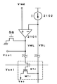
次に、読み出し動作について述べる。読み出し動作では、消去信号Seraseにはオフの信号が入力され、書込・読出信号Sw/rと読み出し信号Sreadにはオンの信号が入力される。その結果、メモリセル(1,1)への読み出し動作に関与する回路構成は、図21のように表すことができる。図21において、VWLはワード線の電位、VBLはビット線の電位、Vscは共通ソース線の電位、Vselは選択線の電位、Voutは出力される読み出し電位、Sdcはディスチャージ信号である。またオペアンプ2101には電位Vreadが入力され、定電流源2102からは定電流Iが供給される。図21に示した回路図は、選択トランジスタSTr、ディスチャージ回路及び読み出し電位Voutの出力部分を除いて、図1に示した回路図と一致し、その動作原理については既に説明を行った通りである。
【0111】
読み出し時の動作電圧としては、例えば、Sdc=0V、Vsel=5V、Vsc=GND、Vread=1V、I=1mAとすればよい。この場合のメモリトランジスタの動作点は、実施の形態で示した例(図11参照)とほぼ同様であると考えて良い。読み出し時の動作電圧としては、インパクトイオン化によってホットエレクトロンが発生しない条件とする必要がある。そのためには、Vreadを低く設定するとよい。
【0112】
そして、この動作電圧のもとで読み出し電位Voutを読み出すことによって、メモリセルに格納されているデータを読み出すことができる。この読み出し動作では、メモリトランジスタのしきい値電圧がΔVthだけ増加すると、制御回路1804(1)の負帰還の特性によってメモリトランジスタのコントロールゲート電圧、つまり読み出し電位VoutもΔVthだけ増加することを利用する。
【0113】
読み出し動作を行った後も、ディスチャージ動作によって全てのメモリトランジスタのコントロールゲート電極をGNDに落とす。まず、制御回路において、書込・読出信号Sw/rにオフの信号を入力すると共に、ディスチャージ信号Sdcにオンの信号を入力し、全てのワード線WLの電位をGNDに落とす。同時に全ての選択線SLの電位Vselを3Vとして、全てのメモリトランジスタのコントロールゲート電極をGNDに落とした後、全ての選択線SLの電位Vselを0Vに落とす。同時にディスチャージ信号Sdcにオフの信号を入力する。
【0114】
なお、読み出しを行わないメモリセル(2,1)〜(m,1)においては、選択線の電位Vselを0Vとして、選択トランジスタをオフとする。その結果、メモリセル(2,1)〜(m,1)を構成するメモリトランジスタはオフとなり、読み出し電位Voutはメモリセル(1,1)のみで決まるため、誤読み出しの心配は無い。また、動作電圧が低いために誤書き込みの問題も無い。一列目以外のメモリセルについても、制御回路1804(2)〜1804(n)が非選択の状態であり、ビット線とワード線がいずれも浮遊状態となっているために誤動作の問題はない。
【0115】
なお、本実施例では、読み出し方法としてワード線電位を読み出す方法を採用したが、ビット線電位を読み出す方法を用いることも可能である。
【0116】
最後に、消去動作について述べる。消去動作時には、消去信号Seraseにはオンの信号が入力され、書込・読出信号Sw/rと読み出し信号Sreadにはオフの信号が入力される。また、ディスチャージ信号Sdcにはオフの信号が入力される。その結果、メモリセル(1,1)〜(m,1)への消去動作に関与する回路構成は、図22のように表される。図22において、VWLはワード線の電位、Vscは共通ソース線の電位、Vsel(1)〜Vsel(m)は選択線の電位である。図22に示すように、消去動作においてはオペアンプおよび定電流源は関与しない。
【0117】
消去時の動作電圧としては、例えば、VWL=−8V、全ての選択線の電位Vsel(1)〜Vsel(m)を0V、および基板電位(またはウェル電位)を8Vとすればよい。その結果、一列目のメモリセルを構成する選択トランジスタはオンとなり、メモリトランジスタのコントロールゲート−基板間には16V程度の高い電位差が生じる。その結果、FNトンネル電流によってフローティングゲートに蓄積されていた電荷が基板へ引き抜かれる。なお、ビット線は浮遊状態となっている。一列目以外のメモリセルについては、制御回路1804(2)〜1804(n)が非選択の状態であり、ワード線が浮遊状態となっているために誤消去の問題はない。なお、基板電位を8Vとするかわりに、メモリトランジスタのソース領域とフローティングゲートとの間に一部重なる領域(オーバーラップ領域)を設けて、共通ソース電位Vscを8Vとすることも可能である。
【0118】
ベリファイを行わない書き込み動作後の分布幅を小さくするには、当然、書き込みを行う前しきい値電圧の分布幅が小さいことが必要である。しかしながら、上述した消去動作では、通常狭い分布幅を実現することは困難である。そこで、本実施例においては、FNトンネルによる消去動作の後に、新たに消去状態へのベリファイ書き込みを行うこととする。この消去状態のしきい値電圧は、0V以上であり、消去後の分布のよりもわずかに高い値とすることが好ましい。なお、消去状態へのベリファイ書き込みには、公知の回路構造と公知の動作方法を用いると良い。また、消去状態へのベリファイ書き込み後には、ディスチャージ動作によって、全てのメモリセルのコントロールゲートの電位を0Vとする。
【0119】
以上のようにして、本発明の不揮発性メモリの書き込み動作、読み出し動作および消去動作が行われる。
【0120】
本実施例では2値の不揮発性メモリについて述べたが、本発明の不揮発性メモリの特徴は高精度のしきい値制御性にあるから、むしろ、しきい値分布のマージンが少ない多値の不揮発性メモリにおいて特にその効果を発揮する。本実施例を実施例1と組み合わせることによって、書き込み時間の短い、また、多値度の高い不揮発性メモリを実現することが可能となる。
【0121】
なお、本実施例ではベリファイ動作を用いない書き込み方法について述べたが、もちろん、ベリファイ書き込みを行っても良い。また、本実施例ではメモリセル(1,1)への書き込みと読み出し及び一列目のメモリセル(1,1)〜(m,1)の一括消去の方法を述べたが、これらの動作を複数列に渡って同時に行うことも可能である。これらの応用については、実施の形態で説明を行った通りである。
【0122】
なお、本実施例では、消去状態におけるメモリトランジスタのしきい値電圧を正としたが、本発明はこの場合に限られるわけではない。消去状態におけるメモリトランジスタのしきい値電圧が負の場合には、ディスチャージ動作によって、コントロールゲートの電位を消去状態のしきい値電圧より低くすることによって、本実施例と全く同様に動作を行うことができる。この他、メモリトランジスタをスプリットゲート構造とすることも有効である。
【0123】
(実施例3)
本発明は、活性領域とコントロールゲート電極の間に電荷蓄積領域を有する様々なメモリ素子に対して適用することが可能である。特に、電化蓄積領域として半導体のクラスタ層、金属のクラスタ層、あるいは窒化膜を設けたメモリ素子に対しても適用することができる。これらのメモリ素子は、電荷を蓄積する領域が空間的に離散的に設けられていることを特徴とする
【0124】
電荷を蓄積する領域として半導体または導体のクラスタ層を用いるメモリ素子としては、例えば、特開昭49−22356号公報に開示されている。その代表的な断面構造を図26(a)に示す。図26(a)に示したメモリ素子は、活性領域2601上に、第1の絶縁膜2602と、クラスタ層2603と、第2の絶縁膜2605と、コントロールゲート電極2606とが順に積層されてなるメモリトランジスタである。クラスタ層2603は、離散的な塊状の半導体または導体(クラスタと呼ぶ)によって構成される層であり、この離散的なクラスタ2604が電荷の捕獲中心としての役割を果たす。
【0125】
また、電荷を蓄積する領域として窒化膜等を用いるメモリ素子としては、MNOS(Metal-Nitride-Oxide-Semiconductor)、MONOS(Metal-Oxide-Nitride-Oxide-Semiconductor)等が知られている。MNOS及びMONOSの代表的な断面構造を図26(b)及び(c)にそれぞれ示す。図26(b)示したメモリ素子は、活性領域上2607に、酸化膜2608、窒化膜2609、コントロールゲート電極2610が積層されてなる。また、図26(c)示したメモリ素子は、活性領域2611上に、酸化膜2612、窒化膜2613、酸化膜2614、コントロールゲート電極2615が積層されてなる。いずれにおいても、窒化膜中の空間的に離散的な不純物準位が電荷の捕獲中心としての役割を果たす。
【0126】
このようなメモリ素子を本発明の不揮発性メモリに応用する場合においても、実施の形態で説明を行った回路構成と動作方法をそのまま用いることができる。もちろん、動作電圧と動作電流はそれぞれの素子において最適な値を用いることが好ましい。
【0127】
メモリ素子として、電荷を蓄積する領域が離散的に設けられている素子を用いた場合、電荷保持特性がトンネル酸化膜の欠陥やピンホールの影響を受けにくいという効果がある。例えば、図26(d)に示すような、フローティングゲートを有するメモリトランジスタのように、電荷を蓄積する領域が連続的に設けられている場合には、トンネル酸化膜に一箇所のピンホールがあると、フローティングゲートに蓄積された電荷は全てそのピンホールからリークしてしまうため、メモリトランジスタの電荷保持特性に大きく影響する。しかし、電荷を蓄積する領域が離散的に設けられている素子を用いた場合には、ピンホールの影響を受ける領域は限定され、多くの電荷蓄積領域はそのピンホールの影響を受けないため、メモリ素子の電荷保持特性への影響は少ない。
【0128】
なお、フローティングゲートを有するメモリトランジスタとは、図26(d)に示すように、活性領域2616上に第1の絶縁膜2617と、半導体膜または導体膜によって構成されるフローティングゲート電極2618と、第2の絶縁膜2619と、コントロールゲート電極2620とが順に積層されてなるメモリトランジスタをいう。
【0129】
本実施例のメモリ素子を本発明の不揮発性メモリに応用する場合には、特に多値のメモリに応用することが好ましい。多値の不揮発性メモリは、異なる状態を表すしきい値電圧のマージンが少ないために、書き込み時や消去時における高精度のしきい値制御や、良好な電荷保持特性が必要となることは良く知られている。
そして、本発明の不揮発性メモリは、しきい値電圧の制御性に優れるために、多値の不揮発性メモリに対して特に有効であることは、実施の形態及び実施例1で述べた通りである。
【0130】
他方、多値の不揮発性メモリのもう一つの問題点である電荷保持特性については、本実施例のメモリ素子を用いることによって、大幅に改善することが可能となる。このように、本実施例で述べたメモリ素子は、本発明を多値の不揮発性メモリに応用する場合に特に好ましいということができる。
【0131】
なお、本実施例の構成は、実施例1、2のいずれの構成とも自由に組み合わせることが可能である。
【0132】
(実施例4)
本実施例では本発明の不揮発性メモリをワンチップ上に集積化されたRISCプロセッサ、ASICプロセッサ等のマイクロプロセッサに適用した場合の例について説明する。
【0133】
図23に示すのは、マイクロプロセッサの一例である。マイクロプロセッサは典型的にはCPUコア2301、フラッシュメモリ2304(RAMでも良い)、クロックコントローラ2303、キャッシュメモリ2302、キャッシュコントローラ2305、シリアルインターフェース2306、I/Oポート2307等から構成される。勿論、図23に示すマイクロプロセッサは簡略化した一例であり、実際のマイクロプロセッサはその用途によって多種多様な回路設計が行われる。
【0134】
図23に示すマイクロプロセッサではCPUコア2301、クロックコントローラ2303、キャッシュコントローラ2305、シリアルインターフェース2306、I/Oポート2307をCMOS回路で構成している。また、フラッシュメモリ2304には本発明の不揮発性メモリが用いられている。フラッシュメモリ2304としては、実施の形態及び実施例1〜3のいずれの構成とも組み合わせることが可能である。なお、キャッシュメモリ2302に本発明の不揮発性メモリを利用することも可能である。
【0135】
なお、本実施例のマイクロプロセッサは、実施例1〜3のどのような組み合わせからなる構成を用いても良い。
【0136】
(実施例5)
本発明の不揮発性メモリはデータの記憶・読み出しを行う記録媒体として、あらゆる分野の電子機器に組み込むことが可能である。本実施例では、その様な電子機器について説明する。
【0137】
本発明の不揮発性メモリを利用しうる電子機器としては、ディスプレイ、ビデオカメラ、デジタルカメラ、頭部取り付け型のディスプレイ、DVDプレーヤー、ゲーム機、ヘッドマウントディスプレイ(ゴーグル型ディスプレイ)、カーナビゲーション、音響再生装置(カーオーディオ等)、パーソナルコンピュータ、携帯情報端末(モバイルコンピュータ、携帯電話または電子書籍等)などが挙げられる。それらの一例を図24、25に示す。
【0138】
図24(A)はディスプレイであり、筐体2401、支持台2402、表示部2403等を含む。本発明は表示部2403やその他の信号制御回路に接続され、画像信号の補正や処理データの記憶に利用される。
【0139】
図24(B)はビデオカメラであり、本体2411、表示部2412、音声入力部2413、操作スイッチ2414、バッテリー2415、受像部2416で構成される。本発明は内蔵のLSI基板に組み込まれ、画像データの記憶などの機能に利用される。
【0140】
図24(C)は頭部取り付け型のディスプレイの一部(右片側)であり、本体2421、信号ケーブル2422、頭部固定バンド2423、表示部2424、光学系2425、表示装置2426等を含む。本発明は表示装置2426やその他の信号制御回路に接続され、画像信号の補正や処理データの記憶に利用される。
【0141】
図24(D)は記録媒体を備えた画像再生装置(具体的にはDVD再生装置)であり、本体2431、記録媒体2432、操作スイッチ2433、表示部2434、2435等で構成される。なお、この装置は記録媒体としてDVD(Digital Versatile Disc)、CD等を用い、音楽鑑賞や映画鑑賞やゲームやインターネットを行うことができる。本発明は内蔵のLSI基板に組み込まれ、画像データや処理データの記憶などの機能に利用される。
【0142】
図24(E)はゴーグル型ディスプレイ(ヘッドマウントディスプレイ)であり、本体2441、表示部2442、アーム部2443を含む。本発明は表示部2442やその他の信号制御回路に接続され、画像信号の補正や処理データの記憶に利用される。
【0143】
図24(F)はパーソナルコンピュータであり、本体2451、筐体2452、表示部2453、キーボード2454等で構成される。本発明は内蔵のLSI基板に組み込まれ、処理データや画像データの記憶に利用される。
【0144】
図25(A)は携帯電話であり、本体2501、音声出力部2502、音声入力部2503、表示部2504、操作スイッチ2505、アンテナ2506を含む。本発明は内蔵のLSI基板に組み込まれ、電話番号を記録するアドレス機能などを付加するために利用される。
【0145】
図25(B)は音響再生装置、具体的にはカーオーディオであり、本体2511、表示部2512、操作スイッチ2513、2514を含む。本発明は内蔵のLSI基板に組み込まれ、画像データや処理データの記憶などの機能に利用される。また、本実施例では車載用オーディオを示すが、携帯型や家庭用の音響再生装置に用いても良い。
【0146】
以上の様に、本発明の適用範囲は極めて広く、あらゆる分野の電子機器に適用することが可能である。また、本実施例の電子機器は実施例1〜3のどのような組み合わせからなる構成を用いても実現することができる。
【0147】
【発明の効果】
本発明の不揮発性メモリは、メモリ素子のドレイン電圧とドレイン電流とを制御することによって、書き込み動作において高精度のしきい値制御を行うことが可能となる。
【0148】
その結果、ベリファイ書き込みにおいてベリファイ回数を減らすこと、さらにはベリファイ方式を用いない書き込み方法が可能となり、従来と比較して書き込み時間の大幅な短縮を実現することが可能となる。
【0149】
本発明は、特に多値の不揮発性メモリに応用した場合に、書き込み時間短縮の効果は大きい。さらに、メモリ素子として、離散的な電荷蓄積領域を有するトランジスタを用いた場合には、電荷保持特性に優れ、書き込み時のしきい値制御性にも優れた多値の不揮発性メモリを提供することができる。
【0150】
本発明のしきい値制御性の優れた不揮発性メモリを搭載することによって、高速書き込み動作が可能な不揮発性メモリを具備する半導体装置を提供することができる。
【図面の簡単な説明】
【図1】 本発明の不揮発性メモリの書き込み動作を説明する回路図。
【図2】 本発明の不揮発性メモリのしきい値電圧と書き込み時間の関係を示す図。
【図3】 本発明の不揮発性メモリの書き込み動作後のしきい値分布を表す図。
【図4】 本発明の不揮発性メモリの全体構成を示す図。
【図5】 本発明の不揮発性メモリの部分構成を示す図。
【図6】 本発明の不揮発性メモリの部分構成を示す図。
【図7】 本発明の不揮発性メモリの部分構成を示す図。
【図8】 本発明の不揮発性メモリの書き込み動作を説明する回路図。
【図9】 本発明の不揮発性メモリの書き込み時の動作点を示す図。
【図10】 本発明の不揮発性メモリの読み出し動作を説明する回路図。
【図11】 本発明の不揮発性メモリの読み出し時の動作点を示す図。
【図12】 本発明の不揮発性メモリの消去動作を説明する回路図。
【図13】 本発明の不揮発性メモリのしきい値分布を表す図。
【図14】 本発明の不揮発性メモリのしきい値電圧と書き込み時間の関係を示す図。
【図15】 本発明の不揮発性メモリの書き込み回路図。
【図16】 本発明の不揮発性メモリの書き込み時のタイミングチャート。
【図17】 本発明の不揮発性メモリの書き込み回路図。
【図18】 本発明の不揮発性メモリの全体構成を示す図。
【図19】 本発明の不揮発性メモリの部分構成を示す図。
【図20】 本発明の不揮発性メモリの書き込み動作を説明する回路図。
【図21】 本発明の不揮発性メモリの読み出し動作を説明する回路図。
【図22】 本発明の不揮発性メモリの消去動作を説明する回路図。
【図23】 本発明の不揮発性メモリを用いた半導体回路を示す図。
【図24】 本発明の不揮発性メモリを用いた電子機器を示す図。
【図25】 本発明の不揮発性メモリを用いた電子機器を示す図。
【図26】 本発明の不揮発性メモリを構成するメモリ素子の断面図。
【符号の説明】
101 メモリトランジスタ
102 定電流源
103 オペアンプ[0001]
[Technical field to which the invention belongs]
The present invention relates to a semiconductor nonvolatile memory. In particular, the present invention relates to an electrically writable and erasable semiconductor nonvolatile memory (also referred to as EEPROM or Electrically Erasable and Programmable Read Only Memory). The present invention is particularly effective for a semiconductor nonvolatile memory using a multi-value technology. The present invention also relates to a semiconductor device including a semiconductor nonvolatile memory.
[0002]
In this specification, an electrically writable and erasable semiconductor non-volatile memory (EEPROM) literally refers to an entire semiconductor non-volatile memory capable of electrical writing and erasing, for example, a full-function EEPROM, Or the flash memory is included in the category. Unless otherwise specified, the nonvolatile memory and the semiconductor nonvolatile memory are used synonymously with the EEPROM. A semiconductor device refers to all devices that function by utilizing semiconductor characteristics, and includes, for example, an electro-optical device typified by a microprocessor, a liquid crystal display device, and a light-emitting device, and a microprocessor or an electro-optical device. Electronic equipment is included in the category.
[0003]
[Prior art]
In recent years, an electrically writable and erasable semiconductor non-volatile memory (EEPROM), particularly a flash memory, has attracted attention as a promising candidate for replacing a magnetic disk or DRAM. In particular, a so-called multi-value nonvolatile memory in which individual memory elements store three or more values is drawing attention as a large-capacity memory.
[0004]
Nonvolatile memories are classified into NOR type, NAND type, AND type, and DINOR type depending on the circuit configuration and operation method. Further, as a memory element constituting the nonvolatile memory, a memory transistor having a floating gate, a memory transistor having a cluster layer, a MNOS (Metal-Nitride-Oxide-Semiconductor) structure or a MONOS (Metal-Oxide-Nitride-Oxide-Semiconductor) A memory transistor having a structure is known.
[0005]
In a conventional nonvolatile memory, a typical write operation includes a hot electron injection method (referred to as an HE injection method) and a charge injection method using an FN tunnel current (referred to as an FN current method). In the HE injection method, a high control gate voltage and a high drain voltage are applied to the memory transistor to cause impact ionization, and electric charges are injected into the memory transistor by drawing the generated hot electrons to the gate electrode side. On the other hand, in the FN current method, charges are injected into the memory transistor by applying a high voltage between the control gate electrode and the substrate to flow an FN tunnel current.
[0006]
In either case, verify writing is usually performed to confirm that the threshold voltage after writing is within a predetermined range. In particular, in a multi-value nonvolatile memory, verify writing is indispensable because it is necessary to control the threshold voltage after writing with high accuracy. The verify writing is a method of alternately performing a small amount of charge injection and reading for confirming the threshold voltage. This operation is repeated until the threshold voltage after writing falls within a predetermined range.
[0007]
[Problems to be solved by the invention]
The above-described charge injection method has a problem that it is difficult to accurately control the charge injection amount. This is because even when the same operating voltage is applied to the memory transistor, the charge injection rate differs if the charge accumulation amount of the memory transistor, that is, the threshold voltage is different.
[0008]
Therefore, the charge injection speed changes with time even for the same memory transistor as well as memory transistors with different threshold voltages. For example, when electrons are injected, the threshold voltage increases, and the effective gate voltage viewed from the channel region decreases, so the charge injection rate decreases.
[0009]
Furthermore, if the charge injection rate varies due to factors such as variations in the quality of the tunnel oxide film, even if the threshold voltage of the memory transistor before writing is equal, there will be a difference in the amount of accumulated charge. When a difference occurs in the threshold voltage, a vicious cycle occurs in which the charge injection amount further varies.
[0010]
Verify writing is one method for solving such a problem. In verify writing, the threshold voltage is checked every time a small amount of charge is injected, so that it is not necessary to control the amount of charge injection with high accuracy. However, the verify write has a problem that it essentially takes time to divide the charge injection operation and perform the read operation during that time.
[0011]
It should be noted that it is important to accurately control the amount of charge injection in verify writing. By controlling the charge injection amount with high accuracy, the division of the charge injection operation can be reduced, and the verify write time can be shortened.
[0012]
The present invention has been made in view of the above problems. It is an object of the present invention to provide a non-volatile memory that performs a write operation that can control the charge injection amount with high accuracy. It is another object of the present invention to provide a non-volatile memory that achieves a significant reduction in write time by shortening the verify write time, and further by a write method that does not use the verify method. It is another object of the present invention to provide a semiconductor device including such a nonvolatile memory.
[0013]
[Means for Solving the Problems]
As already described, in the conventional writing method, the charge injection speed depends on the charge accumulation amount of the memory transistor, and hence the threshold voltage. As a result, not only the memory transistors in different states but also the same memory transistor, the charge injection speed changes with time, and it is difficult to control the charge injection amount.
[0014]
This means that, in order to control the charge injection amount with high accuracy, a writing method having a charge injection rate that does not depend on the charge accumulation amount of the memory transistor, that is, the threshold voltage, is effective. The present inventor considers that the charge injection speed depends on the threshold voltage of the memory transistor because it directly controls the control gate voltage of the memory transistor at the time of writing. A method to control voltage and drain current was devised.
[0015]
That is, the nonvolatile memory of the present invention is characterized in that a hot electron injection type write operation is performed by controlling the drain voltage and drain current of the memory transistor. This writing method does not directly control the control gate voltage, but indirectly controls the control gate voltage so that the drain current is constant, and the charge injection speed does not depend on the threshold voltage. It is characterized by.
[0016]
In order to understand the write operation in the nonvolatile memory of the present invention, the operation method will be described by taking a simple circuit for writing to one memory element as an example. For description, FIG. 1 (a) or (b) is used.
[0017]
As the memory element, various elements as shown in FIG. 26 can be used (refer to Example 3 for details). In FIG. 26A, a first insulating film 2602, a cluster layer 2603 composed of a semiconductor or
[0018]
Here, an example of a circuit diagram using a memory transistor having a cluster layer, a memory transistor having an MNOS structure, or a memory transistor having a MONOS structure as the memory element is shown in FIG. 1A, and a memory transistor having a floating gate is used. An example of the circuit diagram is shown in FIG. As symbolized by each memory element, the memory transistor shown in FIG. 1A is characterized in that the regions for storing charges are spatially discrete, and the memory shown in FIG. The transistor is characterized in that a region for accumulating charges is continuous. In any case, the operation method is exactly the same, and here, description will be made with reference to FIG.
[0019]
The circuit diagram shown in FIG. 1A includes a memory transistor 101 (a), a constant current source 102 that supplies a current amount I, and an operational amplifier 103. The output of the operational amplifier 103 is connected to the control gate electrode of the memory transistor 101 (a), the constant current source 102 is connected to the drain electrode, and the source electrode is grounded. The constant current source 102 and the voltage Vpgm are connected to the two input terminals of the operational amplifier 103, respectively.
[0020]
The circuit shown in FIG. 1 has a negative feedback characteristic, and the two potentials input to the operational amplifier 103 always operate in the same state. As a result, in the circuit diagram shown in FIG. 1, the memory transistor 101 (a) operates in a state where the drain voltage is equal to Vpgm and the drain current is equal to I.
[0021]
Actually, when the drain voltage of the memory transistor 101 (a) is higher than Vpgm, a positive current is output from the operational amplifier 103, and the control gate voltage of the memory transistor 101 (a) increases. As a result, the conductance of the memory transistor 101 (a) increases and the drain voltage is lowered. Conversely, when the drain voltage of the memory transistor 101 (a) is lower than Vpgm, a negative current is output from the operational amplifier 103, and the control gate voltage of the memory transistor 101 (a) decreases. As a result, it can be seen that the conductance of the memory transistor 101 (a) decreases and the drain voltage is raised.
[0022]
In the present invention, the write operation of the HE injection method is performed by controlling the drain voltage and drain current of the memory transistor as described above. Vpgm is called a write voltage, and I is called a write current.
[0023]
When the above-described writing method is used and the drain voltage and the drain current are constant, the channel region of the memory transistor assumes the same state regardless of the charge accumulation amount of the floating gate. That is, the control gate voltage is shifted by the same amount as the shift of the threshold voltage, and the effective gate voltage viewed from the channel region is always kept constant. Furthermore, if the drain voltage and the drain current are constant, a certain amount of hot electrons are generated, so that the rate of charge injection into the floating gate is constant.
[0024]
This means that when the write voltage Vpgm and the write current I are constant, the threshold voltage shift ΔVth of the memory transistor and the write time tw are represented by a straight line as shown by a
[0025]
FIG. 2 also shows the relationship between the threshold voltage shift and the writing time in the conventional writing method (
[0026]
In the present invention, the charge injection speed at the time of writing can be optimized by setting the drain voltage and drain current of the memory transistor to appropriate values. Since the writing method in the present invention is hot electron injection, the drain voltage needs to be large enough to generate hot electrons. On the other hand, if a large amount of hot electrons are generated, the controllability of the charge injection amount is lowered, so that it is not preferable that the drain voltage is too large. Although the drain voltage of the memory transistor depends on the size of the memory transistor, it is preferably 3 V or more, and preferably operates in a saturation region relatively close to the linear region. Further, in such a region, the write speed is improved by setting the write voltage Vpgm and the write current I to a large value, and conversely, the current consumption can be suppressed by setting the write voltage Vpgm and the write current I to a small value. The write voltage Vpgm and the write current I may be set to optimum operating points according to the use of the nonvolatile memory.
[0027]
In addition, since the above-described writing method is a hot electron injection method, electrons having energy much higher than the energy barrier by the tunnel oxide film are mainly involved. For this reason, variations in the quality of the tunnel oxide film hardly affect the injection amount of hot electrons, and threshold control can be performed with less variation compared to the charge injection method using the FN tunnel current.
[0028]
The nonvolatile memory of the present invention can significantly reduce the writing time as follows by using the above-described writing operation.
[0029]
First, referring to FIG. FIG. 3 qualitatively shows the threshold distribution after the conventional writing and the writing according to the present invention are performed without verify operation on the memory transistors having the same threshold voltage. A distribution 302 represents a threshold voltage distribution after writing in the related art, and a distribution 301 represents a threshold voltage distribution after writing in the present invention. Vtar is a set threshold voltage after writing. In FIG. 3, when the distribution 302 after writing in the present invention is compared with the distribution 301 after writing, the deviation between the center of the distribution and Vtar and the distribution width are both small (ΔV <ΔV ′ and δv). <Δv ′).
[0030]
In general, when the difference between threshold voltages representing different states is small compared to the distribution width and center shift after writing, all memory cells cannot be brought into a predetermined state by one writing. Verify writing is required. On the other hand, when the difference in threshold voltage is larger than the distribution width and center shift after writing, writing can be performed by a single writing operation. Note that verify writing refers to a method in which writing is not performed at a time, but a small amount of writing and reading for checking a threshold value are alternately performed. This operation is repeated until a predetermined threshold is reached.
[0031]
In the conventional writing method, as shown in FIG. 3, since the distribution width δv ′ and the center deviation ΔV ′ after writing are large, the verify writing method is usually used.
[0032]
When the writing method according to the present invention is used, since the distribution width δv and the center shift ΔV after writing are small as shown in FIG. 3, the threshold value at which the verify operation is necessary in the conventional writing method. Even with a voltage difference, a write operation without performing a verify operation can be performed. Specifically, when the difference in threshold voltage between different states is larger than the threshold voltage distribution width δv and the center shift ΔV after writing in the present invention, a writing operation without performing a verify operation becomes possible. .
[0033]
Further, when the difference in threshold voltages representing different states is small as in a multi-value nonvolatile memory, a verify operation is required even when the write method according to the present invention is used. In this case, the write operation may be configured by a first write operation in which the verify operation is not performed and a second write operation in which the verify operation is performed. Specifically, first, writing to a state slightly lower than the final threshold voltage (about δv or ΔV) is performed by the first writing operation, and then the remaining threshold voltage deficiency (δv or Verify write is performed for about ΔV. Since the amount of data written in the second write operation is very small, the number of verify operations can be greatly reduced as compared with the conventional verify write.
[0034]
As described above, when the write method according to the present invention is used, the number of verify operations can be reduced and the write time can be greatly shortened not only in the write operation without verify but also in the write operation in which verify is performed. .
[0035]
Further, in the conventional writing method, as shown in FIG. 2, when the threshold voltage increases, the charge injection speed decreases and the writing operation becomes slow. However, in the writing method according to the present invention, even at a high threshold voltage. The charge injection speed is constant, and a high-speed write operation is possible.
[0036]
The configuration of the present invention is shown below.
[0037]
In an electrically writable and erasable nonvolatile memory constituted by a memory element having a charge storage region between an active region and a control gate electrode, the amount of current flowing through the memory element and the drain voltage of the memory element are controlled Thus, a nonvolatile memory is provided that controls the amount of charge injected into the charge storage region.
[0038]
In an electrically writable and erasable nonvolatile memory configured by a memory element having a charge storage region between an active region and a control gate electrode, charge injection into the charge storage region is caused by an amount of current flowing through the memory element. And a drain voltage of the memory element, and a charge injection amount into the charge storage region is controlled by controlling a time during which a current flows through the memory element. Provided.
[0039]
An electrically writable and erasable non-volatile memory having a memory cell in which a plurality of memory cells are arranged in a matrix and a writing circuit, each of the memory cells having a memory element and a selection transistor The memory device has a charge storage region between an active region and a control gate electrode, and the write circuit performs a write operation by controlling an amount of current flowing through the memory device and a drain voltage of the memory device. A non-volatile memory is provided that is characterized in that it does.
[0040]
An electrically writable and erasable non-volatile memory having a memory cell in which a plurality of memory cells are arranged in a matrix and a writing circuit, each of the memory cells having a memory element and a selection transistor The memory element has a charge storage region between an active region and a control gate electrode, and the write circuit has a function of maintaining a constant amount of current flowing through the memory element and a drain voltage of the memory element. The write circuit performs a write operation by controlling a time during which a current amount flowing through the memory element and a drain voltage of the memory element are kept constant.
[0041]
An electrically writable and erasable non-volatile memory having a memory cell in which a plurality of memory cells are arranged in a matrix and a writing circuit, each of the memory cells having a memory element and a selection transistor The memory element has a charge storage region between the active region and the control gate electrode, and the memory element has a k-value state of two or more values, an erased state having a threshold voltage Vth0, and Memory is stored in a state having (k−1) different threshold voltages Vth1, Vth2,..., Vth (k−1) higher than that in the erased state, and the write circuit A function of maintaining a constant drain voltage of the memory element, and the write circuit includes a current amount flowing through the memory element and a drain current of the memory element. And write time tw1, tw2, from the erased state to the state having the threshold voltages Vth1, Vth2,..., Vth (k-1). The ratio of tw (k-1) is tw1: tw2:-: tw (k-1) = (Vth1-Vth0) :( Vth2-Vth0):-:( Vth (k-1) -Vth0). A non-volatile memory is provided.
[0042]
The memory element may store multi-value data.
[0043]
The nonvolatile memory may perform a read operation by reading a gate voltage of the memory element.
[0044]
The verify operation may not be performed in the write operation of the nonvolatile memory.
[0045]
The write operation of the non-volatile memory includes a first write operation and a second write operation. The verify operation may not be performed in the first write operation, and the verify operation may be performed in the second write operation.
[0046]
In the memory element constituting the nonvolatile memory, a first insulating film, a floating gate electrode formed of a semiconductor film or a conductor film, a second insulating film, and a control gate electrode are sequentially stacked on the active region. It may be a memory transistor.
[0047]
The memory element constituting the nonvolatile memory includes a first insulating film on the active region, a cluster layer having a cluster made of a semiconductor or a conductor as a charge trapping center inside the insulator, a second insulating film, It may be a memory transistor in which a control gate electrode is sequentially stacked.
[0048]
The memory element constituting the nonvolatile memory may be a memory transistor having an MNOS structure or a MONOS structure.
[0049]
A semiconductor device using the nonvolatile memory as a recording medium is provided.
[0050]
A microprocessor is provided as the semiconductor device.
[0051]
As the semiconductor device, a display, a video camera, a head mounted display, a DVD player, a head mounted display, a personal computer, a mobile phone, and a car audio are provided.
[0052]
DETAILED DESCRIPTION OF THE INVENTION
In this embodiment mode, a circuit configuration and an operation method of a nonvolatile memory that performs the above-described write operation will be described. Here, for the sake of simplicity, a case of a binary nonvolatile memory and a writing method in which a verify operation is not performed will be described. However, the present invention is also applicable to a multi-value nonvolatile memory and a verify write. It is easy to apply the embodiment.
[0053]
FIG. 4 shows an example of a circuit diagram of a nonvolatile memory of the present invention having a memory cell array of m rows and n columns (m and n are each an integer of 1 or more). The nonvolatile memory shown in FIG. 4 includes a memory cell array 401, an X address decoder 402, a Y address decoder 403, control circuits 404 (1) to 404 (n), a read / write circuit 405, and other peripheral circuits (not shown). Z). Other peripheral circuits include an address buffer circuit, a power supply generation circuit, a booster circuit, a power supply control circuit, other control circuits, and the like, and are provided as necessary.
[0054]
Note that in this specification, the writing circuit refers to the entire circuit related to the writing operation, but only a part related to the writing operation may be extracted and referred to as a writing circuit. For example, in the circuit diagram of the nonvolatile memory shown in FIG. 4, the write circuit refers to the entire circuit involved in the write operation including the write / read circuit 405 and the
[0055]
In the nonvolatile memory according to the present embodiment, each memory cell includes a memory transistor MTr and a selection transistor STr. The memory transistor MTr is a memory transistor having a floating gate (see the third embodiment), and the selection transistor STr is a normal transistor. As the memory transistor MTr, a memory element in which charge storage regions are spatially discrete, such as a memory transistor having a cluster layer, a memory transistor having an MNOS structure or a MONOS structure, can be used (Example 3). ). When each memory cell stores 1-bit data, the nonvolatile memory according to the present embodiment has a storage capacity of m × n bits.
[0056]
In FIG. 4, a memory cell (i, j) (1 ≦ i ≦ m, 1 ≦ j ≦ n) is connected to a selection line SLi, a word line WLj, a bit line BLj, and a common source line SC. Specifically, the word line WLj is connected to the control gate electrode of the memory transistor MTr, the common source line SC is connected to the source electrode, the selection line SLi is connected to the gate electrode of the selection transistor STr, and the bit line is connected to the drain electrode. BLi is connected. Further, the memory transistor MTr and the selection transistor STr constituting the memory cell (i, j) are connected in series. The selection lines SL1 to SLm are connected to the coder 403 with a Y address, and the word line WLj and the bit line BLj are connected to the control circuit 404 (j) (1 ≦ j ≦ n). The control circuits 404 (1) to 404 (n) are connected to the X address decoder 402 and the read / write circuit 405.
[0057]
Next, the control circuits 404 (1) to (n) will be described. Since all n control circuits are the same, hereinafter, one of them will be represented as a
[0058]
The
[0059]
As the
[0060]
Next, an operation method of the nonvolatile memory according to this embodiment is described. Here, writing to and reading from the memory cell (1, 1) and batch erase of the memory cells (1, 1) to (1, m) in the first column will be described. Of course, the same operation can be performed for other memory cells. Note that in this embodiment mode, a case where each memory transistor stores binary data and a verify operation is not performed at the time of writing will be described.
[0061]
First, before each operation is performed, the memory cells in the first column are selected by the X address decoder. Specifically, the
[0062]
In the write operation, all the
[0063]
For example, Vsel = 10V, Vsc = GND, Vpgm = 6V, and I = 10 mA may be used as the operating voltage at the time of writing. The operating point of the memory transistor in this case is shown in FIG.
[0064]
With the above-described writing method, a writing operation with a constant charge injection speed into the memory cell (1, 1) can be performed. In this embodiment, the memory transistor stores 1-bit information (binary value of “0” or “1”). When writing “0”, nothing is done, and when writing “1” Performs the above-described write operation only for time tw. It is assumed that the write operation is performed for a state in which the threshold voltages Vth are well aligned. The time tw is the writing time required to obtain the “1” state, and is checked in advance. In this embodiment, since the verify operation is not performed and only the write operation at time tw is performed, the write time can be greatly shortened as compared with the conventional verify write. Of course, such a write operation is possible because a threshold distribution with high accuracy and a small distribution width can be obtained by the write method of the present invention.
[0065]
Note that in the memory cells (2, 1) to (m, 1) where writing is not performed, the potential Vsel of the selection line is set to 0 V, and the selection transistor is turned off. Further, it is necessary to set the operating voltage at the time of writing so that the potential VWL of the word line at the time of writing is such that erroneous writing due to the tunnel current is not performed in the memory cells (2, 1) to (m, 1). is there. In addition, regarding the memory cells other than the first column, the control circuits 404 (2) to 404 (n) are in a non-selected state, and both the bit line and the word line are in a floating state. Absent.
[0066]
Next, a read operation will be described. In the read operation, an off signal is input to the erase signal Serase, and an on signal is input to the write / read signal Sw / r and the read signal Sread. As a result, the circuit configuration involved in the read operation to the memory cell (1, 1) can be expressed as shown in FIG. In FIG. 10, VWL is a word line potential, VBL is a bit line potential, Vsc is a common source line potential, Vsel is a selection line potential, and Vout is an output read potential. The
[0067]
For example, Vsel = 3V, Vsc = GND, Vread = 1V, and I = 1 mA may be used as read operation voltages. The operating point of the memory transistor in this case is shown in FIG.
[0068]
Then, the data stored in the memory cell can be read by reading the read potential Vout under this operating voltage. In this read operation, when the threshold voltage of the memory transistor MTr increases by ΔVth, the control gate voltage of the memory transistor MTr, that is, the read potential Vout increases by ΔVth due to the negative feedback characteristic of the control circuit 404 (1). Use.
[0069]
Note that in the memory cells (2, 1) to (m, 1) that are not read, the potential Vsel of the selection line is set to 0 V, and the selection transistor is turned off. As a result, the read potential Vout is determined only by the memory cell (1, 1), and there is no fear of erroneous reading. Further, since the operating voltage is low, there is no problem of erroneous writing. Also in the memory cells other than the first column, the control circuits 404 (2) to 404 (n) are in a non-selected state, and both the bit line and the word line are in a floating state, so there is no problem of malfunction.
[0070]
Note that although a method of reading a word line potential is used as a reading method in this embodiment mode, a method of reading a bit line potential can also be used.
[0071]
Finally, the erase operation will be described. During the erase operation, an ON signal is input to the erase signal Serase, and an OFF signal is input to the write / read signal Sw / r and the read signal Sread. As a result, the circuit configuration involved in the erase operation to the memory cells (1, 1) to (m, 1) is expressed as shown in FIG. In FIG. 12, VWL is the potential of the word line, Vsc is the potential of the common source line, and Vsel (1) to Vsel (m) are the potentials of the selection lines. As shown in FIG. 12, the operational amplifier and the constant current source are not involved in the erase operation.
[0072]
As the operating voltage at the time of erasing, for example, VWL = −8V, the potentials Vsel (1) to Vsel (m) of all the selection lines may be 0V, and the substrate potential (or well potential) may be 8V. As a result, a high potential difference is generated between the control gate and the substrate of the memory transistors constituting the memory cells in the first column, and the charges accumulated in the floating gate are extracted to the substrate by the FN tunnel current. Note that the selection transistor is off and the drain region of the memory transistor is in a floating state. Further, for the memory cells other than the first column, the control circuits 404 (2) to 404 (n) are in a non-selected state, and the word line is in a floating state, so there is no problem of erroneous erasure. Instead of setting the substrate potential to 8V, it is also possible to provide a partially overlapping region (overlap region) between the source region of the memory transistor and the floating gate so that the common source potential Vsc is 8V.
[0073]
In order to reduce the distribution width after the write operation without verifying, it is naturally necessary that the distribution width of the threshold voltage before writing is small. However, in the erase operation described above, it is usually difficult to realize a narrow distribution width. Therefore, in this embodiment, after the erase operation by the FN tunnel, verify write to the erase state is newly performed. The threshold voltage in the erased state is preferably set to a value slightly higher than the distribution after erasure. Note that a known circuit structure and a known operation method may be used for the verify write to the erased state.
[0074]
As described above, the write operation, read operation, and erase operation of the nonvolatile memory of the present invention are performed. The operating voltages described in this embodiment are summarized as shown in Table 1. In Table 1, the operating voltage when the charge is extracted to the source region as an erasing method is written.
[0075]
[Table 1]
In this embodiment mode, a binary nonvolatile memory has been described. However, the present invention is not limited to binary nonvolatile memories. Rather, the non-volatile memory of the present invention is characterized by high-precision threshold controllability, and thus is particularly effective in a multi-level non-volatile memory having a small threshold distribution margin. By applying the present invention to a multi-value nonvolatile memory, the writing time can be shortened compared to the conventional case, and a high multi-value can be realized.
[0077]
In this embodiment, the writing method that does not use the verify operation has been described. Of course, a write method that uses the verify operation may be performed. In that case, the write operation may be configured by a first write operation in which the verify operation is not performed and a second write operation in which the verify operation is performed. Specifically, first, in the first write operation, writing to a state slightly lower than the final threshold voltage is performed using the highly accurate threshold control characteristic, and then the remaining threshold value is stored. It is preferable to perform verify writing for the shortage of voltage. As a result, the number of verify operations can be reduced as compared with the conventional verify write, and the time for verify write can be shortened. Note that for the verify write, a known circuit structure and a known operation method may be used.
[0078]
In this embodiment, the method of writing to and reading from the memory cell (1, 1) and the method of batch erasing the memory cells (1, 1) to (m, 1) in the first column are described. It is also possible to carry out simultaneously over a plurality of columns. In particular, by selecting all of the control circuits 404 (1) to 404 (n), simultaneous writing and reading to the memory cells (1, 1) to (1, n) in the first row, and all of the memory cells It is possible to perform batch erasure. Of course, the write / read circuit 405 requires a circuit that can handle n-bit data in parallel. Further, it is necessary that the total amount of current flowing simultaneously in each operation does not exceed the current drive capability of the circuit.
[0079]
In the writing method according to the present invention, since negative feedback is used, it may take time until the operating voltage is stabilized. For this reason, it is preferable to provide a discharge circuit or a precharge circuit in the control circuit as necessary to shorten the time until the operating voltage is stabilized.
[0080]
Example 1
In this embodiment, an example in which the nonvolatile memory of the present invention is applied to multiple values will be described.
The nonvolatile memory of the present invention is characterized by a write operation with excellent controllability of threshold voltage, and is particularly effective in a multi-value nonvolatile memory with a small threshold distribution margin. The multi-value nonvolatile memory to which the present invention is applied can shorten the writing time as compared with the conventional one, and can realize a high multi-value degree.
[0081]
A multi-value nonvolatile memory is constituted by a memory element that can store three or more states. For example, there are a method of distinguishing the threshold voltage of a memory element into three or more states, a method of using a memory element that can store charges in a plurality of locations, and the like. In this embodiment, the threshold voltage of the memory element is classified into four states, and a four-value nonvolatile memory for storing four states of “0” (erased state), “1”, “2”, and “3”. The memory will be described. FIG. 13 shows threshold voltage distributions representing four states. In FIG. 13, Vth0, Vth1, Vth2, and Vth3 are values at the centers of threshold distributions of states “0”, “1”, “2”, and “3”, respectively.
[0082]
FIG. 14 shows the relationship between the threshold voltage of the memory element and the writing time when the writing method of the present invention is used. In FIG. 14, times tw1, tw2, and tw3 represent write times from the erased state “0” to “1”, “2”, and “3”, respectively. Since the threshold voltage and the writing time have a linear relationship, when the intervals of the threshold voltages of the four states are equal, the ratio of tw1, tw2, tw3 is tw1: tw2: tw3 = 1: 2: 3. It becomes. As described above, in the writing method of the present invention, writing to each state can be performed easily and with high accuracy by controlling the writing time. More generally, when writing is performed by a single writing operation, the ratio of the required writing times may be made to coincide with the ratio of the threshold voltage intervals in each state.
[0083]
The circuit configuration and operation method of the quaternary nonvolatile memory of the present invention will be described below. For simplicity, it is assumed that threshold distributions representing four-value states are as shown in FIG. 13, and the intervals of the threshold voltages in each state are equal.
[0084]
The circuit configuration of the multi-value nonvolatile memory may be basically the same as that of the binary nonvolatile memory. The memory cell array, address decoder, control circuit, and the like are the same as the circuit diagrams shown in FIGS. The same can be used. The difference between the multi-value circuit configuration and the binary case is mainly a read circuit and a write circuit. In a quaternary nonvolatile memory, it is necessary that the read circuit distinguishes four states and reads them as 2-bit data, and the write circuit writes to the four states based on the 2-bit data. Accordingly, the read circuit and the write circuit are different for each non-volatile memory (including binary) having different multivalue levels.
[0085]
As a writing method, a single writing operation without performing a verify operation is considered.
In this case, a write operation in which the write time is 0, tw1, tw2, or tw3 may be performed based on the input 2-bit data. The writing operation may be the same as the method described in the embodiment, and an ON pulse signal having a width of 0, tw1, tw2, or tw3 may be input to the write / read signal. Of course, it is desirable to use an optimum value determined by the writing time or the like for the operating voltage. In the writing method according to the present invention, since the charge injection speed is constant, writing can be performed by simple time control in which the ratio of the writing time to the four states is 0: 1: 2: 3.
[0086]
As a reading method, first, the reading potential Vout is read from the control circuit in the same manner as the binary memory. In the reading circuit, the states “0”, “1”, “2”, and “3” may be determined based on the read value of Vout and converted into 2-bit data. As the readout circuit, a known readout circuit used in a conventional multi-value nonvolatile memory can be used.
[0087]
As the erasing method, erasing to “0” (erasing state) may be performed regardless of the state of the memory element. Therefore, the erasing operation by the FN tunnel current may be performed as in the binary memory. Note that when the verify operation is not performed in the write operation, the threshold voltages before the write operation need to be made uniform. Therefore, as described in the embodiment, after the FN tunnel erase operation, the erase state “0” is obtained. It is preferable to perform verify writing to the memory. For verify write to the erased state “0”, a known circuit configuration and a known operation method may be used.
[0088]
An example of the write operation will be described in more detail. FIG. 15 shows an example of a write circuit diagram. The write circuit 1501 includes a latch 1502, a pulse generation circuit 1503, and the like. When 2-bit write data is input to the write circuit 1501, it is held in the latch 1502 and a plurality of signals are formed by the pulse generation circuit 1503. These signals are appropriately selected according to the data held in the latch 1502, and are output as the write pulse signal Sw and the write end signal Swf.
[0089]
FIG. 16 shows a timing chart of the write pulse signal Sw and the write end signal Swf. As shown in FIG. 16, the write pulse signal Sw has a different pulse width based on the input data, and the write end signal Swf rises after the write pulse falls to transmit the write end. Specifically, when data corresponding to states “0”, “1”, “2”, and “3” is input, the write signal Sw has pulse widths of 0, tw1, tw2, and tw3, respectively. Have.
[0090]
The output write pulse signal Sw is connected to a switch transistor that switches connection between the input terminal of the operational amplifier and Vpgm and GND. When the write pulse signal Sw is on, Vpgm is connected to the input terminal of the operational amplifier, and when it is off, GND is connected to the input terminal of the operational amplifier.
[0091]
In the above-described pulse generation circuit 1503, for example, three rising signals shifted in time by tw1, tw2 and tw3 are generated by a shift register, and an exclusive OR (XOR) with the original signal is taken to obtain a width. Different pulses can be created. The write pulse signal Sw may be selected from pulse signals having different widths, and the write end signal Swf may be selected from rising signals shifted in time based on input data.
[0092]
As described above, the write operation, read operation, and erase operation of the nonvolatile memory of the present invention are performed.
[0093]
In this embodiment, the case of four values has been described on behalf of the multi-value memory. However, the present invention is also applied to a multi-value memory having eight values, sixteen values, or more in the same manner as this embodiment. Can be applied. In this embodiment, the case where the intervals of the threshold distribution representing the multi-valued state are uniform is described. However, the write pulse width can be obtained even when the intervals of the threshold distribution representing the multi-valued state are not uniform. It is possible to perform exactly the same operation only by changing.
[0094]
In the write operation according to the present invention, the threshold voltage distribution width after write is smaller than in the conventional case, and the distribution controllability is excellent. Therefore, even in a multi-value nonvolatile memory, the write operation is not performed once. It may be possible to perform writing by operation. Even in the case of performing the verify operation, first, writing to a state where the threshold voltage is slightly lower than the state after writing (first writing) is performed, and then verify writing (second writing) is performed. Thus, the writing time can be greatly shortened. The verify write may be started by confirming the rising edge of the write end signal Swf. Although the verify write circuit is not shown, a known circuit structure and a known operation method may be used.
[0095]
Further, the above-described operation method of the multi-level memory can be performed simultaneously over a plurality of columns. In that case, a writing circuit diagram as shown in FIG. 17 can be used. In FIG. 17, a
[0096]
As a method for controlling the threshold voltage with high accuracy, the control method based on the time as described above is preferable, but more generally, the write voltage Vpgm and the write time are freely set, and a multi-value is controlled. A write operation to each state may be performed.
[0097]
(Example 2)
In this example, an example different from the circuit configuration of the nonvolatile memory described in the embodiment will be described. FIG. 18 shows a circuit diagram of the nonvolatile memory of this embodiment having a memory cell array of m rows and n columns (m and n are each an integer of 1 or more). The nonvolatile memory shown in FIG. 18 includes a memory cell array 1801, an X address decoder 1802, a Y address decoder 1803, control circuits 1804 (1) to 1804 (n), a read / write circuit 1805, and other peripheral circuits (not shown). Z). Other peripheral circuits include an address buffer circuit, a power supply generation circuit, a booster circuit, a power supply control circuit, other control circuits, and the like, and are provided as necessary.
[0098]
Each memory cell includes a memory transistor MTr and a selection transistor STr. The memory transistor MTr is a transistor having a floating gate, and the selection transistor STr is a normal transistor. As the memory transistor MTr, a memory transistor having a cluster layer, a memory transistor having an MNOS structure or a MONOS structure may be used (see Embodiment 3).
[0099]
In FIG. 18, a memory cell (i, j) (1 ≦ i ≦ m, 1 ≦ j ≦ n) is connected to a selection line SLi, a word line WLj, a bit line BLj, and a common source line SC. Specifically, one of the source and drain electrodes of the selection transistor STr is connected to the control gate electrode of the memory transistor MTr, the common source line SC is connected to the source electrode, and the bit line BLi is connected to the drain electrode. The word line WLj is connected to the remaining one of the source / drain electrodes of the STr, and the selection line SLi is connected to the gate electrode. The selection lines SL1 to SLm are connected to a coder 1703 with a Y address, and the word line WLj and the bit line BLj are connected to a control circuit 1804 (j) (1 ≦ j ≦ n). The control circuits 1804 (1) to 1804 (n) are connected to the coder 1802 and the read / write circuit 1805 with an X address.
[0100]
Next, the control circuits 1804 (1) to (n) will be described. Since all n control circuits are the same, hereinafter, one of them will be represented as a control circuit 1804 as a representative. FIG. 19 shows an example of a circuit diagram of the control circuit 1804. The control circuit 1804 includes an
[0101]
Next, an operation method of the nonvolatile memory of this embodiment will be described. Here, writing to and reading from the memory cell (1, 1) and batch erase of the memory cells (1, 1) to (1, m) in the first column will be described. Of course, the same operation can be performed for other memory cells. In this embodiment, each memory transistor stores binary data, and a case where a verify operation is not performed at the time of writing will be described.
[0102]
First, before each operation is performed, the memory cells in the first column are selected by the X address decoder. Specifically, the
[0103]
A feature of the circuit of the memory cell of this embodiment is that a selection transistor is connected between the control gate electrode of the memory transistor MTr and the word line WL. As will be described below, in the write and read operations, the select transistors constituting the rows where no operation is performed are turned off, so that the control gate electrode of the memory transistor MTr is in a floating state. In the driving method of this embodiment, in order to prevent malfunctions in these memory cells, the control gate electrodes of all the memory transistors MTr are connected to the discharge circuit before the selection transistors are turned off in the write and read operations. To drop to GND.
[0104]
First, in the write operation, an OFF signal is input to the erase signal Serase and the read signal Sread, and an ON signal is input to the write / read signal Sw / r. As a result, the circuit configuration involved in the write operation to the memory cell (1, 1) is expressed as shown in FIG. In FIG. 20, VWL is the potential of the word line, VBL is the potential of the bit line, Vsc is the potential of the common source line, Vsel is the potential of the selection line, Vpgm is the write potential, I is the current supplied by the constant current source, and Sdc is This is a discharge signal. The circuit diagram shown in FIG. 20 is the same as the circuit diagram shown in FIG. 1 except for the selection transistor STr and the discharge circuit.
[0105]
For example, Sdc = 0V, Vsel = 12V, Vsc = GND, Vpgm = 6V, and I = 10 mA may be used as the operating voltage at the time of writing. The operating point of the memory transistor in this case may be considered to be substantially the same as the example shown in the embodiment (see FIG. 9). The operating voltage at the time of writing is preferably set such that the writing voltage Vpgm is set to such a level that weak impact ionization occurs, and the operating point of the memory transistor is in a saturated region close to the linear region.
[0106]
In this embodiment, the memory transistor stores 1-bit information (binary value of “0” or “1”). When writing “0”, nothing is done, and when writing “1” The above-described write operation is performed for a time tw checked in advance. It is assumed that the write operation is performed in a state where the threshold voltage Vth is positive and well aligned.
[0107]
In this embodiment, since the write operation is performed for the time tw without performing the verify operation in this way, the write time can be greatly shortened as compared with the conventional verify write. Of course, such a write operation is possible because a threshold distribution with high accuracy and a small distribution width can be obtained by the write method of the present invention.
[0108]
After the write operation is performed for the time tw, the write operation is terminated as follows. First, in the control circuit, an OFF signal is input to the write / read signal Sw / r, and an ON signal is input to the discharge signal Sdc, and the potentials of all the word lines WL are dropped to GND. At the same time, the potential Vsel of all the selection lines SL is set to 3V, and the control gate electrodes of all the memory transistors are dropped to GND, and then the potentials Vsel of all the selection lines SL are dropped to 0V. At the same time, an off signal is input to the discharge signal Sdc.
[0109]
Note that in the writing operation, the memory cells (2, 1) to (m, 1) that are not written to have the selection line potential Vsel of 0 V and the selection transistor is turned off. In this case, although the control gate electrodes of the memory transistors constituting the memory cells (2, 1) to (m, 1) are in a floating state, the potential of the control gate is 0 V as described above, Since the threshold voltages Vth of the transistors are positively aligned, the memory transistor is turned off and there is no risk of malfunction. For the memory cells other than the first column, the control circuits 1804 (2) to 1804 (n) are in a non-selected state, and both the bit line and the word line are in a floating state. Absent.
[0110]
Next, a read operation will be described. In the read operation, an off signal is input to the erase signal Serase, and an on signal is input to the write / read signal Sw / r and the read signal Sread. As a result, the circuit configuration involved in the read operation to the memory cell (1, 1) can be expressed as shown in FIG. In FIG. 21, VWL is a word line potential, VBL is a bit line potential, Vsc is a common source line potential, Vsel is a selection line potential, Vout is an output read potential, and Sdc is a discharge signal. The
[0111]
For example, Sdc = 0V, Vsel = 5V, Vsc = GND, Vread = 1V, and I = 1 mA may be used as read operation voltages. The operating point of the memory transistor in this case may be considered to be substantially the same as the example shown in the embodiment (see FIG. 11). The operating voltage at the time of reading needs to be a condition in which hot electrons are not generated by impact ionization. For this purpose, Vread should be set low.
[0112]
Then, the data stored in the memory cell can be read by reading the read potential Vout under this operating voltage. In this read operation, when the threshold voltage of the memory transistor increases by ΔVth, the control gate voltage of the memory transistor, that is, the read potential Vout increases by ΔVth due to the negative feedback characteristic of the control circuit 1804 (1). .
[0113]
Even after the read operation is performed, the control gate electrodes of all the memory transistors are dropped to GND by the discharge operation. First, in the control circuit, an OFF signal is input to the write / read signal Sw / r, and an ON signal is input to the discharge signal Sdc, and the potentials of all the word lines WL are dropped to GND. At the same time, the potential Vsel of all the selection lines SL is set to 3V, and the control gate electrodes of all the memory transistors are dropped to GND, and then the potentials Vsel of all the selection lines SL are dropped to 0V. At the same time, an off signal is input to the discharge signal Sdc.
[0114]
Note that in the memory cells (2, 1) to (m, 1) that are not read, the potential Vsel of the selection line is set to 0 V, and the selection transistor is turned off. As a result, the memory transistors constituting the memory cells (2, 1) to (m, 1) are turned off, and the read potential Vout is determined only by the memory cell (1, 1), so there is no fear of erroneous reading. Further, since the operating voltage is low, there is no problem of erroneous writing. For the memory cells other than the first column, the control circuits 1804 (2) to 1804 (n) are in a non-selected state, and both the bit line and the word line are in a floating state, so there is no problem of malfunction.
[0115]
In this embodiment, the method of reading the word line potential is adopted as the reading method, but it is also possible to use a method of reading the bit line potential.
[0116]
Finally, the erase operation will be described. During the erase operation, an ON signal is input to the erase signal Serase, and an OFF signal is input to the write / read signal Sw / r and the read signal Sread. Further, an off signal is input to the discharge signal Sdc. As a result, the circuit configuration involved in the erase operation to the memory cells (1, 1) to (m, 1) is expressed as shown in FIG. In FIG. 22, VWL is the potential of the word line, Vsc is the potential of the common source line, and Vsel (1) to Vsel (m) are the potentials of the selection lines. As shown in FIG. 22, the operational amplifier and the constant current source are not involved in the erase operation.
[0117]
As the operating voltage at the time of erasing, for example, VWL = −8V, the potentials Vsel (1) to Vsel (m) of all the selection lines may be 0V, and the substrate potential (or well potential) may be 8V. As a result, the selection transistors constituting the memory cells in the first column are turned on, and a high potential difference of about 16 V is generated between the control gate and the substrate of the memory transistors. As a result, the charges accumulated in the floating gate are extracted to the substrate by the FN tunnel current. Note that the bit line is in a floating state. For the memory cells other than the first column, the control circuits 1804 (2) to 1804 (n) are in a non-selected state, and the word line is in a floating state, so there is no problem of erroneous erasure. Instead of setting the substrate potential to 8V, it is also possible to provide a partially overlapping region (overlap region) between the source region of the memory transistor and the floating gate so that the common source potential Vsc is 8V.
[0118]
In order to reduce the distribution width after the write operation without verifying, it is naturally necessary that the distribution width of the threshold voltage before writing is small. However, in the erase operation described above, it is usually difficult to realize a narrow distribution width. Therefore, in the present embodiment, after the erase operation by the FN tunnel, verify write to the erase state is newly performed. The threshold voltage in this erase state is 0 V or higher, and is preferably slightly higher than the distribution after erasure. Note that a known circuit structure and a known operation method may be used for the verify write to the erased state. Further, after the verify write to the erased state, the potentials of the control gates of all the memory cells are set to 0 V by the discharge operation.
[0119]
As described above, the write operation, read operation, and erase operation of the nonvolatile memory of the present invention are performed.
[0120]
In this embodiment, a binary nonvolatile memory is described. However, since the nonvolatile memory of the present invention is characterized by high-precision threshold controllability, it is rather a multi-value nonvolatile memory with a small threshold distribution margin. This is particularly effective in a volatile memory. By combining this embodiment with
[0121]
In this embodiment, the writing method not using the verify operation has been described. Of course, verify writing may be performed. In this embodiment, the method of writing to and reading from the memory cell (1,1) and the method of batch erasing the memory cells (1,1) to (m, 1) in the first column have been described. It can also be done simultaneously across the columns. These applications are as described in the embodiment.
[0122]
In this embodiment, the threshold voltage of the memory transistor in the erased state is positive, but the present invention is not limited to this case. When the threshold voltage of the memory transistor in the erased state is negative, the operation is performed in the same manner as in this embodiment by lowering the potential of the control gate below the threshold voltage in the erased state by the discharge operation. Can do. In addition, it is also effective to make the memory transistor have a split gate structure.
[0123]
(Example 3)
The present invention can be applied to various memory elements having a charge storage region between an active region and a control gate electrode. In particular, the present invention can also be applied to a memory element provided with a semiconductor cluster layer, a metal cluster layer, or a nitride film as a charge storage region. These memory elements are characterized in that charge accumulation regions are spatially discretely provided.
[0124]
An example of a memory element using a semiconductor or conductor cluster layer as a region for accumulating charges is disclosed in Japanese Patent Application Laid-Open No. 49-22356. A typical cross-sectional structure is shown in FIG. In the memory element shown in FIG. 26A, a first insulating film 2602, a cluster layer 2603, a second insulating film 2605, and a control gate electrode 2606 are sequentially stacked on an active region 2601. Memory transistor. The cluster layer 2603 is a layer formed of discrete block semiconductors or conductors (referred to as clusters), and the
[0125]
As memory elements using a nitride film or the like as a region for accumulating charges, MNOS (Metal-Nitride-Oxide-Semiconductor), MONOS (Metal-Oxide-Nitride-Oxide-Semiconductor), and the like are known. Typical sectional structures of MNOS and MONOS are shown in FIGS. 26B and 26C, respectively. The memory element shown in FIG. 26B is formed by stacking an oxide film 2608, a nitride film 2609, and a control gate electrode 2610 on the active region 2607. In the memory element shown in FIG. 26C, an oxide film 2612, a nitride film 2613, an oxide film 2614, and a control gate electrode 2615 are stacked on an active region 2611. In any case, spatially discrete impurity levels in the nitride film serve as charge trapping centers.
[0126]
Even when such a memory element is applied to the nonvolatile memory of the present invention, the circuit configuration and the operation method described in the embodiment can be used as they are. Of course, it is preferable to use optimum values for the operating voltage and operating current for each element.
[0127]
When an element in which charge accumulation regions are discretely provided is used as the memory element, there is an effect that the charge retention characteristic is hardly affected by a tunnel oxide film defect or a pinhole. For example, when a region for accumulating charges is continuously provided like a memory transistor having a floating gate as shown in FIG. 26D, there is one pin hole in the tunnel oxide film. Then, all the charges accumulated in the floating gate leak from the pinhole, which greatly affects the charge retention characteristics of the memory transistor. However, when an element in which charge accumulation regions are provided discretely is used, the region affected by the pinhole is limited, and many charge accumulation regions are not affected by the pinhole. The influence on the charge retention characteristics of the memory element is small.
[0128]
Note that the memory transistor having a floating gate includes a first insulating film 2617, a floating gate electrode 2618 formed of a semiconductor film or a conductor film, and a first insulating film 2617 on the active region 2616, as shown in FIG. A memory transistor in which a second insulating film 2619 and a control gate electrode 2620 are sequentially stacked.
[0129]
When the memory element of this embodiment is applied to the nonvolatile memory of the present invention, it is particularly preferable to apply it to a multivalued memory. Multi-level nonvolatile memory has a small threshold voltage margin that represents different states, so it is often necessary to have high-accuracy threshold control during writing and erasing and good charge retention characteristics. Are known.
Since the nonvolatile memory of the present invention is excellent in controllability of threshold voltage, it is particularly effective for a multi-value nonvolatile memory as described in the embodiment and Example 1. is there.
[0130]
On the other hand, the charge retention characteristic, which is another problem of the multi-value nonvolatile memory, can be significantly improved by using the memory element of this embodiment. Thus, it can be said that the memory element described in this embodiment is particularly preferable when the present invention is applied to a multi-value nonvolatile memory.
[0131]
The configuration of this embodiment can be freely combined with any of the configurations of
[0132]
Example 4
In this embodiment, an example in which the nonvolatile memory of the present invention is applied to a microprocessor such as a RISC processor or an ASIC processor integrated on one chip will be described.
[0133]
FIG. 23 shows an example of a microprocessor. The microprocessor typically includes a CPU core 2301, a flash memory 2304 (may be a RAM), a clock controller 2303, a
[0134]
In the microprocessor shown in FIG. 23, a CPU core 2301, a clock controller 2303, a cache controller 2305, a
[0135]
Note that the microprocessor according to the present embodiment may be configured by any combination of the first to third embodiments.
[0136]
(Example 5)
The nonvolatile memory of the present invention can be incorporated into electronic devices of all fields as a recording medium for storing and reading data. In this embodiment, such an electronic device will be described.
[0137]
Electronic devices that can use the nonvolatile memory of the present invention include displays, video cameras, digital cameras, head-mounted displays, DVD players, game machines, head-mounted displays (goggles-type displays), car navigation, and sound playback. Examples thereof include a device (such as a car audio), a personal computer, and a portable information terminal (such as a mobile computer, a cellular phone, or an electronic book). Examples of these are shown in FIGS.
[0138]
FIG. 24A illustrates a display, which includes a
[0139]
FIG. 24B illustrates a video camera which includes a main body 2411, a display portion 2412, an
[0140]
FIG. 24C illustrates a part of the head-mounted display (on the right side), which includes a main body 2421, a
[0141]
FIG. 24D shows an image reproducing device (specifically, a DVD reproducing device) provided with a recording medium, which includes a main body 2431, a
[0142]
FIG. 24E illustrates a goggle type display (head mounted display), which includes a main body 2441, a
[0143]
FIG. 24F illustrates a personal computer, which includes a main body 2451, a housing 2452, a display portion 2453, a
[0144]
FIG. 25A illustrates a mobile phone, which includes a
[0145]
FIG. 25B illustrates a sound reproducing device, specifically a car audio, which includes a
[0146]
As described above, the application range of the present invention is extremely wide and can be applied to electronic devices in various fields. Moreover, the electronic device of a present Example is realizable even if it uses the structure which consists of what combination of Examples 1-3.
[0147]
【The invention's effect】
The nonvolatile memory of the present invention can perform highly accurate threshold control in a write operation by controlling the drain voltage and drain current of the memory element.
[0148]
As a result, it is possible to reduce the number of times of verifying in verify writing, and further to use a writing method that does not use the verify method, and it is possible to realize a significant reduction in writing time compared to the conventional method.
[0149]
The present invention has a great effect of shortening the writing time, particularly when applied to a multi-value nonvolatile memory. Furthermore, when a transistor having a discrete charge accumulation region is used as a memory element, a multi-value nonvolatile memory having excellent charge retention characteristics and excellent threshold controllability during writing is provided. Can do.
[0150]
By mounting the nonvolatile memory excellent in threshold controllability of the present invention, a semiconductor device including a nonvolatile memory capable of high-speed writing operation can be provided.
[Brief description of the drawings]
FIG. 1 is a circuit diagram illustrating a write operation of a nonvolatile memory of the present invention.
FIG. 2 is a graph showing the relationship between the threshold voltage and the write time of the nonvolatile memory of the present invention.
FIG. 3 is a diagram showing a threshold distribution after a write operation of the nonvolatile memory of the present invention.
FIG. 4 is a diagram showing an overall configuration of a nonvolatile memory according to the present invention.
FIG. 5 is a diagram showing a partial configuration of a nonvolatile memory according to the present invention.
FIG. 6 is a diagram showing a partial configuration of a nonvolatile memory according to the present invention.
FIG. 7 is a diagram showing a partial configuration of a nonvolatile memory according to the present invention.
FIG. 8 is a circuit diagram illustrating a write operation of the nonvolatile memory of the present invention.
FIG. 9 is a diagram showing an operating point at the time of writing in the nonvolatile memory of the present invention.
FIG. 10 is a circuit diagram illustrating a read operation of the nonvolatile memory of the present invention.
FIG. 11 is a diagram showing an operating point at the time of reading of the nonvolatile memory of the present invention.
FIG. 12 is a circuit diagram illustrating an erasing operation of the nonvolatile memory of the present invention.
FIG. 13 is a diagram showing a threshold distribution of the nonvolatile memory of the present invention.
FIG. 14 is a graph showing the relationship between the threshold voltage and the write time of the nonvolatile memory of the present invention.
FIG. 15 is a write circuit diagram of a nonvolatile memory according to the present invention.
FIG. 16 is a timing chart at the time of writing in the nonvolatile memory of the present invention.
FIG. 17 is a circuit diagram of a nonvolatile memory according to the present invention.
FIG. 18 is a diagram showing an overall configuration of a nonvolatile memory according to the present invention.
FIG. 19 is a diagram showing a partial configuration of a nonvolatile memory according to the present invention.
FIG. 20 is a circuit diagram illustrating a write operation of the nonvolatile memory of the present invention.
FIG. 21 is a circuit diagram illustrating a read operation of the nonvolatile memory of the present invention.
FIG. 22 is a circuit diagram illustrating the erase operation of the nonvolatile memory of the present invention.
FIG. 23 is a diagram showing a semiconductor circuit using a nonvolatile memory of the present invention.
24 is a diagram showing an electronic device using a nonvolatile memory of the present invention. FIG.
FIG. 25 is a diagram showing an electronic device using a nonvolatile memory of the present invention.
FIG. 26 is a cross-sectional view of a memory element included in a nonvolatile memory of the present invention.
[Explanation of symbols]
101 Memory transistor
102 Constant current source
103 operational amplifier
Claims (14)
前記第1の電流源は、前記メモリトランジスタのドレイン電極と電気的に接続され、
前記オペアンプの出力端子は、前記メモリトランジスタのゲートと電気的に接続され、
前記オペアンプの第1の入力端子は、前記第1の電流源と電気的に接続され、
前記オペアンプの第2の入力端子には、書き込み動作時において前記メモリトランジスタの閾値電圧を変動させる場合には第1の電位が供給され、且つ読み出し動作時において第2の電位が供給され、
前記第2の電位は、前記第1の電位よりも低く、
前記書き込み動作時に前記オペアンプの第2の入力端子に前記第1の電位を供給する時間を制御することによって、前記メモリトランジスタの閾値電圧を制御することを特徴とする半導体装置。A memory transistor, a first current source, and an operational amplifier;
The first current source is electrically connected to a drain electrode of the memory transistor;
The output terminal of the operational amplifier is electrically connected to the gate of the memory transistor,
A first input terminal of the operational amplifier is electrically connected to the first current source;
The second input terminal of the operational amplifier is supplied with a first potential when the threshold voltage of the memory transistor is changed during a write operation, and is supplied with a second potential during a read operation.
The second potential is rather low than the first potential,
A semiconductor device, wherein a threshold voltage of the memory transistor is controlled by controlling a time for supplying the first potential to a second input terminal of the operational amplifier during the write operation.
前記第1の電流源は、前記メモリトランジスタのドレイン電極と電気的に接続され、
前記オペアンプの出力端子は、前記メモリトランジスタのゲートと電気的に接続され、
前記オペアンプの第1の入力端子は、前記第1の電流源と電気的に接続され、
前記オペアンプの第2の入力端子には、書き込み動作時において前記メモリトランジスタの閾値電圧を変動させる場合には第1の電位が供給され、且つ読み出し動作時において第2の電位が供給され、
前記第2の電位は、前記第1の電位よりも低く、
前記第1の電位を前記オペアンプの第2の入力端子に供給するかしないかを制御する第1のトランジスタと、
第3の電位を前記オペアンプの第2の入力端子に供給するかしないかを制御する第2のトランジスタと、
入力データに応じて前記第1のトランジスタの導通状態及び前記第2のトランジスタの導通状態を制御する機能を有する回路と、を有し、
前記書き込み動作時に前記第1のトランジスタがオンになる時間を制御することによって、前記メモリトランジスタの閾値電圧を制御することを特徴とする半導体装置。A memory transistor, a first current source, and an operational amplifier;
The first current source is electrically connected to a drain electrode of the memory transistor;
The output terminal of the operational amplifier is electrically connected to the gate of the memory transistor,
A first input terminal of the operational amplifier is electrically connected to the first current source;
The second input terminal of the operational amplifier is supplied with a first potential when the threshold voltage of the memory transistor is changed during a write operation, and is supplied with a second potential during a read operation.
The second potential is rather low than the first potential,
A first transistor for controlling whether or not to supply the first potential to the second input terminal of the operational amplifier;
A second transistor for controlling whether or not the third potential is either supplied to the second input terminal of said operational amplifier,
A circuit having a function of controlling the conduction state of the first transistor and the conduction state of the second transistor in accordance with input data,
A semiconductor device, wherein a threshold voltage of the memory transistor is controlled by controlling a time during which the first transistor is turned on during the writing operation.
前記第1の電流源は、前記メモリトランジスタのドレイン電極と電気的に接続され、
前記オペアンプの出力端子は、前記メモリトランジスタのゲートと電気的に接続され、
前記オペアンプの第1の入力端子は、前記第1の電流源と電気的に接続され、
前記オペアンプの第2の入力端子には、書き込み動作時において前記メモリトランジスタの閾値電圧を変動させる場合には第1の電位が供給され、且つ読み出し動作時において第2の電位が供給され、
前記第2の電位は、前記第1の電位よりも低く、
第1のトランジスタと、第2のトランジスタと、インバータ回路と、入力データに応じて前記第1のトランジスタのゲートの電位を制御する機能を有する回路と、を有し、
前記第1のトランジスタの第1の端子は、前記第1の電位が供給される第1の配線と電気的に接続され、
前記第1のトランジスタの第2の端子は、前記オペアンプの第2の入力端子と電気的に接続され、
前記第1のトランジスタのゲートは、前記インバータ回路を介して前記第2のトランジスタのゲートと電気的に接続され、
前記第2のトランジスタの第1の端子は、第3の電位が供給される第2の配線と電気的に接続され、
前記第2のトランジスタの第2の端子は、前記オペアンプの第2の入力端子と電気的に接続され、
前記書き込み動作時に前記第1のトランジスタがオンになる時間を制御することによって、前記メモリトランジスタの閾値電圧を制御することを特徴とする半導体装置。A memory transistor, a first current source, and an operational amplifier;
The first current source is electrically connected to a drain electrode of the memory transistor;
The output terminal of the operational amplifier is electrically connected to the gate of the memory transistor,
A first input terminal of the operational amplifier is electrically connected to the first current source;
The second input terminal of the operational amplifier is supplied with a first potential when the threshold voltage of the memory transistor is changed during a write operation, and is supplied with a second potential during a read operation.
The second potential is rather low than the first potential,
A first transistor, a second transistor, an inverter circuit, and a circuit having a function of controlling the potential of the gate of the first transistor in accordance with input data;
The first terminal of the first transistor, the first potential is a first wiring electrically connected to be supplied,
A second terminal of the first transistor is electrically connected to a second input terminal of the operational amplifier;
A gate of the first transistor is electrically connected to a gate of the second transistor through the inverter circuit;
A first terminal of the second transistor is electrically connected to a second wiring to which a third potential is supplied;
The second terminal of the second transistor is a second input terminal electrically connected to said operational amplifier,
A semiconductor device, wherein a threshold voltage of the memory transistor is controlled by controlling a time during which the first transistor is turned on during the writing operation.
前記第1の電流源は、前記メモリトランジスタのドレイン電極と電気的に接続され、
前記オペアンプの出力端子は、前記選択トランジスタを介して前記メモリトランジスタのゲートと電気的に接続され、
前記オペアンプの第1の入力端子は、前記第1の電流源と電気的に接続され、
前記オペアンプの第2の入力端子には、書き込み動作時において前記メモリトランジスタの閾値電圧を変動させる場合には第1の電位が供給され、且つ読み出し動作時において第2の電位が供給され、
前記第2の電位は、前記第1の電位よりも低く、
前記書き込み動作時に前記オペアンプの第2の入力端子に前記第1の電位を供給する時間を制御することによって、前記メモリトランジスタの閾値電圧を制御することを特徴とする半導体装置。A memory transistor, a first current source, an operational amplifier, and a selection transistor;
The first current source is electrically connected to a drain electrode of the memory transistor;
The output terminal of the operational amplifier is electrically connected to the gate of the memory transistor through the selection transistor,
A first input terminal of the operational amplifier is electrically connected to the first current source;
The second input terminal of the operational amplifier is supplied with a first potential when the threshold voltage of the memory transistor is changed during a write operation, and is supplied with a second potential during a read operation.
The second potential is rather low than the first potential,
A semiconductor device, wherein a threshold voltage of the memory transistor is controlled by controlling a time for supplying the first potential to a second input terminal of the operational amplifier during the write operation.
前記第1の電流源は、前記メモリトランジスタのドレイン電極と電気的に接続され、
前記オペアンプの出力端子は、前記選択トランジスタを介して前記メモリトランジスタのゲートと電気的に接続され、
前記オペアンプの第1の入力端子は、前記第1の電流源と電気的に接続され、
前記オペアンプの第2の入力端子には、書き込み動作時において前記メモリトランジスタの閾値電圧を変動させる場合には第1の電位が供給され、且つ読み出し動作時において第2の電位が供給され、
前記第2の電位は、前記第1の電位よりも低く、
前記第1の電位を前記オペアンプの第2の入力端子に供給するかしないかを制御する第1のトランジスタと、
第3の電位を前記オペアンプの第2の入力端子に供給するかしないかを制御する第2のトランジスタと、
入力データに応じて前記第1のトランジスタの導通状態及び前記第2のトランジスタの導通状態を制御する機能を有する回路と、を有し、
前記書き込み動作時に前記第1のトランジスタがオンになる時間を制御することによって、前記メモリトランジスタの閾値電圧を制御することを特徴とする半導体装置。A memory transistor, a first current source, an operational amplifier, and a selection transistor;
The first current source is electrically connected to a drain electrode of the memory transistor;
The output terminal of the operational amplifier is electrically connected to the gate of the memory transistor through the selection transistor,
A first input terminal of the operational amplifier is electrically connected to the first current source;
The second input terminal of the operational amplifier is supplied with a first potential when the threshold voltage of the memory transistor is changed during a write operation, and is supplied with a second potential during a read operation.
The second potential is rather low than the first potential,
A first transistor for controlling whether or not to supply the first potential to the second input terminal of the operational amplifier;
A second transistor for controlling whether or not the third potential is either supplied to the second input terminal of said operational amplifier,
A circuit having a function of controlling the conduction state of the first transistor and the conduction state of the second transistor in accordance with input data,
A semiconductor device, wherein a threshold voltage of the memory transistor is controlled by controlling a time during which the first transistor is turned on during the writing operation.
前記第1の電流源は、前記メモリトランジスタのドレイン電極と電気的に接続され、
前記オペアンプの出力端子は、前記選択トランジスタを介して前記メモリトランジスタのゲートと電気的に接続され、
前記オペアンプの第1の入力端子は、前記第1の電流源と電気的に接続され、
前記オペアンプの第2の入力端子には、書き込み動作時において前記メモリトランジスタの閾値電圧を変動させる場合には第1の電位が供給され、且つ読み出し動作時において第2の電位が供給され、
前記第2の電位は、前記第1の電位よりも低く、
第1のトランジスタと、第2のトランジスタと、インバータ回路と、入力データに応じて前記第1のトランジスタのゲートの電位を制御する機能を有する回路と、を有し、
前記第1のトランジスタの第1の端子は、前記第1の電位が供給される第1の配線と電気的に接続され、
前記第1のトランジスタの第2の端子は、前記オペアンプの第2の入力端子と電気的に接続され、
前記第1のトランジスタのゲートは、前記インバータ回路を介して前記第2のトランジスタのゲートと電気的に接続され、
前記第2のトランジスタの第1の端子は、第3の電位が供給される第2の配線と電気的に接続され、
前記第2のトランジスタの第2の端子は、前記オペアンプの第2の入力端子と電気的に接続され、
前記書き込み動作時に前記第1のトランジスタがオンになる時間を制御することによって、前記メモリトランジスタの閾値電圧を制御することを特徴とする半導体装置。A memory transistor, a first current source, an operational amplifier, and a selection transistor;
The first current source is electrically connected to a drain electrode of the memory transistor;
The output terminal of the operational amplifier is electrically connected to the gate of the memory transistor through the selection transistor,
A first input terminal of the operational amplifier is electrically connected to the first current source;
The second input terminal of the operational amplifier is supplied with a first potential when the threshold voltage of the memory transistor is changed during a write operation, and is supplied with a second potential during a read operation.
The second potential is rather low than the first potential,
A first transistor, a second transistor, an inverter circuit, and a circuit having a function of controlling the potential of the gate of the first transistor in accordance with input data;
The first terminal of the first transistor, the first potential is a first wiring electrically connected to be supplied,
A second terminal of the first transistor is electrically connected to a second input terminal of the operational amplifier;
A gate of the first transistor is electrically connected to a gate of the second transistor through the inverter circuit;
A first terminal of the second transistor is electrically connected to a second wiring to which a third potential is supplied;
The second terminal of the second transistor is a second input terminal electrically connected to said operational amplifier,
A semiconductor device, wherein a threshold voltage of the memory transistor is controlled by controlling a time during which the first transistor is turned on during the writing operation.
前記第1の電流源と前記メモリトランジスタのドレイン電極との間には、前記書き込み動作時及び前記読み出し動作時においてオンになり、且つ消去動作時においてオフになる第1のスイッチが設けられ、
前記オペアンプの出力端子と前記メモリトランジスタのゲートとの間には、前記書き込み動作時及び前記読み出し動作時においてオンになり、且つ前記消去動作時においてオフになる第2のスイッチが設けられ、
前記メモリトランジスタのゲートは、前記書き込み動作時及び前記読み出し動作時においてオフになり、且つ前記消去動作時においてオンになる第3のスイッチを介して、消去用電位が供給される第3の配線と電気的に接続されることを特徴とする半導体装置。In any one of Claims 1 thru | or 6 ,
Between the first current source and the drain electrode of the memory transistor, a first switch that is turned on during the write operation and the read operation and turned off during the erase operation is provided.
Between the output terminal of the operational amplifier and the gate of the memory transistor, a second switch that is turned on during the write operation and the read operation and turned off during the erase operation is provided.
A gate of the memory transistor is turned off during the write operation and the read operation, and is connected to a third wiring to which an erasing potential is supplied via a third switch that is turned on during the erase operation. A semiconductor device which is electrically connected.
前記オペアンプは、第3のトランジスタと、第4のトランジスタと、第5のトランジスタと、第6のトランジスタと、第2の電流源と、を有し、
前記第3のトランジスタの第1の端子は、第3の配線と電気的に接続され、
前記第3のトランジスタの第2の端子は、前記第3のトランジスタのゲートと電気的に接続され、
前記第4のトランジスタの第1の端子は、前記第3の配線と電気的に接続され、
前記第4のトランジスタの第2の端子は、前記オペアンプの出力端子と電気的に接続され、
前記第4のトランジスタのゲートは、前記第3のトランジスタのゲートと電気的に接続され、
前記第5のトランジスタの第1の端子は、前記書き込み動作時及び前記読み出し動作時においてオンになり、且つ消去動作時においてオフになる第1のスイッチを介して前記第2の電流源と電気的に接続され、
前記第5のトランジスタの第2の端子は、前記第3のトランジスタの第2の端子と電気的に接続され、
前記第5のトランジスタのゲートは、前記オペアンプの第1の入力端子と電気的に接続され、
前記第6のトランジスタの第1の端子は、前記第5のトランジスタの第1の端子と電気的に接続され、
前記第6のトランジスタの第2の端子は、前記第4のトランジスタの第2の端子と電気的に接続され、
前記第6のトランジスタのゲートは、前記オペアンプの第2の入力端子と電気的に接続されることを特徴とする半導体装置。In any one of Claims 1 thru | or 6 ,
The operational amplifier includes a third transistor, a fourth transistor, a fifth transistor, a sixth transistor, and a second current source,
A first terminal of the third transistor is electrically connected to a third wiring;
The second terminal of the third transistor, the third is electrically connected to the gate of the transistor,
A first terminal of the fourth transistor is electrically connected to the third wiring;
A second terminal of the fourth transistor is electrically connected to an output terminal of the operational amplifier;
A gate of the fourth transistor is electrically connected to a gate of the third transistor;
The first terminal of the fifth transistor is electrically connected to the second current source via a first switch that is turned on during the write operation and the read operation and turned off during the erase operation. Connected to
A second terminal of the fifth transistor is electrically connected to a second terminal of the third transistor;
A gate of the fifth transistor is electrically connected to a first input terminal of the operational amplifier;
A first terminal of the sixth transistor is electrically connected to a first terminal of the fifth transistor;
A second terminal of the sixth transistor is electrically connected to a second terminal of the fourth transistor;
The gate of the sixth transistor is electrically connected to the second input terminal of the operational amplifier.
前記第1の電流源と前記メモリトランジスタのドレイン電極との間には、前記書き込み動作時及び前記読み出し動作時においてオンになり、且つ前記消去動作時においてオフになる第2のスイッチが設けられ、
前記オペアンプの出力端子と前記メモリトランジスタのゲートとの間には、前記書き込み動作時及び前記読み出し動作時においてオンになり、且つ前記消去動作時においてオフになる第3のスイッチが設けられ、
前記メモリトランジスタのゲートは、前記書き込み動作時及び前記読み出し動作時においてオフになり、且つ前記消去動作時においてオンになる第4のスイッチを介して、消去用電位が供給される第4の配線と電気的に接続されることを特徴とする半導体装置。In claim 8 ,
Between the first current source and the drain electrode of the memory transistor, a second switch that is turned on during the write operation and the read operation and turned off during the erase operation is provided.
Between the output terminal of the operational amplifier and the gate of the memory transistor, a third switch that is turned on during the write operation and the read operation and turned off during the erase operation is provided.
A gate of the memory transistor is turned off during the write operation and the read operation, and is connected to a fourth wiring to which an erasing potential is supplied via a fourth switch that is turned on during the erase operation. A semiconductor device which is electrically connected.
前記第1の電流源は、前記第1のスイッチと前記第2のスイッチと前記選択トランジスタとを順に介して前記メモリトランジスタのドレイン電極と電気的に接続され、
前記オペアンプの出力端子は、前記第3のスイッチと前記第4のスイッチとを順に介して前記メモリトランジスタのゲートと電気的に接続され、
前記オペアンプの第1の入力端子は、前記第1の電流源と電気的に接続され、
前記オペアンプの第2の入力端子には、書き込み動作時において前記メモリトランジスタの閾値電圧を変動させる場合には第1の電位が供給され、且つ読み出し動作時において第2の電位が供給され、
前記メモリトランジスタのゲートは、前記第5のスイッチ及び前記第6のスイッチを介して第1の配線と電気的に接続され、
前記メモリトランジスタのゲートは、前記第7のスイッチ及び前記第8のスイッチを介して消去用電位が供給される第2の配線と電気的に接続され、
前記書き込み動作時において、前記第1のスイッチ、前記第2のスイッチ、前記第3のスイッチ、前記第4のスイッチ、前記第6のスイッチ及び前記第8のスイッチがオンになり、前記第5のスイッチ及び前記第7のスイッチがオフになり、
前記読み出し動作時において、前記第1のスイッチ、前記第2のスイッチ、前記第3のスイッチ、前記第4のスイッチ、前記第5のスイッチ、前記第6のスイッチ及び前記第8のスイッチがオンになり、前記第7のスイッチがオフになり、
消去動作時において、前記第1のスイッチ、前記第3のスイッチ、前記第6のスイッチ、前記第7のスイッチ及び前記第8のスイッチがオンになり、前記第2のスイッチ、前記第4のスイッチ及び前記第5のスイッチがオフになり、
前記第2の電位は、前記第1の電位よりも低く、
前記書き込み動作時に前記オペアンプの第2の入力端子に前記第1の電位を供給する時間を制御することによって、前記メモリトランジスタの閾値電圧を制御することを特徴とする半導体装置。A memory transistor, a selection transistor, a first current source, an operational amplifier, a first switch, a second switch, a third switch, a fourth switch, a fifth switch, and a sixth switch A switch, a seventh switch, and an eighth switch,
The first current source is electrically connected to the drain electrode of the memory transistor through the first switch, the second switch, and the selection transistor in order,
The output terminal of the operational amplifier is electrically connected to the gate of the memory transistor through the third switch and the fourth switch in order,
A first input terminal of the operational amplifier is electrically connected to the first current source;
The second input terminal of the operational amplifier is supplied with a first potential when the threshold voltage of the memory transistor is changed during a write operation, and is supplied with a second potential during a read operation.
A gate of the memory transistor is electrically connected to a first wiring through the fifth switch and the sixth switch;
A gate of the memory transistor is electrically connected to a second wiring to which an erasing potential is supplied through the seventh switch and the eighth switch;
In the write operation, the first switch, the second switch, the third switch, the fourth switch, the sixth switch, and the eighth switch are turned on, and the fifth switch The switch and the seventh switch are turned off;
During the read operation, the first switch, the second switch, the third switch, the fourth switch, the fifth switch, the sixth switch, and the eighth switch are turned on. The seventh switch is turned off,
During the erase operation, the first switch, the third switch, the sixth switch, the seventh switch, and the eighth switch are turned on, and the second switch and the fourth switch And the fifth switch is turned off,
The second potential is rather low than the first potential,
A semiconductor device, wherein a threshold voltage of the memory transistor is controlled by controlling a time for supplying the first potential to a second input terminal of the operational amplifier during the write operation.
前記第1の電流源は、前記第1のスイッチと前記第2のスイッチと前記選択トランジスタとを順に介して前記メモリトランジスタのドレイン電極と電気的に接続され、
前記オペアンプの出力端子は、前記第3のスイッチと前記第4のスイッチとを順に介して前記メモリトランジスタのゲートと電気的に接続され、
前記オペアンプの第1の入力端子は、前記第1の電流源と電気的に接続され、
前記オペアンプの第2の入力端子には、書き込み動作時において前記メモリトランジスタの閾値電圧を変動させる場合には第1の電位が供給され、且つ読み出し動作時において第2の電位が供給され、
前記メモリトランジスタのゲートは、前記第5のスイッチ及び前記第6のスイッチを介して第1の配線と電気的に接続され、
前記メモリトランジスタのゲートは、前記第7のスイッチ及び前記第8のスイッチを介して消去用電位が供給される第2の配線と電気的に接続され、
前記書き込み動作時において、前記第1のスイッチ、前記第2のスイッチ、前記第3のスイッチ、前記第4のスイッチ、前記第6のスイッチ及び前記第8のスイッチがオンになり、前記第5のスイッチ及び前記第7のスイッチがオフになり、
前記読み出し動作時において、前記第1のスイッチ、前記第2のスイッチ、前記第3のスイッチ、前記第4のスイッチ、前記第5のスイッチ、前記第6のスイッチ及び前記第8のスイッチがオンになり、前記第7のスイッチがオフになり、
消去動作時において、前記第1のスイッチ、前記第3のスイッチ、前記第6のスイッチ、前記第7のスイッチ及び前記第8のスイッチがオンになり、前記第2のスイッチ、前記第4のスイッチ及び前記第5のスイッチがオフになり、
前記第2の電位は、前記第1の電位よりも低く、
前記第1の電位を前記オペアンプの第2の入力端子に供給するかしないかを制御する第1のトランジスタと、
第3の電位を前記オペアンプの第2の入力端子に供給するかしないかを制御する第2のトランジスタと、
入力データに応じて前記第1のトランジスタの導通状態及び前記第2のトランジスタの導通状態を制御する機能を有する回路と、を有し、
前記書き込み動作時に前記第1のトランジスタがオンになる時間を制御することによって、前記メモリトランジスタの閾値電圧を制御することを特徴とする半導体装置。A memory transistor, a selection transistor, a first current source, an operational amplifier, a first switch, a second switch, a third switch, a fourth switch, a fifth switch, and a sixth switch A switch, a seventh switch, and an eighth switch,
The first current source is electrically connected to the drain electrode of the memory transistor through the first switch, the second switch, and the selection transistor in order,
The output terminal of the operational amplifier is electrically connected to the gate of the memory transistor through the third switch and the fourth switch in order,
A first input terminal of the operational amplifier is electrically connected to the first current source;
The second input terminal of the operational amplifier is supplied with a first potential when the threshold voltage of the memory transistor is changed during a write operation, and is supplied with a second potential during a read operation.
A gate of the memory transistor is electrically connected to a first wiring through the fifth switch and the sixth switch;
A gate of the memory transistor is electrically connected to a second wiring to which an erasing potential is supplied through the seventh switch and the eighth switch;
In the write operation, the first switch, the second switch, the third switch, the fourth switch, the sixth switch, and the eighth switch are turned on, and the fifth switch The switch and the seventh switch are turned off;
During the read operation, the first switch, the second switch, the third switch, the fourth switch, the fifth switch, the sixth switch, and the eighth switch are turned on. The seventh switch is turned off,
During the erase operation, the first switch, the third switch, the sixth switch, the seventh switch, and the eighth switch are turned on, and the second switch and the fourth switch And the fifth switch is turned off,
The second potential is rather low than the first potential,
A first transistor for controlling whether or not to supply the first potential to the second input terminal of the operational amplifier;
A second transistor for controlling whether or not the third potential is either supplied to the second input terminal of said operational amplifier,
A circuit having a function of controlling the conduction state of the first transistor and the conduction state of the second transistor in accordance with input data,
A semiconductor device, wherein a threshold voltage of the memory transistor is controlled by controlling a time during which the first transistor is turned on during the writing operation.
前記第1の電流源は、前記第1のスイッチと前記第2のスイッチと前記選択トランジスタとを順に介して前記メモリトランジスタのドレイン電極と電気的に接続され、
前記オペアンプの出力端子は、前記第3のスイッチと前記第4のスイッチとを順に介して前記メモリトランジスタのゲートと電気的に接続され、
前記オペアンプの第1の入力端子は、前記第1の電流源と電気的に接続され、
前記オペアンプの第2の入力端子には、書き込み動作時において前記メモリトランジスタの閾値電圧を変動させる場合には第1の電位が供給され、且つ読み出し動作時において第2の電位が供給され、
前記メモリトランジスタのゲートは、前記第5のスイッチ及び前記第6のスイッチを介して第1の配線と電気的に接続され、
前記メモリトランジスタのゲートは、前記第7のスイッチ及び前記第8のスイッチを介して消去用電位が供給される第2の配線と電気的に接続され、
前記書き込み動作時において、前記第1のスイッチ、前記第2のスイッチ、前記第3のスイッチ、前記第4のスイッチ、前記第6のスイッチ及び前記第8のスイッチがオンになり、前記第5のスイッチ及び前記第7のスイッチがオフになり、
前記読み出し動作時において、前記第1のスイッチ、前記第2のスイッチ、前記第3のスイッチ、前記第4のスイッチ、前記第5のスイッチ、前記第6のスイッチ及び前記第8のスイッチがオンになり、前記第7のスイッチがオフになり、
消去動作時において、前記第1のスイッチ、前記第3のスイッチ、前記第6のスイッチ、前記第7のスイッチ及び前記第8のスイッチがオンになり、前記第2のスイッチ、前記第4のスイッチ及び前記第5のスイッチがオフになり、
前記第2の電位は、前記第1の電位よりも低く、
第1のトランジスタと、第2のトランジスタと、インバータ回路と、入力データに応じて前記第1のトランジスタのゲートの電位を制御する機能を有する回路と、を有し、
前記第1のトランジスタの第1の端子は、前記第1の電位が供給される第3の配線と電気的に接続され、
前記第1のトランジスタの第2の端子は、前記オペアンプの第2の入力端子と電気的に接続され、
前記第1のトランジスタのゲートは、前記インバータ回路を介して前記第2のトランジスタのゲートと電気的に接続され、
前記第2のトランジスタの第1の端子は、第3の電位が供給される第4の配線と電気的に接続され、
前記第2のトランジスタの第2の端子は、前記オペアンプの第2の入力端子と電気的に接続され、
前記書き込み動作時に前記第1のトランジスタがオンになる時間を制御することによって、前記メモリトランジスタの閾値電圧を制御することを特徴とする半導体装置。A memory transistor, a selection transistor, a first current source, an operational amplifier, a first switch, a second switch, a third switch, a fourth switch, a fifth switch, and a sixth switch A switch, a seventh switch, and an eighth switch,
The first current source is electrically connected to the drain electrode of the memory transistor through the first switch, the second switch, and the selection transistor in order,
The output terminal of the operational amplifier is electrically connected to the gate of the memory transistor through the third switch and the fourth switch in order,
A first input terminal of the operational amplifier is electrically connected to the first current source;
The second input terminal of the operational amplifier is supplied with a first potential when the threshold voltage of the memory transistor is changed during a write operation, and is supplied with a second potential during a read operation.
A gate of the memory transistor is electrically connected to a first wiring through the fifth switch and the sixth switch;
A gate of the memory transistor is electrically connected to a second wiring to which an erasing potential is supplied through the seventh switch and the eighth switch;
In the write operation, the first switch, the second switch, the third switch, the fourth switch, the sixth switch, and the eighth switch are turned on, and the fifth switch The switch and the seventh switch are turned off;
During the read operation, the first switch, the second switch, the third switch, the fourth switch, the fifth switch, the sixth switch, and the eighth switch are turned on. The seventh switch is turned off,
During the erase operation, the first switch, the third switch, the sixth switch, the seventh switch, and the eighth switch are turned on, and the second switch and the fourth switch And the fifth switch is turned off,
The second potential is rather low than the first potential,
A first transistor, a second transistor, an inverter circuit, and a circuit having a function of controlling the potential of the gate of the first transistor in accordance with input data;
The first terminal of the first transistor, the first potential is a third wiring electrically connected to be supplied,
A second terminal of the first transistor is electrically connected to a second input terminal of the operational amplifier;
A gate of the first transistor is electrically connected to a gate of the second transistor through the inverter circuit;
A first terminal of the second transistor is electrically connected to a fourth wiring to which a third potential is supplied;
The second terminal of the second transistor is a second input terminal electrically connected to said operational amplifier,
A semiconductor device, wherein a threshold voltage of the memory transistor is controlled by controlling a time during which the first transistor is turned on during the writing operation.
前記オペアンプは、第3のトランジスタと、第4のトランジスタと、第5のトランジスタと、第6のトランジスタと、第2の電流源と、を有し、
前記第3のトランジスタの第1の端子は、第5の配線と電気的に接続され、
前記第3のトランジスタの第2の端子は、前記第3のトランジスタのゲートと電気的に接続され、
前記第4のトランジスタの第1の端子は、前記第5の配線と電気的に接続され、
前記第4のトランジスタの第2の端子は、前記オペアンプの出力端子と電気的に接続され、
前記第4のトランジスタのゲートは、前記第3のトランジスタのゲートと電気的に接続され、
前記第5のトランジスタの第1の端子は、第9のスイッチと第10のスイッチとを順に介して前記第2の電流源と電気的に接続され、
前記第5のトランジスタの第2の端子は、前記第3のトランジスタの第2の端子と電気的に接続され、
前記第5のトランジスタのゲートは、前記オペアンプの第1の入力端子と電気的に接続され、
前記第6のトランジスタの第1の端子は、前記第5のトランジスタの第1の端子と電気的に接続され、
前記第6のトランジスタの第2の端子は、前記第4のトランジスタの第2の端子と電気的に接続され、
前記第6のトランジスタのゲートは、前記オペアンプの第2の入力端子と電気的に接続され、
前記書き込み動作時及び前記読み出し動作時において、前記第9のスイッチ及び前記第10のスイッチはオンになり、
前記消去動作時において、前記第9のスイッチはオフになり、前記第10のスイッチはオンになることを特徴とする半導体装置。In any one of Claims 10 to 12 ,
The operational amplifier includes a third transistor, a fourth transistor, a fifth transistor, a sixth transistor, and a second current source,
A first terminal of the third transistor is electrically connected to a fifth wiring;
The second terminal of the third transistor, the third is electrically connected to the gate of the transistor,
A first terminal of the fourth transistor is electrically connected to the fifth wiring;
A second terminal of the fourth transistor is electrically connected to an output terminal of the operational amplifier;
A gate of the fourth transistor is electrically connected to a gate of the third transistor;
The first terminal of the fifth transistor is electrically connected to the second current source through a ninth switch and a tenth switch in order,
A second terminal of the fifth transistor is electrically connected to a second terminal of the third transistor;
A gate of the fifth transistor is electrically connected to a first input terminal of the operational amplifier;
A first terminal of the sixth transistor is electrically connected to a first terminal of the fifth transistor;
A second terminal of the sixth transistor is electrically connected to a second terminal of the fourth transistor;
A gate of the sixth transistor is electrically connected to a second input terminal of the operational amplifier;
During the write operation and the read operation, the ninth switch and the tenth switch are turned on,
In the erasing operation, the ninth switch is turned off and the tenth switch is turned on.
前記読み出し動作時における前記第1の電流源の電流値は、前記書き込み動作時における前記第1の電流源の電流値よりも小さいことを特徴とする半導体装置。In any one of Claims 1 thru / or Claim 13 ,
A semiconductor device, wherein a current value of the first current source during the read operation is smaller than a current value of the first current source during the write operation.
Priority Applications (8)
| Application Number | Priority Date | Filing Date | Title |
|---|---|---|---|
| JP2000314369A JP4663094B2 (en) | 2000-10-13 | 2000-10-13 | Semiconductor device |
| US09/976,770 US6556475B2 (en) | 2000-10-13 | 2001-10-12 | Non-volatile memory and semiconductor device |
| US10/383,209 US6914818B2 (en) | 2000-10-13 | 2003-03-06 | Non-volatile memory and semiconductor device |
| US11/109,325 US7298652B2 (en) | 2000-10-13 | 2005-04-19 | Non-volatile memory and semiconductor device |
| US11/924,090 US7512006B2 (en) | 2000-10-13 | 2007-10-25 | Non-volatile memory and semiconductor device |
| US12/407,539 US7855919B2 (en) | 2000-10-13 | 2009-03-19 | Non-volatile memory and semiconductor device |
| US12/814,761 US8054690B2 (en) | 2000-10-13 | 2010-06-14 | Non-volatile memory and semiconductor device |
| US13/288,383 US8315101B2 (en) | 2000-10-13 | 2011-11-03 | Non-volatile memory and semiconductor device |
Applications Claiming Priority (1)
| Application Number | Priority Date | Filing Date | Title |
|---|---|---|---|
| JP2000314369A JP4663094B2 (en) | 2000-10-13 | 2000-10-13 | Semiconductor device |
Publications (3)
| Publication Number | Publication Date |
|---|---|
| JP2002124091A JP2002124091A (en) | 2002-04-26 |
| JP2002124091A5 JP2002124091A5 (en) | 2007-11-01 |
| JP4663094B2 true JP4663094B2 (en) | 2011-03-30 |
Family
ID=18793641
Family Applications (1)
| Application Number | Title | Priority Date | Filing Date |
|---|---|---|---|
| JP2000314369A Expired - Fee Related JP4663094B2 (en) | 2000-10-13 | 2000-10-13 | Semiconductor device |
Country Status (2)
| Country | Link |
|---|---|
| US (7) | US6556475B2 (en) |
| JP (1) | JP4663094B2 (en) |
Families Citing this family (49)
| Publication number | Priority date | Publication date | Assignee | Title |
|---|---|---|---|---|
| JP4663094B2 (en) * | 2000-10-13 | 2011-03-30 | 株式会社半導体エネルギー研究所 | Semiconductor device |
| TW559814B (en) * | 2001-05-31 | 2003-11-01 | Semiconductor Energy Lab | Nonvolatile memory and method of driving the same |
| EP1363292B1 (en) * | 2002-05-13 | 2012-08-08 | STMicroelectronics Srl | Programming method of the memory cells in a multilevel non-volatile memory device |
| EP1365417A1 (en) | 2002-05-13 | 2003-11-26 | STMicroelectronics S.r.l. | Programming method of the memory cells in a multilevel non-volatile memory device |
| JP4236152B2 (en) * | 2002-07-29 | 2009-03-11 | 富士フイルム株式会社 | Solid-state image sensor |
| JP4086583B2 (en) * | 2002-08-08 | 2008-05-14 | シャープ株式会社 | Nonvolatile semiconductor memory device and data write control method |
| KR100476928B1 (en) * | 2002-08-14 | 2005-03-16 | 삼성전자주식회사 | Flash memory array having source line free from bitline coupling and loading effect |
| US7630237B2 (en) * | 2003-02-06 | 2009-12-08 | Sandisk Corporation | System and method for programming cells in non-volatile integrated memory devices |
| US7453427B2 (en) * | 2003-05-09 | 2008-11-18 | Semiconductor Energy Laboratory Co., Ltd. | Semiconductor device and driving method thereof |
| WO2004107078A1 (en) * | 2003-05-14 | 2004-12-09 | Semiconductor Energy Laboratory Co., Ltd. | Semiconductor device |
| CN1802681B (en) * | 2003-06-06 | 2011-07-13 | 株式会社半导体能源研究所 | Semiconductor device |
| WO2005027085A1 (en) | 2003-09-12 | 2005-03-24 | Semiconductor Energy Laboratory Co., Ltd. | Semiconductor device and driving method of the same |
| JP4649156B2 (en) * | 2004-09-28 | 2011-03-09 | シチズンホールディングス株式会社 | Semiconductor device and data writing method thereof |
| CN101901870B (en) * | 2004-12-14 | 2013-01-23 | 株式会社半导体能源研究所 | Semiconductor device and manufacturing method thereof |
| JP4884784B2 (en) * | 2005-01-28 | 2012-02-29 | 株式会社半導体エネルギー研究所 | Method for manufacturing semiconductor device and semiconductor device |
| JP2006286118A (en) * | 2005-04-01 | 2006-10-19 | Matsushita Electric Ind Co Ltd | Nonvolatile storage device with threshold voltage control function |
| US7656710B1 (en) | 2005-07-14 | 2010-02-02 | Sau Ching Wong | Adaptive operations for nonvolatile memories |
| EP1793367A3 (en) * | 2005-12-02 | 2009-08-26 | Semiconductor Energy Laboratory Co., Ltd. | Semiconductor device |
| US7968932B2 (en) | 2005-12-26 | 2011-06-28 | Semiconductor Energy Laboratory Co., Ltd. | Semiconductor device and manufacturing method thereof |
| US7349264B2 (en) * | 2005-12-28 | 2008-03-25 | Sandisk Corporation | Alternate sensing techniques for non-volatile memories |
| US7616481B2 (en) * | 2005-12-28 | 2009-11-10 | Sandisk Corporation | Memories with alternate sensing techniques |
| JP2009529755A (en) * | 2006-03-16 | 2009-08-20 | フリースケール セミコンダクター インコーポレイテッド | Bit line current generator for nonvolatile memory array and nonvolatile memory array |
| US7952937B2 (en) * | 2006-03-16 | 2011-05-31 | Freescale Semiconductor, Inc. | Wordline driver for a non-volatile memory device, a non-volatile memory device and method |
| EP2002445B1 (en) * | 2006-03-16 | 2011-04-27 | Freescale Semiconductor, Inc. | A non-volatile memory device and programmable voltage reference for a non-volatile memory device |
| US7760552B2 (en) * | 2006-03-31 | 2010-07-20 | Semiconductor Energy Laboratory Co., Ltd. | Verification method for nonvolatile semiconductor memory device |
| US7692973B2 (en) * | 2006-03-31 | 2010-04-06 | Semiconductor Energy Laboratory Co., Ltd | Semiconductor device |
| US7554854B2 (en) * | 2006-03-31 | 2009-06-30 | Semiconductor Energy Laboratory Co., Ltd. | Method for deleting data from NAND type nonvolatile memory |
| US7671405B2 (en) * | 2006-12-26 | 2010-03-02 | Spansion Llc | Deep bitline implant to avoid program disturb |
| US7626868B1 (en) * | 2007-05-04 | 2009-12-01 | Flashsilicon, Incorporation | Level verification and adjustment for multi-level cell (MLC) non-volatile memory (NVM) |
| CN102017129B (en) * | 2008-05-09 | 2013-10-23 | 株式会社半导体能源研究所 | Non-volatile semiconductor memory device |
| US8188535B2 (en) | 2008-05-16 | 2012-05-29 | Semiconductor Energy Laboratory Co., Ltd. | Nonvolatile semiconductor memory device and manufacturing method thereof |
| JP5191834B2 (en) | 2008-08-12 | 2013-05-08 | セイコーインスツル株式会社 | Semiconductor nonvolatile memory device |
| JP2010079977A (en) * | 2008-09-25 | 2010-04-08 | Toppan Printing Co Ltd | Nonvolatile semiconductor memory device with constant current type power supply circuit |
| US8198666B2 (en) * | 2009-02-20 | 2012-06-12 | Semiconductor Energy Laboratory Co., Ltd. | Semiconductor device including a nonvolatile memory element having first, second and third insulating films |
| US8110029B2 (en) * | 2009-05-08 | 2012-02-07 | Alstom Technology Ltd | Integrated mercury control system |
| WO2011108475A1 (en) * | 2010-03-04 | 2011-09-09 | Semiconductor Energy Laboratory Co., Ltd. | Semiconductor memory device and semiconductor device |
| WO2011114866A1 (en) * | 2010-03-17 | 2011-09-22 | Semiconductor Energy Laboratory Co., Ltd. | Memory device and semiconductor device |
| US8411524B2 (en) | 2010-05-06 | 2013-04-02 | Micron Technology, Inc. | Techniques for refreshing a semiconductor memory device |
| US8416624B2 (en) | 2010-05-21 | 2013-04-09 | SanDisk Technologies, Inc. | Erase and programming techniques to reduce the widening of state distributions in non-volatile memories |
| JP6099368B2 (en) | 2011-11-25 | 2017-03-22 | 株式会社半導体エネルギー研究所 | Storage device |
| JP2014049151A (en) * | 2012-08-30 | 2014-03-17 | Ememory Technology Inc | Flash memory |
| US8971147B2 (en) * | 2012-10-30 | 2015-03-03 | Freescale Semiconductor, Inc. | Control gate word line driver circuit for multigate memory |
| WO2014073374A1 (en) | 2012-11-06 | 2014-05-15 | Semiconductor Energy Laboratory Co., Ltd. | Semiconductor device and driving method thereof |
| KR102112367B1 (en) | 2013-02-12 | 2020-05-18 | 가부시키가이샤 한도오따이 에네루기 켄큐쇼 | Semiconductor device |
| US9218883B2 (en) * | 2013-03-15 | 2015-12-22 | West Virginia University | Continuous-time floating gate memory cell programming |
| WO2014157019A1 (en) | 2013-03-25 | 2014-10-02 | Semiconductor Energy Laboratory Co., Ltd. | Semiconductor device |
| JP6442321B2 (en) | 2014-03-07 | 2018-12-19 | 株式会社半導体エネルギー研究所 | Semiconductor device, driving method thereof, and electronic apparatus |
| US10258411B1 (en) | 2014-04-18 | 2019-04-16 | Riverpoint Medical, Llc | Video processing headband |
| KR102583770B1 (en) * | 2016-09-12 | 2023-10-06 | 삼성디스플레이 주식회사 | Memory transistor and display apparatus having the same |
Citations (2)
| Publication number | Priority date | Publication date | Assignee | Title |
|---|---|---|---|---|
| US5748534A (en) * | 1996-03-26 | 1998-05-05 | Invox Technology | Feedback loop for reading threshold voltage |
| JP2001015716A (en) * | 1999-06-30 | 2001-01-19 | Matsushita Electric Ind Co Ltd | Semiconductor memory |
Family Cites Families (43)
| Publication number | Priority date | Publication date | Assignee | Title |
|---|---|---|---|---|
| JPS5120346B2 (en) | 1972-06-23 | 1976-06-24 | ||
| US5050124A (en) * | 1986-09-30 | 1991-09-17 | Kabushiki Kaisha Toshiba | Semiconductor memory having load transistor circuit |
| US4999525A (en) * | 1989-02-10 | 1991-03-12 | Intel Corporation | Exclusive-or cell for pattern matching employing floating gate devices |
| JPH0453096A (en) * | 1990-06-19 | 1992-02-20 | Toshiba Corp | Analog storage device |
| US5130777A (en) * | 1991-01-04 | 1992-07-14 | Actel Corporation | Apparatus for improving antifuse programming yield and reducing antifuse programming time |
| TW203665B (en) * | 1991-03-21 | 1993-04-11 | Shibata Naoru | |
| US5231315A (en) * | 1991-10-29 | 1993-07-27 | Lattice Semiconductor Corporation | Temperature compensated CMOS voltage to current converter |
| US6222762B1 (en) * | 1992-01-14 | 2001-04-24 | Sandisk Corporation | Multi-state memory |
| EP0576774B1 (en) * | 1992-06-30 | 1999-09-15 | STMicroelectronics S.r.l. | Voltage regulator for memory devices |
| JP3373632B2 (en) * | 1993-03-31 | 2003-02-04 | 株式会社東芝 | Nonvolatile semiconductor memory device |
| US5488415A (en) * | 1993-07-09 | 1996-01-30 | Olympus Optical Co., Ltd. | Solid-state image pickup device having a photoelectric conversion detection cell with high sensitivity |
| JP3289748B2 (en) * | 1993-11-30 | 2002-06-10 | 直 柴田 | Semiconductor device |
| JP3570692B2 (en) * | 1994-01-18 | 2004-09-29 | ローム株式会社 | Non-volatile memory |
| JP3563452B2 (en) * | 1994-08-10 | 2004-09-08 | 株式会社東芝 | Cell threshold distribution detecting circuit and cell threshold distribution detecting method |
| US5495453A (en) * | 1994-10-19 | 1996-02-27 | Intel Corporation | Low power voltage detector circuit including a flash memory cell |
| US5973960A (en) * | 1995-03-31 | 1999-10-26 | Tadahiro Ohmi And Tadashi Shibata | Nonvolatile semiconductor memory device capable of storing analog or many-valued data at high speed and with a high degree of accuracy |
| JP3710845B2 (en) * | 1995-06-21 | 2005-10-26 | 株式会社ルネサステクノロジ | Semiconductor memory device |
| US5815435A (en) * | 1995-10-10 | 1998-09-29 | Information Storage Devices, Inc. | Storage cell for analog recording and playback |
| KR100217917B1 (en) | 1995-12-20 | 1999-09-01 | 김영환 | Threshold voltage adjust circuit of flash memory cell |
| JP3920943B2 (en) * | 1996-05-10 | 2007-05-30 | 株式会社ルネサステクノロジ | Nonvolatile semiconductor memory device |
| JP3543493B2 (en) * | 1996-06-07 | 2004-07-14 | 株式会社デンソー | Electronic circuit operation characteristics correction device |
| JP2845212B2 (en) * | 1996-08-29 | 1999-01-13 | 日本電気株式会社 | Semiconductor storage device |
| EP0833348B1 (en) | 1996-09-30 | 2003-07-09 | STMicroelectronics S.r.l. | Method and circuit for checking multilevel programming of floating-gate nonvolatile memory cells, particlarly flash cells |
| JPH10154803A (en) * | 1996-11-25 | 1998-06-09 | Toshiba Corp | Nonvolatile semiconductor memory |
| EP0872850B1 (en) * | 1997-04-14 | 2003-07-02 | STMicroelectronics S.r.l. | High-precision analog reading circuit for memory arrays, in particular flash analog memory arrays |
| EP0908895A1 (en) | 1997-10-09 | 1999-04-14 | STMicroelectronics S.r.l. | Controlled hot-electron writing method for non-volatile memory cells |
| ITMI981193A1 (en) * | 1998-05-29 | 1999-11-29 | St Microelectronics Srl | CIRCUIT DEVICE AND RELATIVE METHOD FOR PROGRAMMING A NON-VOLATILE SINGLE VOLTAGE MEMORY CELL |
| US6194967B1 (en) * | 1998-06-17 | 2001-02-27 | Intel Corporation | Current mirror circuit |
| IT1305181B1 (en) * | 1998-11-13 | 2001-04-10 | St Microelectronics Srl | DEVICE AND METHOD OF PROGRAMMING OF NONVOLATILE MEMORY CELLS WITH AUTOMATIC GENERATION OF THE PROGRAMMING VOLTAGE. |
| JP2000348493A (en) * | 1999-06-03 | 2000-12-15 | Fujitsu Ltd | Nonvolatile memory circuit |
| JP3933817B2 (en) * | 1999-06-24 | 2007-06-20 | 富士通株式会社 | Nonvolatile memory circuit |
| US6108241A (en) * | 1999-07-01 | 2000-08-22 | Micron Technology, Inc. | Leakage detection in flash memory cell |
| JP3954245B2 (en) * | 1999-07-22 | 2007-08-08 | 株式会社東芝 | Voltage generation circuit |
| JP3943790B2 (en) * | 2000-02-24 | 2007-07-11 | 株式会社東芝 | Negative potential detection circuit and semiconductor memory device provided with the negative potential detection circuit |
| US6411549B1 (en) * | 2000-06-21 | 2002-06-25 | Atmel Corporation | Reference cell for high speed sensing in non-volatile memories |
| JP4043703B2 (en) * | 2000-09-04 | 2008-02-06 | 株式会社ルネサステクノロジ | Semiconductor device, microcomputer, and flash memory |
| JP4663094B2 (en) * | 2000-10-13 | 2011-03-30 | 株式会社半導体エネルギー研究所 | Semiconductor device |
| US6625057B2 (en) * | 2000-11-17 | 2003-09-23 | Kabushiki Kaisha Toshiba | Magnetoresistive memory device |
| JP2002184190A (en) * | 2000-12-11 | 2002-06-28 | Toshiba Corp | Non-volatile semiconductor memory |
| JP2002258955A (en) * | 2001-02-27 | 2002-09-13 | Toshiba Corp | Semiconductor device |
| US6456557B1 (en) * | 2001-08-28 | 2002-09-24 | Tower Semiconductor Ltd | Voltage regulator for memory device |
| US7245536B1 (en) * | 2006-02-15 | 2007-07-17 | Catalyst Semiconductor, Inc. | Precision non-volatile CMOS reference circuit |
| US7428172B2 (en) * | 2006-07-17 | 2008-09-23 | Freescale Semiconductor, Inc. | Concurrent programming and program verification of floating gate transistor |
-
2000
- 2000-10-13 JP JP2000314369A patent/JP4663094B2/en not_active Expired - Fee Related
-
2001
- 2001-10-12 US US09/976,770 patent/US6556475B2/en not_active Expired - Lifetime
-
2003
- 2003-03-06 US US10/383,209 patent/US6914818B2/en not_active Expired - Lifetime
-
2005
- 2005-04-19 US US11/109,325 patent/US7298652B2/en not_active Expired - Fee Related
-
2007
- 2007-10-25 US US11/924,090 patent/US7512006B2/en not_active Expired - Fee Related
-
2009
- 2009-03-19 US US12/407,539 patent/US7855919B2/en not_active Expired - Fee Related
-
2010
- 2010-06-14 US US12/814,761 patent/US8054690B2/en not_active Expired - Fee Related
-
2011
- 2011-11-03 US US13/288,383 patent/US8315101B2/en not_active Expired - Fee Related
Patent Citations (2)
| Publication number | Priority date | Publication date | Assignee | Title |
|---|---|---|---|---|
| US5748534A (en) * | 1996-03-26 | 1998-05-05 | Invox Technology | Feedback loop for reading threshold voltage |
| JP2001015716A (en) * | 1999-06-30 | 2001-01-19 | Matsushita Electric Ind Co Ltd | Semiconductor memory |
Also Published As
| Publication number | Publication date |
|---|---|
| US20090180326A1 (en) | 2009-07-16 |
| US20120044763A1 (en) | 2012-02-23 |
| US7298652B2 (en) | 2007-11-20 |
| US20080117680A1 (en) | 2008-05-22 |
| US6914818B2 (en) | 2005-07-05 |
| US20030128582A1 (en) | 2003-07-10 |
| US8054690B2 (en) | 2011-11-08 |
| US7512006B2 (en) | 2009-03-31 |
| US8315101B2 (en) | 2012-11-20 |
| JP2002124091A (en) | 2002-04-26 |
| US7855919B2 (en) | 2010-12-21 |
| US6556475B2 (en) | 2003-04-29 |
| US20020064070A1 (en) | 2002-05-30 |
| US20050185462A1 (en) | 2005-08-25 |
| US20100296343A1 (en) | 2010-11-25 |
Similar Documents
| Publication | Publication Date | Title |
|---|---|---|
| JP4663094B2 (en) | Semiconductor device | |
| JP4907011B2 (en) | Nonvolatile memory, driving method thereof, and semiconductor device | |
| US6646922B2 (en) | Nonvolatile memory and method of driving the same | |
| JP2004079602A (en) | Nonvolatile memory having trap layer | |
| JP2014197442A (en) | Nonvolatile semiconductor memory device and reading method thereof | |
| KR101357068B1 (en) | Body effect sensing method for non-volatile memories | |
| JP4064154B2 (en) | Nonvolatile memory and electronic device using the same | |
| JP2011233209A (en) | Semiconductor storage | |
| KR100632637B1 (en) | Method for verifying nand flash memory device and nand flash memory device thereof | |
| JP2011070712A (en) | Nand flash memory | |
| JP2007042166A (en) | Nonvolatile semiconductor storage device and method of operating the same | |
| US20080056013A1 (en) | Method and Related Apparatus Capable of Improving Endurance of Memory | |
| JP2011222101A (en) | Semiconductor memory device | |
| JP2007164898A (en) | Nonvolatile semiconductor storage device |
Legal Events
| Date | Code | Title | Description |
|---|---|---|---|
| A521 | Request for written amendment filed |
Free format text: JAPANESE INTERMEDIATE CODE: A523 Effective date: 20070912 |
|
| A621 | Written request for application examination |
Free format text: JAPANESE INTERMEDIATE CODE: A621 Effective date: 20070912 |
|
| A977 | Report on retrieval |
Free format text: JAPANESE INTERMEDIATE CODE: A971007 Effective date: 20100422 |
|
| A131 | Notification of reasons for refusal |
Free format text: JAPANESE INTERMEDIATE CODE: A131 Effective date: 20100518 |
|
| A521 | Request for written amendment filed |
Free format text: JAPANESE INTERMEDIATE CODE: A523 Effective date: 20100702 |
|
| A131 | Notification of reasons for refusal |
Free format text: JAPANESE INTERMEDIATE CODE: A131 Effective date: 20101012 |
|
| A521 | Request for written amendment filed |
Free format text: JAPANESE INTERMEDIATE CODE: A523 Effective date: 20101203 |
|
| TRDD | Decision of grant or rejection written | ||
| A01 | Written decision to grant a patent or to grant a registration (utility model) |
Free format text: JAPANESE INTERMEDIATE CODE: A01 Effective date: 20101221 |
|
| A01 | Written decision to grant a patent or to grant a registration (utility model) |
Free format text: JAPANESE INTERMEDIATE CODE: A01 |
|
| A61 | First payment of annual fees (during grant procedure) |
Free format text: JAPANESE INTERMEDIATE CODE: A61 Effective date: 20110105 |
|
| R150 | Certificate of patent or registration of utility model |
Free format text: JAPANESE INTERMEDIATE CODE: R150 |
|
| FPAY | Renewal fee payment (event date is renewal date of database) |
Free format text: PAYMENT UNTIL: 20140114 Year of fee payment: 3 |
|
| R250 | Receipt of annual fees |
Free format text: JAPANESE INTERMEDIATE CODE: R250 |
|
| R250 | Receipt of annual fees |
Free format text: JAPANESE INTERMEDIATE CODE: R250 |
|
| R250 | Receipt of annual fees |
Free format text: JAPANESE INTERMEDIATE CODE: R250 |
|
| R250 | Receipt of annual fees |
Free format text: JAPANESE INTERMEDIATE CODE: R250 |
|
| LAPS | Cancellation because of no payment of annual fees |