JP4659929B2 - Method for forming thin film of solid material and application of the method - Google Patents
Method for forming thin film of solid material and application of the method Download PDFInfo
- Publication number
- JP4659929B2 JP4659929B2 JP54059597A JP54059597A JP4659929B2 JP 4659929 B2 JP4659929 B2 JP 4659929B2 JP 54059597 A JP54059597 A JP 54059597A JP 54059597 A JP54059597 A JP 54059597A JP 4659929 B2 JP4659929 B2 JP 4659929B2
- Authority
- JP
- Japan
- Prior art keywords
- substrate
- thin film
- support
- layer
- ferroelectric material
- Prior art date
- Legal status (The legal status is an assumption and is not a legal conclusion. Google has not performed a legal analysis and makes no representation as to the accuracy of the status listed.)
- Expired - Lifetime
Links
Images


Classifications
-
- C—CHEMISTRY; METALLURGY
- C23—COATING METALLIC MATERIAL; COATING MATERIAL WITH METALLIC MATERIAL; CHEMICAL SURFACE TREATMENT; DIFFUSION TREATMENT OF METALLIC MATERIAL; COATING BY VACUUM EVAPORATION, BY SPUTTERING, BY ION IMPLANTATION OR BY CHEMICAL VAPOUR DEPOSITION, IN GENERAL; INHIBITING CORROSION OF METALLIC MATERIAL OR INCRUSTATION IN GENERAL
- C23C—COATING METALLIC MATERIAL; COATING MATERIAL WITH METALLIC MATERIAL; SURFACE TREATMENT OF METALLIC MATERIAL BY DIFFUSION INTO THE SURFACE, BY CHEMICAL CONVERSION OR SUBSTITUTION; COATING BY VACUUM EVAPORATION, BY SPUTTERING, BY ION IMPLANTATION OR BY CHEMICAL VAPOUR DEPOSITION, IN GENERAL
- C23C14/00—Coating by vacuum evaporation, by sputtering or by ion implantation of the coating forming material
- C23C14/22—Coating by vacuum evaporation, by sputtering or by ion implantation of the coating forming material characterised by the process of coating
- C23C14/48—Ion implantation
-
- C—CHEMISTRY; METALLURGY
- C23—COATING METALLIC MATERIAL; COATING MATERIAL WITH METALLIC MATERIAL; CHEMICAL SURFACE TREATMENT; DIFFUSION TREATMENT OF METALLIC MATERIAL; COATING BY VACUUM EVAPORATION, BY SPUTTERING, BY ION IMPLANTATION OR BY CHEMICAL VAPOUR DEPOSITION, IN GENERAL; INHIBITING CORROSION OF METALLIC MATERIAL OR INCRUSTATION IN GENERAL
- C23C—COATING METALLIC MATERIAL; COATING MATERIAL WITH METALLIC MATERIAL; SURFACE TREATMENT OF METALLIC MATERIAL BY DIFFUSION INTO THE SURFACE, BY CHEMICAL CONVERSION OR SUBSTITUTION; COATING BY VACUUM EVAPORATION, BY SPUTTERING, BY ION IMPLANTATION OR BY CHEMICAL VAPOUR DEPOSITION, IN GENERAL
- C23C14/00—Coating by vacuum evaporation, by sputtering or by ion implantation of the coating forming material
- C23C14/58—After-treatment
-
- H—ELECTRICITY
- H01—ELECTRIC ELEMENTS
- H01L—SEMICONDUCTOR DEVICES NOT COVERED BY CLASS H10
- H01L21/00—Processes or apparatus adapted for the manufacture or treatment of semiconductor or solid state devices or of parts thereof
- H01L21/70—Manufacture or treatment of devices consisting of a plurality of solid state components formed in or on a common substrate or of parts thereof; Manufacture of integrated circuit devices or of parts thereof
- H01L21/71—Manufacture of specific parts of devices defined in group H01L21/70
- H01L21/76—Making of isolation regions between components
- H01L21/762—Dielectric regions, e.g. EPIC dielectric isolation, LOCOS; Trench refilling techniques, SOI technology, use of channel stoppers
- H01L21/7624—Dielectric regions, e.g. EPIC dielectric isolation, LOCOS; Trench refilling techniques, SOI technology, use of channel stoppers using semiconductor on insulator [SOI] technology
- H01L21/76251—Dielectric regions, e.g. EPIC dielectric isolation, LOCOS; Trench refilling techniques, SOI technology, use of channel stoppers using semiconductor on insulator [SOI] technology using bonding techniques
- H01L21/76254—Dielectric regions, e.g. EPIC dielectric isolation, LOCOS; Trench refilling techniques, SOI technology, use of channel stoppers using semiconductor on insulator [SOI] technology using bonding techniques with separation/delamination along an ion implanted layer, e.g. Smart-cut, Unibond
-
- H—ELECTRICITY
- H01—ELECTRIC ELEMENTS
- H01L—SEMICONDUCTOR DEVICES NOT COVERED BY CLASS H10
- H01L28/00—Passive two-terminal components without a potential-jump or surface barrier for integrated circuits; Details thereof; Multistep manufacturing processes therefor
- H01L28/40—Capacitors
- H01L28/55—Capacitors with a dielectric comprising a perovskite structure material
-
- H—ELECTRICITY
- H10—SEMICONDUCTOR DEVICES; ELECTRIC SOLID-STATE DEVICES NOT OTHERWISE PROVIDED FOR
- H10B—ELECTRONIC MEMORY DEVICES
- H10B53/00—Ferroelectric RAM [FeRAM] devices comprising ferroelectric memory capacitors
-
- H—ELECTRICITY
- H10—SEMICONDUCTOR DEVICES; ELECTRIC SOLID-STATE DEVICES NOT OTHERWISE PROVIDED FOR
- H10B—ELECTRONIC MEMORY DEVICES
- H10B53/00—Ferroelectric RAM [FeRAM] devices comprising ferroelectric memory capacitors
- H10B53/30—Ferroelectric RAM [FeRAM] devices comprising ferroelectric memory capacitors characterised by the memory core region
Description
本発明は、例えば誘電体、導電体、半絶縁体(semi-insulator)から成る固体材料の薄膜形成方法に関する。薄膜は結晶質のものであっても非晶質のものであってもよい。また、非晶質半導体あるいは多結晶半導体から成るものであってもよい。多結晶半導体の結晶面が何れの方向に配向されているものであってもよい。また、この材料は、強誘電特性、圧電特性、磁気特性、及び光電特性、等を有したものであってもよい。
本発明による方法は特に強誘電キャパシタメモリを実現するのに応用される。
固体材料から成る薄膜を作成する方法は種々のものが知られている。それらの方法は材料の特性及び要求される膜厚に依存する。例えば、固体材料から成る薄膜を、投射法(projection)、噴霧法(spraying)、電気めっき法(electroplating)等によって部材表面に堆積させることが可能である。また、薄膜は、所要の材料を機械化学的又は化学的な研磨(abrasion)によって薄くなるように加工することによっても得られる。得られた薄膜はその後、支持体となる部材上に接着又は固定される。
一般に薄膜は、部材の外面特性を改良するために部材表面に固定されるものである。
半導体の技術分野では、例えば、いわゆる「絶縁体上のシリコン(silicon-on-insulator)」を製造するために、半導体薄膜の生成が必要となることがある。これまでも、種々の半導体薄膜の生成技術が開発されてきた。最新技術の一つは、希ガス又は水素イオンを半導体材料に注入して、平均イオン浸透深さに近い深さに脆化領域を形成するものである。仏国特許公開公報FR-A-2 681 472には、この特性を利用して半導体材料の薄膜を得る方法が開示されている。この方法によれば、平坦面を備えた、所望の半導体材料のプレートが以下の段階により処理される。
− 第一の注入段階: この段階ではプレートの平坦面がイオンによって衝撃を与えられ。これにより、前記プレート体内部のイオン侵入深さに近接した深さに「ガス状の微小膨れだし(gaseous microblister)」層が生ずる。この層が、プレートを、基板のマスを構成する下部領域と、薄膜を構成する上部領域とに分離する。イオンは希ガスイオン又は水素ガスイオンから選択されたものである。
− 第二の段階: この段階では、プレートの平坦面が、少なくとも剛性材料の層から成る支持体と近接して載置される。この近接載置は、例えば接着剤により、あるいは表面に事前の処置を施すことより、さらに可能性として、熱処理及び/又は静電処理をして支持体とプレートの間の原子関結合を促すことにより行われる。
− 第三の熱処理段階: この段階では、プレート−支持体アッセンブリが加熱される。その際の加熱温度は、注入が実行されて薄膜と基板のマスとが分離するのに充分となる温度よりも高いものとされ。その温度は、シリコンの場合約400℃以上である。
この注入は、上記の熱処理の最終段階で破壊領域とされるガス状微小膨れだし層を形成するよう適合される。このようにプレート本体内に生成された微小膨れだし層は、前記平均イオン侵入深さに近似した深さにおいて、プレート内に、この層によって分離された二つの領域、すなわち薄膜を形成することとなる領域と基板の残りの部分を形成する領域、を定める。上記の第三の段階において、前記加熱処理は、破壊領域を生成して前記二つの領域が分離するのに充分な温度で、半導体材料内の結晶質再配置効果(crystalline rearrangem ent effect)、例えば微小キャビティ成長効果(microcavity growth effect)及び/又は微小膨れだし圧力効果(microblister pressure effect)、によって実施される。
注入条件により、例えば水素等のガスの注入の後に、場合によっては、透過型電子顕微鏡によってキャビティ又は膨れだし部を見ることができる。シリコンの場合、数nmないし数百nmのサイズの微小膨れだし部を見ることができる。その結果、これらのキャビティは前記熱処理段階のみで見ることができる。特にそれを見ることができるのは注入温度が低い場合であり、従って、この段階では、熱処理段階の最終において薄膜と基板の残り部分との間に破壊が生じるように核形成が行われる。
これまでは、仏国特許公開公報FR-A-2 681 472に開示されている方法は、半導体材料から成る基板を用いた薄膜形成のみに応用できるものと考えられていた。この公報では、経験的に知られた種々の現象に対して下記の説明をしている。まず、半導体材料のプレートの平坦面をイオンビームに暴露することにより第一のイオン注入が実行される。この平坦面は、半導体材料が完全に単結晶のものである場合に主結晶面に対して実質的に平行であるか、あるいは、材料が多結晶のものである場合に、主結晶面に対し、全ての結晶粒に対して同じ示準(index)で僅かに傾いている。これにより、脆化領域に対応して「ガス状の微小膨れだし」の層が、プレート体内の平均イオン侵入深さにほぼ等しい深さのところに形成され、かつこの層によりプレート体の内部が二つの領域、すなわち薄膜となるべき領域と基板の残り部分を形成する領域と、に分離される。ここで、「ガス状の膨れだし部」とは、材料内への水素ガスイオン又は希ガスイオンの注入に生じたキャビティあるいは微小キャビティのことである。これらのキャビティは、例えば数原子程度の空隙のオーダーの小さい高さを有した極めて平坦な形状か、又は実質的な球状、あるいはそれらの何れでもない形状を取り得る。これらのキャビティは、キャビティの壁部を形成する材料の原子に固定された注入イオンから生じた自由気相及び/又は気体原子を含んでいる場合も含んでいない場合もある。これらのキャビティは通常、「微小膨れだし部(microblisters)」、「小板(platelets)」、あるいは「バブル(bubbles)」と呼ばれている。上記の第三の段階において、前記熱処理は、処理時間を考慮した上で、上記の二つの領域を分離するのに充分な温度にてなされる。この熱処理の時間−温度対は注入イオンの量によって定まるものである。
仏国特許公開公報FR-A-2 681 472には、結晶構造を有した半導体材料から成る基板を用いた薄膜を得る方法が開示されている。該方法の種々の工程の発展は、注入イオンと半導体材料の結晶質メッシュ(crystalline mesh)の接触に基づくものと説明されている。
しかしながら、本発明の発明者は、この方法が全てのタイプの固体材料、結晶質、あるいは非結晶に適用できるという驚くべき事実を発見した。この方法は、誘電材料、導電材料、半導体材料、及び非晶質半導体材料、さらに、結晶粒がプレートの平坦面に実質的に平行となる主結晶面を持たない多結晶半導体にも適用することができるのである。非晶質半導体に加え、この多結晶半導体を、以降、非組織半導体(unorganized semiconductors)と称することにする。また、この方法は、この方法が適用される材料の特性を大きく変化させることがない。
また本発明の発明者は、驚くべきことに、水素ガスイオン又は希ガスイオンの注入が、結晶質半導体材料だけでなく固体材料内にも微小キャビティを形成すること、及び、それに続く熱処理によって材料のマスがそれら微小キャビティのところで二つの部分に分離すること、を発見した。事実、熱処理は、固体材料の種類に関係なく微小キャビティどうしを合体させ、その構造体を、微小キャビティの層の部分で脆化させる。この脆化によって、微小キャビティ内の内部応力及び/又は内部圧力の効果の下で材料の分離が可能となる。この分離は自己発生的なもの、又は外部応力が付加されることによるものである。
微小キャビティの層(layer of microcavities)との用語は、異なる深さで、互いに近接した又は離れた微小キャビティを含む領域を意味するものである。
従って本発明の目的は、誘電材料、導電材料、半絶縁材料、非組織半導体材料、すなわち非晶質半導体材料、又は結晶粒がプレートの平坦面に実質的に平行となる主結晶面を持たない多結晶半導体、から選ばれる結晶質又は非結晶質の固体材料の薄膜を形成する方法を提供することであって、該方法は、上記の固体材料から成る基板を処理するにあたり下記の段階を含むことを特徴とするものである:
− 該基板の本体内の平均イオン侵入深さに近い深さの位置に該基板を二つの領域に分離する複数の微小キャビティから成る層が生じるように、基板の一方の面に、希ガスイオン及び水素イオンから選ばれるイオンによって衝撃を付与するイオン注入段階;
− 前記微小キャビティの層を、前記基板の前記二つの領域が自然にあるいは応力を与えることによって分離するのに充分な温度まで加熱する熱処理段階;
− 及び、前記イオン注入段階と前記加熱段階との間に随意設けられる、前記基板の前記面を支持体に固定する段階。
この随意設けられる固定段階は、薄膜が自立できる程の剛性を有していない場合には必要となるかも知れない。通常、薄膜は支持体上に載置されるものなので必要であろう。その場合、その支持体は、最終的な熱処理段階に耐え得るものでなければならない。
基板の前記面は、接着剤又は、原子間結合に好適となる処理によって、前記支持体に固定される。
特に、本発明による方法は、強誘電材料から成る基板を用いた強誘電材料の薄膜を得るのに、またそれを支持体に固定するのにも応用できる。
好適には、前記支持体が半導体材料から成り、少なくとも一つの電子制御回路がこの支持体の一方の面に構成されている。また、その支持体上には、強誘電体材料から成る薄膜が、前記電子制御回路により制御されるメモリキャパシタのための誘電体として機能してメモリポイントを構成するように固定される。
前記電子制御回路は好ましくはMOSトランジスタ型のものである。
本発明に係る方法はまた、支持体上に、サファイアの薄膜、耐蝕金属薄膜、あるいは磁気材料の薄膜、を形成するのことにも応用できる。
以下、添付した図面を参照した下記の詳細な説明によって本発明はより明確に理解され、かつ本発明のさらなる効果及び特徴が明らかなものとされる。ただし、本発明は下記の例に限定されるものではない。
− 図1は、半導体基板の一方の面に構成された集積回路の部分断面図;
− 図2は、本発明に従って、強誘電体材料から成る基板の一方の面に対して実施されるイオン注入段階を示した図;
− 図3は、集積回路が形成された半導体基板の面を、イオンによって衝撃を付与された強誘電材料の基板の面に貼り付けることから成る、本発明の固定段階を示した図;
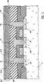
− 図4は、本発明により、強誘電材料の基板の残りの部分から薄膜を分離する段階を示した図;
− 図5は、本発明により得られた強誘電キャパシタメモリポイントの部分断面図である。
本発明による方法は下記の結晶質又は非結晶質固体材料に適用できる;
− 絶縁材料又は誘電材料
− 導電材料、
− 非組織半導体材料
− 主として周囲温度における抵抗が略107Ω.cmよりも大きい半絶縁材料
− 単結晶金属、及び、通常は超伝導体。
従って、本発明によれば、固体単結晶水晶を用いて単結晶水晶の薄膜を形成することが可能である。また、磁気材料、圧電材料、強誘電材料、焦電材料、及び、非線形光学特性又は光電効果、音響光学効果を有した材料、の薄膜を得ることも可能である。
以下に、集積回路上に強誘電キャパシタメモリを構成する場合の実施形態について説明する。
図1の断面図において示される電子回路は最新の超小型電子技術を用いて構成される。いわゆる「プラグ(plug)」技術、機械・化学的酸化物プレーナー技術(mechanical-chemical oxide planarization technique)、及びいわゆる「ダマスク(damask)」技術が実行され、酸化物内と面一状態に酸化物内に埋め込まれた接続点(connectons)が形成されることとなる。
前記回路はP型シリコンの基板1の面2に構成される。この面2には複数のベッセル(vessel)が形成される。図1では、N+タイプのベッセル31,32,33のみを示しており、絶縁領域41及び42を得るべく、図の左側のベッセル31から右側のベッセル33にわたってフィールド酸化物が増加している。ベッセル31,32はMOS型の二つのトランジスタのドレンを構成するものであり、ベッセル32はそれらの共通のソースを構成するものである。前記面2には、酸化物の薄膜61,62を挟んで、多結晶シリコンワード線51,52の列が蒸着されている。ワード51,52の列は絶縁材料65,66の層によって被覆されている。この絶縁材料はまた、層63,64として領域41,42も被覆している。アルミニウムビット線8の列によって、前記ソース32との電気的接触が保証されている。上述した全ての要素をカバーするように酸化物層7が蒸着されている。酸化物層7には、TiNバリアー副層(TiN barrier sub-layer)の設けられた面一プラチナ電極(flush platinum electrodes)91,92が蒸着されている。電極91,92は「プラグ」11,12によってトランジスタドレン31,32に接続されている。上記各要素は埋め込まれており、従って回路は平坦な外面15を有したものとなっている。
次に、本発明のによる強誘電体の薄膜の形成方法について説明する。この薄膜はキャパシタ誘電体を形成するものである。
図2は、強誘電体材料、例えばPbZrTiO3(PZT)、から成る基板100の側面図である。この基板100の平坦面101はイオン(例えば200KeVでかつ1017cm-2の供与量の水素イオン)により衝撃を付与される。このイオン衝撃は図2において複数の矢印にて示してある。注入されたイオンによって前記平坦面101と平行な面に隣接した層102に微小キャビティが形成される。この注入材料による層102は極めて薄く、数十nm、例えば50ないし100nmのものである。この層が基板100を二つの領域、すなわち、前記平坦面101側に位置して薄膜を形成する第一の領域103と、基板の残り部分を形成する第二の領域104とに分ける。第一の領域の厚さは約800nmである。前記層102は多数の微小キャビティの層から成るものである。
強誘電材料100から成る基板の前記平坦面101、及び該半導体基板1に構成された電子回路の平坦面15は、互いを単に接触させただけて互いが着くように、例えば化学的に処理される。図3は互いに関連した二つの基板100及び1を示している。半導体基板1の平坦面15が、強誘電材料から成る基板100の平坦面101に付着している。
このアッセンブリは次いで約500℃で熱処理される。これにより、図4に示す如く、強誘電体材料から成る基板100の前記二つの領域103と104とが、層102のところから分離する。これによって、強誘電体材料の薄膜が取り付けられて成る電子回路の設けられた半導体材料が得られる。
薄膜103の外表面105は精細に研磨される。
共通電極16を薄膜103の平坦面105に蒸着することにより二つのキャパシタを用いたメモリポイントが形成されて成る、図5に示す如きデバイスが得られる。
最終段階では、回路全体の保護すべきパッケージングを施すことも可能である。
かかる強誘電体薄膜は、MOSトランジスタを構成すべくシリコンに直接堆積された強誘電体材料の層を構成するのにも用いられる。その場合、分極状態によって該トランジスタのOFF状態又はON状態を決定する制御ゲートがこの強誘電体層と置き換えられる。
特に、本発明による方法を誘電体に応用すれば、ガラス支持体又はシリカ支持体に耐磨耗サファイア層(β−アルミナ)を形成することができる。このようなアルミナ薄膜は、支持体として機能する前記ガラス又はシリカ(例えば光学部品)を磨耗及び傷から保護することができる。水素イオンを約8×10¹⁶atoms/cm2及び110keVで注入することにより薄膜又はサファイア層を約1μmの厚さにすることが可能である。この小さい厚さは、支持体として機能するガラス又はシリカを、その後、例えばレンズとなすために整形(shaping)する場合にも適合するものである。
本発明に係る方法は金属材料にも適用可能である。その場合、耐蝕層及び拡散バリアーを形成することが可能である。多結晶層の替わりに単結晶金属層を形成することができることで、特に化学的侵食に対する拡散バリアーの効率の点で優れた優位性を発揮する。実際、多結晶金属材料における結晶粒接続における重要な拡散現象の存在がこれらの材料内の薄膜の効率を制限する。一例として、鋼製基板上に500nm厚の単結晶ニオブを蒸着して、腐食性媒体中での耐熱性を有したものを得ることを考える。この薄膜を得るために、約2×10¹⁷atoms/cm2、200keVでのH+イオン注入を行う。
別の例は、情報を記憶するのに、磁区(バブル)及び磁壁(Bloch walls)を用いたメモリの形成に関するものである。この目的のため、非磁性ガーネットから成る固体基板が用いられ、該基板上に、フェリ磁性ガーネットの層がエピタキシアル成長によって成長させられる。本発明に係る該方法によってフェリ磁性ガーネット材料の薄膜を、支持体として機能しかつ集積回路を有したシリコン基板上に加えることが可能となる。これらの集積回路は、フェリ磁性ガーネットから成る薄膜内の磁区又は磁壁を駆動させ、変位させ、及び検出するために局部磁場を発生するのに適した電子デバイス、論理デバイス、アナログデバイス、及び、集積化されたマイクロワインディング(microwindings)と組み合わされている。The present invention relates to a method for forming a thin film of a solid material made of, for example, a dielectric, a conductor, and a semi-insulator. The thin film may be crystalline or amorphous. Further, it may be made of an amorphous semiconductor or a polycrystalline semiconductor. The crystal plane of the polycrystalline semiconductor may be oriented in any direction. Further, this material may have a ferroelectric property, a piezoelectric property, a magnetic property, a photoelectric property, and the like.
The method according to the invention has particular application in realizing ferroelectric capacitor memories.
Various methods for producing a thin film made of a solid material are known. These methods depend on the material properties and the required film thickness. For example, a thin film made of a solid material can be deposited on the surface of a member by a projection method, a spraying method, an electroplating method, or the like. A thin film can also be obtained by processing a required material to be thinned by mechanical chemical or chemical abrasion. The obtained thin film is then bonded or fixed on a member to be a support.
In general, the thin film is fixed to the surface of the member in order to improve the outer surface characteristics of the member.
In the field of semiconductor technology, for example, it may be necessary to produce a semiconductor thin film in order to produce so-called “silicon-on-insulator”. Until now, various techniques for producing semiconductor thin films have been developed. One of the latest technologies is to inject a rare gas or hydrogen ions into a semiconductor material to form an embrittled region at a depth close to the average ion penetration depth. French patent publication FR-A-2 681 472 discloses a method for obtaining a thin film of a semiconductor material using this characteristic. According to this method, a plate of the desired semiconductor material with a flat surface is processed in the following steps.
-First implantation stage: In this stage the flat surface of the plate is bombarded by ions. This creates a “gaseous microblister” layer at a depth close to the ion penetration depth inside the plate body. This layer separates the plate into a lower region constituting the substrate mass and an upper region constituting the thin film. The ions are selected from rare gas ions or hydrogen gas ions.
-Second stage: In this stage, the flat surface of the plate is placed in close proximity to a support of at least a layer of rigid material. This close placement, for example with an adhesive or by pre-treating the surface, further possibly heat treatment and / or electrostatic treatment to promote atomic bonds between the support and the plate. Is done.
Third heat treatment stage: In this stage, the plate-support assembly is heated. The heating temperature at that time is higher than the temperature at which the implantation is performed and the thin film is sufficiently separated from the substrate mass. The temperature is about 400 ° C. or more in the case of silicon.
This implantation is adapted to form a gaseous micro-bulge layer that becomes the fracture region in the final stage of the heat treatment. Thus, the micro-bulge layer generated in the plate body forms two regions separated by this layer, that is, a thin film, in the plate at a depth approximating the average ion penetration depth. And a region for forming the remaining portion of the substrate. In the third stage, the heat treatment is performed at a temperature sufficient to generate a fracture region and the two regions separate, such as a crystalline rearrangement effect in the semiconductor material, eg It is performed by a microcavity growth effect and / or a microblister pressure effect.
Depending on the injection conditions, for example, after injection of a gas such as hydrogen, the cavities or bulges can be viewed with a transmission electron microscope in some cases. In the case of silicon, a minute bulge having a size of several nm to several hundred nm can be seen. As a result, these cavities can only be seen in the heat treatment stage. In particular, it can be seen when the implantation temperature is low, so in this stage nucleation takes place so that a breakdown occurs between the thin film and the rest of the substrate at the end of the heat treatment stage.
Until now, it was considered that the method disclosed in French Patent Publication FR-A-2 681 472 can be applied only to thin film formation using a substrate made of a semiconductor material. In this publication, the following explanation is given for various phenomena known empirically. First, a first ion implantation is performed by exposing a flat surface of a plate of semiconductor material to an ion beam. This flat surface is substantially parallel to the main crystal plane when the semiconductor material is completely monocrystalline, or to the main crystal plane when the material is polycrystalline. , Slightly tilted with the same index for all grains. As a result, a layer of “gaseous micro-swell” corresponding to the embrittled region is formed at a depth substantially equal to the average ion penetration depth in the plate body, and the inside of the plate body is formed by this layer. It is separated into two regions: a region to be a thin film and a region that forms the rest of the substrate. Here, the “gaseous bulge portion” refers to a cavity or a microcavity generated when hydrogen gas ions or rare gas ions are implanted into a material. These cavities can take a very flat shape with a small height, for example of the order of a few cavities, or a substantially spherical shape, or none of them. These cavities may or may not contain free gas phase and / or gas atoms resulting from implanted ions fixed to the atoms of the material forming the walls of the cavity. These cavities are usually referred to as “microblisters”, “platelets”, or “bubbles”. In the third step, the heat treatment is performed at a temperature sufficient to separate the two regions in consideration of the treatment time. The time-temperature pair of this heat treatment is determined by the amount of implanted ions.
FR-A-2 681 472 discloses a method for obtaining a thin film using a substrate made of a semiconductor material having a crystal structure. The development of the various steps of the method is described as being based on the contact of implanted ions with a crystalline mesh of semiconductor material.
However, the inventors of the present invention have discovered the surprising fact that this method can be applied to all types of solid materials, crystalline or amorphous. This method is also applicable to dielectric materials, conductive materials, semiconductor materials, and amorphous semiconductor materials, as well as polycrystalline semiconductors that do not have a main crystal plane whose crystal grains are substantially parallel to the flat surface of the plate. Can do it. In addition to amorphous semiconductors, this polycrystalline semiconductor will hereinafter be referred to as unorganized semiconductors. Also, this method does not greatly change the properties of the material to which this method is applied.
The inventors of the present invention have also surprisingly found that the implantation of hydrogen gas ions or noble gas ions forms a microcavity in the solid material as well as the crystalline semiconductor material, and the subsequent heat treatment. Have found that the mass of the two separates into two parts at the microcavities. In fact, the heat treatment coalesces the microcavities regardless of the type of solid material, and embrittles the structure at the layer portion of the microcavities. This embrittlement allows material separation under the effect of internal stress and / or internal pressure within the microcavity. This separation is self-generated or due to the application of external stress.
The term layer of microcavities refers to regions that contain microcavities that are close to or far from each other at different depths.
Accordingly, an object of the present invention is to have no dielectric material, conductive material, semi-insulating material, non -textured semiconductor material, that is, an amorphous semiconductor material, or a main crystal plane in which crystal grains are substantially parallel to the flat surface of the plate. Providing a method of forming a thin film of crystalline or amorphous solid material selected from polycrystalline semiconductor, the method comprising the following steps in processing a substrate made of the above solid material: It is characterized by:
Noble gas ions on one side of the substrate so that a layer of microcavities separating the substrate into two regions is produced at a depth close to the average ion penetration depth in the body of the substrate. And an ion implantation step that imparts bombardment with ions selected from hydrogen ions;
-A heat treatment step for heating said microcavity layer to a temperature sufficient to separate said two regions of said substrate, either naturally or by applying stress ;
And fixing the surface of the substrate to a support, optionally provided between the ion implantation step and the heating step .
This optional fixation step may be necessary if the membrane is not rigid enough to be self-supporting. Usually, a thin film will be necessary because it is placed on a support. In that case, the support must be able to withstand the final heat treatment step.
The surface of the substrate is fixed to the support by an adhesive or a process suitable for interatomic bonding.
In particular, the method according to the invention can be applied to obtain a thin film of ferroelectric material using a substrate made of a ferroelectric material and also to fix it to a support.
Preferably, the support is made of a semiconductor material and at least one electronic control circuit is constructed on one side of the support. A thin film made of a ferroelectric material is fixed on the support so as to function as a dielectric for a memory capacitor controlled by the electronic control circuit so as to constitute a memory point.
The electronic control circuit is preferably of the MOS transistor type.
The method according to the present invention can also be applied to the formation of a sapphire thin film, a corrosion-resistant metal thin film, or a magnetic material thin film on a support.
Hereinafter, the present invention will be more clearly understood and further effects and features of the present invention will become apparent from the following detailed description with reference to the accompanying drawings. However, the present invention is not limited to the following examples.
1 is a partial cross-sectional view of an integrated circuit configured on one side of a semiconductor substrate;
FIG. 2 shows an ion implantation step carried out on one side of a substrate made of a ferroelectric material according to the invention;
FIG. 3 shows a fixing stage according to the invention, consisting of affixing the surface of a semiconductor substrate on which an integrated circuit has been formed to the surface of a substrate of ferroelectric material that has been bombarded by ions;
-Figure 4 shows the step of separating the thin film from the rest of the substrate of ferroelectric material according to the invention;
FIG. 5 is a partial cross-sectional view of a ferroelectric capacitor memory point obtained according to the present invention.
The method according to the invention can be applied to the following crystalline or amorphous solid materials:
-Insulating material or dielectric material-Conductive material,
-Non-textured semiconductor material-Semi-insulating material with a resistance greater than approximately 10 7 Ω.cm, mainly at ambient temperature-Single crystal metal and usually superconductor.
Therefore, according to the present invention, it is possible to form a thin film of single crystal quartz using solid single crystal quartz. It is also possible to obtain a thin film of a magnetic material, a piezoelectric material, a ferroelectric material, a pyroelectric material, and a material having nonlinear optical characteristics or a photoelectric effect or an acoustooptic effect.
Hereinafter, an embodiment in which a ferroelectric capacitor memory is formed on an integrated circuit will be described.
The electronic circuit shown in the cross-sectional view of FIG. 1 is constructed using the latest microelectronic technology. So-called “plug” technology, mechanical-chemical oxide planarization technique, and so-called “damask” technology have been implemented, and the oxide is flush with the oxide. The connection points embedded in are formed.
The circuit is formed on the
Next, a method for forming a ferroelectric thin film according to the present invention will be described. This thin film forms the capacitor dielectric.
FIG. 2 is a side view of a
The
This assembly is then heat treated at about 500 ° C. As a result, as shown in FIG. 4, the two
The
By depositing the
In the final stage, the entire circuit can be packaged to be protected.
Such ferroelectric thin films are also used to construct a layer of ferroelectric material deposited directly on silicon to form a MOS transistor. In this case, a control gate that determines the OFF state or the ON state of the transistor according to the polarization state is replaced with the ferroelectric layer.
In particular, if the method according to the present invention is applied to a dielectric, a wear-resistant sapphire layer (β-alumina) can be formed on a glass support or silica support. Such an alumina thin film can protect the glass or silica (for example, an optical component) functioning as a support from abrasion and scratches. By implanting hydrogen ions at about 8 × 10 16 atoms / cm 2 and 110 keV, the thin film or sapphire layer can be about 1 μm thick. This small thickness is also compatible when the glass or silica functioning as a support is subsequently shaped, for example to form a lens.
The method according to the present invention is also applicable to metal materials. In that case, it is possible to form a corrosion resistant layer and a diffusion barrier. The ability to form a single crystal metal layer instead of a polycrystalline layer exhibits an excellent advantage especially in terms of the efficiency of the diffusion barrier against chemical erosion. In fact, the presence of significant diffusion phenomena in grain connections in polycrystalline metal materials limits the efficiency of thin films in these materials. As an example, suppose that a single crystal niobium having a thickness of 500 nm is vapor-deposited on a steel substrate to obtain one having heat resistance in a corrosive medium. In order to obtain this thin film, H + ion implantation is performed at about 2 × 10 17 atoms / cm 2 and 200 keV.
Another example relates to the formation of a memory that uses magnetic domains (bubbles) and magnetic walls (Bloch walls) to store information. For this purpose, a solid substrate made of non-magnetic garnet is used, on which a layer of ferrimagnetic garnet is grown by epitaxial growth. The method according to the invention makes it possible to apply a thin film of ferrimagnetic garnet material on a silicon substrate which functions as a support and has integrated circuits. These integrated circuits are electronic, logic, analog, and integrated devices that are suitable for generating local magnetic fields to drive, displace, and detect magnetic domains or domain walls in thin films of ferrimagnetic garnet. Combined with integrated microwindings.
Claims (5)
前記強誘電体材料から成る基板(100)を下記の段階を含んだ工程により処理することを特徴とする薄膜形成方法:
− 前記基板(100)の本体内の平均イオン侵入深さに近い深さの位置に該基板を二つの領域(103,104)に分離する複数の微小キャビティから成る層(102)が生じるように、前記基板(100)の一方の面(101)に、水素イオンによって衝撃を付与するイオン注入段階;
支持体上に前記基板の一方の面(101)を固定する段階であって、前記支持体(1)が半導体材料から成り、少なくとも一つの電子制御回路がこの支持体(1)の一方の面(15)に構成され、かつ該支持体(1)上には、強誘電体材料から成る薄膜(103)が、前記電子制御回路により制御されるメモリキャパシタのための誘電体として機能してメモリポイントを構成するように固定されるところの段階;
− 前記微小キャビティの層(102)を500度以上の温度まで加熱する熱処理段階。A method of forming a thin film of ferroelectric material ,
A method of forming a thin film, comprising: treating a substrate (100) made of the ferroelectric material by a process including the following steps:
A layer (102) consisting of a plurality of microcavities separating the substrate into two regions (103, 104) is produced at a depth close to the average ion penetration depth in the body of the substrate (100). An ion implantation step of applying an impact by hydrogen ions to one surface (101) of the substrate (100);
Fixing one surface (101) of the substrate on a support, wherein the support (1) is made of a semiconductor material and at least one electronic control circuit is provided on one surface of the support (1); (15) and on the support (1), a thin film (103) made of a ferroelectric material functions as a dielectric for a memory capacitor controlled by the electronic control circuit. The stage where the points are fixed to form;
A heat treatment step for heating said microcavity layer (102) to a temperature of 500 ° C. or more .
Applications Claiming Priority (3)
| Application Number | Priority Date | Filing Date | Title |
|---|---|---|---|
| FR9606085A FR2748850B1 (en) | 1996-05-15 | 1996-05-15 | PROCESS FOR MAKING A THIN FILM OF SOLID MATERIAL AND APPLICATIONS OF THIS PROCESS |
| FR96/06085 | 1996-05-15 | ||
| PCT/FR1997/000842 WO1997043461A1 (en) | 1996-05-15 | 1997-05-13 | Method for making a thin film of solid material, and uses thereof |
Related Child Applications (1)
| Application Number | Title | Priority Date | Filing Date |
|---|---|---|---|
| JP2008213117A Division JP2009010409A (en) | 1996-05-15 | 2008-08-21 | Method for forming thin film of solid material, and applications of method |
Publications (2)
| Publication Number | Publication Date |
|---|---|
| JP2000510284A JP2000510284A (en) | 2000-08-08 |
| JP4659929B2 true JP4659929B2 (en) | 2011-03-30 |
Family
ID=9492176
Family Applications (2)
| Application Number | Title | Priority Date | Filing Date |
|---|---|---|---|
| JP54059597A Expired - Lifetime JP4659929B2 (en) | 1996-05-15 | 1997-05-13 | Method for forming thin film of solid material and application of the method |
| JP2008213117A Pending JP2009010409A (en) | 1996-05-15 | 2008-08-21 | Method for forming thin film of solid material, and applications of method |
Family Applications After (1)
| Application Number | Title | Priority Date | Filing Date |
|---|---|---|---|
| JP2008213117A Pending JP2009010409A (en) | 1996-05-15 | 2008-08-21 | Method for forming thin film of solid material, and applications of method |
Country Status (7)
| Country | Link |
|---|---|
| US (1) | US6190998B1 (en) |
| EP (1) | EP0902843B1 (en) |
| JP (2) | JP4659929B2 (en) |
| KR (1) | KR20000011051A (en) |
| DE (1) | DE69701571T2 (en) |
| FR (1) | FR2748850B1 (en) |
| WO (1) | WO1997043461A1 (en) |
Families Citing this family (87)
| Publication number | Priority date | Publication date | Assignee | Title |
|---|---|---|---|---|
| FR2748850B1 (en) * | 1996-05-15 | 1998-07-24 | Commissariat Energie Atomique | PROCESS FOR MAKING A THIN FILM OF SOLID MATERIAL AND APPLICATIONS OF THIS PROCESS |
| US6013563A (en) | 1997-05-12 | 2000-01-11 | Silicon Genesis Corporation | Controlled cleaning process |
| US6033974A (en) * | 1997-05-12 | 2000-03-07 | Silicon Genesis Corporation | Method for controlled cleaving process |
| US6582999B2 (en) | 1997-05-12 | 2003-06-24 | Silicon Genesis Corporation | Controlled cleavage process using pressurized fluid |
| US20070122997A1 (en) * | 1998-02-19 | 2007-05-31 | Silicon Genesis Corporation | Controlled process and resulting device |
| FR2773261B1 (en) | 1997-12-30 | 2000-01-28 | Commissariat Energie Atomique | METHOD FOR THE TRANSFER OF A THIN FILM COMPRISING A STEP OF CREATING INCLUSIONS |
| US6291314B1 (en) * | 1998-06-23 | 2001-09-18 | Silicon Genesis Corporation | Controlled cleavage process and device for patterned films using a release layer |
| US6242770B1 (en) | 1998-08-31 | 2001-06-05 | Gary Bela Bronner | Diode connected to a magnetic tunnel junction and self aligned with a metallic conductor and method for forming the same |
| FR2784796B1 (en) | 1998-10-15 | 2001-11-23 | Commissariat Energie Atomique | PROCESS FOR PRODUCING A LAYER OF MATERIAL BURIED IN ANOTHER MATERIAL |
| AU6905000A (en) * | 1999-08-10 | 2001-03-05 | Silicon Genesis Corporation | A cleaving process to fabricate multilayered substrates using low implantation doses |
| US6263941B1 (en) | 1999-08-10 | 2001-07-24 | Silicon Genesis Corporation | Nozzle for cleaving substrates |
| US6500732B1 (en) | 1999-08-10 | 2002-12-31 | Silicon Genesis Corporation | Cleaving process to fabricate multilayered substrates using low implantation doses |
| US6333202B1 (en) * | 1999-08-26 | 2001-12-25 | International Business Machines Corporation | Flip FERAM cell and method to form same |
| US6391658B1 (en) * | 1999-10-26 | 2002-05-21 | International Business Machines Corporation | Formation of arrays of microelectronic elements |
| US6544862B1 (en) * | 2000-01-14 | 2003-04-08 | Silicon Genesis Corporation | Particle distribution method and resulting structure for a layer transfer process |
| FR2809867B1 (en) * | 2000-05-30 | 2003-10-24 | Commissariat Energie Atomique | FRAGILE SUBSTRATE AND METHOD FOR MANUFACTURING SUCH SUBSTRATE |
| FR2811807B1 (en) * | 2000-07-12 | 2003-07-04 | Commissariat Energie Atomique | METHOD OF CUTTING A BLOCK OF MATERIAL AND FORMING A THIN FILM |
| WO2002015244A2 (en) * | 2000-08-16 | 2002-02-21 | Massachusetts Institute Of Technology | Process for producing semiconductor article using graded expitaxial growth |
| US8507361B2 (en) | 2000-11-27 | 2013-08-13 | Soitec | Fabrication of substrates with a useful layer of monocrystalline semiconductor material |
| FR2840731B3 (en) * | 2002-06-11 | 2004-07-30 | Soitec Silicon On Insulator | METHOD FOR MANUFACTURING A SUBSTRATE HAVING A USEFUL LAYER OF SINGLE-CRYSTAL SEMICONDUCTOR MATERIAL OF IMPROVED PROPERTIES |
| FR2894990B1 (en) * | 2005-12-21 | 2008-02-22 | Soitec Silicon On Insulator | PROCESS FOR PRODUCING SUBSTRATES, IN PARTICULAR FOR OPTICS, ELECTRONICS OR OPTOELECTRONICS AND SUBSTRATE OBTAINED BY SAID PROCESS |
| WO2002082514A1 (en) * | 2001-04-04 | 2002-10-17 | Massachusetts Institute Of Technology | A method for semiconductor device fabrication |
| FR2823596B1 (en) * | 2001-04-13 | 2004-08-20 | Commissariat Energie Atomique | SUBSTRATE OR DISMOUNTABLE STRUCTURE AND METHOD OF MAKING SAME |
| FR2823599B1 (en) | 2001-04-13 | 2004-12-17 | Commissariat Energie Atomique | DEMOMTABLE SUBSTRATE WITH CONTROLLED MECHANICAL HOLDING AND METHOD OF MAKING |
| US7045878B2 (en) * | 2001-05-18 | 2006-05-16 | Reveo, Inc. | Selectively bonded thin film layer and substrate layer for processing of useful devices |
| US6956268B2 (en) * | 2001-05-18 | 2005-10-18 | Reveo, Inc. | MEMS and method of manufacturing MEMS |
| US20090065471A1 (en) * | 2003-02-10 | 2009-03-12 | Faris Sadeg M | Micro-nozzle, nano-nozzle, manufacturing methods therefor, applications therefor |
| US6875671B2 (en) * | 2001-09-12 | 2005-04-05 | Reveo, Inc. | Method of fabricating vertical integrated circuits |
| US7163826B2 (en) * | 2001-09-12 | 2007-01-16 | Reveo, Inc | Method of fabricating multi layer devices on buried oxide layer substrates |
| US7033910B2 (en) * | 2001-09-12 | 2006-04-25 | Reveo, Inc. | Method of fabricating multi layer MEMS and microfluidic devices |
| FR2830983B1 (en) | 2001-10-11 | 2004-05-14 | Commissariat Energie Atomique | METHOD FOR MANUFACTURING THIN FILMS CONTAINING MICROCOMPONENTS |
| AU2003222003A1 (en) * | 2002-03-14 | 2003-09-29 | Amberwave Systems Corporation | Methods for fabricating strained layers on semiconductor substrates |
| KR100465630B1 (en) * | 2002-05-03 | 2005-01-13 | 주식회사 하이닉스반도체 | Method for fabricating wafer |
| US6995430B2 (en) * | 2002-06-07 | 2006-02-07 | Amberwave Systems Corporation | Strained-semiconductor-on-insulator device structures |
| US20030227057A1 (en) * | 2002-06-07 | 2003-12-11 | Lochtefeld Anthony J. | Strained-semiconductor-on-insulator device structures |
| US7307273B2 (en) * | 2002-06-07 | 2007-12-11 | Amberwave Systems Corporation | Control of strain in device layers by selective relaxation |
| US7335545B2 (en) * | 2002-06-07 | 2008-02-26 | Amberwave Systems Corporation | Control of strain in device layers by prevention of relaxation |
| US7074623B2 (en) * | 2002-06-07 | 2006-07-11 | Amberwave Systems Corporation | Methods of forming strained-semiconductor-on-insulator finFET device structures |
| FR2847075B1 (en) * | 2002-11-07 | 2005-02-18 | Commissariat Energie Atomique | PROCESS FOR FORMING A FRAGILE ZONE IN A SUBSTRATE BY CO-IMPLANTATION |
| US7176108B2 (en) | 2002-11-07 | 2007-02-13 | Soitec Silicon On Insulator | Method of detaching a thin film at moderate temperature after co-implantation |
| FR2848336B1 (en) | 2002-12-09 | 2005-10-28 | Commissariat Energie Atomique | METHOD FOR PRODUCING A STRESS STRUCTURE FOR DISSOCIATING |
| JP4794810B2 (en) * | 2003-03-20 | 2011-10-19 | シャープ株式会社 | Manufacturing method of semiconductor device |
| FR2856844B1 (en) | 2003-06-24 | 2006-02-17 | Commissariat Energie Atomique | HIGH PERFORMANCE CHIP INTEGRATED CIRCUIT |
| FR2857953B1 (en) | 2003-07-21 | 2006-01-13 | Commissariat Energie Atomique | STACKED STRUCTURE, AND METHOD FOR MANUFACTURING THE SAME |
| FR2861497B1 (en) | 2003-10-28 | 2006-02-10 | Soitec Silicon On Insulator | METHOD FOR CATASTROPHIC TRANSFER OF A FINE LAYER AFTER CO-IMPLANTATION |
| US7354815B2 (en) * | 2003-11-18 | 2008-04-08 | Silicon Genesis Corporation | Method for fabricating semiconductor devices using strained silicon bearing material |
| US7772087B2 (en) | 2003-12-19 | 2010-08-10 | Commissariat A L'energie Atomique | Method of catastrophic transfer of a thin film after co-implantation |
| US7393733B2 (en) * | 2004-12-01 | 2008-07-01 | Amberwave Systems Corporation | Methods of forming hybrid fin field-effect transistor structures |
| US20060113603A1 (en) * | 2004-12-01 | 2006-06-01 | Amberwave Systems Corporation | Hybrid semiconductor-on-insulator structures and related methods |
| US10374120B2 (en) * | 2005-02-18 | 2019-08-06 | Koninklijke Philips N.V. | High efficiency solar cells utilizing wafer bonding and layer transfer to integrate non-lattice matched materials |
| TW200707799A (en) * | 2005-04-21 | 2007-02-16 | Aonex Technologies Inc | Bonded intermediate substrate and method of making same |
| FR2886051B1 (en) | 2005-05-20 | 2007-08-10 | Commissariat Energie Atomique | METHOD FOR DETACHING THIN FILM |
| FR2889887B1 (en) | 2005-08-16 | 2007-11-09 | Commissariat Energie Atomique | METHOD FOR DEFERING A THIN LAYER ON A SUPPORT |
| FR2891281B1 (en) | 2005-09-28 | 2007-12-28 | Commissariat Energie Atomique | METHOD FOR MANUFACTURING A THIN FILM ELEMENT |
| FR2899378B1 (en) | 2006-03-29 | 2008-06-27 | Commissariat Energie Atomique | METHOD FOR DETACHING A THIN FILM BY FUSION OF PRECIPITS |
| US20070243703A1 (en) * | 2006-04-14 | 2007-10-18 | Aonex Technololgies, Inc. | Processes and structures for epitaxial growth on laminate substrates |
| US9362439B2 (en) | 2008-05-07 | 2016-06-07 | Silicon Genesis Corporation | Layer transfer of films utilizing controlled shear region |
| US8993410B2 (en) | 2006-09-08 | 2015-03-31 | Silicon Genesis Corporation | Substrate cleaving under controlled stress conditions |
| US8293619B2 (en) | 2008-08-28 | 2012-10-23 | Silicon Genesis Corporation | Layer transfer of films utilizing controlled propagation |
| US7811900B2 (en) * | 2006-09-08 | 2010-10-12 | Silicon Genesis Corporation | Method and structure for fabricating solar cells using a thick layer transfer process |
| US8124499B2 (en) * | 2006-11-06 | 2012-02-28 | Silicon Genesis Corporation | Method and structure for thick layer transfer using a linear accelerator |
| US20080128641A1 (en) * | 2006-11-08 | 2008-06-05 | Silicon Genesis Corporation | Apparatus and method for introducing particles using a radio frequency quadrupole linear accelerator for semiconductor materials |
| FR2910179B1 (en) | 2006-12-19 | 2009-03-13 | Commissariat Energie Atomique | METHOD FOR MANUFACTURING THIN LAYERS OF GaN BY IMPLANTATION AND RECYCLING OF A STARTING SUBSTRATE |
| US20080188011A1 (en) * | 2007-01-26 | 2008-08-07 | Silicon Genesis Corporation | Apparatus and method of temperature conrol during cleaving processes of thick film materials |
| WO2008123117A1 (en) * | 2007-03-26 | 2008-10-16 | Semiconductor Energy Laboratory Co., Ltd. | Soi substrate and method for manufacturing soi substrate |
| WO2008123116A1 (en) | 2007-03-26 | 2008-10-16 | Semiconductor Energy Laboratory Co., Ltd. | Soi substrate and method for manufacturing soi substrate |
| FR2914492A1 (en) * | 2007-03-27 | 2008-10-03 | Soitec Silicon On Insulator | Substrate's thin ferroelectric layer manufacturing method for manufacturing e.g. piezoelectric sensor, involves subjecting resulting structure having transferred thin layer to electrical field to improve ferroelectric properties of layer |
| SG178762A1 (en) * | 2007-04-13 | 2012-03-29 | Semiconductor Energy Lab | Display device, method for manufacturing display device, and soi substrate |
| US7732301B1 (en) | 2007-04-20 | 2010-06-08 | Pinnington Thomas Henry | Bonded intermediate substrate and method of making same |
| FR2919427B1 (en) * | 2007-07-26 | 2010-12-03 | Soitec Silicon On Insulator | STRUCTURE A RESERVOIR OF LOADS. |
| US20090278233A1 (en) * | 2007-07-26 | 2009-11-12 | Pinnington Thomas Henry | Bonded intermediate substrate and method of making same |
| FR2922359B1 (en) * | 2007-10-12 | 2009-12-18 | Commissariat Energie Atomique | METHOD FOR MANUFACTURING A MICROELECTRONIC STRUCTURE INVOLVING MOLECULAR COLLAGE |
| FR2924272B1 (en) * | 2007-11-28 | 2010-06-11 | Commissariat Energie Atomique | METHOD FOR TRANSFERRING FILMS |
| FR2925221B1 (en) | 2007-12-17 | 2010-02-19 | Commissariat Energie Atomique | METHOD FOR TRANSFERRING A THIN LAYER |
| FR2930674A1 (en) * | 2008-04-29 | 2009-10-30 | Soitec Silicon On Insulator | Heterostructure e.g. silicon-on-insulator type substrate, fabricating method for e.g. optoelectronic field, involves subjecting heterostructure to ionic implantation operation using ions of atomic species within ferroelectric thin layer |
| US8330126B2 (en) * | 2008-08-25 | 2012-12-11 | Silicon Genesis Corporation | Race track configuration and method for wafering silicon solar substrates |
| US7927975B2 (en) | 2009-02-04 | 2011-04-19 | Micron Technology, Inc. | Semiconductor material manufacture |
| US8329557B2 (en) * | 2009-05-13 | 2012-12-11 | Silicon Genesis Corporation | Techniques for forming thin films by implantation with reduced channeling |
| FR2947098A1 (en) | 2009-06-18 | 2010-12-24 | Commissariat Energie Atomique | METHOD OF TRANSFERRING A THIN LAYER TO A TARGET SUBSTRATE HAVING A THERMAL EXPANSION COEFFICIENT DIFFERENT FROM THAT OF THE THIN LAYER |
| FR2961719B1 (en) * | 2010-06-24 | 2013-09-27 | Soitec Silicon On Insulator | PROCESS FOR PROCESSING A PIECE OF A COMPOUND MATERIAL |
| JP5786393B2 (en) * | 2011-03-18 | 2015-09-30 | 株式会社村田製作所 | Quartz device manufacturing method |
| FR2978600B1 (en) | 2011-07-25 | 2014-02-07 | Soitec Silicon On Insulator | METHOD AND DEVICE FOR MANUFACTURING LAYER OF SEMICONDUCTOR MATERIAL |
| WO2014020387A1 (en) | 2012-07-31 | 2014-02-06 | Soitec | Methods of forming semiconductor structures including mems devices and integrated circuits on opposing sides of substrates, and related structures and devices |
| US9741918B2 (en) | 2013-10-07 | 2017-08-22 | Hypres, Inc. | Method for increasing the integration level of superconducting electronics circuits, and a resulting circuit |
| FR3064820B1 (en) | 2017-03-31 | 2019-11-29 | Soitec | METHOD FOR ADJUSTING THE STRAIN CONDITION OF A PIEZOELECTRIC FILM |
| FR3068508B1 (en) * | 2017-06-30 | 2019-07-26 | Soitec | METHOD OF TRANSFERRING A THIN LAYER TO A SUPPORT SUBSTRATE HAVING DIFFERENT THERMAL EXPANSION COEFFICIENTS |
| US10991617B2 (en) | 2018-05-15 | 2021-04-27 | Applied Materials, Inc. | Methods and apparatus for cleaving of semiconductor substrates |
Family Cites Families (10)
| Publication number | Priority date | Publication date | Assignee | Title |
|---|---|---|---|---|
| FR2506344B2 (en) | 1980-02-01 | 1986-07-11 | Commissariat Energie Atomique | SEMICONDUCTOR DOPING PROCESS |
| FR2475068B1 (en) | 1980-02-01 | 1986-05-16 | Commissariat Energie Atomique | SEMICONDUCTOR DOPING PROCESS |
| JPH02186614A (en) * | 1989-01-12 | 1990-07-20 | Seiko Epson Corp | Method of treating ferroelectric film |
| FR2681472B1 (en) * | 1991-09-18 | 1993-10-29 | Commissariat Energie Atomique | PROCESS FOR PRODUCING THIN FILMS OF SEMICONDUCTOR MATERIAL. |
| US5216572A (en) * | 1992-03-19 | 1993-06-01 | Ramtron International Corporation | Structure and method for increasing the dielectric constant of integrated ferroelectric capacitors |
| FR2714524B1 (en) | 1993-12-23 | 1996-01-26 | Commissariat Energie Atomique | PROCESS FOR MAKING A RELIEF STRUCTURE ON A SUPPORT IN SEMICONDUCTOR MATERIAL |
| FR2715501B1 (en) | 1994-01-26 | 1996-04-05 | Commissariat Energie Atomique | Method for depositing semiconductor wafers on a support. |
| FR2738671B1 (en) | 1995-09-13 | 1997-10-10 | Commissariat Energie Atomique | PROCESS FOR PRODUCING THIN FILMS WITH SEMICONDUCTOR MATERIAL |
| FR2748850B1 (en) * | 1996-05-15 | 1998-07-24 | Commissariat Energie Atomique | PROCESS FOR MAKING A THIN FILM OF SOLID MATERIAL AND APPLICATIONS OF THIS PROCESS |
| US6013563A (en) * | 1997-05-12 | 2000-01-11 | Silicon Genesis Corporation | Controlled cleaning process |
-
1996
- 1996-05-15 FR FR9606085A patent/FR2748850B1/en not_active Expired - Fee Related
-
1997
- 1997-05-13 KR KR1019980709202A patent/KR20000011051A/en not_active Application Discontinuation
- 1997-05-13 EP EP97924080A patent/EP0902843B1/en not_active Expired - Lifetime
- 1997-05-13 US US09/147,266 patent/US6190998B1/en not_active Expired - Lifetime
- 1997-05-13 DE DE69701571T patent/DE69701571T2/en not_active Expired - Lifetime
- 1997-05-13 WO PCT/FR1997/000842 patent/WO1997043461A1/en not_active Application Discontinuation
- 1997-05-13 JP JP54059597A patent/JP4659929B2/en not_active Expired - Lifetime
-
2008
- 2008-08-21 JP JP2008213117A patent/JP2009010409A/en active Pending
Also Published As
| Publication number | Publication date |
|---|---|
| DE69701571D1 (en) | 2000-05-04 |
| EP0902843B1 (en) | 2000-03-29 |
| EP0902843A1 (en) | 1999-03-24 |
| FR2748850A1 (en) | 1997-11-21 |
| JP2000510284A (en) | 2000-08-08 |
| US6190998B1 (en) | 2001-02-20 |
| DE69701571T2 (en) | 2000-10-19 |
| JP2009010409A (en) | 2009-01-15 |
| KR20000011051A (en) | 2000-02-25 |
| WO1997043461A1 (en) | 1997-11-20 |
| FR2748850B1 (en) | 1998-07-24 |
Similar Documents
| Publication | Publication Date | Title |
|---|---|---|
| JP4659929B2 (en) | Method for forming thin film of solid material and application of the method | |
| US6316333B1 (en) | Method for obtaining a thin film in particular semiconductor, comprising a protected ion zone and involving an ion implantation | |
| JP4222644B2 (en) | Manufacturing method of semiconductor material thin films, especially including electronic components | |
| JP3439968B2 (en) | Process for separating at least two constituent materials constituting one structure in contact with each other by ion implantation | |
| US7037806B1 (en) | Method of fabricating silicon-on-insulator semiconductor substrate using rare earth oxide or rare earth nitride | |
| JP4433321B2 (en) | Method for manufacturing one-transistor memory | |
| TW419827B (en) | Ferroelectric nonvolatile transistor and method of making same | |
| US5374578A (en) | Ozone gas processing for ferroelectric memory circuits | |
| US7528463B2 (en) | Semiconductor on insulator structure | |
| US6245645B1 (en) | Method of fabricating an SOI wafer | |
| KR20020032586A (en) | Thin film transistors and their manufacture | |
| JPS5873166A (en) | Capacitive pressure transducer and method of producing same | |
| US8067793B2 (en) | Semiconductor device including storage capacitor with yttrium oxide capacitor dielectric | |
| JPH07297377A (en) | Semiconductor device and manufacture thereof | |
| US6080593A (en) | Method of manufacturing ferroelectric memory | |
| JP3055782B2 (en) | How to manufacture thin film transistors | |
| JPH02208978A (en) | Semiconductor device | |
| KR100450788B1 (en) | Method for fabricating single crystalline silicon tft-fram to improve integration and embody high performance tft-fram | |
| WO2022176689A1 (en) | Composite wafer and method for producing same | |
| JPH05259386A (en) | Manufacture of ferroelectric thin film | |
| TW541623B (en) | Processing method to eliminate the internal stress of silicon layer | |
| JP2023179298A (en) | Semiconductor device and method of manufacturing the same | |
| JP2000068467A (en) | Manufacture of semiconductor memory device | |
| JPS6367333B2 (en) | ||
| JPH02290079A (en) | Manufacture of semiconductor device |
Legal Events
| Date | Code | Title | Description |
|---|---|---|---|
| A621 | Written request for application examination |
Free format text: JAPANESE INTERMEDIATE CODE: A621 Effective date: 20040405 |
|
| A131 | Notification of reasons for refusal |
Free format text: JAPANESE INTERMEDIATE CODE: A131 Effective date: 20070828 |
|
| A601 | Written request for extension of time |
Free format text: JAPANESE INTERMEDIATE CODE: A601 Effective date: 20071128 |
|
| A602 | Written permission of extension of time |
Free format text: JAPANESE INTERMEDIATE CODE: A602 Effective date: 20080121 |
|
| A521 | Request for written amendment filed |
Free format text: JAPANESE INTERMEDIATE CODE: A523 Effective date: 20080228 |
|
| A02 | Decision of refusal |
Free format text: JAPANESE INTERMEDIATE CODE: A02 Effective date: 20080422 |
|
| A521 | Request for written amendment filed |
Free format text: JAPANESE INTERMEDIATE CODE: A523 Effective date: 20080821 |
|
| A911 | Transfer to examiner for re-examination before appeal (zenchi) |
Free format text: JAPANESE INTERMEDIATE CODE: A911 Effective date: 20080911 |
|
| A912 | Re-examination (zenchi) completed and case transferred to appeal board |
Free format text: JAPANESE INTERMEDIATE CODE: A912 Effective date: 20080918 |
|
| A601 | Written request for extension of time |
Free format text: JAPANESE INTERMEDIATE CODE: A601 Effective date: 20100706 |
|
| A602 | Written permission of extension of time |
Free format text: JAPANESE INTERMEDIATE CODE: A602 Effective date: 20100709 |
|
| A01 | Written decision to grant a patent or to grant a registration (utility model) |
Free format text: JAPANESE INTERMEDIATE CODE: A01 |
|
| A61 | First payment of annual fees (during grant procedure) |
Free format text: JAPANESE INTERMEDIATE CODE: A61 Effective date: 20101228 |
|
| FPAY | Renewal fee payment (event date is renewal date of database) |
Free format text: PAYMENT UNTIL: 20140107 Year of fee payment: 3 |
|
| R150 | Certificate of patent or registration of utility model |
Free format text: JAPANESE INTERMEDIATE CODE: R150 |
|
| R250 | Receipt of annual fees |
Free format text: JAPANESE INTERMEDIATE CODE: R250 |
|
| R250 | Receipt of annual fees |
Free format text: JAPANESE INTERMEDIATE CODE: R250 |
|
| R250 | Receipt of annual fees |
Free format text: JAPANESE INTERMEDIATE CODE: R250 |
|
| R250 | Receipt of annual fees |
Free format text: JAPANESE INTERMEDIATE CODE: R250 |
|
| EXPY | Cancellation because of completion of term |