JP4659783B2 - Manufacturing method of back-illuminated image sensor - Google Patents
Manufacturing method of back-illuminated image sensor Download PDFInfo
- Publication number
- JP4659783B2 JP4659783B2 JP2007157460A JP2007157460A JP4659783B2 JP 4659783 B2 JP4659783 B2 JP 4659783B2 JP 2007157460 A JP2007157460 A JP 2007157460A JP 2007157460 A JP2007157460 A JP 2007157460A JP 4659783 B2 JP4659783 B2 JP 4659783B2
- Authority
- JP
- Japan
- Prior art keywords
- semiconductor substrate
- manufacturing
- forming step
- image sensor
- backside
- Prior art date
- Legal status (The legal status is an assumption and is not a legal conclusion. Google has not performed a legal analysis and makes no representation as to the accuracy of the status listed.)
- Expired - Fee Related
Links
- 238000004519 manufacturing process Methods 0.000 title claims description 54
- 239000000758 substrate Substances 0.000 claims description 141
- 239000004065 semiconductor Substances 0.000 claims description 70
- 238000003384 imaging method Methods 0.000 claims description 45
- 238000000034 method Methods 0.000 claims description 31
- 239000004020 conductor Substances 0.000 claims description 28
- 238000005286 illumination Methods 0.000 claims description 25
- 239000000463 material Substances 0.000 claims description 22
- 230000008569 process Effects 0.000 claims description 17
- 230000015572 biosynthetic process Effects 0.000 claims description 8
- 239000002313 adhesive film Substances 0.000 claims description 6
- 230000004044 response Effects 0.000 claims description 6
- 238000010438 heat treatment Methods 0.000 claims description 3
- XUIMIQQOPSSXEZ-UHFFFAOYSA-N Silicon Chemical compound [Si] XUIMIQQOPSSXEZ-UHFFFAOYSA-N 0.000 description 50
- 229910052710 silicon Inorganic materials 0.000 description 50
- 239000010703 silicon Substances 0.000 description 50
- 238000009825 accumulation Methods 0.000 description 9
- 229910021420 polycrystalline silicon Inorganic materials 0.000 description 8
- 229920005591 polysilicon Polymers 0.000 description 8
- XAGFODPZIPBFFR-UHFFFAOYSA-N aluminium Chemical compound [Al] XAGFODPZIPBFFR-UHFFFAOYSA-N 0.000 description 5
- 229910052782 aluminium Inorganic materials 0.000 description 5
- 238000005530 etching Methods 0.000 description 5
- 239000010410 layer Substances 0.000 description 5
- 229910004298 SiO 2 Inorganic materials 0.000 description 4
- 230000002093 peripheral effect Effects 0.000 description 3
- 239000012790 adhesive layer Substances 0.000 description 2
- 230000008901 benefit Effects 0.000 description 2
- 238000005229 chemical vapour deposition Methods 0.000 description 2
- 239000012535 impurity Substances 0.000 description 2
- 229910010272 inorganic material Inorganic materials 0.000 description 2
- 239000011147 inorganic material Substances 0.000 description 2
- 238000002955 isolation Methods 0.000 description 2
- 230000007246 mechanism Effects 0.000 description 2
- 238000000926 separation method Methods 0.000 description 2
- 238000005245 sintering Methods 0.000 description 2
- 238000012360 testing method Methods 0.000 description 2
- 239000012780 transparent material Substances 0.000 description 2
- RZVAJINKPMORJF-UHFFFAOYSA-N Acetaminophen Chemical compound CC(=O)NC1=CC=C(O)C=C1 RZVAJINKPMORJF-UHFFFAOYSA-N 0.000 description 1
- UFHFLCQGNIYNRP-UHFFFAOYSA-N Hydrogen Chemical compound [H][H] UFHFLCQGNIYNRP-UHFFFAOYSA-N 0.000 description 1
- 239000000853 adhesive Substances 0.000 description 1
- 230000001070 adhesive effect Effects 0.000 description 1
- 238000006243 chemical reaction Methods 0.000 description 1
- 238000001514 detection method Methods 0.000 description 1
- 238000010586 diagram Methods 0.000 description 1
- 238000005516 engineering process Methods 0.000 description 1
- 239000011521 glass Substances 0.000 description 1
- 229910052739 hydrogen Inorganic materials 0.000 description 1
- 239000001257 hydrogen Substances 0.000 description 1
- 238000003702 image correction Methods 0.000 description 1
- 239000000203 mixture Substances 0.000 description 1
- 230000035515 penetration Effects 0.000 description 1
- 238000000206 photolithography Methods 0.000 description 1
- 229920002120 photoresistant polymer Polymers 0.000 description 1
- 239000005297 pyrex Substances 0.000 description 1
- 230000005855 radiation Effects 0.000 description 1
- 230000009467 reduction Effects 0.000 description 1
Images


Classifications
-
- H—ELECTRICITY
- H01—ELECTRIC ELEMENTS
- H01L—SEMICONDUCTOR DEVICES NOT COVERED BY CLASS H10
- H01L27/00—Devices consisting of a plurality of semiconductor or other solid-state components formed in or on a common substrate
- H01L27/14—Devices consisting of a plurality of semiconductor or other solid-state components formed in or on a common substrate including semiconductor components sensitive to infrared radiation, light, electromagnetic radiation of shorter wavelength or corpuscular radiation and specially adapted either for the conversion of the energy of such radiation into electrical energy or for the control of electrical energy by such radiation
- H01L27/144—Devices controlled by radiation
- H01L27/146—Imager structures
- H01L27/14601—Structural or functional details thereof
- H01L27/14603—Special geometry or disposition of pixel-elements, address-lines or gate-electrodes
-
- H—ELECTRICITY
- H01—ELECTRIC ELEMENTS
- H01L—SEMICONDUCTOR DEVICES NOT COVERED BY CLASS H10
- H01L27/00—Devices consisting of a plurality of semiconductor or other solid-state components formed in or on a common substrate
- H01L27/14—Devices consisting of a plurality of semiconductor or other solid-state components formed in or on a common substrate including semiconductor components sensitive to infrared radiation, light, electromagnetic radiation of shorter wavelength or corpuscular radiation and specially adapted either for the conversion of the energy of such radiation into electrical energy or for the control of electrical energy by such radiation
- H01L27/144—Devices controlled by radiation
- H01L27/146—Imager structures
- H01L27/14601—Structural or functional details thereof
- H01L27/14636—Interconnect structures
-
- H—ELECTRICITY
- H01—ELECTRIC ELEMENTS
- H01L—SEMICONDUCTOR DEVICES NOT COVERED BY CLASS H10
- H01L27/00—Devices consisting of a plurality of semiconductor or other solid-state components formed in or on a common substrate
- H01L27/14—Devices consisting of a plurality of semiconductor or other solid-state components formed in or on a common substrate including semiconductor components sensitive to infrared radiation, light, electromagnetic radiation of shorter wavelength or corpuscular radiation and specially adapted either for the conversion of the energy of such radiation into electrical energy or for the control of electrical energy by such radiation
- H01L27/144—Devices controlled by radiation
- H01L27/146—Imager structures
- H01L27/14601—Structural or functional details thereof
- H01L27/1464—Back illuminated imager structures
Description
本発明は、半導体基板の裏面側から光を照射し、前記光に応じて前記半導体基板内で発生した電荷を、前記半導体基板の表面側から読み出して撮像を行う裏面照射型撮像素子の製造方法に関する。 The present invention relates to a method for manufacturing a backside illuminating type imaging device that irradiates light from the back side of a semiconductor substrate, reads out charges generated in the semiconductor substrate in response to the light from the front side of the semiconductor substrate, and performs imaging. About.
半導体基板の裏面側から光を照射し、この光に応じて半導体基板内で発生した電荷を、半導体基板の表面側に形成された電荷蓄積領域に蓄積し、ここに蓄積された電荷に応じた信号を、半導体基板の表面側に形成されたCCDやCMOS回路等によって外部に出力して撮像を行う裏面照射型撮像素子が提案されている。 Light is irradiated from the back side of the semiconductor substrate, and electric charges generated in the semiconductor substrate in response to the light are accumulated in a charge accumulation region formed on the front side of the semiconductor substrate, and according to the electric charges accumulated here There has been proposed a back-illuminated imaging device that outputs a signal to the outside by a CCD, a CMOS circuit or the like formed on the front surface side of a semiconductor substrate and performs imaging.
裏面照射型撮像素子における半導体基板(光電変換領域)の厚さは、可視光をほとんど吸収させるために10μm程度必要である。このため、裏面照射型撮像素子を製造する際には、まず、厚みのある半導体基板の表面に電荷蓄積領域やCCD等の構造物を形成した後、その構造物上に配線層を形成し、この上に接着層を介して支持基板を貼り付け、その後、半導体基板を例えば10μmの厚さとなるまで裏面側からエッチングし、エッチング後は、半導体基板の表面側に形成した構造物に合わせて、半導体基板の裏面上にカラーフィルタやマイクロレンズ等の構造物を形成するといった手順をとる必要がある。 The thickness of the semiconductor substrate (photoelectric conversion region) in the back-illuminated image sensor is about 10 μm in order to absorb almost all visible light. For this reason, when manufacturing a back-illuminated image sensor, first, a structure such as a charge storage region or CCD is formed on the surface of a thick semiconductor substrate, and then a wiring layer is formed on the structure. A support substrate is pasted thereon via an adhesive layer, and then the semiconductor substrate is etched from the back side to a thickness of, for example, 10 μm. After etching, in accordance with the structure formed on the front side of the semiconductor substrate, It is necessary to take a procedure such as forming a structure such as a color filter or a microlens on the back surface of the semiconductor substrate.
このように形成した裏面照射型撮像素子において、半導体基板表面側に形成した配線層と接続するパッドを、半導体基板の裏面側又は表面側に形成する必要がある。現在普及している一般的なイメージセンサでは、光の入射する側にパッド開口を設けた構造となっており、この構造に対応して、ウエハ状態で各チップの機能テストを行う設備が製造ラインに設置されている。このため、裏面照射型撮像素子においては、パッド開口を半導体基板の表面側に形成してしまうと、これらのテストを行う設備を大幅に改造する必要が発生し、製造コストを増加させることになってしまう。 In the back-illuminated image sensor formed in this way, it is necessary to form a pad connected to the wiring layer formed on the semiconductor substrate surface side on the back surface side or the surface side of the semiconductor substrate. In general image sensors that are currently in widespread use, a pad opening is provided on the light incident side, and equipment for testing the function of each chip in the wafer state is available on the production line. Is installed. For this reason, if the pad opening is formed on the front surface side of the semiconductor substrate in the backside illuminating type imaging device, it is necessary to significantly modify the equipment for performing these tests, which increases the manufacturing cost. End up.
そこで、一般的なイメージセンサと同様に、裏面照射型撮像素子においても、光の入射する側(裏面側)にパッド開口を設ける方法がいろいろと提案されている。その一つは、表面側に形成した配線層に接続されたパッドを、半導体基板に裏面側からスルーホールを形成して、裏面から露出させる方法である(例えば、特許文献1,2参照)。このような方法は、裏面側にカラーフィルタやマイクロレンズを形成する工程の前にスルーホールを形成する場合、カラーフィルタやマイクロレンズの材料がスルーホールに留まってしまって、その後の工程で除去できなくなったり、この材料を塗布する基板に大きな段差が形成されているために塗布物の膜厚ムラが発生して、画面上斜めに線を引いたような固定パターンノイズが発生したりといった問題点がある。カラーフィルタやマイクロレンズを形成した後にスルーホールを形成する場合でも、スルーホールを定義するフォトレジストの除去をカラーフィルタやマイクロレンズに害を与えずに実施する必要があり、この実施が難しい。特に、上述したように、半導体基板の厚みが10μmもあると、上記問題点がより顕著となると共に、上記実施もより難しくなる。
Thus, as with a general image sensor, various methods for providing a pad opening on the light incident side (back side) have been proposed for back side illumination type imaging devices. One of them is a method of exposing a pad connected to a wiring layer formed on the front surface side from the back surface by forming a through hole in the semiconductor substrate from the back surface side (see, for example,
そこで、特許文献3に開示されているように、半導体基板表面から裏面まで達するトレンチを半導体基板に形成し、このトレンチに導電性材料を埋め込み、埋め込んだ導電性材料上にパッドを形成する方法を採用することも考えられる。パッドに対応するトレンチに導電性材料を埋め込むことは原理的には可能と言える。しかし、通常、パッドは100μm×100μm程度の大きさがあり、これと同程度の大きさのトレンチを形成し、ここに導電性材料を埋め込もうとすると、CVD法で形成するのであれば、導電性材料を50μm以上の膜厚で成膜し、同じ膜厚を異方性エッチングで除去する必要がある。このような工程は、半導体製造工程としてはとても現実的とは言えない。
Therefore, as disclosed in
トレンチサイズを小さくすれば製造工程的に問題はないが、この場合はトレンチに埋め込んだ導電性材料の抵抗値が高くなってしまうといった素子特性に関わる問題が発生する。 If the trench size is reduced, there is no problem in the manufacturing process, but in this case, a problem relating to element characteristics such as an increase in the resistance value of the conductive material embedded in the trench occurs.
本発明は、上記事情に鑑みてなされたものであり、光入射側にパッド開口を設けながらも、製造コストの増大及びパッド配線間の抵抗の増加を防ぐことが可能な裏面照射型撮像素子の製造方法を提供することを目的とする。 The present invention has been made in view of the above circumstances, and is a back-illuminated imaging device capable of preventing an increase in manufacturing cost and an increase in resistance between pad wirings while providing a pad opening on the light incident side . An object is to provide a manufacturing method .
本発明の裏面照射型撮像素子は、半導体基板の裏面側から光を照射し、前記光に応じて前記半導体基板内で発生した電荷を、前記半導体基板の表面側から読み出して撮像を行う裏面照射型撮像素子であって、前記半導体基板の裏面上に形成されたパッド部と、前記半導体基板内に形成され、前記半導体基板の表面上に形成された配線部と前記パッド部とを電気的に接続するための複数のコンタクト配線部とを備える。 The backside illumination type imaging device of the present invention irradiates light from the backside of the semiconductor substrate, and reads back the charge generated in the semiconductor substrate in response to the light from the topside of the semiconductor substrate to perform imaging. An image pickup device, wherein a pad portion formed on the back surface of the semiconductor substrate, and a wiring portion formed in the semiconductor substrate and formed on the front surface of the semiconductor substrate are electrically connected to the pad portion. And a plurality of contact wiring portions for connection.
本発明の裏面照射型撮像素子は、前記半導体基板内に形成され、前記半導体基板の表面側の構成要素と裏面側の構成要素との位置合わせを行うための多数の合わせマークとを備え、前記多数の合わせマークの各々は、前記半導体基板表面に対して垂直な方向に延びる導電性材料の複数の柱のパターンによって構成されている。 The backside-illuminated imaging device of the present invention comprises a large number of alignment marks formed in the semiconductor substrate, for aligning the components on the front surface side and the components on the back surface side of the semiconductor substrate, Each of the plurality of alignment marks is configured by a pattern of a plurality of columns of conductive material extending in a direction perpendicular to the surface of the semiconductor substrate.
本発明の裏面照射型撮像素子は、前記合わせマークを構成する複数の柱が二次元状に配置されている。 In the backside illumination type imaging device of the present invention, a plurality of columns constituting the alignment mark are two-dimensionally arranged.
本発明の裏面照射型撮像素子は、前記合わせマークを構成する複数の柱のパターンが対称となっている。 In the backside illuminating type image pickup device of the present invention, the pattern of the plurality of columns constituting the alignment mark is symmetric.
本発明の裏面照射型撮像素子は、前記合せマークを構成する複数の柱の各々の幅の最大となる部分の長さが2μm以下である。 In the backside illumination type image pickup device of the present invention, the length of the maximum width of each of the plurality of pillars constituting the alignment mark is 2 μm or less.
本発明の裏面照射型撮像素子は、前記合わせマークを構成する複数の柱の各々が前記半導体基板内の表面から裏面まで達している。また、本発明の裏面照射型撮像素子は、前記複数のコンタクト配線部の各々が、前記半導体基板の裏面から表面まで達する前記半導体基板表面に対して垂直な方向に延びた導電性材料の柱で構成されており、前記柱の一端に前記パッド部が接続され、前記柱の他端に前記配線部が接続されている。また、本発明の裏面照射型撮像素子は、前記複数のコンタクト配線部を構成する前記複数の柱が平面視において二次元状に配置されている。また、本発明の裏面照射型撮像素子は、前記複数のコンタクト配線部を構成する前記複数の柱の各々の幅の最大となる部分の長さが2μm以下である。 In the backside illumination type imaging device of the present invention, each of the plurality of columns constituting the alignment mark reaches from the front surface to the back surface in the semiconductor substrate. The backside illuminated image sensor of the present invention is a column of conductive material in which each of the plurality of contact wiring portions extends in a direction perpendicular to the semiconductor substrate surface reaching from the back surface to the surface of the semiconductor substrate. The pad portion is connected to one end of the column, and the wiring portion is connected to the other end of the column. Further, in the backside illumination type image pickup device of the present invention, the plurality of columns constituting the plurality of contact wiring portions are two-dimensionally arranged in a plan view. In the back-illuminated image sensor of the present invention, the length of the maximum width of each of the plurality of pillars constituting the plurality of contact wiring portions is 2 μm or less.
本発明の裏面照射型撮像素子は、前記半導体基板の表面に無機接着層を介して貼り合わされた支持基板を備える。 The backside illumination type imaging device of the present invention includes a support substrate bonded to the surface of the semiconductor substrate via an inorganic adhesive layer.
本発明の裏面照射型撮像素子は、前記支持基板が前記半導体基板と同一材料である。 In the backside illumination type imaging device of the present invention, the support substrate is made of the same material as the semiconductor substrate.
本発明の裏面照射型撮像素子は、前記半導体基板の裏面上方に形成された前記パッド部と同一材料からなる膜であって、前記半導体基板内に形成された画素部の一部を遮光するための遮光膜と前記画素部同士の間の境界を遮光するための遮光膜のいずれか又は両方を備える。 The backside illumination type imaging device of the present invention is a film made of the same material as the pad portion formed above the back surface of the semiconductor substrate, and shields a part of the pixel portion formed in the semiconductor substrate. The light shielding film and the light shielding film for shielding the boundary between the pixel portions are provided.
本発明の裏面照射型撮像素子の製造方法は、半導体基板の裏面側から光を照射し、前記光に応じて前記半導体基板内で発生した電荷を、前記半導体基板の表面側から読み出して撮像を行う裏面照射型撮像素子の製造方法であって、前記半導体基板の裏面上に形成する多数のパッド部の各々を形成すべき平面領域において前記半導体基板の表面から裏面まで達する複数の第一の貫通孔を前記表面側から形成する貫通孔形成工程と、前記複数の第一の貫通孔に導電性材料を埋めて、導電性材料の第一の柱を形成する柱形成工程と、前記半導体基板の表面上に、前記複数の第一の柱と接続される配線部を形成する配線部形成工程と、前記配線部の形成後、前記半導体基板の裏面上の前記多数の平面領域の各々に当該各々の平面領域に形成された前記複数の第一の柱と接続されるパッド部を形成するパッド部形成工程とを備える。 The method for manufacturing a backside illuminating type imaging device according to the present invention irradiates light from the backside of a semiconductor substrate, reads out charges generated in the semiconductor substrate in response to the light from the frontside of the semiconductor substrate, and performs imaging. A method of manufacturing a backside illuminating type imaging device, wherein a plurality of first penetrations extending from the front surface to the back surface of the semiconductor substrate in a planar region in which each of a large number of pad portions formed on the back surface of the semiconductor substrate is to be formed A through hole forming step of forming a hole from the surface side, a column forming step of filling the plurality of first through holes with a conductive material to form a first column of the conductive material, and A wiring portion forming step for forming a wiring portion connected to the plurality of first pillars on the surface; and after forming the wiring portion , each of the plurality of planar regions on the back surface of the semiconductor substrate. wherein formed on the flat region of the And a pad portion forming step of forming a pad portion connected to the first pillar of the number.
本発明の裏面照射型撮像素子の製造方法は、前記貫通孔形成工程では、前記半導体基板の表面側の構成要素と裏面側の構成要素との位置合わせを行うための多数の合わせマークの各々を形成すべき平面領域において前記半導体基板の表面から裏面まで達する複数の第二の貫通孔も形成し、前記柱形成工程では、前記複数の第二の貫通孔にも前記導電性材料を埋めて、導電性材料の第二の柱も形成し、前記複数の第二の柱のパターンによって1つの前記合わせマークを形成する。 In the manufacturing method of the backside illumination type imaging device of the present invention, in the through-hole forming step, each of a large number of alignment marks for aligning the front surface side component and the back surface side component of the semiconductor substrate is provided. In the planar region to be formed, a plurality of second through holes reaching from the front surface to the back surface of the semiconductor substrate are also formed, and in the column forming step, the conductive material is buried in the plurality of second through holes, A second column of conductive material is also formed, and one alignment mark is formed by the pattern of the plurality of second columns.
本発明の裏面照射型撮像素子の製造方法は、前記貫通孔形成工程では、前記複数の第二の貫通孔を平面視において二次元状に配置して形成する。 In the manufacturing method of the backside illumination type imaging device of the present invention, in the through hole forming step, the plurality of second through holes are two-dimensionally arranged in a plan view.
本発明の裏面照射型撮像素子の製造方法は、前記貫通孔形成工程では、前記複数の第二の貫通孔のパターンが対称となるように形成する。 In the method of manufacturing the backside illumination type imaging device of the present invention, in the through hole forming step, the patterns of the plurality of second through holes are formed so as to be symmetric.
本発明の裏面照射型撮像素子の製造方法は、前記貫通孔形成工程では、前記複数の第二の貫通孔の各々の幅の最大となる部分の長さが2μm以下となるように前記第二の貫通孔を形成する。また、本発明の裏面照射型撮像素子の製造方法は、前記貫通孔形成工程では、前記複数の第一の貫通孔を平面視において二次元状に配置して形成する。また、本発明の裏面照射型撮像素子の製造方法は、前記貫通孔形成工程では、前記複数の第一の貫通孔の各々の幅の最大となる部分の長さが2μm以下となるように前記第一の貫通孔を形成する。 In the method for manufacturing a backside illuminating type image pickup device according to the present invention, in the through hole forming step, the length of the maximum portion of each of the plurality of second through holes is 2 μm or less. Through-holes are formed. In the method for manufacturing a backside illumination type image pickup device of the present invention, in the through hole forming step, the plurality of first through holes are two-dimensionally arranged in a plan view. Further, in the method of manufacturing the backside illumination type imaging device of the present invention, in the through hole forming step, the length of the maximum width of each of the plurality of first through holes is 2 μm or less. A first through hole is formed.
本発明の裏面照射型撮像素子の製造方法は、前記半導体基板内に前記電荷を蓄積する電荷蓄積領域を含む画素部を形成する画素部形成工程を備え、前記パッド部形成工程は、遮光機能を有する導電性材料を前記裏面上に成膜する工程と、前記パッド部を形成する平面領域上方、一部の前記画素部上方、及び前記画素部間の境界上方のうち、前記平面領域と、前記一部の画素部と前記境界のいずれか又は両方の上方以外の前記導電性材料を除去する工程とを含む。 The manufacturing method of the backside illuminating type imaging device of the present invention includes a pixel portion forming step of forming a pixel portion including a charge accumulation region for accumulating the charge in the semiconductor substrate, and the pad portion forming step has a light shielding function. A step of forming a conductive material on the back surface; a plane area above the plane area where the pad part is formed; a part of the pixel part; and a boundary between the pixel parts; Removing a part of the pixel portion and the conductive material other than above one or both of the boundaries.
本発明の裏面照射型撮像素子の製造方法は、前記パッド部形成工程後に前記画素部に対応するカラーフィルタを前記画素部上方に形成するカラーフィルタ形成工程と、前記パッド部形成工程の後、前記カラーフィルタ形成工程の前に前記半導体基板を加熱する工程とを備える。 The backside illumination type imaging device manufacturing method of the present invention includes: a color filter forming step of forming a color filter corresponding to the pixel portion above the pixel portion after the pad portion forming step; and the pad portion forming step, Heating the semiconductor substrate before the color filter forming step.
本発明の裏面照射型撮像素子の製造方法は、前記半導体基板が、第一の半導体基板と第二の半導体基板とこれらに挟まれる酸化膜とからなるSOI基板の前記第一の半導体基板であり、前記配線部形成工程後、前記第一の半導体基板の表面側に無機接着膜を介して支持基板を貼り合わせる工程を備える。 In the method for manufacturing a backside illuminating type imaging device according to the present invention, the semiconductor substrate is the first semiconductor substrate of an SOI substrate including a first semiconductor substrate, a second semiconductor substrate, and an oxide film sandwiched therebetween. Then, after the wiring part forming step, a step of attaching a support substrate to the surface side of the first semiconductor substrate via an inorganic adhesive film is provided.
本発明の裏面照射型撮像素子の製造方法は、前記支持基板が前記第一の半導体基板と同一材料である。 In the manufacturing method of the backside illumination type imaging device of the present invention, the support substrate is the same material as the first semiconductor substrate.
本発明によれば、光入射側にパッド開口を設けながらも、製造コストの増大及びパッド配線間の抵抗の増加を防ぐことが可能な裏面照射型撮像素子を提供することができる。 According to the present invention, it is possible to provide a backside illuminating type imaging device capable of preventing an increase in manufacturing cost and an increase in resistance between pad wirings while providing a pad opening on the light incident side.
以下、本発明の実施形態について図面を参照して説明する。 Embodiments of the present invention will be described below with reference to the drawings.
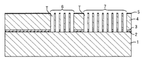
図1は、本発明の実施形態である裏面照射型撮像素子を光入射側(裏面)から見た平面模式図である。図2は、図1に示すA−A線断面模式図である。
図1に示すように、裏面照射型撮像素子100は、光を受光して撮像を行うための撮像領域30と、撮像領域30に形成されている裏面と反対の表面側の構成要素(電荷を蓄積するための電荷蓄積領域、電荷蓄積領域に蓄積された電荷に応じた信号を出力するための信号出力部等)と裏面側の構成要素(カラーフィルタ及びマイクロレンズ等)との位置合わせを行うための多数の合わせマークMが形成されるマーク形成領域と、表面側に形成されている配線部と接続されて外部との信号入出力を行うための多数のパッド部17が形成されるパッド形成領域とを有している。
FIG. 1 is a schematic plan view of a back-illuminated image sensor according to an embodiment of the present invention as viewed from the light incident side (back surface). 2 is a schematic cross-sectional view taken along line AA shown in FIG.
As shown in FIG. 1, the back-illuminated
合わせマークMは、図1の拡大図で示すように、上下左右に二次元状に配置された導電性材料(例えばドープトポリシリコン)の9つの柱8のパターンによって構成されている。図示したように、9つの柱8は、それぞれが例えば円柱であり、上下左右対称に配置されている。このような対称性を有していることで、9つの柱8から1つの合わせマークMの検出が可能となっている。柱8は、図2に示すように、半導体基板であるn型のシリコン基板4内にその裏面から表面まで達して形成されている。
As shown in the enlarged view of FIG. 1, the alignment mark M is configured by a pattern of nine
パッド部17は、図1の拡大図及び図2で示すように、その下方のシリコン基板4内にその裏面から表面まで達して形成された導電性材料(例えばドープトポリシリコン)の複数の柱9と接続されており、この複数の柱9の各々が、シリコン基板4の表面側に形成された配線部12に接続されている。図1の拡大図で示したように、柱9は、例えば円柱となっており、上下左右対称に二次元状に配置されている。柱9は、パッド部17と配線部12とを電気的に接続できれば良いため、対称に配置されている必要はない。又、二次元状に配置されていなくとも良い。
As shown in the enlarged view of FIG. 1 and FIG. 2, the
図2に示すように、裏面照射型撮像素子100は、シリコン基板4の裏面側から光を入射して用いるものである。マイクロレンズ21で集光され、カラーフィルタ20で分光された光はシリコン基板4に入射する。そして、ここで発生した電荷は電荷蓄積領域10に蓄積され、蓄積された電荷に応じた信号がMOSトランジスタからなるMOS回路によって外部に出力される。本明細書では、シリコン基板4の表面及び裏面を規準として、各構成要素の位置関係を定義するものとする。例えば、シリコン基板4の表面を規準としたときは、光の入射方向を該表面の上方向と定義し、シリコン基板4の裏面を規準としたときは、光の入射方向とは反対方向を該裏面の上方向と定義する。
As shown in FIG. 2, the backside illumination
裏面照射型撮像素子100は、シリコン基板4と、シリコン基板4の表面上に形成されたSiO2等の絶縁膜5と、絶縁膜5上に形成された絶縁膜14と、絶縁膜14上に接着膜15を介して形成された支持基板16とを備える。
Backside illuminated
接着膜15は、CVD法によって形成されたSiO2等の無機材料膜で構成されている。支持基板16は、熱膨張係数がシリコン基板4と近い材料を用いることが好ましい。これは、後述するシンター処理によるシリコン基板4へのダメージを減らすためである。しかし、このような材料であっても、例えばパイレックス等を用いると、その材料中に含まれる放射性同位元素から放出される放射線(特にα線)によって白キズが発生してしまう。この白キズは、裏面照射型撮像素子100がカメラに組み込まれた後にも発生するものであり、後発白キズと呼ばれる。この後発白キズは、画像補正処理を行う対象とならないキズとなってしまうため、深刻な問題となる。このため、支持基板16は、熱膨張係数がシリコン基板4と近い材料で且つ放射性同位元素をあまり含まない材料を用いることがより好ましい。
The
更に、支持基板16は透明性の高い材料であることが望ましい。支持基板16が透明であれば、上下に合わせ機構を持つ露光装置によって裏面照射型撮像素子100の表面側から合わせマークMを検出し、これを基準にして裏面側の構成要素を形成することが可能となるためである。この場合、合わせマークMは、シリコン基板4内に形成しておく必要はなく、シリコン基板4の表面上に形成しておけば充分である。
Furthermore, the
透明性の高い材料としては、ガラス基板があげられるが、これはシリコンと熱膨張係数が違ったり放射性同位元素が多かったりするため使いにくい。従って、支持基板として、熱膨張係数がシリコン基板4と近く、且つ、放射性同位元素をあまり含まないシリコンを使うことが好ましい。ただしシリコンは不透明なので上下に合わせ機構を持つ露光装置を使うことができない。そこで、本発明のように裏面側から見える合わせマークを形成しておくことが有効となる。
A highly transparent material is a glass substrate, which is difficult to use because it has a different thermal expansion coefficient than that of silicon and has many radioisotopes. Therefore, it is preferable to use silicon that has a thermal expansion coefficient close to that of the
撮像領域30にあるシリコン基板4内には、入射光に応じてシリコン基板4内で発生した電荷を蓄積するための電荷蓄積領域10と、ここに蓄積された電荷に応じた信号を読み出すためのMOSトランジスタからなるMOS回路の構成要素(不図示)等を含む画素部が二次元状に多数形成されている。又、シリコン基板4の表面から内側には、画素部同士を分離するための画素分離領域11が形成されている。
In the
シリコン基板4の裏面から内側には、暗電流を防ぐための高濃度のp型不純物領域3が形成されている。シリコン基板4のパッド形成領域には、多数のパッド部17の各々の下に、シリコン基板4の裏面から表面まで達する柱9が複数(図では9つだけ図示し、他は省略している)形成されており、パッド部17と複数の柱9の各々との電気的接続が行われている。シリコン基板4のマーク形成領域には、多数の合わせマークMの各々を形成すべき位置に、シリコン基板4の裏面から表面まで達する複数の柱8(図では5つだけ図示し、他は省略している)が形成されている。柱8及び柱9は、平面視においてそれぞれ同じサイズであり、そのサイズは、幅の最大となる部分の長さが2μm以下(円柱の場合は直径が2μm以下)となっていることが製造の容易さから望ましい。柱8及び柱9は、それぞれ、絶縁膜によってその側壁が覆われている。
A high-concentration p-
尚、柱8及び柱9は、それぞれ異なるサイズであっても良い。又、パッド部17に接続される複数の柱9の各々のサイズも同一でなく、ばらばらであっても良い。但し、いずれの場合も、柱8,9のサイズは2μm以下とすることが望ましい。又、柱8は、シリコン基板4の表面側と裏面側の双方から検出することができれば良いため、シリコン基板4の裏面から表面まで達している必要はなく、シリコン基板4内に埋設されていれば充分である。同様の理由から、柱8は柱9のように導電性材料で構成しておく必要もない。柱8と柱9を、それぞれシリコン基板4の裏面から表面まで達する柱状の導電性材料とすることにより、これらを同時に形成することができ、製造工程上有利となる。
Note that the
裏面照射型撮像素子100は、更に、シリコン基板4の裏面上のパッド部17を除く面上に形成された酸化膜2と、黒レベル検出用の画素部上方の酸化膜2上に形成された遮光膜18と、黒レベル検出用の画素部を除く画素部同士を分離する画素分離領域11上方の酸化膜2上に形成された画素間の混色を防ぐための遮光膜19と、画素部上方の酸化膜2上に形成されたカラーフィルタ20と、カラーフィルタ20上に形成されたマイクロレンズ21と、カラーフィルタ20及びマイクロレンズ21形成時の成膜材料からなる材料膜22とを備える。材料膜22には、パッド部17上に開口が形成され、ここからパッド部17が露出している。
The back-illuminated
パッド部17と遮光膜18と遮光膜19は、それぞれ同一材料であることが好ましい。これらが同一材料であれば、これらを同一工程で形成することができ、製造工程上有利なためである。遮光機能を実現しつつ、パッド部として機能させることができる材料としては、例えばアルミニウムが挙げられる。
The
絶縁膜14内には、シリコン基板4内の電荷蓄積領域10に蓄積された電荷に応じた信号を出力するMOS回路の構成要素及び周辺回路に接続される各種配線等の配線部12が形成されている。図示の例では、配線部12は3層配線構造となっている。配線部12は、MOS回路の構成要素及び周辺回路に接続される各種配線と柱9とを接続するためのコンタクト配線13を含んでおり、これにより、配線部12とパッド部17とが柱9を介して電気的に接続されている。
In the insulating
次に、以上のような構成の裏面照射型撮像素子100の製造方法を説明する。
図3〜図8は、裏面照射型撮像素子100の製造時の各工程における断面模式図である。
まず、図3に示すように、裏面から内側にp型不純物層3をドープしたn型のシリコン基板4と、n型のシリコン基板1と、シリコン基板4の裏面とシリコン基板1との間に形成された酸化膜2とからなるSOI基板を用意する。
Next, a manufacturing method of the backside illumination
3 to 8 are schematic cross-sectional views in respective steps during manufacturing of the backside illumination
First, as shown in FIG. 3, an n-
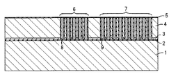
次に、シリコン基板4の表面上に例えばSiO2を成膜して絶縁膜5を形成し、絶縁膜5上の柱8を形成すべき位置と、柱9を形成すべき位置とに開口を形成したレジストマスクパターンを例えばフォトリソグラフィ法によって形成する。次に、このマスクパターンを介してマスク開口下方の絶縁膜5、シリコン基板4、及び酸化膜2をエッチングして除去し、マーク形成領域6とパッド形成領域7とにそれぞれ円柱状の貫通孔Tを形成する(図4)。貫通孔Tの直径は例えば0.8μmとなるようにマスクパターンを設計しておく。
Next, for example, SiO 2 is formed on the surface of the
次に、貫通孔Tの側壁を酸化して側壁に絶縁膜を形成し、絶縁膜5上に導電性材料としてドープトポリシリコンを成膜する。次に成膜したドープトポリシリコンをエッチバックして貫通孔Tにドープトポリシリコンを埋め込み、埋め込んだドープトポリシリコンの露出面を酸化させて柱8及び柱9を形成する(図5)。
Next, the side wall of the through hole T is oxidized to form an insulating film on the side wall, and doped polysilicon is formed as a conductive material on the insulating
次に、柱8によって構成される合わせマークMをシリコン基板4の表面側から検出し、これを基準にしてシリコン基板4の表面から内側に電荷蓄積領域10及び画素分離領域11を含む画素部を公知のプロセスによって形成する。次に、絶縁膜5上にMOS回路の構成要素や周辺回路や配線部12を形成し、この上に絶縁膜14を形成して平坦化する(図6)。配線部12のコンタクト配線13は、柱9上の絶縁膜5に開口を形成し、この開口内にポリシリコンを埋め込むことで形成する。
Next, the alignment mark M constituted by the
次に、CVD法によって表面にSiO2からなる接着膜15を形成した支持基板16(材料をシリコンとする)を用意し、この支持基板16を、接着膜15を介して絶縁膜14に直接接合技術によって貼り合わせる(図7)。次に、支持基板16を土台としてシリコン基板1をエッチング除去し、酸化膜2を露出させる(図8)。
Next, a support substrate 16 (material is silicon) having an
次に、パッド形成領域7上の酸化膜2をエッチングによって除去して柱9を露出させた後、酸化膜2上に導電性材料として例えばアルミニウムを成膜する。次に、アルミニウム膜上に、パッド形成領域7、黒レベル検出用の画素部上方、及び画素部間の画素分離領域11上方以外に開口を設けたレジストマスクパターンを形成する。次に、このマスクパターンを介してアルミニウム膜をエッチングして、パッド部17と遮光膜18,19を形成する。
Next, after the
次に、柱9を構成するドープトポリシリコンとパッド部17を構成するアルミニウムとの電気的接続を確実にするために、400℃前後の水素含有雰囲気での加熱処理(シンター)を行う。次に、カラーフィルタ20を形成し、マイクロレンズ21を形成して、最後に、カラーフィルタ20及びマイクロレンズ21形成時に形成された材料膜22のパッド部17上方に開口を形成してパッド部17を露出させて、図1に示す裏面照射型撮像素子100を完成する。
Next, in order to ensure electrical connection between the doped polysilicon constituting the
以上のように、裏面照射型撮像素子100によれば、シリコン基板4の裏面側に形成されたパッド部17と、表面側の配線部12とを複数の柱9によって電気的に接続する構成としたため、柱9のサイズを大きくしなくとも、パッド部17及び配線部12間の抵抗値を低く抑えながら、電気的接続を行うことが可能となる。柱9のサイズを小さく(2μm以下に)することができるため、上述した製造方法を採用した場合に、貫通孔Tに導電性材料を埋め込む工程の負荷を少なくすることができ、低コスト化を実現することができる。
As described above, according to the backside illuminating type
又、裏面照射型撮像素子100によれば、サイズの小さい複数の柱8のパターンによって合わせマークMを構成しているため、合わせマークMを形成する際の工程負荷を少なくすることができ、低コスト化を実現することができる。又、柱9と柱8を同じ長さ同じ材料としているため、上述した製造方法のように柱8と柱9を同時に形成することが可能となり、製造コストを削減することができる。
Further, according to the backside illumination type
又、裏面照射型撮像素子100によれば、シリコン基板4と支持基板16とが無機材料によって貼り合わせられているため、パッド部17と柱9との電気的接続を確実にするためのシンター処理によって、シリコン基板4と支持基板16との接着力が弱くなったり、支持基板16に反りが発生したりといったことがない。つまり、支持基板16とシリコン基板4とを完全に平行にした状態でカラーフィルタ20やマイクロレンズ21を形成することが可能である。したがって、カラーフィルタ20やマイクロレンズ21が設計通りのものとなり、歩留まりの低下によるコスト削減を実現することができる。
Further, according to the backside illumination
又、裏面照射型撮像素子100によれば、パッド部17に接続される複数の柱9が、二次元状に配置されているため、電気抵抗が小さくなり、パッド電極へのボンディング性が向上するといった利点がある。
In addition, according to the backside illuminating type
又、裏面照射型撮像素子100によれば、支持基板16とシリコン基板4とが同一材料で構成されているため、後発白キズの発生を防止することができる、シンター処理時のシリコン基板4へのダメージを減らすことができるといった利点がある。
Further, according to the backside illuminating type
又、裏面照射型撮像素子100によれば、パッド部17と遮光膜18,19とが同一材料で構成されているため、上述した製造方法のように、これらを同時に形成することが可能となり、製造コストを削減することができる。
Further, according to the backside illumination
尚、以上の説明では裏面照射型撮像素子100をMOS型としたが、CCD型であっても良い。又、裏面側の構成要素の合わせズレを検査するためのマークをシリコン基板4内に形成し、このマークを複数の柱で構成することも有効である。
In the above description, the back-illuminated
4 シリコン基板
9 導電性材料の柱
12 配線部
17 パッド部
100 裏面照射型撮像素子
4
Claims (10)
前記半導体基板の裏面上に形成する多数のパッド部の各々を形成すべき平面領域において前記半導体基板の表面から裏面まで達する複数の第一の貫通孔を前記表面側から形成する貫通孔形成工程と、 A through hole forming step of forming a plurality of first through holes from the front surface side to the back surface of the semiconductor substrate in a planar region in which each of a large number of pad portions to be formed on the back surface of the semiconductor substrate is to be formed; ,
前記複数の第一の貫通孔に導電性材料を埋めて、導電性材料の第一の柱を形成する柱形成工程と、 A column forming step of burying a conductive material in the plurality of first through holes to form a first column of the conductive material;
前記半導体基板の表面上に、前記複数の第一の柱と接続される配線部を形成する配線部形成工程と、 A wiring part forming step for forming a wiring part connected to the plurality of first pillars on the surface of the semiconductor substrate;
前記配線部の形成後、前記半導体基板の裏面上の前記多数の平面領域の各々に当該各々の平面領域に形成された前記複数の第一の柱と接続されるパッド部を形成するパッド部形成工程とを備え、 After the wiring portion is formed, pad portion formation for forming pad portions connected to the plurality of first pillars formed in the respective planar regions in each of the plurality of planar regions on the back surface of the semiconductor substrate A process,
前記貫通孔形成工程では、前記半導体基板の表面側の構成要素と裏面側の構成要素との位置合わせを行うための多数の合わせマークの各々を形成すべき平面領域において前記半導体基板の表面から裏面まで達する複数の第二の貫通孔も形成し、 In the through-hole forming step, from the front surface to the back surface of the semiconductor substrate in a planar region in which each of a large number of alignment marks for performing alignment between the front surface side component and the back surface side component of the semiconductor substrate is to be formed. A plurality of second through holes reaching up to
前記柱形成工程では、前記複数の第二の貫通孔にも前記導電性材料を埋めて、導電性材料の第二の柱も形成し、 In the column forming step, the conductive material is buried in the plurality of second through holes to form a second column of conductive material,
前記複数の第二の柱のパターンによって1つの前記合わせマークを形成する裏面照射型撮像素子の製造方法。 The manufacturing method of the backside-illumination type image pick-up element which forms one said alignment mark with the pattern of these 2nd pillars.
前記貫通孔形成工程では、前記複数の第二の貫通孔を平面視において二次元状に配置して形成する裏面照射型撮像素子の製造方法。 In the through-hole forming step, a method of manufacturing a backside-illuminated imaging device, wherein the plurality of second through-holes are arranged and formed two-dimensionally in a plan view.
前記貫通孔形成工程では、前記複数の第二の貫通孔のパターンが対称となるように形成する裏面照射型撮像素子の製造方法。 In the through-hole forming step, the backside-illuminated image sensor manufacturing method is formed such that the patterns of the plurality of second through-holes are symmetrical.
前記貫通孔形成工程では、前記複数の第二の貫通孔の各々の幅の最大となる部分の長さが2μm以下となるように前記第二の貫通孔を形成する裏面照射型撮像素子の製造方法。 In the through-hole forming step, the backside-illuminated image sensor is formed in which the second through-hole is formed so that the length of the maximum width of each of the plurality of second through-holes is 2 μm or less. Method.
前記貫通孔形成工程では、前記複数の第一の貫通孔を平面視において二次元状に配置して形成する裏面照射型撮像素子の製造方法。 In the through-hole forming step, a method of manufacturing a backside-illuminated image sensor in which the plurality of first through-holes are two-dimensionally arranged in a plan view.
前記貫通孔形成工程では、前記複数の第一の貫通孔の各々の幅の最大となる部分の長さが2μm以下となるように前記第一の貫通孔を形成する裏面照射型撮像素子の製造方法。 In the through-hole forming step, the backside-illuminated imaging device for forming the first through-hole so that the length of the maximum width of each of the plurality of first through-holes is 2 μm or less Method.
前記半導体基板内に前記電荷を蓄積する電荷蓄積領域を含む画素部を形成する画素部形成工程を備え、 A pixel portion forming step of forming a pixel portion including a charge storage region for storing the charge in the semiconductor substrate;
前記パッド部形成工程は、遮光機能を有する導電性材料を前記裏面上に成膜する工程と、前記パッド部を形成する平面領域上方、一部の前記画素部上方、及び前記画素部間の境界上方のうち、前記平面領域と、前記一部の画素部と前記境界のいずれか又は両方の上方以外の前記導電性材料を除去する工程とを含む裏面照射型撮像素子の製造方法。 The pad portion forming step includes a step of forming a conductive material having a light shielding function on the back surface, a plane region on which the pad portion is formed, a part of the pixel portion, and a boundary between the pixel portions. A method of manufacturing a backside illuminating type imaging device, comprising: the planar region of the upper side; and the step of removing the conductive material other than the upper part of one or both of the partial pixel portions and the boundary.
前記パッド部形成工程後に前記画素部に対応するカラーフィルタを前記画素部上方に形成するカラーフィルタ形成工程と、 A color filter forming step of forming a color filter corresponding to the pixel portion after the pad portion forming step above the pixel portion;
前記パッド部形成工程の後、前記カラーフィルタ形成工程の前に前記半導体基板を加熱する工程とを備える裏面照射型撮像素子の製造方法。 And a step of heating the semiconductor substrate after the pad portion forming step and before the color filter forming step.
前記半導体基板が、第一の半導体基板と第二の半導体基板とこれらに挟まれる酸化膜とからなるSOI基板の前記第一の半導体基板であり、 The semiconductor substrate is the first semiconductor substrate of an SOI substrate comprising a first semiconductor substrate, a second semiconductor substrate, and an oxide film sandwiched between them;
前記配線部形成工程後、前記第一の半導体基板の表面側に無機接着膜を介して支持基板を貼り合わせる工程を備える裏面照射型撮像素子の製造方法。 After the said wiring part formation process, the manufacturing method of a back irradiation type image pick-up element provided with the process of bonding a support substrate to the surface side of said 1st semiconductor substrate through an inorganic adhesive film.
前記支持基板が前記第一の半導体基板と同一材料である裏面照射型撮像素子の製造方法。 A method for manufacturing a back-illuminated imaging device, wherein the support substrate is made of the same material as the first semiconductor substrate.
Priority Applications (3)
| Application Number | Priority Date | Filing Date | Title |
|---|---|---|---|
| JP2007157460A JP4659783B2 (en) | 2007-06-14 | 2007-06-14 | Manufacturing method of back-illuminated image sensor |
| US12/138,294 US20080308890A1 (en) | 2007-06-14 | 2008-06-12 | Back-illuminated type imaging device and fabrication method thereof |
| US13/100,475 US8216873B2 (en) | 2007-06-14 | 2011-05-04 | Back-illuminated type imaging device and fabrication method thereof |
Applications Claiming Priority (1)
| Application Number | Priority Date | Filing Date | Title |
|---|---|---|---|
| JP2007157460A JP4659783B2 (en) | 2007-06-14 | 2007-06-14 | Manufacturing method of back-illuminated image sensor |
Publications (3)
| Publication Number | Publication Date |
|---|---|
| JP2008311413A JP2008311413A (en) | 2008-12-25 |
| JP2008311413A5 JP2008311413A5 (en) | 2010-08-26 |
| JP4659783B2 true JP4659783B2 (en) | 2011-03-30 |
Family
ID=40131500
Family Applications (1)
| Application Number | Title | Priority Date | Filing Date |
|---|---|---|---|
| JP2007157460A Expired - Fee Related JP4659783B2 (en) | 2007-06-14 | 2007-06-14 | Manufacturing method of back-illuminated image sensor |
Country Status (2)
| Country | Link |
|---|---|
| US (2) | US20080308890A1 (en) |
| JP (1) | JP4659783B2 (en) |
Families Citing this family (42)
| Publication number | Priority date | Publication date | Assignee | Title |
|---|---|---|---|---|
| US8482639B2 (en) * | 2008-02-08 | 2013-07-09 | Omnivision Technologies, Inc. | Black reference pixel for backside illuminated image sensor |
| KR20090128899A (en) * | 2008-06-11 | 2009-12-16 | 크로스텍 캐피탈, 엘엘씨 | Backside illuminated image sensor and method for manufacturing the same |
| US7875948B2 (en) * | 2008-10-21 | 2011-01-25 | Jaroslav Hynecek | Backside illuminated image sensor |
| JP5521312B2 (en) * | 2008-10-31 | 2014-06-11 | ソニー株式会社 | SOLID-STATE IMAGING DEVICE, MANUFACTURING METHOD THEREOF, AND ELECTRONIC DEVICE |
| JP2010171038A (en) * | 2009-01-20 | 2010-08-05 | Toshiba Corp | Solid-state image pickup device and method of manufacturing the same |
| JP4798232B2 (en) * | 2009-02-10 | 2011-10-19 | ソニー株式会社 | Solid-state imaging device, manufacturing method thereof, and electronic apparatus |
| KR101776955B1 (en) | 2009-02-10 | 2017-09-08 | 소니 주식회사 | Solid-state imaging device, method of manufacturing the same, and electronic apparatus |
| JP4743294B2 (en) * | 2009-02-17 | 2011-08-10 | 株式会社ニコン | Back-illuminated image sensor and imaging apparatus |
| KR101786069B1 (en) | 2009-02-17 | 2017-10-16 | 가부시키가이샤 니콘 | Backside illumination image sensor, manufacturing method thereof and image-capturing device |
| US8531565B2 (en) | 2009-02-24 | 2013-09-10 | Taiwan Semiconductor Manufacturing Company, Ltd. | Front side implanted guard ring structure for backside illuminated image sensor |
| US9142586B2 (en) | 2009-02-24 | 2015-09-22 | Taiwan Semiconductor Manufacturing Company, Ltd. | Pad design for backside illuminated image sensor |
| JP5470928B2 (en) * | 2009-03-11 | 2014-04-16 | ソニー株式会社 | Method for manufacturing solid-state imaging device |
| JP2010219425A (en) * | 2009-03-18 | 2010-09-30 | Toshiba Corp | Semiconductor device |
| US8227288B2 (en) | 2009-03-30 | 2012-07-24 | Taiwan Semiconductor Manufacturing Company, Ltd. | Image sensor and method of fabricating same |
| JP5306141B2 (en) * | 2009-10-19 | 2013-10-02 | 株式会社東芝 | Solid-state imaging device |
| JP5568969B2 (en) * | 2009-11-30 | 2014-08-13 | ソニー株式会社 | SOLID-STATE IMAGING DEVICE, ITS MANUFACTURING METHOD, AND ELECTRONIC DEVICE |
| US8233066B2 (en) * | 2010-02-18 | 2012-07-31 | Omnivision Technologies, Inc. | Image sensor with improved black level calibration |
| JP5663925B2 (en) * | 2010-03-31 | 2015-02-04 | ソニー株式会社 | Solid-state imaging device, manufacturing method thereof, and electronic apparatus |
| KR101688084B1 (en) * | 2010-06-30 | 2016-12-20 | 삼성전자주식회사 | An image sensor and package comprising the same |
| US8338856B2 (en) | 2010-08-10 | 2012-12-25 | Omnivision Technologies, Inc. | Backside illuminated image sensor with stressed film |
| JP5640630B2 (en) * | 2010-10-12 | 2014-12-17 | ソニー株式会社 | Solid-state imaging device, method for manufacturing solid-state imaging device, and electronic apparatus |
| US9165970B2 (en) * | 2011-02-16 | 2015-10-20 | Taiwan Semiconductor Manufacturing Company, Ltd. | Back side illuminated image sensor having isolated bonding pads |
| JP5333493B2 (en) * | 2011-03-22 | 2013-11-06 | 株式会社ニコン | Back-illuminated image sensor and imaging apparatus |
| JP5826511B2 (en) | 2011-04-26 | 2015-12-02 | 株式会社東芝 | Solid-state imaging device and manufacturing method thereof |
| KR20120135627A (en) * | 2011-06-07 | 2012-12-17 | 삼성전자주식회사 | Image sensor and method of forming the same |
| US8846494B2 (en) | 2011-07-07 | 2014-09-30 | Aptina Imaging Corporation | Alignment marks and alignment methods for aligning backside components to frontside components in integrated circuits |
| JP2012019228A (en) * | 2011-09-05 | 2012-01-26 | Toshiba Corp | Semiconductor device |
| US9219092B2 (en) | 2012-02-14 | 2015-12-22 | Taiwan Semiconductor Manufacturing Company, Ltd. | Grids in backside illumination image sensor chips and methods for forming the same |
| KR20130106619A (en) * | 2012-03-20 | 2013-09-30 | 삼성전자주식회사 | Image sensor and fabricating method thereof |
| JP5696081B2 (en) * | 2012-03-23 | 2015-04-08 | 株式会社東芝 | Solid-state imaging device |
| US9224770B2 (en) | 2012-04-26 | 2015-12-29 | Taiwan Semiconductor Manufacturing Company, Ltd. | Image sensor device and method |
| US9455288B2 (en) * | 2012-05-21 | 2016-09-27 | Taiwan Semiconductor Manufacturing Company, Ltd. | Image sensor structure to reduce cross-talk and improve quantum efficiency |
| JP2014135326A (en) * | 2013-01-08 | 2014-07-24 | Toshiba Corp | Solid-state imaging device |
| US9591242B2 (en) * | 2013-01-31 | 2017-03-07 | Taiwan Semiconductor Manufacturing Company, Ltd. | Black level control for image sensors |
| JP6076123B2 (en) | 2013-02-14 | 2017-02-08 | オリンパス株式会社 | Semiconductor substrate, imaging device, and imaging apparatus |
| TWI570873B (en) * | 2013-02-20 | 2017-02-11 | 聯華電子股份有限公司 | Semiconductor structure and manufacturing method for the same |
| CN103594479B (en) * | 2013-11-27 | 2016-06-01 | 豪威科技(上海)有限公司 | Back-illuminated type CMOS and manufacture method thereof |
| US9614000B2 (en) | 2014-05-15 | 2017-04-04 | Taiwan Semiconductor Manufacturing Company, Ltd. | Biased backside illuminated sensor shield structure |
| FR3030113A1 (en) * | 2014-12-15 | 2016-06-17 | St Microelectronics Crolles 2 Sas | IMAGE SENSOR FLASHED AND CONNECTED BY ITS BACK SIDE |
| US10475831B2 (en) * | 2015-09-17 | 2019-11-12 | Sony Semiconductor Solutions Corporation | Solid-state image sensing device, electronic device, and method for manufacturing solid-state image sensing device |
| US9917121B2 (en) * | 2016-03-24 | 2018-03-13 | Taiwan Semiconductor Manufacturing Company, Ltd. | BSI image sensor and method of forming same |
| CN117423714B (en) * | 2023-12-18 | 2024-04-05 | 合肥晶合集成电路股份有限公司 | Method for preparing semiconductor structure and semiconductor structure |
Citations (4)
| Publication number | Priority date | Publication date | Assignee | Title |
|---|---|---|---|---|
| JP2005150463A (en) * | 2003-11-17 | 2005-06-09 | Sony Corp | Solid state image sensor, and method for manufacturing the same |
| JP2005268738A (en) * | 2004-02-17 | 2005-09-29 | Sony Corp | Solid-state imaging device and its manufacturing method, and semiconductor integrated circuit device and its manufacturing method |
| JP2006339566A (en) * | 2005-06-06 | 2006-12-14 | Sony Corp | Solid-state imaging device and its manufacturing method |
| JP2007013089A (en) * | 2005-06-02 | 2007-01-18 | Sony Corp | Solid imaging element and its manufacturing method |
Family Cites Families (11)
| Publication number | Priority date | Publication date | Assignee | Title |
|---|---|---|---|---|
| US7379901B1 (en) * | 1998-09-11 | 2008-05-27 | Lv Partners, L.P. | Accessing a vendor web site using personal account information retrieved from a credit card company web site |
| US7337144B1 (en) * | 2000-09-28 | 2008-02-26 | Microsoft Corporation | Method and system for restricting the usage of payment accounts |
| WO2002101617A1 (en) * | 2001-06-11 | 2002-12-19 | Sony Corporation | Electronic money system |
| US20040139016A1 (en) * | 2002-11-01 | 2004-07-15 | Modasolutions Corporation | Internet payment systerm and method |
| JP4525129B2 (en) | 2004-03-26 | 2010-08-18 | ソニー株式会社 | Solid-state imaging device and manufacturing method thereof, and semiconductor integrated circuit device and manufacturing method thereof |
| JP4534634B2 (en) | 2004-07-05 | 2010-09-01 | ソニー株式会社 | Solid-state imaging device |
| JP4379295B2 (en) * | 2004-10-26 | 2009-12-09 | ソニー株式会社 | Semiconductor image sensor module and manufacturing method thereof |
| US20090288012A1 (en) * | 2008-05-18 | 2009-11-19 | Zetawire Inc. | Secured Electronic Transaction System |
| US9639852B2 (en) * | 2008-09-24 | 2017-05-02 | Paypal, Inc. | GUI-based wallet program for online transactions |
| US20100125495A1 (en) * | 2008-11-17 | 2010-05-20 | Smith Steven M | System and method of providing a mobile wallet at a mobile telephone |
| US20100250407A1 (en) * | 2009-03-30 | 2010-09-30 | Edson Silva | Systems, methods and machine-readable mediums for consolidating financial information from multiple accounts maintained with a plurality of financial institutions |
-
2007
- 2007-06-14 JP JP2007157460A patent/JP4659783B2/en not_active Expired - Fee Related
-
2008
- 2008-06-12 US US12/138,294 patent/US20080308890A1/en not_active Abandoned
-
2011
- 2011-05-04 US US13/100,475 patent/US8216873B2/en not_active Expired - Fee Related
Patent Citations (4)
| Publication number | Priority date | Publication date | Assignee | Title |
|---|---|---|---|---|
| JP2005150463A (en) * | 2003-11-17 | 2005-06-09 | Sony Corp | Solid state image sensor, and method for manufacturing the same |
| JP2005268738A (en) * | 2004-02-17 | 2005-09-29 | Sony Corp | Solid-state imaging device and its manufacturing method, and semiconductor integrated circuit device and its manufacturing method |
| JP2007013089A (en) * | 2005-06-02 | 2007-01-18 | Sony Corp | Solid imaging element and its manufacturing method |
| JP2006339566A (en) * | 2005-06-06 | 2006-12-14 | Sony Corp | Solid-state imaging device and its manufacturing method |
Also Published As
| Publication number | Publication date |
|---|---|
| US20080308890A1 (en) | 2008-12-18 |
| JP2008311413A (en) | 2008-12-25 |
| US20110207250A1 (en) | 2011-08-25 |
| US8216873B2 (en) | 2012-07-10 |
Similar Documents
| Publication | Publication Date | Title |
|---|---|---|
| JP4659783B2 (en) | Manufacturing method of back-illuminated image sensor | |
| KR101422995B1 (en) | Solid-state imaging device and camera | |
| TWI295107B (en) | ||
| JP5568969B2 (en) | SOLID-STATE IMAGING DEVICE, ITS MANUFACTURING METHOD, AND ELECTRONIC DEVICE | |
| TWI524512B (en) | Solid state image sensing device and solid state image sensing device | |
| KR101351145B1 (en) | Cfa alignment mark formation in image sensors | |
| TW201535695A (en) | Solid-state imaging device | |
| JP4534634B2 (en) | Solid-state imaging device | |
| JP2012054450A (en) | Semiconductor device, method of manufacturing the same, and electronic apparatus | |
| JP2010258157A (en) | Solid-state imaging device and method of manufacturing the same | |
| KR20100048890A (en) | Semiconductor device | |
| JP2011527829A (en) | Backside illuminated image sensor with backside trench | |
| JP2006032497A (en) | Solid-state image pickup device, method of manufacturing the same, and solid-state imaging device | |
| KR20090004744A (en) | Back-illuminated type solid-state image pickup device and camera module using the same | |
| TWI389330B (en) | Backside illuminated imager and method of fabricating the same | |
| JP2011066241A (en) | Solid-state image pickup device and method for manufacturing the same, and electronic apparatus | |
| JP4479729B2 (en) | Solid-state imaging device, electronic module, and electronic device | |
| JP4466213B2 (en) | Method for manufacturing solid-state imaging device | |
| JP2008147332A (en) | Solid-state imaging device, manufacturing method thereof and imaging apparatus | |
| JP5077310B2 (en) | Back-illuminated solid-state imaging device and manufacturing method of back-illuminated solid-state imaging device | |
| WO2014183426A1 (en) | Layout structure, and dark pixel structure and forming method of same | |
| TWI455294B (en) | Isolated wire bond in integrated electrical components | |
| JP5077309B2 (en) | Solid-state imaging device, solid-state imaging device, and method for manufacturing solid-state imaging device | |
| WO2017122545A1 (en) | Rear-surface-incident solid state imaging element and method for manufacturing same | |
| JP4815769B2 (en) | Solid-state imaging device and manufacturing method thereof |
Legal Events
| Date | Code | Title | Description |
|---|---|---|---|
| A621 | Written request for application examination |
Free format text: JAPANESE INTERMEDIATE CODE: A621 Effective date: 20100216 |
|
| A521 | Written amendment |
Free format text: JAPANESE INTERMEDIATE CODE: A523 Effective date: 20100712 |
|
| A871 | Explanation of circumstances concerning accelerated examination |
Free format text: JAPANESE INTERMEDIATE CODE: A871 Effective date: 20100712 |
|
| A975 | Report on accelerated examination |
Free format text: JAPANESE INTERMEDIATE CODE: A971005 Effective date: 20100730 |
|
| A131 | Notification of reasons for refusal |
Free format text: JAPANESE INTERMEDIATE CODE: A131 Effective date: 20100824 |
|
| A521 | Written amendment |
Free format text: JAPANESE INTERMEDIATE CODE: A523 Effective date: 20101014 |
|
| TRDD | Decision of grant or rejection written | ||
| A01 | Written decision to grant a patent or to grant a registration (utility model) |
Free format text: JAPANESE INTERMEDIATE CODE: A01 Effective date: 20101130 |
|
| A01 | Written decision to grant a patent or to grant a registration (utility model) |
Free format text: JAPANESE INTERMEDIATE CODE: A01 |
|
| A61 | First payment of annual fees (during grant procedure) |
Free format text: JAPANESE INTERMEDIATE CODE: A61 Effective date: 20101227 |
|
| FPAY | Renewal fee payment (event date is renewal date of database) |
Free format text: PAYMENT UNTIL: 20140107 Year of fee payment: 3 |
|
| R150 | Certificate of patent or registration of utility model |
Ref document number: 4659783 Country of ref document: JP Free format text: JAPANESE INTERMEDIATE CODE: R150 Free format text: JAPANESE INTERMEDIATE CODE: R150 |
|
| R250 | Receipt of annual fees |
Free format text: JAPANESE INTERMEDIATE CODE: R250 |
|
| R250 | Receipt of annual fees |
Free format text: JAPANESE INTERMEDIATE CODE: R250 |
|
| R250 | Receipt of annual fees |
Free format text: JAPANESE INTERMEDIATE CODE: R250 |
|
| R250 | Receipt of annual fees |
Free format text: JAPANESE INTERMEDIATE CODE: R250 |
|
| R250 | Receipt of annual fees |
Free format text: JAPANESE INTERMEDIATE CODE: R250 |
|
| LAPS | Cancellation because of no payment of annual fees |