JP4651359B2 - Semiconductor device and manufacturing method thereof - Google Patents
Semiconductor device and manufacturing method thereof Download PDFInfo
- Publication number
- JP4651359B2 JP4651359B2 JP2004315998A JP2004315998A JP4651359B2 JP 4651359 B2 JP4651359 B2 JP 4651359B2 JP 2004315998 A JP2004315998 A JP 2004315998A JP 2004315998 A JP2004315998 A JP 2004315998A JP 4651359 B2 JP4651359 B2 JP 4651359B2
- Authority
- JP
- Japan
- Prior art keywords
- semiconductor chip
- semiconductor device
- solder resist
- wiring board
- semiconductor
- Prior art date
- Legal status (The legal status is an assumption and is not a legal conclusion. Google has not performed a legal analysis and makes no representation as to the accuracy of the status listed.)
- Expired - Fee Related
Links
Images


Classifications
-
- H—ELECTRICITY
- H01—ELECTRIC ELEMENTS
- H01L—SEMICONDUCTOR DEVICES NOT COVERED BY CLASS H10
- H01L23/00—Details of semiconductor or other solid state devices
- H01L23/02—Containers; Seals
-
- H—ELECTRICITY
- H01—ELECTRIC ELEMENTS
- H01L—SEMICONDUCTOR DEVICES NOT COVERED BY CLASS H10
- H01L24/00—Arrangements for connecting or disconnecting semiconductor or solid-state bodies; Methods or apparatus related thereto
- H01L24/01—Means for bonding being attached to, or being formed on, the surface to be connected, e.g. chip-to-package, die-attach, "first-level" interconnects; Manufacturing methods related thereto
- H01L24/26—Layer connectors, e.g. plate connectors, solder or adhesive layers; Manufacturing methods related thereto
- H01L24/31—Structure, shape, material or disposition of the layer connectors after the connecting process
- H01L24/32—Structure, shape, material or disposition of the layer connectors after the connecting process of an individual layer connector
-
- H—ELECTRICITY
- H01—ELECTRIC ELEMENTS
- H01L—SEMICONDUCTOR DEVICES NOT COVERED BY CLASS H10
- H01L23/00—Details of semiconductor or other solid state devices
- H01L23/48—Arrangements for conducting electric current to or from the solid state body in operation, e.g. leads, terminal arrangements ; Selection of materials therefor
- H01L23/488—Arrangements for conducting electric current to or from the solid state body in operation, e.g. leads, terminal arrangements ; Selection of materials therefor consisting of soldered or bonded constructions
- H01L23/498—Leads, i.e. metallisations or lead-frames on insulating substrates, e.g. chip carriers
- H01L23/49811—Additional leads joined to the metallisation on the insulating substrate, e.g. pins, bumps, wires, flat leads
- H01L23/49816—Spherical bumps on the substrate for external connection, e.g. ball grid arrays [BGA]
-
- H—ELECTRICITY
- H01—ELECTRIC ELEMENTS
- H01L—SEMICONDUCTOR DEVICES NOT COVERED BY CLASS H10
- H01L23/00—Details of semiconductor or other solid state devices
- H01L23/48—Arrangements for conducting electric current to or from the solid state body in operation, e.g. leads, terminal arrangements ; Selection of materials therefor
- H01L23/488—Arrangements for conducting electric current to or from the solid state body in operation, e.g. leads, terminal arrangements ; Selection of materials therefor consisting of soldered or bonded constructions
- H01L23/498—Leads, i.e. metallisations or lead-frames on insulating substrates, e.g. chip carriers
- H01L23/49827—Via connections through the substrates, e.g. pins going through the substrate, coaxial cables
-
- H—ELECTRICITY
- H01—ELECTRIC ELEMENTS
- H01L—SEMICONDUCTOR DEVICES NOT COVERED BY CLASS H10
- H01L23/00—Details of semiconductor or other solid state devices
- H01L23/48—Arrangements for conducting electric current to or from the solid state body in operation, e.g. leads, terminal arrangements ; Selection of materials therefor
- H01L23/488—Arrangements for conducting electric current to or from the solid state body in operation, e.g. leads, terminal arrangements ; Selection of materials therefor consisting of soldered or bonded constructions
- H01L23/498—Leads, i.e. metallisations or lead-frames on insulating substrates, e.g. chip carriers
- H01L23/49838—Geometry or layout
-
- H—ELECTRICITY
- H01—ELECTRIC ELEMENTS
- H01L—SEMICONDUCTOR DEVICES NOT COVERED BY CLASS H10
- H01L24/00—Arrangements for connecting or disconnecting semiconductor or solid-state bodies; Methods or apparatus related thereto
- H01L24/80—Methods for connecting semiconductor or other solid state bodies using means for bonding being attached to, or being formed on, the surface to be connected
- H01L24/85—Methods for connecting semiconductor or other solid state bodies using means for bonding being attached to, or being formed on, the surface to be connected using a wire connector
-
- H—ELECTRICITY
- H01—ELECTRIC ELEMENTS
- H01L—SEMICONDUCTOR DEVICES NOT COVERED BY CLASS H10
- H01L24/00—Arrangements for connecting or disconnecting semiconductor or solid-state bodies; Methods or apparatus related thereto
- H01L24/93—Batch processes
- H01L24/95—Batch processes at chip-level, i.e. with connecting carried out on a plurality of singulated devices, i.e. on diced chips
- H01L24/97—Batch processes at chip-level, i.e. with connecting carried out on a plurality of singulated devices, i.e. on diced chips the devices being connected to a common substrate, e.g. interposer, said common substrate being separable into individual assemblies after connecting
-
- H—ELECTRICITY
- H01—ELECTRIC ELEMENTS
- H01L—SEMICONDUCTOR DEVICES NOT COVERED BY CLASS H10
- H01L25/00—Assemblies consisting of a plurality of individual semiconductor or other solid state devices ; Multistep manufacturing processes thereof
- H01L25/03—Assemblies consisting of a plurality of individual semiconductor or other solid state devices ; Multistep manufacturing processes thereof all the devices being of a type provided for in the same subgroup of groups H01L27/00 - H01L33/00, or in a single subclass of H10K, H10N, e.g. assemblies of rectifier diodes
- H01L25/04—Assemblies consisting of a plurality of individual semiconductor or other solid state devices ; Multistep manufacturing processes thereof all the devices being of a type provided for in the same subgroup of groups H01L27/00 - H01L33/00, or in a single subclass of H10K, H10N, e.g. assemblies of rectifier diodes the devices not having separate containers
- H01L25/065—Assemblies consisting of a plurality of individual semiconductor or other solid state devices ; Multistep manufacturing processes thereof all the devices being of a type provided for in the same subgroup of groups H01L27/00 - H01L33/00, or in a single subclass of H10K, H10N, e.g. assemblies of rectifier diodes the devices not having separate containers the devices being of a type provided for in group H01L27/00
- H01L25/0657—Stacked arrangements of devices
-
- H—ELECTRICITY
- H01—ELECTRIC ELEMENTS
- H01L—SEMICONDUCTOR DEVICES NOT COVERED BY CLASS H10
- H01L2224/00—Indexing scheme for arrangements for connecting or disconnecting semiconductor or solid-state bodies and methods related thereto as covered by H01L24/00
- H01L2224/01—Means for bonding being attached to, or being formed on, the surface to be connected, e.g. chip-to-package, die-attach, "first-level" interconnects; Manufacturing methods related thereto
- H01L2224/02—Bonding areas; Manufacturing methods related thereto
- H01L2224/04—Structure, shape, material or disposition of the bonding areas prior to the connecting process
- H01L2224/05—Structure, shape, material or disposition of the bonding areas prior to the connecting process of an individual bonding area
- H01L2224/0554—External layer
- H01L2224/0555—Shape
- H01L2224/05552—Shape in top view
- H01L2224/05554—Shape in top view being square
-
- H—ELECTRICITY
- H01—ELECTRIC ELEMENTS
- H01L—SEMICONDUCTOR DEVICES NOT COVERED BY CLASS H10
- H01L2224/00—Indexing scheme for arrangements for connecting or disconnecting semiconductor or solid-state bodies and methods related thereto as covered by H01L24/00
- H01L2224/01—Means for bonding being attached to, or being formed on, the surface to be connected, e.g. chip-to-package, die-attach, "first-level" interconnects; Manufacturing methods related thereto
- H01L2224/26—Layer connectors, e.g. plate connectors, solder or adhesive layers; Manufacturing methods related thereto
- H01L2224/31—Structure, shape, material or disposition of the layer connectors after the connecting process
- H01L2224/32—Structure, shape, material or disposition of the layer connectors after the connecting process of an individual layer connector
- H01L2224/3201—Structure
- H01L2224/32012—Structure relative to the bonding area, e.g. bond pad
- H01L2224/32014—Structure relative to the bonding area, e.g. bond pad the layer connector being smaller than the bonding area, e.g. bond pad
-
- H—ELECTRICITY
- H01—ELECTRIC ELEMENTS
- H01L—SEMICONDUCTOR DEVICES NOT COVERED BY CLASS H10
- H01L2224/00—Indexing scheme for arrangements for connecting or disconnecting semiconductor or solid-state bodies and methods related thereto as covered by H01L24/00
- H01L2224/01—Means for bonding being attached to, or being formed on, the surface to be connected, e.g. chip-to-package, die-attach, "first-level" interconnects; Manufacturing methods related thereto
- H01L2224/26—Layer connectors, e.g. plate connectors, solder or adhesive layers; Manufacturing methods related thereto
- H01L2224/31—Structure, shape, material or disposition of the layer connectors after the connecting process
- H01L2224/32—Structure, shape, material or disposition of the layer connectors after the connecting process of an individual layer connector
- H01L2224/321—Disposition
- H01L2224/32135—Disposition the layer connector connecting between different semiconductor or solid-state bodies, i.e. chip-to-chip
- H01L2224/32145—Disposition the layer connector connecting between different semiconductor or solid-state bodies, i.e. chip-to-chip the bodies being stacked
-
- H—ELECTRICITY
- H01—ELECTRIC ELEMENTS
- H01L—SEMICONDUCTOR DEVICES NOT COVERED BY CLASS H10
- H01L2224/00—Indexing scheme for arrangements for connecting or disconnecting semiconductor or solid-state bodies and methods related thereto as covered by H01L24/00
- H01L2224/01—Means for bonding being attached to, or being formed on, the surface to be connected, e.g. chip-to-package, die-attach, "first-level" interconnects; Manufacturing methods related thereto
- H01L2224/26—Layer connectors, e.g. plate connectors, solder or adhesive layers; Manufacturing methods related thereto
- H01L2224/31—Structure, shape, material or disposition of the layer connectors after the connecting process
- H01L2224/32—Structure, shape, material or disposition of the layer connectors after the connecting process of an individual layer connector
- H01L2224/321—Disposition
- H01L2224/32151—Disposition the layer connector connecting between a semiconductor or solid-state body and an item not being a semiconductor or solid-state body, e.g. chip-to-substrate, chip-to-passive
- H01L2224/32221—Disposition the layer connector connecting between a semiconductor or solid-state body and an item not being a semiconductor or solid-state body, e.g. chip-to-substrate, chip-to-passive the body and the item being stacked
- H01L2224/32225—Disposition the layer connector connecting between a semiconductor or solid-state body and an item not being a semiconductor or solid-state body, e.g. chip-to-substrate, chip-to-passive the body and the item being stacked the item being non-metallic, e.g. insulating substrate with or without metallisation
-
- H—ELECTRICITY
- H01—ELECTRIC ELEMENTS
- H01L—SEMICONDUCTOR DEVICES NOT COVERED BY CLASS H10
- H01L2224/00—Indexing scheme for arrangements for connecting or disconnecting semiconductor or solid-state bodies and methods related thereto as covered by H01L24/00
- H01L2224/01—Means for bonding being attached to, or being formed on, the surface to be connected, e.g. chip-to-package, die-attach, "first-level" interconnects; Manufacturing methods related thereto
- H01L2224/42—Wire connectors; Manufacturing methods related thereto
- H01L2224/44—Structure, shape, material or disposition of the wire connectors prior to the connecting process
- H01L2224/45—Structure, shape, material or disposition of the wire connectors prior to the connecting process of an individual wire connector
- H01L2224/45001—Core members of the connector
- H01L2224/45099—Material
- H01L2224/451—Material with a principal constituent of the material being a metal or a metalloid, e.g. boron (B), silicon (Si), germanium (Ge), arsenic (As), antimony (Sb), tellurium (Te) and polonium (Po), and alloys thereof
- H01L2224/45138—Material with a principal constituent of the material being a metal or a metalloid, e.g. boron (B), silicon (Si), germanium (Ge), arsenic (As), antimony (Sb), tellurium (Te) and polonium (Po), and alloys thereof the principal constituent melting at a temperature of greater than or equal to 950°C and less than 1550°C
- H01L2224/45144—Gold (Au) as principal constituent
-
- H—ELECTRICITY
- H01—ELECTRIC ELEMENTS
- H01L—SEMICONDUCTOR DEVICES NOT COVERED BY CLASS H10
- H01L2224/00—Indexing scheme for arrangements for connecting or disconnecting semiconductor or solid-state bodies and methods related thereto as covered by H01L24/00
- H01L2224/01—Means for bonding being attached to, or being formed on, the surface to be connected, e.g. chip-to-package, die-attach, "first-level" interconnects; Manufacturing methods related thereto
- H01L2224/42—Wire connectors; Manufacturing methods related thereto
- H01L2224/47—Structure, shape, material or disposition of the wire connectors after the connecting process
- H01L2224/48—Structure, shape, material or disposition of the wire connectors after the connecting process of an individual wire connector
- H01L2224/4805—Shape
- H01L2224/4809—Loop shape
- H01L2224/48091—Arched
-
- H—ELECTRICITY
- H01—ELECTRIC ELEMENTS
- H01L—SEMICONDUCTOR DEVICES NOT COVERED BY CLASS H10
- H01L2224/00—Indexing scheme for arrangements for connecting or disconnecting semiconductor or solid-state bodies and methods related thereto as covered by H01L24/00
- H01L2224/01—Means for bonding being attached to, or being formed on, the surface to be connected, e.g. chip-to-package, die-attach, "first-level" interconnects; Manufacturing methods related thereto
- H01L2224/42—Wire connectors; Manufacturing methods related thereto
- H01L2224/47—Structure, shape, material or disposition of the wire connectors after the connecting process
- H01L2224/48—Structure, shape, material or disposition of the wire connectors after the connecting process of an individual wire connector
- H01L2224/481—Disposition
- H01L2224/48135—Connecting between different semiconductor or solid-state bodies, i.e. chip-to-chip
- H01L2224/48145—Connecting between different semiconductor or solid-state bodies, i.e. chip-to-chip the bodies being stacked
-
- H—ELECTRICITY
- H01—ELECTRIC ELEMENTS
- H01L—SEMICONDUCTOR DEVICES NOT COVERED BY CLASS H10
- H01L2224/00—Indexing scheme for arrangements for connecting or disconnecting semiconductor or solid-state bodies and methods related thereto as covered by H01L24/00
- H01L2224/01—Means for bonding being attached to, or being formed on, the surface to be connected, e.g. chip-to-package, die-attach, "first-level" interconnects; Manufacturing methods related thereto
- H01L2224/42—Wire connectors; Manufacturing methods related thereto
- H01L2224/47—Structure, shape, material or disposition of the wire connectors after the connecting process
- H01L2224/48—Structure, shape, material or disposition of the wire connectors after the connecting process of an individual wire connector
- H01L2224/481—Disposition
- H01L2224/48151—Connecting between a semiconductor or solid-state body and an item not being a semiconductor or solid-state body, e.g. chip-to-substrate, chip-to-passive
- H01L2224/48221—Connecting between a semiconductor or solid-state body and an item not being a semiconductor or solid-state body, e.g. chip-to-substrate, chip-to-passive the body and the item being stacked
- H01L2224/48225—Connecting between a semiconductor or solid-state body and an item not being a semiconductor or solid-state body, e.g. chip-to-substrate, chip-to-passive the body and the item being stacked the item being non-metallic, e.g. insulating substrate with or without metallisation
- H01L2224/48227—Connecting between a semiconductor or solid-state body and an item not being a semiconductor or solid-state body, e.g. chip-to-substrate, chip-to-passive the body and the item being stacked the item being non-metallic, e.g. insulating substrate with or without metallisation connecting the wire to a bond pad of the item
- H01L2224/48228—Connecting between a semiconductor or solid-state body and an item not being a semiconductor or solid-state body, e.g. chip-to-substrate, chip-to-passive the body and the item being stacked the item being non-metallic, e.g. insulating substrate with or without metallisation connecting the wire to a bond pad of the item the bond pad being disposed in a recess of the surface of the item
-
- H—ELECTRICITY
- H01—ELECTRIC ELEMENTS
- H01L—SEMICONDUCTOR DEVICES NOT COVERED BY CLASS H10
- H01L2224/00—Indexing scheme for arrangements for connecting or disconnecting semiconductor or solid-state bodies and methods related thereto as covered by H01L24/00
- H01L2224/01—Means for bonding being attached to, or being formed on, the surface to be connected, e.g. chip-to-package, die-attach, "first-level" interconnects; Manufacturing methods related thereto
- H01L2224/42—Wire connectors; Manufacturing methods related thereto
- H01L2224/47—Structure, shape, material or disposition of the wire connectors after the connecting process
- H01L2224/48—Structure, shape, material or disposition of the wire connectors after the connecting process of an individual wire connector
- H01L2224/484—Connecting portions
- H01L2224/48463—Connecting portions the connecting portion on the bonding area of the semiconductor or solid-state body being a ball bond
- H01L2224/48465—Connecting portions the connecting portion on the bonding area of the semiconductor or solid-state body being a ball bond the other connecting portion not on the bonding area being a wedge bond, i.e. ball-to-wedge, regular stitch
-
- H—ELECTRICITY
- H01—ELECTRIC ELEMENTS
- H01L—SEMICONDUCTOR DEVICES NOT COVERED BY CLASS H10
- H01L2224/00—Indexing scheme for arrangements for connecting or disconnecting semiconductor or solid-state bodies and methods related thereto as covered by H01L24/00
- H01L2224/01—Means for bonding being attached to, or being formed on, the surface to be connected, e.g. chip-to-package, die-attach, "first-level" interconnects; Manufacturing methods related thereto
- H01L2224/42—Wire connectors; Manufacturing methods related thereto
- H01L2224/47—Structure, shape, material or disposition of the wire connectors after the connecting process
- H01L2224/48—Structure, shape, material or disposition of the wire connectors after the connecting process of an individual wire connector
- H01L2224/484—Connecting portions
- H01L2224/4847—Connecting portions the connecting portion on the bonding area of the semiconductor or solid-state body being a wedge bond
- H01L2224/48471—Connecting portions the connecting portion on the bonding area of the semiconductor or solid-state body being a wedge bond the other connecting portion not on the bonding area being a ball bond, i.e. wedge-to-ball, reverse stitch
-
- H—ELECTRICITY
- H01—ELECTRIC ELEMENTS
- H01L—SEMICONDUCTOR DEVICES NOT COVERED BY CLASS H10
- H01L2224/00—Indexing scheme for arrangements for connecting or disconnecting semiconductor or solid-state bodies and methods related thereto as covered by H01L24/00
- H01L2224/01—Means for bonding being attached to, or being formed on, the surface to be connected, e.g. chip-to-package, die-attach, "first-level" interconnects; Manufacturing methods related thereto
- H01L2224/42—Wire connectors; Manufacturing methods related thereto
- H01L2224/47—Structure, shape, material or disposition of the wire connectors after the connecting process
- H01L2224/48—Structure, shape, material or disposition of the wire connectors after the connecting process of an individual wire connector
- H01L2224/484—Connecting portions
- H01L2224/48475—Connecting portions connected to auxiliary connecting means on the bonding areas, e.g. pre-ball, wedge-on-ball, ball-on-ball
- H01L2224/48476—Connecting portions connected to auxiliary connecting means on the bonding areas, e.g. pre-ball, wedge-on-ball, ball-on-ball between the wire connector and the bonding area
- H01L2224/48477—Connecting portions connected to auxiliary connecting means on the bonding areas, e.g. pre-ball, wedge-on-ball, ball-on-ball between the wire connector and the bonding area being a pre-ball (i.e. a ball formed by capillary bonding)
- H01L2224/48478—Connecting portions connected to auxiliary connecting means on the bonding areas, e.g. pre-ball, wedge-on-ball, ball-on-ball between the wire connector and the bonding area being a pre-ball (i.e. a ball formed by capillary bonding) the connecting portion being a wedge bond, i.e. wedge on pre-ball
- H01L2224/48479—Connecting portions connected to auxiliary connecting means on the bonding areas, e.g. pre-ball, wedge-on-ball, ball-on-ball between the wire connector and the bonding area being a pre-ball (i.e. a ball formed by capillary bonding) the connecting portion being a wedge bond, i.e. wedge on pre-ball on the semiconductor or solid-state body
-
- H—ELECTRICITY
- H01—ELECTRIC ELEMENTS
- H01L—SEMICONDUCTOR DEVICES NOT COVERED BY CLASS H10
- H01L2224/00—Indexing scheme for arrangements for connecting or disconnecting semiconductor or solid-state bodies and methods related thereto as covered by H01L24/00
- H01L2224/01—Means for bonding being attached to, or being formed on, the surface to be connected, e.g. chip-to-package, die-attach, "first-level" interconnects; Manufacturing methods related thereto
- H01L2224/42—Wire connectors; Manufacturing methods related thereto
- H01L2224/47—Structure, shape, material or disposition of the wire connectors after the connecting process
- H01L2224/48—Structure, shape, material or disposition of the wire connectors after the connecting process of an individual wire connector
- H01L2224/484—Connecting portions
- H01L2224/48475—Connecting portions connected to auxiliary connecting means on the bonding areas, e.g. pre-ball, wedge-on-ball, ball-on-ball
- H01L2224/48476—Connecting portions connected to auxiliary connecting means on the bonding areas, e.g. pre-ball, wedge-on-ball, ball-on-ball between the wire connector and the bonding area
- H01L2224/48477—Connecting portions connected to auxiliary connecting means on the bonding areas, e.g. pre-ball, wedge-on-ball, ball-on-ball between the wire connector and the bonding area being a pre-ball (i.e. a ball formed by capillary bonding)
- H01L2224/48478—Connecting portions connected to auxiliary connecting means on the bonding areas, e.g. pre-ball, wedge-on-ball, ball-on-ball between the wire connector and the bonding area being a pre-ball (i.e. a ball formed by capillary bonding) the connecting portion being a wedge bond, i.e. wedge on pre-ball
- H01L2224/4848—Connecting portions connected to auxiliary connecting means on the bonding areas, e.g. pre-ball, wedge-on-ball, ball-on-ball between the wire connector and the bonding area being a pre-ball (i.e. a ball formed by capillary bonding) the connecting portion being a wedge bond, i.e. wedge on pre-ball outside the semiconductor or solid-state body
-
- H—ELECTRICITY
- H01—ELECTRIC ELEMENTS
- H01L—SEMICONDUCTOR DEVICES NOT COVERED BY CLASS H10
- H01L2224/00—Indexing scheme for arrangements for connecting or disconnecting semiconductor or solid-state bodies and methods related thereto as covered by H01L24/00
- H01L2224/01—Means for bonding being attached to, or being formed on, the surface to be connected, e.g. chip-to-package, die-attach, "first-level" interconnects; Manufacturing methods related thereto
- H01L2224/42—Wire connectors; Manufacturing methods related thereto
- H01L2224/47—Structure, shape, material or disposition of the wire connectors after the connecting process
- H01L2224/49—Structure, shape, material or disposition of the wire connectors after the connecting process of a plurality of wire connectors
- H01L2224/491—Disposition
- H01L2224/4912—Layout
- H01L2224/49171—Fan-out arrangements
-
- H—ELECTRICITY
- H01—ELECTRIC ELEMENTS
- H01L—SEMICONDUCTOR DEVICES NOT COVERED BY CLASS H10
- H01L2224/00—Indexing scheme for arrangements for connecting or disconnecting semiconductor or solid-state bodies and methods related thereto as covered by H01L24/00
- H01L2224/73—Means for bonding being of different types provided for in two or more of groups H01L2224/10, H01L2224/18, H01L2224/26, H01L2224/34, H01L2224/42, H01L2224/50, H01L2224/63, H01L2224/71
- H01L2224/732—Location after the connecting process
- H01L2224/73251—Location after the connecting process on different surfaces
- H01L2224/73265—Layer and wire connectors
-
- H—ELECTRICITY
- H01—ELECTRIC ELEMENTS
- H01L—SEMICONDUCTOR DEVICES NOT COVERED BY CLASS H10
- H01L2224/00—Indexing scheme for arrangements for connecting or disconnecting semiconductor or solid-state bodies and methods related thereto as covered by H01L24/00
- H01L2224/74—Apparatus for manufacturing arrangements for connecting or disconnecting semiconductor or solid-state bodies and for methods related thereto
- H01L2224/78—Apparatus for connecting with wire connectors
- H01L2224/7825—Means for applying energy, e.g. heating means
- H01L2224/783—Means for applying energy, e.g. heating means by means of pressure
- H01L2224/78301—Capillary
- H01L2224/78302—Shape
-
- H—ELECTRICITY
- H01—ELECTRIC ELEMENTS
- H01L—SEMICONDUCTOR DEVICES NOT COVERED BY CLASS H10
- H01L2224/00—Indexing scheme for arrangements for connecting or disconnecting semiconductor or solid-state bodies and methods related thereto as covered by H01L24/00
- H01L2224/80—Methods for connecting semiconductor or other solid state bodies using means for bonding being attached to, or being formed on, the surface to be connected
- H01L2224/85—Methods for connecting semiconductor or other solid state bodies using means for bonding being attached to, or being formed on, the surface to be connected using a wire connector
- H01L2224/85009—Pre-treatment of the connector or the bonding area
- H01L2224/85051—Forming additional members, e.g. for "wedge-on-ball", "ball-on-wedge", "ball-on-ball" connections
-
- H—ELECTRICITY
- H01—ELECTRIC ELEMENTS
- H01L—SEMICONDUCTOR DEVICES NOT COVERED BY CLASS H10
- H01L2224/00—Indexing scheme for arrangements for connecting or disconnecting semiconductor or solid-state bodies and methods related thereto as covered by H01L24/00
- H01L2224/80—Methods for connecting semiconductor or other solid state bodies using means for bonding being attached to, or being formed on, the surface to be connected
- H01L2224/85—Methods for connecting semiconductor or other solid state bodies using means for bonding being attached to, or being formed on, the surface to be connected using a wire connector
- H01L2224/8512—Aligning
- H01L2224/85148—Aligning involving movement of a part of the bonding apparatus
- H01L2224/85169—Aligning involving movement of a part of the bonding apparatus being the upper part of the bonding apparatus, i.e. bonding head, e.g. capillary or wedge
- H01L2224/8518—Translational movements
- H01L2224/85186—Translational movements connecting first outside the semiconductor or solid-state body, i.e. off-chip, reverse stitch
-
- H—ELECTRICITY
- H01—ELECTRIC ELEMENTS
- H01L—SEMICONDUCTOR DEVICES NOT COVERED BY CLASS H10
- H01L2224/00—Indexing scheme for arrangements for connecting or disconnecting semiconductor or solid-state bodies and methods related thereto as covered by H01L24/00
- H01L2224/80—Methods for connecting semiconductor or other solid state bodies using means for bonding being attached to, or being formed on, the surface to be connected
- H01L2224/85—Methods for connecting semiconductor or other solid state bodies using means for bonding being attached to, or being formed on, the surface to be connected using a wire connector
- H01L2224/85986—Specific sequence of steps, e.g. repetition of manufacturing steps, time sequence
-
- H—ELECTRICITY
- H01—ELECTRIC ELEMENTS
- H01L—SEMICONDUCTOR DEVICES NOT COVERED BY CLASS H10
- H01L2224/00—Indexing scheme for arrangements for connecting or disconnecting semiconductor or solid-state bodies and methods related thereto as covered by H01L24/00
- H01L2224/93—Batch processes
- H01L2224/95—Batch processes at chip-level, i.e. with connecting carried out on a plurality of singulated devices, i.e. on diced chips
- H01L2224/97—Batch processes at chip-level, i.e. with connecting carried out on a plurality of singulated devices, i.e. on diced chips the devices being connected to a common substrate, e.g. interposer, said common substrate being separable into individual assemblies after connecting
-
- H—ELECTRICITY
- H01—ELECTRIC ELEMENTS
- H01L—SEMICONDUCTOR DEVICES NOT COVERED BY CLASS H10
- H01L2225/00—Details relating to assemblies covered by the group H01L25/00 but not provided for in its subgroups
- H01L2225/03—All the devices being of a type provided for in the same subgroup of groups H01L27/00 - H01L33/648 and H10K99/00
- H01L2225/04—All the devices being of a type provided for in the same subgroup of groups H01L27/00 - H01L33/648 and H10K99/00 the devices not having separate containers
- H01L2225/065—All the devices being of a type provided for in the same subgroup of groups H01L27/00 - H01L33/648 and H10K99/00 the devices not having separate containers the devices being of a type provided for in group H01L27/00
- H01L2225/06503—Stacked arrangements of devices
- H01L2225/06506—Wire or wire-like electrical connections between devices
-
- H—ELECTRICITY
- H01—ELECTRIC ELEMENTS
- H01L—SEMICONDUCTOR DEVICES NOT COVERED BY CLASS H10
- H01L2225/00—Details relating to assemblies covered by the group H01L25/00 but not provided for in its subgroups
- H01L2225/03—All the devices being of a type provided for in the same subgroup of groups H01L27/00 - H01L33/648 and H10K99/00
- H01L2225/04—All the devices being of a type provided for in the same subgroup of groups H01L27/00 - H01L33/648 and H10K99/00 the devices not having separate containers
- H01L2225/065—All the devices being of a type provided for in the same subgroup of groups H01L27/00 - H01L33/648 and H10K99/00 the devices not having separate containers the devices being of a type provided for in group H01L27/00
- H01L2225/06503—Stacked arrangements of devices
- H01L2225/0651—Wire or wire-like electrical connections from device to substrate
-
- H—ELECTRICITY
- H01—ELECTRIC ELEMENTS
- H01L—SEMICONDUCTOR DEVICES NOT COVERED BY CLASS H10
- H01L2225/00—Details relating to assemblies covered by the group H01L25/00 but not provided for in its subgroups
- H01L2225/03—All the devices being of a type provided for in the same subgroup of groups H01L27/00 - H01L33/648 and H10K99/00
- H01L2225/04—All the devices being of a type provided for in the same subgroup of groups H01L27/00 - H01L33/648 and H10K99/00 the devices not having separate containers
- H01L2225/065—All the devices being of a type provided for in the same subgroup of groups H01L27/00 - H01L33/648 and H10K99/00 the devices not having separate containers the devices being of a type provided for in group H01L27/00
- H01L2225/06503—Stacked arrangements of devices
- H01L2225/06541—Conductive via connections through the device, e.g. vertical interconnects, through silicon via [TSV]
-
- H—ELECTRICITY
- H01—ELECTRIC ELEMENTS
- H01L—SEMICONDUCTOR DEVICES NOT COVERED BY CLASS H10
- H01L2225/00—Details relating to assemblies covered by the group H01L25/00 but not provided for in its subgroups
- H01L2225/03—All the devices being of a type provided for in the same subgroup of groups H01L27/00 - H01L33/648 and H10K99/00
- H01L2225/04—All the devices being of a type provided for in the same subgroup of groups H01L27/00 - H01L33/648 and H10K99/00 the devices not having separate containers
- H01L2225/065—All the devices being of a type provided for in the same subgroup of groups H01L27/00 - H01L33/648 and H10K99/00 the devices not having separate containers the devices being of a type provided for in group H01L27/00
- H01L2225/06503—Stacked arrangements of devices
- H01L2225/06582—Housing for the assembly, e.g. chip scale package [CSP]
-
- H—ELECTRICITY
- H01—ELECTRIC ELEMENTS
- H01L—SEMICONDUCTOR DEVICES NOT COVERED BY CLASS H10
- H01L24/00—Arrangements for connecting or disconnecting semiconductor or solid-state bodies; Methods or apparatus related thereto
- H01L24/01—Means for bonding being attached to, or being formed on, the surface to be connected, e.g. chip-to-package, die-attach, "first-level" interconnects; Manufacturing methods related thereto
- H01L24/42—Wire connectors; Manufacturing methods related thereto
- H01L24/44—Structure, shape, material or disposition of the wire connectors prior to the connecting process
- H01L24/45—Structure, shape, material or disposition of the wire connectors prior to the connecting process of an individual wire connector
-
- H—ELECTRICITY
- H01—ELECTRIC ELEMENTS
- H01L—SEMICONDUCTOR DEVICES NOT COVERED BY CLASS H10
- H01L24/00—Arrangements for connecting or disconnecting semiconductor or solid-state bodies; Methods or apparatus related thereto
- H01L24/01—Means for bonding being attached to, or being formed on, the surface to be connected, e.g. chip-to-package, die-attach, "first-level" interconnects; Manufacturing methods related thereto
- H01L24/42—Wire connectors; Manufacturing methods related thereto
- H01L24/47—Structure, shape, material or disposition of the wire connectors after the connecting process
- H01L24/48—Structure, shape, material or disposition of the wire connectors after the connecting process of an individual wire connector
-
- H—ELECTRICITY
- H01—ELECTRIC ELEMENTS
- H01L—SEMICONDUCTOR DEVICES NOT COVERED BY CLASS H10
- H01L24/00—Arrangements for connecting or disconnecting semiconductor or solid-state bodies; Methods or apparatus related thereto
- H01L24/01—Means for bonding being attached to, or being formed on, the surface to be connected, e.g. chip-to-package, die-attach, "first-level" interconnects; Manufacturing methods related thereto
- H01L24/42—Wire connectors; Manufacturing methods related thereto
- H01L24/47—Structure, shape, material or disposition of the wire connectors after the connecting process
- H01L24/49—Structure, shape, material or disposition of the wire connectors after the connecting process of a plurality of wire connectors
-
- H—ELECTRICITY
- H01—ELECTRIC ELEMENTS
- H01L—SEMICONDUCTOR DEVICES NOT COVERED BY CLASS H10
- H01L24/00—Arrangements for connecting or disconnecting semiconductor or solid-state bodies; Methods or apparatus related thereto
- H01L24/73—Means for bonding being of different types provided for in two or more of groups H01L24/10, H01L24/18, H01L24/26, H01L24/34, H01L24/42, H01L24/50, H01L24/63, H01L24/71
-
- H—ELECTRICITY
- H01—ELECTRIC ELEMENTS
- H01L—SEMICONDUCTOR DEVICES NOT COVERED BY CLASS H10
- H01L2924/00—Indexing scheme for arrangements or methods for connecting or disconnecting semiconductor or solid-state bodies as covered by H01L24/00
- H01L2924/0001—Technical content checked by a classifier
- H01L2924/00014—Technical content checked by a classifier the subject-matter covered by the group, the symbol of which is combined with the symbol of this group, being disclosed without further technical details
-
- H—ELECTRICITY
- H01—ELECTRIC ELEMENTS
- H01L—SEMICONDUCTOR DEVICES NOT COVERED BY CLASS H10
- H01L2924/00—Indexing scheme for arrangements or methods for connecting or disconnecting semiconductor or solid-state bodies as covered by H01L24/00
- H01L2924/01—Chemical elements
- H01L2924/01005—Boron [B]
-
- H—ELECTRICITY
- H01—ELECTRIC ELEMENTS
- H01L—SEMICONDUCTOR DEVICES NOT COVERED BY CLASS H10
- H01L2924/00—Indexing scheme for arrangements or methods for connecting or disconnecting semiconductor or solid-state bodies as covered by H01L24/00
- H01L2924/01—Chemical elements
- H01L2924/01006—Carbon [C]
-
- H—ELECTRICITY
- H01—ELECTRIC ELEMENTS
- H01L—SEMICONDUCTOR DEVICES NOT COVERED BY CLASS H10
- H01L2924/00—Indexing scheme for arrangements or methods for connecting or disconnecting semiconductor or solid-state bodies as covered by H01L24/00
- H01L2924/01—Chemical elements
- H01L2924/01014—Silicon [Si]
-
- H—ELECTRICITY
- H01—ELECTRIC ELEMENTS
- H01L—SEMICONDUCTOR DEVICES NOT COVERED BY CLASS H10
- H01L2924/00—Indexing scheme for arrangements or methods for connecting or disconnecting semiconductor or solid-state bodies as covered by H01L24/00
- H01L2924/01—Chemical elements
- H01L2924/01028—Nickel [Ni]
-
- H—ELECTRICITY
- H01—ELECTRIC ELEMENTS
- H01L—SEMICONDUCTOR DEVICES NOT COVERED BY CLASS H10
- H01L2924/00—Indexing scheme for arrangements or methods for connecting or disconnecting semiconductor or solid-state bodies as covered by H01L24/00
- H01L2924/01—Chemical elements
- H01L2924/01029—Copper [Cu]
-
- H—ELECTRICITY
- H01—ELECTRIC ELEMENTS
- H01L—SEMICONDUCTOR DEVICES NOT COVERED BY CLASS H10
- H01L2924/00—Indexing scheme for arrangements or methods for connecting or disconnecting semiconductor or solid-state bodies as covered by H01L24/00
- H01L2924/01—Chemical elements
- H01L2924/01033—Arsenic [As]
-
- H—ELECTRICITY
- H01—ELECTRIC ELEMENTS
- H01L—SEMICONDUCTOR DEVICES NOT COVERED BY CLASS H10
- H01L2924/00—Indexing scheme for arrangements or methods for connecting or disconnecting semiconductor or solid-state bodies as covered by H01L24/00
- H01L2924/01—Chemical elements
- H01L2924/01046—Palladium [Pd]
-
- H—ELECTRICITY
- H01—ELECTRIC ELEMENTS
- H01L—SEMICONDUCTOR DEVICES NOT COVERED BY CLASS H10
- H01L2924/00—Indexing scheme for arrangements or methods for connecting or disconnecting semiconductor or solid-state bodies as covered by H01L24/00
- H01L2924/01—Chemical elements
- H01L2924/01078—Platinum [Pt]
-
- H—ELECTRICITY
- H01—ELECTRIC ELEMENTS
- H01L—SEMICONDUCTOR DEVICES NOT COVERED BY CLASS H10
- H01L2924/00—Indexing scheme for arrangements or methods for connecting or disconnecting semiconductor or solid-state bodies as covered by H01L24/00
- H01L2924/01—Chemical elements
- H01L2924/01079—Gold [Au]
-
- H—ELECTRICITY
- H01—ELECTRIC ELEMENTS
- H01L—SEMICONDUCTOR DEVICES NOT COVERED BY CLASS H10
- H01L2924/00—Indexing scheme for arrangements or methods for connecting or disconnecting semiconductor or solid-state bodies as covered by H01L24/00
- H01L2924/01—Chemical elements
- H01L2924/01082—Lead [Pb]
-
- H—ELECTRICITY
- H01—ELECTRIC ELEMENTS
- H01L—SEMICONDUCTOR DEVICES NOT COVERED BY CLASS H10
- H01L2924/00—Indexing scheme for arrangements or methods for connecting or disconnecting semiconductor or solid-state bodies as covered by H01L24/00
- H01L2924/10—Details of semiconductor or other solid state devices to be connected
- H01L2924/1015—Shape
- H01L2924/1016—Shape being a cuboid
- H01L2924/10162—Shape being a cuboid with a square active surface
-
- H—ELECTRICITY
- H01—ELECTRIC ELEMENTS
- H01L—SEMICONDUCTOR DEVICES NOT COVERED BY CLASS H10
- H01L2924/00—Indexing scheme for arrangements or methods for connecting or disconnecting semiconductor or solid-state bodies as covered by H01L24/00
- H01L2924/10—Details of semiconductor or other solid state devices to be connected
- H01L2924/11—Device type
- H01L2924/12—Passive devices, e.g. 2 terminal devices
- H01L2924/1204—Optical Diode
- H01L2924/12041—LED
-
- H—ELECTRICITY
- H01—ELECTRIC ELEMENTS
- H01L—SEMICONDUCTOR DEVICES NOT COVERED BY CLASS H10
- H01L2924/00—Indexing scheme for arrangements or methods for connecting or disconnecting semiconductor or solid-state bodies as covered by H01L24/00
- H01L2924/10—Details of semiconductor or other solid state devices to be connected
- H01L2924/11—Device type
- H01L2924/14—Integrated circuits
-
- H—ELECTRICITY
- H01—ELECTRIC ELEMENTS
- H01L—SEMICONDUCTOR DEVICES NOT COVERED BY CLASS H10
- H01L2924/00—Indexing scheme for arrangements or methods for connecting or disconnecting semiconductor or solid-state bodies as covered by H01L24/00
- H01L2924/15—Details of package parts other than the semiconductor or other solid state devices to be connected
- H01L2924/151—Die mounting substrate
- H01L2924/1517—Multilayer substrate
- H01L2924/15182—Fan-in arrangement of the internal vias
- H01L2924/15183—Fan-in arrangement of the internal vias in a single layer of the multilayer substrate
-
- H—ELECTRICITY
- H01—ELECTRIC ELEMENTS
- H01L—SEMICONDUCTOR DEVICES NOT COVERED BY CLASS H10
- H01L2924/00—Indexing scheme for arrangements or methods for connecting or disconnecting semiconductor or solid-state bodies as covered by H01L24/00
- H01L2924/15—Details of package parts other than the semiconductor or other solid state devices to be connected
- H01L2924/151—Die mounting substrate
- H01L2924/153—Connection portion
- H01L2924/1531—Connection portion the connection portion being formed only on the surface of the substrate opposite to the die mounting surface
- H01L2924/15311—Connection portion the connection portion being formed only on the surface of the substrate opposite to the die mounting surface being a ball array, e.g. BGA
-
- H—ELECTRICITY
- H01—ELECTRIC ELEMENTS
- H01L—SEMICONDUCTOR DEVICES NOT COVERED BY CLASS H10
- H01L2924/00—Indexing scheme for arrangements or methods for connecting or disconnecting semiconductor or solid-state bodies as covered by H01L24/00
- H01L2924/15—Details of package parts other than the semiconductor or other solid state devices to be connected
- H01L2924/181—Encapsulation
Landscapes
- Engineering & Computer Science (AREA)
- Microelectronics & Electronic Packaging (AREA)
- Power Engineering (AREA)
- Computer Hardware Design (AREA)
- Physics & Mathematics (AREA)
- Condensed Matter Physics & Semiconductors (AREA)
- General Physics & Mathematics (AREA)
- Geometry (AREA)
- Structures Or Materials For Encapsulating Or Coating Semiconductor Devices Or Solid State Devices (AREA)
- Encapsulation Of And Coatings For Semiconductor Or Solid State Devices (AREA)
Abstract
Description
本発明は、半導体装置およびその製造技術に関し、特に、配線基板上に半導体チップが搭載された半導体装置およびその製造技術に適用して有効な技術に関する。 The present invention relates to a semiconductor device and a manufacturing technique thereof, and more particularly to a semiconductor device in which a semiconductor chip is mounted on a wiring board and a technique effective when applied to the manufacturing technique.
配線基板上に半導体チップを搭載し、半導体チップの電極と配線基板の接続端子をボンディングワイヤで電気的に接続し、半導体チップおよびボンディングワイヤを樹脂封止し、配線基板の裏面に半田ボールを接続することで、半導体パッケージ形態の半導体装置が製造される。このような半導体装置には、例えば、CSP(Chip Size Package)と呼ばれるチップサイズもしくは半導体チップより僅かに大きい程度の小形の半導体パッケージがある。 A semiconductor chip is mounted on the wiring board, the electrodes of the semiconductor chip and the connection terminals of the wiring board are electrically connected with bonding wires, the semiconductor chip and the bonding wires are sealed with resin, and solder balls are connected to the back surface of the wiring board. Thus, a semiconductor device in the form of a semiconductor package is manufactured. Such a semiconductor device includes, for example, a chip size called a CSP (Chip Size Package) or a small semiconductor package that is slightly larger than the semiconductor chip.
特開2003−92374号公報(特許文献1)には、主面と主面上に形成される絶縁膜とその絶縁膜から露出し前記主面上に形成される電極とを有する配線基板と、配線基板の主面上の絶縁膜上に接着材を介して固定される半導体チップと、配線基板主面の電極と半導体チップの電極とを接続する導電性のワイヤと、半導体チップ、配線基板の主面および電極を覆う封止体とを有する半導体装置において、半導体チップと電極との間に絶縁膜をその深さ全域に亘って除去することで溝を形成し、接着材(絶縁性樹脂)の流出部分が溝内に溜まり溝を乗り越えず、電極には到達しないようにする技術が記載されている。
本発明者の検討によれば、新たに次のことが分かった。 According to the study of the present inventor, the following has been newly found.
CSP形態の半導体装置のように、半導体パッケージが小型化すると、半導体チップの端部と配線基板の電極との距離が接近するようになる。配線基板に半導体チップを接着材で固定する場合、この接着材が配線基板の電極上に流出すると、その電極へのボンディングワイヤの接続不良が発生しやすくなり、配線基板の電極とボンディングワイヤとの間の電気的接続の信頼性が低下する可能性がある。 When the semiconductor package is downsized as in a CSP type semiconductor device, the distance between the end of the semiconductor chip and the electrode of the wiring board becomes closer. When a semiconductor chip is fixed to a wiring board with an adhesive, if the adhesive flows onto the electrode of the wiring board, a bonding wire connection to the electrode is liable to occur, and the wiring board electrode and the bonding wire are not easily connected. There is a possibility that the reliability of the electrical connection between them will be lowered.
配線基板の主面上に形成される絶縁膜をその深さ全域に亘って除去することで半導体チップと電極との間に溝を形成する技術では、接着材(絶縁性樹脂)の流出部分が溝内に溜まり溝を乗り越えず、電極には到達しないようにすることができる。これにより、接着材流出に伴う不良発生を抑止することができる。 In the technique of forming a groove between the semiconductor chip and the electrode by removing the insulating film formed on the main surface of the wiring board over the entire depth, the outflow portion of the adhesive (insulating resin) It is possible to prevent the electrode from reaching the electrode without accumulating in the groove and overcoming the groove. Thereby, generation | occurrence | production of the defect accompanying adhesive material outflow can be suppressed.
しかしながら、配線基板の主面上の絶縁膜上に接着材を介して半導体チップを固定する技術では、半導体チップの裏面における全面が配線基板の主面上の絶縁膜上に接着材を介して接合される。接着材と封止樹脂との密着性は、半導体チップと封止樹脂との密着性に比べて低い。そのため、塗布された接着材が半導体チップの外周部からはみ出す、あるいはチップの側面に濡れあがると、接着材と封止樹脂との接合面積が増加することから、封止樹脂の密着性が低下する。封止樹脂の密着性が低いと、半導体装置(半導体パッケージ)の信頼性や製造歩留りが低下する可能性がある。 However, in the technique of fixing the semiconductor chip on the insulating film on the main surface of the wiring board through the adhesive, the entire back surface of the semiconductor chip is bonded to the insulating film on the main surface of the wiring board through the adhesive. Is done. The adhesion between the adhesive and the sealing resin is lower than the adhesion between the semiconductor chip and the sealing resin. Therefore, if the applied adhesive protrudes from the outer peripheral portion of the semiconductor chip or wets the side surface of the chip, the bonding area between the adhesive and the sealing resin increases, so that the adhesion of the sealing resin decreases. . If the adhesiveness of the sealing resin is low, the reliability and manufacturing yield of the semiconductor device (semiconductor package) may be reduced.
また、半導体チップを固定するために使用される接着材が半導体チップの外周部よりもはみ出した位置まで到達していると、配線基板の電極を半導体チップの外周部により接近して配置することが困難であるため、更なる半導体装置の小型化が実現できない。 In addition, when the adhesive used to fix the semiconductor chip reaches a position that protrudes beyond the outer peripheral portion of the semiconductor chip, the electrodes of the wiring board can be arranged closer to the outer peripheral portion of the semiconductor chip. Since it is difficult, further downsizing of the semiconductor device cannot be realized.
本発明の目的は、半導体装置の信頼性を向上させることができる技術を提供することにある。 An object of the present invention is to provide a technique capable of improving the reliability of a semiconductor device.
本発明の他の目的は、半導体パッケージの小型化を実現できる技術を提供することにある。 Another object of the present invention is to provide a technique capable of realizing miniaturization of a semiconductor package.
本発明の前記ならびにその他の目的と新規な特徴は、本明細書の記述および添付図面から明らかになるであろう。 The above and other objects and novel features of the present invention will be apparent from the description of this specification and the accompanying drawings.
本願において開示される発明のうち、代表的なものの概要を簡単に説明すれば、次のとおりである。 Of the inventions disclosed in the present application, the outline of typical ones will be briefly described as follows.
本発明は、平面形状が四角形から成る基材層と、前記基材層の主面に設けられた複数の配線と、前記基材層の各辺に沿って配置され、前記複数の配線のそれぞれと一体に形成された複数の接続端子と、前記基材層の周縁部及び前記複数の接続端子が露出するように前記複数の配線を覆う絶縁膜と、前記絶縁膜において前記複数の接続端子よりも内側の領域に形成され、前記複数の配線のそれぞれの一部及び前記基材層の一部を露出する開口部とを有する配線基板を準備する工程、
複数の電極が形成された主面と、前記主面と対向する裏面とを有する半導体チップを準備する工程、
前記絶縁膜において前記開口部よりも内側の領域に供給されたペースト状の接着材を介して、前記半導体チップの裏面が前記配線基板の主面と対向するように、前記半導体チップを前記配線基板の主面上に搭載する工程、
前記半導体チップの前記複数の電極と前記配線基板の前記複数の接続端子とを複数のボンディングワイヤを介してそれぞれ電気的に接続する工程、
前記半導体チップ、前記複数のボンディングワイヤ、及び前記配線基板の主面を樹脂で封止する工程、
を含み、
前記半導体チップは、前記半導体チップの端部が前記絶縁膜の前記開口部と平面的に重なるように、前記配線基板の主面上に搭載され、
前記半導体チップ主面、前記半導体チップの側面、及び前記半導体チップの裏面の一部を前記樹脂で覆うように封止するものである。
The present invention includes a base material layer having a quadrangular planar shape, a plurality of wirings provided on a main surface of the base material layer, and arranged along each side of the base material layer, and each of the plurality of wirings. A plurality of connection terminals formed integrally with each other, an insulating film covering the plurality of wirings so that a peripheral edge of the base material layer and the plurality of connection terminals are exposed, and the plurality of connection terminals in the insulating film A step of preparing a wiring board that is also formed in an inner region and has an opening that exposes a part of each of the plurality of wirings and a part of the base material layer,
Preparing a semiconductor chip having a main surface on which a plurality of electrodes are formed and a back surface opposite to the main surface;
In the insulating film, the semiconductor chip is connected to the wiring substrate so that the back surface of the semiconductor chip faces the main surface of the wiring substrate through a paste-like adhesive supplied to a region inside the opening. The process of mounting on the main surface of
Electrically connecting the plurality of electrodes of the semiconductor chip and the plurality of connection terminals of the wiring board via a plurality of bonding wires, respectively.
Sealing the main surface of the semiconductor chip, the plurality of bonding wires, and the wiring board with a resin;
Only including,
The semiconductor chip is mounted on the main surface of the wiring board such that an end of the semiconductor chip overlaps the opening of the insulating film in a plane.
The semiconductor chip main surface, the side surface of the semiconductor chip, and a part of the back surface of the semiconductor chip are sealed so as to be covered with the resin .
また、本発明は、平面形状が四角形から成る基材層と、前記基材層の主面に設けられた複数の配線と、前記基材層の各辺に沿って配置され、前記複数の配線のそれぞれと一体に形成された複数の接続端子と、前記基材層の周縁部及び前記複数の接続端子が露出するように前記複数の配線を覆う絶縁膜と、前記絶縁膜において前記複数の接続端子よりも内側の領域に形成され、前記複数の配線のそれぞれの一部及び前記基材層の一部を露出する開口部とを有する配線基板と、
前記絶縁膜において前記開口部よりも内側の領域に供給されたペースト状の接着材と、
複数の電極が形成された主面と、前記主面と対向する裏面とを有し、前記裏面が前記配線基板の主面と対向するように、前記接着材を介して前記配線基板の主面上に搭載された半導体チップと、
前記半導体チップの前記複数の電極と前記配線基板の前記複数の接続端子とをそれぞれ電気的に接続する複数のボンディングワイヤと、
前記半導体チップ、前記複数のボンディングワイヤ、及び前記配線基板の主面を封止する封止樹脂と、
を含み、
前記開口部は、前記絶縁膜において前記半導体チップの端部と平面的に重なる領域に形成されており、
前記封止樹脂は、前記半導体チップ主面、前記半導体チップの側面、及び前記半導体チップの裏面の一部を覆うように形成されているものである。
Further, the present invention provides a base material layer having a quadrangular planar shape, a plurality of wirings provided on a main surface of the base material layer, and a plurality of wirings arranged along each side of the base material layer. A plurality of connection terminals formed integrally with each of the substrate, an insulating film that covers the plurality of wirings so that a peripheral portion of the base material layer and the plurality of connection terminals are exposed, and the plurality of connections in the insulating film A wiring board formed in a region inside the terminal and having an opening exposing a part of each of the plurality of wirings and a part of the base material layer;
A paste-like adhesive supplied to a region inside the opening in the insulating film;
A main surface of the wiring board having the main surface on which the plurality of electrodes are formed and a back surface opposite to the main surface, and the back surface facing the main surface of the wiring board via the adhesive. A semiconductor chip mounted on top,
A plurality of bonding wires that electrically connect the plurality of electrodes of the semiconductor chip and the plurality of connection terminals of the wiring board, respectively;
A sealing resin for sealing the main surface of the semiconductor chip, the plurality of bonding wires, and the wiring board;
Only including,
The opening is formed in a region overlapping the end of the semiconductor chip in the insulating film in a plane.
The sealing resin is formed so as to cover a main surface of the semiconductor chip, a side surface of the semiconductor chip, and a part of the back surface of the semiconductor chip .
本願において開示される発明のうち、代表的なものによって得られる効果を簡単に説明すれば以下のとおりである。 Among the inventions disclosed in the present application, effects obtained by typical ones will be briefly described as follows.
半導体チップの裏面の外周部の下方にも封止樹脂が充填されるため、半導体装置の信頼性を向上することができる。 Since the sealing resin is also filled below the outer peripheral portion of the back surface of the semiconductor chip, the reliability of the semiconductor device can be improved.
また、半導体チップと封止樹脂との接合面積が増加するため、封止樹脂の密着性が向上し、半導体装置の製造歩留りを向上することができる。 In addition, since the bonding area between the semiconductor chip and the sealing resin increases, the adhesion of the sealing resin can be improved and the manufacturing yield of the semiconductor device can be improved.
以下の実施の形態においては便宜上その必要があるときは、複数のセクションに分割して説明するが、特に明示した場合を除き、それらはお互いに無関係なものではなく、一方は他方の一部または全部の変形例、詳細、補足説明等の関係にある。また、以下の実施の形態において、要素の数等(個数、数値、量、範囲等を含む)に言及する場合、特に明示した場合および原理的に明らかに特定の数に限定される場合等を除き、その特定の数に限定されるものではなく、特定の数以上でも以下でも良い。さらに、以下の実施の形態において、その構成要素(要素ステップ等も含む)は、特に明示した場合および原理的に明らかに必須であると考えられる場合等を除き、必ずしも必須のものではないことは言うまでもない。同様に、以下の実施の形態において、構成要素等の形状、位置関係等に言及するときは、特に明示した場合および原理的に明らかにそうでないと考えられる場合等を除き、実質的にその形状等に近似または類似するもの等を含むものとする。このことは、上記数値および範囲についても同様である。 In the following embodiment, when it is necessary for the sake of convenience, the description will be divided into a plurality of sections. However, unless otherwise specified, they are not irrelevant to each other, and one is a part of the other or All the modifications, details, supplementary explanations, and the like are related. Further, in the following embodiments, when referring to the number of elements (including the number, numerical value, quantity, range, etc.), especially when clearly indicated and when clearly limited to a specific number in principle, etc. Except, it is not limited to the specific number, and may be more or less than the specific number. Further, in the following embodiments, the constituent elements (including element steps and the like) are not necessarily indispensable unless otherwise specified and apparently essential in principle. Needless to say. Similarly, in the following embodiments, when referring to the shapes, positional relationships, etc. of the components, etc., the shapes are substantially the same unless otherwise specified, or otherwise apparent in principle. And the like are included. The same applies to the above numerical values and ranges.
以下、本発明の実施の形態を図面に基づいて詳細に説明する。なお、実施の形態を説明するための全図において、同一の機能を有する部材には同一の符号を付し、その繰り返しの説明は省略する。また、以下の実施の形態では、特に必要なとき以外は同一または同様な部分の説明を原則として繰り返さない。 Hereinafter, embodiments of the present invention will be described in detail with reference to the drawings. Note that components having the same function are denoted by the same reference symbols throughout the drawings for describing the embodiments, and the repetitive description thereof will be omitted. In the following embodiments, the description of the same or similar parts will not be repeated in principle unless particularly necessary.
また、実施の形態で用いる図面においては、断面図であっても図面を見易くするためにハッチングを省略する場合もある。また、平面図であっても図面を見易くするためにハッチングを付す場合もある。 In the drawings used in the embodiments, hatching may be omitted even in a cross-sectional view so as to make the drawings easy to see. Further, even a plan view may be hatched to make the drawing easy to see.
(実施の形態1)
本実施の形態の半導体装置およびその製造工程を図面を参照して説明する。
(Embodiment 1)
The semiconductor device of this embodiment and its manufacturing process will be described with reference to the drawings.
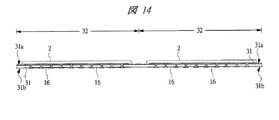
図1は、本発明の一実施の形態である半導体装置1の上面図、図2はその下面図、図3はその断面図(全体断面図)、図4はその要部断面図(部分拡大断面図)、図5はその側面図である。図1のA−A線の断面が図3にほぼ対応し、図3の端部近傍領域の拡大図が図4にほぼ対応する。また、図6は、封止樹脂5を透視したときの半導体装置1の平面透視図(上面図)であり、図7は、封止樹脂5、半導体チップ2およびボンディングワイヤ4を透視したときの半導体装置1の平面透視図(上面図)、すなわち半導体装置1に用いられている配線基板3の上面図である。なお、図7では、半導体チップ2の外形を点線で示してある。また、図7は平面図であるが、理解を簡単にするために、第1ソルダレジスト部14a、第2ソルダレジスト部14b、および第2ソルダレジスト部14bの開口部19から露出する接続端子15にハッチングを付してある。
1 is a top view of a
図1〜図7に示される本実施の形態の半導体装置1は、半導体チップ2が配線基板3に搭載(接合、接続、実装)された半導体装置(半導体パッケージ)であり、例えば、チップサイズもしくは半導体チップ2より僅かに大きい程度の小形の半導体パッケージであるCSP(Chip Size Package)形態の半導体装置である。
The
本実施の形態の半導体装置1は、半導体チップ2と、半導体チップ2を支持または搭載する配線基板3と、半導体チップ2の表面の複数の電極(第2電極、ボンディングパッド、パッド電極)2aとこれに対応する配線基板3の複数の接続端子(第1電極、ボンディングパッド、パッド電極)15とを電気的に接続する複数のボンディングワイヤ4と、半導体チップ2およびボンディングワイヤ4を含む配線基板3の上面3aを覆う封止樹脂(封止樹脂部、封止部、封止体)5と、配線基板3の下面3bに外部端子としてエリアアレイ配置で設けられた複数の半田ボール(ボール電極、突起電極、電極、外部端子)6とを有している。
The
半導体チップ2は、その厚さと交差する平面形状が正方形であり、例えば、単結晶シリコンなどからなる半導体基板(半導体ウエハ)の主面に種々の半導体素子または半導体集積回路を形成した後、必要に応じて半導体基板の裏面研削を行ってから、ダイシングなどにより半導体基板を各半導体チップ2に分離したものである。半導体チップ2は、互いに対向する表面(半導体素子形成側の主面、上面)2bおよび裏面(半導体素子形成側の主面とは逆側の主面、下面)2cを有し、その表面2bが上方を向くように配線基板3上面(チップ支持面)3a上に配置され、半導体チップ2の裏面2cが配線基板3の上面3aに接着材(ダイボンド材、接合材、接着剤)8を介して接着され固定されている。接着材8は、例えば絶縁性または導電性のペースト材などを用いることができる。接着材8の厚みは、例えば20〜30μm程度とすることができる。半導体チップ2の表面2bには、複数の電極2aが形成されており、電極2aは、半導体チップ2内部または表層部分に形成された半導体素子または半導体集積回路に電気的に接続されている。
The
配線基板3は、絶縁性の基材層(絶縁基板、コア材)11と、基材層11の上面11aおよび下面11bに形成された導体層(導体パターン、導体膜パターン、配線層)12と、基材層11の上面11aおよび下面11b上に導体層12を覆うように形成された絶縁層(絶縁体層、絶縁膜)としてのソルダレジスト層(絶縁膜、半田レジスト層)14とを有している。他の形態として、配線基板3を、複数の絶縁層と複数の配線層とを積層した多層配線基板により形成することもできる。
The
導体層12はパターン化されており、配線基板3の配線または配線層となる導体パターンである。導体層12は、導電性材料からなり、例えばめっき法で形成された銅薄膜などにより形成することができる。基材層11の上面11aの導体層12により、ボンディングワイヤ4を接続するための接続端子(電極、ボンディングパッド、パッド電極)15が複数形成され、基材層11の下面11bの導体層12により、半田ボール6を接続するための導電性のランド(電極、パッド、端子)16が複数形成されている。また、基材層11には複数の開口部(スルーホール、ビア、貫通孔)17が形成されており、各開口部17の側壁上にも導体層12が形成されている。基材層11の上面11aの接続端子15は、基材層11の上面11aの導体層12(導体層12からなる引き出し配線)、開口部17の側壁上の導体層12、および基材層11の下面11bの導体層12を介して、基材層11の下面11bのランド16に電気的に接続されている。従って、半導体チップ2の複数の電極2aは、複数のボンディングワイヤ4を介して配線基板3の複数の接続端子15に電気的に接続され、更に配線基板3の導体層12を介して配線基板3の複数のランド16に電気的に接続されている。ボンディングワイヤ4は、例えば金線などの金属細線からなる。
The
ソルダレジスト層14は、導体層12を保護する絶縁層(絶縁膜)としての機能を有しており、例えば有機系樹脂材料などの絶縁体材料からなる。また、ソルダレジスト層14は、基材層11の上面11aおよび下面11b上に導体層12を覆うように形成されており、ソルダレジスト層14が基材層11の開口部17の内部を埋めている。ソルダレジスト層14が基材層11の開口部17を埋めているので、半導体チップ2を配線基板3に接合するための接着材8が開口部17から配線基板3の下面3b側に漏れてしまうのを防止することができ、また、開口部17から半導体チップ2の裏面2cが露出してしまうのを防止することができる。また、配線基板3の導体層12のうち、接続端子15とランド16とは、ソルダレジスト層14(の開口部)から露出されている。また、基材層11の上面11aおよび下面11b上のソルダレジスト層14の厚みは、例えば20〜30μm程度とすることができる。
The solder resist
複数のランド16は、配線基板3の下面3bにアレイ状に配置されている。各ランド16の隣に開口部17が形成されている。また、各ランド16には半田ボール6が接続されている。このため、配線基板3の下面3bに複数の半田ボール6がアレイ状に配置されている。半田ボール6は、半導体装置1の外部端子として機能することができる。従って、半導体チップ2の複数の電極2aは、複数のボンディングワイヤ4を介して配線基板3の複数の接続端子15に電気的に接続され、更に配線基板3の導体層12を介して配線基板3の複数のランド16および複数のランド16に接続された複数の半田ボール6に電気的に接続されている。なお、図2の半田ボール6の数と図6,図7の接続端子15の数とは一致していないが、図1〜図7は半導体装置1の構造を模式的に示したものであり、半導体装置1における半田ボール6の数や接続端子15の数は必要に応じて種々変更可能であり、半導体装置1における半田ボール6の数と接続端子15の数とを同じにすることもでき、また異ならせることもできる。また、半導体チップ2の電極2aと電気的に接続していない半田ボール6は、放熱用に用いることもできる。
The plurality of
本実施の形態では、配線基板3の上面3aにソルダレジスト層14が形成されているが、配線基板3の上面3aのソルダレジスト層14は、半導体チップ2の下方(すなわち配線基板3の上面3aの中央部)に位置する第1ソルダレジスト部(第1の絶縁膜部)14aと、第1ソルダレジスト部14aの外周(周囲)に位置する(すなわち配線基板3の上面3aの外周部に位置する)第2ソルダレジスト部(第2の絶縁膜部)14bとを有している。第1ソルダレジスト部14aと第2ソルダレジスト部14bとの間には、ソルダレジスト層14が形成されずに基材層11が露出された領域(ダム領域)18が存在している。従って、第1ソルダレジスト部14aと第2ソルダレジスト部14bとは、領域18を挟んで離間している。領域18では、接続端子15と開口部17の側壁上の導体層12との間を接続するための引き出し配線(この引き出し配線も導体層12からなるが、図6,図7の平面図では図示を省略している)も露出している。
In the present embodiment, the solder resist
半導体チップ2は、第1ソルダレジスト部14a上に接着材8を介して接合(搭載、接続、固定、配置)されている。第2ソルダレジスト部14bは、接続端子15を露出するための開口部19を有している。図6に示されるように、接続端子15は略長方形状のパターン(導体パターン)を有しており、第2ソルダレジスト部14bの開口部19は、接続端子15用の導体パターンにオーバラップするように形成されている。このため、接続端子15の一部(両端部)上に第2ソルダレジスト部14bが重なっている。これにより、接続端子15が剥離するのをより確実に防止し、半導体装置の信頼性をより向上させることができる。
The
第2ソルダレジスト部14bの開口部19から露出する接続端子15に、ボンディングワイヤ4が接続されている。接続端子15へのボンディングワイヤ4の接続を容易または確実にするために、第2ソルダレジスト部14bの開口部19から露出する接続端子15の上面(ボンディングワイヤ4の接続面)には金めっき層(またはニッケルめっき層(下層側)と金めっき層(上層側)の積層膜)などが形成されている。また、第2ソルダレジスト部14bには、パッケージインデックスとしての開口部20aも形成されている。第2ソルダレジスト部14bに形成されたパッケージインデックスとしての開口部20aは、半導体装置1の製造工程中の位置決めや向きの認識などに用いることができる。
The
半導体チップ2は、配線基板3の上面3aの第1ソルダレジスト部14a上に接着材8を介して接合(搭載、接続、固定、配置)されているが、この第1ソルダレジスト部14aの平面寸法(面積)は、半導体チップ2の平面寸法(面積)よりも小さい。このため、半導体チップ2を搭載したとき、半導体チップ2の裏面2cの外周部(周辺部、端部近傍領域)2dの下方には、第1ソルダレジスト部14aが延在(存在)していない。従って、半導体チップ2の裏面2cの外周部2dおよび裏面2cの端部2fは、ソルダレジスト層14が形成されていない領域18上に位置することになる。また、半導体チップ2を配線基板3上にダイボンディング(接合)する際には、半導体チップ2よりも小さな寸法の第1ソルダレジスト部14a上に接着材8を配置してそこに半導体チップ2が接合されるので、半導体チップ2の裏面2cの外周部2d上には接着材8が延在(存在)しない。従って、半導体チップ2を配線基板3上にダイボンディングしたとき、半導体チップ2の裏面2cの外周部2dの下方には接着材8およびソルダレジスト層14が存在しない。すなわち、接着材8およびソルダレジスト層14(第1ソルダレジスト部14a)は半導体チップ2の側面2e(端部2f)よりも内側に存在するため、半導体チップ2の裏面2cの外周部2dは露出された状態となる。このため、半導体チップ2の裏面2cの外周部2dと配線基板3の上面3aとの間には空間(隙間)21が形成される。空間21の高さ方向の寸法(半導体チップ2の裏面2cの外周部2dと配線基板3の上面3aとの間の距離)H1は、第1ソルダレジスト部14aの厚みT1と、接着材8の厚みT2との合計にほぼ相当する(H1=T1+T2)。封止樹脂5を形成するとき(モールド工程)には、封止樹脂5を形成するための材料が半導体チップ2の裏面2cの外周部2dの下方の空間21にも充填され、硬化(固化)した封止樹脂5が半導体チップ2の裏面2cの外周部2dの下方を充填することとなり、硬化した封止樹脂5が半導体チップ2の表面2bと、半導体チップ2の側面2eと、半導体チップ2の裏面2cの外周部2dとを覆うので、半導体チップ2と封止樹脂5との密着性(接着強度)を高めることができ、半導体装置1の信頼性を向上させることができる。
The
封止樹脂5は、例えば熱硬化性樹脂材料などの樹脂材料などからなり、フィラーなどを含むこともできる。例えば、フィラーを含むエポキシ樹脂などを用いて封止樹脂5を形成することもできる。封止樹脂5は、配線基板3の上面3a上に半導体チップ2およびボンディングワイヤ4を覆うように形成されており、封止樹脂5により、半導体チップ2およびボンディングワイヤ4が封止され、保護される。
The sealing
図8は、第1の比較例の半導体装置101の要部断面図(部分拡大断面図)であり、図9は、第2の比較例の半導体装置201の要部断面図(部分拡大断面図)であり、図10は、第3の比較例の半導体装置301の要部断面図(部分拡大断面図)であり、それぞれ本実施の形態の図4に対応する領域が示されている。
FIG. 8 is a cross-sectional view (partial enlarged cross-sectional view) of the main part of the
図8に示される第1の比較例の半導体装置101では、本実施の形態とは異なり、接続端子15上を除く配線基板103の上面103aの全面にソルダレジスト層114が形成されており、半導体チップ2の裏面2cの外周部2dの下方にも、ソルダレジスト層114が延在している。このため、第1の比較例の半導体装置101では、半導体チップ2を配線基板103上にダイボンディングしたときに、ペースト材などからなる接着材8が半導体チップ2の裏面2cの端部を越えて広がり、更にソルダレジスト層114の上面上を流れて接続端子15上にまで接着材8が広がってしまう可能性がある。接続端子15上にまで接着材8が広がってしまう(流出する)と、その接続端子15へのボンディングワイヤ4の接続不良が発生しやすくなり、ボンディングワイヤ4と接続端子15との間の電気的接続の信頼性が低下する可能性がある。また、接続端子15への接着材8の流出を防止するために半導体チップ2の端部と配線基板3の接続端子15との距離を長くすることも考えられるが、これは、半導体装置の大型化(大面積化)を招いてしまう。
In the
図9に示される第2の比較例の半導体装置201では、配線基板203の上面203aに第1ソルダレジスト部214aと第2ソルダレジスト部214bとからなるソルダレジスト層214が形成されており、第1ソルダレジスト部214aと第2ソルダレジスト部214bとの間には、ソルダレジスト層214が形成されずに配線基板203の基材層11が露出した領域(ダム領域)218が存在しているが、本実施の形態とは異なり、第1ソルダレジスト部214aの平面寸法(面積)は、半導体チップ2の平面寸法(面積)よりも大きく、半導体チップ2の裏面2c全面の下方に第1ソルダレジスト部214aが延在(存在)している。第2の比較例の半導体装置201では、半導体チップ2を配線基板203上にダイボンディングしたときには、第1ソルダレジスト部214aと第2ソルダレジスト部214bとの間にソルダレジスト層214がなく基材層11が露出した領域(ダム領域)218を設けたことにより、ペースト材などからなる接着材8が領域218を越えて第2ソルダレジスト部214b上にまで広がってしまうのを防止することができる。これにより、接着材8が接続端子15上にまで広がってしまうのを防止でき、ボンディングワイヤ4と接続端子15との間の電気的接続の信頼性を向上することができる。
In the
しかしながら、図9に示される第2の比較例の半導体装置201では、第1ソルダレジスト部214aの平面寸法(面積)が半導体チップ2の平面寸法(面積)よりも大きく、半導体チップ2の裏面2c全面が接着材8を介して第1ソルダレジスト部214aに接着されている。封止樹脂5と接着材8との密着性(接着強度)は、半導体チップ2と封止樹脂5との密着性(接着強度)に比較して低い。このため、第2の比較例の半導体装置201では、封止樹脂5が半導体チップ2の表面2bおよび側面2eを覆うが、封止樹脂5は半導体チップ2の裏面2cは覆わず、半導体チップ2と封止樹脂5の接合面積が本実施の形態1(の半導体装置1)よりも小さいため、半導体チップ2と封止樹脂5との密着性(接着強度)が本実施の形態1(の半導体装置1)よりも比較的低くなる可能性がある。更には、半導体チップ2を固定するために使用される接着材8が半導体チップ2の外周部よりもはみ出した位置まで到達していると、配線基板203上の接続端子15を半導体チップ2の外周部により接近して配置することが困難であるため、本実施の形態1(の半導体装置1)に比較して半導体装置201の小型化が実現できない。
However, in the
図10に示される第3の比較例の半導体装置301では、第2の比較例の半導体装置201よりも接着材8の塗布領域や塗布量を少なくしている。これにより、半導体チップ2を配線基板203の上面203aの第1ソルダレジスト部14a上に接着材8を介して接合したときに、半導体チップ2の裏面2cの外周部2dの下方に接着材8が延在(存在)せず、半導体チップ2の裏面2cの外周部2dと配線基板203の上面203aとの間に空間(隙間)221を形成することができる。これにより、封止樹脂5を形成するときには、封止樹脂5を形成するための材料を空間221にも充填可能となり、硬化した封止樹脂5が半導体チップ2の表面2bと、半導体チップ2の側面2eと、半導体チップ2の裏面2cの外周部2dとを覆い、半導体チップ2と封止樹脂5との密着性(接着強度)を高めることができる。
In the
しかしながら、図10に示される第3の比較例の半導体装置301では、接着材8の塗布領域や塗布量を調節することにより半導体チップ2の裏面2cの外周部2dと配線基板203の上面203aとの間に空間221を形成しているので、接着材8の塗布量が少な過ぎて半導体チップ2と配線基板203の接合強度が低下したり、あるいは接着材8の塗布量が多過ぎて半導体チップ2の裏面2cの外周部2dと配線基板203の上面203aとの間に空間221を形成できない可能性がある。このため、ダイボンディング工程の管理が容易ではなく、製品ごとのばらつきが大きくなる。また、半導体チップ2よりも平面寸法(面積)が小さなダイボンドフィルムを接着材8として用いることで、半導体チップ2の裏面2cの外周部2dと配線基板203の上面203aとの間に空間221を形成することも考えられるが、ダイボンドフィルムはペースト型の接着材よりも高価であり、半導体装置の製造コストの増大を招く可能性がある。
However, in the
また、図10に示される第3の比較例の半導体装置301では、本実施の形態とは異なり、半導体チップ2の裏面2cの外周部2dの下方に第1ソルダレジスト部214aが延在しているので、半導体チップ2を配線基板203上にダイボンディングしたときに、半導体チップ2の裏面2cの外周部2dと配線基板203の上面203aとの間に形成される空間221の高さ方向の寸法H2が低く(小さく)なる。空間221の高さ方向の寸法H2は、接着材8の厚みT2にほぼ相当する(H2=T2)。接着材8の厚みが例えば20〜30μm程度であれば、空間221の高さ方向の寸法H2も20〜30μm程度となる。半導体チップ2の裏面2cの外周部2dの下方の空間221の高さ方向の寸法H2が小さいので、封止樹脂5を形成するときに、封止樹脂5を形成するための材料に含まれるフィラーなどが、半導体チップ2の裏面2cの外周部2dの下方の空間221に侵入しにくくなり、空間221を充填した封止樹脂5の成分比と、他の領域の封止樹脂5の成分比とが不均一化するなどして、硬化した封止樹脂5と半導体チップ2との密着性(接着強度)が低下する可能性がある。
In the
それに対して、本実施の形態では、配線基板3の上面3aには、その上に接着材8を介して半導体チップ2を接合する第1ソルダレジスト部(第1の絶縁膜部)14aと、第1ソルダレジスト部14aの周囲(外周)に設けられ、その開口部19から接続端子15を露出する第2ソルダレジスト部(第2の絶縁膜部)14bとが形成されている。第1ソルダレジスト部14aと第2ソルダレジスト部14bとの間には、ソルダレジスト層14が形成されずに基材層11が露出する領域(ダム領域)18が存在している。このため、半導体チップ2を配線基板3上にダイボンディングしたときには、第1ソルダレジスト部14aと第2ソルダレジスト部14bとの間にソルダレジスト層14がなく基材層11が露出した領域(ダム領域)18を設けたことにより、接着材8が領域18を越えて第2ソルダレジスト部14b上にまで広がってしまうのを防止することができる。これにより、接着材8が接続端子15上にまで広がってしまうのを防止でき、ボンディングワイヤ4と接続端子15との間の電気的接続の信頼性を向上することができる。また、たとえ流動性が比較的高いペースト型の接着材(接合材)を接着材8として用いたとしても、第1ソルダレジスト部14aと第2ソルダレジスト部14bとの間にソルダレジスト層14がない領域(ダム領域)18を設けたことにより、ペースト材からなる接着材8が接続端子15上にまで広がってしまうのを防止することができるので、ダイボンドフィルムよりも相対的に廉価なペースト型の接着材を接着材8として用いることが可能になり、半導体装置の製造コストの低減に有利である。また、配線基板3の接続端子15を半導体チップ2の外周部により接近して配置することが可能になるので、半導体装置の更なる小型化が可能になる。
On the other hand, in the present embodiment, a first solder resist portion (first insulating film portion) 14a for bonding the
更に、本実施の形態では、第1ソルダレジスト部14a上に接着材8を介して半導体チップ2が搭載され固定されているが、この第1ソルダレジスト部14aの平面寸法(面積)は、半導体チップ2の平面寸法(面積)よりも小さい。このため、半導体チップ2を配線基板3の上面3aの第1ソルダレジスト部14a上に接着材8を介して接合したときに、半導体チップ2の裏面2cの外周部2dの下方には第1ソルダレジスト部14aおよび接着材8が延在(存在)せず、半導体チップ2の裏面2cの外周部2dと配線基板3の上面3aとの間に空間21が形成される。このため、封止樹脂5を形成するときには、封止樹脂5を形成するための材料がこの空間21にも充填され、硬化した封止樹脂5が半導体チップ2の表面2bと、半導体チップ2の側面2eと、半導体チップ2の裏面2cの外周部2dとを覆うので、半導体チップ2と封止樹脂5との接合面積が増加するため、半導体チップ2と封止樹脂5との密着性(接着強度)を高めることができ、半導体装置1の信頼性を向上させることができる。本実施の形態のように、半導体チップ2の裏面2c側にも封止樹脂5を回り込ませ、半導体チップ2の裏面2cの外周部2dと配線基板3の上面3aとの間を封止樹脂5で満たす(充填する)ことにより、半導体チップ2の表面2bおよび裏面2cの両面(と側面2eと)で封止樹脂5により半導体チップ2をしっかりと封止することができ、半導体チップ2と封止樹脂5との密着性を高め、半導体チップ2と封止樹脂5との間に剥離などが生じるのをより的確に防止することができる。
Furthermore, in the present embodiment, the
更に、本実施の形態では、半導体チップ2の裏面2cの外周部2dと配線基板3の上面3aとの間に形成される空間21の高さ方向の寸法H1は、第3の比較例の半導体装置301の空間221の高さ方向の寸法H2よりも、第1ソルダレジスト部14aの厚みT1の分だけ大きくすることができる(H1>H2)。例えば、接着材8の厚みT2が20〜30μm程度で、第1ソルダレジスト部14aの厚みT1が20〜30μm程度であれば、空間21の高さ方向の寸法H1は40〜60μm程度にすることができる。このように、本実施の形態では、半導体チップ2の裏面2cの外周部2dの下方の空間21の高さ方向の寸法H1を比較的大きくすることができるので、封止樹脂5を形成するとき(モールド工程)に、封止樹脂5を形成するための材料に含まれるフィラーなどが、半導体チップ2の裏面2cの外周部2dの下方の空間21に侵入しやすく、空間21を充填した封止樹脂5の成分比と、他の領域の封止樹脂5の成分比とが均一化される。これにより、硬化した封止樹脂5と半導体チップ2との密着性(接着強度)をより向上させ、半導体装置1の信頼性をより向上することができる。
Furthermore, in the present embodiment, the dimension H 1 in the height direction of the
また、本実施の形態では、第2ソルダレジスト部14bの内周部(第1ソルダレジスト部14aに対向する第2ソルダレジスト部14bの内周部、半導体チップ2の四辺に対向する第2ソルダレジスト部14bの内周部)の角部(四隅、コーナー部)では、第2ソルダレジスト部14bのパターンを半導体装置1の外周方向に(すなわち半導体チップ2から遠ざかる方向に)後退させている。すなわち、第2ソルダレジスト部14bの内周部の角部(四隅)に、ソルダレジストが形成されずに基材層11が露出したソルダレジスト後退部20bを設けている。
In the present embodiment, the inner periphery of the second solder resist
第2ソルダレジスト部14bの内周部の角部(四隅)で第2ソルダレジスト部14bのパターンを後退させる(すなわちソルダレジスト後退部20bを設ける)ことで、封止樹脂5をトランスファモールド工程などによって形成する際に、半導体チップ2の裏面2cの外周部2dと配線基板3の上面3aとの間の空間21から空気が抜けやすくなり、封止樹脂5を形成するための材料の流動性が向上し、上記空間21への封止樹脂の充填性をより向上させることができる。このため、半導体チップ2と封止樹脂5との密着性(接着強度)をより向上させることができ、半導体装置1の信頼性をより向上させることができる。
By retreating the pattern of the second solder resist
図11は、他の形態の半導体装置1aの要部断面図であり、図12は、その平面透視図(上面図)である。図11は、上記図4に対応する。また、図12は、上記図7に対応し、封止樹脂5、半導体チップ2およびボンディングワイヤ4を透視したときの半導体装置1aの平面透視図(上面図)、すなわち半導体装置1aに用いられている配線基板3の上面図が示されている。なお、図12では、半導体チップ2の外形を点線で示してある。また、図12は平面図であるが、理解を簡単にするために、第1ソルダレジスト部14a、第2ソルダレジスト部14b、および第2ソルダレジスト部14bの開口部19から露出する接続端子15にハッチングを付してある。
FIG. 11 is a cross-sectional view of an essential part of another form of semiconductor device 1a, and FIG. 12 is a plan perspective view (top view) thereof. FIG. 11 corresponds to FIG. FIG. 12 corresponds to FIG. 7 described above, and is used in the planar perspective view (top view) of the semiconductor device 1a when the sealing
上記半導体装置1では、半導体チップ2の裏面2cの端部2f(半導体チップ2の側面2e)は、ソルダレジスト層14が形成されずに基材層11が露出する領域(ダム領域)18上に位置していたが、図11および図12に示される半導体装置1aでは、半導体チップ2の裏面2cの端部2f(半導体チップ2の側面2e)は、第2ソルダレジスト部14b上に位置している。半導体装置1aの他の構成は上記半導体装置1とほぼ同様である。
In the
半導体装置1aも半導体装置1とほぼ同様の効果を得ることができ、本発明の半導体装置に含むものとする。ただし、半導体装置1のように半導体チップ2の裏面2cの端部2f(半導体チップ2の側面2e)が領域(ダム領域)18上に位置している場合の方が、半導体装置1aのように半導体チップ2の裏面2cの端部2f(半導体チップ2の側面2e)が第2ソルダレジスト部14b上に位置している場合よりも、半導体チップ2を配線基板3の上面3aにダイボンディングしたときに半導体チップ2の裏面2cの外周部2dと配線基板3の上面3aとの間に形成される空間21をより広くすることができ、封止樹脂5を形成するときにフィラーなどが半導体チップ2の裏面2cの外周部2dの下方の空間21に侵入しやすくなるので、空間21を満たす封止樹脂5の成分比と、他の領域の封止樹脂5の成分比とをより均一にすることができる。このため、半導体装置1は、封止樹脂5と半導体チップ2との密着性(接着強度)向上や信頼性の向上により有利である。一方、半導体装置1aのように半導体チップ2の裏面2cの端部2f(半導体チップ2の側面2e)の下方に第2ソルダレジスト部14bを延在させることで、接続端子15を半導体チップ2側により近づけることが可能になる。このため、半導体装置1aは、小型化(小面積化)により有利である。
The semiconductor device 1a can obtain substantially the same effect as the
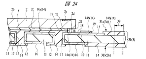
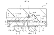
次に、本実施の形態の半導体装置の製造方法を、図面を参照して説明する。図13〜図20は、本実施の形態の半導体装置の製造工程中の断面図である。図21〜図23は、本実施の形態の半導体装置1の製造に用いられる配線基板31の製造工程の一例を模式的に示す平面図(上面図)である。図24は、本実施の形態の半導体装置の製造工程中の要部断面図であり、図14と同じ工程段階(ダイボンディング工程)に対応する。図25は、本実施の形態の半導体装置の製造工程中の平面図(上面図)であり、図15と同じ工程段階に対応する。図26,図27は、ワイヤボンディング工程の説明図(要部断面図)である。図28は、本実施の形態の半導体装置の製造工程中の要部断面図であり、図16と同じ工程段階(モールド工程)に対応する。また、図21〜図28には、後述する切断工程で配線基板31を切断するダイシング領域(ダイシングライン)39も示してある。
Next, a method for manufacturing the semiconductor device of the present embodiment will be described with reference to the drawings. 13 to 20 are cross-sectional views during the manufacturing process of the semiconductor device of the present embodiment. 21 to 23 are plan views (top views) schematically showing an example of a manufacturing process of the
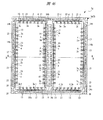
なお、本実施の形態では、複数の配線基板3がアレイ状に繋がって形成された多数個取りの配線基板(配線基板母体)31を用いて個々の半導体装置1を製造する場合について説明する。この配線基板31は、上記配線基板3の母体であり、配線基板31を後述する切断工程で切断し、各半導体装置領域(基板領域、単位基板領域)32に分離したものが半導体装置1の配線基板3に対応する。配線基板31は、そこから1つの半導体装置1が形成される領域である半導体装置領域(基板領域、単位基板領域)32がマトリクス状に複数配列した構成を有している。
In the present embodiment, a case will be described in which
まず、配線基板31を準備する。配線基板31は例えば次のようにして製造することができる。
First, the
コア材としての絶縁性の基材層11の上面11aおよび下面上に無電解めっき(無電界めっき)法により無電解銅めっき層を形成し、この無電解銅めっき層をエッチングなどによりパターニングする。それから、無電解銅めっき層上に電解めっき(電界めっき)法により電解銅めっき層を形成し、銅層の厚みを厚くする。この無電解銅めっき層および電解銅めっき層の積層膜(銅層)によって、上記導体層12を形成することができる。図21には、スルーホール用の導体パターン33と接続端子15(用の導体パターン)とが、基材層11の上面に、無電解銅めっき層および電解銅めっき層の積層膜(導体層12)によって形成された状態が示されている。接続端子15と導体パターン33とは、基材層11の上面11aに形成された無電解銅めっき層および電解銅めっき層の積層膜(導体層12)からなる引き出し配線(図示省略)によって電気的に接続されている。また、図示はしないけれども、基材層11の下面には、ランド16も、無電解銅めっき層および電解銅めっき層の積層膜によって形成されている。また、電解めっき法を用いるので、基材層11の上面11aには、めっき配線(給電線)34も形成されており、このめっき配線34を介して所定の電位(電力)を供給して、無電解銅めっき層上に電解銅めっき層を形成することができる。
An electroless copper plating layer is formed on the
次に、図22に示されるように、基材層11に開口部(スルーホール、ビア、貫通孔)17を形成する。開口部17は、スルーホール用の導体パターン33の内側に形成される。
Next, as shown in FIG. 22, openings (through holes, vias, through holes) 17 are formed in the
次に、無電解めっき法により開口部17の側壁上に無電解銅めっき層を形成する。この基材層11の開口部17の側壁上に形成された無電解銅めっき層が、開口部17の側壁上に形成された上記導体層12となる。それから、図23に示されるように、印刷法などを用いてソルダレジスト層14を基材層11の上面11aおよび下面上に開口部17内を埋めるように形成する。これにより、基材層11の上面11aには、第1ソルダレジスト部14aと第2ソルダレジスト部14bが形成される。基材層11の上面11aでは、接続端子15がソルダレジスト層14(第2ソルダレジスト部14b)の開口部から露出し、基材層11の下面では、ランド16がソルダレジスト層14の開口部から露出する。次に、基材層11の上面11aおよび下面上の銅めっき層の露出部(すなわち接続端子15およびランド16)上に、ニッケルめっき層および金めっき層を電解めっき法により順に形成する。その後、必要に応じて基材層11を外形加工(切断)して配線基板31を形成することができる。このようにして準備された配線基板31は、後述する配線基板31の切断工程で分割されて配線基板3となる半導体装置領域(基板領域、単位基板領域)32を複数有しており、配線基板31の上面31aの各半導体装置領域32に形成された第1ソルダレジスト部14aと、この第1ソルダレジスト部14aの外周に形成された第2ソルダレジスト部14bとを有している。
Next, an electroless copper plating layer is formed on the sidewall of the
上記のようにして準備(製造)された配線基板31の上面31aの各半導体装置領域32上に、図14および図24に示されるように、半導体チップ2を接着材8を介して接合(ダイボンディング、チップマウント)する。このダイボンディング工程では、例えば、配線基板31の上面31aの各半導体装置領域32の第1ソルダレジスト部14a上に熱硬化性の接着材8を塗布してチップ固定用の接着層を第1ソルダレジスト部14a上に形成し、接着材8上に半導体チップ2を載置し、加熱などにより接着材8を硬化して、半導体チップ2の裏面2cと第1ソルダレジスト部14aとを接着材8を介して接合する。半導体チップ2のダイボンディング工程では、上記のように、半導体チップ2よりも平面寸法(面積)が小さな第1ソルダレジスト部14a上に接着材8を介して半導体チップ2を接合しているので、半導体チップ2の裏面2cの外周部2dの下方にはソルダレジスト層14(第1ソルダレジスト部14aおよび第2ソルダレジスト部14b)や接着材8が延在(存在)しない。このため、半導体チップ2を配線基板31の各半導体装置領域32上に接合したときに、半導体チップ2の裏面2cの外周部2dと配線基板3の上面3aとの間に空間21が形成され、この空間21の高さ方向の寸法H1は、第1ソルダレジスト部14aの厚みT1と、接着材8の厚みT2との合計にほぼ相当する(H1=T1+T2)ものになり、空間21の高さ方向の寸法H1を比較的大きくすることができる。例えば、接着材8の厚みT2が20〜30μm程度で、第1ソルダレジスト部14aの厚みT1が20〜30μm程度であれば、空間21の高さ方向の寸法H1は40〜60μm程度にすることができる。
As shown in FIGS. 14 and 24, the
次に、図15および図25に示されるように、ワイヤボンディング工程を行って、半導体チップ2の各電極2aと、これに対応する配線基板31に形成された接続端子15とをボンディングワイヤ4を介して電気的に接続する。すなわち、配線基板31の上面31aの各半導体装置領域32上の複数の接続端子15とその半導体装置領域32上に接合された半導体チップ2の複数の電極2aとを複数のボンディングワイヤ4を介して電気的に接続する。例えば、ワイヤボンディング装置を用い、半導体チップ2の電極2aにボンディングワイヤ4の一端を接続(ファーストボンディング)してから、配線基板31の接続端子15にボンディングワイヤ4の他端を接続(セカンドボンディング)する。
Next, as shown in FIGS. 15 and 25, a wire bonding process is performed to connect each
このワイヤボンディング工程においては、他の形態として、図26の要部断面図に示されるように、まず配線基板31の接続端子15に金(Au)などからなるスタッドバンプ(バンプ電極、バンプ)35を形成した後、図27に示されるように、半導体チップ2の電極2aにボンディングワイヤ4の一端を接続してから、配線基板31の接続端子15上に形成したスタッドバンプ35にボンディングワイヤ4の他端を接続することもできる。接続端子15を半導体チップ2に比較的近い位置に形成し、あるいは比較的厚い半導体チップ2を用いるなどして、ボンディングワイヤ4と接続端子15とが為す角度が急に(例えば垂直に近く)なり、ボンディングワイヤ4に対する折り曲げストレスが大きくなったとしても、接続端子15上にスタッドバンプ35を形成し、このスタッドバンプ35にボンディングワイヤ4を接続したことによりボンディングワイヤ4と接続端子15(スタッドバンプ35)との間の接続強度を向上でき、ボンディングワイヤ4の接続端子15(スタッドバンプ35)からの剥がれを抑制または防止することができる。このため、接続端子15から半導体チップ2までの距離を小さくすることができ、半導体装置1の平面寸法を低減することが可能になる。また、厚みが比較的厚い半導体チップ2の使用も可能になり、半導体チップ2に対する選択の幅を広くすることができる。
In this wire bonding step, as another form, as shown in the cross-sectional view of the main part of FIG. 26, first, a stud bump (bump electrode, bump) 35 made of gold (Au) or the like is formed on the
ワイヤボンディング工程の後、図16および図28に示されるように、モールド工程(例えばトランスファモールド工程)による樹脂封止を行って封止樹脂5a(封止部)を形成し、半導体チップ2およびボンディングワイヤ4を封止樹脂5aによって封止する。このモールド工程では、配線基板31の上面31aの複数の半導体装置領域32を封止樹脂5aで一括して封止する一括封止を行う。すなわち、配線基板31の上面31aの複数の半導体装置領域32上に半導体チップ2およびボンディングワイヤ4を覆うように封止樹脂5aを形成する。このため、封止樹脂5aは、配線基板31の上面31aの複数の半導体装置領域32を覆うように形成される。封止樹脂5aは、例えば熱硬化性樹脂材料などの樹脂材料などからなり、フィラーなどを含むこともできる。例えば、フィラーを含むエポキシ樹脂などを用いて封止樹脂5aを形成することができる。
After the wire bonding step, as shown in FIGS. 16 and 28, resin sealing is performed by a molding step (for example, transfer molding step) to form a sealing
このモールド工程では、封止樹脂5aを形成するための材料は、半導体チップ2の裏面2cの外周部2dの下方の空間21にも充填される。本実施の形態では、半導体チップ2の裏面2cの外周部2dの下方の空間21の高さ方向の寸法H1が比較的大きいので、モールド工程で、封止樹脂5aを形成するための材料に含まれるフィラーなどが、半導体チップ2の裏面2cの外周部2dの下方の空間21に侵入しやすく、空間21を満たした(充填した)封止樹脂5aの成分比と、他の領域の封止樹脂5aの成分比とが均一化されるので、硬化した封止樹脂5aと半導体チップ2との密着性(接着強度)をより向上させることができる。
In this molding step, the material for forming the sealing
次に、図17に示されるように、配線基板31の下面31bのランド16に半田ボール6を接続(接合)する。例えば、配線基板31の下面31bを上方に向け、配線基板31の下面31bの複数のランド16上に複数の半田ボール6を配置してフラックスなどで仮固定し、リフロー処理(半田リフロー処理、熱処理)を行って半田を溶融し、半田ボール6と配線基板31の下面31bのランド16とを接合することができる。その後、必要に応じて洗浄工程を行い、半田ボール6の表面に付着したフラックスなどを取り除くこともできる。このようにして、半導体装置1の外部端子としての半田ボール6が接合される。なお、本実施の形態では、半導体装置1の外部端子として半田ボール6を接合する場合について説明したが、これに限定されるものではなく、例えば半田ボール6の代わりに印刷法などによりランド16上に半田を供給して半導体装置1の外部端子(バンプ電極)を形成することもできる。また、半導体装置1はBGA(Ball Grid Array)形態の半導体装置として説明したが、これに限定されるものではなく、半田ボール6の形成を省略し、半導体装置1をLGA(Land Grid Array)形態の半導体装置とすることもできる。また、半導体装置1の外部端子(ここでは半田ボール6)の材質は、鉛含有半田や鉛を含有しない鉛フリー半田を用いることができ、また、めっき(例えば金めっきやPdめっきなど)により半導体装置1の外部端子(バンプ電極)を形成することもできる。
Next, as shown in FIG. 17, the
次に、図18に示されるように、マーキングを行って、封止樹脂5aの表面に製品番号などのマークを付す。例えば、レーザ36によりマーキングを行うレーザマークを行うことができるが、インクによりマーキングを行うインクマークを行うこともできる。また、図17の半田ボール6の接続工程と図18のマーキング工程の順番を入れ換え、図18のマーキング工程を行った後に、図17の半田ボール6の接続工程を行うこともできる。
Next, as shown in FIG. 18, marking is performed, and a mark such as a product number is attached to the surface of the sealing
次に、図19に示されるように、封止樹脂5aの上面をパッケージ固定テープ37に貼り付け、配線基板31およびその上に形成された封止樹脂5aをダイシング領域(ダイシングライン)39に沿ってダイシングブレード38などにより切断(ダイシング)して、それぞれの半導体装置領域(CSP領域)を個々の(個片化された)半導体装置1(CSP)に切断分離する。すなわち、配線基板31および封止樹脂5aを各半導体装置領域32に切断して分割する。このように、切断・個片化を行って、図1〜図7に示されるような半導体装置1を製造することができる。各半導体装置領域32に切断され分離(分割)された配線基板31が配線基板3に対応し、各半導体装置領域32に切断され分離(分割)された封止樹脂5aが封止樹脂5に対応する。
Next, as shown in FIG. 19, the upper surface of the sealing
図29は、上記のようにして製造された半導体装置1の端部近傍領域の他の要部断面図(部分拡大断面図)であり、図4とは異なる領域の断面が示されている。上記のように、配線基板3(配線基板31)の導体層12を電解めっき法を用いて形成しているので、配線基板3を構成する基材層11の上面11a周辺部(基材層11の上面11aの端部と接続端子15との間)には、めっき配線34が存在している。本実施の形態では、このめっき配線34上はソルダレジスト層14(第2ソルダレジスト部14b)で覆われており、めっき配線34と封止樹脂5とは接触しないようになっている。
FIG. 29 is a cross-sectional view (partially enlarged cross-sectional view) of another main portion of the region near the end of the
本実施の形態とは異なり、めっき配線34上にソルダレジスト層14が形成されていない場合、接続端子15上に金めっき層を形成した際に、めっき配線34上にも金めっき層が形成され、封止樹脂5(封止樹脂5a)を形成した際には、上面に金めっき層が形成されためっき配線34と封止樹脂5とが直接接触してしまう。この場合、封止樹脂5と電解金めっき層の密着性はソルダレジスト層14と封止樹脂5との密着性よりも低いため、めっき配線34と封止樹脂5における密着性が低下する。この密着性が低い界面(めっき配線34と封止樹脂5との界面)は個片化後に半導体装置の側面で露出するので、その界面から湿気(水分)が進入する吸湿不良を引き起こす。この吸湿不良により封止樹脂5の密着性の低下による剥離や、湿気によるボンディングワイヤ4の錆や酸化が生じ、半導体装置の信頼性が低下する可能性がある。
Unlike the present embodiment, when the solder resist
本実施の形態では、配線基板3(配線基板31)の導体層12を電解めっき法を用いて形成した場合には、めっき配線34上をソルダレジスト層14(第2ソルダレジスト部14b)で覆うことで、めっき配線34と封止樹脂5とが接触しないようにし、密着性が低い界面が半導体装置の側面に形成されないようにするので、半導体装置の側面からの吸湿不良を抑制し、半導体装置の信頼性を向上させることができる。
In the present embodiment, when the
(実施の形態2)
図30は、本発明の他の実施の形態である半導体装置1bの製造工程中の要部断面図であり、上記実施の形態1の図4にほぼ対応する領域が示されている。図31および図32は、本実施の形態のワイヤボンディング工程の説明図(要部断面図)である。
(Embodiment 2)
FIG. 30 is a fragmentary cross-sectional view of the semiconductor device 1b according to another embodiment of the present invention during the manufacturing process, and shows a region substantially corresponding to FIG. 4 of the first embodiment. FIG. 31 and FIG. 32 are explanatory diagrams (main-part sectional views) of the wire bonding step of the present embodiment.
本実施の形態の半導体装置1bの製造工程は、ワイヤボンディング工程以外は上記実施の形態1とほぼ同様であるのでここではその説明は省略し、本実施の形態の半導体装置1bの製造工程におけるワイヤボンディング工程について説明する。 The manufacturing process of the semiconductor device 1b according to the present embodiment is almost the same as that of the first embodiment except for the wire bonding process, so that the description thereof is omitted here, and the wire in the manufacturing process of the semiconductor device 1b according to the present embodiment is omitted. The bonding process will be described.
上記実施の形態1では、先に半導体チップ2の電極2aにボンディングワイヤ4の一端を接続(ファーストボンディング)してから、配線基板31の接続端子15にボンディングワイヤ4の他端を接続(セカンドボンディング)しているが、本実施の形態では、先に配線基板31の接続端子15にボンディングワイヤ4の一端を接続(ファーストボンディング)してから、半導体チップ2の電極2aにボンディングワイヤ4の他端を接続(セカンドボンディング)している。
In
すなわち、まず、図31に示されるように、ボンディングワイヤ4形成用のワイヤボンディング装置のキャピラリ41に保持された金(Au)などからなるボンディングワイヤ4の先端を超音波を印加しながら配線基板31の接続端子15表面に押し付けて接続する。それから、図32に示されるように、キャピラリ41を上方に引き上げてから横方向に移動させ、ボンディングワイヤ4を半導体チップ2の電極2aの表面に超音波を印加しながらこすりつけて接続してからボンディングワイヤ4を切断する。これにより、配線基板31の接続端子15と半導体チップ2の電極2aとをボンディングワイヤ4を介して電気的に接続することができる。このようにしてワイヤボンディングを行うことで、図30に示される半導体装置1bを製造することができる。
That is, first, as shown in FIG. 31, the
図33は、本実施の形態とは異なり、先に半導体チップ2の電極2aにボンディングワイヤ4の一端を接続(ファーストボンディング)してから、配線基板31の接続端子15にボンディングワイヤ4の他端を接続(セカンドボンディング)する様子を示す要部断面図である。図33に示されるように、先に半導体チップ2の電極2aにボンディングワイヤ4の一端を接続する場合は、セカンドボンディングを行うためにキャピラリ41を接続端子15上に移動するときにキャピラリ41と半導体チップ2との間にボンディングワイヤ4が位置することになる。このため、配線基板31の接続端子15を半導体チップ2に近づけ過ぎると、ボンディングワイヤ4が半導体チップ2と接触してしまう可能性がある。
FIG. 33 differs from the present embodiment in that one end of the
それに対して、本実施の形態では、図31および図32に示されるように、先に配線基板31の接続端子15にボンディングワイヤ4の一端を接続(ファーストボンディング)してから、半導体チップ2の電極2aにボンディングワイヤ4の他端を接続(セカンドボンディング)している。すなわち、配線基板31の接続端子15へのファーストボンディングを行った後、キャピラリ41を上方に引き上げてから横方向に移動させ、半導体チップ2の電極2aへのセカンドボンディングを行うことができる。このため、セカンドボンディングを行うためにキャピラリ41を半導体チップ2の電極2a上に移動するときに、キャピラリ41と半導体チップ2との間にボンディングワイヤ4が位置しない。従って、配線基板31の接続端子15を半導体チップ2に近づけても、ボンディングワイヤ4が半導体チップ2と接触してしまうのを防止することができる。これにより、半導体装置の信頼性を高めることができる。また、配線基板31の接続端子15を半導体チップ2により近づけることが可能になるので、半導体装置を小型化(小面積化)することができる。
On the other hand, in the present embodiment, as shown in FIGS. 31 and 32, one end of the
また、ワイヤボンディング工程では、セカンドボンディングに比較してファーストボンディングの方が、接続に要する電極面積を小さくすることができる。本実施の形態では、先に配線基板31の接続端子15にボンディングワイヤ4の一端を接続(ファーストボンディング)することにより、接続端子15の面積を小さくすることが可能になり、第2ソルダレジスト部14bの接続端子15露出用の開口部19を小さくすることができる。すなわち、キャピラリ41に保持されたボンディングワイヤ4の先端を超音波を印加しながら配線基板31の接続端子15表面に押し付けて接続(ファーストボンディング)してから、キャピラリ41を上方に引き上げるので、接続端子15を小さくすることができ、第2ソルダレジスト部14bの接続端子15露出用の開口部19を小さくすることができる。例えば、接続端子15の長さ(接続端子15の延在方向の長さ)L1、すなわち第2ソルダレジスト部14bの接続端子15露出用の開口部19の長さL1を、好ましくは120μm以下(L1≦120μm)、より好ましくは100μm以下(L1≦100μm)にすることができる。これにより、半導体装置の小型化(小面積化)が可能になる。
Further, in the wire bonding process, the first bonding can reduce the electrode area required for connection compared to the second bonding. In the present embodiment, by connecting one end of the
また、図31および図32の要部断面図に示されるように、半導体チップ2の電極2aに金(Au)などからなるスタッドバンプ(バンプ電極、バンプ)42を形成しておき、セカンドボンディングの際には、半導体チップ2の電極2a上のスタッドバンプ42にボンディングワイヤ4を接続すれば、より好ましい。これにより、ボンディングワイヤ4と半導体チップ2の電極2aとの接続強度を向上することができる。また、半導体チップ2の電極2aへのセカンドボンディングの際に半導体チップ2に与えられるストレスを低減することができる。
31 and 32, stud bumps (bump electrodes, bumps) 42 made of gold (Au) or the like are formed on the
さらには、ボンディングワイヤ4と半導体チップ2(半導体チップの表面側における端部2f)との距離が大きく取れるので、半導体チップ2の裏面2c側への封止樹脂5の流動性が、図33に示すようにワイヤボンディングする場合よりも向上できる。
Furthermore, since the distance between the
(実施の形態3)
図34は、本発明の他の実施の形態である半導体装置1cの要部断面図であり、図35は、その平面透視図(上面図)である。図34は、上記実施の形態1の図4に対応する。また、図35は、上記実施の形態1の図7に対応し、封止樹脂5、半導体チップ2およびボンディングワイヤ4を透視したときの半導体装置1cの平面透視図(上面図)、すなわち半導体装置1cに用いられている配線基板3の上面図が示されている。なお、図35では、半導体チップ2の外形を点線で示してある。また、図35は平面図であるが、理解を簡単にするために、第1ソルダレジスト部14a、第2ソルダレジスト部14b、第3ソルダレジスト部14c、および第2ソルダレジスト部14bの開口部19から露出する接続端子15にハッチングを付してある。
(Embodiment 3)
FIG. 34 is a fragmentary cross-sectional view of a
本実施の形態の半導体装置1cは、配線基板3の上面3aに形成されたソルダレジスト層14以外の構成は、上記実施の形態1の半導体装置1とほぼ同様であるのでここではその説明は省略し、半導体装置1cにおける配線基板3の上面3aに形成されたソルダレジスト層14について説明する。
The
上記実施の形態1では、配線基板3の上面3aのソルダレジスト層14は、半導体チップ2の下方に位置する第1ソルダレジスト部14aと、配線基板3の上面3aの外周部上に位置する第2ソルダレジスト部14bとによって構成されていたが、本実施の形態の半導体装置1cでは、配線基板3の上面3aのソルダレジスト層14は、図34および図35に示されるように、半導体チップ2の下方に位置する第1ソルダレジスト部14aと、配線基板3の上面3aの外周部上に位置する第2ソルダレジスト部14bと、更に、第1ソルダレジスト部14aと第2ソルダレジスト部14bとの間に第1ソルダレジスト部14aを囲むように形成された第3ソルダレジスト部14cとを有している。第1ソルダレジスト部14aと第3ソルダレジスト部14cとの間には、ソルダレジスト層14が形成されずに基材層11(および導体層12からなる引き出し配線)が露出された領域(ダム領域)18aが存在し、第3ソルダレジスト部14cと第2ソルダレジスト部14bとの間には、ソルダレジスト層14が形成されずに基材層11(および導体層12からなる引き出し配線)が露出された領域(ダム領域)18bが存在している。第1ソルダレジスト部14a上に接着材8を介して半導体チップ2が接合(搭載、接続、固定、配置)されている。第2ソルダレジスト部14bは、接続端子15を露出するための開口部19を有している。上記実施の形態1と同様に、第1ソルダレジスト部14aの平面寸法(面積)は、半導体チップ2の平面寸法(面積)よりも小さい。このため、半導体チップ2を搭載したとき、半導体チップ2の裏面2cの外周部2dの下方には、第1ソルダレジスト部14aが延在(存在)しない。
In the first embodiment, the solder resist
このように、本実施の形態では、配線基板3の上面3aには、その上に接着材8を介して半導体チップ2を接合する第1ソルダレジスト部14aと、第1ソルダレジスト部14aの周囲(外周)に設けられた第3ソルダレジスト部14cと、第3ソルダレジスト部14cの周囲(外周)に設けられてその開口部19から接続端子15を露出する第2ソルダレジスト部14bとが形成されている。第1ソルダレジスト部14aと第3ソルダレジスト部14cとの間および第3ソルダレジスト部14cと第2ソルダレジスト部14bとの間には、ソルダレジスト層14が形成されずに基材層11が露出する領域(ダム領域)18a,18bが存在している。このため、半導体チップ2を配線基板3上にダイボンディングしたときには、第1ソルダレジスト部14aと第3ソルダレジスト部14cとの間にソルダレジスト層14がなく基材層11が露出した領域(ダム領域)18aを設けたことにより、ペースト材などからなる接着材8が領域18aを越えて第3ソルダレジスト部14c上にまで広がってしまうのを防止し、更に、たとえペースト材などからなる接着材8が領域18aを越えて第3ソルダレジスト部14c上にまで広がったとしても、第3ソルダレジスト部14cと第2ソルダレジスト部14bとの間にソルダレジスト層14がなく基材層11が露出した領域(ダム領域)18bを設けたことにより、ペースト材などからなる接着材8が領域18bを越えて第2ソルダレジスト部14b上にまで広がってしまうのを防止することができる。これにより、接着材8が接続端子15上にまで広がってしまうのをより確実に防止でき、ボンディングワイヤ4と接続端子15との間の電気的接続の信頼性をより的確に向上することができる。また、たとえ流動性が比較的高いペースト型の接着材(接合材)を接着材8として用いたとしても、ペースト材からなる接着材8が接合端子15上にまで広がってしまうのを防止することができるので、ダイボンドフィルムよりも相対的に廉価なペースト型の接着材を接着材8として用いることが可能になり、半導体装置の製造コストの低減に有利である。
As described above, in the present embodiment, the
(実施の形態4)
図36は、本発明の他の実施の形態である半導体装置1dの要部断面図であり、上記実施の形態1の図4に対応する。
(Embodiment 4)
FIG. 36 is a main-portion cross-sectional view of the semiconductor device 1d according to another embodiment of the present invention, and corresponds to FIG. 4 of the above-described first embodiment.
上記実施の形態1では、半導体装置1の配線基板3の上面3aの第1ソルダレジスト部14aの厚みと第2ソルダレジスト部14bとの厚みとは、ほぼ同じ厚みであったが、本実施の形態の半導体装置1dでは、配線基板3の上面3aの第1ソルダレジスト部14aの厚みT1が第2ソルダレジスト部14bの厚みT3よりも厚く(T1>T3)なっている。他の構成は上記実施の形態1とほぼ同様であるので、ここではその説明は省略する。
In the first embodiment, the thickness of the first solder resist
本実施の形態では、図36に示されるように、半導体チップ2よりも平面寸法が小さく、その上に接着材8を介して半導体チップ2を接合する第1ソルダレジスト部14aの厚みをT1を、第1ソルダレジスト部14aの周囲(外周)に設けられた第2ソルダレジスト部14bの厚みT3よりも厚く(T1>T3)している。このような配線基板3は、例えば、基材層11の上面11aにソルダレジスト層14を形成する際に、ソルダレジスト層を2度塗り(複数塗り、複数印刷)し、第2ソルダレジスト部14bは1層目のソルダレジスト層によって形成することで相対的に薄くし、第1ソルダレジスト部14aは1層目および2層目のソルダレジスト層(の積層膜)によって形成することで相対的に厚くすることで、準備(製造)することができる。
In the present embodiment, as shown in FIG. 36, the planar dimension is smaller than that of the
本実施の形態では、第1ソルダレジスト部14aの厚みT1を第2ソルダレジスト部14bの厚みT3よりも厚く(T1>T3)しているので、第1ソルダレジスト部14aの厚みT1と第2ソルダレジスト部14bの厚みT3とが同じ(T1=T3)場合に比較して、配線基板3上に半導体チップ2をダイボンディングしたときに半導体チップ2の裏面2cの外周部2dと配線基板3の上面3aとの間に形成される空間21の高さ方向の寸法H1をより大きくすることができる。このため、封止樹脂5を形成するときに、封止樹脂5を形成するための材料に含まれるフィラーなどが、半導体チップ2の裏面2cの外周部2dの下方の空間21により侵入しやすくなり、空間21を充填した封止樹脂5の成分比と、他の領域の封止樹脂5の成分比とをより均一化することができる。これにより、硬化した封止樹脂5と半導体チップ2との密着性(接着強度)をより向上させ、半導体装置1dの信頼性をより向上することができる。
In this embodiment, since the thickness T 1 of the first solder resist
(実施の形態5)
図37は、本発明の他の実施の形態である半導体装置の平面透視図(上面図)であり、図38は、本発明の更に他の実施の形態である半導体装置の平面透視図(上面図)であり、それぞれ上記実施の形態1の図7に対応する。従って図37および図38には、封止樹脂5、半導体チップ2およびボンディングワイヤ4を透視したときの半導体装置の平面透視図(上面図)、すなわち、本実施の形態の半導体装置に用いられている配線基板3の上面図が示されている。また、図37および図38では、半導体チップ2の外形を点線で示してある。また、図37および図38は平面図であるが、理解を簡単にするために、第1ソルダレジスト部14a、第2ソルダレジスト部14b、および第2ソルダレジスト部14bの開口部19から露出する接続端子15にハッチングを付してある。
(Embodiment 5)
FIG. 37 is a plan perspective view (top view) of a semiconductor device according to another embodiment of the present invention, and FIG. 38 is a plan perspective view (top view) of a semiconductor device according to still another embodiment of the present invention. And corresponds to FIG. 7 of the first embodiment. Therefore, in FIGS. 37 and 38, a plan perspective view (top view) of the semiconductor device when the sealing
本実施の形態の半導体装置は、配線基板3の上面3aに形成された第2ソルダレジスト部14bのパターン形状以外の構成は、上記実施の形態1の半導体装置1とほぼ同様であるのでここではその説明は省略し、本実施の形態の半導体装置における配線基板3の上面3aに形成された第2ソルダレジスト部14bのパターン形状について説明する。
The configuration of the semiconductor device of the present embodiment is substantially the same as that of the
本実施の形態では、第2ソルダレジスト部14bの内周部(第1ソルダレジスト部14aに対向する第2ソルダレジスト部14bの四辺、半導体チップ2の四辺に対向する第2ソルダレジスト部14bの四辺)には、櫛歯状(凹凸状)のパターンが形成されている。すなわち、第2ソルダレジスト部14bは、配線基板3の上面3aの外周部上に形成され、接続端子15を露出するための開口部19を有する第1の部分61と、第1の部分61に接続し、第1の部分61から第1ソルダレジスト部14a(半導体チップ2)に近づく方向に延在する複数の第2の部分62とを有している。櫛歯状のパターンを含む第2ソルダレジスト部14b全体の膜厚はほぼ均一である。
In the present embodiment, the inner periphery of the second solder resist
第2ソルダレジスト部14bを第1の部分61と複数の第2の部分62とにより形成し、第2ソルダレジスト部14bの内周の四辺に櫛歯状のパターン(ソルダレジストパターン)を設けることで、封止樹脂5をトランスファモールド工程などによって形成する際に、半導体チップ2の裏面2cの外周部2dと配線基板3の上面3aとの間の空間21から空気が抜けやすくなり、封止樹脂5を形成するための材料の流動性が向上し、上記空間21への封止樹脂の充填性をより向上させることができる。このため、半導体チップ2と封止樹脂5との密着性(接着強度)をより向上させることができ、半導体装置の信頼性をより向上させることができる。
The second solder resist
また、図37のように、第2ソルダレジスト部14bの第2の部分62が半導体チップ2の下方まで延在していなければ、半導体チップ2を配線基板3の上面3aにダイボンディングしたときに半導体チップ2の裏面2cの外周部2dと配線基板3の上面3aとの間に形成される空間21をより広くすることができ、封止樹脂5を形成するときにフィラーなどが半導体チップ2の裏面2cの外周部2dの下方の空間21に侵入しやすくすることができる。これにより、空間21を満たす封止樹脂5の成分比と、他の領域の封止樹脂5の成分比とをより均一にすることができる。また、図38のように第2ソルダレジスト部14bの第2の部分62を半導体チップ2の下方まで延在させることもでき、この場合、接続端子15を半導体チップ2側により近づけることが可能になり、半導体装置の小型化(小面積化)により有利である。
As shown in FIG. 37, when the
(実施の形態6)
図39は、本発明の他の実施の形態である半導体装置1eの端部近傍領域の要部断面図(部分拡大断面図)であり、上記実施の形態1の図4に対応する。図40は、封止樹脂5を透視したときの半導体装置1eの平面透視図(上面図)であり、上記実施の形態1の図6に対応する。図41は、封止樹脂5、半導体チップ2およびボンディングワイヤ4を透視したときの半導体装置1eの平面透視図(上面図)、すなわち半導体装置1eに用いられている配線基板3の上面図であり、上記実施の形態1の図7に対応する。図42〜図44は、本実施の形態の半導体装置1eの製造に用いられる配線基板31の製造工程の一例を模式的に示す平面図(上面図)であり、上記実施の形態1の図21〜図23に対応する。なお、図41では、半導体チップ2の外形を点線で示してある。また、図41は平面図であるが、理解を簡単にするために、第1ソルダレジスト部14a、第2ソルダレジスト部14b、および第2ソルダレジスト部14bから露出する接続端子15にハッチングを付してある。
(Embodiment 6)
FIG. 39 is a fragmentary cross-sectional view (partially enlarged cross-sectional view) of the region in the vicinity of the end of the semiconductor device 1e according to another embodiment of the present invention, and corresponds to FIG. 4 of the first embodiment. 40 is a plan perspective view (top view) of the semiconductor device 1e when the sealing
上記実施の形態1では、半導体装置1の配線基板3の上面3aおよび下面3bの導体層12は、主として電解めっき法を用いて形成されていたが、本実施の形態では、半導体装置1eの配線基板3の上面3aおよび下面3bの導体層12は、電解めっき法を用いずに、無電解めっき法を用いて形成されている。また、上記実施の形態1では、半導体装置1の配線基板3の上面3aの外周端部上には第2ソルダレジスト部14bが形成されていたが、本実施の形態の半導体装置1eでは、図39〜図41に示されるように、配線基板3の上面3aの接続端子15よりも外周側の領域には第2ソルダレジスト部14b(ソルダレジスト層14)が形成されておらず、配線基板3の上面3aの外周端部では配線基板3の基材層11が封止樹脂5と密着(接触)している。他の構成は上記実施の形態1とほぼ同様であるので、ここではその説明は省略する。
In the first embodiment, the
まず、本実施の形態の半導体装置1eの製造に用いられる配線基板31の製造工程について説明する。配線基板31は例えば次のようにして製造することができる。
First, the manufacturing process of the
コア材としての絶縁性の基材層11の上面11aおよび下面上に無電解めっき(無電界めっき)法により無電解銅めっき層を形成し、この無電解銅めっき層をエッチングなどによりパターニングする。上記実施の形態1では無電解銅めっき層上に、電解銅めっき層を形成したが、本実施の形態では、無電解銅めっき層を厚く形成しておき、電解銅めっき層は形成しない。この無電解銅めっき層(銅層)によって、配線基板31(配線基板3)の導体層12を形成することができる。図42には、スルーホール用の導体パターン33と接続端子15(用の導体パターン)とが、基材層11の上面に、無電解銅めっき層(導体層12)によって形成された状態が示されている。接続端子15と導体パターン33とは、基材層11の上面11aに形成された無電解銅めっき層(導体層12)からなる引き出し配線(図示省略)によって電気的に接続されている。また、図示はしないけれども、基材層11の下面には、ランド16も、無電解銅めっき層(導体層12)によって形成されている。また、本実施の形態では、電解めっき法を用いないので、基材層11の上面11aには、上記実施の形態1のようなめっき配線(給電線)34は形成されていない。
An electroless copper plating layer is formed on the
次に、図43に示されるように、基材層11に開口部(スルーホール、ビア、貫通孔)17を形成する。開口部17は、スルーホール用の導体パターン33の内側に形成される。
Next, as shown in FIG. 43, openings (through holes, vias, through holes) 17 are formed in the
次に、無電解めっき法により開口部17の側壁上に無電解銅めっき層を形成する。この基材層11の側壁上に形成された無電解銅めっき層によって、開口部17の側壁上の上記導体層12が形成される。それから、図44に示されるように、印刷法などを用いてソルダレジスト層14を基材層11の上面11aおよび下面上に開口部17内を埋めるように形成する。これにより、基材層11の上面11aには、第1ソルダレジスト部14aと第2ソルダレジスト部14bが形成される。基材層11の上面11aでは、接続端子15がソルダレジスト層14の開口部19aから露出し、基材層11の下面では、ランド16がソルダレジスト層14の開口部から露出する。接続端子15を露出するための開口部19aは、第2ソルダレジスト部14bに形成されており、第2ソルダレジスト部14bの開口部19aの中央をダイシング領域39が横切るように形成されている。次に、基材層11の上面11aおよび下面上の無電解銅めっき層の露出部(すなわち接続端子15およびランド16)上に、無電解ニッケルめっき層、無電解パラジウムめっき層および金めっき層を無電解めっき法により順に形成する。その後、必要に応じて基材層11を外形加工(切断)して配線基板31を形成することができる。
Next, an electroless copper plating layer is formed on the sidewall of the
このようにして製造された配線基板31を用いて本実施の形態の半導体装置1eを製造することができるが、その製造工程は上記実施の形態1とほぼ同様であるので、ここではその説明は省略する。
Although the semiconductor device 1e of the present embodiment can be manufactured using the
本実施の形態では、上記のように、配線基板3(配線基板31)の導体層12を電解めっき法を用いずに、無電解めっき法を用いて形成している。すなわち、配線基板3の接続端子15やランド16を電解めっき法を用いずに、無電解めっき法を用いて形成している。導体層12の形成のために電解めっき法を用いていないので、配線基板3の上面3a(配線基板31上面31a)には、上記実施の形態1のようなめっき配線(給電線)34は形成されていない。また、本実施の形態では、上記のように、接続端子15を露出するための開口部19aの中央をダイシング領域39が横切るようにすることで、配線基板3の上面3aの接続端子15よりも外周側の領域には第2ソルダレジスト部14bが形成されない。すなわち、配線基板3の上面3aでは、接続端子15から配線基板3の端部にかけて第2ソルダレジスト部14b(ソルダレジスト層14)が延在していない。このため、配線基板3の上面3aの外周端部では配線基板3の基材層11が露出し、露出した基材層11が封止樹脂5と密着することができる。本実施の形態では、配線基板3の上面3aの外周端部では、めっき配線が存在せず、基材層11と封止樹脂5とが密着するので、密着性が低い界面が半導体装置の側面に形成されず、半導体装置の信頼性を向上させることができる。
In the present embodiment, as described above, the
また、配線基板3の上面3aの接続端子15よりも外周側の領域には第2ソルダレジスト部14bが形成されていないので、接続端子15へのワイヤボンディングを行う際に、キャピラリ(上記キャピラリ41に対応)が第2ソルダレジスト部14bに接触するのを防止することができる。このため、接続端子15へのワイヤボンディングが安定し、接続端子15とボンディングワイヤ4との電気的接続の信頼性をより向上させることができる。また、接続端子15の面積を小さくすることも可能になり、半導体装置の小型化(小面積化)に有利である。また、一つの接続端子15に複数のボンディングワイヤ4を接続する複数ボンディング(例えばダブルボンディングやトリプルボンディング)も容易になる。
Further, since the second solder resist
(実施の形態7)
図45は、本発明の他の実施の形態である半導体装置1fの要部断面図であり、上記実施の形態6の図39に対応する。
(Embodiment 7)
45 is a cross-sectional view of a main part of a semiconductor device 1f according to another embodiment of the present invention, and corresponds to FIG. 39 in the above-described sixth embodiment.
上記実施の形態6の半導体装置1eでは、半導体装置1eの配線基板3の上面3aおよび下面3bの導体層12は、電解めっき法を用いずに無電解めっき法を用いて形成していたが、本実施の形態の半導体装置1fでは、上記実施の形態1の半導体装置1と同様に、半導体装置1の配線基板3の上面3aおよび下面3bの導体層12を主として電解めっき法(または電解めっき法および無電界めっき法の組み合わせ)を用いて形成している。しかしながら、上記実施の形態1の半導体装置1とは異なり、本実施の形態の半導体装置1fでは、めっき配線(給電線)34を基材層11の上面11a上は形成せずに、基材層11の下面11b上に形成している。本実施の形態の半導体装置1fの他の構成および製造工程は上記半導体装置1eとほぼ同様である。従って、封止樹脂5を透視したときの半導体装置1fの平面透視図(上面図)は、上記実施の形態6の図40と同様であり、封止樹脂5、半導体チップ2およびボンディングワイヤ4を透視したときの半導体装置1fの平面透視図(上面図)、すなわち半導体装置1fに用いられている配線基板3の上面図は、上記実施の形態6の図41と同様である。すなわち、本実施の形態の半導体装置1fにおいても、上記実施の形態6の半導体装置1eと同様のソルダレジスト層14(第1ソルダレジスト部14aおよび第2ソルダレジスト部14b)のパターン形状を有している。このため、上記実施の形態6の半導体装置1eと同様に、本実施の形態の半導体装置1fにおいても、配線基板3の上面3aの接続端子15よりも外周側の領域には第2ソルダレジスト部14b(ソルダレジスト層14)が形成されておらず、配線基板3の上面3aの外周端部では配線基板3の基材層11が封止樹脂5と密着(接触)している。
In the semiconductor device 1e of the sixth embodiment, the
本実施の形態においても、上記実施の形態6と同様に、配線基板3の上面3aの接続端子15よりも外周側の領域には第2ソルダレジスト部14bが形成されていないので、接続端子15へのワイヤボンディングを行う際に、キャピラリ(上記キャピラリ41に対応)が第2ソルダレジスト部14bに接触するのを防止することができる。このため、接続端子15へのワイヤボンディングが安定し、接続端子15とボンディングワイヤ4との電気的接続の信頼性をより向上させることができる。また、接続端子15の面積を小さくすることも可能になり、半導体装置の小型化(小面積化)に有利である。また、一つの接続端子15に複数のボンディングワイヤ4を接続する複数ボンディング(例えばダブルボンディングやトリプルボンディング)も容易になる。
Also in the present embodiment, as in the sixth embodiment, the second solder resist
また、本実施の形態では、配線基板3の上面3aおよび下面3bの導体層12を主として電解めっき法を用いて形成しているが、電解めっきの際に用いるめっき配線(給電線)34を基材層11の上面11a上は形成せずに、基材層11の下面11b上に形成している。このため、配線基板3の上面3a(配線基板31上面31a)には、めっき配線(給電線)34は形成されていない。また、本実施の形態でも、上記実施の形態6のように、接続端子15を露出するための開口部19aの中央をダイシング領域39が横切るようにすることで、配線基板3の上面3aの接続端子15よりも外周側の領域には第2ソルダレジスト部14bが形成されない。すなわち、半導体装置1fの配線基板3の上面3aでは、接続端子15から配線基板3の端部にかけて第2ソルダレジスト部14b(ソルダレジスト層14)が延在していない。このため、配線基板3の上面3aの外周端部では配線基板3の基材層11が露出し、露出した基材層11が封止樹脂5と密着することができる。本実施の形態では、配線基板3の上面3aの外周端部では、めっき配線が存在せず、基材層11と封止樹脂5とが密着するので、密着性が低い界面が半導体装置の側面に形成されず、半導体装置の信頼性を向上させることができる。
In the present embodiment, the
(実施の形態8)
図46は、本発明の他の実施の形態である半導体装置1gの平面透視図(上面図)であり、図47は、その断面図である。図46は、上記実施の形態1の図6に対応し、封止樹脂5を透視したときの半導体装置1gの平面透視図(上面図)が示されている。図47は、上記実施の形態1の図3に対応し、図46のB−B線の断面が図47にほぼ対応する。
(Embodiment 8)
46 is a plan perspective view (top view) of a
上記実施の形態1の半導体装置1では、配線基板3上に一つの半導体チップ2が搭載されていたが、本実施の形態の半導体装置1gでは、配線基板3上に複数の半導体チップ2が搭載されている。ここでは2つの半導体チップ2が搭載されている例について説明するが、これに限定されるものではなく、配線基板3上に2つ以上の半導体チップ2を搭載して半導体装置1gを製造することができる。
In the
本実施の形態では、配線基板3の上面3aには、その上に接着材8を介して半導体チップ2を接合する第1ソルダレジスト部14aと、第1ソルダレジスト部14aの周囲(外周)に設けられ、その開口部19から接続端子15を露出する第2ソルダレジスト部14bとが形成されているが、配線基板3上に搭載する半導体チップ2の数と同数の第1ソルダレジスト部14aが配線基板3の上面3aに形成されている。例えば、図46および図47のように2つの半導体チップ2を配線基板3上に搭載する場合は、2つの第1ソルダレジスト部14aが配線基板3の上面3aに形成され、各第1ソルダレジスト部14a上に接着材8を介して半導体チップ2が接合されている。複数の半導体チップ2の複数の電極2aは、配線基板3の複数の接続端子15に複数のボンディングワイヤ4を介して電気的に接続されている。他の構成は上記実施の形態1とほぼ同様である。
In the present embodiment, on the
本実施の形態においても、半導体チップ2を接合する第1ソルダレジスト部14aのそれぞれと第2ソルダレジスト部14bとの間には、ソルダレジスト層14が形成されずに基材層11が露出する領域(ダム領域)18が存在しているので、半導体チップ2を配線基板3上にダイボンディングしたときに、ペースト材などからなる接着材8が領域18を越えて第2ソルダレジスト部14b上にまで広がってしまうのを防止することができる。これにより、接着材8が接続端子15上にまで広がってしまうのを防止でき、ボンディングワイヤ4と接続端子15との間の電気的接続の信頼性を向上することができる。
Also in the present embodiment, the
また、本実施の形態においても、各半導体チップ2は、その半導体チップよりも平面寸法(面積)が小さな第1ソルダレジスト部14a上に接着材8を介して接合されている。このため、各半導体チップ2を配線基板3の上面3aにダイボンディングしたときに、各半導体チップ2の裏面2cの外周部2dの下方には第1ソルダレジスト部14aおよび接着材8が延在(存在)せず、各半導体チップ2の裏面2cの外周部2dと配線基板3の上面3aとの間に空間21が形成される。このため、封止樹脂5を形成するときには、封止樹脂5を形成するための材料が各半導体チップ2の裏面2cの外周部2dと配線基板3の上面3aとの間の空間21にも充填され、硬化した封止樹脂5が各半導体チップ2の表面2b、側面2e、および裏面2cの外周部2dを覆うので、各半導体チップ2と封止樹脂5との密着性(接着強度)を高めることができ、半導体装置1gの信頼性を向上させることができる。また、封止樹脂5を形成するときに、封止樹脂5を形成するための材料に含まれるフィラーなどが、各半導体チップ2の裏面2cの外周部2dの下方の空間21に侵入しやすく、空間21を充填した封止樹脂5の成分比と、他の領域の封止樹脂5の成分比とが均一化される。これにより、硬化した封止樹脂5と各半導体チップ2との密着性(接着強度)をより向上させ、半導体装置1gの信頼性をより向上させることができる。
Also in the present embodiment, each
(実施の形態9)
図48は、本発明の他の実施の形態である半導体装置1hの平面透視図(上面図)であり、図49および図50は、その断面図である。図48は、上記実施の形態1の図6に対応し、封止樹脂5を透視したときの半導体装置1hの平面透視図(上面図)が示されている。また、図49と図50とは異なる断面である。
(Embodiment 9)
FIG. 48 is a plan perspective view (top view) of a
上記実施の形態1の半導体装置1では、配線基板3上に一つの半導体チップ2が搭載されていたが、本実施の形態の半導体装置1hでは、配線基板3上に複数の半導体チップ2を積層して搭載している。ここでは2つの半導体チップ2が積層されて配線基板3上に搭載されている例について説明するが、これに限定されるものではなく、2つ以上の半導体チップ2を積層して配線基板3上に搭載して半導体装置1hを製造することができる。
In the
本実施の形態では、図48〜図50に示されるように、配線基板3の上面3aの第1ソルダレジスト部14a上に接着材8を介して半導体チップ2を搭載(接合)し、更に半導体チップ2の表面2b上に他の半導体チップ2、すなわち半導体チップ70を接着材71を介して搭載(接合)している。すなわち、配線基板3の上面3a上に半導体チップ2および半導体チップ70が積層されている。上層側の半導体チップ70の平面寸法(面積)は下層側の半導体チップ2の平面寸法(面積)よりも小さい。下層側の半導体チップ2の複数の電極2aは、配線基板3の複数の接続端子15に複数のボンディングワイヤ4を介して電気的に接続されている。上層側の半導体チップ70の複数の電極70aは、半導体チップ2の複数の電極2aおよび/または配線基板3の複数の接続端子15に複数のボンディングワイヤ4を介して電気的に接続されている。他の構成は上記実施の形態1とほぼ同様である。
In the present embodiment, as shown in FIGS. 48 to 50, the
本実施の形態においても、下層側の半導体チップ2を接合する第1ソルダレジスト部14aと第2ソルダレジスト部14bとの間には、ソルダレジスト層14が形成されずに基材層11が露出する領域(ダム領域)18が存在しているので、半導体チップ2を配線基板3上にダイボンディングしたときに、ペースト材などからなる接着材8が領域18を越えて第2ソルダレジスト部14b上にまで広がってしまうのを防止することができる。これにより、接着材8が接続端子15上にまで広がってしまうのを防止でき、ボンディングワイヤ4と接続端子15との間の電気的接続の信頼性を向上することができる。
Also in the present embodiment, the
また、本実施の形態においても、下層側の半導体チップ2は、その半導体チップ2よりも平面寸法(面積)が小さな第1ソルダレジスト部14a上に接着材8を介して接合されている。このため、下層側の半導体チップ2を配線基板3の上面3aにダイボンディングしたときに、下層側の半導体チップ2の裏面2cの外周部2dの下方には第1ソルダレジスト部14aおよび接着材8が延在(存在)せず、下層側の半導体チップ2の裏面2cの外周部2dと配線基板3の上面3aとの間に空間21が形成される。このため、封止樹脂5を形成するときには、封止樹脂5を形成するための材料が下層側の半導体チップ2の裏面2cの外周部2dと配線基板3の上面3aとの間の空間21にも充填され、硬化した封止樹脂5が下層側の半導体チップ2の表面2b、側面2e、および裏面2cの外周部2dと上層側の半導体チップ70の表面および側面を覆うので、半導体チップ2,70と封止樹脂5との密着性(接着強度)を高めることができ、半導体装置1hの信頼性を向上させることができる。また、封止樹脂5を形成するときに、封止樹脂5を形成するための材料に含まれるフィラーなどが、下層側の半導体チップ2の裏面2cの外周部2dの下方の空間21に侵入しやすく、空間21を充填した封止樹脂5の成分比と、他の領域の封止樹脂5の成分比とが均一化される。これにより、硬化した封止樹脂5と各半導体チップ2との密着性(接着強度)をより向上させ、半導体装置1hの信頼性をより向上させることができる。
Also in the present embodiment, the
また、本実施の形態では、複数の半導体チップ2を積層したことにより、ここでは半導体チップ2上に他の半導体チップ70を積層したことにより、半導体装置の小型化(低面積化)が可能になる。
Further, in the present embodiment, by stacking a plurality of
以上、本発明者によってなされた発明をその実施の形態に基づき具体的に説明したが、本発明は前記実施の形態に限定されるものではなく、その要旨を逸脱しない範囲で種々変更可能であることは言うまでもない。 As mentioned above, the invention made by the present inventor has been specifically described based on the embodiment. However, the invention is not limited to the embodiment, and various modifications can be made without departing from the scope of the invention. Needless to say.
また、本発明は、配線基板上に半導体チップが搭載された種々の半導体パッケージ形態の半導体装置に適用できるが、CSP(Chip Size Package)のような小形の半導体パッケージ形態の半導体装置に適用すれば、より効果が大きい。 The present invention can be applied to various semiconductor package semiconductor devices in which a semiconductor chip is mounted on a wiring board. However, if the present invention is applied to a small semiconductor package semiconductor device such as a CSP (Chip Size Package). More effective.
また、上記実施の形態1〜9では、配線基板3の上面3aのソルダレジスト層14の第1ソルダレジスト部14aと第2ソルダレジスト部14bとの間に、ソルダレジスト層14が形成されずに基材層11が露出された領域(ダム領域)18を設けていたが、この基材層11が露出された領域18の代わりにソルダレジスト層14の凹部(溝部)を設けることもできる。すなわち、領域18にもソルダレジスト層14を第1および第2ソルダレジスト部14a,14bよりも薄く残存(存在)させることもでき、このような場合も本発明に含むものとする。このように、領域18にもソルダレジスト層14を薄く残存させ、配線基板3の上面3aのソルダレジスト層14に凹凸により第1ソルダレジスト部14a(凸部)と第2ソルダレジスト部14b(凸部)と、それらの間の凹部(上記領域18に対応する位置の凹部)とを設けた場合も、上記実施の形態1〜9とほぼ同様の効果を得ることができる。但し、上記実施の形態1〜9のように、第1ソルダレジスト部14aと第2ソルダレジスト部14bとの間の領域18で基材層11を露出させた場合の方が、領域18にソルダレジスト層14を薄く残存させた場合よりも、第1ソルダレジスト部14aと第2ソルダレジスト部14bとの間に形成される凹部(溝部)の深さをより深くすることができるので、半導体チップ2を配線基板3上にダイボンディングしたときに接着材8が第2ソルダレジスト部14b上や接続端子15上にまで広がってしまうのをより確実に防止でき、ボンディングワイヤ4と接続端子15との間の電気的接続の信頼性向上の効果は大きい。
In the first to ninth embodiments, the solder resist
本発明は、配線基板上に半導体チップが搭載された半導体装置およびその製造技術に適用できる。 The present invention can be applied to a semiconductor device in which a semiconductor chip is mounted on a wiring board and a manufacturing technique thereof.
1 半導体装置
1a 半導体装置
1b 半導体装置
1c 半導体装置
1d 半導体装置
1e 半導体装置
1f 半導体装置
1g 半導体装置
1h 半導体装置
2 半導体チップ
2a 電極
2b 表面
2c 裏面
2d 外周部
2e 側面
2f 端部
3 配線基板
3a 上面
3b 下面
4 ボンディングワイヤ
5 封止樹脂
5a 封止樹脂
6 半田ボール
8 接着材
11 基材層
11a 上面
11b 下面
12 導体層
14 ソルダレジスト層
14a 第1ソルダレジスト部
14b 第2ソルダレジスト部
14c 第3ソルダレジスト部
15 接続端子
16 ランド
17 開口部
18 領域
18a 領域
18b 領域
19 開口部
19a 開口部
20a 開口部
20b 後退部
21 空間
31 配線基板
32 半導体装置領域
33 導体パターン
34 めっき配線
35 スタッドバンプ
36 レーザ
41 キャピラリ
61 第1の部分
62 第2の部分
70 半導体チップ
70a 電極
71 接着材
101 半導体装置
103 配線基板
103a 上面
114 ソルダレジスト層
201 半導体装置
203 配線基板
203a 上面
214 ソルダレジスト層
214a 第1ソルダレジスト部
214b 第2ソルダレジスト部
218 領域
221 空間
301 半導体装置
DESCRIPTION OF
Claims (11)
複数の電極が形成された主面と、前記主面と対向する裏面とを有する半導体チップを準備する工程、
前記絶縁膜において前記開口部よりも内側の領域に供給されたペースト状の接着材を介して、前記半導体チップの裏面が前記配線基板の主面と対向するように、前記半導体チップを前記配線基板の主面上に搭載する工程、
前記半導体チップの前記複数の電極と前記配線基板の前記複数の接続端子とを複数のボンディングワイヤを介してそれぞれ電気的に接続する工程、
前記半導体チップ、前記複数のボンディングワイヤ、及び前記配線基板の主面を樹脂で封止する工程、
を含み、
前記半導体チップは、前記半導体チップの端部が前記絶縁膜の前記開口部と平面的に重なるように、前記配線基板の主面上に搭載され、
前記半導体チップ主面、前記半導体チップの側面、及び前記半導体チップの裏面の一部を前記樹脂で覆うように封止することを特徴とする半導体装置の製造方法。 A base material layer having a quadrangular planar shape, a plurality of wirings provided on the main surface of the base material layer, and arranged along each side of the base material layer and integrally formed with each of the plurality of wirings A plurality of connected terminals, an insulating film that covers the plurality of wirings so that a peripheral portion of the base material layer and the plurality of connection terminals are exposed, and a region inside the plurality of connection terminals in the insulating film A step of preparing a wiring board having an opening that exposes a part of each of the plurality of wirings and a part of the base material layer;
Preparing a semiconductor chip having a main surface on which a plurality of electrodes are formed and a back surface opposite to the main surface;
In the insulating film, the semiconductor chip is connected to the wiring substrate so that the back surface of the semiconductor chip faces the main surface of the wiring substrate through a paste-like adhesive supplied to a region inside the opening. The process of mounting on the main surface of
Electrically connecting the plurality of electrodes of the semiconductor chip and the plurality of connection terminals of the wiring board via a plurality of bonding wires, respectively.
Sealing the main surface of the semiconductor chip, the plurality of bonding wires, and the wiring board with a resin;
Only including,
The semiconductor chip is mounted on the main surface of the wiring board such that an end of the semiconductor chip overlaps the opening of the insulating film in a plane.
A method for manufacturing a semiconductor device, comprising sealing the main surface of the semiconductor chip, the side surface of the semiconductor chip, and a part of the back surface of the semiconductor chip with the resin .
前記複数のボンディングワイヤの接続は、キャピラリを用いて行われることを特徴とする半導体装置の製造方法。 In the manufacturing method of the semiconductor device according to claim 1,
The method of manufacturing a semiconductor device, wherein the plurality of bonding wires are connected using a capillary.
前記開口部は、前記半導体チップの端部に沿って形成されていることを特徴とする半導体装置の製造方法。 In the manufacturing method of the semiconductor device according to claim 1 ,
The method for manufacturing a semiconductor device, wherein the opening is formed along an end of the semiconductor chip.
前記開口部の平面形状は、リング状に形成されていることを特徴とする半導体装置の製造方法。 In the manufacturing method of the semiconductor device according to claim 1 ,
The method of manufacturing a semiconductor device, wherein the planar shape of the opening is formed in a ring shape.
前記半導体チップの平面形状は四角形から成り、
前記半導体チップは、前記半導体チップの各辺が前記配線基板の各辺と並ぶように前記配線基板の主面上に搭載され、
前記開口部は、前記半導体チップの各辺に沿って形成され、
前記開口部の角部は、前記配線基板の角部に向かって後退していることを特徴とする半導体装置の製造方法。 In the manufacturing method of the semiconductor device according to claim 1 ,
The planar shape of the semiconductor chip is a quadrangle,
The semiconductor chip is mounted on the main surface of the wiring board such that each side of the semiconductor chip is aligned with each side of the wiring board;
The opening is formed along each side of the semiconductor chip,
A method of manufacturing a semiconductor device, wherein a corner of the opening recedes toward a corner of the wiring board.
前記開口部の各辺のそれぞれの一部は、前記配線基板の各辺に向かって後退していることを特徴とする半導体装置の製造方法。 In the manufacturing method of the semiconductor device according to claim 5 ,
A method of manufacturing a semiconductor device, wherein a part of each side of the opening is set back toward each side of the wiring board.
前記絶縁膜において前記開口部よりも内側の領域に供給されたペースト状の接着材と、
複数の電極が形成された主面と、前記主面と対向する裏面とを有し、前記裏面が前記配線基板の主面と対向するように、前記接着材を介して前記配線基板の主面上に搭載された半導体チップと、
前記半導体チップの前記複数の電極と前記配線基板の前記複数の接続端子とをそれぞれ電気的に接続する複数のボンディングワイヤと、
前記半導体チップ、前記複数のボンディングワイヤ、及び前記配線基板の主面を封止する封止樹脂と、
を含み、
前記開口部は、前記絶縁膜において前記半導体チップの端部と平面的に重なる領域に形成されており、
前記封止樹脂は、前記半導体チップ主面、前記半導体チップの側面、及び前記半導体チップの裏面の一部を覆うように形成されていることを特徴とする半導体装置。 A base material layer having a quadrangular planar shape, a plurality of wirings provided on the main surface of the base material layer, and arranged along each side of the base material layer and integrally formed with each of the plurality of wirings A plurality of connected terminals, an insulating film that covers the plurality of wirings so that a peripheral portion of the base material layer and the plurality of connection terminals are exposed, and a region inside the plurality of connection terminals in the insulating film A wiring board having an opening that exposes a part of each of the plurality of wirings and a part of the base material layer;
A paste-like adhesive supplied to a region inside the opening in the insulating film;
A main surface of the wiring board having the main surface on which the plurality of electrodes are formed and a back surface opposite to the main surface, and the back surface facing the main surface of the wiring board via the adhesive. A semiconductor chip mounted on top,
A plurality of bonding wires that electrically connect the plurality of electrodes of the semiconductor chip and the plurality of connection terminals of the wiring board, respectively;
A sealing resin for sealing the main surface of the semiconductor chip, the plurality of bonding wires, and the wiring board;
Only including,
The opening is formed in a region overlapping the end of the semiconductor chip in the insulating film in a plane.
The semiconductor device is characterized in that the sealing resin is formed so as to cover a main surface of the semiconductor chip, a side surface of the semiconductor chip, and a part of a back surface of the semiconductor chip .
前記開口部は、前記半導体チップの端部に沿って形成されていることを特徴とする半導体装置。 The semiconductor device according to claim 7 .
The semiconductor device according to claim 1, wherein the opening is formed along an end of the semiconductor chip.
前記開口部の平面形状は、リング状に形成されていることを特徴とする半導体装置。 The semiconductor device according to claim 7 .
A planar shape of the opening is formed in a ring shape.
前記半導体チップの平面形状は四角形から成り、
前記半導体チップは、前記半導体チップの各辺が前記配線基板の各辺と並ぶように前記配線基板の主面上に搭載され、
前記開口部は、前記半導体チップの各辺に沿って形成され、
前記開口部の角部は、前記配線基板の角部に向かって後退していることを特徴とする半導体装置。 The semiconductor device according to claim 7 .
The planar shape of the semiconductor chip is a quadrangle,
The semiconductor chip is mounted on the main surface of the wiring board such that each side of the semiconductor chip is aligned with each side of the wiring board;
The opening is formed along each side of the semiconductor chip,
The corner of the opening is set back toward the corner of the wiring board.
前記開口部の各辺のそれぞれの一部は、前記配線基板の各辺に向かって後退していることを特徴とする半導体装置。 The semiconductor device according to claim 10 .
A part of each side of the opening is recessed toward each side of the wiring board.
Priority Applications (5)
| Application Number | Priority Date | Filing Date | Title |
|---|---|---|---|
| JP2004315998A JP4651359B2 (en) | 2004-10-29 | 2004-10-29 | Semiconductor device and manufacturing method thereof |
| TW094135613A TWI374527B (en) | 2004-10-29 | 2005-10-13 | A semiconductor device and a method for manufacturing of the same |
| CNB200510117027XA CN100479135C (en) | 2004-10-29 | 2005-10-28 | Semiconductor device and a method for manufacturing of the same |
| KR1020050102451A KR101117848B1 (en) | 2004-10-29 | 2005-10-28 | A semiconductor device and a method for manufacturing the same |
| US11/260,084 US7518250B2 (en) | 2004-10-29 | 2005-10-28 | Semiconductor device and a method for manufacturing of the same |
Applications Claiming Priority (1)
| Application Number | Priority Date | Filing Date | Title |
|---|---|---|---|
| JP2004315998A JP4651359B2 (en) | 2004-10-29 | 2004-10-29 | Semiconductor device and manufacturing method thereof |
Publications (3)
| Publication Number | Publication Date |
|---|---|
| JP2006128455A JP2006128455A (en) | 2006-05-18 |
| JP2006128455A5 JP2006128455A5 (en) | 2007-12-13 |
| JP4651359B2 true JP4651359B2 (en) | 2011-03-16 |
Family
ID=36260867
Family Applications (1)
| Application Number | Title | Priority Date | Filing Date |
|---|---|---|---|
| JP2004315998A Expired - Fee Related JP4651359B2 (en) | 2004-10-29 | 2004-10-29 | Semiconductor device and manufacturing method thereof |
Country Status (5)
| Country | Link |
|---|---|
| US (1) | US7518250B2 (en) |
| JP (1) | JP4651359B2 (en) |
| KR (1) | KR101117848B1 (en) |
| CN (1) | CN100479135C (en) |
| TW (1) | TWI374527B (en) |
Families Citing this family (28)
| Publication number | Priority date | Publication date | Assignee | Title |
|---|---|---|---|---|
| SG111935A1 (en) * | 2002-03-04 | 2005-06-29 | Micron Technology Inc | Interposer configured to reduce the profiles of semiconductor device assemblies and packages including the same and methods |
| SG121707A1 (en) | 2002-03-04 | 2006-05-26 | Micron Technology Inc | Method and apparatus for flip-chip packaging providing testing capability |
| JP2007335581A (en) * | 2006-06-14 | 2007-12-27 | Renesas Technology Corp | Method for manufacturing semiconductor device |
| EP1878692B1 (en) * | 2006-07-14 | 2011-04-20 | STMicroelectronics Srl | Semiconductor package for MEMS devices |
| KR100766503B1 (en) * | 2006-09-20 | 2007-10-15 | 삼성전자주식회사 | Semiconductor device package |
| JP2008078367A (en) * | 2006-09-21 | 2008-04-03 | Renesas Technology Corp | Semiconductor device |
| JP5511125B2 (en) * | 2006-12-27 | 2014-06-04 | キヤノン株式会社 | Semiconductor module and manufacturing method thereof |
| KR20090041756A (en) * | 2007-10-24 | 2009-04-29 | 삼성전자주식회사 | Printed circuit board having adhesive layer and semiconductor package using the same |
| JP2009194079A (en) * | 2008-02-13 | 2009-08-27 | Panasonic Corp | Wiring substrate for use in semiconductor apparatus, method for fabricating the same, and semiconductor apparatus using the same |
| KR101351188B1 (en) * | 2008-02-29 | 2014-01-14 | 삼성테크윈 주식회사 | Ball grid array package printed-circuit board and manufacturing method thereof |
| JP2010165923A (en) * | 2009-01-16 | 2010-07-29 | Renesas Electronics Corp | Semiconductor device, and method of manufacturing the same |
| JP2010238693A (en) * | 2009-03-30 | 2010-10-21 | Toppan Printing Co Ltd | Method of manufacturing substrate for semiconductor element and semiconductor device |
| WO2010112983A1 (en) * | 2009-03-31 | 2010-10-07 | Stmicroelectronics (Grenoble 2) Sas | Wire-bonded semiconductor package with a coated wire |
| JP2011077108A (en) * | 2009-09-29 | 2011-04-14 | Elpida Memory Inc | Semiconductor device |
| US8536718B2 (en) * | 2010-06-24 | 2013-09-17 | Stats Chippac Ltd. | Integrated circuit packaging system with trenches and method of manufacture thereof |
| JP2012084840A (en) | 2010-09-13 | 2012-04-26 | Renesas Electronics Corp | Semiconductor device and manufacturing method thereof |
| JP5585737B2 (en) * | 2011-10-31 | 2014-09-10 | 株式会社村田製作所 | Electronic component, collective substrate, and method of manufacturing electronic component |
| JP2015220235A (en) * | 2014-05-14 | 2015-12-07 | マイクロン テクノロジー, インク. | Semiconductor device |
| CN108431932A (en) * | 2015-09-04 | 2018-08-21 | 欧克特沃系统有限责任公司 | Use the improved system of the system in package parts |
| KR101815754B1 (en) * | 2016-03-10 | 2018-01-08 | 앰코 테크놀로지 코리아 주식회사 | Semiconductor device |
| JP6776280B2 (en) * | 2018-01-10 | 2020-10-28 | 株式会社東芝 | Wireless communication module, printed circuit board, and manufacturing method |
| US10879160B2 (en) * | 2018-02-01 | 2020-12-29 | SK Hynix Inc. | Semiconductor package with packaging substrate |
| CN110112117A (en) * | 2018-02-01 | 2019-08-09 | 爱思开海力士有限公司 | Semiconductor packages |
| JP2020047664A (en) | 2018-09-14 | 2020-03-26 | キオクシア株式会社 | Semiconductor device and method for manufacturing thereof |
| CN109650323B (en) * | 2018-12-24 | 2020-11-03 | 烟台艾睿光电科技有限公司 | Solder isolation structure and electronic device |
| KR20220009622A (en) | 2020-07-16 | 2022-01-25 | 삼성전자주식회사 | Semiconductor package |
| US20230046645A1 (en) * | 2021-08-11 | 2023-02-16 | Stmicroelectronics (Malta) Ltd. | Integrated circuit package with warpage control using cavity formed in laminated substrate below the integrated circuit die |
| US11729915B1 (en) * | 2022-03-22 | 2023-08-15 | Tactotek Oy | Method for manufacturing a number of electrical nodes, electrical node module, electrical node, and multilayer structure |
Citations (13)
| Publication number | Priority date | Publication date | Assignee | Title |
|---|---|---|---|---|
| JPH06506319A (en) * | 1990-12-21 | 1994-07-14 | モトローラ・インコーポレイテッド | Leadless Pad Array Chip Carrier |
| JPH08316360A (en) * | 1995-05-18 | 1996-11-29 | Citizen Watch Co Ltd | Ic mounting structure |
| JPH09307043A (en) * | 1996-05-10 | 1997-11-28 | Dainippon Printing Co Ltd | Lead frame member and manufacture thereof, and semiconductor device using lead frame member |
| JPH09330943A (en) * | 1996-06-13 | 1997-12-22 | Shinko Electric Ind Co Ltd | Semiconductor and its manufacture |
| JP2000058699A (en) * | 1998-08-04 | 2000-02-25 | Sony Corp | Semiconductor device and its manufacture |
| JP2000133742A (en) * | 1998-10-23 | 2000-05-12 | Hitachi Ltd | Package substrate, semiconductor device using the same, and its manufacture |
| JP2000174168A (en) * | 1998-12-03 | 2000-06-23 | Sanyo Electric Co Ltd | Semiconductor device |
| JP2002314003A (en) * | 2001-04-12 | 2002-10-25 | Mitsubishi Electric Corp | Base wiring board and method of manufacturing the same, and semiconductor device and method of manufacturing the same |
| JP2002329807A (en) * | 1994-08-15 | 2002-11-15 | Citizen Watch Co Ltd | Semiconductor device |
| JP2003051511A (en) * | 2001-08-03 | 2003-02-21 | Hitachi Ltd | Semiconductor device and method of manufacturing it |
| JP2003092374A (en) * | 2001-09-18 | 2003-03-28 | Hitachi Ltd | Semiconductor device and method of manufacturing the same |
| JP2003273287A (en) * | 2002-03-15 | 2003-09-26 | Mitsubishi Electric Corp | Semiconductor device |
| JP2004282098A (en) * | 1994-03-18 | 2004-10-07 | Hitachi Chem Co Ltd | Manufacturing method for semiconductor package |
Family Cites Families (11)
| Publication number | Priority date | Publication date | Assignee | Title |
|---|---|---|---|---|
| US4401775A (en) * | 1982-06-24 | 1983-08-30 | Rca Corporation | Epoxy encapsulating formulation |
| JP2931741B2 (en) * | 1993-09-24 | 1999-08-09 | 株式会社東芝 | Semiconductor device |
| US6867493B2 (en) * | 2000-11-15 | 2005-03-15 | Skyworks Solutions, Inc. | Structure and method for fabrication of a leadless multi-die carrier |
| JP4075306B2 (en) * | 2000-12-19 | 2008-04-16 | 日立電線株式会社 | Wiring board, LGA type semiconductor device, and method of manufacturing wiring board |
| JP2002280414A (en) * | 2001-03-22 | 2002-09-27 | Mitsubishi Electric Corp | Semiconductor device and its manufacturing method |
| US6894398B2 (en) * | 2001-03-30 | 2005-05-17 | Intel Corporation | Insulated bond wire assembly for integrated circuits |
| JP2003007921A (en) * | 2001-06-19 | 2003-01-10 | Sanyo Electric Co Ltd | Circuit device and manufacturing method therefor |
| SG104291A1 (en) * | 2001-12-08 | 2004-06-21 | Micron Technology Inc | Die package |
| US6740193B2 (en) * | 2001-12-21 | 2004-05-25 | Henkel Corporation | Gem-diesters and epoxidized derivatives thereof |
| US20050194698A1 (en) * | 2004-03-03 | 2005-09-08 | St Assembly Test Service Ltd. | Integrated circuit package with keep-out zone overlapping undercut zone |
| US7459795B2 (en) * | 2004-08-19 | 2008-12-02 | Formfactor, Inc. | Method to build a wirebond probe card in a many at a time fashion |
-
2004
- 2004-10-29 JP JP2004315998A patent/JP4651359B2/en not_active Expired - Fee Related
-
2005
- 2005-10-13 TW TW094135613A patent/TWI374527B/en not_active IP Right Cessation
- 2005-10-28 KR KR1020050102451A patent/KR101117848B1/en not_active IP Right Cessation
- 2005-10-28 CN CNB200510117027XA patent/CN100479135C/en not_active Expired - Fee Related
- 2005-10-28 US US11/260,084 patent/US7518250B2/en not_active Expired - Fee Related
Patent Citations (13)
| Publication number | Priority date | Publication date | Assignee | Title |
|---|---|---|---|---|
| JPH06506319A (en) * | 1990-12-21 | 1994-07-14 | モトローラ・インコーポレイテッド | Leadless Pad Array Chip Carrier |
| JP2004282098A (en) * | 1994-03-18 | 2004-10-07 | Hitachi Chem Co Ltd | Manufacturing method for semiconductor package |
| JP2002329807A (en) * | 1994-08-15 | 2002-11-15 | Citizen Watch Co Ltd | Semiconductor device |
| JPH08316360A (en) * | 1995-05-18 | 1996-11-29 | Citizen Watch Co Ltd | Ic mounting structure |
| JPH09307043A (en) * | 1996-05-10 | 1997-11-28 | Dainippon Printing Co Ltd | Lead frame member and manufacture thereof, and semiconductor device using lead frame member |
| JPH09330943A (en) * | 1996-06-13 | 1997-12-22 | Shinko Electric Ind Co Ltd | Semiconductor and its manufacture |
| JP2000058699A (en) * | 1998-08-04 | 2000-02-25 | Sony Corp | Semiconductor device and its manufacture |
| JP2000133742A (en) * | 1998-10-23 | 2000-05-12 | Hitachi Ltd | Package substrate, semiconductor device using the same, and its manufacture |
| JP2000174168A (en) * | 1998-12-03 | 2000-06-23 | Sanyo Electric Co Ltd | Semiconductor device |
| JP2002314003A (en) * | 2001-04-12 | 2002-10-25 | Mitsubishi Electric Corp | Base wiring board and method of manufacturing the same, and semiconductor device and method of manufacturing the same |
| JP2003051511A (en) * | 2001-08-03 | 2003-02-21 | Hitachi Ltd | Semiconductor device and method of manufacturing it |
| JP2003092374A (en) * | 2001-09-18 | 2003-03-28 | Hitachi Ltd | Semiconductor device and method of manufacturing the same |
| JP2003273287A (en) * | 2002-03-15 | 2003-09-26 | Mitsubishi Electric Corp | Semiconductor device |
Also Published As
| Publication number | Publication date |
|---|---|
| TW200629509A (en) | 2006-08-16 |
| CN100479135C (en) | 2009-04-15 |
| CN1779951A (en) | 2006-05-31 |
| KR20060052333A (en) | 2006-05-19 |
| TWI374527B (en) | 2012-10-11 |
| US7518250B2 (en) | 2009-04-14 |
| US20060091523A1 (en) | 2006-05-04 |
| KR101117848B1 (en) | 2012-03-15 |
| JP2006128455A (en) | 2006-05-18 |
Similar Documents
| Publication | Publication Date | Title |
|---|---|---|
| JP4651359B2 (en) | Semiconductor device and manufacturing method thereof | |
| JP5271949B2 (en) | Semiconductor device | |
| US7662672B2 (en) | Manufacturing process of leadframe-based BGA packages | |
| JP5280014B2 (en) | Semiconductor device and manufacturing method thereof | |
| US20140035161A1 (en) | Semiconductor device and method of manufacturing the same | |
| US8133759B2 (en) | Leadframe | |
| US20110037170A1 (en) | Electronic device and manufacturing method therefor | |
| KR20060101385A (en) | A semiconductor device and a manufacturing method of the same | |
| US9972560B2 (en) | Lead frame and semiconductor device | |
| JP5946511B2 (en) | Manufacturing method of semiconductor device | |
| JP2012084840A (en) | Semiconductor device and manufacturing method thereof | |
| JP2005244035A (en) | Mounting method of semiconductor device, and semiconductor device | |
| US20110291244A1 (en) | Semiconductor device and method of manufacturing the same | |
| US8179686B2 (en) | Mounted structural body and method of manufacturing the same | |
| US20180090429A1 (en) | Semiconductor device | |
| TWI501371B (en) | A wiring member for a semiconductor device, a composite wiring member for a semiconductor device, and a resin-sealed type semiconductor device | |
| JP2008198916A (en) | Semiconductor device and manufacturing method thereof | |
| JP2007012716A (en) | Semiconductor device | |
| JP2008235492A (en) | Semiconductor device and method of manufacturing the same | |
| JP2013254984A (en) | Semiconductor device | |
| JP2005158999A (en) | Semiconductor device | |
| JP2012138394A (en) | Semiconductor manufacturing method | |
| JP7269756B2 (en) | Semiconductor device and method for manufacturing semiconductor device | |
| JP2008071847A (en) | Manufacturing method for semiconductor device | |
| KR20240040041A (en) | Electronic devices and methods of manufacturing electronic devices |
Legal Events
| Date | Code | Title | Description |
|---|---|---|---|
| A521 | Request for written amendment filed |
Free format text: JAPANESE INTERMEDIATE CODE: A523 Effective date: 20071025 |
|
| A621 | Written request for application examination |
Free format text: JAPANESE INTERMEDIATE CODE: A621 Effective date: 20071025 |
|
| A977 | Report on retrieval |
Free format text: JAPANESE INTERMEDIATE CODE: A971007 Effective date: 20080303 |
|
| A711 | Notification of change in applicant |
Free format text: JAPANESE INTERMEDIATE CODE: A712 Effective date: 20100528 |
|
| A131 | Notification of reasons for refusal |
Free format text: JAPANESE INTERMEDIATE CODE: A131 Effective date: 20100720 |
|
| A521 | Request for written amendment filed |
Free format text: JAPANESE INTERMEDIATE CODE: A523 Effective date: 20100916 |
|
| TRDD | Decision of grant or rejection written | ||
| A01 | Written decision to grant a patent or to grant a registration (utility model) |
Free format text: JAPANESE INTERMEDIATE CODE: A01 Effective date: 20101130 |
|
| A01 | Written decision to grant a patent or to grant a registration (utility model) |
Free format text: JAPANESE INTERMEDIATE CODE: A01 |
|
| A61 | First payment of annual fees (during grant procedure) |
Free format text: JAPANESE INTERMEDIATE CODE: A61 Effective date: 20101214 |
|
| R150 | Certificate of patent or registration of utility model |
Ref document number: 4651359 Country of ref document: JP Free format text: JAPANESE INTERMEDIATE CODE: R150 Free format text: JAPANESE INTERMEDIATE CODE: R150 |
|
| FPAY | Renewal fee payment (event date is renewal date of database) |
Free format text: PAYMENT UNTIL: 20131224 Year of fee payment: 3 |
|
| S531 | Written request for registration of change of domicile |
Free format text: JAPANESE INTERMEDIATE CODE: R313531 |
|
| R350 | Written notification of registration of transfer |
Free format text: JAPANESE INTERMEDIATE CODE: R350 |
|
| LAPS | Cancellation because of no payment of annual fees |