JP4648346B2 - Adjustable transistor body bias network - Google Patents
Adjustable transistor body bias network Download PDFInfo
- Publication number
- JP4648346B2 JP4648346B2 JP2007042839A JP2007042839A JP4648346B2 JP 4648346 B2 JP4648346 B2 JP 4648346B2 JP 2007042839 A JP2007042839 A JP 2007042839A JP 2007042839 A JP2007042839 A JP 2007042839A JP 4648346 B2 JP4648346 B2 JP 4648346B2
- Authority
- JP
- Japan
- Prior art keywords
- voltage
- adjustable
- charge pump
- body bias
- integrated circuit
- Prior art date
- Legal status (The legal status is an assumption and is not a legal conclusion. Google has not performed a legal analysis and makes no representation as to the accuracy of the status listed.)
- Expired - Fee Related
Links
Images


Classifications
-
- H—ELECTRICITY
- H03—ELECTRONIC CIRCUITRY
- H03K—PULSE TECHNIQUE
- H03K19/00—Logic circuits, i.e. having at least two inputs acting on one output; Inverting circuits
- H03K19/02—Logic circuits, i.e. having at least two inputs acting on one output; Inverting circuits using specified components
- H03K19/173—Logic circuits, i.e. having at least two inputs acting on one output; Inverting circuits using specified components using elementary logic circuits as components
- H03K19/177—Logic circuits, i.e. having at least two inputs acting on one output; Inverting circuits using specified components using elementary logic circuits as components arranged in matrix form
- H03K19/1778—Structural details for adapting physical parameters
- H03K19/17784—Structural details for adapting physical parameters for supply voltage
-
- H—ELECTRICITY
- H03—ELECTRONIC CIRCUITRY
- H03K—PULSE TECHNIQUE
- H03K19/00—Logic circuits, i.e. having at least two inputs acting on one output; Inverting circuits
- H03K19/0008—Arrangements for reducing power consumption
- H03K19/0013—Arrangements for reducing power consumption in field effect transistor circuits
-
- H—ELECTRICITY
- H03—ELECTRONIC CIRCUITRY
- H03K—PULSE TECHNIQUE
- H03K19/00—Logic circuits, i.e. having at least two inputs acting on one output; Inverting circuits
- H03K19/02—Logic circuits, i.e. having at least two inputs acting on one output; Inverting circuits using specified components
- H03K19/173—Logic circuits, i.e. having at least two inputs acting on one output; Inverting circuits using specified components using elementary logic circuits as components
-
- H—ELECTRICITY
- H02—GENERATION; CONVERSION OR DISTRIBUTION OF ELECTRIC POWER
- H02M—APPARATUS FOR CONVERSION BETWEEN AC AND AC, BETWEEN AC AND DC, OR BETWEEN DC AND DC, AND FOR USE WITH MAINS OR SIMILAR POWER SUPPLY SYSTEMS; CONVERSION OF DC OR AC INPUT POWER INTO SURGE OUTPUT POWER; CONTROL OR REGULATION THEREOF
- H02M3/00—Conversion of dc power input into dc power output
- H02M3/02—Conversion of dc power input into dc power output without intermediate conversion into ac
- H02M3/04—Conversion of dc power input into dc power output without intermediate conversion into ac by static converters
- H02M3/06—Conversion of dc power input into dc power output without intermediate conversion into ac by static converters using resistors or capacitors, e.g. potential divider
- H02M3/07—Conversion of dc power input into dc power output without intermediate conversion into ac by static converters using resistors or capacitors, e.g. potential divider using capacitors charged and discharged alternately by semiconductor devices with control electrode, e.g. charge pumps
- H02M3/073—Charge pumps of the Schenkel-type
- H02M3/078—Charge pumps of the Schenkel-type with means for reducing the back bias effect, i.e. the effect which causes the threshold voltage of transistors to increase as more stages are added to the converters
-
- H—ELECTRICITY
- H03—ELECTRONIC CIRCUITRY
- H03K—PULSE TECHNIQUE
- H03K2217/00—Indexing scheme related to electronic switching or gating, i.e. not by contact-making or -breaking covered by H03K17/00
- H03K2217/0018—Special modifications or use of the back gate voltage of a FET
Landscapes
- Physics & Mathematics (AREA)
- Mathematical Physics (AREA)
- Engineering & Computer Science (AREA)
- Computer Hardware Design (AREA)
- Computing Systems (AREA)
- General Engineering & Computer Science (AREA)
- Semiconductor Integrated Circuits (AREA)
- Design And Manufacture Of Integrated Circuits (AREA)
- Continuous-Control Power Sources That Use Transistors (AREA)
- Dc-Dc Converters (AREA)
Description
(背景)
本発明は、トランジスタボディバイアス回路に関するもので、より特定的には、プログラマブルロジックデバイスなどの集積回路のための調整可能なトランジスタボディバイアス回路に関する。
(background)
The present invention relates to transistor body bias circuits, and more particularly to adjustable transistor body bias circuits for integrated circuits such as programmable logic devices.
現代の集積回路の性能は、消費電力考察によってしばしば制限される。電力効率の劣る回路は、システム設計者にとって望ましくない要求である。電源容量は、増加される必要があり得、熱管理問題は、対処される必要があり、回路設計は、非効率的な回路網に適応するため変更される必要があり得る。 The performance of modern integrated circuits is often limited by power consumption considerations. Inefficient circuits are an undesired requirement for system designers. Power supply capacity may need to be increased, thermal management issues need to be addressed, and circuit designs may need to be changed to accommodate inefficient networks.
集積回路は、しばしば、相補型金属酸化物半導体(CMOS)トランジスタ技術を使用する。CMOS集積回路は、nチャネル金属酸化物半導体(NMOS)およびpチャネル金属酸化物半導体(PMOS)トランジスタを有する。 Integrated circuits often use complementary metal oxide semiconductor (CMOS) transistor technology. CMOS integrated circuits have n-channel metal oxide semiconductor (NMOS) and p-channel metal oxide semiconductor (PMOS) transistors.
NMOSおよびPMOS集積回路は、4つの端子、すなわち、ドレイン、ソース、ゲート、およびボディを有する。ウェル端子またはバルク端子と時々呼ばれるボディ端子は、トランジスタ性能を改善するためにバイアスされ得る。たとえば、プラスバイアス電圧は、PMOSトランジスタのボディに印加され得、マイナスバイアス電圧は、NMOSトランジスタのボディに印加され得る。これらのバイアス電圧は、トランジスタの有効閾電圧を増加させ、それによってリーク電流を減少させる。リーク電流の減少は消費電力を減少させる。 NMOS and PMOS integrated circuits have four terminals: a drain, a source, a gate, and a body. Body terminals, sometimes referred to as well terminals or bulk terminals, can be biased to improve transistor performance. For example, a positive bias voltage can be applied to the body of the PMOS transistor and a negative bias voltage can be applied to the body of the NMOS transistor. These bias voltages increase the effective threshold voltage of the transistor, thereby reducing the leakage current. Decreasing leakage current reduces power consumption.
適切なバイアス電圧は、小さい電圧である傾向がある。たとえば、NMOSボディバイアス電圧は、数百ミリボルト未満であり得る。より大きいボディバイアス電圧はリーク流をさらに減少させるために使用され得るが、デバイス性能に対してかなりの逆効果を有し得る。減少したリーク電流と犠牲となる性能との間の最適なバランスは、一般に、小さなボディアイアス電圧を使用して得られる。 A suitable bias voltage tends to be a small voltage. For example, the NMOS body bias voltage can be less than a few hundred millivolts. Larger body bias voltages can be used to further reduce leakage flow, but can have a significant adverse effect on device performance. The optimal balance between reduced leakage current and sacrificial performance is generally obtained using a small body iris voltage.
ボディバイアス電圧は、オフチップで生成され得るが、この種のアプローチは、入出力ピンをほとんど消費しない。さらに、調整可能でないボディバイアス電圧ソースは、プログラマブルロジックデバイスにおいて問題を起こし得、この場合、使用されるバイアスの量を変動させることが、しばしば望ましい。 The body bias voltage can be generated off-chip, but this type of approach consumes little I / O pins. Further, non-adjustable body bias voltage sources can cause problems in programmable logic devices, where it is often desirable to vary the amount of bias used.
従って、プログラマブルロジックデバイス集積回路などの集積回路の消費電力を減少させるための調整可能なオンチップトランジスタボディバイアス電圧回路網を提供することが望ましい。 Accordingly, it is desirable to provide an adjustable on-chip transistor body bias voltage network for reducing power consumption of integrated circuits such as programmable logic device integrated circuits.
(概要)
本発明に従って、調整可能なボディバイアス回路網を含むプログラマブルロジックデバイス集積回路などの集積回路が提供される。調整可能なボディバイアス回路網は制御信号によって制御される。制御信号は、構成データがロードされたプログラマブルエレメントから供給され得、集積回路上のプログラマブルロジックによって供給され得、または、外部ソースから得られ得る。デコーダは、デコードされない制御信号をデコードするために使用され得る。
(Overview)
In accordance with the present invention, an integrated circuit is provided, such as a programmable logic device integrated circuit including adjustable body bias circuitry. The adjustable body bias network is controlled by a control signal. The control signal can be supplied from a programmable element loaded with configuration data, can be supplied by programmable logic on an integrated circuit, or can be obtained from an external source. The decoder can be used to decode control signals that are not decoded.
調整可能なボディバイアス回路網は、マイナス電圧を生成するチャージポンプ回路、マイナス電圧を使用して調整可能なマイナスボディバイアス電圧を生成する調整可能な電圧レギュレータ、および調整可能なレギュレータおよびチャージポンプ回路のために基準信号を供給するバンドギャップ基準回路を含み得る。 An adjustable body bias network includes a charge pump circuit that generates a negative voltage, an adjustable voltage regulator that generates an adjustable negative body bias voltage using the negative voltage, and an adjustable regulator and charge pump circuit. For this purpose, a band gap reference circuit for supplying a reference signal may be included.
調整可能な電圧レギュレータは、調整可能な分圧器、チャージポンプ回路と調整可能な分圧器との間を接続するトランジスタ、および演算増幅器を含み得る。調整可能な分圧器は、一連の直列接続された抵抗器、および直列接続された抵抗器のそれぞれのペア間に接続された多数のトランジスタを含み得る。調整可能なボディバイアス回路のための制御信号は、所望の分圧器電圧タップ位置を規定するためにトランジスタのゲートに印加され得る。演算増幅器は、基準電圧を一つの入力におけるバンドギャプ基準回路から受信し、別の入力における分圧器タップポイントからフィードバックされる信号を受信する。演算増幅器は、チャージポンプ回路に接続されたトランジスタのゲートに印加される出力を有する。調整可能な電圧レギュレータによって生成されるマイナスボディバイアス電圧の大きさは、分圧器を調整することによって、制御される。 The adjustable voltage regulator may include an adjustable voltage divider, a transistor connecting between the charge pump circuit and the adjustable voltage divider, and an operational amplifier. The adjustable voltage divider may include a series of series connected resistors and a number of transistors connected between each pair of series connected resistors. A control signal for the adjustable body bias circuit can be applied to the gate of the transistor to define the desired voltage divider voltage tap location. The operational amplifier receives a reference voltage from a bandgap reference circuit at one input and receives a signal fed back from a voltage divider tap point at another input. The operational amplifier has an output applied to the gate of a transistor connected to the charge pump circuit. The magnitude of the negative body bias voltage generated by the adjustable voltage regulator is controlled by adjusting the voltage divider.
本発明のさらなる特徴、性質および種々の利点は、添付の図面および以下の詳細な説明からより明らかとなる。 Further features of the invention, its nature and various advantages will be more apparent from the accompanying drawings and the following detailed description.
本発明は、さらに以下の手段を提供する。
(項目1)
集積回路であって、
ボディ端子を有するnチャネル金属酸化物半導体トランジスタと、
マイナスボディバイアス電圧を該ボディ端子へ印加する調整可能なチャージポンプベースのボディバイアス回路網と
を備える、集積回路。
(項目2)
上記集積回路は、プログラマブルロジックデバイス集積回路を備え、該集積回路は、
構成データがロードされるプログラマブルエレメント
をさらに備える、請求項1に記載の集積回路。
(項目3)
上記調整可能なチャージポンプベースのボディバイアス回路網は、調整可能な電圧レギュレータを備える、請求項1に記載の集積回路。
(項目4)
上記集積回路は、プログラマブルロジックデバイス集積回路を備え、上記調整可能なチャージポンプベースのボディバイアス回路網は、調整可能な電圧レギュレータを備え、該集積回路は、
構成データがロードされるプログラマブルエレメント
をさらに備える、請求項1に記載の集積回路。
(項目5)
上記集積回路は、プログラマブルロジックデバイス集積回路を備え、上記調整可能なチャージポンプベースのボディバイアス回路網は、調整可能な電圧レギュレータを備え、該集積回路は、
構成データがロードされるプログラマブルエレメント
をさらに備え、該プログラマブルエレメントのいくつかは、該調整可能な電圧レギュレータを制御する出力信号を生成する、請求項1に記載の集積回路。
(上記6)
上記集積回路は、プログラマブルロジックデバイス集積回路を備え、上記調整可能なチャージポンプベースのボディバイアス回路網は、調整可能な電圧レギュレータを備え、該集積回路は、
構成データがロードされるプログラマブルエレメントであって、該プログラマブルエレメントのいくつかは、デコードされない制御信号を生成する、プログラマブルエレメントと、
デコーダであって、該デコードされない制御信号を受信し、対応するデコードされた制御信号を該調整可能な電圧レギュレータに印加する、デコーダと
をさらに備える、請求項1に記載の集積回路。
(項目7)
上記調整可能なチャージポンプベースのボディバイアス回路網は、
マイナスチャージポンプ出力電圧を生成するチャージポンプ回路と、
該マイナスチャージポンプ出力電圧を使用して上記マイナスボディバイアス電圧を生成する調整可能な電圧レギュレータと
を備える、請求項1に記載の集積回路。
(項目8)
上記調整可能なチャージポンプベースのボディバイアス回路網は、
マイナスチャージポンプ出力電圧を生成するチャージポンプ回路と、
該マイナスチャージポンプ出力電圧を使用して上記マイナスボディバイアス電圧を生成する調整可能な電圧レギュレータと、
少なくとも一つの基準信号を該調整可能な電圧レギュレータに印加するバンドギャップ基準回路と
を備える、請求項1に記載の集積回路。
(項目9)
上記調整可能なチャージポンプベースのボディバイアス回路網は、
マイナスチャージポンプ出力電圧を生成するチャージポンプ回路であって、該チャージポンプ回路は、分圧器、比較器、発振器、およびチャージポンプを含む、チャージポンプ回路と、
該マイナスチャージポンプ出力電圧を使用して上記マイナスボディバイアス電圧を生成する調整可能な電圧レギュレータと、
少なくとも一つの基準信号を該調整可能な電圧レギュレータに印加するバンドギャップ基準回路であって、該チャージポンプ回路における該分圧器は、フィードバック線を介して該チャージポンプから該マイナスチャージポンプ出力電圧を受信し、対応する信号を該比較器の第1入力に供給し、該比較器は、第2入力において該バンドギャップ基準回路から電圧基準信号を受信し、該比較器は、該第1入力と該第2入力を比較し、該発振器を制御する対応する出力を生成し、該発振器は、該チャージポンプのためにクロック信号を生成する、バンドギャップ基準回路と
を備える、請求項1に記載の集積回路。
(項目10)
上記調整可能なチャージポンプベースのボディバイアス回路網は、
マイナスチャージポンプ出力電圧を生成するチャージポンプ回路と、
調整可能な分圧器を含む調整可能な電圧レギュレータであって、該調整可能な電圧レギュレータは、該マイナスチャージポンプ出力電圧を使用して上記マイナスボディバイアス電圧を生成し、該調整可能な電圧レギュレータは、複数の直列接続された抵抗器および複数のトランジスタを含み、該トランジスタは、ゲートを有し、該直列接続された抵抗器のそれぞれのペア間に接続され、該トランジスタは、該直列接続された抵抗器における電圧タップポイント位置を規定するために該トランジスタのゲートに印加された制御信号によって制御される、調整可能な電圧レギュレータと
を備える、請求項1に記載の集積回路。
(項目11)
上記集積回路は、プログラマブルロジックデバイス集積回路を備え、該集積回路は、構成データがロードされるプログラマブルエレメントをさらに備え、上記調整可能なチャージポンプベースのボディバイアス回路網は、
マイナスチャージポンプ出力電圧を生成するチャージポンプ回路と、
調整可能な分圧器を含む調整可能な電圧レギュレータであって、該調整可能な電圧レギュレータは、該マイナスチャージポンプ出力電圧を使用して上記マイナスボディバイアス電圧を生成し、該調整可能な電圧レギュレータは、複数の直列接続された抵抗器および複数のトランジスタを含み、該トランジスタは、ゲートを有し、該直列接続された抵抗器のそれぞれのペア間に接続され、該トランジスタは、該直列接続された抵抗器における電圧タップポイント位置を規定するために、該プログラマブルエレメントの少なくともいくつかの出力から該トランジスタのゲートに印加された制御信号によって制御される、調整可能な電圧レギュレータと
を備える、請求項1に記載の集積回路。
(項目12)
上記集積回路は、プログラマブルロジックデバイス集積回路を備え、該集積回路は、構成データがロードされるプログラマブルエレメントをさらに備え、上記調整可能なチャージポンプベースのボディバイアス回路網は、
マイナスチャージポンプ出力電圧を生成するチャージポンプ回路と、
出力を有するデコーダと、
調整可能な分圧器を含む調整可能な電圧レギュレータであって、該調整可能な電圧レギュレータは、該マイナスチャージポンプ出力電圧を使用して上記マイナスボディバイアス電圧を生成し、該調整可能な電圧レギュレータは、複数の直列接続された抵抗器および複数のトランジスタを含み、該トランジスタは、ゲートを有し、該直列接続された抵抗器のそれぞれのペア間に接続され、該トランジスタは、該直列接続された抵抗器における電圧タップポイント位置を規定するために、該デコーダの出力から該トランジスタのゲートに印加された制御信号によって制御される、調整可能な電圧レギュレータと
を備える、請求項1に記載の集積回路。
(項目13)
上記集積回路は、プログラマブルロジックデバイス集積回路を備え、該集積回路は、構成データがロードされるプログラマブルエレメントをさらに備え、上記調整可能なチャージポンプベースのボディバイアス回路網は、
マイナスチャージポンプ出力電圧を生成するチャージポンプ回路と、
出力および入力を有するデコーダであって、該入力は該プログラマブルエレメントの少なくともいくつかから制御信号を受信する、デコーダと、
調整可能な分圧器を含む調整可能な電圧レギュレータであって、該調整可能な電圧レギュレータは、該マイナスチャージポンプ出力電圧を使用して上記マイナスボディバイアス電圧を生成し、該調整可能な電圧レギュレータは、複数の直列接続された抵抗器および複数のトランジスタを含み、該トランジスタは、ゲートを有し、該直列接続された抵抗器のそれぞれのペア間に接続され、該トランジスタは、該直列接続された抵抗器における電圧タップポイント位置を規定するために、該デコーダの出力から該トランジスタのゲートに印加された制御信号によって制御される、調整可能な電圧レギュレータと
を備える、請求項1に記載の集積回路。
(項目14)
上記集積回路は、プログラマブルロジックデバイス集積回路を備え、該集積回路は、構成データがロードされるプログラマブルエレメントおよび入出力ピンをさらに備え、上記調整可能なチャージポンプベースのボディバイアス回路網は、
マイナスチャージポンプ出力電圧を生成するチャージポンプ回路と、
出力および入力を有するデコーダであって、該入力は該入出力ピンを介して制御信号を受信する、デコーダと、
調整可能な分圧器を含む調整可能な電圧レギュレータであって、該調整可能な電圧レギュレータは、該マイナスチャージポンプ出力電圧を使用して上記マイナスボディバイアス電圧を生成し、該調整可能な電圧レギュレータは、複数の直列接続された抵抗器および複数のトランジスタを含み、該トランジスタは、ゲートを有し、該直列接続された抵抗器のそれぞれのペア間に接続され、該トランジスタは、該直列接続された抵抗器における電圧タップポイント位置を規定するために、該デコーダの出力から該トランジスタのゲートに印加された制御信号によって制御される、調整可能な電圧レギュレータと
を備える、請求項1に記載の集積回路。
(項目15)
上記集積回路は、プログラマブルロジックデバイス集積回路を備え、該集積回路は、構成データがロードされるプログラマブルエレメントおよび信号を生成するプログラマブルロジックをさらに備え、上記調整可能なチャージポンプベースのボディバイアス回路網は、
マイナスチャージポンプ出力電圧を生成するチャージポンプ回路と、
出力および入力を有するデコーダであって、該入力は該プログラマブルロジックからの信号の少なくともいくつかを受信する、デコーダと、
調整可能な分圧器を含む調整可能な電圧レギュレータであって、該調整可能な電圧レギュレータは、該マイナスチャージポンプ出力電圧を使用して上記マイナスボディバイアス電圧を生成し、該調整可能な電圧レギュレータは、複数の直列接続された抵抗器および複数のトランジスタを含み、該トランジスタは、ゲートを有し、該直列接続された抵抗器のそれぞれのペア間に接続され、該トランジスタは、該直列接続された抵抗器における電圧タップポイント位置を規定するために、該デコーダの出力から該トランジスタのゲートに印加された制御信号によって制御される、調整可能な電圧レギュレータと
を備える、請求項1に記載の集積回路。
(項目16)
上記調整可能なチャージポンプベースのボディバイアス回路網は、
マイナスチャージポンプ出力電圧を生成する複数の金属酸化物半導体コンデンサを含むチャージポンプ回路と、
少なくとも一つの基準信号を供給するバンドギャップ基準回路と、
調整可能な電圧レギュレータと、
を備え、
該調整可能な電圧レギュレータは、上記直列接続の抵抗器の連鎖と、関係したタップ電圧を規定する選択可能な分圧器タップポイントを確立するために直列接続の抵抗器のそれぞれのペア間に接続された複数のトランジスタと、演算増幅器であって、該バンドギャップ基準回路から該基準信号を受信する第1入力を有し、第2入力を有し、および出力を有する演算増幅器と、該タップ電圧を該第2入力に供給するフィードバックパスと、該チャージポンプと該直列接続の抵抗器の連鎖との間に接続されたトランジスタであって、該トランジスタは、該演算増幅器の出力に接続されたゲートを有する、トランジスタと
を備える、請求項1に記載の集積回路。
(項目17)
集積回路上にあるトランジスタボディバイアス回路であって、
マイナス電圧を生成するチャージポンプと、
該チャージポンプからの該マイナス電圧を使用してマイナストランジスタボディバイアス電圧を生成する調整可能な電圧レギュレータと
を備える、トランジスタボディバイアス回路。
(項目18)
対応する出力信号を生成する構成データがロードされる複数のプログラマブルエレメント
をさらに備え、上記調整可能電圧レギュレータは、複数のトランジスタを有する分圧器を有し、該分圧器の各々は、該複数のプログラマブルエレメントのそれぞれの一つから該出力信号の一つを受信するゲートを有する、請求項17に記載のトランジスタボディバイアス回路。
(項目19)
対応する出力信号を生成する構成データがロードされる複数のプログラマブルエレメントと、
少なくとも一つの基準信号を上記調整可能な電圧レギュレータに供給するバンドギャップ基準回路と
をさらに備え、該調整可能な電圧レギュレータは、調整可能な分圧器を含み、該調整可能な電圧レギュレータは、上記チャージポンプによって生成される上記マイナス電圧を使用して上記マイナスボディバイアス電圧を生成し、該調整可能な電圧レギュレータは、複数の抵抗器および複数のトランジスタを含み、該トランジスタは、該抵抗器のそれぞれのペア間に接続され、該トランジスタはゲートを有し、そのゲートの各々は、該プログラマブルエレメントの対応する一つからそれぞれの出力信号を受信する、請求項17に記載のトランジスタボディバイアス回路。
(項目20)
上記チャージポンプは、金属酸化物半導体コンデンサとして構成される金属酸化物半導体トランジスタ構造を備え、該ボディバイアス回路は、
対応する出力信号を生成する構成データがロードされる複数のプログラマブルエレメントと、
少なくとも一つの基準信号を上記調整可能な電圧レギュレータに供給するバンドギャップ基準回路と
をさらに備え、該調整可能な電圧レギュレータは、調整可能な分圧器を含み、該調整可能な電圧レギュレータは、演算増幅器を備え、上記チャージポンプによって生成される上記マイナス電圧を使用して上記マイナスボディバイアス電圧を生成し、該調整可能な電圧レギュレータは、複数の抵抗器および複数のトランジスタを含み、該トランジスタは、該抵抗器のそれぞれのペア間に接続され、該トランジスタは、ゲートを有し、そのゲートの各々は該プログラマブルエレメントの対応する一つからそれぞれの出力信号を受信し、該構成データは、該マイナスボディバイス電圧を決定する該演算増幅器への該分圧器からのフィードバックパスを規定するために、該トランジスタの所定の一つをオンにする、請求項17に記載のトランジスタボディバイアス回路。
(項目21)
プログラマブルロジックデバイス集積回路であって、
マイナスボディバイアス電圧が印加されるボディ端子を有するnチャネル金属酸化物半導体トランジスタを含むプログラマブルロジックと、
基準電圧を供給するバンドギャップ基準回路と、
端子を有する調整可能な電圧レギュレータであって、該端子は、マイナスチャージポンプ出力電圧を受信し、該バンドギャップ基準回路からの該基準電圧を受信し、該マイナスボディバイアス電圧を該プログラマブルロジックにおける該nチャネル金属酸化物半導体の該ボディ端子に供給する、調整可能な電圧レギュレータと
を備える、プログラマブルロジックデバイス集積回路。
(項目22)
構成データがロードされるプログラマブルエレメント
をさらに備え、
該プログラマブルエレメントのいくつかは、上記調整可能な電圧レギュレータを制御する出力信号を生成する、請求項21に記載のプログラマブルロジックデバイス集積回路。
(項目23)
上記調整可能な電圧レギュレータによって受信される上記マイナスチャージポンプ出力電圧を生成するチャージポンプ回路
をさらに備え、該調整可能電圧レギュレータは該マイナスポンプ出力電圧を使用して該マイナスボディバイス電圧を生成する、請求項21に記載のプログラマブルロジックデバイス集積回路。
(項目24)
上記調整可能な電圧レギュレータは、調整可能な分圧器を備え、上記プログラマブルロジックデバイスは、
該調整可能な分圧器によって受信される上記マイナスチャージポンプ出力電圧を生成するチャージポンプ回路
をさらに備える、請求項21に記載のプログラマブルロジックデバイス集積回路。
(項目25)
発振器と、
比較器と、
上記マイナスチャージポンプ出力電圧を生成するチャージポンプと、
フィードバック線を介して、該チャージポンプから該マイナスチャージポンプ出力電圧を受信し、対応する信号を該比較器の第1入力に供給する分圧器と
をさらに備え、該比較器は、該基準電圧を第2入力における上記バンドギャップ基準回路から受信し、該比較器は、該第1入力および第2入力と比較し、該発振器を制御する対応する出力を生成し、該発振器は該チャージポンプのためにクロック信号を生成する、請求項21に記載のプログラマブルロジックデバイス集積回路。
(項目26)
上記プログラマブルロジックは、構成データがロードされるプログラマブルエレメントを備え、上記調整可能な電圧レギュレータは、
複数の直列接続された抵抗器および複数のトランジスタを含む調整可能な分圧器
を備え、該調整可能な電圧レギュレータは、上記マイナスチャージポンプ出力電圧を使用して上記マイナスボディバイアス電圧を生成し、該トランジスタは、ゲートを有し、該直列接続された抵抗器のそれぞれのペア間に接続され、該トランジスタは、直列接続された抵抗器における電圧タップポイント位置を規定するために、該プログラマブルエレメントの少なくともいくつかの出力から該トランジスタのゲートに印加される制御信号によって制御される、請求項21に記載のプログラマブルロジックデバイス集積回路。
(項目27)
上記プログラマブルロジックデバイス集積回路は、
上記マイナスチャージポンプ出力電圧を生成するチャージポンプ回路と、
出力および入力を有するデコーダと
を備え、該入力は制御信号を受信し、上記調整可能な電圧レギュレータは、上記マイナスチャージポンプ出力電圧を使用して上記マイナスボディバイアス電圧を生成し、該調整可能な電圧レギュレータは、複数の直列接続された抵抗器および複数のトランジスタを含み、該トランジスタは、ゲートを有し、該直列接続された抵抗器のそれぞれのペア間に接続され、該トランジスタは、直列接続された抵抗器における電圧タップポイント位置を規定するために、該デコーダの出力から該トランジスタのゲートに印加される制御信号によって制御される、請求項21に記載のプログラマブルロジックデバイス集積回路。
(項目28)
上記調整可能な電圧レギュレータは、
上記基準電圧を受信し、出力信号を供給する演算増幅器と、
該演算増幅器からの出力信号を受信するゲートを有するトランジスタと、
該トランジスタに接続された抵抗器の連鎖と
をさらに備える、請求項21に記載のプログラマブルロジックデバイス集積回路。
(項目29)
上記調整可能な電圧レギュレータは、
上記調整可能な分圧器における直列接続された抵抗器の連鎖と、
関係したタップ電圧を規定する選択可能な分圧器タップポイントを確立するために、該直列接続された抵抗器のそれぞれのペア間に接続される複数のトランジスタと
をさらに備える、請求項21に記載のプログラマブルロジックデバイス集積回路。
(項目30)
上記プログラマブルロジックデバイス集積回路は、
上記マイナスチャージポンプ出力電圧を供給するチャージポンプ
をさらに備え、上記調整可能電圧レギュレータは、
抵抗器と、
関係したタップ電圧を規定する選択可能な分圧器タップポイントを確立するために、該抵抗器のそれぞれのペア間に接続される複数のトランジスタと、
演算増幅器であって、上記バンドギャップ基準回路からの上記基準信号を受信する第1入力を有し、第2入力を有し、出力を有する、演算増幅器と、
該タップ電圧を該第2入力に供給するフィードバックパスと、
上記チャ-ジポンプと該抵抗器との間に接続されたトランジスタであって、該演算増幅器の出力に接続されたゲートを有する、トランジスタと
をさらに備える、請求項21に記載のプログラマブルロジックデバイス集積回路。
The present invention further provides the following means.
(Item 1)
An integrated circuit,
An n-channel metal oxide semiconductor transistor having a body terminal;
And an adjustable charge pump based body bias network for applying a negative body bias voltage to the body terminal.
(Item 2)
The integrated circuit comprises a programmable logic device integrated circuit, the integrated circuit comprising:
The integrated circuit of claim 1, further comprising a programmable element loaded with configuration data.
(Item 3)
The integrated circuit of claim 1 wherein the adjustable charge pump based body bias circuitry comprises an adjustable voltage regulator.
(Item 4)
The integrated circuit comprises a programmable logic device integrated circuit, the adjustable charge pump based body bias circuitry comprises an adjustable voltage regulator, the integrated circuit comprising:
The integrated circuit of claim 1, further comprising a programmable element loaded with configuration data.
(Item 5)
The integrated circuit comprises a programmable logic device integrated circuit, the adjustable charge pump based body bias circuitry comprises an adjustable voltage regulator, the integrated circuit comprising:
The integrated circuit of claim 1, further comprising: a programmable element loaded with configuration data, wherein some of the programmable elements generate an output signal that controls the adjustable voltage regulator.
(6)
The integrated circuit comprises a programmable logic device integrated circuit, the adjustable charge pump based body bias circuitry comprises an adjustable voltage regulator, the integrated circuit comprising:
Programmable elements loaded with configuration data, some of the programmable elements generating control signals that are not decoded;
The integrated circuit of claim 1, further comprising: a decoder that receives the undecoded control signal and applies a corresponding decoded control signal to the adjustable voltage regulator.
(Item 7)
The adjustable charge pump based body bias circuitry is:
A charge pump circuit for generating a negative charge pump output voltage;
The integrated circuit of claim 1, comprising: an adjustable voltage regulator that generates the negative body bias voltage using the negative charge pump output voltage.
(Item 8)
The adjustable charge pump based body bias circuitry is:
A charge pump circuit for generating a negative charge pump output voltage;
An adjustable voltage regulator that generates the negative body bias voltage using the negative charge pump output voltage;
The integrated circuit of claim 1, comprising: a bandgap reference circuit that applies at least one reference signal to the adjustable voltage regulator.
(Item 9)
The adjustable charge pump based body bias circuitry is:
A charge pump circuit for generating a negative charge pump output voltage, the charge pump circuit including a voltage divider, a comparator, an oscillator, and a charge pump;
An adjustable voltage regulator that generates the negative body bias voltage using the negative charge pump output voltage;
A bandgap reference circuit for applying at least one reference signal to the adjustable voltage regulator, wherein the voltage divider in the charge pump circuit receives the negative charge pump output voltage from the charge pump via a feedback line. Providing a corresponding signal to a first input of the comparator, the comparator receiving a voltage reference signal from the bandgap reference circuit at a second input, the comparator being coupled to the first input and the The integrated circuit of claim 1, comprising: a bandgap reference circuit that compares a second input and generates a corresponding output that controls the oscillator, the oscillator generating a clock signal for the charge pump. circuit.
(Item 10)
The adjustable charge pump based body bias circuitry is:
A charge pump circuit for generating a negative charge pump output voltage;
An adjustable voltage regulator including an adjustable voltage divider, wherein the adjustable voltage regulator uses the negative charge pump output voltage to generate the negative body bias voltage, the adjustable voltage regulator comprising: A plurality of series connected resistors and a plurality of transistors, the transistors having a gate and connected between each pair of the series connected resistors, the transistors connected in series The integrated circuit of claim 1, comprising: an adjustable voltage regulator controlled by a control signal applied to the gate of the transistor to define a voltage tap point location in the resistor.
(Item 11)
The integrated circuit comprises a programmable logic device integrated circuit, the integrated circuit further comprises a programmable element loaded with configuration data, and the adjustable charge pump based body bias circuitry comprises:
A charge pump circuit for generating a negative charge pump output voltage;
An adjustable voltage regulator including an adjustable voltage divider, wherein the adjustable voltage regulator uses the negative charge pump output voltage to generate the negative body bias voltage, the adjustable voltage regulator comprising: A plurality of series connected resistors and a plurality of transistors, the transistors having a gate and connected between each pair of the series connected resistors, the transistors connected in series An adjustable voltage regulator controlled by a control signal applied to the gate of the transistor from at least some outputs of the programmable element to define a voltage tap point location in the resistor. An integrated circuit according to 1.
(Item 12)
The integrated circuit comprises a programmable logic device integrated circuit, the integrated circuit further comprises a programmable element loaded with configuration data, and the adjustable charge pump based body bias circuitry comprises:
A charge pump circuit for generating a negative charge pump output voltage;
A decoder having an output;
An adjustable voltage regulator including an adjustable voltage divider, wherein the adjustable voltage regulator uses the negative charge pump output voltage to generate the negative body bias voltage, the adjustable voltage regulator comprising: A plurality of series connected resistors and a plurality of transistors, the transistors having a gate and connected between each pair of the series connected resistors, the transistors connected in series The integrated circuit of claim 1, comprising: an adjustable voltage regulator controlled by a control signal applied to the gate of the transistor from the output of the decoder to define a voltage tap point location in the resistor. .
(Item 13)
The integrated circuit comprises a programmable logic device integrated circuit, the integrated circuit further comprises a programmable element loaded with configuration data, and the adjustable charge pump based body bias circuitry comprises:
A charge pump circuit for generating a negative charge pump output voltage;
A decoder having an output and an input, the input receiving a control signal from at least some of the programmable elements;
An adjustable voltage regulator including an adjustable voltage divider, wherein the adjustable voltage regulator uses the negative charge pump output voltage to generate the negative body bias voltage, the adjustable voltage regulator comprising: A plurality of series connected resistors and a plurality of transistors, the transistors having a gate and connected between each pair of the series connected resistors, the transistors connected in series The integrated circuit of claim 1, comprising: an adjustable voltage regulator controlled by a control signal applied to the gate of the transistor from the output of the decoder to define a voltage tap point location in the resistor. .
(Item 14)
The integrated circuit comprises a programmable logic device integrated circuit, the integrated circuit further comprises programmable elements and input / output pins loaded with configuration data, and the adjustable charge pump based body bias circuitry comprises:
A charge pump circuit for generating a negative charge pump output voltage;
A decoder having an output and an input, the input receiving a control signal via the input / output pin;
An adjustable voltage regulator including an adjustable voltage divider, wherein the adjustable voltage regulator uses the negative charge pump output voltage to generate the negative body bias voltage, the adjustable voltage regulator comprising: A plurality of series connected resistors and a plurality of transistors, the transistors having a gate and connected between each pair of the series connected resistors, the transistors connected in series The integrated circuit of claim 1, comprising: an adjustable voltage regulator controlled by a control signal applied to the gate of the transistor from the output of the decoder to define a voltage tap point location in the resistor. .
(Item 15)
The integrated circuit comprises a programmable logic device integrated circuit, the integrated circuit further comprising programmable elements loaded with configuration data and programmable logic for generating signals, and the adjustable charge pump based body bias circuitry is ,
A charge pump circuit for generating a negative charge pump output voltage;
A decoder having an output and an input, the input receiving at least some of the signals from the programmable logic;
An adjustable voltage regulator including an adjustable voltage divider, wherein the adjustable voltage regulator uses the negative charge pump output voltage to generate the negative body bias voltage, the adjustable voltage regulator comprising: A plurality of series connected resistors and a plurality of transistors, the transistors having a gate and connected between each pair of the series connected resistors, the transistors connected in series The integrated circuit of claim 1, comprising: an adjustable voltage regulator controlled by a control signal applied to the gate of the transistor from the output of the decoder to define a voltage tap point location in the resistor. .
(Item 16)
The adjustable charge pump based body bias circuitry is:
A charge pump circuit including a plurality of metal oxide semiconductor capacitors for generating a negative charge pump output voltage;
A bandgap reference circuit for supplying at least one reference signal;
An adjustable voltage regulator;
With
The adjustable voltage regulator is connected between each pair of series connected resistors to establish a chain of series connected resistors and a selectable voltage divider tap point defining the associated tap voltage. A plurality of transistors, an operational amplifier having a first input for receiving the reference signal from the bandgap reference circuit, a second input, and an output having an output; and the tap voltage A transistor connected between the feedback path supplying the second input and the chain of the charge pump and the series-connected resistor, the transistor having a gate connected to the output of the operational amplifier; The integrated circuit according to claim 1, comprising a transistor.
(Item 17)
A transistor body bias circuit on an integrated circuit,
A charge pump that generates negative voltage;
A transistor body bias circuit comprising: an adjustable voltage regulator that generates a negative transistor body bias voltage using the negative voltage from the charge pump.
(Item 18)
A plurality of programmable elements loaded with configuration data to generate a corresponding output signal, wherein the adjustable voltage regulator includes a voltage divider having a plurality of transistors, each of the voltage dividers being the plurality of programmable elements; The transistor body bias circuit of claim 17, comprising a gate that receives one of the output signals from each one of the elements.
(Item 19)
A plurality of programmable elements loaded with configuration data to generate corresponding output signals;
A bandgap reference circuit for supplying at least one reference signal to the adjustable voltage regulator, the adjustable voltage regulator including an adjustable voltage divider, the adjustable voltage regulator comprising the charge regulator The negative voltage generated by the pump is used to generate the negative body bias voltage, and the adjustable voltage regulator includes a plurality of resistors and a plurality of transistors, the transistors including respective resistors of the resistors. 18. The transistor body bias circuit of claim 17 connected between a pair, the transistors having gates, each of the gates receiving a respective output signal from a corresponding one of the programmable elements.
(Item 20)
The charge pump includes a metal oxide semiconductor transistor structure configured as a metal oxide semiconductor capacitor, and the body bias circuit includes:
A plurality of programmable elements loaded with configuration data to generate corresponding output signals;
A bandgap reference circuit for supplying at least one reference signal to the adjustable voltage regulator, the adjustable voltage regulator including an adjustable voltage divider, the adjustable voltage regulator comprising an operational amplifier And generating the negative body bias voltage using the negative voltage generated by the charge pump, the adjustable voltage regulator including a plurality of resistors and a plurality of transistors, Connected between each pair of resistors, the transistor has a gate, each of the gates receiving a respective output signal from a corresponding one of the programmable elements, and the configuration data is the minus body Feedback path from the voltage divider to the operational amplifier to determine the
(Item 21)
A programmable logic device integrated circuit comprising:
Programmable logic including an n-channel metal oxide semiconductor transistor having a body terminal to which a negative body bias voltage is applied;
A bandgap reference circuit for supplying a reference voltage;
An adjustable voltage regulator having a terminal that receives a negative charge pump output voltage, receives the reference voltage from the bandgap reference circuit, and supplies the negative body bias voltage to the programmable logic. A programmable logic device integrated circuit comprising: an adjustable voltage regulator that supplies the body terminal of an n-channel metal oxide semiconductor.
(Item 22)
A programmable element loaded with configuration data;
The programmable logic device integrated circuit of claim 21, wherein some of the programmable elements generate an output signal that controls the adjustable voltage regulator.
(Item 23)
A charge pump circuit for generating the negative charge pump output voltage received by the adjustable voltage regulator, wherein the adjustable voltage regulator uses the negative pump output voltage to generate the negative body vise voltage; The programmable logic device integrated circuit according to claim 21.
(Item 24)
The adjustable voltage regulator includes an adjustable voltage divider, and the programmable logic device includes:
The programmable logic device integrated circuit of claim 21, further comprising a charge pump circuit that generates the negative charge pump output voltage received by the adjustable voltage divider.
(Item 25)
An oscillator,
A comparator;
A charge pump for generating the negative charge pump output voltage;
A voltage divider that receives the negative charge pump output voltage from the charge pump via a feedback line and provides a corresponding signal to the first input of the comparator, the comparator comprising the reference voltage Received from the bandgap reference circuit at a second input, the comparator compares with the first input and the second input and generates a corresponding output to control the oscillator, the oscillator being for the charge pump The programmable logic device integrated circuit according to claim 21, wherein a clock signal is generated at the same time.
(Item 26)
The programmable logic comprises a programmable element loaded with configuration data, and the adjustable voltage regulator is:
An adjustable voltage divider comprising a plurality of series connected resistors and a plurality of transistors, the adjustable voltage regulator using the minus charge pump output voltage to generate the minus body bias voltage; A transistor has a gate and is connected between each pair of the series connected resistors, and the transistor includes at least one of the programmable elements to define a voltage tap point location in the series connected resistors. The programmable logic device integrated circuit of claim 21 controlled by a control signal applied from several outputs to the gate of the transistor.
(Item 27)
The programmable logic device integrated circuit is:
A charge pump circuit for generating the negative charge pump output voltage;
A decoder having an output and an input, the input receiving a control signal, the adjustable voltage regulator generating the negative body bias voltage using the negative charge pump output voltage, and the adjustable voltage regulator The voltage regulator includes a plurality of series-connected resistors and a plurality of transistors, the transistors having a gate and connected between each pair of the series-connected resistors, the transistors connected in series The programmable logic device integrated circuit of claim 21, controlled by a control signal applied to the gate of the transistor from the output of the decoder to define a voltage tap point location in the resistor connected.
(Item 28)
The adjustable voltage regulator is
An operational amplifier for receiving the reference voltage and supplying an output signal;
A transistor having a gate for receiving an output signal from the operational amplifier;
The programmable logic device integrated circuit of claim 21, further comprising: a chain of resistors connected to the transistor.
(Item 29)
The adjustable voltage regulator is
A series-connected resistor chain in the adjustable voltage divider;
24. The method of claim 21, further comprising: a plurality of transistors connected between each pair of the series connected resistors to establish a selectable voltage divider tap point that defines an associated tap voltage. Programmable logic device integrated circuit.
(Item 30)
The programmable logic device integrated circuit is:
A charge pump for supplying the negative charge pump output voltage, and the adjustable voltage regulator comprises:
A resistor,
A plurality of transistors connected between each pair of resistors to establish a selectable voltage divider tap point defining an associated tap voltage;
An operational amplifier having a first input for receiving the reference signal from the bandgap reference circuit, a second input, and an output;
A feedback path for supplying the tap voltage to the second input;
The programmable logic device integrated circuit of claim 21, further comprising: a transistor connected between the charge pump and the resistor, the transistor having a gate connected to the output of the operational amplifier. .
(摘要)
ボディ端子を有するnチャネルおよびpチャネル金属酸化物半導体トランジスタを含む集積回路が提供される。調整可能なトランジスタボディバイス回路網は、電力消費を最小にするために、ボディバイス電圧をボディ端子に供給する集積回路上に提供される。調整可能なボディバイアス回路網は、構成データがロードされる集積回路上のプログラマブルエレメントを使用して制御され得る。集積回路は、プログラマブルロジックを含むプログラマブルロジクデバイス集積回路であり得る。調整可能なボディバイス回路網は、nチャネル金属酸化物半導体トランジスタをバイアスするための調整可能なマイナスボディバイアス電圧を生成し得る。調整可能なボディバイアス回路網は、バンドギャップ基準回路、チャージポンプ回路、および調整可能な電圧レギュレータを含む。
(Summary)
An integrated circuit is provided that includes n-channel and p-channel metal oxide semiconductor transistors having body terminals. An adjustable transistor body vise network is provided on the integrated circuit that supplies the body vise voltage to the body terminals to minimize power consumption. The adjustable body bias circuitry may be controlled using programmable elements on the integrated circuit that are loaded with configuration data. The integrated circuit may be a programmable logic device integrated circuit that includes programmable logic. The adjustable body vise network may generate an adjustable negative body bias voltage for biasing the n-channel metal oxide semiconductor transistor. The adjustable body bias network includes a bandgap reference circuit, a charge pump circuit, and an adjustable voltage regulator.
(詳細な説明)
本発明は、調整可能なボディバイアス電圧ソースに関する。ボディバイアス電圧ソースは、任意の適切な集積回路において使用され得る。一つの特に適切な配置と共に、本発明に従う調整可能なボディバイアス回路網は、プログラマブルロジックデバイス集積回路において使用される。ボディバイアス回路網はまた、プログラマブルロジックデバイスとは従来呼ばれないプログラマブル回路網を有する集積回路上でも使用される。そのプログラマブル回路網は、プログラマブル回路網を含むマイクロプロセッサ、プログラマブル回路網を含むディジタル信号プロセッサ、プログラマブル回路を有するカスタム集積回路などである。本発明は、例としてプログラマブルロジックデバイス集積回路に関連して一般的に記述される。
(Detailed explanation)
The present invention relates to an adjustable body bias voltage source. The body bias voltage source can be used in any suitable integrated circuit. With one particularly suitable arrangement, adjustable body bias circuitry according to the present invention is used in programmable logic device integrated circuits. Body bias circuitry is also used on integrated circuits with programmable circuitry not conventionally referred to as programmable logic devices. The programmable circuitry may be a microprocessor that includes programmable circuitry, a digital signal processor that includes programmable circuitry, a custom integrated circuit having programmable circuitry, and the like. The invention is generally described by way of example in connection with a programmable logic device integrated circuit.
プログラマブルロジックデバイス集積回路は、構成データを使用してカスタマイズされ得る。典型的な筋書において、ロジック設計者は、所望のロジック回路を設計するときに、計算機支援設計(CAD)を使用する。計算機支援設計システムは、構成データを生成するために、プログラマブルロジックデバイスのハードウェア機能に関する情報を使用する。 The programmable logic device integrated circuit can be customized using the configuration data. In a typical scenario, a logic designer uses computer aided design (CAD) when designing a desired logic circuit. The computer aided design system uses information regarding the hardware function of the programmable logic device to generate configuration data.
プログラマブルロジックデバイスはプログラマブルエレメントを含む。プログラマブルエレメントは、任意の適切なプログラマブル技術に基づき得る。そのエレメントは、ヒューズ、アンチヒューズ、レーザプログラムされたエレメント、電気的にプログラムされたエレメント、不揮発性メモリエレメント、揮発性メモリエレメント、マスクプログラムされたエレメント、などである。本明細書に例として記述される典型的な筋書において、プログラマブルエレメントは、ランダムアクセスメモリ(RAM)セルに基づく。 The programmable logic device includes a programmable element. The programmable element may be based on any suitable programmable technology. The elements are fuses, antifuses, laser programmed elements, electrically programmed elements, non-volatile memory elements, volatile memory elements, mask programmed elements, and the like. In a typical scenario described herein as an example, programmable elements are based on random access memory (RAM) cells.
所望のロジック回路をインプリメントするためにプログラマブルロジックデバイスをカスタマイズするために、計算機支援設計システムによって生成される構成データは、プログラマブルメモリエレメントにロードされる。プログラマブルロジクデバイスの動作中に、各メモリエレメントは、メモリエレメントにロードされた構成データに基づき静的出力信号を供給する。メモリエレメントからの出力信号は、プログラマブルロジックデバイス上のプログラマブルロジックの領域において、nチャネルおよびpチャネル金属酸化物半導体トランジスタに印加される。このことは、プログラマブルロジックデバイスが所望のロジック回路をインプリメントするように、デバイスのプログラマブルロジックを構成する。 Configuration data generated by the computer aided design system is loaded into programmable memory elements to customize the programmable logic device to implement the desired logic circuit. During operation of the programmable logic device, each memory element provides a static output signal based on configuration data loaded into the memory element. Output signals from the memory elements are applied to n-channel and p-channel metal oxide semiconductor transistors in the region of programmable logic on the programmable logic device. This configures the programmable logic of the device so that the programmable logic device implements the desired logic circuit.
本発明に従って、プログラマブルロジックデバイスには、調整可能なボディバイアス回路が提供される。pチャネルボディバイアス回路は、プログラマブルロジックデバイス上のpチャネル金属酸化物半導体トランジスタのためにボディバイアス電圧を生成する。nチャネルボディバイアス回路は、プログラマブルロジックデバイス上のnチャネル金属酸化物半導体トランジスタのためにボディバイアス電圧を生成する。ボディバイアス電圧は、トランジスタリークを減少させ、それによって、デバイス性能を向上させる。 In accordance with the present invention, a programmable logic device is provided with an adjustable body bias circuit. The p-channel body bias circuit generates a body bias voltage for the p-channel metal oxide semiconductor transistor on the programmable logic device. The n-channel body bias circuit generates a body bias voltage for the n-channel metal oxide semiconductor transistor on the programmable logic device. The body bias voltage reduces transistor leakage, thereby improving device performance.
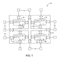
本発明に従う例示的プログラマブルロジックデバイス10は、図1に示される。プログラマブルロジックデバイス10は、デバイス10のドライビング信号をオフにするための、および、入出力ピン14を介して、その他のデバイスから信号を受けとるための入出力回路網12を有する。全体および局所的な垂直および水平の導線およびバスなどの相互接続リソース16は、デバイス10上の信号を伝送するために使用される。相互接続リソース16は、固定相互接続(導線)およびプログラマブル相互接続(すなわち、それぞれの固定相互接続間のプログラマブル接続)を含む。プログラマブルロジック18は、組み合わせおよび順序ロジック回路網を含み得る。プログラマブルロジック18は、カスタムロジック機能を実行するために構成され得る。相互接続リソース16に関係したプログラマブル相互接続は、プログラマブルロジック18の一部として考えられ得る。
An exemplary
プログラマブルロジックデバイス10は、ピン14および入出力回路網12を使用して、構成データ(プログラミングデータとも呼ばれる)がロードされ得るランダムアクセスメモリセルなどのプログラマブルエレメント20を含む。一旦ロードされると、プログラマブルエレメントの各々は、プログラマブルロジック18における関係するロジックコンポーネントの状態を制御する対応する静的制御出力信号を供給する。プログラマブル出力信号は、金属酸化物半導体(MOS)トランジスタのゲートを制御するために使用される。これらのトランジスタのほとんどは、一般に、プログラマブルコンポ−ネントにおけるnチャネル金属酸化物半導体(NMOS)パストランジスタであり、そのプログラマブルコンポーネントは、マルチプレクサ、ルックアップテーブル、ロジックアレイ、AND、OR、NAND、およびNORロジックゲートなどである。プログラマブルエレメント出力がハイのとき、そのプログラマブルエレメントによって制御されるパストランジスタは、オンにされ、ロジック信号を入力から出力へ伝える。プログラマブルエレメント出力がローのとき、パストランジスタはオフにされ、ロジック信号を伝えない。
プログラマブルエレメントは、任意の適切なソースからロードされ得る。典型的な配置において、プログラマブルエレメントは、ピン14および入出力回路網12を介して、外部消去可能プログラマブル読み出し専用メモリおよび構成デバイスと呼ばれる制御チップからロードされる。
The programmable element can be loaded from any suitable source. In a typical arrangement, programmable elements are loaded from a control chip called an externally erasable programmable read-only memory and configuration device via
デバイス10の回路網は、任意の適切なアーキテクチャを使用して組織化され得る。一例として、プログラマブルロジックデバイス10は、より大きなロジック領域の一連の行と列において組織され、そのロジック領域の各々は、複数のより小さいロジック領域を含む。デバイス10のロジックリソースは、関係する垂直および水平の導体などの相互接続リソース16によって相互接続され得る。これらの導体は以下のものを含み得る。デバイス10の実質的にすべてに及ぶ全体の導線、デバイス10の部分に及ぶ2分の1線または4分の1線などの部分線、特定の長さ(たとえば、いくつかのロジック領域を相互接続するに十分な)のスタッガード線、より小さい局所の線、または、任意のその他の適切な相互接続リソース配置。所望の場合は、デバイス10のロジックは、ロジックのさらに大きな部分を形成するために複数の大きな領域が相互接続される、より多くのレベルまたは層において配置され得る。さらにその他のデバイス配置は、行と列に配列されないロジックを使用し得る。
The circuitry of
デバイス10上のトランジスタは、4つの端子、すなわち、ソース、ドレイン、ゲート、およびボディを有する。ウェル端子またはバルク端子とも時々呼ばれるボディ端子は、消費電力を減らすためにバイアスされ得る。pチャネル金属酸化物半導体トランジスタにおいて、端子電圧は、プラス電源電圧(時々、Vccと呼ばれる)に対してわずかに上昇され得る。nチャネル金属酸化物半導体トランジスタにおいて、ボディ端子電圧は、接地に対していくらか下降され得る(時々、Vssと呼ばれる)。たとえば、Vssが0ボルトの場合、nチャネル金属酸化物半導体トランジスタのボディ端子は、約0〜500mVまたは0〜1000mV(たとえば、100mV、200mV、300mV、など)の範囲における大きさを有するマイナス電圧でバイアスされ得る。
The transistor on
例示的nチャネル金属酸化物半導体トランジスタ22の該略図は、図2に示される。トランジスタ22のソースは、Sのラベル付けされ、ドレインはDのラベル付けされ、ゲートはGのラベル付けされ、およびボディは、Bのラベル付けされる。図2に示されるように、ボディバイス電圧Vbiasはボディ端子Bに印加される。図2のnチャネルトランジスタ22の断面図は、図3に示される。ソースSおよびドレインDは、インプラント領域24を使用して、形成される。ゲート構造26は、酸化ケイ素などの絶縁体の薄い層およびシリサイド化ポリシリコンなどのゲート導体から形成される。ボディ端子Bは、p型ボディ領域30とのオーム接触を形成するために、インプラント領域28を使用する。
A schematic diagram of an exemplary n-channel metal
本発明の調整可能なボディバイアス回路網は、数10または数100ミリボルト(またはそれ以上)の大きさを有する安定した正確なマイナスバイアス電圧を生成し得る。これらのマイナスバイアス電圧は、消費電力を減らすために、図2および図3のトランジスタ22などのnチャネルトランジスタをバイアスするために使用される。一般に、任意の適切な数のトランジスタは、ボディバイアスが提供され得る。たとえば、デバイス10上のnチャネルトランジスタのいくつかまたはすべては、ボディバイアスが提供され得、pチャネルトランジスタのいくつかまたはすべては、ボディバイアスが提供され得る。広範囲にボディバイアスを提供することの利点は、デバイス10の消費電力が最小限にされ得ることである。ボディバイアスを選択的に使用することの利点は、性能が最適化されることである。たとえば、ボディバイアスは、最大限の性能が所望されるクリティカル信号パスにおいて、回避(または減少)され得る。
The adjustable body bias network of the present invention can generate a stable and accurate negative bias voltage having a magnitude of tens or hundreds of millivolts (or more). These negative bias voltages are used to bias n-channel transistors such as
デバイス10上のどの回路がボディバイアスを備えられるべきこと、および使用すべきバイアス量に関する決定は、設計工程時にロジック設計者またはCADツールによって行われ得る。これらの決定に基づき、CADツールは、調整可能なボディバイアス回路網を調整するための構成データを生成し得る。一旦プログラマブルロジックデバイスにロードされると、構成データは、バイアスをデバイス10の種々の部分のために選択的にオンおよびオフするために、およびデバイス10の種々の部分のために使用されるバイアス量を調整するために(たとえば、デバイス10のある部分における性能を最大限にし、デバイス10のその他の部分における消費電力の節約を最大限にするために)、使用され得る。一般に、任意の適切な数の異なるボディバイアス電圧は、所定のプログラマブルロジックデバイスにおいて生成され得る。nチャネル金属酸化物半導体トランジスタのための単一のボディバイアス電圧の生成が、一例として記述される。
Decisions regarding which circuits on
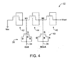
マイナスボディバイアス電圧Vbiasは、nチャネル金属酸化物半導体トランジスタをバイアスするために使用される。典型的な筋書において、デバイス10の接地電圧Vssは、0ボルトである。図4に示されるタイプのチャージポンプ32は、Vssに対してマイナス(すなわち、0ボルトより低い電圧)である電圧Voutを生成するために、使用され得る。図4の例において示されるチャージポンプ32は、二段ポンプである。これは単に例示である。チャージポンプ32は、任意の数の段(たとえば、三段またはそれ以上の段)を有し得る。
The negative body bias voltage Vbias is used to bias the n-channel metal oxide semiconductor transistor. In a typical scenario, the ground voltage Vss of
図4に示されるように、クロック信号CLKおよびその逆のNCLKは、端子34および36にそれぞれ印加される。コンデンサ38および40は、MOSトランジスタ構造から形成される金属酸化物半導体トランジスタコンデンサ(MOSコンデンサと時々呼ばれる)である。コンデンサ38および40におけるコンデンサ誘電体は、MOSトランジスタ構造におけるゲート絶縁体から形成される。各コンデンサの一つの電極は、トランジスタゲート端子から形成される。各コンデンサのもう一方の電極は、ドレイン、ソース、およびボディ端子から形成され、図4に示されるように、それらは電気的に接続される。チャージポンプ32においてMOSコンデンサを使用することは、有利である。理由は、MOSコンデンサは、デバイス10上で直ちに使用可能であり、半導体製造工程時に特別な工程段階を必要としないからである。
As shown in FIG. 4, the clock signal CLK and its inverse NCLK are applied to
チャージポンプ32は、ダイオード42、44、および46を形成するために接続される端子を有する3つのトランジスタを有する。その他のダイオード構造は、所望に応じ、ダイオード42、44、および46を形成するために使用され得る。ダイオード42、44、および46がダイオード記号を使用して表され、MOSトランジスタコンデンサ38および40がコンデンサ記号を使用して表される、図4のチャージポンプ32の回路図は、図5に示される。
チャージポンプ32の動作は、図6のタイミング線図において示される。クロック信号CLKおよびNCLKは、図6の第1および第2トレースにおいて示される。ノードN1およびN2における電圧は、図6の第3および第4トレースにおいて示される。図6の第5トレースは、チャージポンプ出力における電圧Voutを示す。
The operation of the
最初に、時間t1において、チャージポンプ32のノードN1における電圧は、図6の第3トレースによって示されるように、0ボルトである。時間t2において、クロック信号CLKは上昇し、その逆のNCLKは降下する。時間t2おける信号CLKの上昇時に、コンデンサ38全体の電圧は変化しない。その結果、ノードN1における電圧は、時間t2において上昇する。ノードN1における電圧の上昇は、ダイオード42をオンにする。ノードN1における電圧の最大上昇は、ダイオード42のオンとなった電圧でキャップされ(約0.6ボルトかまたは一つのトランジスタ閾電圧Vt)、それはCLKの大きさより少ない。
Initially, at time t1, the voltage at node N1 of
時間t3において、信号CLKは降下し、信号NCLKは上昇する。コンデンサ38全体の電圧は、時間t3における信号遷移時に変化しないので、図6の第3トレースに示されるように、信号CLKにおける降下はノードN1における電圧の降下の原因となる。ノードN2における電圧は、ダイオード44がオンになっているので、ノードN1における電圧より1ダイオードオン電圧(約0.6ボルトまたは1トランジスタ閾電圧Vt)高い。
At time t3, signal CLK falls and signal NCLK rises. Since the voltage across
時間t4において、信号CLKは上昇し、信号NCLKは降下する。コンデンサ40の全体の電圧は、時間t4おける遷移時に変化しないので、ノードN2における電圧は、時間t4において降下し、端子36のNCLK信号における降下に続く。このことは図6の第5のトレースに示されるように、チャージポンプ32の出力端子における電圧Voutを低くする。電圧Voutは、ダイオード46がオンになっているので、N2における電圧より1ダイオードオン電圧高い。
At time t4, signal CLK rises and signal NCLK falls. Since the overall voltage of
この議論が示すように、図4および図5のチャージポンプ32は、その出力においてマイナス電圧Voutを生成する。
As this discussion shows, the
チャージポンプにおける段の数およびクロック信号のサイズは、マイナス電圧Voutのサイズに影響する。さらに、クロック信号CLKおよびNCLKは、出力電圧Voutを調整するために、選択的に可能および不能にされ得る。しかしながら、バイアス電圧Vbiasを生成するためにチャージポンプのみを使用(すなわち、VoutをVbiasとして使用)することは、チャージポンプMOSコンデンサ38および40の電圧依存特性のために、一般に好適ではない。
The number of stages in the charge pump and the size of the clock signal affect the size of the negative voltage Vout. Furthermore, the clock signals CLK and NCLK can be selectively enabled and disabled to adjust the output voltage Vout. However, using only the charge pump to generate the bias voltage Vbias (ie, using Vout as Vbias) is generally not preferred due to the voltage dependent characteristics of the charge
MOSコンデンサ38、40のようなMOSコンデンサは、典型的には、図7に示されるタイプの電圧依存性を有するキャパシタンスCを示す。Vstより大きいまたは−Vstより小さい電圧で、キャパシタンスCは、比較的一定である。この形態において、チャージポンプは予測可能に挙動し、適切な調整によって、安定して、正確な出力電圧Voutを生成することが可能である。−VstとVstとの間のコンデンサ電圧においてキャパシタンスCは、印加された電圧の関数として大幅に変化する。この形態において、チャージポンプ32の動作は、不安定である傾向がある。従って、コンデンサ38および40全体の電圧が−VstとVstとの間の条件の下でチャージポンプ32を動作することを避けることが望ましい。
MOS capacitors, such as
所定のプログラマブルロジックデバイスにおいて、Vstの値は、形成されるMOS構造のタイプに依存する。一般に、Vstの値は、一つか二つのトランジスタ閾電圧Vtにほぼ等しい(すなわち、Vstは、約0.6ボルトのVt値を有する集積回路において約1ボルトである)。Vbiasに必要な電圧レベルは、約0ボルトと−1ボルトとの間にある傾向があり、一方、図4および図5のチャージポンプは、この電圧範囲において安定した電圧を生成することにあまり適していない。その結果、電圧Vbiasを直接に生成するために、図4および図5のチャージポンプを使用することは、一般に望ましくない。 In a given programmable logic device, the value of Vst depends on the type of MOS structure being formed. In general, the value of Vst is approximately equal to one or two transistor threshold voltages Vt (ie, Vst is about 1 volt in an integrated circuit having a Vt value of about 0.6 volts). The voltage level required for Vbias tends to be between about 0 and -1 volts, while the charge pumps of FIGS. 4 and 5 are less suitable for generating a stable voltage in this voltage range. Not. As a result, it is generally undesirable to use the charge pumps of FIGS. 4 and 5 to directly generate the voltage Vbias.
本発明に従う図4および図5に示されるタイプのチャージポンプは、分圧器および
フィードバック回路網が提供され、これにより、デバイス10のnチャネル金属酸化物半導体トランジスタをバイアスするための安定した正確な電圧Vbiasを生成することが可能となる。チャージポンプは、約−1V(例として)の安定した電圧Vout(Vnegと呼ばれる)を生成する。分圧器は、数10または数100mVのVbias値を生成するために、Vnegのサイズを減少させる。これらのVbias値は、トランジスタ性能を不利益に影響することなく消費電力を減らすために、nチャネルトランジスタをバイアスするに典型的に必要とされる範囲内に入る。
A charge pump of the type shown in FIGS. 4 and 5 in accordance with the present invention is provided with a voltage divider and feedback network, thereby providing a stable and accurate voltage for biasing the n-channel metal oxide semiconductor transistor of
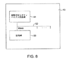
本発明に従う調整可能なボディバイアス回路配置は、図8に示される。図8に示されるように、プログラマブルロジックデバイス集積回路10は、オンチップの調整可能なボディバイアス回路網48を含む。ボディバイアス回路網48は、その出力において調整可能なボディバイアス出力電圧Vbiasを生成する。パス52などの導体パス52は、Vbiasを適切なnチャネルトランジスタのボディ端子に分配するために使用される(図8において回路網50として概略的に示される)。プログラマブルロジックデバイス10における任意の適切な数の調整可能なボディバイスジェネレータがあり得、それらの各々は、Vbiasの異なる対応する値を生成し得る。
An adjustable body bias circuit arrangement according to the present invention is shown in FIG. As shown in FIG. 8, programmable logic device integrated
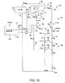
調整可能なボディバイス回路網48は、図9に示されるタイプのチャージポンプベースの回路を使用してインプリメントされ得る。図9の例において、調整可能なボディバイアス回路網48は、チャージポンプ回路56、バンドキャップ基準回路54、および調整可能電圧レギュレータ60を有する。回路網48は、その出力66において、調整可能なマイナス出力電圧Vbiasを生成する。出力66において生成される電圧Vbiasは、パス52などのパスを介して、nチャネル金属酸化物半導体トランジスタのボディ端子に印加される(図8)。
The adjustable
バンドギャップ基準回路54は基準信号を生成し、その信号はパス62を介して調整可能なレギュレータ60に供給され、パス63を介してチャージポンプ回路56に供給される。調整可能なレギュレータ60およびチャージポンプ回路56は、安定した出力信号を生成するときに基準信号を使用する。
The
チャージポンプ回路56は、マイナスチャージポンプ出力電圧Vnegを生成し、その電圧は、パス58を介して調整可能なレギュレータ60に供給される。Vnegの大きさは、好適には、Vbiasに所望される最大の大きさより大きい。たとえば、必要とされるVbiasの最強値(strongest value)は、−0.9ボルトであり、Vnegは、好適には、約−0.9ボルト以下(たとえば、−1.0ボルト、−1.2ボルト、など)である。
The
調整可能な電圧レギュレータ60は、制御信号によって制御される(制御入力64において受信される制御信号CONTROLとして図9に概略的に示される)。制御信号は、出力66において生成されるバイアス電圧Vbiasの大きさを決定するために使用される。制御信号は、バイアス電圧Vbiasを、たとえば、−100mV、−200mV、またはその他の任意の適切なバイアスレベルに設定するために使用され得る。
The
調整可能な電圧レギュレータ60およびチャージポンプ回路56は、任意の適切な回路網を使用してインプリメントされ得る。一つの適切な配置は、図10に示される。図10の例示的配置において、バンドギャップ基準回路54は、プラス電源電圧Vccpdおよび接地電圧Vssによって電力供給される。電源電圧Vccpdは、たとえば、約2.5ボルトであり得る。電源電圧Vccpdは、プログラマブルロジックデバイス10の複雑性を不必要に増加させることを避けるために、先在する電源線から好適に得られる。電源電圧Vccpdは、例として、図1の入出力回路12におけるドライバ回路網に電力供給するために使用される電源電圧と同じであり得る。
バンドギャップ基準回路54は、基準電圧Vref1およびVref2を対応する出力線70および72に供給する。Vref1およびVref2のために選ばれた特定の値は、クリティカルではない。適切なVref1値の例は、0.5ボルトである。適切なVref2値の例は、1ボルトである(Vref1の2倍)。バンドギャップ基準回路54もまた、基準電流Irefを供給する。Irefは、たとえば、10μAであり得る。
The band
チャージポンプ回路56は、チャージポンプ32、分圧器74、比較器76、および発振器78を含む。発振器78は、パス80を介してポンプ32をチャージするために、クロック信号CLKおよびNCLKを供給する。線82上の比較器76によって生成される出力は、発振器78を制御する。チャージポンプ32の出力は、電圧Vnegであり、パス90を介して電圧レギュレータ60に供給される。電圧Vnegもまた、フィードバックパス88を介して分圧器74にフィードバックされる。分圧器74は、線84上に出力信号を生成するために、VnegおよびVref2(入力73において受信される)を使用し、その出力信号は、線88を介してフィードバックされた電圧Vref1に比例する。基準電圧Vref1はパス86を介して比較器76に供給される。
The
比較器76は、線84および86上の信号を比較し、対応する出力をパス82に生成する。線84上の信号が線86上の信号より大きいとき、線82上の比較器76の出力はハイである。このことは、発振器78をオンにし、チャージポンプ32がVnegを低下させる原因となる。線84上の信号が線86上の信号より小さいとき、線82上の比較器76の出力はローである。このことは、発振器78をオフにし、Vnegは所望の値に到達したことを合図する。このフィードバック配置を使用して、Vnegの値は、その所望の値(たとえば、−1ボルト)で一定に保持される。
Comparator 76 compares the signals on
電圧Vnegは、パス90を介して、調整可能なレギュレータ60に供給され、パス
のマイナス電源を形成する。電圧Vref2は、調整可能な電圧レギュレータ60のためのプラスの電源として働く。調整可能な電圧レギュレータ60は、多数の直列接続の抵抗器98から形成される調整可能な分圧器を有する。典型的な抵抗値は、約10kO〜50kOである。電圧レギュレータ60における抵抗器連鎖の一端は、電圧Vbiasに維持される。抵抗器チェーンのもう一方の端は、プラス電源Vref2に接続される。
The voltage Vneg is supplied to the
電圧Vtapは、分圧器における抵抗器チェーンからタップオフされる。レギュレータ60は、電圧Vtapを演算増幅器94の入力の一つに供給するフィードバックパス92を有する。電圧Vtapの大きさは、調整可能な分圧器の状態によって決定される。電圧Vtapが直列接続された抵抗器98からタップされるポイントを調整することによって、分圧器ための電圧設定ポイントは調整され得る。
The voltage Vtap is tapped off from the resistor chain in the voltage divider. The
図10の例示的配置において、分圧器の直列接続された抵抗器における電圧タップポイント位置は、プログラマブルエレメント20の状態を設定することによって確立される。各プログラマブルエレメント20は対応するトランジスタ102を制御する。各プログラマブルエレメントはエレメントの内容によって決定される。デバイスプログラミング時、構成データは、プログラマブルエレメント20にロードされる。ロジック0がロードされたプログラマブルエレメントは低い出力信号を生成し、その信号に関係したトランジスタ102をオフにする。プログラマブルエレメントの一つはロジック1がロードされる。プログラマブルエレメントにおけるロジック1はそのプログラマブルエレメントの出力をハイにする。ハイ出力信号は、対応するトランジスタ102をオンにする。トランジスタ102がオンにされた位置は、分圧器68のための設定ポイントを決定する。
In the exemplary arrangement of FIG. 10, the voltage tap point position in the series connected resistor of the voltage divider is established by setting the state of the
分圧器68からの電圧Vtapは、フィードバックパス92を介して演算増幅器にフィードバックされる。演算増幅器94は適切な電源電圧(たとえば、図10の例における電圧VccpdおよびVneg)を使用して、電力供給される。演算増幅器94は、バンドギャップ基準回路54から、電流基準Irefおよび電圧基準Vref1などの基準信号を好適に受信する。電流基準Irefは入力線96を介して演算増幅器94に供給される。電圧基準信号Vref1は演算増幅器94の入力端子に印加される。
The voltage Vtap from the voltage divider 68 is fed back to the operational amplifier via the
演算増幅器94は、分圧器68からのタップされた電圧Vtapを基準電圧Vref1と比較し、対応する出力制御信号Vxを生成する。信号Vxはトランジスタ104のゲートGに印加される。トランジスタ104は通常オンであり、飽和状態において動作する。電流は、Vref2ノード69から(1Vで)Vnegノード91へ(−1Vで)、分圧器68の抵抗器およびトランジスタ104のソースおよびドレインを介して流れる。Vxが上昇すると、トランジスタ104がそのソースとドレインとの間で伝導する電流の量もまた上昇する。このことは、出力端子66における電圧Vbiasにおける降下の原因となる。Vxが降下すると、トランジスタ104を通過する電流の量は低下し、Vbiasを上昇させる。
The
演算増幅器94を介した分圧器68からのフィードバックループは、電圧Vbiasをその電圧の所望のレベルで正確に維持する。Vbiasがその電圧の設定ポイントよりわずか上に上昇し始める場合(たとえば、−100mVから−99mVに上昇することによって)、Vtapはわずかに上昇する(たとえば、500mVから501mVへ)。パス92によって供給されるフィードバックは演算増幅器94の出力を増加させるので、演算増幅器94の出力における電圧Vxは上昇する。Vxの上昇した値に応答し、トランジスタ104を介した電流は増加する。トランジスタ104を介した電流を増加させることは、Vbiasをその電圧の所望の設定ポイント値(この例では−100mV)に向けて降下させ(たとえば、−99mVから−100mVへ)戻す。Vbiasがその電圧の設定ポイントよりわずか下に降下し始める場合、パス92を介したフィードバックは、Vbiasを上昇させる(たとえば、−101mVから−100mVへ)。
A feedback loop from voltage divider 68 through
分圧器68において使用される抵抗器98の数は、調整可能な電圧レギュレータ60のための電圧ステップの所望の数によって決定される。多数の抵抗器98が使用される場合、比較的多数の電圧ステップがあり、電圧レギュレータ60は、所望のVbiasレベルを正確度の高いレベルで生成し得る。より少ない抵抗器98が使用される場合、各電圧ステップはより大きくなり、より低い正確度が使用可能であるが、回路の複雑性は減少される。一般に、抵抗器98および関係するタップトランジスタ102の任意の適切な数が、分圧器68において使用され得る。
The number of
図10の演算増幅器94のために使用し得る例示的回路網は、図11に示される。図11に示されるように、演算増幅器94はプラス電源電圧Vccpdおよびマイナス電圧供給Vnegを使用して電力供給される。演算増幅器94の出力126は、トランジスタ104のゲートに印加される電圧Vxを生成する(図10)。
An exemplary network that may be used for the
基準電流Irefは、線96から入力106に印加される。トランジスタ108および109は、電流ミラーを形成するので、大きさIrefの電流はパス110を介して流れる。トランジスタ112および114もまた、電流ミラーを形成するので、電流Irefはパス116を介して流れる。図11の電流ミラーは、それらのトランジスタが等しい強さを有するので、ミラー比1を有する。所望に応じ、他のミラー比を有する電流ミラーが使用され得る。
Reference current Iref is applied to input 106 from
マイナス入力128およびプラス入力130は、それぞれ、電圧Vrefおよび電圧Vtapを受信する。基準Vref1は、バンドギャップ基準回路54によって生成され(図10)、一定である。Vbiasはその所望の設定ポイント値あたりでわずかに変動するので、Vtapの値は、Vref1よりわずかに上および下に変動する。基準値Vref1に対するVtapの値は、電流がパス118かまたはパス132を介して進むかどうかを決定する。
The
VtapがVref1より大きいとき、pチャネル金属酸化物半導体トランジスタ134は、pチャネル金属酸化物半導体トランジスタ136より強くオンにされる。このことは、パス116における電流Irefをパス132よりパス118の方に比較的多く進ませる。トランジスタ120および122は電流ミラーを形成するので、パス118に進んだ追加の電流は、追加の電流をパス124に進ませるようにする。
When Vtap is greater than Vref1, the p-channel metal
VtapがVref1より小さいとき、電流はパス132に進められる。トタンジスタ138および140は電流ミラーを形成するので、パス132に進められた追加の電流は、より多くの電流をパス142に進ませるようにする。安定した状態において、Vtapの値は、Vref1に落ち着き、電流の等しい量は演算増幅器94の左手および右手の支線を介して流れる。
When Vtap is less than Vref1, the current is advanced to
トランジスタ146および144は、それぞれ、パス124および142を介して流れる電流をノ−ド150および148における電圧に変換するロードトランジスタである。パス142を介する電流が端子130におけるVtapの減少のため増加するとき、電圧Vxは降下する。パス142を介する電流が、端子130におけるVtapの値の増加のために減少するとき、電圧Vxは上昇する。
図10の例において、分圧器回路68の設定は、プログラマブルエレメント20へロードされる構成データを使用して調整される。この種の状況において、プログラマブルエレメント20は、調整可能なレギュレータ60ための制御信号として働く(図9のパス64の制御(CONTROL)信号として示される)。このタイプの配置は、単に例示的である。分圧器68および電圧レギュレータ60を制御するための任意の適切な技術は、所望に応じ使用され得る。たとえば、制御信号を電圧タップトランジスタ102に供給するために、その他の技術が使用され得る。
In the example of FIG. 10, the settings of voltage divider circuit 68 are adjusted using configuration data loaded into
トランジスタ102を制御するための例示的配置は、図12、13、14、および15に示される。
Exemplary arrangements for controlling
図12の配置において、単一のプログラマブルエレメント20は各トランジスタ102と関係している。プログラマブルエレメント20の出力は、それぞれの制御線152を使用してトランジスタ102のゲートに供給される。
In the arrangement of FIG. 12, a single
図13は、デコーダ156を使用する制御配置を示す。プログラマブルエレメント20は、制御信号を入力線158上のデコーダ156に供給されるために使用される。デコーダ156は、入力線158上のデコードされない制御信号を線160上の対応するデコードされる制御信号へ変換するロジックを含む。線160はこれらの制御信号をそれぞれのトランジスタ102のゲートへ伝送するために使用される。
FIG. 13 shows a control arrangement using the
図13のデコータ156などのデコーダの使用は、デバイス10の複雑性を増加させる。さらに、回路物体は、デコーダ156のロジックおよび伝送線158および160を必要とする。それにもかかわらず、デコーダ156などのデコーダの使用は、プログラマブルエレメント20の必要性を減らす。たとえば、Nプログラマブルエレメントを使用して2N線160を制御することは可能である。比較的に多数のトランジスタ102がある状況において、各トランジスタ102を制御するために、デコーダ156を使用することは、別のプログラマブルエレメント使用することより効率的である。
The use of a decoder such as the
所望に応じ、外部制御信号は、トランジスタ102のゲートを制御するために使用される。図14に示されるように、各トランジスタ102は、関係するパス162を介して、対応する入出力ピン14から制御信号を受信し得る。図15の配置において、デコーダ166は、入出力ピンとトランジスタ102との間に置かれる。パス164は、デコードされない制御信号を入出力ピン14からデコーダ166に伝える。パス168は、デコードされた制御信号をトランジスタ102に伝える。
An external control signal is used to control the gate of
図14の線162および図15の線164のための制御信号は、内部ソースから供給され得る(たとえば、図1のプログラマブルロジック18におけるロジックまたはデバイス10のハードワイヤーのロジック)。これらの制御信号は、デバイス10の動作時に動的に生成され得る。
Control signals for
これらのアプローチの組み合わせもまた、使用され得る。たとえば、トランジスタ102のいくつかは、図12に示されるように専用のプログラマブルエレメント20からの信号によって、および/または内部供給の信号、および/または図14の線162上の外部供給の信号によって制御され得、一方その他のトランジスタ102はデコーダを使用して制御され得る。デコーダは、デコードされない制御信号がプログラマブルエレメント20、プログラマブルロジック18、または外部ソースから供給され得る。
A combination of these approaches can also be used. For example, some of the
上記は、本発明の原理の単なる例示であり、本発明の範囲と精神から逸脱することなく、当業者によって、種々の改変がなされ得る。 The foregoing is merely illustrative of the principles of this invention and various modifications can be made by those skilled in the art without departing from the scope and spirit of the invention.
10 プログラマブルロジックデバイス
12 入出力回路網
14 入出力ピン
16 相互接続リソース
18 プログラマブルロジック
20 プログラマブルエレメント
22 トランジスタ
24、28 インプラント領域
26 ゲート構造
30 p型ボディ領域
32 チャージポンプ
34、36 端子
38、40 コンデンサ
42、44、46 ダイオード
48 ボディバイアス回路網
50 回路網
52、58 パス
54 バンドギャプ基準回路
56 チャージポンプ回路
60 電圧レギュレータ
DESCRIPTION OF
Claims (16)
ボディ端子を有するnチャネル金属酸化物半導体トランジスタと、
負のボディバイアス電圧を該ボディ端子へ印加する調整可能なチャージポンプベースのボディバイアス回路網であって、該集積回路は、プログラマブルロジックデバイス集積回路を備え、該調整可能なチャージポンプベースのボディバイアス回路網は、調整可能な電圧レギュレータを備えている、調整可能なチャージポンプベースのボディバイアス回路網と
を備え、該集積回路は、構成データがロードされる複数のプログラマブルエレメントをさらに備え、該複数のプログラマブルエレメントのうちのいくつかは、該調整可能な電圧レギュレータを制御する出力信号を生成する、集積回路。 An integrated circuit,
An n-channel metal oxide semiconductor transistor having a body terminal;
An adjustable charge pump based body bias network for applying a negative body bias voltage to the body terminal, the integrated circuit comprising a programmable logic device integrated circuit, the adjustable charge pump based body bias The network comprises an adjustable charge pump based body bias circuitry comprising an adjustable voltage regulator, the integrated circuit further comprising a plurality of programmable elements loaded with configuration data, An integrated circuit in which some of the programmable elements generate an output signal that controls the adjustable voltage regulator.
ボディ端子を有するnチャネル金属酸化物半導体トランジスタと、
負のボディバイアス電圧を該ボディ端子へ印加する調整可能なチャージポンプベースのボディバイアス回路網であって、該集積回路は、プログラマブルロジックデバイス集積回路を備え、該調整可能なチャージポンプベースのボディバイアス回路網は、調整可能な電圧レギュレータを備えている、調整可能なチャージポンプベースのボディバイアス回路網と
を備え、該集積回路は、構成データがロードされる複数のプログラマブルエレメントであって、該複数のプログラマブルエレメントのうちのいくつかは、デコードされない制御信号を生成する、複数のプログラマブルエレメントと、
該デコードされない制御信号を受信し、対応するデコードされる制御信号を該調整可能な電圧レギュレータに印加するデコーダと
をさらに備える、集積回路。 An integrated circuit,
An n-channel metal oxide semiconductor transistor having a body terminal;
An adjustable charge pump based body bias network for applying a negative body bias voltage to the body terminal, the integrated circuit comprising a programmable logic device integrated circuit, the adjustable charge pump based body bias The network comprises an adjustable charge pump based body biasing network with an adjustable voltage regulator, the integrated circuit comprising a plurality of programmable elements loaded with configuration data, A plurality of programmable elements that generate a non-decoded control signal;
An integrated circuit further comprising: a decoder that receives the undecoded control signal and applies the corresponding decoded control signal to the adjustable voltage regulator.
ボディ端子を有するnチャネル金属酸化物半導体トランジスタと、
負のボディバイアス電圧を該ボディ端子へ印加する調整可能なチャージポンプベースのボディバイアス回路網と
を備え、
該調整可能なチャージポンプベースのボディバイアス回路網は、
負のチャージポンプ出力電圧を生成するチャージポンプ回路と、
複数のプログラマブルエレメントであって、該複数のプログラマブルエレメントのうちの少なくともいくつかが、構成データがロードされ、出力信号を生成するプログラマブルエレメントである、複数のプログラマブルエレメントと、
該出力信号に基づいて、該負のチャージポンプ出力電圧を用いて、該負のボディバイアス電圧を生成する調整可能な電圧レギュレータと
を備える、集積回路。 An integrated circuit,
An n-channel metal oxide semiconductor transistor having a body terminal;
An adjustable charge pump based body bias network for applying a negative body bias voltage to the body terminal;
The adjustable charge pump based body bias network is:
A charge pump circuit for generating a negative charge pump output voltage;
A plurality of programmable elements, at least some of the programmable elements of said plurality of configuration data is loaded, a programmable element for generating an output signal, and a plurality of programmable elements,
An adjustable voltage regulator that uses the negative charge pump output voltage to generate the negative body bias voltage based on the output signal.
負の電圧を生成するチャージポンプと、
複数のプログラマブルエレメントであって、該複数のプログラマブルエレメントのうちの少なくともいくつかが、構成データがロードされ、出力信号を生成するプログラマブルエレメントである、複数のプログラマブルエレメントと、
該出力信号に基づいて、該チャージポンプからの該負の電圧を用いて、負のトランジスタボディバイアス電圧を生成する調整可能な電圧レギュレータと
を備える、トランジスタボディバイアス回路。 A transistor body bias circuit on an integrated circuit,
A charge pump that generates a negative voltage;
A plurality of programmable elements, at least some of the programmable elements of said plurality of configuration data is loaded, a programmable element for generating an output signal, and a plurality of programmable elements,
A transistor body bias circuit comprising: an adjustable voltage regulator that generates a negative transistor body bias voltage using the negative voltage from the charge pump based on the output signal.
負のボディバイアス電圧が印加されるボディ端子を有するnチャネル金属酸化物半導体トランジスタを含むプログラマブルロジックと、
基準電圧を供給するバンドギャップ基準回路と、
端子を有する調整可能な電圧レギュレータであって、該端子は、負のチャージポンプ出力電圧を受信し、該バンドギャップ基準回路から該基準電圧を受信し、該負のボディバイアス電圧を該プログラマブルロジックにおける該nチャネル金属酸化物半導体トランジスタの該ボディ端子に供給する、調整可能な電圧レギュレータと、
構成データがロードされる複数のプログラマブルエレメントであって、該複数のプログラマブルエレメントのうちのいくつかが、該調整可能な電圧レギュレータを制御する出力信号を生成する、複数のプログラマブルエレメントと
を備える、プログラマブルロジックデバイス集積回路。 A programmable logic device integrated circuit comprising:
Programmable logic including an n-channel metal oxide semiconductor transistor having a body terminal to which a negative body bias voltage is applied;
A bandgap reference circuit for supplying a reference voltage;
An adjustable voltage regulator having a terminal that receives a negative charge pump output voltage, receives the reference voltage from the bandgap reference circuit, and transmits the negative body bias voltage in the programmable logic. An adjustable voltage regulator for supplying to the body terminal of the n-channel metal oxide semiconductor transistor;
A plurality of programmable elements loaded with configuration data, wherein some of the plurality of programmable elements comprises a plurality of programmable elements that generate an output signal that controls the adjustable voltage regulator Logic device integrated circuit.
該調整可能な分圧器によって受信される前記負のチャージポンプ出力電圧を生成するチャージポンプ回路をさらに備える、請求項7に記載のプログラマブルロジックデバイス集積回路。 The adjustable voltage regulator comprises an adjustable voltage divider, and the programmable logic device comprises:
The programmable logic device integrated circuit of claim 7, further comprising a charge pump circuit that generates the negative charge pump output voltage received by the adjustable voltage divider.
前記基準電圧を受信し、出力信号を供給する演算増幅器と、
該演算増幅器から該出力信号を受信するゲートを有するトランジスタと、
該トランジスタに接続された抵抗器のチェーンと
をさらに備える、請求項7に記載のプログラマブルロジックデバイス集積回路。 The adjustable voltage regulator is:
An operational amplifier that receives the reference voltage and provides an output signal;
A transistor having a gate for receiving the output signal from the operational amplifier;
The programmable logic device integrated circuit of claim 7, further comprising: a chain of resistors connected to the transistor.
前記調整可能な分圧器において直列接続された抵抗器のチェーンと、
関係したタップ電圧を規定する選択可能な分圧器タップポイントを確立するために、該直列接続された抵抗器のそれぞれのペア間に接続される複数のトランジスタと
をさらに備える、請求項7に記載のプログラマブルロジックデバイス集積回路。 The adjustable voltage regulator is:
A chain of resistors connected in series in the adjustable voltage divider;
A plurality of transistors connected between each pair of said series connected resistors to establish a selectable voltage divider tap point defining an associated tap voltage. Programmable logic device integrated circuit.
ボディ端子を有するnチャネル金属酸化物半導体トランジスタと、
負のボディバイアス電圧を該ボディ端子へ印加する調整可能なチャージポンプベースのボディバイアス回路網と
を備え、該調整可能なチャージポンプベースのボディバイアス回路網は、
負のチャージポンプ出力電圧を生成するチャージポンプ回路と、
該負のチャージポンプ出力電圧を用いて、該負のボディバイアス電圧を生成する調整可能な電圧レギュレータであって、該調整可能な電圧レギュレータは、調整可能な分圧器を含み、該調整可能な電圧レギュレータは、複数の直列接続された抵抗器と複数のトランジスタとを含み、該トランジスタは、ゲートを有し、該直列接続された抵抗器のそれぞれのペアの間で接続され、該トランジスタは、該直列接続された抵抗器の電圧タップポイントの位置を規定するために、該トランジスタのゲートに印加される制御信号によって制御される、調整可能な電圧レギュレータと、
構成データがロードされる複数のプログラマブルエレメントであって、該トランジスタを制御する該制御信号は、該複数のプログラマブルエレメントの少なくともいくつかの出力から印加される、複数のプログラマブルエレメントと
を備えている、集積回路。 An integrated circuit,
An n-channel metal oxide semiconductor transistor having a body terminal;
An adjustable charge pump based body bias network for applying a negative body bias voltage to the body terminal, the adjustable charge pump based body bias network comprising:
A charge pump circuit for generating a negative charge pump output voltage;
An adjustable voltage regulator that uses the negative charge pump output voltage to generate the negative body bias voltage, the adjustable voltage regulator including an adjustable voltage divider, the adjustable voltage The regulator includes a plurality of series-connected resistors and a plurality of transistors, the transistors having a gate and connected between each pair of the series-connected resistors, An adjustable voltage regulator controlled by a control signal applied to the gate of the transistor to define the position of the voltage tap point of the resistor connected in series;
A plurality of programmable elements loaded with configuration data, the control signal controlling the transistors comprising a plurality of programmable elements applied from at least some outputs of the plurality of programmable elements; Integrated circuit.
負の電圧を生成するチャージポンプと、
該チャージポンプからの該負の電圧を用いて、負のトランジスタボディバイアス電圧を生成する調整可能な電圧レギュレータと、
複数のプログラマブルエレメントであって、該複数のプログラマブルエレメントのうちの少なくともいくつかが、構成データがロードされ、対応する出力信号を生成するプログラマブルエレメントであり、該対応する出力信号は、該調整可能な電圧レギュレータを制御するために該調整可能な電圧レギュレータに印加され、これにより、該負のトランジスタボディバイアス電圧が調整される、複数のプログラマブルエレメントと
を備える、トランジスタボディバイアス回路。 A transistor body bias circuit on an integrated circuit,
A charge pump that generates a negative voltage;
An adjustable voltage regulator that uses the negative voltage from the charge pump to generate a negative transistor body bias voltage;
A plurality of programmable elements, wherein at least some of the plurality of programmable elements are programmable elements that are loaded with configuration data and generate a corresponding output signal, the corresponding output signal being adjustable A transistor body bias circuit comprising: a plurality of programmable elements applied to the adjustable voltage regulator to control the voltage regulator, thereby adjusting the negative transistor body bias voltage.
ボディ端子を有するnチャネル金属酸化物半導体トランジスタと、
調整可能なボディバイアス回路網であって、該調整可能なボディバイアス回路網は、少なくとも1つの制御信号を受信する制御入力経路を有し、該制御信号に基づいて負のボディバイアス電圧を該ボディ端子に印加する出力経路を有する、調整可能なボディバイアス回路網と、
複数のプログラマブルエレメントであって、該複数のプログラマブルエレメントのうちの少なくともいくつかが、構成データがロードされ、対応する出力信号を生成するプログラマブルエレメントであり、該対応する出力信号は、該調整可能なボディバイアス回路網を制御するために該調整可能なボディバイアス回路網に印加され、これにより、該負のボディバイアス電圧が調整される、複数のプログラマブルエレメントと
を備える、集積回路。 An integrated circuit,
An n-channel metal oxide semiconductor transistor having a body terminal;
An adjustable body bias network, the adjustable body bias network having a control input path for receiving at least one control signal, and applying a negative body bias voltage based on the control signal to the body An adjustable body bias network having an output path applied to the terminals;
A plurality of programmable elements, wherein at least some of the plurality of programmable elements are programmable elements that are loaded with configuration data and generate a corresponding output signal, the corresponding output signal being adjustable An integrated circuit comprising: a plurality of programmable elements that are applied to the adjustable body bias circuitry to control the body bias circuitry , thereby adjusting the negative body bias voltage.
Applications Claiming Priority (1)
| Application Number | Priority Date | Filing Date | Title |
|---|---|---|---|
| US11/369,664 US7495471B2 (en) | 2006-03-06 | 2006-03-06 | Adjustable transistor body bias circuitry |
Publications (3)
| Publication Number | Publication Date |
|---|---|
| JP2007243178A JP2007243178A (en) | 2007-09-20 |
| JP2007243178A5 JP2007243178A5 (en) | 2010-03-11 |
| JP4648346B2 true JP4648346B2 (en) | 2011-03-09 |
Family
ID=38110608
Family Applications (1)
| Application Number | Title | Priority Date | Filing Date |
|---|---|---|---|
| JP2007042839A Expired - Fee Related JP4648346B2 (en) | 2006-03-06 | 2007-02-22 | Adjustable transistor body bias network |
Country Status (4)
| Country | Link |
|---|---|
| US (2) | US7495471B2 (en) |
| EP (1) | EP1833152A1 (en) |
| JP (1) | JP4648346B2 (en) |
| CN (1) | CN101257300A (en) |
Families Citing this family (43)
| Publication number | Priority date | Publication date | Assignee | Title |
|---|---|---|---|---|
| JP2007251351A (en) | 2006-03-14 | 2007-09-27 | Renesas Technology Corp | Semiconductor device |
| US7642754B2 (en) * | 2006-06-08 | 2010-01-05 | Semiconductor Components Industries, L.L.C. | Method of forming a voltage regulator and structure therefor |
| KR100817058B1 (en) * | 2006-09-05 | 2008-03-27 | 삼성전자주식회사 | Body biasing control circuit using lookup table and body biasing control method thereof |
| JP2008136047A (en) * | 2006-11-29 | 2008-06-12 | Sony Corp | Solid-state imaging apparatus and imaging apparatus |
| US8183843B2 (en) * | 2007-01-26 | 2012-05-22 | Infineon Technologies Ag | Voltage regulator and associated methods |
| US8115462B2 (en) * | 2007-06-20 | 2012-02-14 | Atmel Corporation | Voltage regulator for an integrated circuit |
| US7800402B1 (en) * | 2007-11-05 | 2010-09-21 | Altera Corporation | Look-up table overdrive circuits |
| DE102008007029B4 (en) * | 2008-01-31 | 2014-07-03 | Globalfoundries Dresden Module One Limited Liability Company & Co. Kg | Operation of an electronic circuit with body-controlled dual-channel transistor and SRAM cell with body-controlled dual-channel transistor |
| KR100961210B1 (en) * | 2008-11-04 | 2010-06-09 | 주식회사 하이닉스반도체 | Control signal generation circuit and sense amplifier circuit using the same |
| US8081502B1 (en) | 2008-12-29 | 2011-12-20 | Altera Corporation | Memory elements with body bias control |
| US8742831B2 (en) * | 2009-02-23 | 2014-06-03 | Honeywell International Inc. | Method for digital programmable optimization of mixed-signal circuits |
| CN101867015A (en) * | 2009-04-16 | 2010-10-20 | 台湾积体电路制造股份有限公司 | By applying the P-substrate bias and regulating the program current that threshold voltage improves MTJ |
| CN101814829B (en) * | 2010-04-22 | 2015-09-16 | 上海华虹宏力半导体制造有限公司 | The generating circuit from reference voltage of charge pump circuit and charge pump circuit |
| KR101143470B1 (en) | 2010-07-02 | 2012-05-08 | 에스케이하이닉스 주식회사 | Voltage regulation circuit |
| US8416011B2 (en) | 2010-11-08 | 2013-04-09 | Lsi Corporation | Circuit and method for generating body bias voltage for an integrated circuit |
| CN103534950B (en) * | 2011-05-16 | 2017-07-04 | 株式会社半导体能源研究所 | Programmable logic device |
| US8416009B2 (en) | 2011-07-13 | 2013-04-09 | International Business Machines Corporation | Solutions for controlling bulk bias voltage in an extremely thin silicon-on-insulator (ETSOI) integrated circuit chip |
| US9024679B2 (en) * | 2011-07-25 | 2015-05-05 | Macronix International Co., Ltd. | Standby charge pump system |
| DE102013022449B3 (en) * | 2012-05-11 | 2019-11-07 | Semiconductor Energy Laboratory Co., Ltd. | Semiconductor device and electronic device |
| US9348959B1 (en) * | 2012-06-29 | 2016-05-24 | Xilinx, Inc. | Optimizing supply voltage and threshold voltage |
| US8847565B2 (en) * | 2012-09-14 | 2014-09-30 | Nxp B.V. | Shunt regulator for adverse voltage/circuit conditions |
| US9112495B1 (en) * | 2013-03-15 | 2015-08-18 | Mie Fujitsu Semiconductor Limited | Integrated circuit device body bias circuits and methods |
| JP6147918B2 (en) * | 2013-05-17 | 2017-06-14 | インテル コーポレイション | On-chip power generator using dynamic circuit reference |
| JP6406926B2 (en) | 2013-09-04 | 2018-10-17 | 株式会社半導体エネルギー研究所 | Semiconductor device |
| US9088280B2 (en) * | 2013-10-30 | 2015-07-21 | Freescale Semiconductor, Inc. | Body bias control circuit |
| US9577626B2 (en) | 2014-08-07 | 2017-02-21 | Skyworks Solutions, Inc. | Apparatus and methods for controlling radio frequency switches |
| KR102211167B1 (en) | 2014-08-14 | 2021-02-02 | 삼성전자주식회사 | Body bias voltage generator and system-on-chip having the same |
| US9467124B2 (en) * | 2014-09-30 | 2016-10-11 | Skyworks Solutions, Inc. | Voltage generator with charge pump and related methods and apparatus |
| US9917507B2 (en) | 2015-05-28 | 2018-03-13 | Sandisk Technologies Llc | Dynamic clock period modulation scheme for variable charge pump load currents |
| US9647536B2 (en) | 2015-07-28 | 2017-05-09 | Sandisk Technologies Llc | High voltage generation using low voltage devices |
| WO2017037568A1 (en) * | 2015-08-31 | 2017-03-09 | Semiconductor Energy Laboratory Co., Ltd. | Semiconductor device or electronic device including the semiconductor device |
| US9520776B1 (en) | 2015-09-18 | 2016-12-13 | Sandisk Technologies Llc | Selective body bias for charge pump transfer switches |
| CN106253665B (en) * | 2016-08-29 | 2019-06-25 | 深圳市华星光电技术有限公司 | Increase the charge pump of buck amplitude |
| CN108205349A (en) * | 2016-12-19 | 2018-06-26 | 北京兆易创新科技股份有限公司 | A kind of band-gap reference circuit |
| US10483985B2 (en) * | 2017-01-23 | 2019-11-19 | Samsung Electronics Co., Ltd. | Oscillator using supply regulation loop and operating method thereof |
| KR102426729B1 (en) | 2017-08-11 | 2022-07-29 | 삼성전자주식회사 | Nonvolatile memory device and operating method of nonvolatile memory device |
| CN107357351B (en) * | 2017-08-15 | 2018-10-26 | 电子科技大学 | A kind of NMOS LDO based on self-powered charge pump architecture |
| US10552563B2 (en) * | 2018-01-10 | 2020-02-04 | Qualcomm Incorporated | Digital design with bundled data asynchronous logic and body-biasing tuning |
| US10469097B1 (en) | 2018-12-06 | 2019-11-05 | Nxp Usa, Inc. | Body bias circuit for current steering DAC switches |
| US11271566B2 (en) * | 2018-12-14 | 2022-03-08 | Integrated Device Technology, Inc. | Digital logic compatible inputs in compound semiconductor circuits |
| KR102071354B1 (en) * | 2019-11-13 | 2020-01-30 | 주식회사 스카이칩스 | Buck-Boost DC-DC converter |
| KR20210084955A (en) * | 2019-12-30 | 2021-07-08 | 에스케이하이닉스 주식회사 | Memory device including data input/output circuit |
| WO2021220629A1 (en) * | 2020-04-27 | 2021-11-04 | ソニーセミコンダクタソリューションズ株式会社 | Dc/dc converter |
Citations (9)
| Publication number | Priority date | Publication date | Assignee | Title |
|---|---|---|---|---|
| JP2000066744A (en) * | 1998-08-17 | 2000-03-03 | Nec Corp | Semiconductor device with built-in regulator |
| JP2003330551A (en) * | 2002-05-09 | 2003-11-21 | Fuji Electric Co Ltd | Voltage variable regulator |
| JP2004241122A (en) * | 2004-05-06 | 2004-08-26 | Matsushita Electric Ind Co Ltd | Regulator |
| JP2004273103A (en) * | 2003-03-06 | 2004-09-30 | Samsung Electronics Co Ltd | Voltage regulator circuit and semiconductor memory device |
| JP2005503668A (en) * | 2001-09-18 | 2005-02-03 | ザイリンクス インコーポレイテッド | Structure and method for selectively applying a well bias to a portion of a programmable device |
| JP2005136322A (en) * | 2003-10-31 | 2005-05-26 | Toshiba Corp | Semiconductor integrated circuit and power-supply-voltage/substrate-bias control circuit |
| JP2005157620A (en) * | 2003-11-25 | 2005-06-16 | Matsushita Electric Ind Co Ltd | Semiconductor integrated circuit |
| JP2006510121A (en) * | 2002-12-23 | 2006-03-23 | インテル・コーポレーション | One method and apparatus for reducing power consumption through dynamic control of supply voltage and body bias |
| JP2007538474A (en) * | 2004-05-19 | 2007-12-27 | アルテラ コーポレイション | Apparatus and method for tuning integrated circuit performance |
Family Cites Families (78)
| Publication number | Priority date | Publication date | Assignee | Title |
|---|---|---|---|---|
| US5103160A (en) * | 1991-04-25 | 1992-04-07 | Hughes Aircraft Company | Shunt regulator with tunnel oxide reference |
| DE4221575C2 (en) | 1992-07-01 | 1995-02-09 | Ibm | Integrated CMOS semiconductor circuit and data processing system with integrated CMOS semiconductor circuit |
| US5341034A (en) | 1993-02-11 | 1994-08-23 | Benchmarq Microelectronics, Inc. | Backup battery power controller having channel regions of transistors being biased by power supply or battery |
| KR0169157B1 (en) | 1993-11-29 | 1999-02-01 | 기다오까 다까시 | Semiconductor circuit and mos-dram |
| US5422591A (en) | 1994-01-03 | 1995-06-06 | Sgs-Thomson Microelectronics, Inc. | Output driver circuit with body bias control for multiple power supply operation |
| US5689209A (en) | 1994-12-30 | 1997-11-18 | Siliconix Incorporated | Low-side bidirectional battery disconnect switch |
| US5670907A (en) | 1995-03-14 | 1997-09-23 | Lattice Semiconductor Corporation | VBB reference for pumped substrates |
| JP2931776B2 (en) | 1995-08-21 | 1999-08-09 | 三菱電機株式会社 | Semiconductor integrated circuit |
| US5661685A (en) | 1995-09-25 | 1997-08-26 | Xilinx, Inc. | Programmable logic device with configurable power supply |
| US5600264A (en) | 1995-10-16 | 1997-02-04 | Xilinx, Inc. | Programmable single buffered six pass transistor configuration |
| US5689144A (en) | 1996-05-15 | 1997-11-18 | Siliconix Incorporated | Four-terminal power MOSFET switch having reduced threshold voltage and on-resistance |
| KR100189752B1 (en) | 1996-06-01 | 1999-06-01 | 구본준 | Power pump circuit with independent well bias voltage |
| KR100203136B1 (en) | 1996-06-27 | 1999-06-15 | 김영환 | Voltage generator preventing latch-up |
| JP3264622B2 (en) | 1996-07-16 | 2002-03-11 | 株式会社東芝 | Semiconductor device |
| US6593799B2 (en) | 1997-06-20 | 2003-07-15 | Intel Corporation | Circuit including forward body bias from supply voltage and ground nodes |
| US6411156B1 (en) | 1997-06-20 | 2002-06-25 | Intel Corporation | Employing transistor body bias in controlling chip parameters |
| US6535034B1 (en) | 1997-07-30 | 2003-03-18 | Programmable Silicon Solutions | High performance integrated circuit devices adaptable to use lower supply voltages with smaller device geometries |
| US5841694A (en) | 1997-07-30 | 1998-11-24 | Programmable Silicon Solutions | High performance programmable interconnect |
| US6346415B1 (en) * | 1997-10-21 | 2002-02-12 | Targeted Genetics Corporation | Transcriptionally-activated AAV inverted terminal repeats (ITRS) for use with recombinant AAV vectors |
| US6097242A (en) | 1998-02-26 | 2000-08-01 | Micron Technology, Inc. | Threshold voltage compensation circuits for low voltage and low power CMOS integrated circuits |
| US6157691A (en) | 1998-04-14 | 2000-12-05 | Lsi Logic Corporation | Fully integrated phase-locked loop with resistor-less loop filer |
| US6242728B1 (en) | 1998-08-20 | 2001-06-05 | Foveon, Inc. | CMOS active pixel sensor using native transistors |
| US6351176B1 (en) | 1998-09-14 | 2002-02-26 | Texas Instruments Incorporated | Pulsing of body voltage for improved MOS integrated circuit performance |
| US6484265B2 (en) | 1998-12-30 | 2002-11-19 | Intel Corporation | Software control of transistor body bias in controlling chip parameters |
| JP4390305B2 (en) | 1999-01-04 | 2009-12-24 | 株式会社ルネサステクノロジ | Semiconductor device |
| US6271713B1 (en) | 1999-05-14 | 2001-08-07 | Intel Corporation | Dynamic threshold source follower voltage driver circuit |
| JP2001034040A (en) | 1999-07-21 | 2001-02-09 | Sharp Corp | Contact electrifying device, processing cartridge and image forming device provided with it |
| US6448840B2 (en) | 1999-11-30 | 2002-09-10 | Intel Corporation | Adaptive body biasing circuit and method |
| ATE402476T1 (en) * | 1999-11-30 | 2008-08-15 | Pirelli Kabel & Systeme Gmbh | ELECTRICAL CABLE WITH HARD GRADE EPR INSULATION |
| KR100347140B1 (en) | 1999-12-31 | 2002-08-03 | 주식회사 하이닉스반도체 | Voltage conversion circuit |
| KR20010077099A (en) | 2000-01-31 | 2001-08-17 | 윤종용 | MOS Transistor having a self aligned well bias structure and method for fabricating the same |
| JP2001230664A (en) | 2000-02-15 | 2001-08-24 | Mitsubishi Electric Corp | Semiconductor integrated circuit |
| US20020140496A1 (en) | 2000-02-16 | 2002-10-03 | Ali Keshavarzi | Forward body biased transistors with reduced temperature |
| JP2001339045A (en) * | 2000-05-25 | 2001-12-07 | Hitachi Ltd | Semiconductor integrated circuit device |
| US6549032B1 (en) | 2000-08-22 | 2003-04-15 | Altera Corporation | Integrated circuit devices with power supply detection circuitry |
| TW463466B (en) | 2000-08-30 | 2001-11-11 | Silicon Integrated Sys Corp | Current A/D converter and the unit cell thereof |
| TW448617B (en) | 2000-09-15 | 2001-08-01 | Silicon Integrated Sys Corp | N-well bias preset circuit for CMOS and the method thereof |
| US6343044B1 (en) | 2000-10-04 | 2002-01-29 | International Business Machines Corporation | Super low-power generator system for embedded applications |
| US6744301B1 (en) | 2000-11-07 | 2004-06-01 | Intel Corporation | System using body-biased sleep transistors to reduce leakage power while minimizing performance penalties and noise |
| JP2002191169A (en) * | 2000-12-20 | 2002-07-05 | Mitsubishi Electric Corp | Semiconductor integrated circuit |
| KR100385230B1 (en) | 2000-12-28 | 2003-05-27 | 삼성전자주식회사 | Method for programming a nonvolatile semiconductor memory device |
| US6373281B1 (en) | 2001-01-22 | 2002-04-16 | International Business Machines Corporation | Tri-state dynamic body charge modulation for sensing devices in SOI RAM applications |
| US6597203B2 (en) | 2001-03-14 | 2003-07-22 | Micron Technology, Inc. | CMOS gate array with vertical transistors |
| US6757196B1 (en) | 2001-03-22 | 2004-06-29 | Aplus Flash Technology, Inc. | Two transistor flash memory cell for use in EEPROM arrays with a programmable logic device |
| US6429726B1 (en) | 2001-03-27 | 2002-08-06 | Intel Corporation | Robust forward body bias generation circuit with digital trimming for DC power supply variation |
| US6469572B1 (en) | 2001-03-28 | 2002-10-22 | Intel Corporation | Forward body bias generation circuits based on diode clamps |
| US6670655B2 (en) | 2001-04-18 | 2003-12-30 | International Business Machines Corporation | SOI CMOS device with body to gate connection |
| US6605981B2 (en) | 2001-04-26 | 2003-08-12 | International Business Machines Corporation | Apparatus for biasing ultra-low voltage logic circuits |
| GB0111300D0 (en) | 2001-05-09 | 2001-06-27 | Mitel Knowledge Corp | Method and apparatus for synchronizing slave network node to master network node |
| JP2002343083A (en) | 2001-05-18 | 2002-11-29 | Mitsubishi Electric Corp | Semiconductor device |
| US6554249B2 (en) | 2001-05-30 | 2003-04-29 | Fmc Technologies, Inc. | Plug valve having seal segments with booster springs |
| US6518826B2 (en) | 2001-06-28 | 2003-02-11 | Intel Corporation | Method and apparatus for dynamic leakage control |
| US6483375B1 (en) | 2001-06-28 | 2002-11-19 | Intel Corporation | Low power operation mechanism and method |
| US6763484B2 (en) | 2001-06-28 | 2004-07-13 | Intel Corporation | Body bias using scan chains |
| US6559702B2 (en) | 2001-07-19 | 2003-05-06 | Texas Instruments Incorporated | Bias generator and method for improving output skew voltage |
| US6529421B1 (en) * | 2001-08-28 | 2003-03-04 | Micron Technology, Inc. | SRAM array with temperature-compensated threshold voltage |
| US6630700B2 (en) | 2001-10-05 | 2003-10-07 | Motorola, Inc. | NMOS circuit in isolated wells that are connected by a bias stack having pluralirty of diode elements |
| JP4090231B2 (en) | 2001-11-01 | 2008-05-28 | 株式会社ルネサステクノロジ | Semiconductor integrated circuit device |
| US6650141B2 (en) | 2001-12-14 | 2003-11-18 | Lattice Semiconductor Corporation | High speed interface for a programmable interconnect circuit |
| US6614301B2 (en) | 2002-01-31 | 2003-09-02 | Intel Corporation | Differential amplifier offset adjustment |
| US20030151428A1 (en) | 2002-02-12 | 2003-08-14 | Ouyang Paul H. | 5 Volt tolerant input/output buffer |
| US6525559B1 (en) | 2002-04-22 | 2003-02-25 | Pericom Semiconductor Corp. | Fail-safe circuit with low input impedance using active-transistor differential-line terminators |
| US7254603B2 (en) | 2002-05-03 | 2007-08-07 | Sonics, Inc. | On-chip inter-network performance optimization using configurable performance parameters |
| JP4401621B2 (en) | 2002-05-07 | 2010-01-20 | 株式会社日立製作所 | Semiconductor integrated circuit device |
| US6870213B2 (en) | 2002-05-10 | 2005-03-22 | International Business Machines Corporation | EEPROM device with substrate hot-electron injector for low-power |
| US20030218478A1 (en) | 2002-05-24 | 2003-11-27 | Sani Mehdi Hamidi | Regulation of crowbar current in circuits employing footswitches/headswitches |
| US6731158B1 (en) | 2002-06-13 | 2004-05-04 | University Of New Mexico | Self regulating body bias generator |
| WO2004015867A1 (en) | 2002-08-08 | 2004-02-19 | Koninklijke Philips Electronics N.V. | Circuit and method for controlling the threshold voltage of transistors |
| US6972599B2 (en) | 2002-08-27 | 2005-12-06 | Micron Technology Inc. | Pseudo CMOS dynamic logic with delayed clocks |
| US6972593B1 (en) | 2003-08-05 | 2005-12-06 | Altera Corp. | Method and apparatus for protecting a circuit during a hot socket condition |
| US6975535B2 (en) | 2003-08-14 | 2005-12-13 | Mosel Vitelic, Inc. | Electronic memory, such as flash EPROM, with bitwise-adjusted writing current or/and voltage |
| US7098689B1 (en) | 2003-09-19 | 2006-08-29 | Xilinx, Inc. | Disabling unused/inactive resources in programmable logic devices for static power reduction |
| US6972616B2 (en) | 2004-04-14 | 2005-12-06 | Broadcom Corporation | Low-noise, fast-settling bias circuit and method |
| US7112997B1 (en) | 2004-05-19 | 2006-09-26 | Altera Corporation | Apparatus and methods for multi-gate silicon-on-insulator transistors |
| US7348827B2 (en) | 2004-05-19 | 2008-03-25 | Altera Corporation | Apparatus and methods for adjusting performance of programmable logic devices |
| US7119604B2 (en) * | 2004-06-17 | 2006-10-10 | Taiwan Semiconductor Manufacturing Company, Ltd. | Back-bias voltage regulator having temperature and process variation compensation and related method of regulating a back-bias voltage |
| US20060119382A1 (en) | 2004-12-07 | 2006-06-08 | Shumarayev Sergey Y | Apparatus and methods for adjusting performance characteristics of programmable logic devices |
| US7330049B2 (en) | 2006-03-06 | 2008-02-12 | Altera Corporation | Adjustable transistor body bias generation circuitry with latch-up prevention |
-
2006
- 2006-03-06 US US11/369,664 patent/US7495471B2/en not_active Expired - Fee Related
-
2007
- 2007-02-13 EP EP07003010A patent/EP1833152A1/en not_active Withdrawn
- 2007-02-22 JP JP2007042839A patent/JP4648346B2/en not_active Expired - Fee Related
- 2007-02-28 CN CNA2007100847338A patent/CN101257300A/en active Pending
-
2008
- 2008-06-27 US US12/163,695 patent/US7592832B2/en not_active Expired - Fee Related
Patent Citations (9)
| Publication number | Priority date | Publication date | Assignee | Title |
|---|---|---|---|---|
| JP2000066744A (en) * | 1998-08-17 | 2000-03-03 | Nec Corp | Semiconductor device with built-in regulator |
| JP2005503668A (en) * | 2001-09-18 | 2005-02-03 | ザイリンクス インコーポレイテッド | Structure and method for selectively applying a well bias to a portion of a programmable device |
| JP2003330551A (en) * | 2002-05-09 | 2003-11-21 | Fuji Electric Co Ltd | Voltage variable regulator |
| JP2006510121A (en) * | 2002-12-23 | 2006-03-23 | インテル・コーポレーション | One method and apparatus for reducing power consumption through dynamic control of supply voltage and body bias |
| JP2004273103A (en) * | 2003-03-06 | 2004-09-30 | Samsung Electronics Co Ltd | Voltage regulator circuit and semiconductor memory device |
| JP2005136322A (en) * | 2003-10-31 | 2005-05-26 | Toshiba Corp | Semiconductor integrated circuit and power-supply-voltage/substrate-bias control circuit |
| JP2005157620A (en) * | 2003-11-25 | 2005-06-16 | Matsushita Electric Ind Co Ltd | Semiconductor integrated circuit |
| JP2004241122A (en) * | 2004-05-06 | 2004-08-26 | Matsushita Electric Ind Co Ltd | Regulator |
| JP2007538474A (en) * | 2004-05-19 | 2007-12-27 | アルテラ コーポレイション | Apparatus and method for tuning integrated circuit performance |
Also Published As
| Publication number | Publication date |
|---|---|
| US20080258802A1 (en) | 2008-10-23 |
| EP1833152A1 (en) | 2007-09-12 |
| CN101257300A (en) | 2008-09-03 |
| US7592832B2 (en) | 2009-09-22 |
| JP2007243178A (en) | 2007-09-20 |
| US7495471B2 (en) | 2009-02-24 |
| US20070205824A1 (en) | 2007-09-06 |
Similar Documents
| Publication | Publication Date | Title |
|---|---|---|
| JP4648346B2 (en) | Adjustable transistor body bias network | |
| US7639067B1 (en) | Integrated circuit voltage regulator | |
| US6498469B2 (en) | Internal supply voltage generating circuit and method of generating internal supply voltage using an internal reference voltage generating circuit and voltage-drop regulator | |
| US8587365B1 (en) | Substrate bias feedback scheme to reduce chip leakage power | |
| US7514953B2 (en) | Adjustable transistor body bias generation circuitry with latch-up prevention | |
| US7400123B1 (en) | Voltage regulator with variable drive strength for improved phase margin in integrated circuits | |
| US20100264899A1 (en) | Semiconductor device generating voltage for temperature compensation | |
| US7859301B2 (en) | Power regulator circuitry for programmable logic device memory elements | |
| JPH0926829A (en) | Internal power circuit | |
| US6429705B1 (en) | Resetting circuit independent of a transistor's threshold | |
| US20100039082A1 (en) | Low dropout voltage regulator with clamping | |
| US9081402B2 (en) | Semiconductor device having a complementary field effect transistor | |
| US6424134B2 (en) | Semiconductor integrated circuit device capable of stably generating internal voltage independent of an external power supply voltage | |
| JP2002373942A (en) | Semiconductor integrated circuit | |
| US7816976B2 (en) | Power supply circuit using insulated-gate field-effect transistors | |
| US7626448B2 (en) | Internal voltage generator | |
| US6297688B1 (en) | Current generating circuit | |
| US20050093581A1 (en) | Apparatus for generating internal voltage capable of compensating temperature variation | |
| US8970257B2 (en) | Semiconductor device for offset compensation of reference current | |
| US8222952B2 (en) | Semiconductor device having a complementary field effect transistor | |
| US7576575B2 (en) | Reset signal generator in semiconductor device | |
| US20020175663A1 (en) | Reference voltage generator tolerant to temperature variations | |
| KR100607164B1 (en) | Reference voltage generation circuit | |
| US20050104571A1 (en) | Power-up signal generating circuit | |
| KR20090047700A (en) | Reference voltage generating circuit |
Legal Events
| Date | Code | Title | Description |
|---|---|---|---|
| A521 | Written amendment |
Free format text: JAPANESE INTERMEDIATE CODE: A523 Effective date: 20100121 |
|
| A621 | Written request for application examination |
Free format text: JAPANESE INTERMEDIATE CODE: A621 Effective date: 20100121 |
|
| A871 | Explanation of circumstances concerning accelerated examination |
Free format text: JAPANESE INTERMEDIATE CODE: A871 Effective date: 20100121 |
|
| A975 | Report on accelerated examination |
Free format text: JAPANESE INTERMEDIATE CODE: A971005 Effective date: 20100212 |
|
| A131 | Notification of reasons for refusal |
Free format text: JAPANESE INTERMEDIATE CODE: A131 Effective date: 20100308 |
|
| A521 | Written amendment |
Free format text: JAPANESE INTERMEDIATE CODE: A523 Effective date: 20100608 |
|
| A131 | Notification of reasons for refusal |
Free format text: JAPANESE INTERMEDIATE CODE: A131 Effective date: 20100713 |
|
| A521 | Written amendment |
Free format text: JAPANESE INTERMEDIATE CODE: A523 Effective date: 20101012 |
|
| TRDD | Decision of grant or rejection written | ||
| A01 | Written decision to grant a patent or to grant a registration (utility model) |
Free format text: JAPANESE INTERMEDIATE CODE: A01 Effective date: 20101111 |
|
| A01 | Written decision to grant a patent or to grant a registration (utility model) |
Free format text: JAPANESE INTERMEDIATE CODE: A01 |
|
| A61 | First payment of annual fees (during grant procedure) |
Free format text: JAPANESE INTERMEDIATE CODE: A61 Effective date: 20101209 |
|
| FPAY | Renewal fee payment (event date is renewal date of database) |
Free format text: PAYMENT UNTIL: 20131217 Year of fee payment: 3 |
|
| R150 | Certificate of patent or registration of utility model |
Ref document number: 4648346 Country of ref document: JP Free format text: JAPANESE INTERMEDIATE CODE: R150 Free format text: JAPANESE INTERMEDIATE CODE: R150 |
|
| R250 | Receipt of annual fees |
Free format text: JAPANESE INTERMEDIATE CODE: R250 |
|
| R250 | Receipt of annual fees |
Free format text: JAPANESE INTERMEDIATE CODE: R250 |
|
| R250 | Receipt of annual fees |
Free format text: JAPANESE INTERMEDIATE CODE: R250 |
|
| R250 | Receipt of annual fees |
Free format text: JAPANESE INTERMEDIATE CODE: R250 |
|
| R250 | Receipt of annual fees |
Free format text: JAPANESE INTERMEDIATE CODE: R250 |
|
| R250 | Receipt of annual fees |
Free format text: JAPANESE INTERMEDIATE CODE: R250 |
|
| LAPS | Cancellation because of no payment of annual fees |