JP4642471B2 - Multilayer integrated circuit with unrelated conductive traces. - Google Patents
Multilayer integrated circuit with unrelated conductive traces. Download PDFInfo
- Publication number
- JP4642471B2 JP4642471B2 JP2004546897A JP2004546897A JP4642471B2 JP 4642471 B2 JP4642471 B2 JP 4642471B2 JP 2004546897 A JP2004546897 A JP 2004546897A JP 2004546897 A JP2004546897 A JP 2004546897A JP 4642471 B2 JP4642471 B2 JP 4642471B2
- Authority
- JP
- Japan
- Prior art keywords
- conductive
- irrelevant
- extraneous
- conductive line
- integrated circuit
- Prior art date
- Legal status (The legal status is an assumption and is not a legal conclusion. Google has not performed a legal analysis and makes no representation as to the accuracy of the status listed.)
- Expired - Fee Related
Links
- 238000000034 method Methods 0.000 claims description 67
- 230000008569 process Effects 0.000 claims description 36
- 230000006870 function Effects 0.000 claims description 17
- 239000000463 material Substances 0.000 claims description 13
- 238000004519 manufacturing process Methods 0.000 claims description 11
- 230000037361 pathway Effects 0.000 claims description 4
- 230000005540 biological transmission Effects 0.000 claims description 2
- 235000021513 Cinchona Nutrition 0.000 claims 1
- 241000157855 Cinchona Species 0.000 claims 1
- 238000003780 insertion Methods 0.000 claims 1
- 230000037431 insertion Effects 0.000 claims 1
- 239000002184 metal Substances 0.000 description 64
- 229910052751 metal Inorganic materials 0.000 description 64
- 238000013461 design Methods 0.000 description 10
- 239000004065 semiconductor Substances 0.000 description 4
- 238000004458 analytical method Methods 0.000 description 3
- 239000004020 conductor Substances 0.000 description 3
- 238000005516 engineering process Methods 0.000 description 3
- 150000002739 metals Chemical class 0.000 description 3
- 238000012545 processing Methods 0.000 description 3
- 239000000758 substrate Substances 0.000 description 3
- 238000011161 development Methods 0.000 description 2
- 239000003989 dielectric material Substances 0.000 description 2
- 238000005530 etching Methods 0.000 description 2
- 238000007667 floating Methods 0.000 description 2
- 238000012986 modification Methods 0.000 description 2
- 230000004048 modification Effects 0.000 description 2
- 238000005498 polishing Methods 0.000 description 2
- 240000001973 Ficus microcarpa Species 0.000 description 1
- 238000012356 Product development Methods 0.000 description 1
- 230000002860 competitive effect Effects 0.000 description 1
- 150000001875 compounds Chemical class 0.000 description 1
- 238000004590 computer program Methods 0.000 description 1
- 230000008878 coupling Effects 0.000 description 1
- 238000010168 coupling process Methods 0.000 description 1
- 238000005859 coupling reaction Methods 0.000 description 1
- 230000037430 deletion Effects 0.000 description 1
- 238000000280 densification Methods 0.000 description 1
- 238000010586 diagram Methods 0.000 description 1
- 230000000694 effects Effects 0.000 description 1
- 230000008030 elimination Effects 0.000 description 1
- 238000003379 elimination reaction Methods 0.000 description 1
- 239000000945 filler Substances 0.000 description 1
- 239000007943 implant Substances 0.000 description 1
- 230000003287 optical effect Effects 0.000 description 1
- 230000003071 parasitic effect Effects 0.000 description 1
- 230000002265 prevention Effects 0.000 description 1
- 230000003252 repetitive effect Effects 0.000 description 1
- 230000010076 replication Effects 0.000 description 1
- 230000003362 replicative effect Effects 0.000 description 1
- 238000004626 scanning electron microscopy Methods 0.000 description 1
- 230000001568 sexual effect Effects 0.000 description 1
- 239000007787 solid Substances 0.000 description 1
- 238000010186 staining Methods 0.000 description 1
- 230000003068 static effect Effects 0.000 description 1
- 239000000126 substance Substances 0.000 description 1
- 230000001502 supplementing effect Effects 0.000 description 1
- 230000001629 suppression Effects 0.000 description 1
- 238000011179 visual inspection Methods 0.000 description 1
Images


Classifications
-
- H—ELECTRICITY
- H01—ELECTRIC ELEMENTS
- H01L—SEMICONDUCTOR DEVICES NOT COVERED BY CLASS H10
- H01L23/00—Details of semiconductor or other solid state devices
- H01L23/57—Protection from inspection, reverse engineering or tampering
- H01L23/573—Protection from inspection, reverse engineering or tampering using passive means
-
- H—ELECTRICITY
- H01—ELECTRIC ELEMENTS
- H01L—SEMICONDUCTOR DEVICES NOT COVERED BY CLASS H10
- H01L27/00—Devices consisting of a plurality of semiconductor or other solid-state components formed in or on a common substrate
- H01L27/02—Devices consisting of a plurality of semiconductor or other solid-state components formed in or on a common substrate including semiconductor components specially adapted for rectifying, oscillating, amplifying or switching and having potential barriers; including integrated passive circuit elements having potential barriers
- H01L27/0203—Particular design considerations for integrated circuits
-
- H—ELECTRICITY
- H01—ELECTRIC ELEMENTS
- H01L—SEMICONDUCTOR DEVICES NOT COVERED BY CLASS H10
- H01L2924/00—Indexing scheme for arrangements or methods for connecting or disconnecting semiconductor or solid-state bodies as covered by H01L24/00
- H01L2924/0001—Technical content checked by a classifier
- H01L2924/0002—Not covered by any one of groups H01L24/00, H01L24/00 and H01L2224/00
Landscapes
- Engineering & Computer Science (AREA)
- Power Engineering (AREA)
- Physics & Mathematics (AREA)
- Condensed Matter Physics & Semiconductors (AREA)
- General Physics & Mathematics (AREA)
- Computer Hardware Design (AREA)
- Microelectronics & Electronic Packaging (AREA)
- Design And Manufacture Of Integrated Circuits (AREA)
- Internal Circuitry In Semiconductor Integrated Circuit Devices (AREA)
- Semiconductor Integrated Circuits (AREA)
- Production Of Multi-Layered Print Wiring Board (AREA)
Description
本発明は、ディジタル集積回路のリバースエンジニアリングの防止及び/又は抑制に関する。特に、本発明は、リバースエンジニアを拒否するために系統外導電性トレース又はラインを有する多層集積回路と、系統外導電性トレース又はラインを生成する段階を有する多層集積回路を製造するプロセスと、多層集積回路をデザインする方法とに関する。
The present invention relates to prevention and / or suppression of reverse engineering of digital integrated circuits. In particular, the present invention is to produce a multi-layer integrated circuit that have a line outside conductive traces or lines to deny reverse engineer, a multilayer integrated circuit that also strains out conductive trace having a step of generating a line The present invention relates to a process and a method for designing a multilayer integrated circuit.
今日の集積回路は、回路ブロック、ロジックブロック又はメモリブロック等のブロック間の、又は、ときどき、単一ブロック内のトランジスタ間の金属線により、I/Oポートに信号がルーティングされるように、構成されている。高密度化のために、2つ以上の金属層が用いられ、例えば、堆積された酸化物又は低いkの誘電体材料により、2つ又はそれ以上の層は分離されている。これらの金属線は、回路を平面図的にみるとき、しばしば、クロスハッチングの外観を有している。
Today's integrated circuits are configured so that signals are routed to I / O ports between blocks such as circuit blocks, logic blocks or memory blocks, or sometimes through metal lines between transistors within a single block. Has been. For densification , two or more metal layers are used, for example, the two or more layers are separated by a deposited oxide or low k dielectric material. These metal lines often have a cross-hatched appearance when the circuit is viewed in plan view.
図1は、従来技術における、異なる層における金属トレース間の接続を示している。金属トレース1及び2は上層又は第1層に位置する一方、金属とレース3は下層又は第2層に位置する。トレース1とトレース2との間の電気的経路が、金属で満たされた導電性ビアホール4、5により生成される。ビアホール4、5は、上層と下層との間の中間層内に位置する。ビアホール4、5を有する中間層は、通常、酸化物又は低いkの誘電体材料から成り、典型的には1μmの膜厚である。上層、中間層及び下層については、明確化のために図示していない。
FIG. 1 shows the connection between metal traces in different layers in the prior art. The
図2は、図1に示している従来技術の模式的平面図を示している。 FIG. 2 shows a schematic plan view of the prior art shown in FIG.
典型的には、特定の金属層により生成された線は、所謂、ルーティングチャネル又は配線チャネルに沿って平行にルーティングされる。通常、ルーティングチャネルは満たされていない。集積回路は可変数の金属層を有することができ、全ての場合、固定数がない。
Typically, the lines produced by a particular metal layer are routed in parallel along so-called routing channels or wiring channels. Usually, the routing channel is not filled. An integrated circuit can have a variable number of metal layers, and in all cases there is no fixed number.
半導体集積回路に関するデザイン、開発及び製造努力は、益々小型化する電子回路を含む複雑な構造、プロセス及び製造技術についての理解を含む。そのような理解を達成するため及びそのような集積回路の成功したデザイン、開発及び製造を確立するための努力には、高度に熟達した専門家の多くのマンアワー(man−hours)と多額の費用とを必要とする。 Design, development, and manufacturing efforts for semiconductor integrated circuits include an understanding of complex structures, processes, and manufacturing techniques, including increasingly smaller electronic circuits. The efforts to achieve such an understanding and to establish the successful design, development and manufacture of such integrated circuits involve many man-hours and high costs of highly skilled professionals. And need.
他方、費用の掛かるマンアワーと他の大幅な費用とを回避するために、一部の開発者は、リバースエンジニアリングの手法を使い、既存のデバイスを分解して、徹底的に調べ、又は、続く複製のために結果として得られる集積回路の物理的構造を判定するために検査する。このようなリバースエンジニアリングは、典型的には、主に、回路のプレーナ光学画像を得ることに依存し、本質的には、典型的なプロダクト開発努力をバイパスするように企て、競争力のあるプロダクトを研究し、複製することにより費用削減する。 On the other hand, to avoid costly man-hours and other significant costs, some developers use reverse engineering techniques to disassemble existing devices and scrutinize or continue replication. To determine the physical structure of the resulting integrated circuit. Such reverse engineering typically relies primarily on obtaining planar optical images of the circuit and is inherently competitive, attempting to bypass typical product development efforts Reduce costs by researching and replicating products.
半導体集積回路のリバースエンジニアリングを回避するために、種々の方法を利用することができる。例えば、本発明の発明者の一部は、トランジスタのアクティブ領域間の標準的金属接続及び接触が半導体基板中に埋め込まれていることを記載している、米国特許第5,783,846号明細書、米国特許第5,973,375号明細書及び米国特許第6,117,762号明細書において教示されている概念を開発してきた。これらの隠された相互接続は、典型的には、基板に最も近い金属層にある金属相互接続の良好な一部を置き換えるために利用される。これらの隠された相互接続を使用することにより、金属パターンの外観検査はもはや十分でないため、リバースエンジリングが著しく複雑になり、それ故、エッチングして削ることにより、基板の方に向かって各々の層を注意深く記録することが必要になる。更に、処理最小フィーチャサイズの範囲内の分解能に対して、n型対p型注入を分離するために選択可能であるエッチャント染色が必要とされる。 Various methods can be used to avoid reverse engineering of the semiconductor integrated circuit. For example, some of the inventors of the present invention describe that standard metal connections and contacts between active regions of transistors are embedded in a semiconductor substrate, US Pat. No. 5,783,846. Have developed the concepts taught in US Pat. No. 5,973,375 and US Pat. No. 6,117,762. These hidden interconnects are typically utilized to replace a good portion of the metal interconnects in the metal layer closest to the substrate. By using these hidden interconnects, the visual inspection of the metal pattern is no longer sufficient, so reverse engineering becomes significantly more complicated, and therefore each etched towards the substrate by etching away. It is necessary to carefully record the layers. In addition, etchant staining is required that can be selected to separate n-type versus p-type implants for resolution within the processing minimum feature size.
これらの技術の組み合わせは、リバースエンジニアは、各々のトランジスタ及びそれらの接続についての注意深い解析と、中程度の複雑さの集積回路に対してさえ、文字通り膨大な数の段階の処理とを行わなければならないことを意味している。このようなことが、実際に、リバースエンジニアにとって必要になる場合、タスクは多くの時間とコストを必要とするものとなる。その結果、リバースエンジニアは、回路全体に亘って同様の回路ブロックの外観を識別し、カタログ化し、設定するデータベースにロードすることができる、反復するトリックパターンを見つける処理を自動化する方法を探そうとする。
本発明は、そのような自動化技術全ての阻止を図るものである。これは、静電圧において又はクロック電圧においてさえ現れるが、回路の動作機能には決して接続されない、本物の配線トレースのように見えるものを用いて、相互接続導体層ルーティングチャネルを補うことにより達成される。これらの無関係な導電性トレースの位置決めは、類似する回路ブロック内で反復しない擬似ランダムであり、それ故、リバースエンジニアが自動プロトコルを諦め、望ましくは、又、全体的なリバースエンジニアリングアクティビティを諦めざるを得ないようにする。 The present invention seeks to prevent all such automated techniques. This is accomplished by supplementing the interconnect conductor layer routing channel with what appears to be a real wiring trace that appears at static voltage or even at the clock voltage, but is never connected to the operating function of the circuit. . The positioning of these extraneous conductive traces is pseudo-random that does not repeat in similar circuit blocks, so reverse engineers should give up on automatic protocols and preferably also give up on overall reverse engineering activities. Do not get.
第1の特徴に従って、多層集積回路であって:集積回路の構成要素間で電気信号を搬送するための上部導電線を有する上部導電層と;集積回路の構成要素間で電気信号を搬送するための下部導電線を有する下部導電層と;上部導電線を下部導電線と電気的に接続する導電性ビアホールを有する中間層と;を有する多層集積回路であり、上部導電線と下部導電線との間の少なくとも1つの線は無関係な導電線であり;少なくとも1つの無関係な導電線は上部導電線及び下部導電線の材料と同じ材料から成り;少なくとも1つの無関係な導電線はその集積回路の動作に不必要な機能を実行する、多層集積回路を提供する。 According to a first aspect, a multilayer integrated circuit: an upper conductive layer and having an upper conductive lines for conveying electrical signals between components of an integrated circuit; for conveying electrical signals between components of an integrated circuit A multi-layer integrated circuit comprising: a lower conductive layer having a lower conductive line; and an intermediate layer having a conductive via hole that electrically connects the upper conductive line to the lower conductive line. At least one irrelevant conductive line is made of the same material as the material of the upper conductive line and the lower conductive line; at least one irrelevant conductive line is the operation of the integrated circuit Provided is a multilayer integrated circuit that performs functions unnecessary for
第2の特徴に従って、多層集積回路を製造するプロセスであって:集積回路の構成要素間で電気信号を搬送するための上部導電線を有する上部導電線を生成する段階と;集積回路の構成要素間で電気信号を搬送するための下部導電線を有する下部導電線を生成する段階と;上部導電線を下部導電線と電気的に接続する導電性ビアホールを有する中間層を生成する段階と;上部導電線と下部導電線との間の少なくとも1つの導電層において無関係な導電線を生成する段階と;から構成されるプロセスであり、無関係な導電線は上部導電線と下部導電線の材料と同じ材料から成り、無関係な導電線は集積回路の動作に不必要な機能を実行する、プロセスを提供する。 According to a second aspect, a process for manufacturing a multilayer integrated circuit comprising: generating an upper conductive line having an upper conductive line for carrying an electrical signal between the integrated circuit components; an integrated circuit component; Generating a lower conductive line having a lower conductive line for carrying an electrical signal therebetween; generating an intermediate layer having conductive via holes that electrically connect the upper conductive line to the lower conductive line; Generating an irrelevant conductive line in at least one conductive layer between the conductive line and the lower conductive line, wherein the irrelevant conductive line is the same as the material of the upper conductive line and the lower conductive line Made of material, unrelated conductive lines provide a process that performs functions unnecessary for the operation of the integrated circuit.
第3の特徴に従って、電気信号の送信のための機能性導電線と無関係な導電線とから構成される多層電気回路をデザインするための方法であって、デザインされる多層回路は対応する三次元多層電気回路を製造するために適切である、方法であり:電気回路の構成要素間で電気信号を搬送するための第1層機能性導電線を有する第1導電層の表現を与える段階と;電気回路の構成要素間で電気信号を搬送するための第2層機能性導電線を有する第2導電層の表現を与える段階と;第1層導電線を第2層導電線と電気的に接続する機能性ビアホールの表現を与える段階と;第1層導電線と第2層導電線との間の少なくとも1つの層において挿入される無関係な導電線の表現を与える段階と;を有する方法を提供する。 According to a third aspect, a method for designing a multilayer electrical circuit composed of functional conductors for transmission of electrical signals and unrelated conductors, wherein the designed multilayer circuit is a corresponding three-dimensional A method suitable for manufacturing a multilayer electrical circuit: providing a representation of a first conductive layer having a first layer functional conductive line for carrying electrical signals between components of the electrical circuit; Providing a representation of a second conductive layer having a second layer functional conductive line for carrying an electrical signal between components of the electrical circuit; electrically connecting the first layer conductive line with the second layer conductive line; Providing a representation of a functional via hole to be applied; and providing a representation of an irrelevant conductive line inserted in at least one layer between the first layer conductive line and the second layer conductive line. To do.
第4の特徴に従って、電気回路を製造するプロセスであって:電気回路の構成要素間で電気信号を搬送するための機能性導電線を与える段階と;機能性導電線の電気接続のための機能性ビアホールを与える段階と;無関係な導電線を与える段階であって、無関係な導電線は電気回路の動作に不必要な機能を実行する、段階と;無関係な導電線の電気接続のための無関係なビアホールを与える段階と;を有するプロセスを提供する。 According to a fourth aspect, a process for manufacturing an electrical circuit comprising: providing a functional conductive line for carrying electrical signals between components of the electrical circuit; a function for electrical connection of the functional conductive line Providing a conductive via hole; providing an irrelevant conductive line, the irrelevant conductive line performing a function unnecessary for the operation of the electrical circuit; and irrelevant for electrical connection of the irrelevant conductive line Providing a process for providing a via hole.
本発明においては、無関係な導電線又はトレースはリバースエンジニアを混乱させるためにルーティングチャネルにおいて備えられる。無関係な導電線は、所定のトランジスタのアクティブ領域において始まり又は終わることが可能である。しかしながら、それらの無関係な導電線は、いずれにも繋がっていないか又は、集積回路の動作に必要ないずれの機能も実行しない。無関係な導電線は、トランジスタ、アクティブ領域、電源等の間の本当の接続のように見えるが、実際には、そうではない。代替として、それらの無関係な導電線が信号により“アクティブ”である場合、その信号は、回路の一部でない又は回路の基本的機能に寄与していないが、もっともらしいものである。例えば、無関係な導電線は、回路のいずれの部分に結合することなく、浮遊させることが可能である。代替として、無関係な導電線は、アース又は電源に、若しくは、回路の一部の機能部分により電圧が変化するトランジスタに結合されることが可能である。 In the present invention, extraneous conductive lines or traces are provided in the routing channel to disrupt the reverse engineer. Irrelevant conductive lines can begin or end in the active region of a given transistor. However, these irrelevant conductive lines are not connected to either or perform any functions necessary for the operation of the integrated circuit. Irrelevant conductive lines appear to be real connections between transistors, active areas, power supplies, etc., but in practice they are not. Alternatively, if those extraneous conductive lines are "active" by a signal, the signal is not part of the circuit or contributes to the basic function of the circuit but is plausible. For example, extraneous conductive lines can be floated without coupling to any part of the circuit. Alternatively, an irrelevant conductive line can be coupled to ground or a power supply, or to a transistor whose voltage changes due to some functional part of the circuit.
今日の最新式のCMOSプロセス(約0.25μmの最小フィーチャサイズ又はそれ以下のサイズ)においては、回路の層を平坦化するために化学的機械研磨法(CMP)を利用する。これらのプロセスの間、集積回路の製造においては又、所定の金属層の上のエチング/研磨は固体金属の‘フロント’において終了するように、金属のランダムビットで配線チャネルにメタルフィルを生成する。しかしながら、配線チャネルにおけるメタルフィルは、典型的には、小さい矩形形状である。リバースエンジニアから逃れるために、ランダム金属部分を、ビアを有する通常の導電性金属トレースのようにみえるようにすることに対して注意が払われない。 In today's state-of-the-art CMOS processes (minimum feature size of about 0.25 μm or smaller), chemical mechanical polishing (CMP) is utilized to planarize circuit layers. During these processes, in the manufacture of integrated circuits, it is also possible to create a metal fill in the wiring channel with random bits of metal so that etching / polishing on a given metal layer ends at the 'front' of the solid metal. . However, the metal fill in the wiring channel is typically a small rectangular shape. In order to escape the reverse engineer, care is not taken to make the random metal parts look like normal conductive metal traces with vias.
本発明は、例えば、CMOSの対、バイポーラ回路又はIII−V族化合物半導体材料から成る回路から構成される集積回路の広い範囲に適用することができる。 The present invention can be applied to a wide range of integrated circuits composed of, for example, CMOS pairs, bipolar circuits, or circuits made of III-V compound semiconductor materials.
本発明の教示するところに基づいて、当業者は、ルーティングチャネルにおける無関係な導電線がリバースエンジニアのタスクを複雑化させることを認識するであろう。一部の場合、無関係な導電線は、回路がアクティブにされるとき、無関係な導電線が一定電圧に保たれるように、その線がアクティブ領域に対して一つのポイントで接続されることが可能である。他の場合、無関係な導電線は、アクティブ領域又は電圧に接続されるポイントを有することなく、まさに浮遊状態であることが可能である。更に、リバースエンジニアを混乱させ、集積回路の全く不必要な部分の詳細な解析を強いるように、無関係な導電線をトランジスタに接続し、特定信号を搬送することが可能である。本発明に従った無関係な導電トレースは、ビアを使用することにより1つの層を他の層と接続する通常の導電トレースのように見え、それ故、リバースエンジニアは、金属線が機能性であるか又はそうでないかを判定するために多くの段階を要して、ビアを判定し、線を調べなければならない。好適には、ルーティングチャネルにおける残りの空間の全て又は殆どの部分は無関係な導電トレースで満たされる。 Based on the teachings of the present invention, those skilled in the art will recognize that extraneous conductive lines in the routing channel complicate the reverse engineer's task. In some cases, an irrelevant conductive line may be connected at one point to the active area so that when the circuit is activated, the irrelevant conductive line is held at a constant voltage. Is possible. In other cases, irrelevant conductive lines can be just floating without having a point connected to the active area or voltage. Furthermore, it is possible to connect extraneous conductive lines to transistors and carry specific signals so as to confuse the reverse engineer and force a detailed analysis of totally unnecessary parts of the integrated circuit. The extraneous conductive traces according to the present invention look like normal conductive traces that connect one layer to the other by using vias, so reverse engineers are functional with metal lines Many steps are required to determine whether or not, vias must be determined, and lines must be examined. Preferably, all or most of the remaining space in the routing channel is filled with unrelated conductive traces.
本発明に従った技術が用いられるとき、VCSEM(Voltage Contrast Scanning Electron Microscopy)による回路解析及び回路機能性を自動的に決定するために利用される他の技術は尚一層困難になる。 When techniques according to the present invention are used, other techniques utilized to automatically determine circuit analysis and circuit functionality with VCSEM (Voltage Contrast Scanning Electron Microscopy) become even more difficult.
本発明の明細書の全体を通して、用語‘トレース’及び‘線’は交換可能であるとして用いる事とする。 Throughout the specification of the present invention, the terms 'trace' and 'line' will be used interchangeably.
図3は、本発明の第1実施形態を示しており、この図において、機能性導電トレース又は線1及び2が、上層又は第1層において示されており、機能性導電線3が下層又は第2層において示されている。付加的な無関係な導電層11、12が上層に位置付けられ、付加的な無関係な導電層13が下層において生成されている。図3の無関係な導電トレースは、明確化のみのために、機能性導電トレースとは異なる陰影が付けられている。図3に示している実施形態の実際の実施においては、無関係なトレースのために用いられる材料及び寸法は、実際の機能性トレースのために用いられる材料及び寸法と同じである。トレース1、2、11及び12は、上部ルーティングチャネルUにおいて位置付けられている。トレース3及び13は下部ルーティングチャネルLにおいて位置付けられている。図3は又、中間層内に位置付けられた付加的なビアホール14、15を示している。
FIG. 3 shows a first embodiment of the invention in which functional conductive traces or
図3に示す実施形態においては、トレース11とトレース12との間の経路は無関係な経路であり、リバースエンジニアの作業にとって重荷になるように意図して設計されたものである。それ故、リバースエンジニアは、トレース11とトレース12との間の経路は、トレース11、12及び13並びにビアホール14及び15が存在するものとして電気的目的を有していると捉えるであろう。導電線を注意深く調べ、それらが回路の機能に関っていないことを判定することによってのみ、リバースエンジニアはエラーを明らかにすることができる。そういう状況であれば、無関係な導電線がフローティングであり、電源又は接地電圧に接続されていない場合、リバースエンジニアは部分的に支援されることができる。
In the embodiment shown in FIG. 3, the path between the
しかしながら、本発明の好適な実施形態においては、図3に示すように、トレース11、12又は13若しくはそれらの組み合わせは、電源又は接地電圧と若しくは適切に選択されたクロック電圧との接触をなす。無関係な導電線又はトレースが電源又は接地電圧と接触するようにすることにより、リバースエンジニアは、そのような無関係な線が実際の機能性線であると捉えるようになる。
However, in the preferred embodiment of the present invention, as shown in FIG. 3,
図4は、本発明の第2実施形態を示す図であり、この図においては、機能性導電トレース及び無関係な導電トレースの両方から構成される経路が生成されている。更に具体的には、図4は、機能性上部トレース1、ビアホール4、機能性下部トレース3、ビアホール5、機能性上部トレース22、ビアホール26及び機能性下部トレース27から構成される第1の機能性経路を示している。用語、上部及び下部は、トレースが上層又は下層どちらかそれぞれに位置付けられていることを表している。更に、図4は、無関係な上部とレース11、ビアホール14、無関係な下部トレース13、ビアホール25、機能性上部トレース22、ビアホール26及び機能性下部トレース27から構成される第2の無関係な経路を示している。トレース1、11及び22は上部ルーティングチャネルUにおいて位置付けられている。トレース3、13及び27は下部ルーティングチャネルLに位置付けられている。
FIG. 4 is a diagram showing a second embodiment of the present invention, in which a path composed of both functional conductive traces and unrelated conductive traces is generated. More specifically, FIG. 4 shows a first function composed of a functional
セグメント11−14−13−25から構成される図4における無関係な経路の接続は、線22の性質に依存する幾つかの電圧値のいずれかであることが可能である。線22は接地電圧又は電源電圧に接続されることが可能であり、それ故、それらの電圧は無関係な経路に存在する電圧と同じ電圧と規定される。そういう状況であれば、当業者は、性能を低下させるように無関係な経路が機能性回路に負荷を与えることがないことを保証する種々の方法を認識する。例えば、付加された無関係な経路の寄生負荷は回路速度及び電力消費を種々の程度に変化させるが、典型的には、10%より小さい。
The connection of unrelated paths in FIG. 4 consisting of segments 11-14-13-25 can be any of several voltage values depending on the nature of
当業者は、図3及び図4に示された実施形態に類似する実施形態を即座に実施することができるであろう。例えば、無関係なトレースは、上層のみ、下層のみ又は両方の層に備えられることが可能である。更に、前段落の教示するところに従って、当業者は、無関係な経路を回路の幾つかの電圧のいずれかにどのように接続することができるかを理解することができるであろう。 One skilled in the art could readily implement an embodiment similar to the embodiment shown in FIGS. For example, extraneous traces can be provided in the upper layer only, the lower layer only, or both layers. Further, in accordance with the teachings of the previous paragraph, one skilled in the art will understand how an irrelevant path can be connected to any of several voltages in the circuit.
当業者は又、図3及び4に示している実施形態を、3層以上の層を有する層状構造に適用することができることを理解するであろう。例えば、無関係な経路を、3つ又はそれ以上の層に沿って生成することが可能である。 One skilled in the art will also appreciate that the embodiments shown in FIGS. 3 and 4 can be applied to layered structures having more than two layers. For example, irrelevant paths can be generated along three or more layers.
図5及び6は、図3及び4それぞれに示している実施形態の模式的平面図である。図5及び6を参照するに、機能性トレースと無関係なトレースとの間の違いは図において表されてはいない。図5及び6において示している回路のような回路は図2において示している回路のような回路と電気的に等価であることを、リバースエンジニアが理解することは非常に困難であることを注記することは容易である。これは、上で既に説明したように、無関係な経路が回路において電圧と結合されるときに、特に真実である。 5 and 6 are schematic plan views of the embodiment shown in FIGS. 3 and 4, respectively. Referring to FIGS. 5 and 6, the difference between functional traces and unrelated traces is not represented in the figures. Note that it is very difficult for reverse engineers to understand that a circuit such as that shown in FIGS. 5 and 6 is electrically equivalent to a circuit such as that shown in FIG. It's easy to do. This is particularly true when an irrelevant path is combined with a voltage in the circuit, as already explained above.
集積回路に対する金属充填段階は、通常は、回路が配置された後に設けられる。そのような回路設計はベンダのCADプログラムに適合しなければならない。上記の対リバースエンジニアリング回路及びプロセスの実施は、CADパッケージにおいて設計者により付加的な線をマニュアルで挿入することによりなされる。しかしながら、最新の集積回路における極めて多数のトランジスタ及び配線チャネルのために、この方法を推奨できない。それ故、その実施は、好適には、金属層に導電線又はトレースを付加したCADソフトウェアにおけるソフトウェアルーチンにより実行される。上で既に説明したように、トレースは電圧に結合され、フローティングにされることが可能である。 The metal filling stage for an integrated circuit is usually provided after the circuit is in place. Such circuit designs must be compatible with vendor CAD programs. The implementation of the above reverse engineering circuit and process is done by manually inserting additional lines by the designer in the CAD package. However, this method cannot be recommended due to the large number of transistors and wiring channels in modern integrated circuits. Therefore, the implementation is preferably performed by a software routine in CAD software that adds conductive lines or traces to the metal layer. As already explained above, the traces can be coupled to a voltage and floated.
通常、機能性トレース及びビアは、自動的コンピュータ制御“配置及び配線(Place and Route)”プロセスにより位置付けられ、接続される。 Typically, functional traces and vias are positioned and connected by an automatic computer-controlled “Place and Route” process.
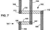
図7は、2つのそのような典型的なコネクタ、即ち、コネクタ101及びコネックタ102を示している。コネクタ101は、第1レベルに位置付けられたトレース103、104及び第2レベルに位置付けられたトレース105から構成される。トレース103はビアホール106によりトレース105に接続され、トレース105はビアホール107によりトレース104に接続されている。コネクタ102は、第1レベルに位置付けられたトレース108、109と第2レベルに位置付けられたトレース110とから構成されている。トレース108はビアホール111によりトレース110に接続され、トレース110はビアホール112によりトレース109に接続されている。簡便性のために、図7は2つの金属層と1つの種類のビアのみを示している。最新式のASIC(特定用途向け集積回路)CAD技術は、9つの金属層とこれらの9つの導電層に接続する8つのビアの集合とまで支援することができる。しかしながら、本発明の概念は、いずれの数の層に対しても容易に適用されることができる。通常、特定の導電層は、1つの方向であって、水平方向か又は垂直方向のどちらかにおいて接続をルーティングするための“配置及び配線”プログラムにおいて選択される。図10においては、下で更に詳細に説明するように、例えば、上層は垂直方向においてルーティングされ、下層は水平方向においてルーティングされている。
FIG. 7 shows two such typical connectors:
第1実施形態に従って、“配置及び配線”ルーチンは、4つの段階であって:1)金属充填;2)金属層のランダム割合の切断;3)無関係なビアの追加;及び、4)どちらかの金属のどちらかの終端にない一部の不所望のビアの削除;の4つの段階から構成される。 According to the first embodiment, the “place and route” routine is in four stages: 1) metal filling; 2) cutting a random percentage of the metal layer; 3) adding irrelevant vias; and 4) either Removal of some undesired vias not at either end of the metal.
段階1:金属充填
空の空間が層群において金属のストリップにより充填され、その充填操作はコンピュータプログラムにより生成される。コンピュータ生成の無関係な導電ストリップの方向は、“配置及び配線”プロセスにおいて規定される特定の導電層各々の方向選択に従う。無関係な導電ストリップは、好適には、ルーティング金属と同じ幅を有する。それらのストリップは、互いから、又、プロセスデザインルールにおいて指定された距離だけ同じ層のルーティング金属から分離している。
Step 1: A metal filled empty space is filled with metal strips in a layer group, and the filling operation is generated by a computer program. The direction of the computer-generated irrelevant conductive strip follows the direction choice of each specific conductive layer defined in the “place and route” process. The irrelevant conductive strip preferably has the same width as the routing metal. The strips are separated from each other and from the same layer of routing metal by a distance specified in the process design rules.
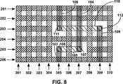
図8はこの第1段階の結果を示す図であり、この図において、コネクタ101(即ち、103−106−105−107−104)及びコネクタ(即ち、108−111−110−112−109)を備える構造は、ここで、更に、第1層における金属の水平方向のストリップ201乃至206及び第2層における金属の垂直方向のストリップ301乃至310から構成される。それらの付加的層は、第1層及び第2層においてオリジナルのルーティングを伴わない空間を充填する。
FIG. 8 shows the result of this first stage, in which the connector 101 (ie, 103-106-105-107-104) and connector (ie, 108-111-110-112-109) are connected. The structure provided here further comprises metal
段階2:導電層のランダム割合切断
第2ソフトウェアルーチンは、グリッドサイズに対比して各々の導電トレースの長さを検出する。グリッドは、導電トレースの中心に正確に位置する想像上の線である。グリッドサイズは、この技術のデザインルールにより指定される2つの隣接する導電コネクタの中心から中心までの一意の距離である。全ての機能性金属及び無関係な金属は、好適には、同じグリッドサイズ(幅に隔たりを加えたもの)を有する。それ故、本段階は、リバースエンジニアが回路における異なるパターンを個別化しようとするとき、彼の作業に負担を課す。
Step 2: Random percentage cutting of the conductive layer The second software routine detects the length of each conductive trace relative to the grid size. The grid is an imaginary line that is precisely located at the center of the conductive trace. The grid size is a unique distance from center to center of two adjacent conductive connectors specified by the design rules of this technology. All functional metals and unrelated metals preferably have the same grid size (width plus spacing). This stage therefore places a burden on his work when the reverse engineer tries to individualize different patterns in the circuit.
導電トレースの長さを検出した後、前の段階において導入された無関係な導電トレースはグリッドサイズに対比して異なるサイズにランダムに切断される。そのランダム性はプログラムにおける擬似ランダム生成サブルーチンにより生成される。このランダム切断の結果として、導電ストリップは、いずれの切断を伴わずに100%損なわれていないものとすることができ、又は、例えば、オリジナルの長さの30%及び70%の2つの部分に若しくは全長の異なる割合を各々が有する更に多くの部分にさえ切断されることができる。例えば、範囲1乃至10における乱数が生成され、生成される第1乱数が4である場合、オリジナルの長さの40%が切断される。次いで、続く乱数が生成され、この乱数が7である場合、残りの長さの70%が切断され、生成される乱数の所定レベルに達するまで、同様に切断される。
After detecting the length of the conductive traces, the extraneous conductive traces introduced in the previous step are randomly cut to a different size compared to the grid size. The randomness is generated by a pseudo-random generation subroutine in the program. As a result of this random cut, the conductive strip can be 100% intact without any cut, or, for example, in two parts, 30% and 70% of the original length. Or it can be cut into even more parts, each having a different proportion of the total length. For example, if random numbers in the
図9は、ランダム割合切断の後の、無関係な導電トレースおよび機能性導電トレースの
パターンを示している。
FIG. 9 shows the pattern of irrelevant and functional conductive traces after random percentage cutting.
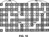
第3段階:無関係なビアの付加
第3のソフトウェアルーチンは、図10に示すように、上層と下層とが重なり合う全ての位置において、図7のビア106、107、111及び112が生成された同じ処理段階を用いて、無関係な接続ビア350を生成する。各々のビアは、製造プロセスの要求のために、デザインルールにより規定される標準的サイズを有している。
Third stage: adding irrelevant vias The third software routine is the same as shown in FIG. 10, where the
図10は、付加的ビアを生成する段階の後の、導電トレース及びビアのパターンを示している。 FIG. 10 shows the pattern of conductive traces and vias after the step of creating additional vias.
第4段階:各々の金属線の各々の終端にない一部の不所望のビアの削除
本物のコネクタのように見える無関係な導電トレース及び無関係な接続ビアを生成するために、前の段階で付加された無関係な接続ビアの一部を削除する必要がある。この理由は、殆どの場合、本物のコネクタは、図7に示すように、金属が終端する位置で2つの導電層を接続するビアを有することである。前の段階においては、ビアは、2つの金属の重なり合った範囲全体に亘って位置付けられている。更なるソフトウェアルーチンがこれらの位置付けられているビアの一部を除去するために用いられる。除去の判断はユーザ指定割合により制御される。例としては、80%が指定されている場合、プログラムは導電トレースの終端において2つのビアを持ち続け、ビアの数字において80%を削除し、その中間の値にする。
Stage 4: Removal of some undesired vias at each end of each metal line Added in the previous stage to create extraneous conductive traces and extraneous connection vias that look like real connectors Need to remove some of the unrelated connection vias. The reason for this is that, in most cases, a real connector has vias connecting the two conductive layers at the location where the metal terminates, as shown in FIG. In the previous stage, the via is located over the entire overlapping area of the two metals. Additional software routines are used to remove some of these positioned vias. The determination of removal is controlled by the user-specified ratio. As an example, if 80% is specified, the program will continue to have two vias at the end of the conductive trace, delete 80% in the via number, and make it an intermediate value.
図11は、導電ストリップの終端において2つのビアの間で充填されたビアの100%が削除された場合について示している。それ故、残されたビアは導電ストリップの終端におけるビアのみである。 FIG. 11 shows the case where 100% of the filled vias between two vias are deleted at the end of the conductive strip. Therefore, the only via left is the via at the end of the conductive strip.
上で説明した第3段階及び第4段階の代替として、無関係な導電線の終端において無関係なビアホールを提供する単一の段階を提供することが可能である。そのような段階においては又、上記の4つの段階の削除ソフトウェアルーチンによりなされる場合と類似して、無関係な導電線の終端において必ずしも位置付けられる必要のないビアホールが提供されることが可能である。 As an alternative to the third and fourth stages described above, it is possible to provide a single stage that provides an irrelevant via hole at the end of an irrelevant conductive line. In such a stage, it is also possible to provide a via hole that does not necessarily have to be located at the end of an irrelevant conductive line, similar to what is done by the four-stage deletion software routine described above.
図7乃至11においては、1つのレベルと他のレベルとの間で区別するために及びオリジナルの金属/ビアと無関係な金属/ビアを区別するために異なるパターンが用いられた。実際のASICにおいては、無関係な金属とオリジナルの金属、無関係なビアとオリジナルのビアは、チップにおいて光学的に区別できない。これについて、図12に示す。図12から、機能性コネクタを充填されたコネクタと区別しようとすることは非常に困難であることが明らかである。 7-11, different patterns were used to distinguish between one level and the other and to distinguish metal / vias that are unrelated to the original metal / via. In an actual ASIC, irrelevant metal and original metal, irrelevant via and original via cannot be optically distinguished on the chip. This is shown in FIG. From FIG. 12, it is clear that it is very difficult to distinguish a functional connector from a filled connector.
図13は、第1の実施形態の詳細のフローチャートを示しており、この図において、S0は初期化操作を示し、S1は第1段階に関連する操作を示し、S2は第2段階に関連する操作を示し、S3は第3段階に関連する操作を示し、及びS4は第4段階に関連する操作を示している。 FIG. 13 shows a detailed flowchart of the first embodiment, in which S0 represents an initialization operation, S1 represents an operation related to the first stage, and S2 represents an operation related to the second stage. S3 indicates an operation related to the third stage, and S4 indicates an operation related to the fourth stage.
第2の実施形態に従って、配置及び配線ルーチンは次のような4段階から構成される。1)基本フィルセル(基本充填セル)をデザインする。2)大きいセルを生成するために基本充填セルを結合させる。3)オリジナルの金属に近過ぎるか又は重なり合っている充填金属を削除する。4)充填金属範囲の正しい層を伴わない充填ビアを削除する。それらの段階について、ここで、更に詳細に説明する。
According to the second embodiment, the placement and wiring routine is composed of the following four stages. 1) Design a basic fill cell (basic filling cell) . 2) Combine basic filling cells to create large cells. 3) Remove filler metal that is too close to or overlapping the original metal. 4) Remove filled vias without the correct layer of filled metal area. These steps will now be described in more detail.
段階1:基本充填セルのデザイン
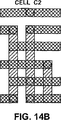
このプロセスの第1段階は、無関係な金属トレースと無関係な接続ビアとから構成される多くの異なる基本セルをデザインするプロセスである。配置及び配線プログラムにおいて生成された機能性導電トレース及び接続ビアから構成される機能性接続は特定の特性を有するため、それらを複製する最善方法は、無関係な金属層及び接続ビアにおいて類似する全ての種類のルーティング構造をマニュアルによりデザインすることである。これらのデザインされる基本セルの数は、例えば、最大30乃至50までとすることができる。図14A乃至14Cは、これらのセルの3つの例を示している。これらのセルの金属及びビアパターンは、それらが配置及び配線プログラムによる機能性接続のようにみえるようにする方法で、意図的にデザインされている。種々の異なる形状のセルが、勿論、本発明を用いた接続において使用されることができ、上記の3つのセルは、例示目的のみで挙げたものである。いずれの種類のセルであって、単一の導電線又は単一のビアホールを有するセルでさえ、デザインすることが可能である。
Stage 1: Basic Fill Cell Design The first stage of this process is the process of designing many different basic cells consisting of irrelevant metal traces and irrelevant connection vias. Functional connections made up of functional conductive traces and connection vias generated in place and route programs have specific characteristics, so the best way to replicate them is to find all similar in unrelated metal layers and connection vias. The type of routing structure is designed manually. The number of designed basic cells can be, for example, up to 30-50. FIGS. 14A-14C show three examples of these cells. The metal and via patterns of these cells are deliberately designed in such a way that they look like functional connections with placement and wiring programs . A variety of differently shaped cells can of course be used in connection using the present invention, and the above three cells are listed for illustrative purposes only. Any type of cell, even a cell with a single conductive line or a single via hole, can be designed.
第2段階:大きいセルを生成するための基本充填セルの結合
この段階においては、前の段階においてデザインされた基本セルは、より大きいセルである次のレベルを生成するために結合される。
Second Stage: Combining Basic Filled Cells to Generate Large Cells In this stage, the basic cells designed in the previous stage are combined to generate the next level, which is a larger cell.
図15はこの第2段階の例を示しており、この図においては、図14A乃至14CのセルC1、C2及びC3は、次のレベルのセルCH1を生成するために互いに隣接されている。最も低いレベルで、全部で30個の異なる基本セルを仮定する場合、3つのセルを互いに隣接させる組み合わせは全部で2700通りあり、異なる高いレベルのセルCH1乃至CH2700を与える。これらの高いレベルのセルにおける無関係な金属トレース及び無関係な接続ビアは、それらが基本セルの複製であるため、機能性ルーティングトレース及びビアに、疑いようもなく非常に似ているように見える。又、次のレベルのセルの幾つかを組み合わせることにより、他の高いレベルにおけるより大きいセルを生成することができる。このようにして繰り返すことにより、無関係な金属及びビアを有するように意図された全体のASICチップの一部をカバーする十分大きいセルが得られる。この最終のセルにおいては、全ての充填金属及びビアは、膨大な数のセルの組み合わせのために、十分なランダム性を有し、同時に、それらは、機能性ルーティングコネクタに非常に類似している。 FIG. 15 shows an example of this second stage, in which cells C1, C2 and C3 of FIGS. 14A-14C are adjacent to each other to generate the next level cell CH1. Assuming a total of 30 different basic cells at the lowest level, there are a total of 2700 combinations of adjoining 3 cells to each other, giving different high level cells CH1 to CH2700. These high levels extraneous metal traces and extraneous connecting vias definitive to cells is that they are for a duplicate of the basic cell, the functional routing traces and vias, appear to be very similar without doubt. Also, some of the next level cells can be combined to produce larger cells at other higher levels. By repeating in this way, a sufficiently large cell is obtained that covers a portion of the entire ASIC chip intended to have extraneous metal and vias. In this final cell, all the filling metal and vias have enough randomness due to the huge number of cell combinations, while at the same time they are very similar to functional routing connectors .
第3段階:機能性導電線に近過ぎるか又は重なり合っている無関係な金属線の削除
更なるソフトウェアルーチンは、次いで、機能性金属線に重なり合っている、あるいは近過ぎる、即ち、デザインルールが許容するより近い、無関係な金属全てを削除する。これは、デザイン上、金属層全てに対してなされる。その結果については図17に示しており、無関係な充填金属のうちの複数の部分が削除されている。
Third stage: Elimination of irrelevant metal lines that are too close to or overlapping the functional conductive lines Further software routines then overlap or close to the functional metal lines , ie the design rules allow closer, remove all extraneous metal. This is done for all metal layers by design. The result is shown in FIG. 17, and a plurality of portions of irrelevant filling metal are deleted.
第4段階:充填金属範囲の正しい層を伴わない無関係なビアの削除
ルーティング金属に近過ぎるか又は接触している充填金属の一部を削除した後、他のソフトウェアルーチンが、前の段階において削除されたカバー金属を有する不必要な接続ビアの処理を行う。適切な無関係な金属トレースのカバーを伴わない不必要なビア全てが、リバースエンジニアの作業に負担を課すように、削除される必要がある。
Step 4: Delete extraneous vias without the correct layer in the fill metal range After deleting some of the fill metal that is too close to or in contact with the routing metal, another software routine deletes it in the previous step Unnecessary connection vias with a covered metal are processed. All unnecessary vias without the appropriate irrelevant metal trace cover need to be removed to place a burden on the reverse engineer's work.
図18は、適切な無関係な金属層のカバーを伴わない無関係なビアが削除された後のルーティング金属及びビアを示している。ルーティングコネクタは、ここで、多くの充填コネクタの間に隠れており、それらは、リバースエンジニアリングの攻撃において識別することは非常に困難である。 FIG. 18 shows the routing metal and vias after the extraneous vias without the appropriate extraneous metal layer cover have been removed. Routing connectors are now hidden among many filling connectors, which are very difficult to identify in reverse engineering attacks.
第1実施形態を参照して既に説明したように、無関係な導電線及び無関係なビアは、機能性導電線及び機能性ビアそれぞれから光学的に区別することはできない。 As already described with reference to the first embodiment, irrelevant conductive lines and irrelevant vias cannot be optically distinguished from functional conductive lines and functional vias, respectively.
図19は、第2実施形態の詳細を示すフローチャートであり、この図において、S10は初期化操作を示し、S11は第1段階に関連する操作を示し、S12は第2段階に関連する操作を示し、S13は第3段階に関連する操作を示し、及びS14は第4段階に関連する操作を示している。 FIG. 19 is a flowchart showing details of the second embodiment. In this figure, S10 shows an initialization operation, S11 shows an operation related to the first stage, and S12 shows an operation related to the second stage. S13 indicates an operation related to the third stage, and S14 indicates an operation related to the fourth stage.
一旦、図12又は18に示す1つのようなレイアウトが得られると、各々の層に対してマスクが調整され、次いで、集積回路を製造するためにファウンドリに送られる。本明細書に示す例においては、3つのマスクが調整される必要があり、それらの1つは上層(機能性導電線及び無関係な導電線)のためのものであり、1つは中間層(機能性ビアホール及び無関係なビアホール)のためのものであり、そして、1つは下層(機能性導電線及び無関係な導電線)のためのものである。マスクの調整段階は、それ自体、既知であり、こここではその詳細説明については省略する。それについては、例えば、参照文献、‘VLSI Technology’,edited by S.M.Sze,McGraw−Hill,1983を参照することができる。 Once a layout such as that shown in FIG. 12 or 18 is obtained, the mask is adjusted for each layer and then sent to the foundry to manufacture the integrated circuit. In the example shown here, three masks need to be adjusted, one of which is for the upper layer (functional conductive line and unrelated conductive line) and one is the intermediate layer ( Functional via holes and unrelated via holes) and one for the lower layer (functional conductive lines and unrelated conductive lines). The adjustment stage of the mask is known per se and its detailed description is omitted here. For example, reference literature, 'VLSI Technology', edited by S. et al. M.M. Reference may be made to Sze, McGraw-Hill, 1983.
本発明については、特定の実施形態を参照して説明したが、本発明の範囲から逸脱することなく、当業者により種々の変形及び変更を実行することができる。それ故、本発明は、同時提出の特許請求の範囲における範囲内の変形及び変更を網羅するように意図されている。 Although the invention has been described with reference to particular embodiments , various modifications and changes can be made by those skilled in the art without departing from the scope of the invention. Therefore, the present invention is intended to cover variations and modifications within the scope of the appended claims.
Claims (30)
該多層集積回路の構成要素間で電気信号を搬送するための、上部導電線を有する上部導電層;
前記集積回路の構成要素間で電気信号を搬送するための、下部導電線を有する下部導電層;及び
前記上部導電線を前記下部導電線と電気的に接続する導電性ビアホールを有する中間層;
を有する多層集積回路であって、
前記上部導電線又は前記下部導電線の何れかのうちの少なくとも1つの導電線は無関係な導電線であり;
前記導電性ビアホールのうちの少なくとも1つのビアホールは無関係なビアホールであり;
前記の少なくとも1つの無関係な導電線は、前記上部及び前記下部導電線の材料と同じ材料から成り;
前記の少なくとも1つの無関係な導電線及び無関係なビアホールは、リバースエンジニアを混乱させるために、無関係な経路を構成し、前記集積回路の動作機能に接続されないようになっており;
前記無関係な導電線及び前記無関係なビアホールは、基本充填セルを形成するように結合されており;且つ
前記基本充填セルは、より大きいセルを形成するように結合されている;
ことを特徴とする多層集積回路。A multilayer integrated circuit:
For conveying electrical signals between components of the multilayer integrated circuits, the upper conductive layer having an upper conductive wire;
Intermediate layer having and conductive via holes for connecting the upper conductive wire in the lower conductive wire and electrically; the between components of an integrated circuit for carrying electrical signals, the lower conductive layer to have a lower conductive wire;
A multi-layer integrated circuit comprising:
At least one conductive line of any one of the upper conductive wire or the lower conductive line is an independent conductive lines;
At least one via hole of the conductive via is unrelated via hole;
The at least one unrelated conductive line is made of the same material as the material of the upper and lower conductive lines ;
At least one extraneous conductive lines and extraneous via holes of said, to confuse a reverse engineer, constitute independent paths, and so as not to be connected to the operating function of said integrated circuit;
The extraneous conductive lines and the extraneous via holes are coupled to form a basic fill cell; and
The basic filling cells are combined to form larger cells;
A multilayer integrated circuit characterized by the above.
前記上部導電線が位置している上部ルーティングチャネル;及び
前記下部導電線が位置している下部ルーティングチャネル;
を更に有し、
前記少なくとも1つの無関係な導電線は前記ルーティングチャネルの少なくとも1つに位置している;
ことを特徴とする多層集積回路。A multilayer integrated circuit according to claim 1, wherein the extraneous conductive lines have the same dimensions as the upper and lower conductive lines, and / or, the multilayer integrated circuits is:
An upper routing channel in which the upper conductive line is located; and a lower routing channel in which the lower conductive line is located;
Further comprising
The at least one extraneous conductive line is located in at least one of the routing channels;
A multilayer integrated circuit characterized by the above.
前記集積回路の構成要素間で電気信号を搬送するための上部導電線を有する上部導電層を形成する段階;
前記集積回路の構成要素間で電気信号を搬送するための下部導電線を有する下部導電層を形成する段階;
前記上部導電線を前記下部導電線と電気的に接続するビアホールを有する中間層を形成する段階;並びに
基本充填セルを形成する段階であり、該基本充填セルは:
前記上部導電層と前記下部導電層とのうちの少なくとも1つの導電層内の無関係な導電線であり、前記上部及び下部導電線の材料と同じ材料から成る無関係な導電線;及び
前記ビアホールのうちの無関係なビアホール;
を有し、
前記無関係な導電線及び前記無関係なビアホールは、リバースエンジニアを混乱させるために、無関係な経路を構成し、前記集積回路の動作機能に接続されないようになっている;
基本充填セルを形成する段階;
を有し、
前記基本充填セルは、より大きいセルを形成するように結合される;
ことを特徴とするプロセス。 A process for manufacturing a multilayer integrated circuit comprising:
Forming an upper conductive layer having an upper conductive lines for conveying electrical signals between components of the integrated circuit;
Forming a lower conductive layer having a lower conductive lines for conveying electrical signals between components of the integrated circuit;
Forming an intermediate layer having a via hole electrically connecting the upper conductive line to the lower conductive line; and
Forming a basic filling cell, the basic filling cell comprising:
Wherein at least one extraneous conductive lines in the conductive layer of the upper conductive layer and the lower conductive layer, extraneous conductive lines made of the same material as the material of the upper and lower conductive lines; and
An unrelated via hole among the via holes;
I have a,
The extraneous conductive lines and said extraneous via holes, to confuse a reverse engineer, constitute independent pathways, so as not connected to the operating function of said integrated circuit;
Forming a basic filling cell;
Have
The basic filling cells are combined to form larger cells;
Process characterized by that.
前記上部導電線が位置している上部ルーティングチャネル;及び
前記下部導電線が位置している下部ルーティングチャネル;
を更に有し、
前記無関係な導電線は前記ルーティングチャネルの少なくとも1つに位置している;
ことを特徴とするプロセス。A process according to claim 9, wherein the extraneous conductive lines have the same dimensions as the upper and lower conductive lines, and / or, the multilayer integrated circuits is:
An upper routing channel in which the upper conductive line is located; and a lower routing channel in which the lower conductive line is located;
Further comprising
Before cinchona relation conductive lines are located on at least one of said routing channel;
Process characterized by that.
前記電気回路の構成要素間で電気信号を搬送するための第1層機能導電線を有する第1導電層の表現を与える段階;
前記電気回路の構成要素間で電気信号を搬送するための第2層機能導電線を有する第2導電層の表現を与える段階;
前記第1層機能導電線を前記第2層機能導電線に電気的に接続する機能ビアホールの表現を与える段階;
前記第1導電層と前記第2導電層とのうちの少なくとも1層に挿入される無関係な導電線の表現を与える段階;
前記無関係な導電線に電気的に接続された無関係なビアホールの表現を与える段階であり、前記無関係な導電線及び無関係なビアホールは、リバースエンジニアを混乱させるために、無関係な経路を形成するようにデザインされ、前記回路の動作機能に接続されてない、段階;
各基本充填セルが少なくとも1つの無関係な導電線又は少なくとも1つの無関係なビアを有する基本充填セルの表現を与える段階;及び
より大きいセルを形成するように前記基本充填セルを結合する表現を与える段階;
を有することを特徴とする方法。A method of designing a multi-layer electric circuit having a function conductive lines and extraneous conductive lines for transmission of electric signals, the designed multi-layer electrical circuit suitable for making multi-layer electrical circuit of the corresponding three-dimensional There is a way:
Step of providing a representation of first conductive layer having a first layer functions conductive line for conveying electrical signals between components of the electrical circuit;
Step of providing a representation of the second conductive layer having a second layer functional conductive lines for conveying electrical signals between components of the electrical circuit;
Providing a representation of a functional via hole that electrically connects the first layer functional conductive line to the second layer functional conductive line;
Step of providing a representation of extraneous conductive lines to be inserted into at least one layer of the second conductive layer and the first conductive layer;
A step of providing an electrically connected unrelated hole representation to the extraneous conductive lines, the extraneous conductive lines and independent via holes, to confuse a reverse engineer, so as to form independent pathways designed, have Na is connected to the operating functions of the circuit, step;
Providing a representation of a basic fill cell with each basic fill cell having at least one extraneous conductive line or at least one extraneous via; and
Providing an expression that combines the basic filled cells to form larger cells;
Method characterized by having a.
該電気回路の構成要素間で電気信号を搬送するための機能導電線を備える段階;
前記機能導電線の電気接続のための機能ビアホールを備える段階;
無関係な導電線を備える段階であって、前記無関係な導電線は前記電気回路の動作に対して不必要な機能を実行する、段階;並びに
前記の無関係な導電線の電気接続のために無関係なビアホールを備える段階であって、前記無関係な導電線及び無関係なビアホールは、リバースエンジニアを混乱させるために、無関係な経路を構成し、前記回路の動作機能に接続されない、段階;
を有し、
前記無関係な導電線及び前記無関係なビアホールは、基本充填セルを形成するように結合され;且つ
前記基本充填セルは、より大きいセルを形成するように結合される;
プロセス。A process for manufacturing an electrical circuit comprising:
Step of providing the functions conductive lines for conveying electrical signals between components of the electrical circuits;
Providing a functional via hole for electrical connection of the functional conductive line;
Providing an irrelevant conductive line, said irrelevant conductive line performing an unnecessary function for the operation of said electrical circuit; and irrelevant for electrical connection of said irrelevant conductive line a step of providing a via hole, the extraneous conductive lines and independent via holes, to confuse a reverse engineer, configures the irrelevant path, have such connected to the operating functions of the circuit, step;
I have a,
The extraneous conductive lines and the extraneous via holes are combined to form a basic fill cell; and
The basic filling cells are combined to form larger cells;
process.
Applications Claiming Priority (3)
| Application Number | Priority Date | Filing Date | Title |
|---|---|---|---|
| US42017302P | 2002-10-21 | 2002-10-21 | |
| US10/686,545 US6924552B2 (en) | 2002-10-21 | 2003-10-14 | Multilayered integrated circuit with extraneous conductive traces |
| PCT/US2003/032961 WO2004038800A2 (en) | 2002-10-21 | 2003-10-16 | Multilayered integrated circuit with non functional conductive traces |
Publications (3)
| Publication Number | Publication Date |
|---|---|
| JP2006517053A JP2006517053A (en) | 2006-07-13 |
| JP2006517053A5 JP2006517053A5 (en) | 2006-12-07 |
| JP4642471B2 true JP4642471B2 (en) | 2011-03-02 |
Family
ID=32179786
Family Applications (1)
| Application Number | Title | Priority Date | Filing Date |
|---|---|---|---|
| JP2004546897A Expired - Fee Related JP4642471B2 (en) | 2002-10-21 | 2003-10-16 | Multilayer integrated circuit with unrelated conductive traces. |
Country Status (6)
| Country | Link |
|---|---|
| US (1) | US6924552B2 (en) |
| JP (1) | JP4642471B2 (en) |
| AU (1) | AU2003284270A1 (en) |
| GB (1) | GB2411293B (en) |
| TW (2) | TWI327368B (en) |
| WO (1) | WO2004038800A2 (en) |
Families Citing this family (31)
| Publication number | Priority date | Publication date | Assignee | Title |
|---|---|---|---|---|
| JP3986989B2 (en) * | 2003-03-27 | 2007-10-03 | 松下電器産業株式会社 | Semiconductor device |
| JP2007528121A (en) * | 2003-07-11 | 2007-10-04 | コーニンクレッカ フィリップス エレクトロニクス エヌ ヴィ | Semiconductor products that require confidentiality, especially smart card chips |
| WO2005117115A1 (en) * | 2004-05-28 | 2005-12-08 | Koninklijke Philips Electronics N.V. | Chips with useful lines and dummy lines |
| US8168487B2 (en) * | 2006-09-28 | 2012-05-01 | Hrl Laboratories, Llc | Programmable connection and isolation of active regions in an integrated circuit using ambiguous features to confuse a reverse engineer |
| US7723998B2 (en) | 2007-06-12 | 2010-05-25 | Itt Manufacturing Enterprises, Inc. | Integrated circuit protection and detection grid |
| US7994042B2 (en) | 2007-10-26 | 2011-08-09 | International Business Machines Corporation | Techniques for impeding reverse engineering |
| KR101383704B1 (en) * | 2008-01-18 | 2014-04-10 | 삼성디스플레이 주식회사 | Circuit board and display device including the same |
| US7709401B2 (en) * | 2008-02-22 | 2010-05-04 | International Business Machines Corporation | Method of making thermally programmable anti-reverse engineering interconnects wherein interconnects only conduct when heated above room temperature |
| US8151235B2 (en) * | 2009-02-24 | 2012-04-03 | Syphermedia International, Inc. | Camouflaging a standard cell based integrated circuit |
| US10691860B2 (en) | 2009-02-24 | 2020-06-23 | Rambus Inc. | Secure logic locking and configuration with camouflaged programmable micro netlists |
| US9735781B2 (en) | 2009-02-24 | 2017-08-15 | Syphermedia International, Inc. | Physically unclonable camouflage structure and methods for fabricating same |
| US8418091B2 (en) | 2009-02-24 | 2013-04-09 | Syphermedia International, Inc. | Method and apparatus for camouflaging a standard cell based integrated circuit |
| US8510700B2 (en) | 2009-02-24 | 2013-08-13 | Syphermedia International, Inc. | Method and apparatus for camouflaging a standard cell based integrated circuit with micro circuits and post processing |
| US8111089B2 (en) * | 2009-05-28 | 2012-02-07 | Syphermedia International, Inc. | Building block for a secure CMOS logic cell library |
| US9218511B2 (en) * | 2011-06-07 | 2015-12-22 | Verisiti, Inc. | Semiconductor device having features to prevent reverse engineering |
| FR3007198B1 (en) | 2013-06-13 | 2015-06-19 | St Microelectronics Rousset | COMPONENT, FOR EXAMPLE NMOS TRANSISTOR, ACTIVE REGION WITH RELEASED COMPRESSION STRESSES, AND METHOD OF MANUFACTURING |
| US9479176B1 (en) | 2013-12-09 | 2016-10-25 | Rambus Inc. | Methods and circuits for protecting integrated circuits from reverse engineering |
| FR3018139B1 (en) | 2014-02-28 | 2018-04-27 | Stmicroelectronics (Rousset) Sas | COMPONENT INTEGRATED CIRCUIT, FOR EXAMPLE NMOS TRANSISTORS, WITH ACTIVATED REGIONS WITH COMPRESSED COMPRESSION STRESSES |
| FR3025335B1 (en) | 2014-08-29 | 2016-09-23 | Stmicroelectronics Rousset | METHOD FOR MANUFACTURING AN INTEGRATED CIRCUIT FOR IMPROVING INTEGRATED CIRCUIT RETRO-DESIGN AND CORRESPONDING INTEGRATED CIRCUIT |
| JP6390299B2 (en) * | 2014-09-18 | 2018-09-19 | 富士通セミコンダクター株式会社 | Integrated circuit device design method, integrated circuit device manufacturing method, and integrated circuit device |
| WO2016180977A1 (en) * | 2015-05-13 | 2016-11-17 | Nagravision S.A. | Integrated circuit chip protection against physical and/or electrical alterations |
| WO2018106233A1 (en) * | 2016-12-07 | 2018-06-14 | Intel Corporation | Integrated circuit device with crenellated metal trace layout |
| JP7048182B2 (en) | 2016-08-26 | 2022-04-05 | インテル・コーポレーション | Integrated circuit device structure and double-sided manufacturing technology |
| US10262956B2 (en) | 2017-02-27 | 2019-04-16 | Cisco Technology, Inc. | Timing based camouflage circuit |
| US10381315B2 (en) | 2017-11-16 | 2019-08-13 | Samsung Electronics Co., Ltd. | Method and system for providing a reverse-engineering resistant hardware embedded security module |
| WO2019132863A1 (en) | 2017-12-26 | 2019-07-04 | Intel Corporation | Stacked transistors with contact last |
| US11430814B2 (en) | 2018-03-05 | 2022-08-30 | Intel Corporation | Metallization structures for stacked device connectivity and their methods of fabrication |
| US10923596B2 (en) | 2019-03-08 | 2021-02-16 | Rambus Inc. | Camouflaged FinFET and method for producing same |
| US11688780B2 (en) | 2019-03-22 | 2023-06-27 | Intel Corporation | Deep source and drain for transistor structures with back-side contact metallization |
| WO2022161590A1 (en) | 2021-01-26 | 2022-08-04 | Tallinn University Of Technology | Physical obfuscation of hardware through capacitive coupling |
| US20230139843A1 (en) * | 2021-11-03 | 2023-05-04 | Taiwan Semiconductor Manufacturing Company, Ltd. | Semiconductor devices and methods of manufacturing thereof |
Citations (4)
| Publication number | Priority date | Publication date | Assignee | Title |
|---|---|---|---|---|
| JP2000101055A (en) * | 1998-09-25 | 2000-04-07 | Seiko Epson Corp | Semiconductor device |
| JP2001035853A (en) * | 1999-05-17 | 2001-02-09 | Seiko Epson Corp | Semiconductor device and fabrication thereof |
| JP2001284357A (en) * | 2000-03-30 | 2001-10-12 | Sony Corp | Semiconductor device |
| WO2002043147A1 (en) * | 2000-11-23 | 2002-05-30 | Infineon Technologies Ag | Integrated circuit configuration that is protected against analysis, and method for producing the configuration |
Family Cites Families (9)
| Publication number | Priority date | Publication date | Assignee | Title |
|---|---|---|---|---|
| IL106513A (en) * | 1992-07-31 | 1997-03-18 | Hughes Aircraft Co | Integrated circuit security system and method with implanted interconnections |
| US5783846A (en) * | 1995-09-22 | 1998-07-21 | Hughes Electronics Corporation | Digital circuit with transistor geometry and channel stops providing camouflage against reverse engineering |
| JPH10270562A (en) * | 1997-03-27 | 1998-10-09 | Nippon Telegr & Teleph Corp <Ntt> | Semiconductor integrated circuit |
| US5973375A (en) * | 1997-06-06 | 1999-10-26 | Hughes Electronics Corporation | Camouflaged circuit structure with step implants |
| US6117762A (en) * | 1999-04-23 | 2000-09-12 | Hrl Laboratories, Llc | Method and apparatus using silicide layer for protecting integrated circuits from reverse engineering |
| US6207479B1 (en) * | 1999-06-14 | 2001-03-27 | Taiwan Semiconductor Manufacturing Co., Ltd. | Place and route method for integrated circuit design |
| TW515073B (en) * | 1999-11-15 | 2002-12-21 | Winbond Electronics Corp | Method for generating virtual metal pattern layer |
| JP4553461B2 (en) * | 2000-08-23 | 2010-09-29 | ルネサスエレクトロニクス株式会社 | Semiconductor device, design method thereof and design apparatus |
| EP1193758A1 (en) | 2000-10-02 | 2002-04-03 | STMicroelectronics S.r.l. | Anti-deciphering contacts |
-
2003
- 2003-10-14 US US10/686,545 patent/US6924552B2/en not_active Expired - Fee Related
- 2003-10-16 WO PCT/US2003/032961 patent/WO2004038800A2/en active Application Filing
- 2003-10-16 AU AU2003284270A patent/AU2003284270A1/en not_active Abandoned
- 2003-10-16 JP JP2004546897A patent/JP4642471B2/en not_active Expired - Fee Related
- 2003-10-16 GB GB0510347A patent/GB2411293B/en not_active Expired - Fee Related
- 2003-10-20 TW TW099100163A patent/TWI327368B/en not_active IP Right Cessation
- 2003-10-20 TW TW092129023A patent/TWI326485B/en not_active IP Right Cessation
Patent Citations (4)
| Publication number | Priority date | Publication date | Assignee | Title |
|---|---|---|---|---|
| JP2000101055A (en) * | 1998-09-25 | 2000-04-07 | Seiko Epson Corp | Semiconductor device |
| JP2001035853A (en) * | 1999-05-17 | 2001-02-09 | Seiko Epson Corp | Semiconductor device and fabrication thereof |
| JP2001284357A (en) * | 2000-03-30 | 2001-10-12 | Sony Corp | Semiconductor device |
| WO2002043147A1 (en) * | 2000-11-23 | 2002-05-30 | Infineon Technologies Ag | Integrated circuit configuration that is protected against analysis, and method for producing the configuration |
Also Published As
| Publication number | Publication date |
|---|---|
| GB2411293B (en) | 2006-07-12 |
| AU2003284270A8 (en) | 2004-05-13 |
| GB0510347D0 (en) | 2005-06-29 |
| JP2006517053A (en) | 2006-07-13 |
| GB2411293A (en) | 2005-08-24 |
| TWI327368B (en) | 2010-07-11 |
| TW201023329A (en) | 2010-06-16 |
| US6924552B2 (en) | 2005-08-02 |
| WO2004038800A3 (en) | 2004-06-10 |
| US20040119165A1 (en) | 2004-06-24 |
| WO2004038800A2 (en) | 2004-05-06 |
| TWI326485B (en) | 2010-06-21 |
| TW200418162A (en) | 2004-09-16 |
| AU2003284270A1 (en) | 2004-05-13 |
Similar Documents
| Publication | Publication Date | Title |
|---|---|---|
| JP4642471B2 (en) | Multilayer integrated circuit with unrelated conductive traces. | |
| US9563731B2 (en) | Cell boundaries for self aligned multiple patterning abutments | |
| US9947645B2 (en) | Multi-project wafer with IP protection by reticle mask pattern modification | |
| US7424695B2 (en) | Method of manufacturing a semiconductor integrated circuit, a program for a computer automated design system, and a semiconductor integrated circuit | |
| US8516428B2 (en) | Methods, systems, and media to improve manufacturability of semiconductor devices | |
| US7323768B2 (en) | Voltage contrast monitor for integrated circuit defects | |
| US20050141764A1 (en) | Pattern analysis method and pattern analysis apparatus | |
| US7498250B2 (en) | Shapes-based migration of aluminum designs to copper damascene | |
| US20040044983A1 (en) | Method of using filller metal for implementing changes in an integrated circuit design | |
| US20080142987A1 (en) | Computer automated design system, a computer automated design method, and a semiconductor integrated circuit | |
| US6791191B2 (en) | Integrated circuits protected against reverse engineering and method for fabricating the same using vias without metal terminations | |
| US7681168B2 (en) | Semiconductor integrated device, method of designing semiconductor integrated device, device for designing the same, and program | |
| US6528883B1 (en) | Shapes-based migration of aluminum designs to copper damascene | |
| US6097884A (en) | Probe points and markers for critical paths and integrated circuits | |
| US20080197449A1 (en) | Wiring structure of semiconductor integrated circuit device, and method and device for designing the same | |
| US6864171B1 (en) | Via density rules | |
| JP2004235333A (en) | Method of layout of semiconductor integrated circuit and manufacturing method of semiconductor integrated circuit using the method of layout | |
| JP6836137B2 (en) | Semiconductor device and its layout design method | |
| JP3611202B2 (en) | Non-rectangular LSI layout method | |
| JP2005322785A (en) | Semiconductor integrated circuit and pattern formation method thereof | |
| JPH06216249A (en) | Automatic layout design system for ic chip | |
| JP2002366599A (en) | Method for generating flattened pattern | |
| JPH10125795A (en) | Layout design method of semiconductor integrated circuit and recording medium | |
| JP2005142376A (en) | Semiconductor device and method for analyzing the same | |
| JPS6366424B2 (en) |
Legal Events
| Date | Code | Title | Description |
|---|---|---|---|
| A521 | Request for written amendment filed |
Free format text: JAPANESE INTERMEDIATE CODE: A523 Effective date: 20061016 |
|
| A621 | Written request for application examination |
Free format text: JAPANESE INTERMEDIATE CODE: A621 Effective date: 20061016 |
|
| A977 | Report on retrieval |
Free format text: JAPANESE INTERMEDIATE CODE: A971007 Effective date: 20090827 |
|
| A131 | Notification of reasons for refusal |
Free format text: JAPANESE INTERMEDIATE CODE: A131 Effective date: 20100706 |
|
| A521 | Request for written amendment filed |
Free format text: JAPANESE INTERMEDIATE CODE: A523 Effective date: 20100927 |
|
| TRDD | Decision of grant or rejection written | ||
| A01 | Written decision to grant a patent or to grant a registration (utility model) |
Free format text: JAPANESE INTERMEDIATE CODE: A01 Effective date: 20101109 |
|
| A01 | Written decision to grant a patent or to grant a registration (utility model) |
Free format text: JAPANESE INTERMEDIATE CODE: A01 |
|
| A61 | First payment of annual fees (during grant procedure) |
Free format text: JAPANESE INTERMEDIATE CODE: A61 Effective date: 20101201 |
|
| R150 | Certificate of patent or registration of utility model |
Free format text: JAPANESE INTERMEDIATE CODE: R150 |
|
| FPAY | Renewal fee payment (event date is renewal date of database) |
Free format text: PAYMENT UNTIL: 20131210 Year of fee payment: 3 |
|
| R250 | Receipt of annual fees |
Free format text: JAPANESE INTERMEDIATE CODE: R250 |
|
| R250 | Receipt of annual fees |
Free format text: JAPANESE INTERMEDIATE CODE: R250 |
|
| LAPS | Cancellation because of no payment of annual fees |