JP4641478B2 - Optical scanning device and image forming apparatus using the same - Google Patents
Optical scanning device and image forming apparatus using the same Download PDFInfo
- Publication number
- JP4641478B2 JP4641478B2 JP2005280432A JP2005280432A JP4641478B2 JP 4641478 B2 JP4641478 B2 JP 4641478B2 JP 2005280432 A JP2005280432 A JP 2005280432A JP 2005280432 A JP2005280432 A JP 2005280432A JP 4641478 B2 JP4641478 B2 JP 4641478B2
- Authority
- JP
- Japan
- Prior art keywords
- light
- optical system
- light source
- light beam
- deflecting
- Prior art date
- Legal status (The legal status is an assumption and is not a legal conclusion. Google has not performed a legal analysis and makes no representation as to the accuracy of the status listed.)
- Expired - Fee Related
Links
Images


Classifications
-
- G—PHYSICS
- G02—OPTICS
- G02B—OPTICAL ELEMENTS, SYSTEMS OR APPARATUS
- G02B26/00—Optical devices or arrangements for the control of light using movable or deformable optical elements
- G02B26/08—Optical devices or arrangements for the control of light using movable or deformable optical elements for controlling the direction of light
- G02B26/10—Scanning systems
- G02B26/12—Scanning systems using multifaceted mirrors
- G02B26/127—Adaptive control of the scanning light beam, e.g. using the feedback from one or more detectors
Description
本発明は光走査装置及びそれを用いた画像形成装置に関し、例えば電子写真プロセスを有するレーザービームプリンタやデジタル複写機、マルチファンクションプリンタ(多機能プリンタ)等の画像形成装置に好適なものである。 The present invention relates to an optical scanning device and an image forming apparatus using the same, and is suitable for an image forming apparatus such as a laser beam printer, a digital copying machine, or a multi-function printer (multi-function printer) having an electrophotographic process.
従来よりレーザービームプリンター(LBP)等の光走査装置においては画像信号に応じて光源手段から光変調され出射した光束を、例えば回転多面鏡(ポリゴンミラー)より成る光偏向器により周期的に偏向させる。そして偏向された光束をfθ特性を有する走査光学系(結像光学系)によって感光性の記録媒体(感光ドラム)面上にスポット状に集束させ、その面上を光走査して画像記録を行っている。 2. Description of the Related Art Conventionally, in an optical scanning device such as a laser beam printer (LBP), a light beam modulated and emitted from a light source unit according to an image signal is periodically deflected by an optical deflector composed of, for example, a rotating polygon mirror. . The deflected light beam is focused in a spot shape on the surface of a photosensitive recording medium (photosensitive drum) by a scanning optical system (imaging optical system) having fθ characteristics, and image recording is performed by optically scanning the surface. ing.
図16は従来の光走査装置の要部概略図である。 FIG. 16 is a schematic view of a main part of a conventional optical scanning device.
同図において光源手段81から出射した発散光束はコリメータレンズ83により略平行光束に変換され、絞り82によって該光束を制限して副走査方向にのみ所定の屈折力を有するシリンドリカルレンズ84に入射している。シリンドリカルレンズ84に入射した略平行光束のうち主走査断面内においてはそのままの状態で射出する。また副走査断面内においては集束して回転多面鏡から成る偏向手段85の偏向面(反射面)85aにほぼ線像として結像している。
In the figure, a divergent light beam emitted from a light source means 81 is converted into a substantially parallel light beam by a
そして偏向手段85の偏向面85aで偏向された光束を結像光学系86を介して被走査面としての感光ドラム面87上に導光する。そして偏向手段85を矢印A方向に回転させることによって該感光ドラム面87上を矢印B方向に光走査して画像情報の記録を行なっている。
Then, the light beam deflected by the deflecting surface 85 a of the
上記の光走査装置においては感光ドラム面87上を光スポットで走査する前に該感光ドラム87面上における画像形成を開始するタイミングを調整するために、光検出器としてのBD(beam detector)センサ−89が設けられている。このBDセンサー89は光偏向器85で反射偏向された光束の一部であるBD光束、即ち感光ドラム面87上の画像形成領域を走査する前の画像形成領域外の領域を走査しているときの光束を受光する。このBD光束はBDミラー88で反射され、BDレンズ(不図示)で集光されてBDセンサー89に入射する。そしてこのBDセンサー89の出力信号からBD信号(同期信号)を検出し画像処理部91に入力されて、画像走査用の画像クロックと同期を取り、画像記録開始のタイミング制御を行う。
In the above optical scanning device, a BD (beam detector) sensor as a photodetector is used to adjust the timing for starting image formation on the surface of the
そして画像処理部91に入力された画像信号は画像書き込み開始が制御されたタイミングにより画像クロックに従って半導体レーザー駆動部92に出力され、上述した経路でレーザー偏向走査が実行される。また半導体レーザー81内部のレーザー近傍付近に配置されたフォトダイオードからの情報を検出し、この情報から半導体レーザー81の出射パワーが標準光量となるようにAPC(Automatic Power Control)制御がなされる。
The image signal input to the
しかしながら、APCにより半導体レーザー81の発光量を一定にするフィードバック制御は、あくまで該半導体レーザ−81の素子チップ面上で所定の標準光量(標準パワー)が得られるような動作である。
However, the feedback control for making the light emission amount of the
一方、電子写真プロセスにおいて実際に必要とされるのは、感光ドラム面上の光量(パワー)である。ところが必ずしもAPC動作だけでは、感光ドラム面上の光量の経時的な劣化に対する保証はされない。 On the other hand, what is actually required in the electrophotographic process is the amount of light (power) on the surface of the photosensitive drum. However, the APC operation alone does not necessarily guarantee against deterioration over time of the light amount on the photosensitive drum surface.
図17に波長による一般の硝材の透過率特性を示す。同図に示すように一般的に赤外領域から可視の450nm付近までは90%以上のほぼ一定の透過率を示している。しかしながら、一般にガラスは紫外領域で光を吸収してしまうため、透過できる光の波長には下限(吸収端)が存在する。同図に示すように波長450nmより波長が短くなる領域においては急激に透過率が低下しているのが分かる。 FIG. 17 shows transmittance characteristics of a general glass material according to wavelength. As shown in the figure, generally, a substantially constant transmittance of 90% or more is shown from the infrared region to the visible vicinity of 450 nm. However, since glass generally absorbs light in the ultraviolet region, there is a lower limit (absorption edge) for the wavelength of light that can be transmitted. As shown in the figure, it can be seen that in the region where the wavelength is shorter than the wavelength of 450 nm, the transmittance sharply decreases.
ところで、近年ではさらなる印字の高精度が求められている。最近ではブルーレーザー(青紫色の半導体レーザー)など波長450nm以下の短波長の光を放射する光源を用いた光走査装置が種々と提案されている(特許文献1参照)。 Incidentally, in recent years, there has been a demand for higher printing accuracy. Recently, various optical scanning devices using a light source that emits light with a short wavelength of 450 nm or less such as a blue laser (blue-violet semiconductor laser) have been proposed (see Patent Document 1).
特許文献1では波長450nm以下の短波長の光を放射する光源を使うことで、光走査装置が被走査面上に形成する光スポットを小径化して印字の高精彩化を図っている。
しかしながら、波長450nm以下の波長領域においては上述したように半導体レーザーの波長変化に対する硝材の透過率変化が従来の赤外領域に比べて大きい。したがって、温度変化などの環境要因のためレーザーの発信波長が変化した場合、APC動作により半導体レーザーの発光量を一定にしても各光学素子の透過率が変化するために感光ドラム面上の光量が一定にならない。その結果、画像の再現性を良好に維持できないという問題点が生じてしまう。
However, in the wavelength region of
本発明は環境変動や波長変動に対して感光ドラム面上の光量変動を防止し、画像の再現性を良好に維持すると共に、高精彩な画質を満足させることができる光走査装置及びそれを用いた画像形成装置の提供を目的とする。 The present invention prevents an optical fluctuation on the surface of a photosensitive drum against environmental fluctuations and wavelength fluctuations, maintains an excellent image reproducibility, and can satisfy a high-definition image quality, and an optical scanning apparatus using the same. An object of the present invention is to provide an image forming apparatus.
請求項1の発明の光走査装置は、波長が450nm以下の光束を出射する光源手段と、前記光源手段から出射した光束を偏向走査する偏向手段に入射させる入射光学系と、前記偏向手段の偏向面で偏向走査された光束を被走査面上に結像させる結像光学系とを具備する光走査装置において、
前記光源手段から出射された光束の波長変動に伴う前記入射光学系と前記結像光学系の分光透過率の変動を検出する光量検知手段と、
前記光量検知手段で検知された検出値に基づいて前記光源手段の出力を制御する制御手段と、を有し、
前記光量検知手段は、前記被走査面と共役の位置に配置され、前記光量検知手段は、前記入射光学系及び前記偏向手段及び前記結像光学系を通過した光束を検知しており、
前記制御手段は、温度変化があったとき、前記光源手段の出力を変化させることを特徴としている。
Optical scanning apparatus of the invention of
A light amount detecting means for detecting a change in spectral transmittance of the incident optical system and the imaging optical system accompanying a wavelength fluctuation of a light beam emitted from the light source means;
Control means for controlling the output of the light source means based on the detection value detected by the light quantity detection means,
The light amount detecting means is disposed at a position conjugate with the surface to be scanned, and the light amount detecting means detects a light beam that has passed through the incident optical system, the deflecting means, and the imaging optical system,
The control means changes the output of the light source means when there is a temperature change.
請求項2の発明の光走査装置は、波長が450nm以下の光束を出射する光源手段と、前記光源手段から出射した光束を偏向走査する偏向手段に入射させる入射光学系と、前記偏向手段の偏向面で偏向走査された光束を被走査面上に結像させる結像光学系とを具備する光走査装置において、
前記結像光学系を構成する屈折光学素子はアッベ数が40以上の材料より成り、
前記光源手段から出射された光束の波長変動に伴う前記入射光学系の分光透過率の変動を検出する光量検知手段と、
前記光量検知手段で検知された検出値に基づいて前記光源手段の出力を制御する制御手段と、を有し、
前記光量検知手段は、前記入射光学系及び前記偏向手段を通過した光束を検知しており、
前記制御手段は、温度変化があったとき、前記光源手段の出力を変化させることを特徴としている。
Optical scanning apparatus of the invention of
The refractive optical element constituting the imaging optical system is made of a material having an Abbe number of 40 or more,
A light amount detecting means for detecting a change in spectral transmittance of the incident optical system accompanying a wavelength fluctuation of a light beam emitted from the light source means;
Control means for controlling the output of the light source means based on the detection value detected by the light quantity detection means,
The light amount detection means detects a light beam that has passed through the incident optical system and the deflection means,
Wherein, when a temperature change is characterized by changing the output of said light source means.
請求項3の発明の光走査装置は、波長が450nm以下の光束を出射する光源手段と、前記光源手段から出射した光束を偏向走査する偏向手段に入射させる入射光学系と、前記偏向手段の偏向面で偏向走査された光束を被走査面上に結像させる結像光学系とを具備する光走査装置において、
前記光源手段から出射した光束の一部を分割する光分割手段と、前記光分割手段で分割された光束を検出する光量検知手段と、前記光分割手段と前記光量検知手段との間に配置した補正板と、を有し、
前記補正板は、前記光源手段から出射された光束の波長変動に伴う前記入射光学系と前記結像光学系の分光透過率の変動と同一又は比例する光学特性を有しており、
温度変化があったとき、前記光量検知手段で検知された検出値に基づいて、前記光源手段の出力を変化させる制御手段を有することを特徴としている。
According to a third aspect of the present invention, there is provided an optical scanning device comprising: a light source unit that emits a light beam having a wavelength of 450 nm or less; an incident optical system that causes the light beam emitted from the light source unit to be incident on a deflecting unit that scans and deflects; In an optical scanning device comprising an imaging optical system that forms an image of a light beam deflected and scanned on a surface on a surface to be scanned ,
Light splitting means for splitting a part of the light beam emitted from the light source means, light quantity detection means for detecting the light flux split by the light splitting means, and disposed between the light splitting means and the light quantity detection means A correction plate,
The correction plate has an optical characteristic that is the same as or proportional to a change in spectral transmittance of the incident optical system and the imaging optical system due to a change in wavelength of the light beam emitted from the light source means,
It has a control means for changing the output of the light source means based on the detection value detected by the light quantity detection means when there is a temperature change.
請求項4の発明の光走査装置は、波長が450nm以下の光束を出射する光源手段と、前記光源手段から出射した光束を偏向走査する偏向手段に入射させる入射光学系と、前記偏向手段の偏向面で偏向走査された光束を被走査面上に結像させる結像光学系とを具備する光走査装置において、
前記光源手段から出射した光束の一部を分割する光分割手段と、前記光分割手段で分割された光束を検出する光量検知手段と、を有し、
前記光量検知手段は、前記光源手段から出射された光束の波長変動に伴う前記入射光学系と前記結像光学系の分光透過率の変動と同一又は比例する感度特性を有しており、
温度変化があったとき、前記光量検知手段で検知された検出値に基づいて、前記光源手段の出力を変化させる制御手段を有することを特徴としている。
Optical scanning apparatus of the invention of
A light splitting unit that splits a part of the light beam emitted from the light source unit, and a light amount detection unit that detects the light beam split by the light splitting unit,
The light amount detection means has a sensitivity characteristic that is the same as or proportional to the change in spectral transmittance of the incident optical system and the imaging optical system accompanying the wavelength fluctuation of the light beam emitted from the light source means,
It has a control means for changing the output of the light source means based on the detection value detected by the light quantity detection means when there is a temperature change.
請求項5の発明の光走査装置は、波長が450nm以下の光束を出射する複数の発光部を有する光源手段と、前記複数の発光部から出射した複数の光束を偏向走査する偏向手段に入射させる入射光学系と、前記偏向手段の偏向面で偏向走査された複数の光束を被走査面上に結像させる結像光学系とを具備する光走査装置において、
前記光源手段と前記偏向手段との間の光路中に波長変動補正板を有し、
前記波長変動補正板は、前記光源手段から出射された光束の波長の変動領域において、前記入射光学系と前記結像光学系の分光透過率分布と逆の分光透過率分布を有する材料より成り、かつ、
前記波長変動補正板は、前記光源手段の複数の発光部から放射された光束間に波長差があるとき各光束が前記被走査面に入射するときの光束間の光量差を少なくする分光透過率分布を有していることを特徴としている。
Optical scanning apparatus of the invention of
Having a wavelength fluctuation correction plate in the optical path between the light source means and the deflection means;
The wavelength variation correction plate is made of a material having a spectral transmittance distribution opposite to the spectral transmittance distribution of the incident optical system and the imaging optical system in the wavelength variation region of the light beam emitted from the light source means , And,
The wavelength fluctuation correction plate reduces the light amount difference between the light beams when each light beam is incident on the scanned surface when there is a wavelength difference between the light beams emitted from the plurality of light emitting units of the light source means. It is characterized by having a distribution .
請求項6の発明の光走査装置は、波長が450nm以下の光束を出射する光源手段と、前記光源手段から出射した光束を偏向走査する偏向手段に入射させる入射光学系と、前記偏向手段の偏向面で偏向走査された複数の光束を被走査面上に結像させる結像光学系とを具備する光走査装置において、
前記光源手段の周囲に、温度を検出する温度センサーと、前記温度センサーからの出力信号に基づいて前記光源手段から出射された光束の波長変動に伴う前記入射光学系と前記結像光学系の分光透過率の変動を予測する予測手段と、
前記予測手段からの信号に基づいて、前記光源手段の出力を変化させる制御手段を有することを特徴としている。
Optical scanning apparatus of the invention of
A temperature sensor for detecting a temperature around the light source means, and a spectrum of the incident optical system and the imaging optical system according to a wavelength variation of a light beam emitted from the light source means based on an output signal from the temperature sensor A prediction means for predicting the variation in transmittance;
Control means for changing the output of the light source means based on a signal from the prediction means.
請求項7の発明の画像形成装置は、請求項1乃至6の何れか1項に記載の光走査装置と、前記被走査面に配置された感光体と、前記光走査装置で走査された光束によって前記感光体の上に形成された静電潜像をトナー像として現像する現像器と、現像されたトナー像を被転写材に転写する転写手段と、転写されたトナー像を被転写材に定着させる定着器とを有することを特徴としている。 An image forming apparatus according to a seventh aspect of the present invention is the optical scanning device according to any one of the first to sixth aspects, a photoconductor disposed on the scanned surface, and a light beam scanned by the optical scanning device. wherein an electrostatic latent image formed on the photosensitive member and a developing device for developing as a toner image, the developed toner image and transfer means for transferring onto a transfer material, the transferred toner image to a transfer material by And a fixing device for fixing.
請求項8の発明の画像形成装置は、請求項1乃至6の何れか1項に記載の光走査装置と、外部機器から入力したコードデータを画像信号に変換して前記光走査装置に入力せしめるプリンタコントローラとを有していることを特徴としている。 An image forming apparatus according to an eighth aspect of the invention converts the code data input from the optical scanning device according to any one of the first to sixth aspects and an external device into an image signal and inputs the image signal to the optical scanning device. And a printer controller.
本発明によれば環境変動や波長変動に対して感光ドラム面上の光量変動を防止し、画像の再現性を良好に維持すると共に、高精彩な画質を得ることができる光走査装置及びそれを用いた画像形成装置を達成することができる。 According to the present invention, an optical scanning device capable of preventing fluctuations in the amount of light on the photosensitive drum surface against environmental fluctuations and wavelength fluctuations, maintaining good image reproducibility, and obtaining high-definition image quality, and The used image forming apparatus can be achieved.
以下、図面を用いて本発明の実施例を説明する。 Embodiments of the present invention will be described below with reference to the drawings.
図1は本発明の実施例1における光走査装置の原理を示した原理図(要部斜視図)である。 FIG. 1 is a principle diagram (principal part perspective view) illustrating the principle of the optical scanning device according to the first embodiment of the present invention.
尚、以下の説明において、主走査方向とは回転多面鏡の回転軸及び結像光学系の光軸に垂直な方向(回転多面鏡で光束が反射偏向(偏向走査)される方向)である。副走査方向とは回転多面鏡の回転軸と平行な方向である。また主走査断面とは主走査方向と結像光学系の光軸を含む平面である。また副走査断面とは主走査断面と垂直な断面である。 In the following description, the main scanning direction is a direction perpendicular to the rotation axis of the rotating polygon mirror and the optical axis of the imaging optical system (the direction in which the light beam is reflected and deflected (deflected and scanned) by the rotating polygon mirror). The sub-scanning direction is a direction parallel to the rotation axis of the rotary polygon mirror. The main scanning section is a plane including the main scanning direction and the optical axis of the imaging optical system. The sub-scanning section is a section perpendicular to the main scanning section.
図2(A),(B)は各々本発明の実施例1の具体例を示した要部断面図である。同図(A)は主走査方向の要部断面図(主走査断面図)、同図(B)は副走査方向の要部断面図(副走査断面図)である。図3は本発明の実施例1の主走査方向及び副走査方向の像面湾曲を示した図である。
2 (A) and 2 (B) are cross-sectional views of relevant parts showing specific examples of
図2(A),(B)において、1は光源手段であり、例えば波長λが450nm以下(本実施例では405nm)の光束を発振する青紫色の半導体レーザー(短波長レーザー)より成っている。3は正の屈折力(パワー)を有する第1のレンズ(負レンズ3aと正レンズ3bとの貼り合わせレンズ)であり、半導体レーザー1から出射した光束を平行光束に変換している。7は負の屈折力を有する第2のレンズ(球面レンズ)であり、第1のレンズ3で平行光束に変換された光束を発散光束に変換している。2は開口絞りであり、通過光束を規制してビーム形状を整形している。4は副走査断面内(副走査方向)に正の屈折力を有する光学系(シリンドリカルレンズ)であり、開口絞り2を通過した光束を副走査断面内で後述する光偏向器5の偏向面5aにほぼ線像として結像させている。9は折り返しミラーであり、シリンドリカルレンズ4を通過した光束の光路を光偏向器5側へ折り曲げている。
2 (A) and 2 (B),
尚、第1のレンズ3、第2のレンズ7、開口絞り2、シリンドリカルレンズ4、折り返しミラー9、そして後述する第1、第2の結像レンズ6a、6bの各要素は第1の光学系(入射光学系)LAの一要素を構成している。また主走査断面内においては第2のレンズ7、シリンドリカルレンズ4と後述する第1、第2の結像レンズ6a、6bとの4枚のレンズでアフォーカル系を構成している。
The first lens 3, the second lens 7, the
5は偏向手段としての光偏向器(ポリゴンミラー)であり、モーター等の駆動手段(不図示)により図中矢印A方向に一定速度で回転している。 An optical deflector (polygon mirror) 5 as a deflecting means is rotated at a constant speed in the direction of arrow A in the figure by a driving means (not shown) such as a motor.
6はfθ特性を有する第2の光学系(結像光学系)であり、第1、第2、第3の結像レンズ6a,6b,6cを有している。第1の結像レンズ6aはガラスレンズより成る球面レンズであり、第2の結像レンズ6bはガラスレンズより成るシリンドリカルレンズである。第1、第2の結像レンズ6a,6bは主走査方向の像面湾曲とfθ特性とを両立させている。第3の結像レンズ6cはプラスチックレンズより成り、主走査方向と副走査方向とで互いに異なるパワーを有するアナモフィックレンズであり、副走査方向の像面湾曲を満足させている。また第1、第2の結像レンズ6a,6bは第1の光学系LAの一部をも構成している。8は被走査面としての感光ドラム面である。
13は反射ミラー(以下「BDミラー」とも記す。)であり、主走査方向の走査線上に配置されており、感光ドラム面8上の走査開始位置のタイミングを調整する為の同期検知用の光束(BD光束)を後述する同期検出素子10側へ反射させている。12は同期検出用のスリット(以下「BDスリット」とも記す。)であり、感光ドラム面8と等価な位置に配されており、画像の書き出し位置を決めている。11は集光レンズ(以下「BDレンズ」とも記す。)であり、BDミラー13と後述するBDセンサー10とを共役な関係にする為のものであり、BDミラー13の面倒れを補償している。10は同期検出素子としての光センサー(以下「BDセンサー」とも記す。)である。本実施例ではBDセンサー10からの出力信号を検知して得られた同期信号(BD信号)を用いて感光ドラム面8上への画像記録の走査開始位置のタイミングを調整している。
尚、BDスリット12,BDレンズ11,そしてBDセンサー10との各要素は書き出し位置検出光学系(BD光学系)の一要素を構成している。
Each element of the BD slit 12, the
14は光量検知手段としての光量検知センサー(フォトディテクター)であり、半導体レーザー1から放射される光束の波長変動に伴う入射光学系LAと結像光学系6の分光透過率の変動を検出している。
光量検知センサー14は感光ドラム面8又は該感光ドラム面8と共役の位置で、かつ有効走査範囲外に配置されている。
The light
本実施例では感光ドラム面8への画像の書き終わり時(もしくは画像の書き出し時)に光束が光量検知センサー14を通過することで光量を測定し、上記の如く入射光学系LAと結像光学系6の分光透過率の変動を検出している。
In this embodiment, at the end of image writing on the photosensitive drum surface 8 (or at the time of image writing), the light beam passes through the light
15は制御手段であり、光量検知センサー14で検知された検出値に基づいて半導体レーザー1の出力が標準光量と成るように制御(APC)している。
16は半導体レーザー駆動部であり、制御手段15または後述する画像処理部17からの信号に基づいて半導体レーザー1を駆動している。
A semiconductor
17は画像処理部であり、BDセンサー10の出力信号からBD信号(同期信号)を検出し、画像走査用の画像クロックと同期を取り、画像記録開始のタイミング制御を半導体レーザー駆動部16を介して行っている。
An
本実施例において半導体レーザー(短波長レーザー)1から光変調され出射した光束は第1のレンズ3によって平行光束に変換され、第2のレンズ7によって発散光束に変換され、開口絞り2によって光束を制限してシリンドリカルレンズ4に入射している。シリンドリカルレンズ4に入射した光束のうち副走査断面内における光束は収束して第2、第1の結像レンズ6b,6aを通過して光偏向器5の偏向面5aに入射し、該偏向面5a近傍にほぼ線像(主走査方向に長手の線像)として結像している。このとき偏向面5aに入射する光束を光偏向器5の回転軸と第2の光学系6の光軸を含む副走査断面内から、該光偏向器5の回転軸と垂直な平面(光偏向器5の回転平面)に対して斜入射角度0.8度という小さな角度で入射させ、入射光束と偏向光束とを分離している。
In this embodiment, the light beam modulated and emitted from the semiconductor laser (short wavelength laser) 1 is converted into a parallel light beam by the first lens 3, converted into a divergent light beam by the second lens 7, and the light beam is converted by the
尚、図1では簡単のために光源手段1と入射光学系LAが主走査断面内にあるものと示している。 In FIG. 1, for simplicity, the light source means 1 and the incident optical system LA are shown in the main scanning section.
また主走査断面内における光束は発散して第2、第1の結像レンズ6b,6aを通過することによって平行光束に変換され、光偏向器5の偏向角の中央、もしくは略中央から偏向面5aに入射している。このときの平行光束の光束幅は主走査方向において光偏向器5の偏向面5aのファセット幅に対して十分広くなるように設定している(オーバーフィルド光学系)。そして、光偏向器5の偏向面5aで偏向反射された光束は第1、第2、第3の結像レンズ6a,6b,6cを介して感光ドラム面8に導光され、該光偏向器5を矢印A方向に回転させることによって、該感光ドラム面8上を矢印B方向(主走査方向)に光走査している。これにより記録媒体としての感光ドラム面8上に画像記録を行っている。
The light beam in the main scanning section diverges and is converted into a parallel light beam by passing through the second and
このとき本実施例においては感光ドラム面8上を光スポットで走査する前に該感光ドラム面8上における画像形成を開始するタイミングを調整する。そのためにBD(beam detector)センサ−10により光偏向器5で反射偏向された光束の一部であるBD光束、即ち感光ドラム面8上の画像形成領域を走査する前の画像形成領域外の領域を走査している時の光束を受光している。このBD光束はBDミラー13で反射され、BDスリット12でその光量が制限され、BDレンズ11で集光されてBDセンサー10に入射する。そしてこのBDセンサー10の出力信号からBD信号(同期信号)を検出し、このBD信号に基づいて感光ドラム面8における画像記録の開始タイミングを調整している。
At this time, in this embodiment, the timing for starting image formation on the
表−1に本発明の実施例1の各レンズの光学配置及び形状を示す。表−2に本実施例における各レンズの硝材名及びアッベ数を示す。 Table 1 shows the optical arrangement and shape of each lens of Example 1 of the present invention. Table 2 shows the glass material name and Abbe number of each lens in this example.

市販されている波長405nmのブルーレーザー(青紫色の半導体レーザー)において、レーザー近傍の温度が20度上昇するとレーザーの波長が1nm以上変化する。このとき負レンズ3a、正レンズ3b、球面レンズ7、シリンドリカルレンズ4、第1、第2、第3の結像レンズ6a,6b,6cの透過率変動はそれぞれ順に0.48%、0.03%、0.02%、0.02%、0.65%、0.35%、0.02%である。さらに半導体レーザー1からの光束は第1、第2の結像レンズ6a,6bをそれぞれ2回通過(ダブルパス)するために感光ドラム面8上においては2.55%だけ変動することになる。
In a commercially available blue laser with a wavelength of 405 nm (blue-violet semiconductor laser), when the temperature in the vicinity of the laser rises by 20 degrees, the wavelength of the laser changes by 1 nm or more. At this time, the transmittance fluctuations of the
一般に写真等の高画質の再現性を満足させるためには感光ドラム面8上に入射する光量の変動を0.5%以内に抑えなければならない。
In general, in order to satisfy the reproducibility of high-quality images such as photographs, the variation in the amount of light incident on the
そこで本実施例では図4に示すフローチャートに基づいて、任意のタイミングで(例えば温度変化があった時)光量検知センサー14での検知光量PDと初期光量PD0とを比較する。両者PD、PD0に差がある場合は、感光ドラム面8で所定の光量になるようにレーザーの印加電流を制御手段15により制御することで、硝材を通過する際の透過率変動分を考慮したAPC動作を行う。両者PD、PD0が等しくなるまで、上記の手順を繰り返すことにより、感光ドラム面8上の光量の変動を0.5%以内に抑えることができる。
In this embodiment with reference to the flowchart shown in FIG. 4, (when there is for example temperature changes) at an arbitrary timing and compares the detected light quantity PD and the initial quantity PD 0 in light
尚、本実施例では光量検知センサー14とBDセンサ−10とをそれぞれ別々に設けたが、これに限らず、例えばBDセンサ−10に光量を検知できる手段、もしくは光量検知センサー14にBD光束を検知できる手段を設けて構成しても良い。これにより部品点数を削減することができる。
In this embodiment, the light
図5は本発明の実施例2における光走査装置の原理を示した原理図(要部斜視図)である。図6は本発明の実施例2の具体例を示した要部断面図である。図7は本発明の実施例2の主走査方向及び副走査方向の像面湾曲を示した図である。図5、図6において図1、図2に示した要素と同一要素には同符番を付している。 FIG. 5 is a principle diagram (principal part perspective view) illustrating the principle of the optical scanning device according to the second embodiment of the present invention. FIG. 6 is a cross-sectional view of a main part showing a specific example of the second embodiment of the present invention. FIG. 7 is a diagram showing field curvature in the main scanning direction and the sub-scanning direction according to the second embodiment of the present invention. 5 and 6, the same elements as those shown in FIGS. 1 and 2 are denoted by the same reference numerals.
本実施例において前述の実施例1と異なる点は、光偏向器5で偏向された光量検知用の光束を結像光学系6を通過させずに光量検知手段14に導光したことである。例えば光量検知手段14を光源手段1と光偏向器5との光路間(図6)または光源手段1と結像光学系6との光路間(図5)の光束を検出する位置に配置したことである。その他の構成及び光学的作用は実施例1と略同様であり、これにより同様な効果を得ている。
The difference between the present embodiment and the first embodiment is that the light beam for light amount detection deflected by the
即ち、光量を検知するためには光量検知センサー14面に光束が一定時間照射している必要がある。感光ドラム面8上の走査スピードが非常に速い走査光学系の場合、光量を検知する光量検知センサー14が感光ドラム面8近傍にあると、該光量検知センサー14を通過する時間が短いので光量を正確に検知できない場合がある。
That is, in order to detect the amount of light, the surface of the light
そこで本実施例では半導体レーザー1から放射される光束の波長変動に伴う入射光学系LAの分光透過率の変動を検出する光量検知センサー14を図5または図6に示す位置に配置している。図6では半導体レーザー1と光偏向器5との光路間の光束を検出する位置に配置している。図5では光源手段1と結像光学系6との光路間に配置している。これにより光量検知精度を向上させている。
Therefore, in this embodiment, the light
図6ではシリンドリカルレンズ4とポリゴンミラー5との間に配したハーフミラー20を介して、反射光は結像光学系6を通過して感光ドラム8へ向かう。一方、透過光は絞り23を通過後、球面レンズ22によって集光されて光量検知センサー14に入射し、光量が測定される。
In FIG. 6, the reflected light passes through the imaging
図5、図6では光量検知センサー14で検知された光量は結像光学系6の透過率変動を反映していない。そこで本実施例では結像光学系6の材料を適切に選択している。
In FIGS. 5 and 6, the light amount detected by the light
一般に硝材の透過率Tは、一般的に次のように表すことができる。 In general, the transmittance T of a glass material can be generally expressed as follows.
T=exp(−4πk・d/λ)・・・(1)
ここで、dは硝材の厚み、kは消衰係数と呼ばれるものである。
T = exp (−4πk · d / λ) (1)
Here, d is the thickness of the glass material, and k is the extinction coefficient.
短波長光がレンズを透過するためには、レンズに用いられているガラスの吸収端ができるだけ短波長側にある必要があり、吸収端はガラスの分散が小さい。すなわちガラスの屈折率の波長依存性が小さいほど短波長側にあることが知られており、短波長光においても高透過率を得るためにはガラスの分散が小さいことが望ましい。 In order for short wavelength light to pass through the lens, the absorption edge of the glass used in the lens needs to be as short as possible, and the absorption edge has a small dispersion of the glass. That is, it is known that the smaller the wavelength dependence of the refractive index of glass, the shorter the wavelength, and in order to obtain high transmittance even for short wavelength light, it is desirable that the dispersion of the glass is small.
図8に市販の光学ガラスのアッベ数νと波長が395nmから420nmに変化したときにおける透過率の変動量を示す。同図は株式会社オハラ製のガラスを参考にしている。 FIG. 8 shows the variation in transmittance when the Abbe number ν and wavelength of commercially available optical glass change from 395 nm to 420 nm. The figure refers to glass made by OHARA INC.
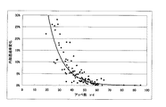
同図より明らかなように、硝材のアッベ数νが大きくなればなるほど波長405nm近傍における透過率の変動が少なくなっているのが分かる。また上記関係式(1)より明らかなように、硝材が厚いほど透過率Tは低下する。 As is clear from the figure, it can be seen that the greater the Abbe number ν of the glass material, the less the variation in transmittance near the wavelength of 405 nm. Further, as apparent from the relational expression (1), the transmittance T decreases as the glass material becomes thicker.
一般的に入射光学系LAを構成するレンズの厚みが3〜5mm程度なのに対して、結像光学系6を構成するレンズの厚みがfθ特性と像面湾曲量を良好にさせるために5〜10mm程度と比較的厚くなる。そのため結像光学系6を構成する硝材のアッベ数を大きくすることで、入射光学系LAのみの透過光量でAPC動作させて光量を一定に保っても、感光ドラム面8上の光量のバラツキに影響が少ないと考えられる。
In general, the thickness of the lens constituting the incident optical system LA is about 3 to 5 mm, whereas the thickness of the lens constituting the imaging
図8より結像光学系6を構成する各結像レンズの材質のアッベ数が40以上であれば波長変動による結像光学系6の透過率変動が少ないため望ましい。
From FIG. 8, it is preferable that the Abbe number of the material of each imaging lens constituting the imaging
そこで本実施例では下記の表−4に示すように結像光学系6を構成する屈折光学素子としての第1、第2、第3の結像レンズ6a,6b、6cに、その材質のアッベ数が各々40以上の硝材を用いることにより、上記の課題を解決している。
Therefore, in this embodiment, as shown in Table 4 below, the first, second, and
表−3に本発明の実施例1の各レンズの光学配置及び形状を示す。表―4に本実施例における各レンズの硝材名及びアッベ数を示す。 Table 3 shows the optical arrangement and shape of each lens of Example 1 of the present invention. Table 4 shows the glass material name and Abbe number of each lens in this example.
本実施例では実施例1に比して第1の結像レンズ6aおよび第2の結像レンズ6bの硝材をs-bsm14(アッベ数:60.64)およびs-bsl7(アッベ数:64.14)に変更することで、波長が1nm以上変化したときでも結像光学系6での透過率の変動を0.28%まで抑えている。これにより入射光学系LAを通過した後で光量を検知してAPC制御させても感光ドラム面8上の光量の変動は少ない。
In this embodiment, the glass materials of the
また近年、製作が容易なことと光学性能をさらに向上させるために射出成形によって非球面形状をもつ樹脂レンズを結像光学系6に使用することが多くなっている。
In recent years, a resin lens having an aspherical shape by injection molding is often used for the imaging
図9に厚みが10mmであるZEONEX 480R(アッベ数:56.2(25℃、d線))の波長に対する透過率の変動を示す。 FIG. 9 shows the variation in transmittance with respect to the wavelength of ZEONEX 480R (Abbe number: 56.2 (25 ° C., d-line)) having a thickness of 10 mm.
同図より明らかなように短波長領域において、アッベ数が小さいガラスに比べて分光透過率の変動が少なく、このような波長特性をもつ樹脂を結像レンズに選択することで感光ドラム面8上の光量を変化させないことが可能である。
As is clear from the figure, in the short wavelength region, the spectral transmittance varies less than glass having a small Abbe number, and the resin on the
図10は本発明の実施例3における光走査装置の要部斜視図である。同図において図1に示した要素と同一要素には同符番を付している。 FIG. 10 is a perspective view of an essential part of the optical scanning device according to the third embodiment of the present invention. In the figure, the same elements as those shown in FIG.
本実施例において前述の実施例2と異なる点は、光量検知の構成を簡略化するために半導体レーザー1近傍に光量検知センサー14を配置し、該光量検知センサー14の手前に補正板19を配置したことである。その他の構成及び光学的作用は実施例2と略同様であり、これにより同様な効果を得ている。
This embodiment differs from the second embodiment described above in that a light
即ち、同図において18は光分割手段としてのハーフミラーであり、半導体レーザー1と入射光学系LAとの間の光路中に設けられている。ハーフミラー18は半導体レーザー1から出射した光束を透過光と反射光の2つに分割し、透過光を感光ドラム面8へ、反射光を光量検知センサー14へ向かうようにしている。
That is, in the figure,
19は補正板であり、ハーフミラー18と光量検知センサー14との間の光路中に配されており、半導体レーザー1から放射される光束の波長変動に伴う入射光学系LAと結像光学系6の分光透過率の変動と略同一又は比例する光学特性を有している。(請求項5)
本実施例において第1のレンズ(コリメータレンズ)3は出射する平行光束の波面収差を良好にするために高屈折率材料を使うことが多く、このような硝材はアッベ数が40以下と比較的小さい。
In this embodiment, the first lens (collimator lens) 3 often uses a high refractive index material in order to improve the wavefront aberration of the emitted parallel light flux, and such a glass material has an Abbe number of 40 or less. small.
また半導体レーザー1の波長変動による感光ドラム面8におけるピント変動を抑えるために入射光学系LAで色消しできるような硝材を選択するとアッベ数が大きい材料と小さい材料の組み合わせてとなってしまう。
If a glass material that can be erased by the incident optical system LA is selected in order to suppress focus fluctuation on the
そこで本実施例では上記の如く半導体レーザー1の近傍に光量検知センサー14を配置し、APC動作を行った場合でも、入射光学系LAでの光量の損失を予測できるように上述した光学特性を有する補正板19を該光量検知センサー14の手前に配置している。これにより前述の実施例2と同様な効果を得ている。
Therefore, in this embodiment, the light
ここで半導体レーザー1の出射光量をI0(λ)、補正板19の透過率をT(λ)とすると光量検知センサー14への入射光量I(λ)は
I(λ)=T(λ)×I0(λ)・・・(2)
となる。さらに環境温度が変化して、レーザー波長がλ1に変化したとすると、
I(λ1)=T(λ1)×I0(λ1)・・・(3)
となる。ここで光量検知センサー14への入射光量I(λ)をλによらず常に一定となるようにAPC動作させると、
I(λ)=T(λ)×I0(λ)=I(λ1) =T(λ1)×I0(λ1)
∴ I0(λ1)={T(λ)/T(λ1)}×I0(λ)・・・(4)
となり、感光ドラム面8へ入射する光量は、硝材の分光透過特性を補正するかのように光量補正される。
Here, when the emitted light quantity of the
I (λ) = T (λ) × I 0 (λ) (2)
It becomes. If the ambient temperature changes and the laser wavelength changes to λ 1 ,
I (λ 1 ) = T (λ 1 ) × I 0 (λ 1 ) (3)
It becomes. Here, when the APC operation is performed so that the incident light quantity I (λ) to the light
I (λ) = T (λ) × I 0 (λ) = I (λ 1 ) = T (λ 1 ) × I 0 (λ 1 )
∴ I 0 (λ 1 ) = {T (λ) / T (λ 1 )} × I 0 (λ) (4)
Thus, the amount of light incident on the
補正板19は波長変動に対する全系の透過率変動と同一又は比例するように厚みと硝材を選択している。補正板19を配置することで半導体レーザー1の波長が変動しても、光量検知センサー14面上の光量と感光ドラム面8上の光量とが略同一になるために、APC動作を行うことで感光ドラム面8上の光量は略一定にすることができる。もし、目的とする分光透過率特性をもつ硝材が無い場合でも、誘電体多層膜により自由に設計することができるため必要とする分光透過率に合わせることが可能である。
The thickness and glass material of the
尚、本実施例では補正板19を用いたが、これに限らず、例えば光量検知センサー14の検知感度(感度特性)が波長変動に対する全系の透過率変動と同一または比例になるように設定することでも上記の実施例3と同一の効果を得ることができる。
In this embodiment, the
もしくは図11に示すように半導体レーザー1の近傍(周囲)に温度変化をリアルタイムに測定する温度センサー20を配置する。そして温度センサー20からの出力信号より、温度変化があったとき、該半導体レーザー1から放射される光束の波長変動に伴う入射光学系LAと結像光学系6の分光透過率の変動を予測手段21により予測する。そして予測手段21からの信号に基づいて、該半導体レーザー1の出力を制御手段15により制御するように構成する。このように構成することによって上記の実施例3と同様な効果を得ることができる。
Alternatively, as shown in FIG. 11, a
尚、本実施例においては単一の光源(レーザー)についてのAPC動作について述べたが、複数の光源についても同様であり、光源毎に補正板19を通過させてAPC動作を行うことで複数の光源における濃度ムラを抑えることができる。
In the present embodiment, the APC operation for a single light source (laser) has been described. The same applies to a plurality of light sources, and a plurality of light sources are passed through the
図12は本発明の実施例4における光走査装置の要部概略図である。同図において図1に示した要素と同一要素には同符番を付している。
FIG. 12 is a schematic diagram of a main part of an optical scanning device according to
本実施例において前述の実施例1と異なる点は、光源手段81を面発光型レーザーより構成し、かつ該光源手段81と光偏向器5との間の光路中に波長変動補正板22を設けたことである。その他の構成及び光学的作用は実施例1と略同様であり、これにより同様な効果を得ている。
The present embodiment is different from the first embodiment in that the light source means 81 is composed of a surface emitting laser, and a wavelength
即ち、同図において81は複数の発光点(発光部)を有する光源手段であり、例えば該光源手段81から発せられる複数の光束の波長が450nm以下(本実施例では405nm)である面発光型レーザー(短波長面発光レーザー)より成っている。
That is, in the figure,
22は波長変動補正板であり、光源手段81から放射される光束の波長の変動領域において、入射光学系LAと結像光学系6の分光透過率分布と逆の分光透過率分布を有する材料より成っている。
さらに波長変動補正板22は、光源手段81の複数の発光部から放射された光束間に波長差があっても各光束が被走査面に入射するときの光束間の光量差を少なくする分光透過率分布を有している。
Further, the wavelength
本実施例において、面発光型レーザー81より射出した複数の発散光束は第1のレンズ3により収束光束に変換され、開口絞り2によって所望のビーム形状に整形してシリンドリカルレンズ4に入射する。シリンドリカルレンズ4に入射した複数の光束のうち主走査断面内においてはそのままの状態で射出する。また副走査断面内においては収束して光偏向器5の偏向面5aにほぼ線像(主走査方向に長手の線像)として結像する。そして光偏向器5の偏向面5aで反射偏向された複数の光束は結像光学系6により感光ドラム面8上にスポット形状に結像され、該光偏向器5を矢印A方向に回転させることによって、感光ドラム面8上を複数の光束で矢印B方向(主走査方向)に等速度で光走査している。これにより記録媒体である感光ドラム面8上に複数の走査線を同時に形成し、画像記録を行っている。
In the present embodiment, a plurality of divergent light beams emitted from the
このとき本実施例においては感光ドラム面8上を光スポットで走査する前に該感光ドラム面8上における画像形成を開始するタイミングを調整するために、光検出器としてのBD(beam detector)センサ−10が設けられている。このBDセンサー10は光偏向器5で反射偏向された光束の一部であるBD光束、即ち感光ドラム面8上の画像形成領域を走査する前の画像形成領域外の領域を走査している時の光束を受光する。このBD光束はBDミラー13で反射され、BDレンズ(不図示)で集光されてBDセンサー10に入射する。そしてこのBDセンサー10の出力信号からBD信号(同期信号)を検出し、このBD信号に基づいて感光ドラム面8における画像記録の開始タイミングを調整している。
At this time, in this embodiment, a BD (beam detector) sensor as a photodetector is used to adjust the timing of starting image formation on the
ここで、複数の発光点を個別に発光させて個々に光量を検知し、APC動作を行うと多大な時間がかかる恐れがあるので、一般的には複数の発光点のうち1点ないし数点をピックアップして光量を検知している。ただし、面発光型レーザー81において個々の発光点に波長ばらつきが発生した場合、硝材の透過率が波長によって異なるために、感光ドラム面8上の光量が各発光点で異なる恐れがある。
Here, if a plurality of light emitting points are individually emitted to individually detect the amount of light and perform an APC operation, it may take a lot of time. Is picked up to detect the amount of light. However, in the surface-emitting
そこで本実施例では図12に示すようにシリンドリカルレンズ4と光偏向器5との間の光路中に波長変動補正板22を設けることによって上記の問題点を解決している。この波長変動補正板22は上記の如く面発光型レーザー81から放射される光束の波長の変動領域において、入射光学系LAと結像光学系6の分光透過率分布と逆の分光透過率分布を有する材料より成っている。かつ面発光型レーザー81の複数の発光部から放射された光束間に波長差があっても各光束が被走査面に入射するときの光束間の光量差を少なくする分光透過率分布を有している。
Therefore, in this embodiment, the above-described problem is solved by providing a wavelength
図13に本実施例の波長変動補正板22の透過率特性を示す。また表−5に本実施例における波長変動補正板22における誘電体多層膜の膜材料と膜厚を示す。
FIG. 13 shows the transmittance characteristics of the wavelength
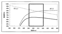
波長変動補正板22の分光透過率分布T’(λ)はすべての硝材を透過した後の分光透過率分布をA(λ)としたとき、各発光点の波長がばらつく範囲(図中の枠内で囲った領域)において太実線に示されるように、
T’(λ)=const./A(λ)・・・(5)
となる特性をもつ。したがって面発光型レーザー81の波長バラツキがあったとしても、波長変動補正板22を透過することで感光ドラム面8上の光量は略一定にすることができる。誘電体多層膜により自由に設計することができるため関係式(5)を満足できる分光透過率に合わせることが可能である。
The spectral transmittance distribution T ′ (λ) of the wavelength
T '(λ) = const. / A (λ) (5)
It has the characteristic that becomes. Therefore, even if there is a wavelength variation of the
本実施例では面発光型レーザーについて述べたが、これに限らず、例えば複数の光源(レーザー)で構成される系についても波長のばらつきに応じて波長変動補正板22の分光透過率特性を決定するようにすればよい。
In the present embodiment, the surface emitting laser is described. However, the present invention is not limited to this. For example, the spectral transmittance characteristic of the wavelength
[画像形成装置]
図14は本発明の画像形成装置の実施例を示す副走査方向の要部断面図である。図において、符号104は画像形成装置を示す。この画像形成装置104には、パーソナルコンピュータ等の外部機器117からコードデータDcが入力する。このコードデータDcは、装置内のプリンタコントローラ111によって、画像データ(ドットデータ)Diに変換される。この画像データDiは、実施例1〜4のいずれかに示した構成を有する光走査ユニット100に入力される。そして、この光走査ユニット100からは、画像データDiに応じて変調された光ビーム103が出射され、この光ビーム103によって感光ドラム101の感光面が主走査方向に走査される。
[Image forming apparatus]
FIG. 14 is a cross-sectional view of an essential part in the sub-scanning direction showing an embodiment of the image forming apparatus of the present invention. In the figure,
静電潜像担持体(感光体)たる感光ドラム101は、モータ115によって時計廻りに回転させられる。そして、この回転に伴って、感光ドラム101の感光面が光ビーム103に対して、主走査方向と直交する副走査方向に移動する。感光ドラム101の上方には、感光ドラム101の表面を一様に帯電せしめる帯電ローラ102が表面に当接するように設けられている。そして、帯電ローラ102によって帯電された感光ドラム101の表面に、前記光走査ユニット100によって走査される光ビーム103が照射されるようになっている。
The
先に説明したように、光ビーム103は、画像データDiに基づいて変調されており、この光ビーム103を照射することによって感光ドラム101の表面に静電潜像を形成せしめる。この静電潜像は、上記光ビーム103の照射位置よりもさらに感光ドラム101の回転方向の下流側で感光ドラム101に当接するように配設された現像器107によってトナー像として現像される。
As described above, the
現像器107によって現像されたトナー像は、感光ドラム101の下方で、感光ドラム101に対向するように配設された転写ローラ108によって被転写材たる用紙112上に転写される。用紙112は感光ドラム101の前方(図14において右側)の用紙カセット109内に収納されているが、手差しでも給紙が可能である。用紙カセット109端部には、給紙ローラ110が配設されており、用紙カセット109内の用紙112を搬送路へ送り込む。
The toner image developed by the developing
以上のようにして、未定着トナー像を転写された用紙112はさらに感光ドラム101後方(図14において左側)の定着器へと搬送される。定着器は内部に定着ヒータ(図示せず)を有する定着ローラ113とこの定着ローラ113に圧接するように配設された加圧ローラ114とで構成されており、転写部から搬送されてきた用紙112を定着ローラ113と加圧ローラ114の圧接部にて加圧しながら加熱することにより用紙112上の未定着トナー像を定着せしめる。更に定着ローラ113の後方には排紙ローラ116が配設されており、定着された用紙112を画像形成装置の外に排出せしめる。
As described above, the
図14においては図示していないが、プリントコントローラ111は、先に説明したデータの変換だけでなく、モータ115を始め画像形成装置内の各部や、後述する光走査ユニット内のポリゴンモータなどの制御を行う。
Although not shown in FIG. 14, the
本発明で使用される画像形成装置の記録密度は、特に限定されない。しかし、記録密度が高くなればなるほど、高画質が求められることを考えると、1200dpi以上の画像形成装置において本発明の実施例1〜4の構成はより効果を発揮する。 The recording density of the image forming apparatus used in the present invention is not particularly limited. However, considering that the higher the recording density is, the higher the image quality is required, the configurations of the first to fourth embodiments of the present invention are more effective in an image forming apparatus of 1200 dpi or more.
[カラー画像形成装置]
図15は本発明の実施例のカラー画像形成装置の要部概略図である。本実施例は、光走査装置を4個並べ各々並行して像担持体である感光ドラム面上に画像情報を記録するタンデムタイプのカラー画像形成装置である。図15において、60はカラー画像形成装置、61,62,63,64は各々実施例1〜4に示したいずれかの構成を有する光走査装置、21,22,23,24は各々像担持体としての感光ドラム、31,32,33,34は各々現像器、51は搬送ベルトである。
[Color image forming apparatus]
FIG. 15 is a schematic view of a main part of a color image forming apparatus according to an embodiment of the present invention. This embodiment is a tandem type color image forming apparatus in which four optical scanning devices are arranged in parallel and image information is recorded on a photosensitive drum surface as an image carrier. In FIG. 15, 60 is a color image forming apparatus, 61, 62, 63, and 64 are optical scanning devices each having one of the configurations shown in
図15において、カラー画像形成装置60には、パーソナルコンピュータ等の外部機器52からR(レッド)、G(グリーン)、B(ブルー)の各色信号が入力する。これらの色信号は、装置内のプリンタコントローラ53によって、C(シアン),M(マゼンタ),Y(イエロー)、B(ブラック)の各画像データ(ドットデータ)に変換される。これらの画像データは、それぞれ光走査装置61,62,63,64に入力される。そして、これらの光走査装置からは、各画像データに応じて変調された光ビーム41,42,43,44が出射され、これらの光ビームによって感光ドラム21,22,23,24の感光面が主走査方向に走査される。
In FIG. 15, the color
本実施例におけるカラー画像形成装置は光走査装置(61,62,63,64)を4個並べ、各々がC(シアン),M(マゼンタ),Y(イエロー)、B(ブラック)の各色に対応し、各々平行して感光ドラム21,22,23,24面上に画像信号(画像情報)を記録し、カラー画像を高速に印字するものである。
The color image forming apparatus in this embodiment has four optical scanning devices (61, 62, 63, 64) arranged in each color of C (cyan), M (magenta), Y (yellow), and B (black). Correspondingly, image signals (image information) are recorded on the
本実施例におけるカラー画像形成装置は上述の如く4つの光走査装置61,62,63,64により各々の画像データに基づいた光ビームを用いて各色の潜像を各々対応する感光ドラム21,22,23,24面上に形成している。その後、記録材に多重転写して1枚のフルカラー画像を形成している。
As described above, the color image forming apparatus in this embodiment uses the light beams based on the respective image data by the four
前記外部機器52としては、例えばCCDセンサを備えたカラー画像読取装置が用いられても良い。この場合には、このカラー画像読取装置と、カラー画像形成装置60とで、カラーデジタル複写機が構成される。
As the
1 光源手段(短波長レーザー)
2 開口絞り
3 第1のレンズ(コリメータレンズ)
4 レンズ系(シリンドリカルレンズ)
5 偏向手段(ポリゴンミラー)
6 結像光学系
6a,6b 結像レンズ
7 第2のレンズ(球面レンズ)
8 被走査面(感光体ドラム)
LA 第1の光学系(入射光学系)
10 BDセンサー
13 BDミラー
14 光量検知手段
15 制御手段
16 半導体レーザ駆動部
17 画像処理部
18 光分割手段
19 補正板
20 温度センサー
21 予測手段
81 光源手段(面発光型レーザー)
61、62、63、64 光走査装置
71、72、73、74 像担持体(感光ドラム)
31、32、33、34 現像器
41、42、43、44 光束
51 搬送ベルト
52 外部機器
53 プリンタコントローラ
60 カラー画像形成装置
100 光走査装置
101 感光ドラム
102 帯電ローラ
103 光ビーム
104 画像形成装置
107 現像装置
108 転写ローラ
109 用紙カセット
110 給紙ローラ
111 プリンタコントローラ
112 転写材(用紙)
113 定着ローラ
114 加圧ローラ
115 モータ
116 排紙ローラ
117 外部機器
1 Light source means (short wavelength laser)
2 Aperture stop 3 First lens (collimator lens)
4 Lens system (cylindrical lens)
5 Deflection means (polygon mirror)
6 Imaging
8 Scanned surface (photosensitive drum)
LA first optical system (incident optical system)
DESCRIPTION OF
61, 62, 63, 64 Optical scanning device 71, 72, 73, 74 Image carrier (photosensitive drum)
31, 32, 33, 34
113
Claims (8)
前記光源手段から出射された光束の波長変動に伴う前記入射光学系と前記結像光学系の分光透過率の変動を検出する光量検知手段と、
前記光量検知手段で検知された検出値に基づいて前記光源手段の出力を制御する制御手段と、を有し、
前記光量検知手段は、前記被走査面と共役の位置に配置され、前記光量検知手段は、前記入射光学系及び前記偏向手段及び前記結像光学系を通過した光束を検知しており、
前記制御手段は、温度変化があったとき、前記光源手段の出力を変化させることを特徴とする光走査装置。 Light source means for wavelength emits less light flux 450 nm, an incident optical system to be incident on deflecting means for deflecting and scanning the light beam emitted from said light source means, a surface to be scanned deflects a light beam scanned by the deflecting surface of said deflecting means In an optical scanning device comprising an imaging optical system that forms an image on the top ,
A light amount detecting means for detecting a change in spectral transmittance of the incident optical system and the imaging optical system accompanying a wavelength fluctuation of a light beam emitted from the light source means;
Control means for controlling the output of the light source means based on the detection value detected by the light quantity detection means,
The light amount detecting means is disposed at a position conjugate with the surface to be scanned, and the light amount detecting means detects a light beam that has passed through the incident optical system, the deflecting means, and the imaging optical system,
The optical scanning device characterized in that the control means changes the output of the light source means when there is a temperature change.
前記結像光学系を構成する屈折光学素子はアッベ数が40以上の材料より成り、
前記光源手段から出射された光束の波長変動に伴う前記入射光学系の分光透過率の変動を検出する光量検知手段と、
前記光量検知手段で検知された検出値に基づいて前記光源手段の出力を制御する制御手段と、を有し、
前記光量検知手段は、前記入射光学系及び前記偏向手段を通過した光束を検知しており、
前記制御手段は、温度変化があったとき、前記光源手段の出力を変化させることを特徴とする光走査装置。 Light source means for wavelength emits less light flux 450 nm, an incident optical system to be incident on deflecting means for deflecting and scanning the light beam emitted from said light source means, a surface to be scanned deflects a light beam scanned by the deflecting surface of said deflecting means In an optical scanning device comprising an imaging optical system that forms an image on the top ,
The refractive optical element constituting the imaging optical system is made of a material having an Abbe number of 40 or more,
A light amount detecting means for detecting a change in spectral transmittance of the incident optical system accompanying a wavelength fluctuation of a light beam emitted from the light source means;
Control means for controlling the output of the light source means based on the detection value detected by the light quantity detection means,
The light amount detection means detects a light beam that has passed through the incident optical system and the deflection means,
The optical scanning device characterized in that the control means changes the output of the light source means when there is a temperature change.
前記光源手段から出射した光束の一部を分割する光分割手段と、前記光分割手段で分割された光束を検出する光量検知手段と、前記光分割手段と前記光量検知手段との間に配置した補正板と、を有し、
前記補正板は、前記光源手段から出射された光束の波長変動に伴う前記入射光学系と前記結像光学系の分光透過率の変動と同一又は比例する光学特性を有しており、
温度変化があったとき、前記光量検知手段で検知された検出値に基づいて、前記光源手段の出力を変化させる制御手段を有することを特徴とする光走査装置。 A light source unit that emits a light beam having a wavelength of 450 nm or less; an incident optical system that causes the light beam emitted from the light source unit to enter a deflecting unit that deflects and scans; and a light beam deflected and scanned by the deflection surface of the deflecting unit. In an optical scanning device comprising an imaging optical system that forms an image on the top ,
Light splitting means for splitting a part of the light beam emitted from the light source means, light quantity detection means for detecting the light flux split by the light splitting means, and disposed between the light splitting means and the light quantity detection means A correction plate,
The correction plate has an optical characteristic that is the same as or proportional to a change in spectral transmittance of the incident optical system and the imaging optical system due to a change in wavelength of the light beam emitted from the light source means,
An optical scanning apparatus comprising: a control unit configured to change an output of the light source unit based on a detection value detected by the light amount detection unit when a temperature change occurs.
前記光源手段から出射した光束の一部を分割する光分割手段と、前記光分割手段で分割された光束を検出する光量検知手段と、を有し、
前記光量検知手段は、前記光源手段から出射された光束の波長変動に伴う前記入射光学系と前記結像光学系の分光透過率の変動と同一又は比例する感度特性を有しており、
温度変化があったとき、前記光量検知手段で検知された検出値に基づいて、前記光源手段の出力を変化させる制御手段を有することを特徴とする光走査装置。 Light source means for wavelength emits less light flux 450 nm, an incident optical system to be incident on deflecting means for deflecting and scanning the light beam emitted from said light source means, a surface to be scanned deflects a light beam scanned by the deflecting surface of said deflecting means In an optical scanning device comprising an imaging optical system that forms an image on the top ,
A light splitting unit that splits a part of the light beam emitted from the light source unit, and a light amount detection unit that detects the light beam split by the light splitting unit,
The light amount detection means has a sensitivity characteristic that is the same as or proportional to the change in spectral transmittance of the incident optical system and the imaging optical system accompanying the wavelength fluctuation of the light beam emitted from the light source means,
An optical scanning apparatus comprising: a control unit configured to change an output of the light source unit based on a detection value detected by the light amount detection unit when a temperature change occurs.
前記光源手段と前記偏向手段との間の光路中に波長変動補正板を有し、
前記波長変動補正板は、前記光源手段から出射された光束の波長の変動領域において、前記入射光学系と前記結像光学系の分光透過率分布と逆の分光透過率分布を有する材料より成り、かつ、
前記波長変動補正板は、前記光源手段の複数の発光部から放射された光束間に波長差があるとき各光束が前記被走査面に入射するときの光束間の光量差を少なくする分光透過率分布を有していることを特徴とする光走査装置。 A light source unit having a plurality of light emitting units for emitting a light beam having a wavelength of 450 nm or less, an incident optical system for causing the plurality of light beams emitted from the plurality of light emitting units to enter a deflecting unit for deflecting scanning, and a deflection surface of the deflecting unit In an optical scanning device comprising an imaging optical system that forms an image on a surface to be scanned with a plurality of light beams deflected and scanned in
Having a wavelength fluctuation correction plate in the optical path between the light source means and the deflection means;
The wavelength variation correction plate is made of a material having a spectral transmittance distribution opposite to the spectral transmittance distribution of the incident optical system and the imaging optical system in the wavelength variation region of the light beam emitted from the light source means , And,
The wavelength fluctuation correction plate reduces the light amount difference between the light beams when each light beam is incident on the scanned surface when there is a wavelength difference between the light beams emitted from the plurality of light emitting units of the light source means. An optical scanning device having a distribution .
前記光源手段の周囲に、温度を検出する温度センサーと、前記温度センサーからの出力信号に基づいて前記光源手段から出射された光束の波長変動に伴う前記入射光学系と前記結像光学系の分光透過率の変動を予測する予測手段と、
前記予測手段からの信号に基づいて、前記光源手段の出力を変化させる制御手段を有することを特徴とする光走査装置。 Light source means for wavelength emits less light flux 450 nm, an incident optical system to be incident on deflecting means for deflecting and scanning the light beam emitted from said light source means, a plurality of light beam scanningly deflected by the deflecting surface of said deflecting means to be In an optical scanning device comprising an imaging optical system that forms an image on a scanning surface ,
A temperature sensor for detecting a temperature around the light source means, and a spectrum of the incident optical system and the imaging optical system according to a wavelength variation of a light beam emitted from the light source means based on an output signal from the temperature sensor A prediction means for predicting the variation in transmittance;
An optical scanning apparatus comprising control means for changing the output of the light source means based on a signal from the prediction means.
Priority Applications (2)
| Application Number | Priority Date | Filing Date | Title |
|---|---|---|---|
| JP2005280432A JP4641478B2 (en) | 2005-09-27 | 2005-09-27 | Optical scanning device and image forming apparatus using the same |
| US11/533,854 US7542189B2 (en) | 2005-09-27 | 2006-09-21 | Light scanning apparatus and image forming apparatus using the light scanning apparatus |
Applications Claiming Priority (1)
| Application Number | Priority Date | Filing Date | Title |
|---|---|---|---|
| JP2005280432A JP4641478B2 (en) | 2005-09-27 | 2005-09-27 | Optical scanning device and image forming apparatus using the same |
Publications (3)
| Publication Number | Publication Date |
|---|---|
| JP2007093774A JP2007093774A (en) | 2007-04-12 |
| JP2007093774A5 JP2007093774A5 (en) | 2008-11-13 |
| JP4641478B2 true JP4641478B2 (en) | 2011-03-02 |
Family
ID=37910846
Family Applications (1)
| Application Number | Title | Priority Date | Filing Date |
|---|---|---|---|
| JP2005280432A Expired - Fee Related JP4641478B2 (en) | 2005-09-27 | 2005-09-27 | Optical scanning device and image forming apparatus using the same |
Country Status (2)
| Country | Link |
|---|---|
| US (1) | US7542189B2 (en) |
| JP (1) | JP4641478B2 (en) |
Families Citing this family (15)
| Publication number | Priority date | Publication date | Assignee | Title |
|---|---|---|---|---|
| US7944599B2 (en) | 2004-09-27 | 2011-05-17 | Qualcomm Mems Technologies, Inc. | Electromechanical device with optical function separated from mechanical and electrical function |
| US7916980B2 (en) * | 2006-01-13 | 2011-03-29 | Qualcomm Mems Technologies, Inc. | Interconnect structure for MEMS device |
| US7471442B2 (en) * | 2006-06-15 | 2008-12-30 | Qualcomm Mems Technologies, Inc. | Method and apparatus for low range bit depth enhancements for MEMS display architectures |
| US7924487B2 (en) * | 2007-02-09 | 2011-04-12 | Ricoh Company, Ltd. | Optical scanning device and image forming apparatus |
| JP5034722B2 (en) * | 2007-07-05 | 2012-09-26 | コニカミノルタアドバンストレイヤー株式会社 | Scanning optical system, optical scanning device, and image forming apparatus |
| JP5006810B2 (en) | 2008-02-06 | 2012-08-22 | 株式会社リコー | Optical scanning apparatus and image forming apparatus |
| US7944604B2 (en) | 2008-03-07 | 2011-05-17 | Qualcomm Mems Technologies, Inc. | Interferometric modulator in transmission mode |
| US7859740B2 (en) | 2008-07-11 | 2010-12-28 | Qualcomm Mems Technologies, Inc. | Stiction mitigation with integrated mech micro-cantilevers through vertical stress gradient control |
| JP5428666B2 (en) * | 2008-09-17 | 2014-02-26 | 株式会社リコー | Image forming apparatus and image forming method |
| JP2010214599A (en) * | 2009-03-13 | 2010-09-30 | Ricoh Co Ltd | Optical scanning apparatus and image forming apparatus |
| US8736939B2 (en) | 2011-11-04 | 2014-05-27 | Qualcomm Mems Technologies, Inc. | Matching layer thin-films for an electromechanical systems reflective display device |
| US9910259B2 (en) | 2013-07-09 | 2018-03-06 | Corey Zieger | Modular holographic sighting system |
| US9500442B2 (en) | 2013-07-15 | 2016-11-22 | OptiFlow, Inc. | Holographic gun sight |
| US10247515B2 (en) | 2015-06-26 | 2019-04-02 | Ziel Optics, Inc. | Holographic sight with optimized reflection and image angles |
| US10254532B2 (en) | 2015-06-26 | 2019-04-09 | Ziel Optics, Inc. | Hybrid holographic sight |
Citations (3)
| Publication number | Priority date | Publication date | Assignee | Title |
|---|---|---|---|---|
| JPH10193679A (en) * | 1997-01-08 | 1998-07-28 | Hitachi Ltd | Laser light source and laser printer |
| JP2003266759A (en) * | 2002-03-15 | 2003-09-24 | Konica Corp | Image recorder and image recording method |
| JP2004078192A (en) * | 2001-01-11 | 2004-03-11 | Canon Inc | Optical scanner and imaging apparatus using same |
Family Cites Families (3)
| Publication number | Priority date | Publication date | Assignee | Title |
|---|---|---|---|---|
| US5054866A (en) * | 1988-12-29 | 1991-10-08 | Ricoh Company, Ltd. | Scanning optical apparatus |
| JP3507474B2 (en) | 2001-01-11 | 2004-03-15 | キヤノン株式会社 | Optical scanning device and image forming apparatus using the same |
| JP4590166B2 (en) | 2003-05-27 | 2010-12-01 | キヤノン株式会社 | Optical scanning device and image forming apparatus using the same |
-
2005
- 2005-09-27 JP JP2005280432A patent/JP4641478B2/en not_active Expired - Fee Related
-
2006
- 2006-09-21 US US11/533,854 patent/US7542189B2/en not_active Expired - Fee Related
Patent Citations (3)
| Publication number | Priority date | Publication date | Assignee | Title |
|---|---|---|---|---|
| JPH10193679A (en) * | 1997-01-08 | 1998-07-28 | Hitachi Ltd | Laser light source and laser printer |
| JP2004078192A (en) * | 2001-01-11 | 2004-03-11 | Canon Inc | Optical scanner and imaging apparatus using same |
| JP2003266759A (en) * | 2002-03-15 | 2003-09-24 | Konica Corp | Image recorder and image recording method |
Also Published As
| Publication number | Publication date |
|---|---|
| JP2007093774A (en) | 2007-04-12 |
| US7542189B2 (en) | 2009-06-02 |
| US20070081213A1 (en) | 2007-04-12 |
Similar Documents
| Publication | Publication Date | Title |
|---|---|---|
| JP4641478B2 (en) | Optical scanning device and image forming apparatus using the same | |
| US7050209B2 (en) | Scanning optical apparatus and image forming apparatus using the same | |
| JP4314010B2 (en) | Optical scanning device and image forming apparatus using the same | |
| JP4819436B2 (en) | Optical scanning device and method of adjusting optical scanning device | |
| US7397590B2 (en) | Optical scanning apparatus and image forming apparatus employing this apparatus | |
| JP4677277B2 (en) | Optical scanning device and image forming apparatus using the same | |
| US8063927B2 (en) | Optical scanning apparatus and image-forming apparatus using the same | |
| JP5173879B2 (en) | Optical scanning device and image forming apparatus using the same | |
| US7526145B2 (en) | Optical scanning device and image forming apparatus using the same | |
| JP2002333585A (en) | Scanning optical device and image forming device using the same | |
| JP4455309B2 (en) | Optical scanning device and image forming apparatus using the same | |
| JP4594040B2 (en) | Optical scanning device and image forming apparatus using the same | |
| JP4630593B2 (en) | Scanning optical device and image forming apparatus using the same | |
| JP4401950B2 (en) | Optical scanning device and image forming apparatus using the same | |
| JP4401951B2 (en) | Optical scanning device and image forming apparatus using the same | |
| JP2005088352A (en) | Scanning optical device and image forming apparatus using it | |
| JP2005070125A (en) | Optical scanner and image forming apparatus using same | |
| JP6436657B2 (en) | Optical scanning apparatus and image forming apparatus | |
| JP4208750B2 (en) | Optical scanning device and image forming apparatus using the same | |
| JP2010049060A (en) | Scanning optical apparatus and image forming apparatus using the same | |
| JP2007155837A (en) | Optical scanner and image forming apparatus using the same | |
| JP2009204940A (en) | Optical scanner and image forming apparatus using the same | |
| JP2004145051A (en) | Scanning optical system and image forming apparatus using the same |
Legal Events
| Date | Code | Title | Description |
|---|---|---|---|
| A521 | Request for written amendment filed |
Free format text: JAPANESE INTERMEDIATE CODE: A523 Effective date: 20080925 |
|
| A621 | Written request for application examination |
Free format text: JAPANESE INTERMEDIATE CODE: A621 Effective date: 20080925 |
|
| TRDD | Decision of grant or rejection written | ||
| A977 | Report on retrieval |
Free format text: JAPANESE INTERMEDIATE CODE: A971007 Effective date: 20101116 |
|
| A01 | Written decision to grant a patent or to grant a registration (utility model) |
Free format text: JAPANESE INTERMEDIATE CODE: A01 Effective date: 20101124 |
|
| A01 | Written decision to grant a patent or to grant a registration (utility model) |
Free format text: JAPANESE INTERMEDIATE CODE: A01 |
|
| A61 | First payment of annual fees (during grant procedure) |
Free format text: JAPANESE INTERMEDIATE CODE: A61 Effective date: 20101129 |
|
| R150 | Certificate of patent or registration of utility model |
Ref document number: 4641478 Country of ref document: JP Free format text: JAPANESE INTERMEDIATE CODE: R150 Free format text: JAPANESE INTERMEDIATE CODE: R150 |
|
| FPAY | Renewal fee payment (event date is renewal date of database) |
Free format text: PAYMENT UNTIL: 20131210 Year of fee payment: 3 |
|
| RD03 | Notification of appointment of power of attorney |
Free format text: JAPANESE INTERMEDIATE CODE: R3D03 |
|
| LAPS | Cancellation because of no payment of annual fees |