JP4637320B2 - Goggles type display device - Google Patents
Goggles type display device Download PDFInfo
- Publication number
- JP4637320B2 JP4637320B2 JP2000142490A JP2000142490A JP4637320B2 JP 4637320 B2 JP4637320 B2 JP 4637320B2 JP 2000142490 A JP2000142490 A JP 2000142490A JP 2000142490 A JP2000142490 A JP 2000142490A JP 4637320 B2 JP4637320 B2 JP 4637320B2
- Authority
- JP
- Japan
- Prior art keywords
- liquid crystal
- display device
- crystal panel
- type display
- goggle type
- Prior art date
- Legal status (The legal status is an assumption and is not a legal conclusion. Google has not performed a legal analysis and makes no representation as to the accuracy of the status listed.)
- Expired - Fee Related
Links
Images


Landscapes
- Devices For Indicating Variable Information By Combining Individual Elements (AREA)
- Liquid Crystal (AREA)
Description
【0001】
【発明の属する技術分野】
【0002】
本明細書で開示する発明は、ゴーグル型表示装置に関する。本明細書では、ゴーグル型表示装置というが、ヘッドマウントディスプレイ(HMD)と呼ばれる場合もある。
【0003】
【従来の技術】
【0004】
近年、使用者が頭部に装着して使用するゴーグル型の表示装置が普及してきている。このゴーグル型の表示装置は、HMD(ヘッドマウントディスプレイ)とも呼ばれ、映像を拡大してその虚像を形成するレンズ、およびそのレンズの焦点距離よりも近くに設置された液晶パネルのような表示装置を有している。使用者は、液晶パネルの表示をレンズを介して観察することによって、拡大された映像を鑑賞することができる。よって、小型でありながらも、大画面の表示を鑑賞することができる。
【0005】
図45を参照する。11802の液晶パネルに表示された画像は11801のレンズの中を通り、11803の使用者の眼球内の網膜上に投影される。このとき11802の液晶パネルには11805Aおよび11805Bの偏光板をはり、光源として面内が均一に光る11804のバックライトを使用する必要がある。
【0006】
また移動中の使用を可能とするゴーグル型表示装置は、安全のためディスプレイと顔の隙間から外を見ることが可能である。
【0007】
【発明が解決しようとする課題】
【0008】
このゴーグル型表示装置は、上述したように使用者が頭部に装着して使用するため、据え置き型の表示装置と比較して本体の対衝撃性が高いことが求められる。かつ、ゴーグル型表示装置は、使用中常に動いていることになり、内部の光学系が置き型の表示装置と比較して、「ずれ」を生じ易い。
【0009】
ゴーグル型表示装置は、液晶パネルの表示をレンズを介して観察するので、液晶パネルとレンズとの「ずれ」が表示品質の劣化に直接つながってしまうという問題があった。
【0010】
このゴーグル型用表示装置は使用者が頭部に装着して使用することから小型化、軽量化が求められている。また携帯して使用することからいっそうの低消費電力化が必要とされている。
【0011】
そこで、本願発明は上述の問題を鑑みてなされたものであり、上述の問題を解決するゴーグル型表示装置を提供することを課題とする。
【0012】
【課題を解決するための手段】
【0013】
本発明は、上述の課題を解決するために次のような手段を採った。図1を参照する。図1には、本発明のゴーグル型表示装置に用いられる光学素子であるレンズと画像表示部品である液晶パネルおよびバックライトとが示されている。本発明によると、液晶パネルがレンズに固定されており、液晶パネルとレンズとの相対位置がずれることはない。
【0014】
図1において、101はレンズ、102は液晶パネル、103はバックライト、104は使用者の眼球である。レンズ101には、あらかじめ液晶パネルが固定される溝がもうけられており、その溝に液晶パネル102が組み込まれている。
【0015】
なお、バックライト103は、液晶パネルまたはレンズに固定されていても良い。
【0016】
上述のように、本発明によると、画像の表示を行う液晶パネルと、その画像を拡大し使用者の眼球に投射する光学素子(レンズ)との相対位置の経時変化がおこらない。よって、液晶パネルとレンズとの相対位置に関してはメンテナンスフリーである。
【0017】
本発明は、上述の課題を解決するために次のような手段を採った。本発明のゴーグル型表示装置は、音声再生装置と、表示装置である自発光型のELパネルと、表示された映像を拡大して眼に導くためプリズム、レンズ、ミラーなどで構成された光学素子と、音声再生装置と表示装置とを制御するための駆動装置とで構成される。ELパネルは有機ELディスプレイ(OELD:Organic EL Display)又は有機ライトエミッティングダイオード(OLED:Organic Light Emitting Diode)とも呼ばれている。自発光型のELパネルを使用することにより、液晶パネルと異なりバックライトを使用することなく、使用者に高輝度の映像を提供することが出来る。またバックライトを使用しないので、低消費電力化をはかることが出来る。
【0018】
また液晶パネルを使用する場合、光学素子、液晶パネル、バックライトの三者の相対位置がずれない様に固定する器具が必要である。ELパネルを使用する場合、光学素子とELパネルの二者がずれない様に固定するだけなので、ずれが生じにくく、しかも液晶パネルを使用するよりも、バックライト分の重量を減らせ、固定基材の軽量化をはかることが出来る。
【0019】
さらにELパネルでは液晶パネルと異なり偏光板を使用する必要がないため、偏光板を使用することによる輝度の低下が生じない。
【0020】
なお、音声再生装置は有していなくともよい。
【0021】
本発明によると、
表示装置と、
光学素子と、
を有するゴーグル型表示装置であって、
前記表示装置および前記光学素子は、一体となっていることを特徴とするゴーグル型表示装置が提供される。
【0022】
本発明によると、
表示装置と、
前記表示装置によって表示される映像を拡大するレンズと、
を有するゴーグル型表示装置であって、
前記表示装置および前記レンズは、一体となっていることを特徴とするゴーグル型表示装置が提供される。
【0023】
本発明によると、
表示装置と、
前記表示装置によって表示される映像を拡大するレンズと、
を有するゴーグル型表示装置であって、
前記表示装置は、前記レンズの一部に組み込まれていることを特徴とするゴーグル型表示装置が提供される。
【0024】
本発明によると、
表示装置と、
光学素子と、
を有するゴーグル型表示装置であって、
前記表示装置および前記光学素子は、一体形成されていることを特徴とするゴーグル型表示装置が提供される。
【0025】
本発明によると、
表示装置と、
前記表示装置によって表示される映像を拡大するレンズと、
を有するゴーグル型表示装置であって、
前記表示装置および前記レンズは、一体形成されていることを特徴とするゴーグル型表示装置が提供される。
【0026】
本発明によると、
前記表示装置は外部から電波によって信号を受信し、前記信号を整流化することによって前記表示装置の電源とすることを特徴とする請求項1乃至6のいずれか一に記載のゴーグル型表示装置が提供される。
【0027】
本発明によると、
前記表示装置は液晶パネルであり、前記液晶パネルに用いられる液晶材料は、実質的にしきい値を有しない反強誘電性液晶であることを特徴とする請求項1乃至7のいずれか一に記載の液晶パネルが提供される。
【0028】
本発明によると、
前記液晶材料は、V字型の電気光学特性を有する反強誘電性混合液晶であることを特徴とする請求項8に記載の液晶パネルが提供される。
【0029】
本発明によると、
前記液晶パネルの画素部の対角サイズが2インチ以下であり、前記液晶パネルの画素TFTのチャネル幅が0.2μm以上2μm以下であり、かつ前記画素TFTの活性層膜厚が10nm〜50nmである請求項7乃至9のいずれか一に記載の液晶パネルが提供される。
【0030】
前記構成において、
前記画素TFTのチャネル幅が0.2μm以上1.3μm以下であることが提供される。
【0031】
本発明によると、
映像信号を入力し、映像を表示する表示装置と、
光学素子と、
を有するゴーグル型表示装置であって、
前記表示装置はEL素子によって構成されていることを特徴とするゴーグル型表示装置が提供される。
【0032】
本発明によると、
映像信号を入力し、映像を表示する表示装置と、
前記表示装置によって表示される映像を拡大するレンズと、
を有するゴーグル型表示装置であって、
前記表示装置はEL素子によって構成されていることを特徴とするゴーグル型表示装置が提供される。
【0033】
本発明によると、
映像信号を入力し、映像を表示する表示装置2組と、
光学素子2組と、
を有する両眼用ゴーグル型表示装置であって、
前記表示装置はEL素子によって構成されていることを特徴とするゴーグル型表示装置が提供される。
【0034】
本発明によると、
映像信号を入力し、映像を表示する表示装置2組と、
前記表示装置によって表示される映像を拡大するレンズ2組と、
を有する両眼用ゴーグル型表示装置であって、
前記表示装置はEL素子によって構成されていることを特徴とするゴーグル型表示装置が提供される。
【0035】
本発明によると、
映像信号を入力し、映像を表示する表示装置1組と、
光学素子1組と、
を有する片目用ゴーグル型表示装置であって、
前記表示装置はEL素子によって構成されていることを特徴とするゴーグル型表示装置が提供される。
【0036】
本発明によると、
映像信号を入力し、映像を表示する表示装置1組と、
前記表示装置によって表示される映像を拡大するレンズ1組と、
を有する片目用ゴーグル型表示装置であって、
前記表示装置はEL素子によって構成されていることを特徴とするゴーグル型表示装置が提供される。
【0037】
本発明によると、
映像信号を入力し、映像を表示する表示装置2組と、
前記表示装置によって表示される映像を拡大し、
かつ前方の光景を透過するレンズ2組と、
を有する両眼用ゴーグル型表示装置であって、
前記表示装置はEL素子によって構成されていることを特徴とするゴーグル型表示装置が提供される。
【0038】
【発明の実施の形態】
【0039】
以下に、本発明のゴーグル型表示装置を実施例をもって詳細に説明する。なお、本発明のゴーグル型表示装置は、以下の実施例に限定されるわけではない。
【0040】
(実施例1)
【0041】
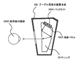
図2を参照する。図2には、本実施例のゴーグル型表示装置の概略構成図が示されている。200はゴーグル型表示装置本体、201Rおよび201Lはレンズ、202Rおよび202Lは液晶パネル、203Rおよび203Lはバックライトである。
【0042】
図3には、本実施例のゴーグル型表示装置の図2におけるA部の断面図である。図2および図3に示される様に、本実施例においては、レンズ201Rの溝に液晶パネル202Rが組み込まれている。なお、図3には、図示していないが、液晶パネル202Rは一対または一枚の偏光板が設けられるようにしても良い。なお、液晶パネル202Rと偏光板とをまとめて液晶パネルと呼ぶこともある。
【0043】
なお、液晶パネル202Rはレンズ201Rの溝に組み込まれている。
【0044】
ここで図4を参照し、本実施例の液晶パネル202Rの概略について説明する。なお、液晶パネル202Lも液晶パネル202Rと同様の構造である。
【0045】
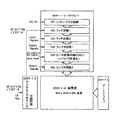
202Rはデジタルドライバを有する液晶パネルである。液晶パネル202Rは、アクティブマトリクス基板202R−1および対向基板202R−2(図示せず)を有している。アクティブマトリクス基板202R−1は、ソースドライバ202R−1−1、ゲートドライバ202R−1−2、デジタルビデオデータ分割回路202R−1−3および複数の画素TFTがマトリクス状に配置された画素部202R−1−4を有している。ソースドライバ202R−1−1およびゲートドライバ202R−1−2は画素部の複数の画素TFTを駆動する。また、対向基板202R−2は対向電極202R−2−1(図示せず)を有している。202R−1−5および202R−1−6は、FPC端子であり、これらのFPC端子に外部から種々の信号が入力される。
【0046】
次に図5を参照する。図5は本実施例の液晶パネルのソースドライバを特に詳細に示した概略構成図である。202R−1−1はソースドライバである。202R−1−2はゲートドライバである。202R−1−4は画素部である。202R−1−3はデジタルビデオデータ分割回路である。
【0047】
ソースドライバ202R−1−1は、シフトレジスタ回路(240ステージ×2のシフトレジスタ回路)501、ラッチ回路1(960×8デジタルラッチ回路)502、ラッチ回路2(960×8デジタルラッチ回路)503、セレクタ回路1(240のセレクタ回路)504、D/A変換回路(240のDAC)505、セレクタ回路2(240のセレクタ回路)506を有している。その他、バッファ回路やレベルシフタ回路(いずれも図示せず)を有している。また、説明の便宜上、D/A変換回路505にはレベルシフタ回路が含まれている。
【0048】
202R−1−2はゲートドライバであり、シフトレジスタ回路、バッファ回路、レベルシフタ回路等(いずれも図示せず)を有している。
【0049】
画素部202R−1−4は、(640×RGB)×1080(横×縦)の画素を有している。各画素には画素TFTが配置されており、各画素TFTのソース領域にはソース信号線が、ゲート電極にはゲート信号線が電気的に接続されている。また、各画素TFTのドレイン領域には画素電極が電気的に接続されている。各画素TFTは、各画素TFTに電気的に接続された画素電極への画像信号(階調電圧)の供給を制御している。各画素電極に画像信号(階調電圧)が供給され、各画素電極と対向電極との間に挟まれた液晶に電圧が印加され液晶が駆動される。
【0050】
ここで、本実施例のアクティブマトリクス型液晶パネルの動作および信号の流れを説明する。
【0051】
まず、ソースドライバの動作を説明する。シフトレジスタ回路501にクロック信号(CK)およびスタートパルス(SP)が入力される。シフトレジスタ回路501は、これらのクロック信号(CK)およびスタートパルス(SP)に基づきタイミング信号を順に発生させ、バッファ回路等(図示せず)を通して後段の回路へタイミング信号を順次供給する。
【0052】
シフトレジスタ回路501からのタイミング信号は、バッファ回路等によってバッファされる。タイミング信号が供給されるソース信号線には、多くの回路あるいは素子が接続されているために負荷容量(寄生容量)が大きい。この負荷容量が大きいために生ずるタイミング信号の立ち上がりの”鈍り”を防ぐために、このバッファ回路が設けられる。
【0053】
バッファ回路によってバッファされたタイミング信号は、ラッチ回路1(502)に供給される。ラッチ回路1(502)は、8ビットデジタルビデオデータを処理するラッチ回路を960ステージ有してる。ラッチ回路1(502)は、前記タイミング信号が入力されると、デジタルビデオデータ分割回路202R−1−3から供給される8ビットデジタルビデオデータを順次取り込み、保持する。
【0054】
ラッチ回路1(502)の全てのステージのラッチ回路にデジタルビデオデータの書き込みが一通り終了するまでの時間は、ライン期間と呼ばれる。すなわち、ラッチ回路1(502)の中で一番左側のステージのラッチ回路にデジタルビデオデータの書き込みが開始される時点から、一番右側のステージのラッチ回路にデジタルビデオデータの書き込みが終了する時点までの時間間隔がライン期間である。実際には、上記ライン期間に水平帰線期間が加えられた期間をライン期間と呼ぶこともある。
【0055】
1ライン期間の終了後、シフトレジスタ回路501の動作タイミングに合わせて、ラッチ回路2(503)にラッチシグナル(Latch Signal)が供給される。この瞬間、ラッチ回路1(502)に書き込まれ保持されているデジタルビデオデータは、ラッチ回路2(503)に一斉に送出され、ラッチ回路2(503)の全ステージのラッチ回路に書き込まれ、保持される。
【0056】
デジタルビデオデータをラッチ回路2(503)に送出し終えたラッチ回路1(502)には、シフトレジスタ回路501からのタイミング信号に基づき、再びデジタルビデオデータ分割回路から供給されるデジタルビデオデータの書き込みが順次行われる。
【0057】
この2順目の1ライン期間中には、ラッチ回路2(503)に書き込まれ、保持されているデジタルビデオデータが、セレクタ回路1(504)によって順次選択され、D/A変換回路505に供給される。なお本実施例では、セレクタ回路1(504)においては、1つのセレクタ回路がソース信号線4本に対応している。
【0058】
なお、セレクタ回路については、本出願人による特許出願である特願平9−286098号に記載されているものを用いることもできる。
【0059】
セレクタ回路504で選択されたラッチ回路2(503)からの8ビット・デジタルビデオデータがD/A変換回路505に供給される。ここで、本実施例に用いられるD/A変換回路について図7を用いて説明する。
【0060】
図7には、本実施例のD/A変換回路の回路図が示されている。なお、本実施例のD/A変換回路は、レベルシフタ回路(L.S)505−2を有しているが、このレベルシフタ回路を省略して設計することも可能である。レベルシフタ回路においては、入力INに信号Loが入力され、入力INbに信号Hiが入力された時に、出力OUTからは高電位電源VddHIが、出力OUTbからは低電位電源Vssが出力されるようになっている。また、入力INに信号Hiが入力され、入力INbに信号Loが入力された時に、出力OUTからは高電位電源Vssが、出力OUTbからは低電位電源VddHIが出力されるようになっている。
【0061】
本実施例のD/A変換回路には、NOR回路(505−1)の一方の入力にデジタルビデオデータA0〜A7の反転データ(ここでは反転A0〜反転A7と呼ぶ)が入力されるようになっている。このNOR回路(505−1)の他方の入力には、リセットパルスA(ResA)が入力される。このリセットパルスAは、D/A変換回路のリセット期間TRに入力される。本実施例の場合、デジタルビデオデータ(反転A0〜A7)はリセット期間TR中にもNOR回路(505−1)へ入力されるが、NOR回路にリセットパルスResAが入力されている間は、NOR回路からはデジタルビデオデータが出力されないようになっている。
【0062】
なお、NOR回路を省略し、リセット期間TRの終了後、デジタルビデオデータ(反転A0〜A7)が入力されるようにしてもよい。
【0063】
リセット期間TRの終了後、データ書き込み期間TEが始まり、8ビットのデジタルビデオデータがレベルシフタ回路によってその電圧レベルを上げられ、スイッチ回路SW0〜SW7に入力される。
【0064】
スイッチ回路SW0〜SW7は、それぞれ2個のアナログスイッチASW1およびASW2によって構成されている。ASW1の一端はDC_VIDEO_Lに、その他端はASW2の一端に接続されかつ容量に接続されている。また、各ASW2の一端はDC_VIDEO_Hに、その他端はASW2の一端に接続されかつ容量(1pF、2pF、4pF、8pF、1pF、2pF、4pF、8pF)に接続されている。各容量の一端は2つのアナログスイッチに接続されており、他端はリセットスイッチ2(Res2)に接続されている。また、リセットスイッチ1(Res1)の一端は、DC_VIDEO_Mに接続されており、他端は上位ビットに対応する容量の一端に接続されている。リセットスイッチRes1およびRes2には、リセットパルス(ResB)および反転リセットパルス(反転ResB)が入力される。
【0065】
また、上位ビットに対応する回路と下位ビットに対応する回路の接続点には、容量(1pF)が設けられている。なお、本実施例における、上述の全て容量はそれらの値に限定されるわけではない。
【0066】
D/A変換回路505は、8ビットのデジタルビデオデータを画像信号(階調電圧)に変換し、セレクタ回路2(506)によって選択されるソース信号線に順次供給される。
【0067】
ソース信号線に供給される画像信号は、ソース信号線に接続されている画素部の画素TFTのソース領域に供給される。
【0068】
ゲートドライバ202R−1−2においては、シフトレジスタ(図示せず)からのタイミング信号(走査信号)がバッファ回路(図示せず)に供給され、対応するゲート信号線(走査線)に供給される。ゲート信号線には、1ライン分の画素TFTのゲート電極が接続されており、1ライン分全ての画素TFTを同時にONにしなくてはならないので、バッファ回路には電流容量の大きなものが用いられる。
【0069】
このように、ゲートドライバからの走査信号によって対応する画素TFTのスイッチングが行われ、ソースドライバからの画像信号(階調電圧)が画素TFTに供給され、液晶分子が駆動される。
【0070】
202R−1−3はデジタルビデオデータ分割回路(SPC;Serial-to-Parallel Conversion Circuit)である。デジタルビデオデータ分割回路202R−1−3は、外部から入力されるデジタルビデオデータの周波数を1/xに落とすための回路である(xは2以上の自然数)。外部から入力されるデジタルビデオデータを分割することにより、駆動回路の動作に必要な信号の周波数も1/xに落とすことができる。
【0071】
ここで、本実施例の液晶パネルの液晶パネル202Rの回路構成、特に画素部202R−1−4の構成について、図6を用いて説明する。
【0072】
本実施例においては、画素部202R−1−4は、(640×RGB×480)個の画素を有している。それぞれの画素には、P1,1、P2,1、・・・、P479,1919等の符号が付けられている。また、それぞれの画素は、画素TFT601、保持容量603を有している。アクティブマトリクス基板と対向基板との間には液晶が挟まれており、液晶602は各画素に対応する液晶を模式的に示したものである。なお、COMはコモン電圧端子であり、対向電極および保持容量の一端に接続されている。
【0073】
本実施例の液晶パネルは、1ライン分の画素(例えば、P1,1、P1,2、・・・、およびP1,1919)を同時に駆動する、いわゆる線順次駆動を行う。言い換えると、1ライン分の全ての画素に同時に画像信号を書き込む。
【0074】
(実施例2)
【0075】
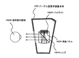
図8を参照する。図8には、本実施例のゴーグル型表示装置に用いられるレンズと画像表示部品である液晶パネルおよびバックライトとが示されている。本実施例においては、レンズの形状が実施例1と異なる。本実施例によると、液晶パネルがレンズに固定されており、液晶パネルとレンズとの相対位置がずれることはない。
【0076】
図8において、801はレンズ、802は液晶パネル、803はバックライト、804は使用者の眼球である。レンズ801には、あらかじめ液晶パネルが固定される溝がもうけられており、その溝に液晶パネル802が組み込まれている。
【0077】
なお、バックライト803は、液晶パネルまたはレンズに固定されていても良い。
【0078】
図9には、本実施例のゴーグル型表示装置の断面図が示されている。本実施例においては、レンズ801Rの溝に液晶パネル802Rが組み込まれている。なお、図9には、図示していないが、液晶パネル802Rは一対または一枚の偏光板が設けられるようにしても良い。なお、液晶パネル802Rと偏光板とをまとめて液晶パネルと呼ぶこともある。
【0079】
(実施例3)
【0080】
図10を参照する。図10には、本実施例のゴーグル型表示装置に用いられるレンズと画像表示部品である液晶パネルおよびバックライトとが示されている。本実施例においては、レンズの形状が実施例1または2と異なる。本実施例によると、液晶パネルがレンズに固定されており、液晶パネルとレンズとの相対位置がずれることはない。
【0081】
図10において、1001はレンズ、1002は液晶パネル、1003はバックライト、1004は使用者の眼球である。レンズ1001には、あらかじめ液晶パネルが固定される溝がもうけられており、その溝に液晶パネル1002が組み込まれている。
【0082】
なお、バックライト1003は、液晶パネルまたはレンズに固定されていても良い。
【0083】
図11には、本実施例のゴーグル型表示装置の断面図が示されている。本実施例においては、レンズ1001Rの溝に液晶パネル1002Rが組み込まれている。なお、図11には、図示していないが、液晶パネル1002Rは一対または一枚の偏光板が設けられるようにしても良い。なお、液晶パネル1002Rと偏光板とをまとめて液晶パネルと呼ぶこともある。
【0084】
(実施例4)
【0085】
図12を参照する。図12には、本実施例のゴーグル型表示装置に用いられるレンズと画像表示部品である液晶パネルおよびバックライトとが示されている。本実施例においては、レンズの形状が実施例1、2または3と異なる。本実施例によると、液晶パネルがレンズに固定されており、液晶パネルとレンズとの相対位置がずれることはない。
【0086】
図12において、1201はレンズ、1202は液晶パネル、1203はバックライト、1204は使用者の眼球である。レンズ1201には、あらかじめ液晶パネルが固定される溝がもうけられており、その溝に液晶パネル1202が組み込まれている。
【0087】
なお、バックライト1203は、液晶パネルまたはレンズに固定されていても良い。
【0088】
図13には、本実施例のゴーグル型表示装置の断面図が示されている。本実施例においては、レンズ1201Rの溝に液晶パネル1202Rが組み込まれている。なお、図12には、図示していないが、液晶パネル1202Rは一対または一枚の偏光板が設けられるようにしても良い。
【0089】
(実施例5)
【0090】
図14を参照する。図14には、本実施例のゴーグル型表示装置に用いられるレンズと画像表示部品である液晶パネルおよびバックライトとが示されている。本実施例においては、レンズの形状が実施例1、2、3または4と異なる。本実施例によると、液晶パネルがレンズに固定されており、液晶パネルとレンズとの相対位置がずれることはない。
【0091】
図14において、1401はレンズ、1402は液晶パネル、1403はバックライト、1404は使用者の眼球である。レンズ1401には、あらかじめ液晶パネルが固定される溝がもうけられており、その溝に液晶パネル1402が組み込まれている。
【0092】
なお、バックライト1403は、液晶パネルまたはレンズに固定されていても良い。
【0093】
図15には、本実施例のゴーグル型表示装置の断面図が示されている。本実施例においては、レンズ1401Rの溝に液晶パネル1402Rが組み込まれている。なお、図15には、図示していないが、液晶パネル1402Rは一対または一枚の偏光板が設けられるようにしても良い。
【0094】
(実施例6)
【0095】
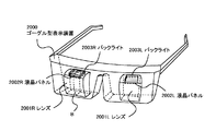
図16を参照する。図16には、本実施例のゴーグル型表示装置の概略構成図が示されている。2000はゴーグル型表示装置本体、2001Rおよび2001Lはレンズ、2002Rおよび2002Lは液晶パネル、2003Rおよび2003Lはバックライトである。
【0096】
図17には、本実施例のゴーグル型表示装置の図16におけるB部の断面図が示されている。図17に示される様に、本実施例においては、レンズ2001Rの溝と液晶パネル2002Rとが一体形成されている。図17には、レンズ2001Rの溝と液晶パネル2002Rとの境界の拡大図が示されている。つまり、レンズ2001Rの一部は、液晶パネル2002Rの対向基板として機能している。
【0097】
2001R−1は対向電極、2001R−2は配向膜であり、いずれもレンズ2001R側に形成されている。2002R−1は液晶、2002R−2は基板、2002R−4は基板上に形成された画素TFTである。2002R−3は基板上に形成された配向膜である。なお、本実施例では、対向基板側に偏光板を設けていない。用いる液晶によって一対または一枚の偏光板が設けられるようにしても良い。
【0098】
(実施例7)
【0099】
図18を参照する。図18には、本実施例のゴーグル型表示装置の概略構成図が示されている。3000はゴーグル型表示装置本体、3001Rおよび3001Lはレンズ、3002Rおよび3002Lは液晶パネル、3003Rおよび3003Lはバックライトである。3100は画像信号等の信号を電磁波として送信する信号ソースである。
【0100】
図19には、本実施例の液晶パネル3002Rおよび信号ソース3100の概略ブロック図が示されている。液晶パネル3002Rは、アクティブマトリクス基板3002R−1および対向基板3002R−2(図示せず)を有している。アクティブマトリクス基板3002R−1は、ソースドライバ3002R−1−1、ゲートドライバ3002R−1−2、デジタルビデオデータ分割回路3002R−1−3および複数の画素TFTがマトリクス状に配置された画素部3002R−1−4を有している。ソースドライバ3002R−1−1およびゲートドライバ3002R−1−2は画素部の複数の画素TFTを駆動する。また、対向基板3002R−2は対向電極3002R−2−1(図示せず)を有している。3002R−1−5および3002R−1−6は整流回路であり、それぞれコイル3002R−1−5−1、コイル3002−1−6−1によって受信した信号を整流する回路である。3002R−1−7は信号生成回路であり、整流回路3002R−1−5によって整流化された信号をもとに画像データ等の信号を生成し、3002R−1−8信号制御回路へ出力する。また、信号制御回路は、デジタルビデオデータ分割回路およびゲートドライバへ画像信号等を出力する。3002R−1−9は電圧調整回路であり電源電圧を生成する。
【0101】
信号ソースのコイル3100−1および3100−2は、信号ソースが供給する信号を電磁波として発信する。
【0102】
なお、整流回路、信号生成回路、信号制御回路は、ICチップで作成し、液晶パネルやレンズ等に固定するようにしてもよい。
【0103】
(実施例8)
【0104】
図20には、本実施例のゴーグル型表示装置のレンズ3101、液晶パネル3102、バックライト3103、マスク3104ならびに3105、使用者の眼球3106が示されている。レンズ3101には、あらかじめ液晶パネルが固定される溝がもうけられており、その溝に液晶パネル3102が組み込まれている。
【0105】
本実施例においては、マスク3104および3105が、液晶パネルの画素部以外の部分からの光を遮光する。よって、画像に関係の無い迷光を遮断することができる。
【0106】
なお、バックライト3103は、液晶パネルまたはレンズに固定されていても良い。
【0107】
図21を参照する。図21には、本実施例のゴーグル型表示装置において、上述の例と異なる位置にマスク3204および3205を配置した例である、
【0108】
(実施例9)
【0109】
ここでは画素部の画素TFTと、画素部の周辺に設けられる駆動回路(ソースドライバ、ゲートドライバ、D/A変換回路等のTFTを同一基板上に作製する方法について工程に従って詳細に説明する。但し、説明を簡単にするために、制御回路ではシフトレジスタ回路、バッファ回路、D/A変換回路などの基本回路であるCMOS回路と、nチャネル型TFTとを図示することにする。
【0110】
図22(A)において、基板6001には低アルカリガラス基板や石英基板を用いることができる。本実施例では低アルカリガラス基板を用いた。この場合、ガラス歪み点よりも10〜20℃程度低い温度であらかじめ熱処理しておいても良い。この基板6001のTFTを形成する表面には、基板6001からの不純物拡散を防ぐために、酸化シリコン膜、窒化シリコン膜または酸化窒化シリコン膜などの下地膜6002を形成する。例えば、プラズマCVD法でSiH4、NH3、N2Oから作製される酸化窒化シリコン膜を100nm、同様にSiH4、N2Oから作製される酸化窒化シリコン膜を100nmの厚さに積層形成する。
【0111】
次に、20〜150nm(好ましくは30〜80nm)の厚さで非晶質構造を有する半導体膜6003aを、プラズマCVD法やスパッタ法などの公知の方法で形成する。本実施例では、プラズマCVD法で非晶質シリコン膜を55nmの厚さに形成した。非晶質構造を有する半導体膜としては、非晶質半導体膜や微結晶半導体膜があり、非晶質シリコンゲルマニウム膜などの非晶質構造を有する化合物半導体膜を適用しても良い。また、下地膜6002と非晶質シリコン膜6003aとは同じ成膜法で形成することが可能であるので、両者を連続形成しても良い。下地膜を形成した後、一旦大気雰囲気に晒さないことでその表面の汚染を防ぐことが可能となり、作製するTFTの特性バラツキやしきい値電圧の変動を低減させることができる。(図22(A))
【0112】
そして、公知の結晶化技術を使用して非晶質シリコン膜6003aから結晶質シリコン膜6003bを形成する。例えば、レーザー結晶化法や熱結晶化法(固相成長法)を適用すれば良いが、ここでは、特開平7−130652号公報で開示された技術に従って、触媒元素を用いる結晶化法で結晶質シリコン膜6003bを形成した。結晶化の工程に先立って、非晶質シリコン膜の含有水素量にもよるが、400〜500℃で1時間程度の熱処理を行い、含有水素量を5atom%以下にしてから結晶化させることが望ましい。非晶質シリコン膜を結晶化させると原子の再配列が起こり緻密化するので、作製される結晶質シリコン膜の厚さは当初の非晶質シリコン膜の厚さ(本実施例では55nm)よりも1〜15%程度減少した。(図22(B))
【0113】
そして、結晶質シリコン膜6003bを島状に分割して、島状半導体層6004〜6007を形成する。その後、プラズマCVD法またはスパッタ法により50〜100nmの厚さの酸化シリコン膜によるマスク層6008を形成する。(図22(C))
【0114】
そしてレジストマスク6009を設け、nチャネル型TFTを形成する島状半導体層6005〜6007の全面にしきい値電圧を制御する目的で1×10¹⁶〜5×10¹⁷atoms/cm3程度の濃度でp型を付与する不純物元素としてボロン(B)を添加した。ボロン(B)の添加はイオンドープ法で実施しても良いし、非晶質シリコン膜を成膜するときに同時に添加しておくこともできる。ここでのボロン(B)添加は必ずしも必要でないが、ボロン(B)を添加した半導体層6010〜6012はnチャネル型TFTのしきい値電圧を所定の範囲内に収めるために形成することが好ましかった。(図22(D))
【0115】
駆動回路のnチャネル型TFTのLDD領域を形成するために、n型を付与する不純物元素を島状半導体層6010、6011に選択的に添加する。そのため、あらかじめレジストマスク6013〜6016を形成した。n型を付与する不純物元素としては、リン(P)や砒素(As)を用いれば良く、ここではリン(P)を添加すべく、フォスフィン(PH3)を用いたイオンドープ法を適用した。形成された不純物領域6017、6018のリン(P)濃度は2×10¹⁶〜5×10¹⁹atoms/cm3の範囲とすれば良い。本明細書中では、ここで形成された不純物領域6017〜6019に含まれるn型を付与する不純物元素の濃度を(n-)と表す。また、不純物領域6019は、画素マトリクス回路の保持容量を形成するための半導体層であり、この領域にも同じ濃度でリン(P)を添加した。(図23(A))
【0116】
次に、マスク層6008をフッ酸などにより除去して、図22(D)と図23(A)で添加した不純物元素を活性化させる工程を行う。活性化は、窒素雰囲気中で500〜600℃で1〜4時間の熱処理や、レーザー活性化の方法により行うことができる。また、両者を併用して行っても良い。本実施例では、レーザー活性化の方法を用い、KrFエキシマレーザー光(波長248nm)を用い、線状ビームを形成して、発振周波数5〜50Hz、エネルギー密度100〜500mJ/cm2として線状ビームのオーバーラップ割合を80〜98%として走査して、島状半導体層が形成された基板全面を処理した。尚、レーザー光の照射条件には何ら限定される事項はなく、実施者が適宣決定すれば良い。
【0117】
そして、ゲート絶縁膜6020をプラズマCVD法またはスパッタ法を用いて10〜150nmの厚さでシリコンを含む絶縁膜で形成する。例えば、120nmの厚さで酸化窒化シリコン膜を形成する。ゲート絶縁膜には、他のシリコンを含む絶縁膜を単層または積層構造として用いても良い。(図23(B))
【0118】
次に、ゲート電極を形成するために第1の導電層を成膜する。この第1の導電層は単層で形成しても良いが、必要に応じて二層あるいは三層といった積層構造としても良い。本実施例では、導電性の窒化物金属膜から成る導電層(A)6021と金属膜から成る導電層(B)6022とを積層させた。導電層(B)6022はタンタル(Ta)、チタン(Ti)、モリブデン(Mo)、タングステン(W)から選ばれた元素、または前記元素を主成分とする合金か、前記元素を組み合わせた合金膜(代表的にはMo−W合金膜、Mo−Ta合金膜)で形成すれば良く、導電層(A)6021は窒化タンタル(TaN)、窒化タングステン(WN)、窒化チタン(TiN)膜、窒化モリブデン(MoN)で形成する。また、導電層(A)6021は代替材料として、タングステンシリサイド、チタンシリサイド、モリブデンシリサイドを適用しても良い。導電層(B)は低抵抗化を図るために含有する不純物濃度を低減させると良く、特に酸素濃度に関しては30ppm以下とすると良かった。例えば、タングステン(W)は酸素濃度を30ppm以下とすることで20μΩcm以下の比抵抗値を実現することができた。
【0119】
導電層(A)6021は10〜50nm(好ましくは20〜30nm)とし、導電層(B)6022は200〜400nm(好ましくは250〜350nm)とすれば良い。本実施例では、導電層(A)6021に30nmの厚さの窒化タンタル膜を、導電層(B)6022には350nmのTa膜を用い、いずれもスパッタ法で形成した。このスパッタ法による成膜では、スパッタ用のガスのArに適量のXeやKrを加えておくと、形成する膜の内部応力を緩和して膜の剥離を防止することができる。尚、図示しないが、導電層(A)6021の下に2〜20nm程度の厚さでリン(P)をドープしたシリコン膜を形成しておくことは有効である。これにより、その上に形成される導電膜の密着性向上と酸化防止を図ると同時に、導電層(A)または導電層(B)が微量に含有するアルカリ金属元素がゲート絶縁膜6020に拡散するのを防ぐことができる。(図23(C))
【0120】
次に、レジストマスク6023〜6027を形成し、導電層(A)6021と導電層(B)6022とを一括でエッチングしてゲート電極6028〜6031と容量配線6032を形成する。ゲート電極6028〜6031と容量配線6032は、導電層(A)から成る6028a〜6032aと、導電層(B)から成る6028b〜6032bとが一体として形成されている。この時、駆動回路に形成するゲート電極6029、6030は不純物領域6017、6018の一部と、ゲート絶縁膜6020を介して重なるように形成する。(図23(D))
【0121】
次いで、駆動回路のpチャネル型TFTのソース領域およびドレイン領域を形成するために、p型を付与する不純物元素を添加する工程を行う。ここでは、ゲート電極6028をマスクとして、自己整合的に不純物領域を形成する。このとき、nチャネル型TFTが形成される領域はレジストマスク6033で被覆しておく。そして、ジボラン(B2H6)を用いたイオンドープ法で不純物領域6034を形成した。この領域のボロン(B)濃度は3×10²⁰〜3×10²¹atoms/cm3となるようにする。本明細書中では、ここで形成された不純物領域6034に含まれるp型を付与する不純物元素の濃度を(p+)と表す。(図24(A))
【0122】
次に、nチャネル型TFTにおいて、ソース領域またはドレイン領域として機能する不純物領域の形成を行った。レジストのマスク6035〜6037を形成し、n型を付与する不純物元素を添加して不純物領域6038〜6042を形成した。これは、フォスフィン(PH3)を用いたイオンドープ法で行い、この領域のリン(P)濃度を1×10²⁰〜1×10²¹atoms/cm3とした。本明細書中では、ここで形成された不純物領域6038〜6042に含まれるn型を付与する不純物元素の濃度を(n+)と表す。(図24(B))
【0123】
不純物領域6038〜6042には、既に前工程で添加されたリン(P)またはボロン(B)が含まれているが、それに比して十分に高い濃度でリン(P)が添加されるので、前工程で添加されたリン(P)またはボロン(B)の影響は考えなくても良い。また、不純物領域6038に添加されたリン(P)濃度は図24(A)で添加されたボロン(B)濃度の1/2〜1/3なのでp型の導電性が確保され、TFTの特性に何ら影響を与えることはなかった。
【0124】
そして、画素マトリクス回路のnチャネル型TFTのLDD領域を形成するためのn型を付与する不純物添加の工程を行った。ここではゲート電極6031をマスクとして自己整合的にn型を付与する不純物元素をイオンドープ法で添加した。添加するリン(P)の濃度は1×10¹⁶〜5×10¹⁸atoms/cm3であり、図23(A)および図24(A)と図24(B)で添加する不純物元素の濃度よりも低濃度で添加することで、実質的には不純物領域6043、6044のみが形成される。本明細書中では、この不純物領域6043、6044に含まれるn型を付与する不純物元素の濃度を(n--)と表す。(図24(C))
【0125】
その後、それぞれの濃度で添加されたn型またはp型を付与する不純物元素を活性化するために熱処理工程を行う。この工程はファーネスアニール法、レーザーアニール法、またはラピッドサーマルアニール法(RTA法)で行うことができる。ここではファーネスアニール法で活性化工程を行った。熱処理は酸素濃度が1ppm以下、好ましくは0.1ppm以下の窒素雰囲気中で400〜800℃、代表的には500〜600℃で行うものであり、本実施例では550℃で4時間の熱処理を行った。また、基板6001に石英基板のような耐熱性を有するものを使用した場合には、800℃で1時間の熱処理としても良く、不純物元素の活性化と、該不純物元素が添加された不純物領域とチャネル形成領域との接合を良好に形成することができた。
【0126】
この熱処理において、ゲート電極6028〜6031と容量配線6032形成する金属膜6028b〜6032bは、表面から5〜80nmの厚さで導電層(C)6028c〜6032cが形成される。例えば、導電層(B)6028b〜6032bがタングステン(W)の場合には窒化タングステン(WN)が形成され、タンタル(Ta)の場合には窒化タンタル(TaN)を形成することができる。また、導電層(C)6028c〜6032cは、窒素またはアンモニアなどを用いた窒素を含むプラズマ雰囲気にゲート電極6028〜6031を晒しても同様に形成することができる。さらに、3〜100%の水素を含む雰囲気中で、300〜450℃で1〜12時間の熱処理を行い、島状半導体層を水素化する工程を行った。この工程は熱的に励起された水素により半導体層のダングリングボンドを終端する工程である。水素化の他の手段として、プラズマ水素化(プラズマにより励起された水素を用いる)を行っても良い。
【0127】
島状半導体層が、非晶質シリコン膜から触媒元素を用いる結晶化の方法で作製された場合、島状半導体層中には微量の触媒元素が残留した。勿論、そのような状態でもTFTを完成させることが可能であるが、残留する触媒元素を少なくともチャネル形成領域から除去する方がより好ましかった。この触媒元素を除去する手段の一つにリン(P)によるゲッタリング作用を利用する手段があった。ゲッタリングに必要なリン(P)の濃度は図24(B)で形成した不純物領域(n+)と同程度であり、ここで実施される活性化工程の熱処理により、nチャネル型TFTおよびpチャネル型TFTのチャネル形成領域から触媒元素をゲッタリングをすることができた。(図24(D))
【0128】
活性化および水素化の工程が終了したら、ゲート配線とする第2の導電膜を形成する。この第2の導電膜は低抵抗材料であるアルミニウム(Al)や銅(Cu)を主成分とする導電層(D)と、にチタン(Ti)やタンタル(Ta)、タングステン(W)、モリブデン(Mo)から成る導電層(E)とで形成すると良い。本実施例では、チタン(Ti)を0.1〜2重量%含むアルミニウム(Al)膜を導電層(D)6045とし、チタン(Ti)膜を導電層(E)6046として形成した。導電層(D)6045は100〜400nm(好ましくは250〜350nm)とすれば良く、導電層(E)6046は50〜200(好ましくは100〜150nm)で形成すれば良い。(図25(A))
【0129】
そして、ゲート電極に接続するゲート配線を形成するために導電層(E)6046と導電層(D)6045とをエッチング処理して、ゲート配線6047、6048と容量配線6049を形成した。エッチング処理は最初にSiCl4とCl2とBCl3との混合ガスを用いたドライエッチング法で導電層(E)の表面から導電層(D)の途中まで除去し、その後リン酸系のエッチング溶液によるウエットエッチングで導電層(D)を除去することにより、下地との選択加工性を保ってゲート配線を形成することができた。
【0130】
第1の層間絶縁膜6050は500〜1500nmの厚さで酸化シリコン膜または酸化窒化シリコン膜で形成され、その後、それぞれの島状半導体層に形成されたソース領域またはドレイン領域に達するコンタクトホールを形成し、ソース配線6051〜6054と、ドレイン配線6055〜6058を形成する。図示していないが、本実施例ではこの電極を、Ti膜を100nm、Tiを含むアルミニウム膜300nm、Ti膜150nmをスパッタ法で連続して形成した3層構造の積層膜とした。
【0131】
次に、パッシベーション膜6059として、窒化シリコン膜、酸化シリコン膜、または窒化酸化シリコン膜を50〜500nm(代表的には100〜300nm)の厚さで形成する。この状態で水素化処理を行うとTFTの特性向上に対して好ましい結果が得られた。例えば、3〜100%の水素を含む雰囲気中で、300〜450℃で1〜12時間の熱処理を行うと良く、あるいはプラズマ水素化法を用いても同様の効果が得られた。なお、ここで後に画素電極とドレイン配線を接続するためのコンタクトホールを形成する位置において、パッシベーション膜6059に開口部を形成しておいても良い。(図25(C))
【0132】
その後、有機樹脂からなる第2の層間絶縁膜6060を1.0〜1.5μmの厚さに形成する。有機樹脂としては、ポリイミド、アクリル、ポリアミド、ポリイミドアミド、BCB(ベンゾシクロブテン)等を使用することができる。ここでは、基板に塗布後、熱重合するタイプのポリイミドを用い、300℃で焼成して形成した。そして、第2の層間絶縁膜6060にドレイン配線6058に達するコンタクトホールを形成し、画素電極6061、6062を形成する。画素電極は、透過型液晶パネルとする場合には透明導電膜を用いれば良く、反射型の液晶パネルとする場合には金属膜を用いれば良い。本実施例では透過型の液晶パネルとするために、酸化インジウム・スズ(ITO)膜を100nmの厚さにスパッタ法で形成した。(図26)
【0133】
こうして同一基板上に、駆動回路のTFTと画素部の画素TFTとを有した基板を完成させることができた。駆動回路にはpチャネル型TFT6101、第1のnチャネル型TFT6102、第2のnチャネル型TFT6103、画素部には画素TFT6104、保持容量6105が形成した。本明細書では便宜上このような基板をアクティブマトリクス基板と呼ぶ。
【0134】
駆動回路のpチャネル型TFT6101には、島状半導体層6004にチャネル形成領域6106、ソース領域6107a、6107b、ドレイン領域6108a,6108bを有している。第1のnチャネル型TFT6102には、島状半導体層6005にチャネル形成領域6109、ゲート電極6029と重なるLDD領域6110(以降、このようなLDD領域をLovと記す)、ソース領域6111、ドレイン領域6112を有している。このLov領域のチャネル長方向の長さは0.5〜3.0μm、好ましくは1.0〜1.5μmとした。第2のnチャネル型TFT6103には、島状半導体層6006にチャネル形成領域6113、LDD領域6114,6115、ソース領域6116、ドレイン領域6117を有している。このLDD領域はLov領域とゲート電極6030と重ならないLDD領域(以降、このようなLDD領域をLoffと記す)とが形成され、このLoff領域のチャネル長方向の長さは0.3〜2.0μm、好ましくは0.5〜1.5μmである。画素TFT6104には、島状半導体層6007にチャネル形成領域6118、6119、Loff領域6120〜6123、ソースまたはドレイン領域6124〜6126を有している。Loff領域のチャネル長方向の長さは0.5〜3.0μm、好ましくは1.5〜2.5μmである。さらに、容量配線6032、6049と、ゲート絶縁膜と同じ材料から成る絶縁膜と、画素TFT6104のドレイン領域6126に接続し、n型を付与する不純物元素が添加された半導体層6127とから保持容量6105が形成されている。図26では画素TFT6104をダブルゲート構造としたが、シングルゲート構造でも良いし、複数のゲート電極を設けたマルチゲート構造としても差し支えない。
【0135】
以上の様に本実施例では、画素TFTおよび駆動回路が要求する仕様に応じて各回路を構成するTFTの構造を最適化し、半導体装置の動作性能と信頼性を向上させることを可能とすることができる。さらにゲート電極を耐熱性を有する導電性材料で形成することによりLDD領域やソース領域およびドレイン領域の活性化を容易とし、ゲート配線低抵抗材料で形成することにより、配線抵抗を十分低減できる。従って、画素部の対角画面サイズが4インチクラス以上の表示装置にも適用することができる。
【0136】
また、前記画素部の対角サイズが2インチ以下であり、前記画素TFTのチャネル幅が0.2μm以上2μm以下(好ましくは0.2μm以上1.3μm以下)であり、かつ前記画素TFTの活性層膜厚が10nm〜50nmであるようにしてもよい。
【0137】
(実施例10)
【0138】
上記実施例によって作製された液晶パネルには、TN液晶以外にも様々な液晶を用いることが可能である。例えば、1998, SID, "Characteristics and Driving Scheme of Polymer-Stabilized Monostable FLCD Exhibiting Fast Response Time and High Contrast Ratio with Gray-Scale Capability" by H. Furue et al.や、1997, SID DIGEST, 841, "A Full-Color Thresholdless Antiferroelectric LCD Exhibiting Wide Viewing Angle with Fast Response Time" by T. Yoshida et al.や、1996, J. Mater. Chem. 6(4), 671-673, "Thresholdless antiferroelectricity in liquid crystals and its application to displays" by S. Inui et al.や、米国特許第5594569 号に開示された液晶を用いることが可能である。
【0139】
ある温度域において反強誘電相を示す液晶を反強誘電性液晶という。反強誘電性液晶を有する混合液晶には、電場に対して透過率が連続的に変化する電気光学応答特性を示す、無しきい値反強誘電性混合液晶と呼ばれるものがある。この無しきい値反強誘電性混合液晶は、V字型の電気光学応答特性を示すものがあり、その駆動電圧が約±2.5V程度(セル厚約1μm〜2μm)のものも見出されている。
【0140】
ここで、V字型の電気光学応答を示す無しきい値反強誘電性混合液晶の印加電圧に対する光透過率の特性を示す例を図27に示す。図27に示すグラフの縦軸は透過率(任意単位)、横軸は印加電圧である。なお、液晶パネルの入射側の偏光板の透過軸は、液晶パネルのラビング方向にほぼ一致する無しきい値反強誘電性混合液晶のスメクティック層の法線方向とほぼ平行に設定されている。また、出射側の偏光板の透過軸は、入射側の偏光板の透過軸に対してほぼ直角(クロスニコル)に設定されている。
【0141】
図27に示されるように、このような無しきい値反強誘電性混合液晶を用いると、低電圧駆動かつ階調表示が可能となることがわかる。
【0142】
このような低電圧駆動の無しきい値反強誘電性混合液晶をアナログドライバを有する液晶パネルに用いた場合には、画像信号のサンプリング回路の電源電圧を、例えば、5V〜8V程度に抑えることが可能となる。よって、ドライバの動作電源電圧を下げることができ、液晶パネルの低消費電力化および高信頼性が実現できる。
【0143】
また、このような低電圧駆動の無しきい値反強誘電性混合液晶をデジタルドライバを有する液晶パネルに用いた場合にも、D/A変換回路の出力電圧を下げることができるので、D/A変換回路の動作電源電圧を下げることができ、ドライバの動作電源電圧を低くすることができる。よって、液晶パネルの低消費電力化および高信頼性が実現できる。
【0144】
よって、このような低電圧駆動の無しきい値反強誘電性混合液晶を用いることは、比較的LDD領域(低濃度不純物領域)の幅が小さなTFT(例えば、0nm〜500nmまたは0nm〜200nm)を用いる場合においても有効である。
【0145】
また、一般に、無しきい値反強誘電性混合液晶は自発分極が大きく、液晶自体の誘電率が高い。このため、無しきい値反強誘電性混合液晶を液晶パネルに用いる場合には、画素に比較的大きな保持容量が必要となってくる。よって、自発分極が小さな無しきい値反強誘電性混合液晶を用いるのが好ましい。また、液晶パネルの駆動方法を線順次駆動とすることにより、画素への階調電圧の書き込み期間(ピクセルフィードピリオド)を長くし、保持容量が小くてもそれを補うようにしてもよい。
【0146】
なお、このような無しきい値反強誘電性混合液晶を用いることによって低電圧駆動が実現されるので、液晶パネルの低消費電力が実現される。
【0147】
なお、図27に示すような電気光学特性を有する液晶であれば、いかなるものも本発明のゴーグル型表示装置の液晶パネルの表示媒体として用いることができる。
【0148】
(実施例11)
【0149】
図28において、本発明の形態を説明する。10101はレンズ、10102はELパネル、10103は使用者の眼球である。ELパネルに表示された画像はレンズの中を通り、拡大された後、使用者の眼球内の網膜上に投影される。
【0150】
ELパネルは以下に示すようなEL素子によって構成される。
【0151】
EL素子は一対の電極(陽極と陰極)間にEL層が挟まれた構造となっているが、EL層は通常、積層構造となっている。代表的には、イーストマン・コダック・カンパニーのTangらが提案した「正孔輸送層/発光層/電子輸送層」という積層構造が挙げられる。この構造は非常に発光効率が高く、現在、研究開発が進められているELパネルは殆どこの構造を採用している。
【0152】
また他にも、陽極上に正孔注入層/正孔輸送層/発光層/電子輸送層、または正孔注入層/正孔輸送層/発光層/電子輸送層/電子注入層の順に積層する構造でも良い。発光層に対して蛍光性色素等をドーピングしても良い。
【0153】
本明細書において陰極と陽極の間に設けられる全ての層を総称してEL層と呼ぶ。よって上述した正孔注入層、正孔輸送層、発光層、電子輸送層、電子注入層等は、全てEL層に含まれる。
【0154】
そして、上記構造でなるEL層に一対の電極から所定の電圧をかけ、それにより発光層においてキャリアの再結合が起こって発光する。なお本明細書においてEL素子が発光することを、EL素子が駆動すると呼ぶ。また、本明細書中では、陽極、EL層及び陰極で形成される発光素子をEL素子と呼ぶ。
【0155】
(実施例12)
【0156】
図29を参照する。図29には、本実施例の両眼で使用する場合のゴーグル型表示装置の概略構成図が示されている。本実施例ではELパネルを2つ使用し、両眼に対する映像を表示する。10200はゴーグル型表示装置本体、10201Rおよび10201Lはレンズ、10202Rおよび10202LはELパネル、10203Rおよび10203Lはイヤホンである。なお駆動装置は図示しない。
【0157】
音声再生装置(図示せず)を有するゴーグル型表示装置の場合、音声がイヤホンから使用者に流れる。また音声再生装置を有しないゴーグル型表示装置の場合、イヤホンは有しない。
【0158】
図30は、本実施例のゴーグル型表示装置の図29におけるA部の断面図である。10202RのELパネルに映し出された画像は10201Rのレンズを通って拡大され、10210Rの観察用透過窓を通過した後、10203Rの使用者の眼球内の網膜上に投影される。
【0159】
また、本実施例のゴーグル型表示装置に、実施例3,4,5および6の光学素子とELパネルとを組み合わせても良い。また光学素子の形状は本実施例および実施例3,4,5および6に限るものではない。
【0160】
(実施例13)
【0161】
図31には、本実施例の片目で使用する場合のゴーグル型表示装置の概略構成図が示されている。本実施例の場合、右眼で表示装置に表示された画像を見ることが出来る。また左眼で外を確認することが出来るため、ゴーグル型表示装置を身に付けたまま歩行や作業などが可能となる。10400はゴーグル型表示装置本体、10401はレンズ、10402はELパネル、10403はイヤホンである。なお駆動装置は図示しない。
【0162】
音声再生装置(図示せず)を有するゴーグル型表示装置の場合、音声がイヤホンから使用者に流れる。このとき両耳で音声を聴く場合、イヤホンはを2つ有し、片耳で音声を聴く場合、イヤホンはを1つ有する。また音声再生装置を有しないゴーグル型表示装置の場合、イヤホンは有しない。
【0163】
なお、本実施例の片目で使用するゴーグル型表示装置は、左眼で画像装置に表示された表示を見て、右眼で外を確認する構造にしても良い。
【0164】
また図31のBにおける断面図は図30と同等であり、ELパネル、レンズ、ゴーグル型表示装置本体はそれぞれの図に示されたものと対応する。
【0165】
また、本実施例のゴーグル型表示装置に、実施例3,4,5および6の光学素子とELパネルとを組み合わせても良い。また光学素子の形状は本実施例および実施例3,4,5および6に限るものではない。
【0166】
(実施例14)
【0167】
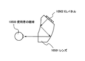
図32を参照する。図32には、実施例1および実施例3のゴーグル型表示装置に用いることが可能なレンズと表示装置であるELパネルが示されている。10501はレンズ、10502はELパネル、10503は使用者の眼球である。10502のELパネルに映し出された画像は10501のレンズを通って拡大され、10503の使用者の眼球内の網膜上に投影される。本実施例において、レンズの形状は実施例1および実施例3と異なり、使用者の見るレンズの表面が平面になっている。
【0168】
(実施例15)
【0169】
図33を参照する。図33には、実施例1および実施例3のゴーグル型表示装置に用いることが可能なレンズと表示装置であるELパネルが示されている。本実施例において、レンズの形状は実施例1、2または3と異なり、画像がレンズ内で移動する距離が長くなるように設計されている。10601はレンズ、10602はELパネル、10603は使用者の眼球である。10602のELパネルに映し出された画像は10601のレンズを通って拡大され、レンズ内で3回反射した後、10603の使用者の眼球内の網膜上に投影される。
【0170】
(実施例16)
【0171】
図34を参照する。図34には、実施例1および実施例3のゴーグル型表示装置に用いることが可能なレンズと表示装置であるELパネルが示されている。本実施例においては、レンズの形状が実施例1、2、3または4と異なる。10701はレンズ、10702はELパネル、10703は使用者の眼球である。10702のELパネルに映し出された画像は10701のレンズを通って拡大され、レンズ内で4回反射した後、10703の使用者の眼球内の網膜上に投影される。
【0172】
(実施例17)
【0173】
図35を参照する。図35には、実施例1および実施例3のゴーグル型表示装置に用いることが可能なレンズと表示装置であるELパネルが示されている。本実施例において、レンズの形状は実施例1、2、3、4または5と異なり、2つのレンズによって構成されている。10801aおよび10801bはレンズ、10802はELパネル、10803は使用者の眼球、10807はハーフミラーである。10802のELパネルに映し出された画像は10801bのレンズ、10807のハーフミラー、10801aのレンズを通ったのち拡大される。再び、10801aのレンズを通ったのち10807のハーフミラーで反射した後、10803の使用者の眼球内の網膜上に投影される。
【0174】
(実施例18)
【0175】
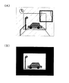
図36を参照する。図36には、本実施例のゴーグル型表示装置が示されている。本実施例においては、ゴーグル型表示装置に前方の光景を観察するための透明窓10904Rと10904Lが設けられており、実施例1と異なる。これにより、使用者は図37(A)のようにゴーグル型表示装置の前方の光景と、表示装置に表示された画像とを同時に見ることが可能である。スイッチ10905は、図37(A)のようなゴーグル型表示装置の前方の光景と、表示装置に表示された画像とが同時に見えるモードと、図37(B)のように表示装置に表示された画像のみが見えるモードとを切り替えるものである。
【0176】
図38は図36におけるDの部分を切断したときの断面図である。図38において、10901Raと10901Rbはレンズ、10902RはELパネル、10903Rは使用者の眼球である。前方の光景は10904Rの透明窓、10906Rのシャッター、10901Rbのレンズ、10907Rのハーフミラー、10901Raのレンズ、10910Rの観察用透明窓を通して観察することが出来る。10902RのELパネルに映し出された画像は10901Rbのレンズ、10907Rのハーフミラー、10901Raのレンズを通ったのち拡大される。再び、10901Raのレンズを通ったのち10907Rのハーフミラーで反射した後、10903Rの使用者の眼球内の網膜上に投影される。
【0177】
10905Rのフレア防止枠は、外光による有害光を装置内部へ入射させないように設置されており、装置本体10900と一体になっていても、別に構成されていてもかまわない。
【0178】
10906Rのシャッターは、スイッチ10905を使用することにより、10904Rの透明窓を通して見える前方の光景をさえぎったり透過させたりする働きがある。これは光をさえぎれるものでも、液晶のように光学異方性を有するものでもかまわない。
【0179】
本実施例で用いることが可能な光学素子は、本実施例で説明したものに限定しない。
【0180】
(実施例19)
本実施例では、本願発明に用いるEL(エレクトロルミネッセンス)パネルの作製例について説明する。
【0181】
図39(A)は本実施例で説明するELパネルの上面図である。図39(A)において、14010は基板、14011は画素部、14012はゲート側駆動回路、14013はソース側駆動回路であり、それぞれの駆動回路は配線14014〜14016を経てFPC14017に至り、外部機器へと接続される。
【0182】
このとき、少なくとも画素部、好ましくは駆動回路及び画素部を囲むようにしてカバー材16000、シーリング材(ハウジング材ともいう)17000、密封材(第2のシーリング材)17001が設けられている。
【0183】
また、図39(B)は図39(A)をC−C‘で切断した断面であり、基板14010、下地膜14021の上に駆動回路用TFT(但し、ここではnチャネル型TFTとpチャネル型TFTを組み合わせたCMOS回路)、14022及び画素部用TFT14023(但し、ここではEL素子への電流を制御するTFTだけ図示している。)が形成されている。これらのTFTは公知の構造(トップゲート構造またはボトムゲート構造)を用いれば良い。
【0184】
公知の作製方法を用いて駆動回路用TFT14022、画素部用TFT14023が完成したら、樹脂材料でなる層間絶縁膜(平坦化膜)14026の上に画素部用TFT14023のドレインと電気的に接続する透明導電膜でなる画素電極14027を形成する。透明導電膜としては、酸化インジウムと酸化スズとの化合物(ITOと呼ばれる)または酸化インジウムと酸化亜鉛との化合物を用いることができる。そして、画素電極14027を形成したら、絶縁膜14028を形成し、画素電極14027上に開口部を形成する。
【0185】
次に、EL層14029を形成する。EL層14029は公知のEL材料(正孔注入層、正孔輸送層、発光層、電子輸送層または電子注入層)を自由に組み合わせて積層構造または単層構造とすれば良い。どのような構造とするかは公知の技術を用いれば良い。また、EL材料には低分子系材料と高分子系(ポリマー系)材料がある。低分子系材料を用いる場合は蒸着法を用いるが、高分子系材料を用いる場合には、スピンコート法、印刷法またはインクジェット法等の簡易な方法を用いることが可能である。
【0186】
本実施例では、シャドーマスクを用いて蒸着法によりEL層を形成する。シャドーマスクを用いて画素毎に波長の異なる発光が可能な発光層(赤色発光層、緑色発光層及び青色発光層)を形成することで、カラー表示が可能となる。その他にも、色変換層(CCM)とカラーフィルターを組み合わせた方式、白色発光層とカラーフィルターを組み合わせた方式があるがいずれの方法を用いても良い。勿論、単色発光のEL表示装置とすることもできる。
【0187】
EL層14029を形成したら、その上に陰極14030を形成する。陰極14030とEL層14029の界面に存在する水分や酸素は極力排除しておくことが望ましい。従って、真空中でEL層14029と陰極14030を連続成膜するか、EL層14029を不活性雰囲気で形成し、大気解放しないで陰極14030を形成するといった工夫が必要である。本実施例ではマルチチャンバー方式(クラスターツール方式)の成膜装置を用いることで上述のような成膜を可能とする。
【0188】
なお、本実施例では陰極14030として、LiF(フッ化リチウム)膜とAl(アルミニウム)膜の積層構造を用いる。具体的にはEL層14029上に蒸着法で1nm厚のLiF(フッ化リチウム)膜を形成し、その上に300nm厚のアルミニウム膜を形成する。勿論、公知の陰極材料であるMgAg電極を用いても良い。そして陰極14030は14031で示される領域において配線14016に接続される。配線14016は陰極14030に所定の電圧を与えるための電源供給線であり、導電性ペースト材料14032を介してFPC14017に接続される。
【0189】
14031に示された領域において陰極14030と配線14016とを電気的に接続するために、層間絶縁膜14026及び絶縁膜14028にコンタクトホールを形成する必要がある。これらは層間絶縁膜14026のエッチング時(画素電極用コンタクトホールの形成時)や絶縁膜14028のエッチング時(EL層形成前の開口部の形成時)に形成しておけば良い。また、絶縁膜14028をエッチングする際に、層間絶縁膜14026まで一括でエッチングしても良い。この場合、層間絶縁膜14026と絶縁膜14028が同じ樹脂材料であれば、コンタクトホールの形状を良好なものとすることができる。
【0190】
このようにして形成されたEL素子の表面を覆って、パッシベーション膜16003、充填材16004、カバー材16000が形成される。
【0191】
さらに、EL素子部を囲むようにして、カバー材16000と基板14010の内側にシーリング材17000が設けられ、さらにシーリング材17000の外側には密封材(第2のシーリング材)17001が形成される。
【0192】
このとき、この充填材16004は、カバー材16000を接着するための接着剤としても機能する。充填材16004としては、PVC(ポリビニルクロライド)、エポキシ樹脂、シリコーン樹脂、PVB(ポリビニルブチラル)またはEVA(エチレンビニルアセテート)を用いることができる。この充填材16004の内部に乾燥剤を設けておくと、吸湿効果を保持できるので好ましい。
【0193】
また、充填材16004の中にスペーサーを含有させてもよい。このとき、スペーサーをBaOなどからなる粒状物質とし、スペーサー自体に吸湿性をもたせてもよい。
【0194】
スペーサーを設けた場合、パッシベーション膜16003はスペーサー圧を緩和することができる。また、パッシベーション膜とは別に、スペーサー圧を緩和する樹脂膜などを設けてもよい。
【0195】
また、カバー材16000としては、ガラス板、アルミニウム板、ステンレス板、FRP(Fiberglass−Reinforced Plastics)板、PVF(ポリビニルフルオライド)フィルム、マイラーフィルム、ポリエステルフィルムまたはアクリルフィルムを用いることができる。なお、充填材16004としてPVBやEVAを用いる場合、数十μmのアルミニウムホイルをPVFフィルムやマイラーフィルムで挟んだ構造のシートを用いることが好ましい。
【0196】
但し、EL素子からの発光方向(光の放射方向)によっては、カバー材16000が透光性を有する必要がある。
【0197】
また、配線14016はシーリング材17000および密封材17001と基板14010との隙間を通ってFPC14017に電気的に接続される。なお、ここでは配線14016について説明したが、他の配線14014、14015も同様にしてシーリング材17000および密封材17001の下を通ってFPC14017に電気的に接続される。
【0198】
なお本実施例では、充填材16004を設けてからカバー材16000を接着し、充填材16004の側面(露呈面)を覆うようにシーリング材17000を取り付けているが、カバー材16000及びシーリング材17000を取り付けてから、充填材16004を設けても良い。この場合、基板14010、カバー材16000及びシーリング材17000で形成されている空隙に通じる充填材の注入口を設ける。そして前記空隙を真空状態(10-2Torr以下)にし、充填材の入っている水槽に注入口を浸してから、空隙の外の気圧を空隙の中の気圧よりも高くして、充填材を空隙の中に充填する。
【0199】
(実施例20)
本実施例では、実施例9とは異なる形態のELパネルを作製した例について、図40(A)、40(B)を用いて説明する。図39(A)、39(B)と同じ番号のものは同じ部分を指しているので説明は省略する。
【0200】
図40(A)は本実施例のELパネルの上面図であり、図40(A)をC-C'で切断した断面図を図40(B)に示す。
【0201】
実施例9に従って、EL素子の表面を覆ってパッシベーション膜16003までを形成する。
【0202】
さらに、EL素子を覆うようにして充填材16004を設ける。この充填材16004は、カバー材16000を接着するための接着剤としても機能する。充填材16004としては、PVC(ポリビニルクロライド)、エポキシ樹脂、シリコーン樹脂、PVB(ポリビニルブチラル)またはEVA(エチレンビニルアセテート)を用いることができる。この充填材16004の内部に乾燥剤を設けておくと、吸湿効果を保持できるので好ましい。
【0203】
また、充填材16004の中にスペーサーを含有させてもよい。このとき、スペーサーをBaOなどからなる粒状物質とし、スペーサー自体に吸湿性をもたせてもよい。
【0204】
スペーサーを設けた場合、パッシベーション膜16003はスペーサー圧を緩和することができる。また、パッシベーション膜とは別に、スペーサー圧を緩和する樹脂膜などを設けてもよい。
【0205】
また、カバー材16000としては、ガラス板、アルミニウム板、ステンレス板、FRP(Fiberglass−Reinforced Plastics)板、PVF(ポリビニルフルオライド)フィルム、マイラーフィルム、ポリエステルフィルムまたはアクリルフィルムを用いることができる。なお、充填材16004としてPVBやEVAを用いる場合、数十μmのアルミニウムホイルをPVFフィルムやマイラーフィルムで挟んだ構造のシートを用いることが好ましい。
【0206】
但し、EL素子からの発光方向(光の放射方向)によっては、カバー材16000が透光性を有する必要がある。
【0207】
次に、充填材16004を用いてカバー材16000を接着した後、充填材16004の側面(露呈面)を覆うようにフレーム材16001を取り付ける。フレーム材16001はシーリング材(接着剤として機能する)16002によって接着される。このとき、シーリング材16002としては、光硬化性樹脂を用いるのが好ましいが、EL層の耐熱性が許せば熱硬化性樹脂を用いても良い。なお、シーリング材16002はできるだけ水分や酸素を透過しない材料であることが望ましい。また、シーリング材16002の内部に乾燥剤を添加してあっても良い。
【0208】
また、配線14016はシーリング材16002と基板14010との隙間を通ってFPC14017に電気的に接続される。なお、ここでは配線14016について説明したが、他の配線14014、14015も同様にしてシーリング材16002の下を通ってFPC14017に電気的に接続される。
【0209】
なお本実施例では、充填材16004を設けてからカバー材16000を接着し、充填材16004の側面(露呈面)を覆うようにフレーム材16001を取り付けているが、カバー材16000及びフレーム材16001を取り付けてから、充填材16004を設けても良い。この場合、基板14010、カバー材16000及びフレーム材16001で形成されている空隙に通じる充填材の注入口を設ける。そして前記空隙を真空状態(10-2Torr以下)にし、充填材の入っている水槽に注入口を浸してから、空隙の外の気圧を空隙の中の気圧よりも高くして、充填材を空隙の中に充填する。
【0210】
(実施例21)
ここでELパネルにおける画素部のさらに詳細な断面構造を図41に、上面構造を図42(A)に、回路図を図42(B)に示す。図41、図42(A)及び図42(B)では共通の符号を用いるので互いに参照すれば良い。
【0211】
図41において、基板13501上に設けられたスイッチング用TFT13502は公知の方法で形成されたnチャネル型TFTを用いる。本実施例ではダブルゲート構造としているが、構造及び作製プロセスに大きな違いはないので説明は省略する。但し、ダブルゲート構造とすることで実質的に二つのTFTが直列された構造となり、オフ電流値を低減することができるという利点がある。なお、本実施例ではダブルゲート構造としているが、シングルゲート構造でも構わないし、トリプルゲート構造やそれ以上のゲート本数を持つマルチゲート構造でも構わない。また、公知の方法で形成されたpチャネル型TFTを用いて形成しても構わない。
【0212】
また、電流制御用TFT13503は公知の方法で形成されたnチャネル型TFTを用いる。そして、スイッチング用TFT13502のドレイン配線35は配線36によって電流制御用TFTのゲート電極37に電気的に接続されている。また、38で示される配線は、スイッチング用TFT13502のゲート電極39a、39bを電気的に接続するゲート配線である。
【0213】
電流制御用TFT13503はEL素子を流れる電流量を制御するための素子であるため、多くの電流が流れ、熱による劣化やホットキャリアによる劣化の危険性が高い素子でもある。そのため、電流制御用TFT13503のドレイン側に、ゲート絶縁膜を介してゲート電極に重なるようにLDD領域を設ける構造は極めて有効である。
【0214】
また、本実施例では電流制御用TFT13503をシングルゲート構造で図示しているが、複数のTFTを直列につなげたマルチゲート構造としても良い。さらに、複数のTFTを並列につなげて実質的にチャネル形成領域を複数に分割し、熱の放射を高い効率で行えるようにした構造としても良い。このような構造は熱による劣化対策として有効である。
【0215】
また、図42(A)に示すように、電流制御用TFT13503のゲート電極37となる配線36は13504で示される領域で、電流制御用TFT13503のドレイン配線40と絶縁膜を介して重なる。このとき、13504で示される領域ではコンデンサが形成される。保持容量13503は、電源供給線13506と電気的に接続された半導体膜13520、ゲート絶縁膜と同一層の絶縁膜(図示せず)及び配線36との間で形成される。また、配線36、第1層間絶縁膜と同一の層(図示せず)及び電源供給線13506で形成される容量も保持容量として用いることが可能である。このコンデンサ13504は電流制御用TFT13503のゲート電極37にかかる電圧を保持するためのコンデンサとして機能する。なお、電流制御用TFTのドレインは電源供給線(電源線)13506に接続され、常に一定の電圧が加えられている。
【0216】
スイッチング用TFT13502及び電流制御用TFT13503の上には第1パッシベーション膜41が設けられ、その上に樹脂絶縁膜でなる平坦化膜42が形成される。平坦化膜42を用いてTFTによる段差を平坦化することは非常に重要である。後に形成されるEL層は非常に薄いため、段差が存在することによって発光不良を起こす場合がある。従って、EL層をできるだけ平坦面に形成しうるように画素電極を形成する前に平坦化しておくことが望ましい。
【0217】
また、43は反射性の高い導電膜でなる画素電極(EL素子の陰極)であり、電流制御用TFT13503のドレインに電気的に接続される。画素電極43としてはアルミニウム合金膜、銅合金膜または銀合金膜など低抵抗な導電膜またはそれらの積層膜を用いることが好ましい。勿論、他の導電膜との積層構造としても良い。
【0218】
また、絶縁膜(好ましくは樹脂)で形成されたバンク44a、44bにより形成された溝(画素に相当する)の中に発光層45が形成される。なお図42(A)では、保持容量13504の位置を明確にするために一部バンクを省略しており、バンク44a、44bしか図示していないが、電源供給線13506とソース配線34を一部覆うように電源供給線13506とソース配線34の間に設けられている。また、ここでは二画素しか図示していないが、R(赤)、G(緑)、B(青)の各色に対応した発光層を作り分けても良い。発光層とする有機EL材料としてはπ共役ポリマー系材料を用いる。代表的なポリマー系材料としては、ポリパラフェニレンビニレン(PPV)系、ポリビニルカルバゾール(PVK)系、ポリフルオレン系などが挙げられる。
【0219】
なお、PPV系有機EL材料としては様々な型のものがあるが、例えば「H. Shenk,H.Becker,O.Gelsen,E.Kluge,W.Kreuder,and H.Spreitzer,“Polymers for Light Emitting Diodes”,Euro Display,Proceedings,1999,p.33-37」や特開平10−92576号公報に記載されたような材料を用いれば良い。
【0220】
具体的な発光層としては、赤色に発光する発光層にはシアノポリフェニレンビニレン、緑色に発光する発光層にはポリフェニレンビニレン、青色に発光する発光層にはポリフェニレンビニレン若しくはポリアルキルフェニレンを用いれば良い。膜厚は30〜150nm(好ましくは40〜100nm)とすれば良い。
【0221】
但し、以上の例は発光層として用いることのできる有機EL材料の一例であって、これに限定する必要はまったくない。発光層、電荷輸送層または電荷注入層を自由に組み合わせてEL層(発光及びそのためのキャリアの移動を行わせるための層)を形成すれば良い。
【0222】
例えば、本実施例ではポリマー系材料を発光層として用いる例を示したが、低分子系有機EL材料を用いても良い。また、電荷輸送層や電荷注入層として炭化珪素等の無機材料を用いることも可能である。これらの有機EL材料や無機材料は公知の材料を用いることができる。
【0223】
本実施例では発光層45の上にPEDOT(ポリチオフェン)またはPAni(ポリアニリン)でなる正孔注入層46を設けた積層構造のEL層としている。そして、正孔注入層46の上には透明導電膜でなる陽極47が設けられる。本実施例の場合、発光層45で生成された光は上面側に向かって(TFTの上方に向かって)放射されるため、陽極は透光性でなければならない。透明導電膜としては酸化インジウムと酸化スズとの化合物や酸化インジウムと酸化亜鉛との化合物を用いることができるが、耐熱性の低い発光層や正孔注入層を形成した後で形成するため、可能な限り低温で成膜できるものが好ましい。
【0224】
陽極47まで形成された時点でEL素子13505が完成する。なお、ここでいうEL素子13505は、画素電極(陰極)43、発光層45、正孔注入層46及び陽極47で形成されたコンデンサを指す。図42(A)に示すように画素電極43は画素の面積にほぼ一致するため、画素全体がEL素子として機能する。従って、発光の利用効率が非常に高く、明るい画像表示が可能となる。
【0225】
ところで、本実施例では、陽極47の上にさらに第2パッシベーション膜48を設けている。第2パッシベーション膜48としては窒化珪素膜または窒化酸化珪素膜が好ましい。この目的は、外部とEL素子とを遮断することであり、有機EL材料の酸化による劣化を防ぐ意味と、有機EL材料からの脱ガスを抑える意味との両方を併せ持つ。これによりEL表示装置の信頼性が高められる。
【0226】
以上のように本願発明で使用するEL表示パネルは図41のような構造の画素からなる画素部を有し、オフ電流値の十分に低いスイッチング用TFTと、ホットキャリア注入に強い電流制御用TFTとを有する。従って、高い信頼性を有し、且つ、良好な画像表示が可能なEL表示パネルが得られる。
【0227】
〔実施例22〕
本実施例では、実施例21に示した画素部において、EL素子13505の構造を反転させた構造について説明する。説明には図43を用いる。なお、図41の構造と異なる点はEL素子の部分と電流制御用TFTだけであるので、その他の説明は省略することとする。
【0228】
図43において、電流制御用TFT13503は公知の方法で形成されたpチャネル型TFTを用いる。
【0229】
本実施例では、画素電極(陽極)50として透明導電膜を用いる。具体的には酸化インジウムと酸化亜鉛との化合物でなる導電膜を用いる。勿論、酸化インジウムと酸化スズとの化合物でなる導電膜を用いても良い。
【0230】
そして、絶縁膜でなるバンク51a、51bが形成された後、溶液塗布によりポリビニルカルバゾールでなる発光層52が形成される。その上にはカリウムアセチルアセトネート(acacKと表記される)でなる電子注入層53、アルミニウム合金でなる陰極54が形成される。この場合、陰極54がパッシベーション膜としても機能する。こうしてEL素子13701が形成される。
【0231】
本実施例の場合、発光層52で発生した光は、矢印で示されるようにTFTが形成された基板の方に向かって放射される。
【0232】
〔実施例23〕
本実施例では、図42(B)に示した回路図とは異なる構造の画素とした場合の例について図44(A)〜(C)に示す。なお、本実施例において、13801はスイッチング用TFT13802のソース配線、13803はスイッチング用TFT13802のゲート配線、13804は電流制御用TFT、13805はコンデンサ、13806、13808は電源供給線、13807はEL素子とする。
【0233】
図44(A)は、二つの画素間で電源供給線13806を共通とした場合の例である。即ち、二つの画素が電源供給線13806を中心に線対称となるように形成されている点に特徴がある。この場合、電源供給線の本数を減らすことができるため、画素部をさらに高精細化することができる。
【0234】
また、図44(B)は、電源供給線13808をゲート配線13803と平行に設けた場合の例である。なお、図44(B)では電源供給線13808とゲート配線13803とが重ならないように設けた構造となっているが、両者が異なる層に形成される配線であれば、絶縁膜を介して重なるように設けることもできる。この場合、電源供給線13808とゲート配線13803とで専有面積を共有させることができるため、画素部をさらに高精細化することができる。
【0235】
また、図44(C)は、図44(B)の構造と同様に電源供給線13808をゲート配線13803と平行に設け、さらに、二つの画素を電源供給線13808を中心に線対称となるように形成する点に特徴がある。また、電源供給線13808をゲート配線13803のいずれか一方と重なるように設けることも有効である。この場合、電源供給線の本数を減らすことができるため、画素部をさらに高精細化することができる。
【0236】
(実施例24)
実施例21に示した図42(A)、42(B)では電流制御用TFT13503のゲートにかかる電圧を保持するためにコンデンサ13504を設ける構造としているが、コンデンサ13504を省略することも可能である。実施例10の場合、電流制御用TFT13503として公知の方法で形成されたnチャネル型TFTを用いているため、ゲート絶縁膜を介してゲート電極に重なるように設けられたLDD領域を有している。この重なり合った領域には一般的にゲート容量と呼ばれる寄生容量が形成されるが、本実施例ではこの寄生容量をコンデンサ13504の代わりとして積極的に用いる点に特徴がある。
【0237】
この寄生容量のキャパシタンスは、上記ゲート電極とLDD領域とが重なり合った面積によって変化するため、その重なり合った領域に含まれるLDD領域の長さによって決まる。
【0238】
また、実施例23に示した図44(A),(B),(C)の構造においても同様に、コンデンサ13805を省略することは可能である。
【0239】
【発明の効果】
【0240】
本発明のゴーグル型表示装置によると、レンズ等の光学素子と液晶パネルが一体となっているので、従来問題となっていた、液晶パネルとレンズとの「ずれ」による表示品質の劣化を防ぐことができる。
【図面の簡単な説明】
【図1】 本発明のゴーグル型表示装置の光学素子、表示素子等の構成を示した図である。
【図2】 本発明のゴーグル型表示装置の実施例の概略構成図である。
【図3】 本発明のゴーグル型表示装置の実施例の断面図である。
【図4】 本発明のゴーグル型表示装置の実施例の液晶パネルの概略ブロック図である。
【図5】 本発明のゴーグル型表示装置の実施例の液晶パネルの概略ブロック図である。
【図6】 本発明のゴーグル型表示装置の実施例の液晶パネルの回路図である。
【図7】 本発明のゴーグル型表示装置の実施例のD/A変換回路の回路図である。
【図8】 本発明のゴーグル型表示装置の実施例の概略構成図である。
【図9】 本発明のゴーグル型表示装置の実施例の概略構成図である。
【図10】 本発明のゴーグル型表示装置の実施例の概略構成図である。
【図11】 本発明のゴーグル型表示装置の実施例の概略構成図である。
【図12】 本発明のゴーグル型表示装置の実施例の概略構成図である。
【図13】 本発明のゴーグル型表示装置の実施例の概略構成図である。
【図14】 本発明のゴーグル型表示装置の実施例の概略構成図である。
【図15】 本発明のゴーグル型表示装置の実施例の概略構成図である。
【図16】 本発明のゴーグル型表示装置の実施例の概略構成図である。
【図17】 本発明のゴーグル型表示装置の実施例の概略構成図である。
【図18】 本発明のゴーグル型表示装置の実施例の概略構成図である。
【図19】 本発明のゴーグル型表示装置の実施例の概略構成図である。
【図20】 本発明のゴーグル型表示装置の実施例の概略構成図である。
【図21】 本発明のゴーグル型表示装置の実施例の概略構成図である。
【図22】 本発明のゴーグル型表示装置に用いられる液晶パネルの作製工程例である。
【図23】 本発明のゴーグル型表示装置に用いられる液晶パネルの作製工程例である。
【図24】 本発明のゴーグル型表示装置に用いられる液晶パネルの作製工程例である。
【図25】 本発明のゴーグル型表示装置に用いられる液晶パネルの作製工程例である。
【図26】 本発明のゴーグル型表示装置に用いられる液晶パネルの作製工程例である。
【図27】 無しきい値反強誘電性混合液晶のV字型の電気光学特性を示すグラフである。
【図28】 本発明のゴーグル型表示装置の光学素子とELパネルなどの構成を示した図である。
【図29】 実施例11の両眼用ゴーグル型表示装置の概略図である。
【図30】 実施例12の両眼用ゴーグル型表示装置の断面図である。
【図31】 実施例13の片目用ゴーグル型表示装置の概略図である。
【図32】 実施例14の光学素子とELパネルなどの構成を示した図である。
【図33】 実施例15の光学素子とELパネルなどの構成を示した図である。
【図34】 実施例16の光学素子とELパネルなどの構成を示した図である。
【図35】 実施例17の光学素子とELパネルなどの構成を示した図である。
【図36】 実施例18の両眼用ゴーグル型表示装置の断面図である。
【図37】 実施例18の眼球の網膜上に投影される像である。
【図38】 実施例18の両眼用ゴーグル型表示装置の断面図である。
【図39】 実施例19で用いるELパネルの上面図および断面図である。
【図40】 実施例20で用いるELパネルの上面図および断面図である。
【図41】 実施例21で用いるELパネルの画素部の断面図である。
【図42】 実施例21で用いるELパネルの上面構造図および回路図である。
【図43】 実施例22で用いるELパネルの画素部の断面図である。
【図44】 実施例23で用いるELパネルの回路図である。
【図45】 液晶パネルを用いた場合の光学素子と表示装置の構成である。
【符号の説明】
101 レンズ
102 液晶パネル
103 バックライト
104 使用者の眼球[0001]
BACKGROUND OF THE INVENTION
[0002]
The invention disclosed in this specification relates to a goggle type display device. In this specification, the goggle type display device is referred to as a head mounted display (HMD).
[0003]
[Prior art]
[0004]
In recent years, goggle type display devices that users wear on their heads have become widespread. This goggle type display device is also called HMD (Head Mounted Display), a lens for enlarging an image to form a virtual image thereof, and a display device such as a liquid crystal panel installed closer to the focal length of the lens have. The user can view the enlarged image by observing the display on the liquid crystal panel through the lens. Therefore, it is possible to appreciate the display on the large screen while being small.
[0005]
Refer to FIG. The image displayed on the liquid crystal panel 11802 passes through the lens 11801 and is projected onto the retina in the eyeball of the user 11803. At this time, it is necessary to use 11805A and 11805B polarizing plates on the 11802 liquid crystal panel and to use the 11804 backlight that uniformly shines in the plane as a light source.
[0006]
The goggle type display device that can be used while moving can be seen from the gap between the display and the face for safety.
[0007]
[Problems to be solved by the invention]
[0008]
Since the goggle type display device is used by being worn on the head as described above, the goggle type display device is required to have a higher impact resistance of the main body than the stationary display device. In addition, the goggle type display device always moves during use, and the internal optical system is likely to cause a “displacement” as compared with the stationary type display device.
[0009]
Since the goggle type display device observes the display of the liquid crystal panel through the lens, there has been a problem that “displacement” between the liquid crystal panel and the lens directly leads to deterioration of display quality.
[0010]
The goggle type display device is required to be reduced in size and weight because the user wears it on the head. In addition, since it is carried and used, further reduction in power consumption is required.
[0011]
Accordingly, the present invention has been made in view of the above problems, and an object thereof is to provide a goggle type display device that solves the above problems.
[0012]
[Means for Solving the Problems]
[0013]
The present invention adopts the following means in order to solve the above-described problems. Please refer to FIG. FIG. 1 shows a lens which is an optical element used in the goggle type display device of the present invention, a liquid crystal panel and a backlight which are image display components. According to the present invention, the liquid crystal panel is fixed to the lens, and the relative position between the liquid crystal panel and the lens does not shift.
[0014]
In FIG. 1, 101 is a lens, 102 is a liquid crystal panel, 103 is a backlight, and 104 is a user's eyeball. The lens 101 has a groove in which the liquid crystal panel is fixed in advance, and the liquid crystal panel 102 is incorporated in the groove.
[0015]
Note that the backlight 103 may be fixed to a liquid crystal panel or a lens.
[0016]
As described above, according to the present invention, the relative position between the liquid crystal panel for displaying an image and the optical element (lens) for enlarging the image and projecting it on the user's eyeball does not change with time. Therefore, the relative position between the liquid crystal panel and the lens is maintenance-free.
[0017]
The present invention adopts the following means in order to solve the above-described problems. The goggle type display device of the present invention includes an audio reproduction device, a self-luminous EL panel as a display device, and an optical element composed of a prism, a lens, a mirror and the like for enlarging a displayed image and guiding it to the eyes And a driving device for controlling the sound reproducing device and the display device. The EL panel is also called an organic EL display (OELD) or an organic light emitting diode (OLED). By using a self-luminous EL panel, unlike a liquid crystal panel, a high-luminance image can be provided to a user without using a backlight. Further, since no backlight is used, power consumption can be reduced.
[0018]
In addition, when using a liquid crystal panel, a fixture for fixing the relative positions of the optical element, the liquid crystal panel, and the backlight so that they do not shift is necessary. When using an EL panel, the optical element and the EL panel are only fixed so that they do not deviate from each other. Therefore, the deviation is less likely to occur, and the weight of the backlight can be reduced compared to using a liquid crystal panel. Can be reduced in weight.
[0019]
Further, unlike the liquid crystal panel, the EL panel does not require the use of a polarizing plate, so that the luminance is not lowered by using the polarizing plate.
[0020]
Note that the audio reproduction device may not be provided.
[0021]
According to the present invention,
A display device;
An optical element;
A goggle type display device comprising:
The goggle type display device is provided in which the display device and the optical element are integrated.
[0022]
According to the present invention,
A display device;
A lens for enlarging an image displayed by the display device;
A goggle type display device comprising:
The goggle type display device is provided in which the display device and the lens are integrated.
[0023]
According to the present invention,
A display device;
A lens for enlarging an image displayed by the display device;
A goggle type display device comprising:
A goggle type display device is provided, wherein the display device is incorporated in a part of the lens.
[0024]
According to the present invention,
A display device;
An optical element;
A goggle type display device comprising:
The goggle type display device is provided in which the display device and the optical element are integrally formed.
[0025]
According to the present invention,
A display device;
A lens for enlarging an image displayed by the display device;
A goggle type display device comprising:
The goggle type display device is provided in which the display device and the lens are integrally formed.
[0026]
According to the present invention,
The goggle type display device according to any one of
[0027]
According to the present invention,
8. The display device according to
[0028]
According to the present invention,
The liquid crystal panel according to claim 8, wherein the liquid crystal material is an antiferroelectric mixed liquid crystal having a V-shaped electro-optical characteristic.
[0029]
According to the present invention,
The diagonal size of the pixel portion of the liquid crystal panel is 2 inches or less, the channel width of the pixel TFT of the liquid crystal panel is 0.2 μm to 2 μm, and the active layer thickness of the pixel TFT is 10 nm to 50 nm. A liquid crystal panel according to any one of claims 7 to 9 is provided.
[0030]
In the above configuration,
It is provided that the channel width of the pixel TFT is 0.2 μm or more and 1.3 μm or less.
[0031]
According to the present invention,
A display device for inputting a video signal and displaying the video;
An optical element;
A goggle type display device comprising:
There is provided a goggle type display device characterized in that the display device comprises an EL element.
[0032]
According to the present invention,
A display device for inputting a video signal and displaying the video;
A lens for enlarging an image displayed by the display device;
A goggle type display device comprising:
There is provided a goggle type display device characterized in that the display device comprises an EL element.
[0033]
According to the present invention,
Two sets of display devices for inputting video signals and displaying video;
Two sets of optical elements;
A binocular goggle type display device comprising:
There is provided a goggle type display device characterized in that the display device comprises an EL element.
[0034]
According to the present invention,
Two sets of display devices for inputting video signals and displaying video;
Two sets of lenses for enlarging the image displayed by the display device;
A binocular goggle type display device comprising:
There is provided a goggle type display device characterized in that the display device comprises an EL element.
[0035]
According to the present invention,
A set of display devices for inputting video signals and displaying video;
A set of optical elements;
A one-eye goggle type display device comprising:
There is provided a goggle type display device characterized in that the display device comprises an EL element.
[0036]
According to the present invention,
A set of display devices for inputting video signals and displaying video;
A set of lenses for enlarging an image displayed by the display device;
A one-eye goggle type display device comprising:
There is provided a goggle type display device characterized in that the display device comprises an EL element.
[0037]
According to the present invention,
Two sets of display devices for inputting video signals and displaying video;
Magnifying the video displayed by the display device,
And two sets of lenses that transmit the front scene,
A binocular goggle type display device comprising:
There is provided a goggle type display device characterized in that the display device comprises an EL element.
[0038]
DETAILED DESCRIPTION OF THE INVENTION
[0039]
Hereinafter, the goggle type display device of the present invention will be described in detail with reference to examples. The goggle type display device of the present invention is not limited to the following examples.
[0040]
Example 1
[0041]
Please refer to FIG. FIG. 2 shows a schematic configuration diagram of the goggle type display device of this embodiment.
[0042]
FIG. 3 is a cross-sectional view of the part A in FIG. 2 of the goggle type display device of this embodiment. As shown in FIGS. 2 and 3, in this embodiment, a
[0043]
The
[0044]
Here, an outline of the
[0045]
[0046]
Reference is now made to FIG. FIG. 5 is a schematic configuration diagram showing the source driver of the liquid crystal panel of this embodiment in particular detail. 202R-1-1 is a source driver. 202R-1-2 is a gate driver.
[0047]
The
[0048]
202R-1-2 is a gate driver, and includes a shift register circuit, a buffer circuit, a level shifter circuit, and the like (all not shown).
[0049]
The
[0050]
Here, the operation and signal flow of the active matrix type liquid crystal panel of this embodiment will be described.
[0051]
First, the operation of the source driver will be described. A clock signal (CK) and a start pulse (SP) are input to the shift register circuit 501. The shift register circuit 501 sequentially generates timing signals based on the clock signal (CK) and the start pulse (SP), and sequentially supplies the timing signals to subsequent circuits through a buffer circuit or the like (not shown).
[0052]
A timing signal from the shift register circuit 501 is buffered by a buffer circuit or the like. Since many circuits or elements are connected to the source signal line to which the timing signal is supplied, the load capacitance (parasitic capacitance) is large. This buffer circuit is provided in order to prevent “dullness” of the rise of the timing signal caused by the large load capacity.
[0053]
The timing signal buffered by the buffer circuit is supplied to the latch circuit 1 (502). The latch circuit 1 (502) has 960 stages of latch circuits for processing 8-bit digital video data. When the timing signal is input, the latch circuit 1 (502) sequentially captures and holds 8-bit digital video data supplied from the digital video
[0054]
The time until the writing of digital video data to all the latch circuits in all stages of the latch circuit 1 (502) is called a line period. That is, from the time when writing of digital video data to the latch circuit of the leftmost stage in the latch circuit 1 (502) is started, the time of writing of digital video data to the latch circuit of the rightmost stage is completed. The time interval until is the line period. Actually, a period obtained by adding a horizontal blanking period to the line period may be called a line period.
[0055]
After the end of one line period, a latch signal (Latch Signal) is supplied to the latch circuit 2 (503) in accordance with the operation timing of the shift register circuit 501. At this moment, the digital video data written and held in the latch circuit 1 (502) is sent all at once to the latch circuit 2 (503), and is written and held in the latch circuits of all stages of the latch circuit 2 (503). Is done.
[0056]
The digital video data supplied from the digital video data dividing circuit is written again to the latch circuit 1 (502) which has finished sending the digital video data to the latch circuit 2 (503) based on the timing signal from the shift register circuit 501. Are performed sequentially.
[0057]
During the second line period, the digital video data written and held in the latch circuit 2 (503) is sequentially selected by the selector circuit 1 (504) and supplied to the D / A conversion circuit 505. Is done. In this embodiment, in the selector circuit 1 (504), one selector circuit corresponds to four source signal lines.
[0058]
As the selector circuit, the one described in Japanese Patent Application No. 9-286098, which is a patent application by the present applicant, can be used.
[0059]
The 8-bit digital video data from the latch circuit 2 (503) selected by the selector circuit 504 is supplied to the D / A conversion circuit 505. Here, the D / A conversion circuit used in this embodiment will be described with reference to FIG.
[0060]
FIG. 7 shows a circuit diagram of the D / A conversion circuit of this embodiment. Note that the D / A conversion circuit of this embodiment includes a level shifter circuit (LS) 505-2, but the level shifter circuit may be omitted and designed. In the level shifter circuit, when the signal Lo is input to the input IN and the signal Hi is input to the input INb, the high potential power supply VddHI is output from the output OUT and the low potential power supply Vss is output from the output OUTb. ing. Further, when the signal Hi is input to the input IN and the signal Lo is input to the input INb, the high potential power supply Vss is output from the output OUT, and the low potential power supply VddHI is output from the output OUTb.
[0061]
In the D / A conversion circuit of this embodiment, inverted data of digital video data A0 to A7 (herein referred to as inverted A0 to inverted A7) is input to one input of the NOR circuit (505-1). It has become. The reset pulse A (ResA) is input to the other input of the NOR circuit (505-1). The reset pulse A is input during the reset period TR of the D / A conversion circuit. In this embodiment, the digital video data (inverted A0 to A7) is input to the NOR circuit (505-1) even during the reset period TR. However, while the reset pulse ResA is input to the NOR circuit, NOR is performed. Digital video data is not output from the circuit.
[0062]
Note that the NOR circuit may be omitted, and digital video data (inverted A0 to A7) may be input after the reset period TR ends.
[0063]
After the reset period TR ends, the data writing period TE starts, and the 8-bit digital video data is raised in voltage by the level shifter circuit and input to the switch circuits SW0 to SW7.
[0064]
Each of the switch circuits SW0 to SW7 is composed of two analog switches ASW1 and ASW2. One end of ASW1 is connected to DC_VIDEO_L, and the other end is connected to one end of ASW2 and connected to a capacitor. One end of each ASW2 is connected to DC_VIDEO_H, and the other end is connected to one end of ASW2 and connected to a capacitor (1pF, 2pF, 4pF, 8pF, 1pF, 2pF, 4pF, 8pF). One end of each capacitor is connected to two analog switches, and the other end is connected to a reset switch 2 (Res2). One end of the reset switch 1 (Res1) is connected to DC_VIDEO_M, and the other end is connected to one end of a capacitor corresponding to the upper bit. A reset pulse (ResB) and an inverted reset pulse (inverted ResB) are input to the reset switches Res1 and Res2.
[0065]
Further, a capacitor (1 pF) is provided at a connection point between the circuit corresponding to the upper bit and the circuit corresponding to the lower bit. In the present embodiment, all the above-mentioned capacities are not limited to those values.
[0066]
The D / A conversion circuit 505 converts 8-bit digital video data into an image signal (gradation voltage), and sequentially supplies it to the source signal line selected by the selector circuit 2 (506).
[0067]
The image signal supplied to the source signal line is supplied to the source region of the pixel TFT of the pixel portion connected to the source signal line.
[0068]
In the
[0069]
In this manner, the corresponding pixel TFT is switched by the scanning signal from the gate driver, the image signal (gradation voltage) from the source driver is supplied to the pixel TFT, and the liquid crystal molecules are driven.
[0070]
[0071]
Here, the circuit configuration of the
[0072]
In this embodiment, the
[0073]
The liquid crystal panel of this embodiment performs so-called line-sequential driving that simultaneously drives pixels for one line (for example, P1,1, P1,2,..., And P1,1919). In other words, the image signal is simultaneously written in all the pixels for one line.
[0074]
(Example 2)
[0075]
Please refer to FIG. FIG. 8 shows a lens used in the goggle type display device of this embodiment, a liquid crystal panel and a backlight as image display components. In this embodiment, the shape of the lens is different from that of the first embodiment. According to this embodiment, the liquid crystal panel is fixed to the lens, and the relative position between the liquid crystal panel and the lens does not shift.
[0076]
In FIG. 8, 801 is a lens, 802 is a liquid crystal panel, 803 is a backlight, and 804 is a user's eyeball. The lens 801 has a groove in which the liquid crystal panel is fixed in advance, and the liquid crystal panel 802 is incorporated in the groove.
[0077]
Note that the backlight 803 may be fixed to a liquid crystal panel or a lens.
[0078]
FIG. 9 shows a cross-sectional view of the goggle type display device of this embodiment. In this embodiment, a liquid crystal panel 802R is incorporated in the groove of the lens 801R. Although not shown in FIG. 9, the liquid crystal panel 802R may be provided with a pair of polarizing plates or a single polarizing plate. Note that the liquid crystal panel 802R and the polarizing plate may be collectively referred to as a liquid crystal panel.
[0079]
(Example 3)
[0080]
Please refer to FIG. FIG. 10 shows a lens used in the goggle type display device of this embodiment, a liquid crystal panel and a backlight as image display components. In this embodiment, the shape of the lens is different from that in the first or second embodiment. According to this embodiment, the liquid crystal panel is fixed to the lens, and the relative position between the liquid crystal panel and the lens does not shift.
[0081]
In FIG. 10, 1001 is a lens, 1002 is a liquid crystal panel, 1003 is a backlight, and 1004 is a user's eyeball. The lens 1001 has a groove in which the liquid crystal panel is fixed in advance, and the liquid crystal panel 1002 is incorporated in the groove.
[0082]
Note that the backlight 1003 may be fixed to a liquid crystal panel or a lens.
[0083]
FIG. 11 shows a cross-sectional view of the goggle type display device of this embodiment. In this embodiment, a liquid crystal panel 1002R is incorporated in the groove of the lens 1001R. Although not shown in FIG. 11, the liquid crystal panel 1002R may be provided with a pair or one polarizing plate. Note that the liquid crystal panel 1002R and the polarizing plate may be collectively referred to as a liquid crystal panel.
[0084]
Example 4
[0085]
Please refer to FIG. FIG. 12 shows a lens used in the goggle type display device of the present embodiment, a liquid crystal panel as an image display component, and a backlight. In this embodiment, the shape of the lens is different from that of
[0086]
In FIG. 12, reference numeral 1201 denotes a lens, 1202 denotes a liquid crystal panel, 1203 denotes a backlight, and 1204 denotes a user's eyeball. The lens 1201 has a groove in which the liquid crystal panel is fixed in advance, and the liquid crystal panel 1202 is incorporated in the groove.
[0087]
Note that the backlight 1203 may be fixed to a liquid crystal panel or a lens.
[0088]
FIG. 13 is a cross-sectional view of the goggle type display device of this embodiment. In this embodiment, a liquid crystal panel 1202R is incorporated in the groove of the lens 1201R. Although not shown in FIG. 12, the liquid crystal panel 1202R may be provided with a pair or one polarizing plate.
[0089]
(Example 5)
[0090]
Refer to FIG. FIG. 14 shows a lens used in the goggle type display device of this embodiment, a liquid crystal panel and a backlight as image display components. In this embodiment, the shape of the lens is different from that of the first, second, third or fourth embodiment. According to this embodiment, the liquid crystal panel is fixed to the lens, and the relative position between the liquid crystal panel and the lens does not shift.
[0091]
In FIG. 14, reference numeral 1401 denotes a lens, 1402 denotes a liquid crystal panel, 1403 denotes a backlight, and 1404 denotes a user's eyeball. The lens 1401 has a groove in which the liquid crystal panel is fixed in advance, and the liquid crystal panel 1402 is incorporated in the groove.
[0092]
Note that the backlight 1403 may be fixed to a liquid crystal panel or a lens.
[0093]
FIG. 15 shows a sectional view of the goggle type display device of this embodiment. In this embodiment, a liquid crystal panel 1402R is incorporated in the groove of the lens 1401R. Although not shown in FIG. 15, the liquid crystal panel 1402R may be provided with a pair or one polarizing plate.
[0094]
(Example 6)
[0095]
Refer to FIG. FIG. 16 shows a schematic configuration diagram of the goggle type display device of the present embodiment.
[0096]
FIG. 17 shows a cross-sectional view of a portion B in FIG. 16 of the goggle type display device of this embodiment. As shown in FIG. 17, in this embodiment, the groove of the lens 2001R and the liquid crystal panel 2002R are integrally formed. FIG. 17 shows an enlarged view of the boundary between the groove of the lens 2001R and the liquid crystal panel 2002R. That is, a part of the lens 2001R functions as a counter substrate of the liquid crystal panel 2002R.
[0097]
2001R-1 is a counter electrode and 2001R-2 is an alignment film, both of which are formed on the lens 2001R side. 2002R-1 is a liquid crystal, 2002R-2 is a substrate, and 2002R-4 is a pixel TFT formed on the substrate. 2002R-3 is an alignment film formed on the substrate. In this embodiment, no polarizing plate is provided on the counter substrate side. A pair or one polarizing plate may be provided depending on the liquid crystal to be used.
[0098]
(Example 7)
[0099]
Please refer to FIG. FIG. 18 shows a schematic configuration diagram of the goggle type display device of the present embodiment.
[0100]
FIG. 19 shows a schematic block diagram of the
[0101]
Signal source coils 3100-1 and 3100-2 transmit signals supplied by the signal source as electromagnetic waves.
[0102]
Note that the rectifier circuit, the signal generation circuit, and the signal control circuit may be formed using an IC chip and fixed to a liquid crystal panel, a lens, or the like.
[0103]
(Example 8)
[0104]
FIG. 20 shows a lens 3101, a liquid crystal panel 3102, a backlight 3103,
[0105]
In this embodiment, the
[0106]
Note that the backlight 3103 may be fixed to a liquid crystal panel or a lens.
[0107]
Refer to FIG. FIG. 21 shows an example in which masks 3204 and 3205 are arranged at positions different from the above example in the goggle type display device of this embodiment.
[0108]
Example 9
[0109]
Here, a method for manufacturing a pixel TFT in the pixel portion and a driver circuit (a source driver, a gate driver, a D / A conversion circuit, or the like) provided on the periphery of the pixel portion on the same substrate will be described in detail according to the steps. In order to simplify the description, the control circuit is illustrated with a CMOS circuit, which is a basic circuit such as a shift register circuit, a buffer circuit, and a D / A conversion circuit, and an n-channel TFT.
[0110]
In FIG. 22A, a low alkali glass substrate or a quartz substrate can be used as the
[0111]
Next, a
[0112]
Then, a
[0113]
Then, the
[0114]
Then, a resist
[0115]
In order to form the LDD region of the n-channel TFT of the driver circuit, an impurity element imparting n-type conductivity is selectively added to the island-shaped
[0116]
Next, the
[0117]
Then, the
[0118]
Next, a first conductive layer is formed to form a gate electrode. The first conductive layer may be formed as a single layer, but may have a laminated structure such as two layers or three layers as necessary. In this example, a conductive layer (A) 6021 made of a conductive nitride metal film and a conductive layer (B) 6022 made of a metal film were laminated. The conductive layer (B) 6022 is an element selected from tantalum (Ta), titanium (Ti), molybdenum (Mo), and tungsten (W), an alloy containing the element as a main component, or an alloy film in which the elements are combined. (Typically, a Mo—W alloy film or a Mo—Ta alloy film). The conductive layer (A) 6021 is a tantalum nitride (TaN), tungsten nitride (WN), titanium nitride (TiN) film, or nitride. It is made of molybdenum (MoN). Alternatively, tungsten silicide, titanium silicide, or molybdenum silicide may be applied to the conductive layer (A) 6021 as an alternative material. In the conductive layer (B), the concentration of impurities contained in the conductive layer (B) should be reduced in order to reduce the resistance. In particular, the oxygen concentration should be 30 ppm or less. For example, tungsten (W) was able to realize a specific resistance value of 20 μΩcm or less by setting the oxygen concentration to 30 ppm or less.
[0119]
The conductive layer (A) 6021 may be 10 to 50 nm (preferably 20 to 30 nm), and the conductive layer (B) 6022 may be 200 to 400 nm (preferably 250 to 350 nm). In this embodiment, a 30 nm thick tantalum nitride film is used for the conductive layer (A) 6021 and a 350 nm Ta film is used for the conductive layer (B) 6022, both of which are formed by sputtering. In film formation by this sputtering method, if an appropriate amount of Xe or Kr is added to the sputtering gas Ar, the internal stress of the film to be formed can be relaxed and the film can be prevented from peeling. Although not shown, it is effective to form a silicon film doped with phosphorus (P) with a thickness of about 2 to 20 nm under the conductive layer (A) 6021. This improves adhesion and prevents oxidation of the conductive film formed thereon, and at the same time, an alkali metal element contained in a trace amount in the conductive layer (A) or the conductive layer (B) diffuses into the
[0120]
Next, resist
[0121]
Next, in order to form a source region and a drain region of the p-channel TFT of the driver circuit, a step of adding an impurity element imparting p-type is performed. Here, impurity regions are formed in a self-aligning manner using the
[0122]
Next, in the n-channel TFT, an impurity region functioning as a source region or a drain region was formed. Resist
[0123]
The
[0124]
Then, an impurity adding step for imparting n-type for forming the LDD region of the n-channel TFT of the pixel matrix circuit was performed. Here, an impurity element imparting n-type in a self-aligning manner is added by an ion doping method using the
[0125]
Thereafter, a heat treatment process is performed to activate the impurity element imparting n-type or p-type added at each concentration. This step can be performed by a furnace annealing method, a laser annealing method, or a rapid thermal annealing method (RTA method). Here, the activation process was performed by furnace annealing. The heat treatment is performed at 400 to 800 ° C., typically 500 to 600 ° C. in a nitrogen atmosphere having an oxygen concentration of 1 ppm or less, preferably 0.1 ppm or less. In this embodiment, heat treatment is performed at 550 ° C. for 4 hours. went. Further, in the case where a
[0126]
In this heat treatment, the conductive layers (C) 6028c to 6032c are formed to have a thickness of 5 to 80 nm from the surface of the metal films 6028b to 6032b forming the
[0127]
In the case where the island-shaped semiconductor layer was formed from an amorphous silicon film by a crystallization method using a catalytic element, a trace amount of the catalytic element remained in the island-shaped semiconductor layer. Of course, it is possible to complete the TFT even in such a state, but it is more preferable to remove at least the remaining catalyst element from the channel formation region. As one of means for removing the catalyst element, there is a means for utilizing the gettering action by phosphorus (P). The concentration of phosphorus (P) required for gettering is the impurity region (n) formed in FIG. + The catalytic element could be gettered from the channel formation regions of the n-channel TFT and the p-channel TFT by the heat treatment in the activation process performed here. (Fig. 24 (D))
[0128]
After the activation and hydrogenation steps are completed, a second conductive film is formed as a gate wiring. This second conductive film includes a conductive layer (D) mainly composed of aluminum (Al) or copper (Cu), which is a low resistance material, and titanium (Ti), tantalum (Ta), tungsten (W), molybdenum. It is good to form with the conductive layer (E) which consists of (Mo). In this embodiment, an aluminum (Al) film containing 0.1 to 2% by weight of titanium (Ti) is formed as the conductive layer (D) 6045, and a titanium (Ti) film is formed as the conductive layer (E) 6046. The conductive layer (D) 6045 may be 100 to 400 nm (preferably 250 to 350 nm), and the conductive layer (E) 6046 may be 50 to 200 (preferably 100 to 150 nm). (Fig. 25 (A))
[0129]
Then, in order to form a gate wiring connected to the gate electrode, the conductive layer (E) 6046 and the conductive layer (D) 6045 were etched to form
[0130]
The first
[0131]
Next, a silicon nitride film, a silicon oxide film, or a silicon nitride oxide film is formed as the
[0132]
Thereafter, a second
[0133]
In this way, a substrate having the TFT of the driving circuit and the pixel TFT of the pixel portion on the same substrate was completed. A p-channel TFT 6101, a first n-channel TFT 6102, and a second n-channel TFT 6103 are formed in the driver circuit, and a
[0134]
The p-channel TFT 6101 of the driver circuit includes a
[0135]
As described above, in this embodiment, it is possible to optimize the structure of the TFT constituting each circuit according to the specifications required by the pixel TFT and the drive circuit, and to improve the operation performance and reliability of the semiconductor device. Can do. Furthermore, the LDD region, the source region, and the drain region can be easily activated by forming the gate electrode from a heat-resistant conductive material, and the wiring resistance can be sufficiently reduced by forming the gate electrode from a low-resistance material. Therefore, the present invention can also be applied to a display device having a diagonal screen size of the pixel portion of 4 inch class or more.
[0136]
Further, the diagonal size of the pixel portion is 2 inches or less, the channel width of the pixel TFT is 0.2 μm to 2 μm (preferably 0.2 μm to 1.3 μm), and the activity of the pixel TFT The layer thickness may be 10 nm to 50 nm.
[0137]
(Example 10)
[0138]
In addition to the TN liquid crystal, various liquid crystals can be used for the liquid crystal panel manufactured according to the above embodiment. For example, 1998, SID, "Characteristics and Driving Scheme of Polymer-Stabilized Monostable FLCD Exhibiting Fast Response Time and High Contrast Ratio with Gray-Scale Capability" by H. Furue et al., 1997, SID DIGEST, 841, "A Full -Color Thresholdless Antiferroelectric LCD Exhibiting Wide Viewing Angle with Fast Response Time "by T. Yoshida et al., 1996, J. Mater. Chem. 6 (4), 671-673," Thresholdless antiferroelectricity in liquid crystals and its application to The liquid crystal disclosed in "displays" by S. Inui et al. or US Pat. No. 5,945,569 can be used.
[0139]
A liquid crystal exhibiting an antiferroelectric phase in a certain temperature range is called an antiferroelectric liquid crystal. Among mixed liquid crystals having antiferroelectric liquid crystals, there is a so-called thresholdless antiferroelectric mixed liquid crystal that exhibits electro-optic response characteristics in which transmittance continuously changes with respect to an electric field. This thresholdless antiferroelectric mixed liquid crystal has a V-shaped electro-optic response characteristic, and a drive voltage of about ± 2.5 V (cell thickness of about 1 μm to 2 μm) is also found. ing.
[0140]
Here, FIG. 27 shows an example of the light transmittance characteristics of the thresholdless antiferroelectric mixed liquid crystal exhibiting a V-shaped electro-optic response with respect to the applied voltage. The vertical axis of the graph shown in FIG. 27 is the transmittance (arbitrary unit), and the horizontal axis is the applied voltage. Note that the transmission axis of the polarizing plate on the incident side of the liquid crystal panel is set to be substantially parallel to the normal direction of the smectic layer of the thresholdless antiferroelectric mixed liquid crystal that substantially coincides with the rubbing direction of the liquid crystal panel. Further, the transmission axis of the output-side polarizing plate is set to be substantially perpendicular (crossed Nicols) to the transmission axis of the incident-side polarizing plate.
[0141]
As shown in FIG. 27, it is understood that when such a thresholdless antiferroelectric mixed liquid crystal is used, low voltage driving and gradation display are possible.
[0142]
When such a low-voltage thresholdless antiferroelectric mixed liquid crystal is used in a liquid crystal panel having an analog driver, the power supply voltage of the image signal sampling circuit can be suppressed to about 5V to 8V, for example. It becomes possible. Therefore, the operating power supply voltage of the driver can be lowered, and low power consumption and high reliability of the liquid crystal panel can be realized.
[0143]
Further, even when such a low-voltage thresholdless antiferroelectric mixed liquid crystal is used in a liquid crystal panel having a digital driver, the output voltage of the D / A conversion circuit can be lowered. The operating power supply voltage of the conversion circuit can be lowered, and the operating power supply voltage of the driver can be lowered. Therefore, low power consumption and high reliability of the liquid crystal panel can be realized.
[0144]
Therefore, using such a thresholdless antiferroelectric mixed liquid crystal driven at a low voltage makes it possible to use a TFT (for example, 0 nm to 500 nm or 0 nm to 200 nm) having a relatively small LDD region (low concentration impurity region). It is also effective when used.
[0145]
In general, the thresholdless antiferroelectric mixed liquid crystal has a large spontaneous polarization, and the dielectric constant of the liquid crystal itself is high. For this reason, when thresholdless antiferroelectric mixed liquid crystal is used for a liquid crystal panel, a relatively large storage capacitor is required for the pixel. Therefore, it is preferable to use a thresholdless antiferroelectric mixed liquid crystal having a small spontaneous polarization. Further, the driving method of the liquid crystal panel may be line-sequential driving, so that the period of writing the gradation voltage to the pixel (pixel feed period) may be lengthened to compensate for the small storage capacity.
[0146]
In addition, since low voltage driving is realized by using such a thresholdless antiferroelectric mixed liquid crystal, low power consumption of the liquid crystal panel is realized.
[0147]
Any liquid crystal having electro-optical characteristics as shown in FIG. 27 can be used as the display medium of the liquid crystal panel of the goggle type display device of the present invention.
[0148]
(Example 11)
[0149]
In FIG. 28, an embodiment of the present invention will be described. Reference numeral 10101 denotes a lens, 10102 denotes an EL panel, and 10103 denotes a user's eyeball. The image displayed on the EL panel passes through the lens, is magnified, and then projected onto the retina in the user's eyeball.
[0150]
The EL panel is composed of EL elements as shown below.
[0151]
An EL element has a structure in which an EL layer is sandwiched between a pair of electrodes (anode and cathode), and the EL layer usually has a laminated structure. A typical example is a “hole transport layer / light emitting layer / electron transport layer” stacked structure proposed by Tang et al. Of Eastman Kodak Company. This structure has very high luminous efficiency, and most EL panels currently being researched and developed employ this structure.
[0152]
In addition, the hole injection layer / hole transport layer / light emitting layer / electron transport layer, or hole injection layer / hole transport layer / light emitting layer / electron transport layer / electron injection layer are laminated in this order on the anode. Structure may be sufficient. You may dope a fluorescent pigment | dye etc. with respect to a light emitting layer.
[0153]
In this specification, all layers provided between a cathode and an anode are collectively referred to as an EL layer. Therefore, the above-described hole injection layer, hole transport layer, light emitting layer, electron transport layer, electron injection layer, and the like are all included in the EL layer.
[0154]
Then, a predetermined voltage is applied to the EL layer having the above structure from the pair of electrodes, whereby recombination of carriers occurs in the light emitting layer to emit light. Note that light emission of an EL element in this specification is referred to as driving of the EL element. In this specification, a light-emitting element formed using an anode, an EL layer, and a cathode is referred to as an EL element.
[0155]
(Example 12)
[0156]
Refer to FIG. FIG. 29 shows a schematic configuration diagram of a goggle type display device when used with both eyes of the present embodiment. In this embodiment, two EL panels are used to display images for both eyes. 10200 is a goggle type display device main body, 10201R and 10201L are lenses, 10202R and 10202L are EL panels, and 10203R and 10203L are earphones. The driving device is not shown.
[0157]
In the case of a goggle type display device having a sound reproduction device (not shown), sound flows from the earphone to the user. In the case of a goggle type display device that does not have an audio playback device, it does not have an earphone.
[0158]
30 is a cross-sectional view of a portion A in FIG. 29 of the goggle type display device of this embodiment. The image displayed on the EL panel of 10202R is enlarged through the lens of 10201R, passes through the observation transmission window of 10210R, and is projected onto the retina in the eyeball of the user of 10203R.
[0159]
Further, the optical element of Examples 3, 4, 5 and 6 and an EL panel may be combined with the goggle type display device of this example. The shape of the optical element is not limited to the present embodiment and the third, fourth, fifth and sixth embodiments.
[0160]
(Example 13)
[0161]
FIG. 31 shows a schematic configuration diagram of a goggle type display device when used with one eye of this embodiment. In this embodiment, the image displayed on the display device can be viewed with the right eye. Moreover, since the outside can be confirmed with the left eye, walking and work can be performed while wearing the goggle type display device. Reference numeral 10400 denotes a goggle type display device main body, 10401 denotes a lens, 10402 denotes an EL panel, and 10403 denotes an earphone. The driving device is not shown.
[0162]
In the case of a goggle type display device having a sound reproduction device (not shown), sound flows from the earphone to the user. At this time, when listening to sound with both ears, the earphone has two, and when listening with one ear, the earphone has one. In the case of a goggle type display device that does not have an audio playback device, it does not have an earphone.
[0163]
Note that the goggle type display device used with one eye of this embodiment may have a structure in which the left eye sees the display displayed on the image device and the outside is confirmed with the right eye.
[0164]
31 is equivalent to FIG. 30, and the EL panel, the lens, and the goggle type display device main body correspond to those shown in the respective drawings.
[0165]
Further, the optical element of Examples 3, 4, 5 and 6 and an EL panel may be combined with the goggle type display device of this example. The shape of the optical element is not limited to the present embodiment and the third, fourth, fifth and sixth embodiments.
[0166]
(Example 14)
[0167]
Refer to FIG. FIG. 32 shows a lens that can be used in the goggle type display devices of Example 1 and Example 3 and an EL panel that is a display device. Reference numeral 10501 denotes a lens, 10502 denotes an EL panel, and 10503 denotes a user's eyeball. The image displayed on the EL panel 10502 is enlarged through the lens 10501 and projected onto the retina in the eyeball of the user 10503. In the present embodiment, the shape of the lens is different from the first and third embodiments, and the surface of the lens viewed by the user is flat.
[0168]
(Example 15)
[0169]
Refer to FIG. FIG. 33 shows a lens that can be used in the goggle type display devices of Example 1 and Example 3 and an EL panel that is a display device. In this embodiment, the shape of the lens is different from that of
[0170]
(Example 16)
[0171]
Refer to FIG. FIG. 34 shows a lens that can be used in the goggle type display devices of Example 1 and Example 3 and an EL panel that is a display device. In this embodiment, the shape of the lens is different from that of the first, second, third or fourth embodiment. Reference numeral 10701 denotes a lens, 10702 denotes an EL panel, and 10703 denotes a user's eyeball. The image displayed on the EL panel 10702 is enlarged through the lens 10701, reflected four times in the lens, and then projected onto the retina in the eyeball of the user 10703.
[0172]
(Example 17)
[0173]
Refer to FIG. FIG. 35 shows a lens that can be used in the goggle type display devices of Example 1 and Example 3 and an EL panel that is a display device. In this embodiment, the shape of the lens is different from those of
[0174]
(Example 18)
[0175]
Refer to FIG. FIG. 36 shows the goggle type display device of this embodiment. In the present embodiment, the goggle type display device is provided with transparent windows 10904R and 10904L for observing a front scene, which is different from the first embodiment. As a result, the user can simultaneously see the scene in front of the goggle type display device and the image displayed on the display device as shown in FIG. The switch 10905 is displayed on the display device as shown in FIG. 37B, in which a scene in front of the goggle type display device as shown in FIG. 37A and an image displayed on the display device can be seen simultaneously. The mode is switched between the mode in which only the image is visible.
[0176]
FIG. 38 is a cross-sectional view taken along a portion D in FIG. In FIG. 38, 10901Ra and 10901Rb are lenses, 10902R is an EL panel, and 10903R is a user's eyeball. The front scene can be observed through a 10904R transparent window, a 10906R shutter, a 10901Rb lens, a 10907R half mirror, a 10901Ra lens, and a 10910R observation transparent window. The image displayed on the 10902R EL panel is enlarged after passing through a 10901Rb lens, a 10907R half mirror, and a 10901Ra lens. After passing through the lens of 10901Ra again, it is reflected by the half mirror of 10907R and then projected onto the retina in the eyeball of the user of 10903R.
[0177]
The flare prevention frame of 10905R is installed so that harmful light due to external light does not enter the inside of the apparatus, and may be integrated with the apparatus
[0178]
By using the switch 10905, the 10906R shutter functions to block or transmit the front scene seen through the 10904R transparent window. This may be light blocking or may have optical anisotropy such as liquid crystal.
[0179]
The optical elements that can be used in this embodiment are not limited to those described in this embodiment.
[0180]
(Example 19)
In this example, an example of manufacturing an EL (electroluminescence) panel used in the present invention will be described.
[0181]
FIG. 39A is a top view of an EL panel described in this embodiment. In FIG. 39A,
[0182]
At this time, a
[0183]
FIG. 39B is a cross-sectional view taken along line CC ′ of FIG. 39A. A driver circuit TFT (however, here an n-channel TFT and a p-channel are formed on a
[0184]
When a
[0185]
Next, an
[0186]
In this embodiment, the EL layer is formed by vapor deposition using a shadow mask. Color display is possible by forming a light emitting layer (a red light emitting layer, a green light emitting layer, and a blue light emitting layer) capable of emitting light having different wavelengths for each pixel using a shadow mask. In addition, there are a method in which a color conversion layer (CCM) and a color filter are combined, and a method in which a white light emitting layer and a color filter are combined, but either method may be used. Needless to say, an EL display device emitting monochromatic light can also be used.
[0187]
After the
[0188]
In this embodiment, a stacked structure of a LiF (lithium fluoride) film and an Al (aluminum) film is used as the
[0189]
In order to electrically connect the
[0190]
A
[0191]
Further, a sealing
[0192]
At this time, the
[0193]
Further, a spacer may be contained in the
[0194]
In the case where a spacer is provided, the
[0195]
As the
[0196]
However, the
[0197]
The
[0198]
In this embodiment, the
[0199]
(Example 20)
In this example, an example of manufacturing an EL panel having a different form from that of Example 9 will be described with reference to FIGS. The same reference numerals as those in FIGS. 39A and 39B indicate the same parts, and the description thereof is omitted.
[0200]
FIG. 40A is a top view of the EL panel of this example, and FIG. 40B is a cross-sectional view of FIG. 40A cut along CC ′.
[0201]
According to the ninth embodiment, a
[0202]
Further, a
[0203]
Further, a spacer may be contained in the
[0204]
In the case where a spacer is provided, the
[0205]
As the
[0206]
However, the
[0207]
Next, after the
[0208]
The
[0209]
In this embodiment, the
[0210]
(Example 21)
Here, FIG. 41 shows a more detailed cross-sectional structure of the pixel portion in the EL panel, FIG. 42A shows a top structure, and FIG. 42B shows a circuit diagram. In FIG. 41, FIG. 42 (A), and FIG.
[0211]
In FIG. 41, an n-channel TFT formed by a known method is used as a switching
[0212]
The
[0213]
Since the
[0214]
In this embodiment, the
[0215]
Further, as shown in FIG. 42A, the
[0216]
A
[0217]
[0218]
A
[0219]
There are various types of PPV organic EL materials such as “H. Shenk, H. Becker, O. Gelsen, E. Kluge, W. Kreuder, and H. Spreitzer,“ Polymers for Light Emitting ”. Materials such as those described in “Diodes”, Euro Display, Proceedings, 1999, p. 33-37 ”and Japanese Patent Laid-Open No. 10-92576 may be used.
[0220]
As a specific light emitting layer, cyanopolyphenylene vinylene may be used for a red light emitting layer, polyphenylene vinylene may be used for a green light emitting layer, and polyphenylene vinylene or polyalkylphenylene may be used for a blue light emitting layer. The film thickness may be 30 to 150 nm (preferably 40 to 100 nm).
[0221]
However, the above example is an example of an organic EL material that can be used as a light emitting layer, and is not necessarily limited to this. An EL layer (a layer for emitting light and moving carriers therefor) may be formed by freely combining a light-emitting layer, a charge transport layer, or a charge injection layer.
[0222]
For example, in this embodiment, an example in which a polymer material is used as the light emitting layer is shown, but a low molecular weight organic EL material may be used. It is also possible to use an inorganic material such as silicon carbide for the charge transport layer or the charge injection layer. As these organic EL materials and inorganic materials, known materials can be used.
[0223]
In this embodiment, the EL layer has a laminated structure in which a
[0224]
When the
[0225]
By the way, in the present embodiment, a
[0226]
As described above, the EL display panel used in the present invention has a pixel portion composed of pixels having a structure as shown in FIG. 41, a switching TFT having a sufficiently low off-current value, and a current control TFT resistant to hot carrier injection. And have. Therefore, an EL display panel having high reliability and capable of displaying a good image can be obtained.
[0227]
[Example 22]
In this embodiment, a structure in which the structure of the
[0228]
In FIG. 43, a p-channel TFT formed by a known method is used as the
[0229]
In this embodiment, a transparent conductive film is used as the pixel electrode (anode) 50. Specifically, a conductive film made of a compound of indium oxide and zinc oxide is used. Of course, a conductive film made of a compound of indium oxide and tin oxide may be used.
[0230]
Then, after
[0231]
In the case of the present embodiment, the light generated in the
[0232]
Example 23
In this embodiment, an example in which the pixel has a structure different from the circuit diagram shown in FIG. 42B is shown in FIGS. In this embodiment, 13801 is a source wiring of the switching
[0233]
FIG. 44A illustrates an example in which the
[0234]
FIG. 44B illustrates an example in which the
[0235]
44C, similarly to the structure of FIG. 44B, the
[0236]
(Example 24)
42A and 42B shown in Embodiment 21, the
[0237]
Since the capacitance of the parasitic capacitance varies depending on the area where the gate electrode and the LDD region overlap, the capacitance of the parasitic capacitance is determined by the length of the LDD region included in the overlapping region.
[0238]
Similarly, the
[0239]
【The invention's effect】
[0240]
According to the goggle type display device of the present invention, since an optical element such as a lens and a liquid crystal panel are integrated, it is possible to prevent deterioration of display quality due to “displacement” between the liquid crystal panel and the lens, which has been a problem in the past. Can do.
[Brief description of the drawings]
FIG. 1 is a diagram showing a configuration of an optical element, a display element, and the like of a goggle type display device of the present invention.
FIG. 2 is a schematic configuration diagram of an embodiment of a goggle type display device of the present invention.
FIG. 3 is a cross-sectional view of an embodiment of a goggle type display device of the present invention.
FIG. 4 is a schematic block diagram of a liquid crystal panel of an embodiment of a goggle type display device of the present invention.
FIG. 5 is a schematic block diagram of a liquid crystal panel of an embodiment of a goggle type display device of the present invention.
FIG. 6 is a circuit diagram of a liquid crystal panel of an embodiment of a goggle type display device of the present invention.
FIG. 7 is a circuit diagram of a D / A conversion circuit of an embodiment of a goggle type display device of the present invention.
FIG. 8 is a schematic configuration diagram of an embodiment of a goggle type display device of the present invention.
FIG. 9 is a schematic configuration diagram of an embodiment of a goggle type display device of the present invention.
FIG. 10 is a schematic configuration diagram of an embodiment of a goggle type display device of the present invention.
FIG. 11 is a schematic configuration diagram of an embodiment of a goggle type display device of the present invention.
FIG. 12 is a schematic configuration diagram of an embodiment of a goggle type display device of the present invention.
FIG. 13 is a schematic configuration diagram of an embodiment of a goggle type display device of the present invention.
FIG. 14 is a schematic configuration diagram of an embodiment of a goggle type display device of the present invention.
FIG. 15 is a schematic configuration diagram of an embodiment of a goggle type display device of the present invention.
FIG. 16 is a schematic configuration diagram of an embodiment of a goggle type display device of the present invention.
FIG. 17 is a schematic configuration diagram of an embodiment of a goggle type display device of the present invention.
FIG. 18 is a schematic configuration diagram of an embodiment of a goggle type display device of the present invention.
FIG. 19 is a schematic configuration diagram of an embodiment of a goggle type display device of the present invention.
FIG. 20 is a schematic configuration diagram of an embodiment of a goggle type display device of the present invention.
FIG. 21 is a schematic configuration diagram of an embodiment of a goggle type display device of the present invention.
FIG. 22 is an example of a manufacturing process of a liquid crystal panel used for the goggle type display device of the present invention.
FIG. 23 is a manufacturing process example of a liquid crystal panel used for the goggle type display device of the present invention;
FIG. 24 is a manufacturing process example of a liquid crystal panel used for the goggle type display device of the present invention;
25 is an example of a manufacturing process of a liquid crystal panel used for the goggle type display device of the present invention. FIG.
FIG. 26 is an example of a manufacturing process of a liquid crystal panel used for the goggle type display device of the present invention.
FIG. 27 is a graph showing V-shaped electro-optic characteristics of thresholdless antiferroelectric mixed liquid crystal.
FIG. 28 is a diagram showing a configuration of an optical element and an EL panel of the goggle type display device of the present invention.
FIG. 29 is a schematic view of a binocular goggles type display device of Example 11.
30 is a cross-sectional view of the binocular goggle type display device of Example 12. FIG.
FIG. 31 is a schematic view of a one-eye goggle type display device according to Example 13;
32 is a diagram illustrating the configuration of an optical element, an EL panel, and the like according to Example 14. FIG.
33 is a diagram showing the configuration of an optical element and an EL panel according to Example 15. FIG.
34 is a diagram showing the configuration of an optical element and an EL panel according to Example 16. FIG.
FIG. 35 is a diagram illustrating the configuration of an optical element, an EL panel, and the like according to Example 17;
36 is a cross-sectional view of the binocular goggles display device of Example 18. FIG.
FIG. 37 is an image projected onto the retina of the eyeball of Example 18;
38 is a cross-sectional view of a binocular goggles display device of Example 18. FIG.
39 is a top view and a cross-sectional view of an EL panel used in Example 19. FIG.
40 is a top view and a cross-sectional view of an EL panel used in Example 20. FIG.
41 is a cross-sectional view of a pixel portion of an EL panel used in Example 21. FIG.
42 is a top structural view and a circuit diagram of an EL panel used in Example 21. FIG.
43 is a cross-sectional view of a pixel portion of an EL panel used in Example 22. FIG.
44 is a circuit diagram of an EL panel used in Example 23. FIG.
FIG. 45 shows a configuration of an optical element and a display device when a liquid crystal panel is used.
[Explanation of symbols]
101 lens
102 LCD panel
103 Backlight
104 User's eyeball
Claims (9)
レンズと、
を有するゴーグル型表示装置であって、
前記レンズの一部が、前記液晶パネルの対向基板として機能するように前記レンズの溝に接して前記液晶パネルが一体形成されていることを特徴とするゴーグル型表示装置。LCD panel,
A lens,
A goggle type display device comprising:
The goggle type display device, wherein the liquid crystal panel is integrally formed in contact with the groove of the lens so that a part of the lens functions as a counter substrate of the liquid crystal panel.
レンズと、
を有するゴーグル型表示装置であって、
前記レンズの一部が、前記液晶パネルの対向基板として機能するように前記レンズの溝に接して前記液晶パネルが一体形成され、
前記液晶パネル以外の部分からの光を遮光するマスクが設けられ、
前記マスクは前記液晶パネルの一部に接して設けられたことを特徴とするゴーグル型表示装置。LCD panel,
A lens,
A goggle type display device comprising:
The liquid crystal panel is integrally formed in contact with the groove of the lens so that a part of the lens functions as a counter substrate of the liquid crystal panel,
A mask for shielding light from portions other than the liquid crystal panel is provided,
The goggle type display device, wherein the mask is provided in contact with a part of the liquid crystal panel.
Priority Applications (1)
| Application Number | Priority Date | Filing Date | Title |
|---|---|---|---|
| JP2000142490A JP4637320B2 (en) | 1999-05-14 | 2000-05-15 | Goggles type display device |
Applications Claiming Priority (5)
| Application Number | Priority Date | Filing Date | Title |
|---|---|---|---|
| JP11-134937 | 1999-05-14 | ||
| JP13493799 | 1999-05-14 | ||
| JP11-375154 | 1999-12-28 | ||
| JP37515499 | 1999-12-28 | ||
| JP2000142490A JP4637320B2 (en) | 1999-05-14 | 2000-05-15 | Goggles type display device |
Publications (3)
| Publication Number | Publication Date |
|---|---|
| JP2001249303A JP2001249303A (en) | 2001-09-14 |
| JP2001249303A5 JP2001249303A5 (en) | 2007-03-08 |
| JP4637320B2 true JP4637320B2 (en) | 2011-02-23 |
Family
ID=27316978
Family Applications (1)
| Application Number | Title | Priority Date | Filing Date |
|---|---|---|---|
| JP2000142490A Expired - Fee Related JP4637320B2 (en) | 1999-05-14 | 2000-05-15 | Goggles type display device |
Country Status (1)
| Country | Link |
|---|---|
| JP (1) | JP4637320B2 (en) |
Families Citing this family (4)
| Publication number | Priority date | Publication date | Assignee | Title |
|---|---|---|---|---|
| JP4316960B2 (en) * | 2003-08-22 | 2009-08-19 | 株式会社半導体エネルギー研究所 | apparatus |
| JP4985248B2 (en) * | 2007-09-05 | 2012-07-25 | コニカミノルタホールディングス株式会社 | Video display unit and mask unit |
| US9105912B2 (en) * | 2012-05-21 | 2015-08-11 | Tyco Electronics Corporation | Boltless battery cell connection |
| JP7151255B2 (en) * | 2018-08-06 | 2022-10-12 | セイコーエプソン株式会社 | virtual image display |
Family Cites Families (9)
| Publication number | Priority date | Publication date | Assignee | Title |
|---|---|---|---|---|
| JP3255965B2 (en) * | 1992-05-26 | 2002-02-12 | 昭和シェル石油株式会社 | Antiferroelectric liquid crystal compound |
| JPH06347744A (en) * | 1993-06-04 | 1994-12-22 | Matsushita Electric Ind Co Ltd | Spectacles type liquid crystal display device |
| JPH0965245A (en) * | 1995-08-21 | 1997-03-07 | Olympus Optical Co Ltd | Image display device |
| JPH09113842A (en) * | 1995-10-17 | 1997-05-02 | Olympus Optical Co Ltd | Head or face mount type video display device |
| JP3632271B2 (en) * | 1995-12-28 | 2005-03-23 | 富士ゼロックス株式会社 | Glasses display |
| JP3895426B2 (en) * | 1997-04-18 | 2007-03-22 | オリンパス株式会社 | Head-mounted image display device |
| JPH10307263A (en) * | 1997-05-07 | 1998-11-17 | Olympus Optical Co Ltd | Prism optical element and image observation device |
| JPH11127402A (en) * | 1997-10-20 | 1999-05-11 | Sony Corp | Eye contact display device |
| JP3645698B2 (en) * | 1997-11-17 | 2005-05-11 | オリンパス株式会社 | Optical prism, lens frame and optical assembly |
-
2000
- 2000-05-15 JP JP2000142490A patent/JP4637320B2/en not_active Expired - Fee Related
Also Published As
| Publication number | Publication date |
|---|---|
| JP2001249303A (en) | 2001-09-14 |
Similar Documents
| Publication | Publication Date | Title |
|---|---|---|
| JP6739508B2 (en) | EL display device, personal digital assistant | |
| EP1055952B1 (en) | Goggle type display device | |
| JP5409581B2 (en) | Method for manufacturing semiconductor device | |
| JP6276355B2 (en) | Display device, display module, and electronic device | |
| JP5088986B2 (en) | Display device | |
| JP4145495B2 (en) | Display device, computer, video camera, digital camera, goggle type display, navigation system, sound playback device, game machine, portable information terminal, and image playback device | |
| US6753854B1 (en) | Display device | |
| JP2014002408A (en) | Liquid crystal display device | |
| JP4159713B2 (en) | Semiconductor device | |
| JP4896314B2 (en) | Display device | |
| JP4646351B2 (en) | Display device | |
| US6590581B1 (en) | Display device | |
| JP4637320B2 (en) | Goggles type display device | |
| JP4789305B2 (en) | Display device | |
| JP4850326B2 (en) | Method for manufacturing semiconductor device | |
| JP4588163B2 (en) | Display device | |
| JP4896286B2 (en) | Method for manufacturing semiconductor device | |
| JP4776773B2 (en) | Method for manufacturing semiconductor device | |
| JP4801239B2 (en) | Liquid crystal display | |
| JP4160072B2 (en) | Method for manufacturing semiconductor device | |
| JP4358936B2 (en) | Display device, goggle type display device, method for manufacturing display device, and method for manufacturing goggle type display device | |
| JP4443675B2 (en) | Device fabrication method | |
| JP2006031032A (en) | Semiconductor display device and driving circuit therefor | |
| JP2007193351A (en) | Liquid crystal display device and electronic equipment |
Legal Events
| Date | Code | Title | Description |
|---|---|---|---|
| A521 | Written amendment |
Free format text: JAPANESE INTERMEDIATE CODE: A523 Effective date: 20070123 |
|
| A621 | Written request for application examination |
Free format text: JAPANESE INTERMEDIATE CODE: A621 Effective date: 20070123 |
|
| A977 | Report on retrieval |
Free format text: JAPANESE INTERMEDIATE CODE: A971007 Effective date: 20100216 |
|
| A131 | Notification of reasons for refusal |
Free format text: JAPANESE INTERMEDIATE CODE: A131 Effective date: 20100330 |
|
| A521 | Written amendment |
Free format text: JAPANESE INTERMEDIATE CODE: A523 Effective date: 20100525 |
|
| A02 | Decision of refusal |
Free format text: JAPANESE INTERMEDIATE CODE: A02 Effective date: 20100615 |
|
| A521 | Written amendment |
Free format text: JAPANESE INTERMEDIATE CODE: A523 Effective date: 20100825 |
|
| A911 | Transfer of reconsideration by examiner before appeal (zenchi) |
Free format text: JAPANESE INTERMEDIATE CODE: A911 Effective date: 20100921 |
|
| TRDD | Decision of grant or rejection written | ||
| A01 | Written decision to grant a patent or to grant a registration (utility model) |
Free format text: JAPANESE INTERMEDIATE CODE: A01 Effective date: 20101116 |
|
| A01 | Written decision to grant a patent or to grant a registration (utility model) |
Free format text: JAPANESE INTERMEDIATE CODE: A01 |
|
| A61 | First payment of annual fees (during grant procedure) |
Free format text: JAPANESE INTERMEDIATE CODE: A61 Effective date: 20101124 |
|
| FPAY | Renewal fee payment (event date is renewal date of database) |
Free format text: PAYMENT UNTIL: 20131203 Year of fee payment: 3 |
|
| R150 | Certificate of patent or registration of utility model |
Free format text: JAPANESE INTERMEDIATE CODE: R150 |
|
| FPAY | Renewal fee payment (event date is renewal date of database) |
Free format text: PAYMENT UNTIL: 20131203 Year of fee payment: 3 |
|
| R250 | Receipt of annual fees |
Free format text: JAPANESE INTERMEDIATE CODE: R250 |
|
| R250 | Receipt of annual fees |
Free format text: JAPANESE INTERMEDIATE CODE: R250 |
|
| R250 | Receipt of annual fees |
Free format text: JAPANESE INTERMEDIATE CODE: R250 |
|
| LAPS | Cancellation because of no payment of annual fees |