JP4636895B2 - Electronic camera - Google Patents
Electronic camera Download PDFInfo
- Publication number
- JP4636895B2 JP4636895B2 JP2005030256A JP2005030256A JP4636895B2 JP 4636895 B2 JP4636895 B2 JP 4636895B2 JP 2005030256 A JP2005030256 A JP 2005030256A JP 2005030256 A JP2005030256 A JP 2005030256A JP 4636895 B2 JP4636895 B2 JP 4636895B2
- Authority
- JP
- Japan
- Prior art keywords
- level
- output
- partial image
- photoelectric conversion
- output path
- Prior art date
- Legal status (The legal status is an assumption and is not a legal conclusion. Google has not performed a legal analysis and makes no representation as to the accuracy of the status listed.)
- Expired - Fee Related
Links
- 238000006243 chemical reaction Methods 0.000 claims description 31
- 230000003287 optical effect Effects 0.000 claims description 26
- 238000003384 imaging method Methods 0.000 claims description 24
- 238000000034 method Methods 0.000 claims description 7
- 230000008569 process Effects 0.000 claims description 7
- 238000001514 detection method Methods 0.000 claims 1
- 239000003990 capacitor Substances 0.000 description 6
- 230000000875 corresponding effect Effects 0.000 description 5
- 230000001419 dependent effect Effects 0.000 description 5
- 239000002131 composite material Substances 0.000 description 4
- 238000010586 diagram Methods 0.000 description 4
- 230000003321 amplification Effects 0.000 description 2
- 230000002596 correlated effect Effects 0.000 description 2
- 238000012544 monitoring process Methods 0.000 description 2
- 238000003199 nucleic acid amplification method Methods 0.000 description 2
- 238000005070 sampling Methods 0.000 description 2
- 230000007704 transition Effects 0.000 description 2
- 230000008859 change Effects 0.000 description 1
- 230000004044 response Effects 0.000 description 1
- 238000000926 separation method Methods 0.000 description 1
Images


Classifications
-
- H—ELECTRICITY
- H04—ELECTRIC COMMUNICATION TECHNIQUE
- H04N—PICTORIAL COMMUNICATION, e.g. TELEVISION
- H04N25/00—Circuitry of solid-state image sensors [SSIS]; Control thereof
- H04N25/60—Noise processing, e.g. detecting, correcting, reducing or removing noise
- H04N25/63—Noise processing, e.g. detecting, correcting, reducing or removing noise applied to dark current
-
- H—ELECTRICITY
- H04—ELECTRIC COMMUNICATION TECHNIQUE
- H04N—PICTORIAL COMMUNICATION, e.g. TELEVISION
- H04N25/00—Circuitry of solid-state image sensors [SSIS]; Control thereof
- H04N25/70—SSIS architectures; Circuits associated therewith
- H04N25/71—Charge-coupled device [CCD] sensors; Charge-transfer registers specially adapted for CCD sensors
- H04N25/713—Transfer or readout registers; Split readout registers or multiple readout registers
-
- H—ELECTRICITY
- H04—ELECTRIC COMMUNICATION TECHNIQUE
- H04N—PICTORIAL COMMUNICATION, e.g. TELEVISION
- H04N25/00—Circuitry of solid-state image sensors [SSIS]; Control thereof
- H04N25/70—SSIS architectures; Circuits associated therewith
- H04N25/71—Charge-coupled device [CCD] sensors; Charge-transfer registers specially adapted for CCD sensors
- H04N25/73—Charge-coupled device [CCD] sensors; Charge-transfer registers specially adapted for CCD sensors using interline transfer [IT]
-
- H—ELECTRICITY
- H04—ELECTRIC COMMUNICATION TECHNIQUE
- H04N—PICTORIAL COMMUNICATION, e.g. TELEVISION
- H04N25/00—Circuitry of solid-state image sensors [SSIS]; Control thereof
- H04N25/60—Noise processing, e.g. detecting, correcting, reducing or removing noise
- H04N25/63—Noise processing, e.g. detecting, correcting, reducing or removing noise applied to dark current
- H04N25/633—Noise processing, e.g. detecting, correcting, reducing or removing noise applied to dark current by using optical black pixels
Landscapes
- Engineering & Computer Science (AREA)
- Multimedia (AREA)
- Signal Processing (AREA)
- Transforming Light Signals Into Electric Signals (AREA)
- Studio Devices (AREA)
Description
この発明は、電子カメラに関し、特にたとえば、イメージセンサから出力された画像信号にクランプ処理を施す、電子カメラに関する。 The present invention relates to an electronic camera, and more particularly to an electronic camera that performs a clamp process on an image signal output from an image sensor, for example.
従来のこの種の装置の一例が、特許文献1に開示されている。この従来技術によれば、互いに隣接する2つの撮像エリアが撮像面に形成され、この2つの撮像エリアの境界線を跨ぐように監視エリアが割り当てられる。2つの撮像エリアでそれぞれ生成された2つの画像信号のレベル差は、監視エリアに注目して判別される。2つの画像信号の各々には、このレベル差が解消されるようにゲインが付与される。これによって、2つの画像信号に基づく合成画像に現れる段差を目立たなくすることができる。
しかし、撮像素子から出力された2つの画像信号は互いに異なる経路から出力され、この結果、各々の経路で画像信号に重畳されるノイズのレベルにずれが生じる。従来技術ではかかるノイズレベルのずれが考慮されないため、合成画像の品質の向上に限界がある。 However, the two image signals output from the image sensor are output from different paths, and as a result, a shift occurs in the level of noise superimposed on the image signal in each path. The prior art does not consider such a noise level shift, so there is a limit to improving the quality of the composite image.
それゆえに、この発明の主たる目的は、画質をより一層向上させることができる、電子カメラを提供することである。 Therefore, a main object of the present invention is to provide an electronic camera that can further improve the image quality.
請求項1の発明に従う電子カメラは、第1光電変換エリアおよび第2光電変換エリアが形成された撮像面と第1光電変換エリアおよび第2光電変換エリアにそれぞれ割り当てられた第1出力経路および第2出力経路とを有する撮像手段、第1光電変換エリアで生成された第1部分画像を第1出力経路から出力する第1駆動手段、第2光電変換エリアで生成された第2部分画像を第2出力経路から出力する第2駆動手段、第1出力経路から出力された第1部分画像に第1クランプレベルに従うクランプ処理を施す第1クランプ手段、第2出力経路から出力された第2部分画像に第2クランプレベルに従うクランプ処理を施す第2クランプ手段、第1出力経路から出力された第1部分画像の黒レベルを第1クランプレベルとして設定する第1設定手段、第1出力経路から出力された第1部分画像の空送りレベルから第2出力経路から出力された第2部分画像信号の空送りレベルを減算した値を、第1出力経路から出力された第1部分画像信号の黒レベルから減算する減算手段、および減算手段によって求められたレベルを第2クランプレベルとして設定する第2設定手段を備える。 According to a first aspect of the present invention, there is provided an electronic camera including an imaging surface on which a first photoelectric conversion area and a second photoelectric conversion area are formed, a first output path assigned to the first photoelectric conversion area, and the second photoelectric conversion area, and a first output path. An imaging means having two output paths, a first driving means for outputting the first partial image generated in the first photoelectric conversion area from the first output path, and a second partial image generated in the second photoelectric conversion area. A second driving means for outputting from the two output paths; a first clamping means for performing a clamping process in accordance with the first clamp level on the first partial image output from the first output path; and a second partial image output from the second output path. Second clamping means for performing a clamping process according to the second clamping level, and a first setting for setting the black level of the first partial image output from the first output path as the first clamping level. Stage, the value obtained by subtracting the empty transfer level of the second partial image signal from an empty transfer level of the first partial image output from the second output path output from the first output path, output from the first output path Subtracting means for subtracting from the black level of the first partial image signal, and second setting means for setting the level obtained by the subtracting means as the second clamp level.
撮像手段は、第1光電変換エリアおよび第2光電変換エリアが形成された撮像面と、第1光電変換エリアおよび第2光電変換エリアにそれぞれ割り当てられた第1出力経路および第2出力経路とを有する。第1光電変換エリアで生成された第1部分画像は第1駆動手段によって第1出力経路から出力され、第2光電変換エリアで生成された第2部分画像は第2駆動手段によって第2出力経路から出力される。 The imaging means includes an imaging surface on which the first photoelectric conversion area and the second photoelectric conversion area are formed, and a first output path and a second output path respectively assigned to the first photoelectric conversion area and the second photoelectric conversion area. Have. The first partial image generated in the first photoelectric conversion area is output from the first output path by the first driving unit, and the second partial image generated in the second photoelectric conversion area is output by the second driving unit to the second output path. Is output from.
第1出力経路から出力された第1部分画像は、第1クランプ手段によって第1クランプレベルに従うクランプ処理を施され、第2出力経路から出力された第2部分画像は、第2クランプ手段によって第2クランプレベルに従うクランプ処理を施される。第1クランプレベルは第1設定手段によって設定され、第2クランプレベルは第2設定手段によって設定される。 The first partial image output from the first output path is subjected to clamping processing according to the first clamp level by the first clamping means, and the second partial image output from the second output path is processed by the second clamping means. Clamping according to 2 clamp levels is applied. The first clamp level is set by the first setting means, and the second clamp level is set by the second setting means.
第1クランプレベルは、第1出力経路から出力された第1部分画像の黒レベルと一致する。一方、第2クランプレベルは、第1出力経路から出力された第1部分画像の空送りレベルと第2出力経路から出力された第2部分画像の空送りレベルとの差分を第1出力経路から出力された第1部分画像の黒レベルから減算して求められる減算レベルと一致する。なお、減算レベルは、減算手段によって算出される。 The first clamp level matches the black level of the first partial image output from the first output path. On the other hand, the second clamp level is obtained by calculating the difference between the blank feed level of the first partial image output from the first output path and the blank feed level of the second partial image output from the second output path from the first output path. It matches the subtraction level obtained by subtracting from the black level of the output first partial image. The subtraction level is calculated by a subtraction means.
第1部分画像および第2部分画像は互いに異なる出力経路から出力されるため、撮像手段から出力された第1部分画像および第2部分画像の各々に重畳されるノイズつまり外部ノイズのレベルにずれが生じ得る。 Since the first partial image and the second partial image are output from different output paths, there is a shift in the level of noise superimposed on each of the first partial image and the second partial image output from the imaging means, that is, external noise. Can occur.
ここで、第1部分画像に重畳される外部ノイズのレベルは第1部分画像の空送りレベルと同一視でき、第2部分画像に重畳される外部ノイズのレベルは第2部分画像の空送りレベルと同一視できる。この結果、第1部分画像の空送りレベルから第2部分画像の空送りレベルを減算した値を、外部ノイズのずれ量とみなすことができる。 Here, the level of the external noise superimposed on the first partial image can be identified with the blank feed level of the first partial image, and the level of the external noise superimposed on the second partial image is the blank feed level of the second partial image. Can be identified. As a result, a value obtained by subtracting the blank feed level of the second partial image from the blank feed level of the first partial image can be regarded as a deviation amount of the external noise.
そこで、請求項1の発明では、第1部分画像の黒レベルを第1クランプレベルとする一方、第1部分画像の空送りレベルから第2部分画像の空送りレベルを減算した値を、第1部分画像の黒レベルから減算して求められるレベルを第2クランプレベルとしている。これによって、外部ノイズに起因するクランプレベルのずれが解消される。 Accordingly, in the first aspect of the invention, the black level of the first partial image is set as the first clamp level, and the value obtained by subtracting the blank feed level of the second partial image from the blank feed level of the first partial image is set to The level obtained by subtracting from the black level of the partial image is set as the second clamp level. This eliminates the clamp level shift caused by external noise.
また、第1クランプレベルおよび第2クランプレベルのいずれも、第1部分画像の黒レベルに基づいて設定される。このため、第1部分画像の黒レベルと第2部分画像の黒レベルとの相違に起因するクランプレベルのずれが解消される。 Further, both the first clamp level and the second clamp level are set based on the black level of the first partial image. For this reason, the clamp level shift due to the difference between the black level of the first partial image and the black level of the second partial image is eliminated.
請求項2の発明に従う電子カメラは、請求項1に従属し、第1駆動手段および第2駆動手段はそれぞれラスタ走査態様で第1部分画像および第2部分画像を出力する。これによって、空送り期間が周期的に発生し、空送りレベルを容易に検出することができる。 An electronic camera according to a second aspect of the invention is dependent on the first aspect, and the first driving means and the second driving means respectively output the first partial image and the second partial image in a raster scanning manner. Thereby, the idle feed period occurs periodically, and the idle feed level can be easily detected.
請求項3の発明に従う電子カメラは、請求項1または2に従属し、第1光電変換エリアは光学的黒エリアを有し、第1設定手段は光学的黒エリアに対応するタイミングで黒レベルを検出する黒レベル検出手段を含む。これによって、第1クランプレベルおよび第2クランプレベルを正確に調整することができる。 An electronic camera according to a third aspect of the present invention is dependent on the first or second aspect, wherein the first photoelectric conversion area has an optical black area, and the first setting means sets the black level at a timing corresponding to the optical black area. Black level detecting means for detecting is included. Thereby, the first clamp level and the second clamp level can be accurately adjusted.
請求項4の発明に従う電子カメラは、請求項1ないし3のいずれかに従属し、第1クランプ手段によってクランプ処理を施された第1部分画像と第2クランプ手段によってクランプ処理を施された第2部分画像とに基づいて1画面の静止画像を作成する作成手段をさらに備える。 An electronic camera according to a fourth aspect of the present invention is dependent on any one of the first to third aspects, and the first partial image that has been clamped by the first clamping means and the second clamping means that has been clamped by the second clamping means. The image forming apparatus further includes a creating unit that creates a still image of one screen based on the two partial images.
請求項5の発明に従う電子カメラは、請求項4に従属し、第1駆動手段および第2駆動手段はそれぞれ第1部分画像および第2部分画像を周期的に出力し、作成手段は静止画像を周期的に作成する。これによって、動画像の出力が可能となる。 The electronic camera according to the invention of claim 5 is dependent on claim 4, wherein the first driving means and the second driving means periodically output the first partial image and the second partial image, respectively, and the creating means outputs a still image. Create periodically. As a result, a moving image can be output.
請求項6の発明に従う電子カメラは、請求項1ないし5のいずれかに従属し、第1光電変換エリアおよび第2光電変換エリアは撮像面上で互いに接する。 An electronic camera according to a sixth aspect of the invention is dependent on any one of the first to fifth aspects, and the first photoelectric conversion area and the second photoelectric conversion area are in contact with each other on the imaging surface.
この発明によれば、第1部分画像の黒レベルを第1クランプレベルとする一方、各々の空送りレベルの差分を第1部分画像の黒レベルから減算して求められるレベルを第2クランプレベルとしているため、外部ノイズに起因するクランプレベルのずれが解消される。また、第1クランプレベルおよび第2クランプレベルのいずれも、第1部分画像の黒レベルに基づいて設定される。このため、第1部分画像の黒レベルと第2部分画像の黒レベルとの相違に起因するクランプレベルのずれが解消される。この結果、画質が向上する。 According to the present invention, the black level of the first partial image is set as the first clamp level, and the level obtained by subtracting the difference between the respective blank feed levels from the black level of the first partial image is set as the second clamp level. Therefore, the clamp level shift due to external noise is eliminated. Further, both the first clamp level and the second clamp level are set based on the black level of the first partial image. For this reason, the clamp level shift due to the difference between the black level of the first partial image and the black level of the second partial image is eliminated. As a result, the image quality is improved.
この発明の上述の目的,その他の目的,特徴および利点は、図面を参照して行う以下の実施例の詳細な説明から一層明らかとなろう。 The above object, other objects, features and advantages of the present invention will become more apparent from the following detailed description of embodiments with reference to the drawings.
図1を参照して、この実施例のディジタルカメラ(電子カメラ)10は、光学レンズ12を含む。被写界の光学像は、光学レンズ12を介してCCDイメージャ14の撮像面に照射され、撮像面に形成された複数の受光素子で光電変換を施される。なお、1つの受光素子が1つの画素に相当する。
Referring to FIG. 1, a digital camera (electronic camera) 10 of this embodiment includes an
撮像面は、原色ベイヤ配列の色フィルタ(図示せず)によって覆われる。このため、R(Red)のフィルタ要素が割り当てられた受光素子で生成される電荷はRの色情報を有し、G(Green)のフィルタ要素が割り当てられた受光素子で生成される電荷はGの色情報を有し、そしてB(Blue)のフィルタ要素が割り当てられた受光素子で生成される電荷はBの色情報を有する。 The imaging surface is covered by a primary color Bayer array color filter (not shown). Therefore, the charge generated by the light receiving element to which the R (Red) filter element is assigned has R color information, and the charge generated by the light receiving element to which the G (Green) filter element is assigned is G. And the charge generated by the light receiving element to which the B (Blue) filter element is assigned has the B color information.
TG(Timing Generator)18は、水平同期信号Hsyncおよび垂直同期信号Vsyncを含む複数のタイミング信号を発生する。ドライバ16aおよび16bの各々は、かかるタイミング信号に応答してCCDイメージャ14を駆動する。撮像面で生成された電荷つまり生画像信号は、1/30秒に1フレームの割合でCCDイメージャ14から出力される。
A TG (Timing Generator) 18 generates a plurality of timing signals including a horizontal synchronization signal Hsync and a vertical synchronization signal Vsync. Each of the
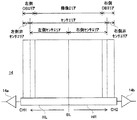
図2を参照して、CCDイメージャ14の撮像面は、複数の受光素子が配置されたセンサエリア(光電変換エリア)と受光素子が配置されていない左側非センサエリアおよび右側非センサエリアとを有する。撮像エリアは、センサエリアのうち水平方向両端の数画素を除くエリアによって形成される。左側OB(Optical Black)エリアは、センサエリアの左端の数画素と左側非センサエリアとによって形成される。右側OBエリアは、センサエリアの右端の数画素と右側非センサエリアとによって形成される。なお、左側OBエリアおよび右側OBエリアは、互いに同じ面積を有する。
Referring to FIG. 2, the imaging surface of
センサエリアは、左側センサエリアおよび右側センサエリアを有する。左側センサエリアは、撮像面の中心から垂直方向に伸びる境界線BLの左側に形成され、右側センサエリアは、同じ境界線BLの右側に形成される。したがって、左側センサエリアおよび右側センサエリアは、境界線BLで互いに接する。左側センサエリアおよび右側センサエリアの各々には、図示しない複数の垂直転送レジスタが割り当てられる。なお、垂直転送レジスタは、左側非センサエリアおよび右側非センサエリアにも割り当てられる。 The sensor area has a left sensor area and a right sensor area. The left sensor area is formed on the left side of the boundary line BL extending in the vertical direction from the center of the imaging surface, and the right sensor area is formed on the right side of the same boundary line BL. Therefore, the left sensor area and the right sensor area are in contact with each other at the boundary line BL. A plurality of vertical transfer registers (not shown) are allocated to each of the left sensor area and the right sensor area. The vertical transfer register is also assigned to the left non-sensor area and the right non-sensor area.
境界線BLの左側に配置された垂直転送レジスタの終端には、水平転送レジスタHLが接続される。また、境界線BLの右側に配置された垂直転送レジスタの終端には、水平転送レジスタHRが接続される。したがって、左側センサエリア上の複数の受光素子で生成された電荷は、図示しない垂直転送レジスタと水平転送レジスタHLとによって転送された後、アンプ14aから出力される。右側センサエリア上の複数の受光素子で生成された電荷も同様に、図示しない垂直転送レジスタと水平転送レジスタHRとによって転送された後、アンプ14bから出力される。
The horizontal transfer register HL is connected to the end of the vertical transfer register arranged on the left side of the boundary line BL. A horizontal transfer register HR is connected to the end of the vertical transfer register arranged on the right side of the boundary line BL. Therefore, the charges generated by the plurality of light receiving elements on the left sensor area are transferred by the vertical transfer register (not shown) and the horizontal transfer register HL, and then output from the
つまり、ドライバ16aは、TG18からのタイミング信号に基づいて左側センサエリアにラスタ走査を施し、左側1/2フレームの生画像信号をチャネルCH1から出力する。ドライバ16bも同様に、TG18からのタイミング信号に基づいて右側センサエリアにラスタ走査を施し、右側1/2フレームの生画像信号をチャネルCH2から出力する。
That is, the
ただし、水平転送レジスタHRの転送方向は、水平転送レジスタHLの転送方向と逆の方向である。このため、ラスタ走査方向もまた、左側センサエリアおよび右側センサエリアの間で互いに反転する。 However, the transfer direction of the horizontal transfer register HR is opposite to the transfer direction of the horizontal transfer register HL. For this reason, the raster scanning direction is also reversed between the left sensor area and the right sensor area.
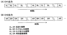
この結果、チャネルCH1の出力は図3(A)に示す要領で変化し、チャネルCH2の出力は図3(B)に示す要領で変化する。図3(A)によれば、期間AL,BL,CLおよびDLがこの順序で繰り返し現れ、図3(B)によれば、期間AR,BR,CRおよびDRがこの順序で繰り返し現れる。このうち、期間ALおよびARの各々は、ラスタ走査に起因する空送り期間であり、期間BLおよびBRの各々は、OBエリアを形成する非センサエリアに対応する期間である。また、期間CLおよびCRの各々は、OBエリアを形成する一部のセンサエリアに対応する期間であり、期間CLおよびCRの各々は、撮像エリアを形成する他の一部のセンサエリアに対応する期間である。 As a result, the output of the channel CH1 changes as shown in FIG. 3A, and the output of the channel CH2 changes as shown in FIG. 3B. According to FIG. 3 (A), periods AL, BL, CL and DL appear repeatedly in this order, and according to FIG. 3 (B), periods AR, BR, CR and DR appear repeatedly in this order. Of these, each of the periods AL and AR is an idle feed period resulting from raster scanning, and each of the periods BL and BR is a period corresponding to a non-sensor area forming the OB area. Each of the periods CL and CR is a period corresponding to a part of the sensor area that forms the OB area, and each of the periods CL and CR corresponds to another part of the sensor area that forms the imaging area. It is a period.
したがって、チャネルCH1の生画像信号は、期間ALにおいて空送りレベルVALを示し、期間BLにおいて光学的黒レベルVBLを示し、期間CLにおいて光学的黒レベルVCLを示し、そして期間DLにおいて有効画像レベルVDLを示す。同様に、チャネルCH2の生画像信号は、期間ARにおいて空送りレベルVARを示し、期間BRにおいて光学的黒レベルVBRを示し、期間CRにおいて光学的黒レベルVCRを示し、そして期間DRにおいて有効画像レベルVDRを示す。 Accordingly, the raw image signal of the channel CH1 indicates the idle feed level VAL in the period AL, the optical black level VBL in the period BL, the optical black level VCL in the period CL, and the effective image level VDL in the period DL. Indicates. Similarly, the raw image signal of the channel CH2 indicates the idle feed level VAR in the period AR, the optical black level VBR in the period BR, the optical black level VCR in the period CR, and the effective image level in the period DR. VDR is shown.
図4を参照して、空送りレベルVALは、アンプ14aで発生したノイズを含み、空送りレベルVARは、アンプ14bで発生したノイズを含む。光学的黒レベルVBLは、左側非センサエリアに割り当てられた垂直転送レジスタと水平転送レジスタHLとで発生したノイズをさらに含み、光学的黒レベルVBRは、右側非センサエリアに割り当てられた垂直転送レジスタと水平転送レジスタHRとで発生したノイズをさらに含む。光学的黒レベルVCLは受光素子で発生したノイズをさらに含み、光学的黒レベルVCRは受光素子で発生したノイズをさらに含む。
Referring to FIG. 4, the idle feed level VAL includes noise generated in the
CCDイメージャ14の撮像面(受光素子,垂直転送レジスタ)で発生するノイズは、場所によって格段に相違することはない。水平転送レジスタHLおよびHRの各々で発生するノイズについても、格段に大きな相違が生じることはない。しかし、アンプ14aおよび14bの各々で生じるノイズについては、増幅特性のばらつきから大きな相違が発生し得る。この結果、図4に示すように、空送りレベルVALおよびVRLが互いに異なる場合がある。
Noise generated on the imaging surface (light receiving element, vertical transfer register) of the
図5を参照して、チャネルCH1の光量−生画像レベル特性は、直線L1によって規定され、チャネルCH2の光量−生画像レベル特性は、直線L2によって規定される。直線L1およびL2の傾きの相違は、アンプ14aおよび14bの増幅率のばらつきに起因する。また、光量がゼロのときのレベル差は“VAL−VAR”となる。
Referring to FIG. 5, the light quantity-raw image level characteristic of channel CH1 is defined by a straight line L1, and the light quantity-raw image level characteristic of channel CH2 is defined by a straight line L2. The difference in the slopes of the straight lines L1 and L2 is caused by variations in the amplification factors of the
図1に戻って、CDS/AGC/AD回路20は、チャネルCH1の生画像信号に相関2重サンプリング,自動ゲイン調整およびA/D変換を施す。同様に、CDS/AGC/AD回路28は、チャネルCH2の生画像信号に相関2重サンプリング,自動ゲイン調整およびA/D変換を施す。なお、CDS/AGC/AD回路20および28の各々も、TG18からのタイミング信号に同期して処理を実行する。
Returning to FIG. 1, the CDS / AGC /
クランプ回路42を形成する加算器22は、CDS/AGC/AD回路20から出力された生画像データとレジスタ26によって保持されたオフセットデータとを入力し、生画像データのデータ値からオフセットデータのデータ値を減算する。同様に、クランプ回路44を形成する加算器30は、CDS/AGC/AD回路28から出力された生画像データとレジスタ34によって保持されたオフセットデータとを入力し、生画像データのデータ値からオフセットデータのデータ値を減算する。加算器22および30の各々から出力される生画像データは、減算されたデータ値を有する。加算器22から出力された生画像データは演算器24のプラス端子に与えられ、加算器30から出力された生画像データは演算器32のプラス端子に与えられる。
The
クランプレベル調整回路36は、クランプレベルデータ(データ値:LV1)を演算器24のマイナス端子に与え、クランプレベルデータ(データ値:LV2)を演算器32のマイナス端子に与える。
The clamp
演算器24は、チャネルCH1の生画像データのデータ値からクランプレベルデータのデータ値LV1を減算する。レジスタ26は、演算器24から出力される減算データのうち、図3(A)に示す期間CLに属する減算データを上述のオフセットデータとして保持する。演算器32もまた、チャネルCH2の生画像データのデータ値からクランプレベルデータのデータ値LV2を減算する。レジスタ34は、演算器32から出力される減算データのうち、図3(B)に示す期間CRに属する減算データを上述のオフセットデータとして保持する。
The
この結果、チャネルCH1の生画像データはデータ値LV1に従うディジタルクランプ処理を施され、チャネルCH2の生画像データはデータ値LV2に従うディジタルクランプ処理を施される。つまり、チャネルCH1の生画像の黒レベルはクランプレベルLV1に設定され、チャネルCH2の生画像の黒レベルはクランプレベルLV2に設定される。 As a result, the raw image data of the channel CH1 is subjected to digital clamping processing according to the data value LV1, and the raw image data of the channel CH2 is subjected to digital clamping processing according to the data value LV2. That is, the black level of the raw image of the channel CH1 is set to the clamp level LV1, and the black level of the raw image of the channel CH2 is set to the clamp level LV2.
信号処理回路38は、加算器22および30の各々から出力された生画像データにチャネルマッチング,色分離,白バランス調整,YUV変換,NTSC符号化の一連の処理を施し、NTSC方式に従うコンポジットビデオ信号を作成する。作成されたコンポジットビデオ信号はLCDモニタ40に与えられる。CCDイメージャ14は30fpsのフレームレートで駆動されるため、滑らかな動きを有する被写界像がLCDモニタ40から出力される。
The
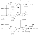
クランプレベル調整回路38は、図6に示すように構成される。CCDイメージャ14から出力されたチャネルCH1の生画像信号は、スイッチSW1およびSW2に与えられる。CCDイメージャ14から出力されたチャネルCH2の生画像信号は、スイッチSW3に与えられる。
The clamp
TG18は、図3(A)に示す期間CLおよびALにスイッチSW1およびSW2をそれぞれオンし、図3(B)に示す期間ARにスイッチSW3をオンする。したがって、チャネルCH1の生画像信号の光学的黒レベルVCLがキャパシタC1によって保持され、チャネルCH1の生画像信号の空送りレベルVALがキャパシタC2によって保持され、そしてチャネルCH2の生画像信号の空送りレベルVARがキャパシタC3によって保持される。
The
キャパシタC1によって保持された光学的黒レベルVCLは、バッファ36aを介して、A/D変換器36fと演算器36dのプラス端子とに与えられる。また、キャパシタC2によって保持された空送りレベルVALは、バッファ36bを介して演算器36dのマイナス端子に与えられる。さらに、キャパシタC3によって保持された空送りレベルVARは、バッファ36cを介して演算器36eのプラス端子に与えられる。
The optical black level VCL held by the capacitor C1 is given to the A /
演算器36dは、光学的黒レベルVCLから空送りレベルVALを減算し、減算レベル“VCL−VAL”を演算器36eの他方のプラス端子に与える。演算器36eは、空送りレベルVARおよび減算レベル“VCL−VAL”を互いに加算し、減算レベル“VCL−(VAL−VAR)”をA/D変換器36gに与える。
The
A/D変換器36fからは、光学的黒レベルVCLに対応するデータ値(=LV1)を有するクランプレベルデータが出力される。また、A/D変換器36gからは、減算レベル“VCL−(VAL−VAR)”に対応するデータ値(=LV2)を有するクランプレベルデータが出力される。そして、かかるクランプレベルデータに従うディジタルクランプ処理が、上述の要領で実行される。この結果、チャネルCH1の光量−生画像レベル特性は、図5に示す直線L1からL1´に遷移する。また、チャネルCH2の光量−生画像レベル特性は、図5に示す直線L2からL2´に遷移する。
The A /
以上の説明から分かるように、CCDイメージャ14は、左側センサエリア(第1光電変換エリア)および右側センサエリア(第2光電変換エリア)が形成された撮像面と、左側センサエリアおよび右側センサエリアにそれぞれ割り当てられた水平転送レジスタHLおよびHRとを有する。左側センサエリアで生成されたチャネルCH1の生画像(第1部分画像)は、ドライバ16a(第1駆動手段)の駆動によってアンプ14aから出力され、右側センサエリアで生成されたチャネルCH2の生画像(第2部分画像)は、ドライバ16b(第2駆動手段)の駆動によってアンプ14bから出力される。
As can be seen from the above description, the
チャネルCH1の生画像は、クランプ回路42(第1クランプ手段)によってクランプレベルLV1(第1クランプレベル)に従うクランプ処理を施される。また、チャネルCH2の生画像は、クランプ回路44(第2クランプ手段)によってクランプレベルLV2(第2クランプレベル)に従うクランプ処理を施される。ここで、クランプレベルLV1は、クランプレベル調整回路36を形成するA/D変換器36f(第1設定手段)によって設定される。また、クランプレベルLV2は、クランプレベル調整回路36を形成するA/D変換器36g(第2設定手段)によって設定される。
The raw image of the channel CH1 is subjected to clamp processing according to the clamp level LV1 (first clamp level) by the clamp circuit 42 (first clamp means). The raw image of the channel CH2 is subjected to a clamping process according to the clamp level LV2 (second clamp level) by the clamp circuit 44 (second clamp means). Here, the clamp level LV1 is set by the A /
クランプレベルLV1は、チャネルCH1の生画像の光学的黒レベルVCLと一致する。一方、クランプレベルLV2は、チャネルCH1の生画像の空送りレベルVALとチャネルCH2の生画像の空送りレベルVARとの差分をチャネルCH1の生画像の黒レベルVCLから減算して求められる減算レベル“VCL−(VAL−VAR)”と一致する。なお、この減算レベル“VCL−(VAL−VAR)”は、演算器36dおよび36e(減算手段)によって算出される。
The clamp level LV1 matches the optical black level VCL of the raw image of the channel CH1. On the other hand, the clamp level LV2 is obtained by subtracting the difference between the blank feed level VAL of the raw image of the channel CH1 and the blank feed level VAR of the raw image of the channel CH2 from the black level VCL of the raw image of the channel CH1. VCL- (VAL-VAR) ". The subtraction level “VCL− (VAL−VAR)” is calculated by the
2つの生画像は互いに異なるチャネルCH1およびCH2からそれぞれ出力されるため、各々の生画像に重畳されるノイズつまり外部ノイズのレベルにずれが生じ得る。 Since the two raw images are output from different channels CH1 and CH2, respectively, the level of noise superimposed on each raw image, that is, the external noise may be generated.
ここで、チャネルCH1の生画像に重畳される外部ノイズのレベルはチャネルCH1の生画像の空送りレベルVALと同一視でき、チャネルCH2の生画像に重畳される外部ノイズのレベルはチャネルCH2の生画像の空送りレベルVARと同一視できる。この結果、空送りレベルVALおよびVARの差分を外部ノイズのずれ量とみなすことができる。 Here, the level of the external noise superimposed on the raw image of the channel CH1 can be identified with the idle feed level VAL of the raw image of the channel CH1, and the level of the external noise superimposed on the raw image of the channel CH2 is the raw level of the channel CH2. The image can be identified with the blank feed level VAR. As a result, the difference between the idle feed levels VAL and VAR can be regarded as a deviation amount of the external noise.
そこで、この実施例では、チャネルCH1の生画像の光学的黒レベルVCLをクランプレベルLV1とする一方、空送りレベルVALおよびVARの差分をチャネルCH1の生画像の光学的黒レベルVCLから減算して求められる減算レベル“VCL−(VAL−VAR)”をクランプレベルLV2としている。これによって、外部ノイズに起因するクランプレベルLV1およびLV2のずれが解消される。 Therefore, in this embodiment, the optical black level VCL of the raw image of the channel CH1 is set to the clamp level LV1, and the difference between the idle feed levels VAL and VAR is subtracted from the optical black level VCL of the raw image of the channel CH1. The required subtraction level “VCL− (VAL−VAR)” is set as the clamp level LV2. This eliminates the shift between the clamp levels LV1 and LV2 due to external noise.
また、クランプレベルLV1およびLV2のいずれも、チャネルCH1の生画像の光学的黒レベルVCLに基づいて設定される。このため、チャネルCH1の生画像の光学的黒レベルVCLとチャネル2の生画像の光学的黒レベルVCRとの相違に起因するクランプレベルLV1およびLV2のずれが解消される。この結果、LCDモニタ40に表示される画像の品質を向上させることができる。
In addition, both of the clamp levels LV1 and LV2 are set based on the optical black level VCL of the raw image of the channel CH1. For this reason, the shift between the clamp levels LV1 and LV2 due to the difference between the optical black level VCL of the raw image of the channel CH1 and the optical black level VCR of the raw image of the
なお、この実施例では、撮像面に形成されたセンサエリアを2つに分割するようにしているが、センサエリアを3つ以上に分割するようにしてもよい。また、この実施例では、左側OBエリアおよび右側OBエリアの面積が互いに同じであるが、この面積は互いに相違してもよい。さらに、この実施例ではディジタルクランプを用いているが、この発明はアナログクランプにも適用できる。 In this embodiment, the sensor area formed on the imaging surface is divided into two, but the sensor area may be divided into three or more. In this embodiment, the areas of the left OB area and the right OB area are the same, but the areas may be different from each other. Further, although the digital clamp is used in this embodiment, the present invention can be applied to an analog clamp.
10 …ディジタルカメラ
14 …CCDイメージャ
22,30 …加算器
24,32 …演算器
26,34 …レジスタ
36 …クランプレベル調整回路
DESCRIPTION OF
Claims (6)
前記第1光電変換エリアで生成された第1部分画像を前記第1出力経路から出力する第1駆動手段、
前記第2光電変換エリアで生成された第2部分画像を前記第2出力経路から出力する第2駆動手段、
前記第1出力経路から出力された第1部分画像に第1クランプレベルに従うクランプ処理を施す第1クランプ手段、
前記第2出力経路から出力された第2部分画像に第2クランプレベルに従うクランプ処理を施す第2クランプ手段、
前記第1出力経路から出力された第1部分画像の黒レベルを前記第1クランプレベルとして設定する第1設定手段、
前記第1出力経路から出力された第1部分画像の空送りレベルから前記第2出力経路から出力された第2部分画像信号の空送りレベルを減算した値を、前記第1出力経路から出力された第1部分画像の黒レベルから減算する減算手段、および
前記減算手段によって求められたレベルを前記第2クランプレベルとして設定する第2設定手段を備える、電子カメラ。 An imaging means having an imaging surface on which a first photoelectric conversion area and a second photoelectric conversion area are formed, and a first output path and a second output path assigned to the first photoelectric conversion area and the second photoelectric conversion area, respectively. ,
First driving means for outputting the first partial image generated in the first photoelectric conversion area from the first output path;
Second driving means for outputting the second partial image generated in the second photoelectric conversion area from the second output path;
First clamping means for applying a clamping process according to a first clamping level to the first partial image output from the first output path;
Second clamping means for applying a clamping process according to a second clamping level to the second partial image output from the second output path;
First setting means for setting a black level of the first partial image output from the first output path as the first clamp level;
The value obtained by subtracting the empty transfer level of the second partial image signal output from the second output path from the preliminary feeding level of the first partial image output from the first output path, output from the first output path An electronic camera comprising: subtracting means for subtracting from the black level of the first partial image; and second setting means for setting the level obtained by the subtracting means as the second clamp level.
前記第1設定手段は前記光学的黒エリアに対応するタイミングで前記黒レベルを検出する黒レベル検出手段を含む、請求項1または2記載の電子カメラ。 The first photoelectric conversion area has an optical black area;
3. The electronic camera according to claim 1, wherein the first setting means includes black level detection means for detecting the black level at a timing corresponding to the optical black area.
前記作成手段は前記静止画像を周期的に作成する、請求項4記載の電子カメラ。 The first driving means and the second driving means periodically output the first partial image and the second partial image, respectively.
The electronic camera according to claim 4, wherein the creation unit periodically creates the still image.
Priority Applications (2)
| Application Number | Priority Date | Filing Date | Title |
|---|---|---|---|
| JP2005030256A JP4636895B2 (en) | 2005-02-07 | 2005-02-07 | Electronic camera |
| US11/347,369 US7609304B2 (en) | 2005-02-07 | 2006-02-06 | CCD camera with a plurality of sensor areas and corresponding output channels correcting image using a clamping process |
Applications Claiming Priority (1)
| Application Number | Priority Date | Filing Date | Title |
|---|---|---|---|
| JP2005030256A JP4636895B2 (en) | 2005-02-07 | 2005-02-07 | Electronic camera |
Publications (3)
| Publication Number | Publication Date |
|---|---|
| JP2006217471A JP2006217471A (en) | 2006-08-17 |
| JP2006217471A5 JP2006217471A5 (en) | 2009-05-07 |
| JP4636895B2 true JP4636895B2 (en) | 2011-02-23 |
Family
ID=36779519
Family Applications (1)
| Application Number | Title | Priority Date | Filing Date |
|---|---|---|---|
| JP2005030256A Expired - Fee Related JP4636895B2 (en) | 2005-02-07 | 2005-02-07 | Electronic camera |
Country Status (2)
| Country | Link |
|---|---|
| US (1) | US7609304B2 (en) |
| JP (1) | JP4636895B2 (en) |
Families Citing this family (10)
| Publication number | Priority date | Publication date | Assignee | Title |
|---|---|---|---|---|
| JP4656115B2 (en) * | 2007-09-27 | 2011-03-23 | ソニー株式会社 | Imaging apparatus, image signal processing circuit, image signal processing method, and computer program |
| JP2009094675A (en) * | 2007-10-05 | 2009-04-30 | Sony Corp | Imaging apparatus, image signal processing circuit, image signal processing method, and computer program |
| JP4743243B2 (en) * | 2008-09-08 | 2011-08-10 | ソニー株式会社 | Imaging apparatus, black level adjusting method and program |
| GB2464453B8 (en) * | 2008-10-10 | 2016-09-14 | Toshiba Res Europ Ltd | An imaging system and method |
| US8378284B2 (en) * | 2009-01-28 | 2013-02-19 | Gentex Corporation | Imaging device |
| US8325248B2 (en) | 2010-06-04 | 2012-12-04 | Apple Inc. | Dual processing of raw image data |
| US8228406B2 (en) | 2010-06-04 | 2012-07-24 | Apple Inc. | Adaptive lens shading correction |
| US8319861B2 (en) | 2010-06-04 | 2012-11-27 | Apple Inc. | Compensation for black level changes |
| EP2420198B1 (en) | 2010-08-19 | 2015-04-08 | Asetronics AG | Hand tool with a lighting device |
| CN104115211B (en) | 2012-02-14 | 2017-09-22 | 金泰克斯公司 | High dynamic range imaging system |
Citations (1)
| Publication number | Priority date | Publication date | Assignee | Title |
|---|---|---|---|---|
| JP2002300477A (en) * | 2001-03-29 | 2002-10-11 | Canon Inc | Signal processing device, signal processing method, and imaging device |
Family Cites Families (6)
| Publication number | Priority date | Publication date | Assignee | Title |
|---|---|---|---|---|
| JPH05227429A (en) * | 1992-02-12 | 1993-09-03 | Ricoh Co Ltd | Signal processing circuit |
| US6205259B1 (en) * | 1992-04-09 | 2001-03-20 | Olympus Optical Co., Ltd. | Image processing apparatus |
| US6337713B1 (en) * | 1997-04-04 | 2002-01-08 | Asahi Kogaku Kogyo Kabushiki Kaisha | Processor for image-pixel signals derived from divided sections of image-sensing area of solid-type image sensor |
| US7245318B2 (en) * | 2001-11-09 | 2007-07-17 | Canon Kabushiki Kaisha | Imaging apparatus that corrects an imbalance in output levels of image data |
| JP3937870B2 (en) | 2002-02-27 | 2007-06-27 | 日本ビクター株式会社 | Imaging device |
| JP3879987B2 (en) * | 2002-04-10 | 2007-02-14 | 日本ビクター株式会社 | Imaging device |
-
2005
- 2005-02-07 JP JP2005030256A patent/JP4636895B2/en not_active Expired - Fee Related
-
2006
- 2006-02-06 US US11/347,369 patent/US7609304B2/en not_active Expired - Fee Related
Patent Citations (1)
| Publication number | Priority date | Publication date | Assignee | Title |
|---|---|---|---|---|
| JP2002300477A (en) * | 2001-03-29 | 2002-10-11 | Canon Inc | Signal processing device, signal processing method, and imaging device |
Also Published As
| Publication number | Publication date |
|---|---|
| US20060176380A1 (en) | 2006-08-10 |
| JP2006217471A (en) | 2006-08-17 |
| US7609304B2 (en) | 2009-10-27 |
Similar Documents
| Publication | Publication Date | Title |
|---|---|---|
| JP4636895B2 (en) | Electronic camera | |
| US5986698A (en) | Image sensing apparatus with a moving image mode and a still image mode | |
| US5648817A (en) | Dual type imaging device having multiple light sensitive elements | |
| JP4803156B2 (en) | SIGNAL PROCESSING DEVICE FOR SOLID-STATE IMAGING ELEMENT, IMAGING DEVICE HAVING SIGNAL PROCESSING DEVICE, SIGNAL PROCESSING METHOD, AND PROGRAM | |
| US7924319B2 (en) | Signal processing apparatus allowing an increase in pixels without an increase in driving frequency and circuit area | |
| US20090201417A1 (en) | Progressive-to-interlace conversion method, image processing apparatus, imaging apparatus | |
| US7443433B2 (en) | Pixel compensating circuit, method for compensating pixels, and image taking apparatus employing such pixel compensating circuit | |
| KR100381496B1 (en) | An image signal processing apparatus | |
| JP2002064831A (en) | Color separation circuit of single plate type color camera | |
| US20090167917A1 (en) | Imaging device | |
| JP4367910B2 (en) | Solid-state imaging device | |
| US20070269133A1 (en) | Image-data noise reduction apparatus and method of controlling same | |
| JP2003101815A (en) | Signal processor and method for processing signal | |
| JP2007214772A (en) | Image signal processing apparatus | |
| US6686961B1 (en) | Image pickup apparatus | |
| JP2005175682A (en) | Imaging apparatus | |
| JPH0470827B2 (en) | ||
| JP4899688B2 (en) | Imaging apparatus and smear false color reduction method thereof | |
| JP4245373B2 (en) | Pixel signal processing circuit | |
| JP2005064760A (en) | Detector and control method for the same | |
| JP2007214770A (en) | Image signal processing apparatus | |
| JPH10174002A (en) | Imaging device | |
| JP2890573B2 (en) | Imaging device | |
| JPH054878B2 (en) | ||
| JP2011101170A (en) | Smear correction method of ccd type solid-state imaging element, and imaging device |
Legal Events
| Date | Code | Title | Description |
|---|---|---|---|
| A621 | Written request for application examination |
Free format text: JAPANESE INTERMEDIATE CODE: A621 Effective date: 20080121 |
|
| A521 | Request for written amendment filed |
Free format text: JAPANESE INTERMEDIATE CODE: A523 Effective date: 20090324 |
|
| A977 | Report on retrieval |
Free format text: JAPANESE INTERMEDIATE CODE: A971007 Effective date: 20091119 |
|
| A131 | Notification of reasons for refusal |
Free format text: JAPANESE INTERMEDIATE CODE: A131 Effective date: 20091124 |
|
| A521 | Request for written amendment filed |
Free format text: JAPANESE INTERMEDIATE CODE: A523 Effective date: 20100120 |
|
| A131 | Notification of reasons for refusal |
Free format text: JAPANESE INTERMEDIATE CODE: A131 Effective date: 20100330 |
|
| TRDD | Decision of grant or rejection written | ||
| A01 | Written decision to grant a patent or to grant a registration (utility model) |
Free format text: JAPANESE INTERMEDIATE CODE: A01 Effective date: 20101026 |
|
| A01 | Written decision to grant a patent or to grant a registration (utility model) |
Free format text: JAPANESE INTERMEDIATE CODE: A01 |
|
| A61 | First payment of annual fees (during grant procedure) |
Free format text: JAPANESE INTERMEDIATE CODE: A61 Effective date: 20101122 |
|
| FPAY | Renewal fee payment (event date is renewal date of database) |
Free format text: PAYMENT UNTIL: 20131203 Year of fee payment: 3 |
|
| FPAY | Renewal fee payment (event date is renewal date of database) |
Free format text: PAYMENT UNTIL: 20131203 Year of fee payment: 3 |
|
| FPAY | Renewal fee payment (event date is renewal date of database) |
Free format text: PAYMENT UNTIL: 20131203 Year of fee payment: 3 |
|
| S111 | Request for change of ownership or part of ownership |
Free format text: JAPANESE INTERMEDIATE CODE: R313113 |
|
| FPAY | Renewal fee payment (event date is renewal date of database) |
Free format text: PAYMENT UNTIL: 20131203 Year of fee payment: 3 |
|
| R350 | Written notification of registration of transfer |
Free format text: JAPANESE INTERMEDIATE CODE: R350 |
|
| LAPS | Cancellation because of no payment of annual fees |