JP4635584B2 - Switching power supply - Google Patents
Switching power supply Download PDFInfo
- Publication number
- JP4635584B2 JP4635584B2 JP2004347863A JP2004347863A JP4635584B2 JP 4635584 B2 JP4635584 B2 JP 4635584B2 JP 2004347863 A JP2004347863 A JP 2004347863A JP 2004347863 A JP2004347863 A JP 2004347863A JP 4635584 B2 JP4635584 B2 JP 4635584B2
- Authority
- JP
- Japan
- Prior art keywords
- switching
- circuit
- switching elements
- capacitor
- power supply
- Prior art date
- Legal status (The legal status is an assumption and is not a legal conclusion. Google has not performed a legal analysis and makes no representation as to the accuracy of the status listed.)
- Expired - Fee Related
Links
Images


Landscapes
- Dc-Dc Converters (AREA)
Description
本発明は、位相シフト方式によるフルブリッジ型のスイッチング電源装置に関する。 The present invention relates to a full-bridge type switching power supply device using a phase shift method.
従来より、スイッチング電源装置として種々のタイプのものが提案され、実用に供されている。そのうちの1つとして、いわゆる位相シフト方式によるフルブリッジ型のスイッチング電源装置が挙げられる。 Conventionally, various types of switching power supply devices have been proposed and put into practical use. One of them is a full-bridge type switching power supply device using a so-called phase shift method.
この位相シフト方式によるフルブリッジ型のスイッチング電源装置では、スイッチング回路としてブリッジ接続された4つのスイッチング素子を含み、これらのスイッチング素子によって、直流入力電圧が交流電圧に変換される。そしてこの交流電圧がトランスによって変圧され、さらに出力回路によって整流および平滑化されることで、直流出力電圧が出力される。 The full-bridge type switching power supply device by this phase shift system includes four switching elements bridge-connected as a switching circuit, and a DC input voltage is converted into an AC voltage by these switching elements. The AC voltage is transformed by a transformer, and further rectified and smoothed by an output circuit to output a DC output voltage.
また、これらのスイッチング素子は、すべて同一のオン幅および周波数で駆動されるが、そのタイミングについてみると2つのスイッチング素子対に区分される。一方のスイッチング素子対を構成する2つのスイッチング素子はともに、時間軸上における固定タイミングでオンするように制御される。他方のスイッチング素子対を構成する2つのスイッチング素子はともに、時間軸上における可変タイミングでオンするように制御される。これら2対のスイッチング素子によるスイッチング動作によって、トランスの1次側巻線に流れる電流が双方向に切り替わり、トランスが励磁される。ここで、これら4つのスイッチング素子による2対の組み合わせは、スイッチング動作のいかなる場面においても、直流入力電圧が印加された入力端子が電気的に短絡されないように設定される。また、固定タイミングでオンするように制御されるスイッチング素子対と、可変タイミングでオンするように制御されるスイッチング素子対との間に生じるスイッチング位相差が、検出した出力電圧等に基づいて制御され、出力電圧が安定化されるようになっている。 These switching elements are all driven with the same ON width and frequency, but are divided into two switching element pairs in terms of the timing. The two switching elements constituting one switching element pair are both controlled to be turned on at a fixed timing on the time axis. The two switching elements constituting the other switching element pair are both controlled to turn on at variable timing on the time axis. By the switching operation by these two pairs of switching elements, the current flowing in the primary winding of the transformer is switched in both directions, and the transformer is excited. Here, the two pairs of combinations of these four switching elements are set so that the input terminal to which the DC input voltage is applied is not electrically short-circuited in any scene of the switching operation. In addition, the switching phase difference generated between the switching element pair controlled to be turned on at a fixed timing and the switching element pair controlled to be turned on at a variable timing is controlled based on the detected output voltage or the like. The output voltage is stabilized.
さらに、これら4つのスイッチング素子にはコンデンサが並列接続されており、これらのコンデンサとトランスのリーケージインダクタンスとにより共振回路が構成され、その共振特性を利用することでゼロボルトスイッチング(ZVS;Zero Volt Switching)動作が実現され、スイッチング素子の短絡損失が低減されるようになっている。 Furthermore, capacitors are connected in parallel to these four switching elements, and a resonance circuit is configured by these capacitors and the leakage inductance of the transformer, and zero volt switching (ZVS) is achieved by utilizing the resonance characteristics. The operation is realized and the short-circuit loss of the switching element is reduced.
例えば、本出願人は特許文献1において、共振回路を構成するインダクタンスとして、トランスのリーケージインダクタンスに加えて独立したインダクタを設け、その共振特性を調整するようにした位相シフト方式によるフルブリッジ型のスイッチング電源装置を提案している。この構成によれば、より確実にZVS動作を実現し、スイッチング素子の短絡損失を低減させることができる。 For example, in Japanese Patent Application Laid-Open No. H10-228867, the present applicant provides a full bridge type switching by a phase shift method in which an independent inductor is provided in addition to the leakage inductance of the transformer as the inductance constituting the resonance circuit, and its resonance characteristics are adjusted. A power supply is proposed. According to this configuration, the ZVS operation can be realized more reliably, and the short-circuit loss of the switching element can be reduced.
しかしながら、上記特許文献1のスイッチング電源装置では、主に定格負荷領域(例えば、出力電流が65〜85A程度の領域)での動作を対象としており、それよりも軽負荷の領域(例えば、出力電流が20A程度の領域)では、共振回路のインダクタに蓄積されるエネルギーが小さくなるため、ドレイン−ソース間電圧を下げることができず、スイッチング素子のターンオン時に大きな短絡損失が発生してしまうという問題がある。このような軽負荷領域での効率低下は、例えば軽負荷領域での高効率化が要求されるハイブリッド自動車等におけるスイッチング電源装置の適用を困難なものとしてしまい、改善の余地があった。
However, the switching power supply device disclosed in
なお、同文献では、負荷の大きさに応じて、共振回路のインダクタンスを変化させる技術についても提案されている。しかしながら、同文献の図24に示されているように、共振回路のインダクタンスを可変のものとすることで全体的に効率が向上してはいるが、依然として軽負荷領域では、定格負荷領域と比べて効率が低下してしまっている。 In the same document, a technique for changing the inductance of the resonance circuit in accordance with the size of the load is also proposed. However, as shown in FIG. 24 of the same document, the overall efficiency is improved by making the inductance of the resonance circuit variable. However, in the light load region, compared with the rated load region. Efficiency has been reduced.
このように、従来の技術では、定格負荷領域における高効率を維持しつつ、それよりも負荷の小さい軽負荷領域においても高効率化が可能なスイッチング電源装置を得るのは困難であり、改善の余地があった。 As described above, in the conventional technology, it is difficult to obtain a switching power supply device that can maintain high efficiency in the rated load region and can achieve high efficiency in a light load region where the load is smaller than that. There was room.
本発明はかかる問題点に鑑みてなされたもので、その目的は、定格負荷領域における高効率を維持しつつ、それよりも負荷の小さい軽負荷領域においても高効率化が可能なスイッチング電源装置を提供することにある。 The present invention has been made in view of such a problem, and an object of the present invention is to provide a switching power supply device that can maintain high efficiency in a rated load region and increase efficiency even in a light load region with a smaller load. It is to provide.
本発明のスイッチング電源装置は、第1ないし第4のスイッチング素子を含み、第1および第2のスイッチング素子の一端同士が互いに接続されて第1の接続点を構成すると共に第3および第4のスイッチング素子の一端同士が互いに接続されて第2の接続点を構成し、第1および第3のスイッチング素子の他端同士と第2および第4のスイッチング素子の他端同士との間に印加される直流入力電圧を交流電圧に変換するスイッチング回路と、第1および第2のスイッチング素子のうちの少なくとも一方と並列に外付け接続された第1の容量素子と、1次側入力および2次側出力を有すると共にこの1次側入力が第1の接続点と第2の接続点との間に接続され、上記交流電圧を変圧するトランスと、第1の接続点からトランスの1次側入力を経由して第2の接続点に至る経路内に挿入され、第1の容量素子と共にZVS動作を行うための共振回路を構成するインダクタと、トランスの2次側出力と接続され、トランスによって変圧された交流電圧に基づいて直流出力電圧を生成する出力回路と、第1および第4のスイッチング素子、または第2および第3のスイッチング素子に対してそれぞれ、固定側スイッチング素子としての第1および第2のスイッチング素子を基準として、シフト側スイッチング素子としての第4および第3のスイッチング素子との間にスイッチング位相差をなすように、これらのスイッチング素子を位相シフト制御により駆動するスイッチング駆動回路と、出力回路の負荷の大きさに応じて、第1の容量素子のうちの少なくとも1つの容量値が変化するように制御する容量素子制御回路とを備えたものである。 The switching power supply device of the present invention includes first to fourth switching elements, one end of each of the first and second switching elements is connected to each other to form a first connection point, and the third and fourth switching elements. One ends of the switching elements are connected to each other to form a second connection point, and are applied between the other ends of the first and third switching elements and the other ends of the second and fourth switching elements. A switching circuit for converting a DC input voltage to an AC voltage, a first capacitive element externally connected in parallel with at least one of the first and second switching elements, a primary input, and a secondary side The transformer has an output and the primary side input is connected between the first connection point and the second connection point, and transforms the alternating voltage, and the primary side input of the transformer from the first connection point. Is inserted in the path leading to the second connection point by reason, an inductor constituting a resonant circuit for ZVS operation with the first capacitive element is connected to the secondary output of the transformer is transformed by the transformer The first and second fixed-side switching elements for the output circuit that generates a DC output voltage based on the AC voltage and the first and fourth switching elements or the second and third switching elements, respectively. A switching drive circuit for driving these switching elements by phase shift control so as to form a switching phase difference between the fourth and third switching elements as the shift-side switching elements with reference to the switching elements of depending on the magnitude of the load of the circuit, so that at least one capacitance value of the first capacitive element is changed Is obtained by a capacitance element control circuit for controlling.
ここで、「外付け接続」とは、容量素子を例えば第1ないし第4のスイッチング素子の寄生容量のみにより構成するのではないことを意味する。また、「スイッチング位相差」とは、スイッチング素子がオン状態となる駆動信号相互間のタイミング差を意味するものである。 Here, “external connection” means that the capacitive element is not configured only by the parasitic capacitances of the first to fourth switching elements, for example. Further, the “switching phase difference” means a timing difference between drive signals at which the switching elements are turned on.
本発明のスイッチング電源装置では、第1ないし第4のスイッチング素子を含むスイッチング回路によって直流入力電圧が交流電圧に変換され、この交流電圧がトランスによって変圧され、この変圧された交流電圧に基づいて、出力回路により直流出力電圧が生成される。第1ないし第4のスイッチング素子は、スイッチング駆動回路によって所定のスイッチング位相差をなすように位相シフト制御により駆動され、上記第1の容量素子およびインダクタが構成する共振回路によるZVS動作によって、スイッチング位相差をなすスイッチング素子の短絡損失が抑制される。また、容量素子制御回路によって、この第1の容量素子のうちの少なくとも1つの容量値が、出力回路の負荷の大きさに応じて変化するようになされる。すなわち、出力回路の負荷の大きさに応じて、共振回路の特性が適切なものとなるように設定される。 In the switching power supply device of the present invention, the DC input voltage is converted into an AC voltage by the switching circuit including the first to fourth switching elements, the AC voltage is transformed by the transformer, and based on the transformed AC voltage, A DC output voltage is generated by the output circuit. The first to fourth switching elements are driven by the phase shift control so as to form a predetermined switching phase difference by the switching drive circuit, and the switching level is changed by the ZVS operation by the resonance circuit formed by the first capacitive element and the inductor. Short-circuit loss of switching elements that make a phase difference is suppressed. Also, the capacitance element control circuit changes the capacitance value of at least one of the first capacitance elements in accordance with the load size of the output circuit. That is, the characteristic of the resonance circuit is set to be appropriate according to the load of the output circuit.
本発明のスイッチング電源装置では、第3および第4のスイッチング素子のうちの少なくとも一方と並列に外付け接続された第2の容量素子を更に設けると共に、容量素子制御回路が、第1および第2の容量素子のうち、第1の容量素子における容量値のみが変化するように制御するのが好ましい。 In the switching power supply device of the present invention, a second capacitive element externally connected in parallel with at least one of the third and fourth switching elements is further provided, and the capacitive element control circuit includes the first and second capacitive elements. Of these capacitive elements, it is preferable to control so that only the capacitance value of the first capacitive element changes.
本発明のスイッチング電源装置では、第1ないし第4のスイッチング素子がそれぞれ寄生容量を有し、容量素子制御回路が、第1の容量素子とこの第1の容量素子に並列接続されたスイッチング素子との間の接続をオン・オフ制御することによって、第1の容量素子の容量値が変化するように制御するように構成することが可能である。 In the switching power supply device of the present invention, each of the first to fourth switching elements has a parasitic capacitance, and the capacitive element control circuit includes a first capacitive element and a switching element connected in parallel to the first capacitive element, It is possible to control so that the capacitance value of the first capacitor element changes by ON / OFF control of the connection between the two.
本発明のスイッチング電源装置では、容量素子制御回路が、出力回路の負荷が小さくなるに応じて、第1の容量素子のうちの少なくとも1つの容量値が小さくなるように制御するように構成することが好ましい。 In the switching power supply device of the present invention, the capacitive element control circuit is configured to control so that the capacitance value of at least one of the first capacitive elements becomes smaller as the load on the output circuit becomes smaller. Is preferred.
本発明のスイッチング電源装置では、第1の容量素子のうちの少なくとも1つが、互いに並列接続された複数のコンデンサから構成され、容量素子制御回路が、これら複数のコンデンサを用いて第1の容量素子の容量値が変化するように制御するように構成することが可能である。またこの場合において、容量素子制御回路が、これら複数のコンデンサのそれぞれの接続を選択的にオン・オフ制御することによって、容量素子の容量値が変化するように制御するように構成することが可能である。 In the switching power supply device of the present invention, at least one of the first capacitive elements includes a plurality of capacitors connected in parallel to each other, and the capacitive element control circuit uses the plurality of capacitors to form the first capacitive element. It is possible to configure so as to control the capacitance value to change. In this case, the capacitive element control circuit can be configured to control the capacitance value of the capacitive element to change by selectively turning on / off each of the plurality of capacitors. It is.
本発明のスイッチング電源装置によれば、共振回路によってスイッチング位相差をなすスイッチング素子の短絡損失を抑制すると共に、容量素子制御回路によって、この共振回路を構成する第1の容量素子のうちの少なくとも1つの容量値を、出力回路の負荷の大きさに応じて変化させるようにしたので、出力回路の負荷の大きさに応じて共振回路の特性を適切なものとすることができ、定格負荷領域における高効率を維持しつつ、軽負荷領域を含む広範な領域において高効率化を図ることが可能となる。
また、第1の容量素子が、第1および第2のスイッチング素子のうちの少なくとも一方と並列に外付け接続されているようにしたので、第3および第4のスイッチング素子側にコンデンサを接続した場合と比べて、特に軽負荷の領域(例えば、出力電流が10A未満の領域)における効率をより向上させることが可能となる。
According to the switching power supply device of the present invention, the short-circuit loss of the switching element having a switching phase difference by the resonance circuit is suppressed, and at least one of the first capacitor elements constituting the resonance circuit is controlled by the capacitor element control circuit. Since one capacitance value is changed according to the load size of the output circuit, the characteristic of the resonance circuit can be made appropriate according to the load size of the output circuit, and in the rated load region While maintaining high efficiency, it is possible to achieve high efficiency in a wide area including a light load area.
Further, since the first capacitive element is externally connected in parallel with at least one of the first and second switching elements, a capacitor is connected to the third and fourth switching elements. Compared to the case, the efficiency can be further improved particularly in a light load region (for example, a region where the output current is less than 10 A).
以下、本発明を実施するための最良の形態(以下、単に実施の形態という。)について、図面を参照して詳細に説明する。 Hereinafter, the best mode for carrying out the present invention (hereinafter simply referred to as an embodiment) will be described in detail with reference to the drawings.
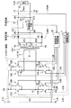
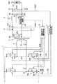
図1は、本発明の一実施の形態に係るスイッチング電源装置の構成を表すものである。このスイッチング電源装置は、図示しない高圧側電源から供給される高圧の直流入力電圧Vinを変換し、より低い直流出力電圧Voutを出力するDC−DCコンバータとして機能するものであり、後述するように位相シフト方式によるフルブリッジ型のスイッチング電源装置である。 FIG. 1 shows a configuration of a switching power supply apparatus according to an embodiment of the present invention. This switching power supply device functions as a DC-DC converter that converts a high-voltage DC input voltage Vin supplied from a high-voltage power supply (not shown) and outputs a lower DC output voltage Vout. This is a full-bridge type switching power supply by a shift method.
このスイッチング電源装置は、1次側高圧ラインL1Hと1次側低圧ラインL1Lとの間に設けられたスイッチング回路1と、インダクタ2と、1次側巻線31および2次側巻線32,33を有し、その1次側巻線31の一端がインダクタ2を介してスイッチング回路1に接続されたトランス3とを備えている。1次側高圧ラインL1Hの入力端子T1と1次側低圧ラインL1Lの入力端子T2との間には、図示しない高圧側電源から直流入力電圧Vinが印加されるようになっている。このスイッチング電源装置はまた、トランス3の2次側に設けられた整流回路4と、この整流回路4に接続された平滑回路5と、この平滑回路5とトランス3との間に配置された電流検出回路61と、この電流検出回路61に接続された容量素子制御回路62と、平滑回路5に接続されたスイッチング駆動回路7とを備えている。なお、上記の高圧側電源は、高圧バッテリであってもよいし、あるいは交流発電機と整流回路との組み合わせであってもよいし、さらに、それらの組み合わせであってもよい。
This switching power supply device includes a
スイッチング回路1は、スイッチング素子S1A〜S4Aと、これらスイッチング素子S1A〜S4Aのそれぞれと並列に外付け接続されたコンデンサC1〜C4と、これらコンデンサC1〜C4の接続をそれぞれ切断するコンデンサ切断素子S1B〜S4Bとを有している。これらスイッチング素子S1A〜S4Aは互いにブリッジ接続されており、具体的には、スイッチング素子S1A,S2Aの一端同士が互いに接続されて接続点P1を構成すると共に、スイッチング素子S3A,S4Aの一端同士が互いに接続されて接続点P2を構成している。また、スイッチング素子S1A,S3Aの他端同士が互いに接続されて接続点P3を構成すると共に、スイッチング素子S2A,S4Aの他端同士が互いに接続されて接続点P4を構成し、これら接続点P3,P4は、それぞれ入力端子T1,T2に接続されている。スイッチング回路1はこのような構成により、入力端子T1,T2間に印加される直流入力電圧Vinを交流電圧に変換するようになっている。
The
なお、スイッチング素子S1A〜S4Aはそれぞれ、例えばMOS−FET(Metal Oxide Semiconductor-Field Effect Transistor)などの三端子スイッチ素子により構成され、コンデンサ切断素子S1B〜S4Bはそれぞれ、例えばバイポーラトランジスタやIGBT(Insulated Gate Bipolor Transistor)などのバイポーラ出力のスイッチ素子により構成される。コンデンサ切断素子S1B〜S4Bをバイポーラ出力のスイッチ素子により構成するのは、電流を双方向に流すことができ、またオフ状態としたときに電流を完全に遮断することができるからである。 The switching elements S1A to S4A are each composed of a three-terminal switch element such as a MOS-FET (Metal Oxide Semiconductor-Field Effect Transistor), and the capacitor disconnecting elements S1B to S4B are each a bipolar transistor or an IGBT (Insulated Gate), for example. Bipolar output switch elements such as bipolar transistors). The reason why the capacitor disconnecting elements S1B to S4B are constituted by bipolar output switch elements is that current can flow in both directions, and that the current can be completely cut off when turned off.
インダクタ2は、その一端がスイッチング素子S3A,S4Aの一端同士と接続点P2で接続され、その他端がトランス3の1次側巻線31の一端に接続されている。このインダクタ2は、スイッチング回路1内のコンデンサC1〜C4と共に共振回路を構成し、この共振回路による共振特性を利用することで、後述するようにスイッチング素子S1A〜S4Aにおける短絡損失を抑制するようになっている。なお、このインダクタ2の配置はこの位置には限られず、接続点P1からトランスの1次側巻線31を経由して接続点P2に至る経路内に挿入されていればよい。また、このインダクタ2の代わりに、もしくはインダクタ2に加えて、トランス3における1次側巻線31のリーケージインダクタンス(図示せず)を用いて共振回路を構成するようにしてもよい。
One end of the
トランス3の1次側巻線31は、その一端がインダクタ2の他端に接続され、その他端がスイッチング素子S1A,S2Aの一端同士と接続点P1で接続されている。また、2次側巻線32,33の一端はそれぞれ接続点P7(センタタップ)で互いに接続され、それらの他端はそれぞれ、ダイオード41,42のアノードと接続点P5,P6で接続されている。また、接続点P7(センタタップ)は接地ラインLGおよび電流検出回路61を介して出力端子T4に導かれている。つまり、このスイッチング電源装置はセンタタップ型のものである。このトランス3は、スイッチング回路1によって変換された交流電圧を降圧し、一対の2次側巻線32,33の他端(接続点P5,P6)から、互いに180度位相が異なる交流電圧VO1,VO2を出力するようになっている。なお、この場合の降圧の度合いは、1次側巻線31と2次側巻線32,33との巻数比によって定まる。
One end of the primary winding 31 of the
整流回路4は、一対のダイオード41,42から構成される両波整流型のものである。ダイオード41のアノードは、2次側巻線32の他端と接続点P5で接続され、ダイオード42のアノードは、2次側巻線33の他端と接続点P6で接続されている。また、これらダイオード41,42のカソード同士は、接続点P8で互いに接続されると共に、出力ラインLOに接続されている。つまり、この整流回路4はカソードコモン接続の構造を有しており、トランス3の交流出力電圧VO1,VO2の各半波期間をそれぞれダイオード41,42によって個別に整流して直流電圧を得るようになっている。
The
平滑回路5は、チョークコイル51と平滑コンデンサ52とを含んで構成されている。チョークコイル51は、出力ラインLOに挿入配置されており、その一端はダイオード41,42のカソード同士と接続点P8で接続され、その他端は平滑コンデンサ52の一端および出力ラインLOの出力端子T3と接続点P9で接続されている。平滑コンデンサ52は、出力ラインLO(具体的には、接続点P9)と接地ラインLG(具体的には、接続点P10)との間に接続されている。出力ラインLOの端部には、出力端子T4が設けられている。平滑回路5はこのような構成により、整流回路4で整流された直流電圧を平滑化して直流出力電圧Voutを生成し、これを出力端子T3,T4から負荷8へ供給するようになっている。
The smoothing
電流検出回路61は、接地ラインLGに挿入配置(具体的には、接続点P7,10の間に配置)されて、出力電流Ioutに対応する信号LIoutを出力するようになっている。なお、1次側巻線31に流れる電流は出力電流Ioutに比例しているので、図1の構成とは異なり、電流検出回路61を、接続点P1からインダクタ2および1次側巻線31を介して接続点P2に至る経路内に挿入配置するようにしてもよい。また、図1の構成とは異なり、電流検出回路61を、図示しない高圧側電源からスイッチング回路1に流れる電流を検出するように配置してもよい。
The
容量素子制御回路62は、電流検出回路61から出力された信号LIoutに基づいて、スイッチング回路1内のコンデンサC1〜C4の容量値が変化するように制御するものである。具体的には、本実施の形態のスイッチング電源装置では、コンデンサ切断素子S1B〜S4Bに対してそれぞれコンデンサ切断信号L1B〜L4Bを供給し、例えばコンデンサC1〜C4の接続をオン・オフ制御することで、スイッチング素子S1A〜S4Aに並列な容量値が変化するように制御するようになっている。このようにして容量素子制御回路62は、後述するように共振回路の共振特性を負荷8の大きさ(出力電流Ioutの大きさ)に応じて適切に変化させるようになっている。なお、前述のようにスイッチング素子S1A〜S4AをMOS−FETにより構成した場合には、このMOS−FETの寄生容量も、スイッチング素子S1A〜S4Aに並列な容量として利用することができる。
The capacitive
スイッチング駆動回路7は、出力電圧Voutに対応する信号LVout(出力ラインLOの接続点P9から供給される)に基づいて、スイッチング回路1内のスイッチング素子S1A〜S4Aを駆動するものである。具体的には、本実施の形態のスイッチング電源装置では、スイッチング素子S1A〜S4Aに対してそれぞれスイッチング駆動信号L1A〜L4Aを供給し、これらスイッチング素子S1A〜S4Aをオン・オフ制御するようになっている。また、スイッチング駆動回路7は、後述するようにこれらスイッチング素子S1A〜S4Aに対してスイッチング位相制御を行い、スイッチング位相差を適切に設定することで、直流出力電圧Voutを安定化させるようになっている。
The switching
ここで、スイッチング素子S1A〜S4Aはそれぞれ、本発明における「第1ないし第4のスイッチング素子」の一具体例に対応するものであり、コンデンサC1〜C4およびコンデンサ切断素子S1B〜S4Bは、本発明における「容量素子」の一具体例に対応するものである。また、1次側巻線31および2次側巻線32,33はそれぞれ、本発明における「1次側入力」および「2次側出力」の一具体例に対応するものであり、整流回路4および平滑回路5は、本発明における「出力回路」の一具体例に対応するものである。また、接続点P1,P2はそれぞれ、本発明における「第1の接続点」および「第2の接続点」の一具体例に対応するものであり、接続点P3,P4はそれぞれ、本発明における「第1および第3のスイッチング素子の他端同士」ならびに「第2および第4のスイッチング素子の他端同士」の一具体例に対応するものである。
Here, each of the switching elements S1A to S4A corresponds to a specific example of “first to fourth switching elements” in the present invention, and the capacitors C1 to C4 and the capacitor disconnecting elements S1B to S4B correspond to the present invention. Corresponds to a specific example of “capacitance element” in FIG. The primary side winding 31 and the
次に、図2〜図13を参照して、以上のような構成のスイッチング電源装置の動作を、負荷8の大きさ(出力電流Ioutの大きさ)に応じて、定格負荷領域(例えば、出力電流Ioutが50A以上の領域)と、軽負荷領域(例えば、出力電流Ioutが30A未満の領域)と、中間負荷領域(例えば、出力電流Ioutが30A以上50A未満の領域)とに分けて説明する。なお、以下の回路図においては、スイッチング素子S1A〜S4AおよびコンデンサC1〜C4と並列接続されたダイオードD1〜D4についても考慮するものとする。これらダイオードD1〜D4としては、前述のようにスイッチング素子S1A〜S4AをMOS−FETにより構成した場合には、このMOS−FETの寄生ダイオードを利用することができ、寄生ダイオードを持たない他の三端子スイッチ素子により構成した場合には、外付け接続したものを利用する。 Next, referring to FIGS. 2 to 13, the operation of the switching power supply having the above-described configuration is performed according to the size of the load 8 (the magnitude of the output current Iout) (for example, the output load region). An area where the current Iout is 50 A or more), a light load area (for example, an area where the output current Iout is less than 30 A), and an intermediate load area (for example, an area where the output current Iout is 30 A or more and less than 50 A) will be described. . In the following circuit diagram, the switching elements S1A to S4A and the diodes D1 to D4 connected in parallel with the capacitors C1 to C4 are also considered. As the diodes D1 to D4, when the switching elements S1A to S4A are composed of MOS-FETs as described above, parasitic diodes of the MOS-FETs can be used, and other three diodes having no parasitic diodes can be used. When the terminal switch element is used, an externally connected one is used.
まず、定格負荷領域における動作を説明する。 First, the operation in the rated load region will be described.
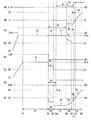
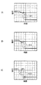
図2は、定格負荷領域におけるスイッチング電源装置の各部の電圧波形を表すもので、(A)はスイッチング駆動信号L1Aの電圧波形を示し、(B)は並列接続されたスイッチング素子S1AとダイオードD1とコンデンサC1とからなる回路に流れる電流I1の波形を実線で、スイッチング素子S1Aの両端間の電圧V1(スイッチング素子S1Aが例えばMOS−FETにより構成されている場合には、ドレイン−ソース間の電圧。以下同様。)の波形を点線で示し、(C)はスイッチング駆動信号L2Aの電圧波形を示し、(D)は並列接続されたスイッチング素子S2AとダイオードD2とコンデンサC2とからなる回路に流れる電流I2の波形を実線で、スイッチング素子S2Aの両端間の電圧V2の波形を点線で示し、(E)はスイッチング駆動信号L3Aの電圧波形を示し、(F)は並列接続されたスイッチング素子S3AとダイオードD3とコンデンサC3とからなる回路に流れる電流I3の波形を実線で、スイッチング素子S3Aの両端間の電圧V3の波形を点線で示し、(G)はスイッチング駆動信号L4Aの電圧波形を示し、(H)は並列接続されたスイッチング素子S4AとダイオードD4とコンデンサC4とからなる回路に流れる電流I4の波形を実線で、スイッチング素子S4Aの両端間の電圧V4の波形を点線で示している。なお、ここに示した例では、電圧V1〜V4の最大値=Vinとする。 2A and 2B show voltage waveforms of respective parts of the switching power supply apparatus in the rated load region. FIG. 2A shows the voltage waveform of the switching drive signal L1A, and FIG. 2B shows switching elements S1A and diodes D1 connected in parallel. The waveform of the current I1 flowing through the circuit composed of the capacitor C1 is a solid line, and the voltage V1 across the switching element S1A (when the switching element S1A is composed of, for example, a MOS-FET, the voltage between the drain and the source. The same applies to the following.) (C) shows the voltage waveform of the switching drive signal L2A, and (D) shows the current I2 flowing through the circuit composed of the switching element S2A, the diode D2, and the capacitor C2 connected in parallel. (E) is indicated by a solid line, and the waveform of the voltage V2 across the switching element S2A is indicated by a dotted line. The voltage waveform of the switching drive signal L3A is shown, and (F) is a solid line showing the waveform of the current I3 flowing through the circuit composed of the switching element S3A, the diode D3, and the capacitor C3 connected in parallel, and the voltage V3 across the switching element S3A. (G) shows the voltage waveform of the switching drive signal L4A, and (H) shows the waveform of the current I4 flowing through the circuit composed of the switching element S4A, the diode D4, and the capacitor C4 connected in parallel. The waveform of the voltage V4 across the switching element S4A is indicated by a dotted line. In the example shown here, the maximum value of the voltages V1 to V4 = Vin.
図1に示したスイッチング電源装置において、ブリッジ接続されたスイッチング素子S1A〜S4Aは、スイッチング制御回路7から供給されるスイッチング駆動信号L1A〜L4Aにより、すべて同一のオン幅および周波数となるように駆動される。そしてこれらスイッチング素子S1A〜S4Aのスイッチング動作により、トランス3の1次側巻線31に流れる電流が双方向に切り替えられ、それによってトランス3が励磁される。トランス3の2次側巻線32,33に生じた交流電圧は、整流回路4によって整流され、平滑回路5によって平滑化されることで、直流出力電圧Voutとして、出力端子T3,T4から負荷8に供給される。
In the switching power supply device shown in FIG. 1, the bridge-connected switching elements S1A to S4A are all driven by the switching drive signals L1A to L4A supplied from the switching
スイッチング素子S1A〜S4Aが駆動されるタイミングについてみると、これらのスイッチング素子は、2つのスイッチング素子対に区分される。具体的には、スイッチング素子S1Aおよびスイッチング素子S2Aははともに、時間軸上における固定タイミングでオンするように制御され、「固定側スイッチング素子」と称される。また、スイッチング素子S3Aおよびスイッチング素子S4Aはともに、時間軸上における可変タイミングでオンするように制御され、「シフト側スイッチング素子」と称される。 Looking at the timing at which the switching elements S1A to S4A are driven, these switching elements are divided into two switching element pairs. Specifically, both the switching element S1A and the switching element S2A are controlled to be turned on at a fixed timing on the time axis, and are referred to as “fixed-side switching elements”. Further, both the switching element S3A and the switching element S4A are controlled to be turned on at a variable timing on the time axis, and are referred to as “shift-side switching elements”.
また、これらスイッチング素子S1A〜S4Aは、スイッチング動作のいかなる状態においても、直流入力電圧Vinが印加された入力端子T1,T2が電気的に短絡されない組み合わせおよびタイミングで駆動される。具体的には、スイッチング素子S1Aおよびスイッチング素子S2A(固定側スイッチング素子)は、同時にオンとなることはない。また、スイッチング素子S3Aおよびスイッチング素子S4A(シフト側スイッチング素子)も、同時にオンとなることはない。これらが同時にオンとなるのを回避するためにとられる時間的間隔は、デッドタイムTdと称される。 Further, these switching elements S1A to S4A are driven with a combination and timing at which the input terminals T1 and T2 to which the DC input voltage Vin is applied are not electrically short-circuited in any state of the switching operation. Specifically, the switching element S1A and the switching element S2A (fixed side switching element) are not simultaneously turned on. Further, the switching element S3A and the switching element S4A (shift-side switching element) are not simultaneously turned on. The time interval taken to avoid turning them on at the same time is called the dead time Td.
スイッチング素子S1Aおよびスイッチング素子S4Aは同時にオンとなる期間を有し、この同時にオンとなる期間において、トランス3の1次側巻線31が励磁される。これらスイッチング素子S1Aおよびスイッチング素子S4Aは、スイッチング素子S1A(固定側スイッチング素子)を基準としてスイッチング位相差φをなすように動作する。これらが同時にオンとなる期間は、このスイッチング位相差φを制御することにより、制御される。
The switching element S1A and the switching element S4A have a period in which they are simultaneously turned on, and the primary winding 31 of the
また同様に、スイッチング素子S2Aおよびスイッチング素子S3Aは同時にオンとなる期間を有し、この同時にオンとなる期間において、トランス3の1次側巻線31が、上記の場合とは逆方向に励磁される。これらスイッチング素子S2Aおよびスイッチング素子S3Aは、スイッチング素子S2A(固定側スイッチング素子)を基準としてスイッチング位相差φをなすように動作する。
Similarly, the switching element S2A and the switching element S3A have a period in which they are simultaneously turned on. During this period in which the switching elements S2A and S3A are simultaneously turned on, the primary winding 31 of the
さらに、出力電圧Voutの制御のために、例えば出力電圧Voutに対応する信号LVoutに基づいて、スイッチング素子S1Aとスイッチング素子S4Aとのスイッチング位相差φ、およびスイッチング素子S2Aとスイッチング素子S3Aとのスイッチング位相差φがそれぞれ制御され、スイッチング素子S1Aおよびスイッチング素子S4Aが同時にオンになっている時間、ならびにスイッチング素子S2Aおよびスイッチング素子S3Aが同時にオンになっている時間が変化する。これにより、トランス3の1次側巻線31に印加される電圧のデューティ比が変化し、出力電圧Voutが安定化される。
Further, for controlling the output voltage Vout, for example, based on the signal LVout corresponding to the output voltage Vout, the switching phase difference φ between the switching element S1A and the switching element S4A, and the switching position between the switching element S2A and the switching element S3A. The phase difference φ is controlled, and the time during which the switching element S1A and the switching element S4A are simultaneously turned on and the time during which the switching element S2A and the switching element S3A are simultaneously turned on vary. As a result, the duty ratio of the voltage applied to the primary winding 31 of the
スイッチング素子S2Aがオフとなってから、スイッチング素子S1AがオンとなるまでのデッドタイムTdの期間中に、スイッチング素子S1Aに並列接続されたコンデンサC1、スイッチング素子S2Aに並列接続されたコンデンサC2、インダクタ2およびトランス3の励磁インダクタンスにより、共振回路が構成される。この共振回路による共振作用を利用して、コンデンサC1に蓄積されていた電荷が全て放出された後にスイッチング素子S1Aをオンにすることにより、ZVS動作を達成でき、コンデンサC1の短絡損失およびそれに伴うノイズの発生が抑制される。スイッチング素子S2Aにおいても同様であり、コンデンサC2に蓄積されていた電荷が全て放出された後にスイッチング素子S2Aをオンにすることにより、ZVS動作を達成でき、コンデンサC2の短絡損失およびそれに伴うノイズの発生が抑制される。
The capacitor C1 connected in parallel to the switching element S1A, the capacitor C2 connected in parallel to the switching element S2A, and the inductor during the dead time Td from when the switching element S2A is turned off to when the switching element S1A is turned on A resonance circuit is configured by the excitation inductance of the
また、スイッチング素子S3Aがオフとなってから、スイッチング素子S4AがオンとなるまでのデッドタイムTdの期間中に、スイッチング素子S3Aに並列接続されたコンデンサC3、スイッチング素子S4Aに並列接続されたコンデンサC4、インダクタ2およびチョークコイル51のインダクタンスをトランス3の1次側に換算したインダクタにより、共振回路が構成される。この共振回路による共振作用を利用して、コンデンサC4に蓄積されていた電荷が全て放出された後にスイッチング素子S4Aをオンにすることにより、ZVS動作を達成でき、コンデンサC4の短絡損失およびそれに伴うノイズの発生が抑制される。スイッチング素子S3Aにおいても同様であり、コンデンサC3に蓄積されていた電荷が全て放出された後にスイッチング素子S3Aをオンにすることにより、ZVS動作を達成でき、コンデンサC3の短絡損失およびそれに伴うノイズの発生が抑制される。
Further, during the dead time Td from when the switching element S3A is turned off to when the switching element S4A is turned on, the capacitor C3 connected in parallel to the switching element S3A and the capacitor C4 connected in parallel to the switching element S4A A resonant circuit is configured by an inductor obtained by converting the inductance of the
なお、スイッチング素子S1A〜S4Aにそれぞれ並列接続されたコンデンサC1〜C4は、電流検出回路61から出力された出力電流Ioutに対応する信号LIoutに基づいて容量素子制御回路により生成されたコンデンサ切断信号L1B〜L4Bによって、その接続がオン・オフ制御される。ただし、定格負荷領域ではこれらコンデンサC1〜C4は常に接続され、インダクタ2と共に共振回路を構成するようになっている。
The capacitors C1 to C4 connected in parallel to the switching elements S1A to S4A are respectively connected to the capacitor disconnection signal L1B generated by the capacitor element control circuit based on the signal LIout corresponding to the output current Iout output from the
ここで、スイッチング電源装置の動作をさらに詳しく説明する。このスイッチング電源装置では、図2に示した各部の電圧電流波形およびスイッチング駆動信号L1A〜L4Aから、回路の動作上、大きく分けて5つのステージ(期間T1〜T5)が考えられる。以下、図2に加えて図3〜図10を参照して、各ステージについて説明する。 Here, the operation of the switching power supply device will be described in more detail. In this switching power supply device, five stages (periods T1 to T5) can be roughly divided from the voltage / current waveform of each part and the switching drive signals L1A to L4A shown in FIG. Hereinafter, each stage will be described with reference to FIGS. 3 to 10 in addition to FIG. 2.
<第1のステージ>
第1のステージは、図2の期間T1に対応する。図3は、図1に示したスイッチング電源装置において、第1のステージで働く回路部分を実線で示したものである。この第1のステージは、スイッチング素子S2Aとスイッチング素子S3Aとがオン状態になり、スイッチング電源装置の入力側から出力側へ電力を伝送している期間である。スイッチング素子S1Aおよびスイッチング素子S4Aはオフ状態にある。ここで、スイッチング素子S2Aとスイッチング素子S3Aとに流れる電流Iaは、出力電流Ioutとトランス3の巻数比とによって定まる。この第1のステージは、スイッチング素子S3Aがターンオフするまで継続する。
<First stage>
The first stage corresponds to the period T1 in FIG. FIG. 3 shows a circuit portion working in the first stage in the switching power supply device shown in FIG. 1 by a solid line. The first stage is a period in which the switching element S2A and the switching element S3A are turned on and power is transmitted from the input side to the output side of the switching power supply device. Switching element S1A and switching element S4A are in an off state. Here, the current Ia flowing through the switching element S2A and the switching element S3A is determined by the output current Iout and the turns ratio of the
<第2のステージ>
第2のステージは、図2の期間T2に対応する。図4は、図1に示したスイッチング電源装置において、第2のステージで働く回路部分を実線で示したものである。第2のステージは、スイッチング素子S3Aに並列接続されたコンデンサC3が充電される(+q3,−q3)と共に、スイッチング素子S4Aに並列接続されたコンデンサC4に蓄積されていた電荷(+q4,−q4)が放電される期間である。第2のステージでは、スイッチング素子S3Aがオフになる。また、スイッチング素子S1Aおよびスイッチング素子S4Aはオフ状態を継続する。このようにスイッチング素子S3Aがオフとなったことで、上記のようにコンデンサC3が充電されると共に、コンデンサC4に蓄積されていた電荷が放電される。第2のステージでは、トランス3が電力伝送を行っているので、コンデンサC3は一定電流Ibで充電され、コンデンサC4の蓄積電荷は一定電流Icで放電される。よって、図2に示したように、スイッチング素子S3Aの両端間の電圧V3およびスイッチング素子S4Aの両端間の電圧V4は、直線的に変化する。この第2のステージは、スイッチング素子S4Aに並列接続されたダイオードD4が導通し、スイッチング素子S3Aの両端間の電圧V3が直流入力電圧Vinによりクランプされるまで継続する。
<Second stage>
The second stage corresponds to the period T2 in FIG. FIG. 4 shows a circuit portion that works in the second stage in the switching power supply device shown in FIG. 1 by a solid line. In the second stage, the capacitor C3 connected in parallel to the switching element S3A is charged (+ q3, −q3), and the charge (+ q4, −q4) accumulated in the capacitor C4 connected in parallel to the switching element S4A. Is the period during which is discharged. In the second stage, the switching element S3A is turned off. Further, the switching element S1A and the switching element S4A continue to be in the off state. Since the switching element S3A is turned off in this way, the capacitor C3 is charged as described above, and the charge accumulated in the capacitor C4 is discharged. In the second stage, since the
<第3のステージ>
第3のステージは、図2の期間T3に対応する。図5および図6は、図1に示したスイッチング電源装置において、第3のステージで働く回路部分を実線で示したものである。第3のステージは、インダクタ2に蓄積されていたエネルギーが、スイッチング素子S4Aに並列接続されたダイオードD4とスイッチング素子S2Aとを通って放出される期間である(図5)。よって、ダイオードD4およびスイッチング素子S2Aに流れる電流Ifはほとんど変化しない。図2に示すように、第3のステージの途中で、スイッチング素子S4Aがターンオンし、ダイオードD4に流れていた電流Ifがスイッチング素子S4Aに流れるようになるが(図6)、基本的な動作状態は変化しない。第3のステージは、スイッチング素子S2Aがターンオフするまで継続する。
<Third stage>
The third stage corresponds to the period T3 in FIG. FIG. 5 and FIG. 6 show, in solid lines, circuit portions that work in the third stage in the switching power supply device shown in FIG. The third stage is a period in which the energy stored in the
<第4のステージ>
第4のステージは、図2の期間T4に対応する。図7は、図1に示したスイッチング電源装置において、第4のステージで働く回路部分を実線で示したものである。第4のステージでは、第2のステージと異なり、トランス3が短絡状態となっているため、スイッチング素子S2Aがターンオフすると、スイッチング素子S1Aに並列接続されたコンデンサC1、スイッチング素子S2Aに並列接続されたコンデンサC2およびインダクタ2が共振する。そのため、図2に示したように、コンデンサC1に流れる電流Ik、スイッチング素子S1Aの両端間の電圧V1、コンデンサC2に流れる電流Ijおよびスイッチング素子S2Aの両端間の電圧V2は、三角関数的に変化する。第4のステージは、スイッチング素子S1Aに並列接続されたダイオードD1が導通するまで継続する。
<Fourth stage>
The fourth stage corresponds to the period T4 in FIG. FIG. 7 shows a circuit portion working in the fourth stage in the switching power supply device shown in FIG. 1 by a solid line. In the fourth stage, unlike the second stage, since the
<第5のステージ>
第5のステージは、図2の期間T5に対応する。図8〜図10は、図1に示したスイッチング電源装置において、第5のステージで働く回路部分を実線で示したものである。第5のステージでは、まず、スイッチング素子S1Aに並列接続されたダイオードD1が導通したことにより、インダクタ2に蓄積されていたエネルギーが、スイッチング素子S4AとダイオードD1とを通って図示しない高圧側電源に回生される(図8)。この第5のステージの途中で、スイッチング素子S1Aがターンオン(図9)するが、基本的な動作状態は変化しない。インダクタ2に流れる電流Isがゼロになると(図2)、インダクタ2に充電電流Iuが流れる(図10)。充電電流Iuは、整流回路4内のダイオード41に流れる電流が出力電流Ioutに等しくなるまで流れ続ける。よって、図2に示したように、この第5のステージにおいて流れる電流は、直線的に変化する。また、インダクタ2に流れる電流Isがゼロになる前にスイッチング素子S1Aもしくはスイッチング素子S2Aをターンオンさせることで、デッドタイムTdの期間中の再共振が防止される。
<5th stage>
The fifth stage corresponds to the period T5 in FIG. 8 to 10 show the circuit portion working in the fifth stage in the switching power supply device shown in FIG. 1 by solid lines. In the fifth stage, first, the diode D1 connected in parallel to the switching element S1A is turned on, so that the energy stored in the
このように、定格負荷領域では、従来のようにスイッチング素子S1A〜S4AにコンデンサC1〜C4を並列接続し、これらコンデンサC1〜C4とインダクタ2とにより適切な共振回路を構成することで、その共振特性を利用してZVS動作が達成され、スイッチング位相制御されるスイッチング素子同士の短絡損失が抑制される。
In this way, in the rated load region, the capacitors C1 to C4 are connected in parallel to the switching elements S1A to S4A as in the prior art, and these capacitors C1 to C4 and the
次に、軽負荷領域における動作を説明する。 Next, the operation in the light load region will be described.
この軽負荷領域では、電流検出回路61によって出力電流Ioutがこの領域の値であることが検出されると、容量素子制御回路62によって、スイッチング素子S1Aに並列接続されたコンデンサC1およびスイッチング素子S2Aに並列接続されたコンデンサC2、すなわち固定側スイッチング素子のコンデンサの接続が切断される。よって、例えば前述の第4のステージ(図7)においては、図11に示したような回路構成となる。なお、図11に示した回路構成では、コンデンサC1,C2の接続が切断されているため、図7に示した回路構成とは異なり、そのままではLC共振回路が成立しなくなってしまう。そこで、前述のように例えばスイッチング素子S1A〜S4AをMOS−FETにより構成した場合には、このMOS−FETの微小な寄生容量を利用し、スイッチング素子S1A〜S4Aを他の素子により構成した場合には、容量の小さいコンデンサを外付け接続して利用するようにする。
In this light load region, when the
このように、固定側スイッチング素子のコンデンサC1,C2の接続を切断することで、共振回路の容量値Cを小さくし、以下の式(1)により、共振回路のインピーダンスZを大きくすることができる。ここで、式(1)中のLは、共振回路のインダクタンスを表している。よって、共振回路のインピーダンスZを大きくすることで、以下の式(2)により、スイッチング素子S2Aの両端間の電圧V4のピーク値V2(peak)を大きくすることができ、またスイッチング素子S1Aの両端間の電圧V1の最小値も小さくすることができる(それぞれ、図12の矢印X1,X2)。なお、式(2)中のnは、トランス3における1次側巻線31と2次側巻線32,33との巻数比を表している。
In this way, by disconnecting the capacitors C1 and C2 of the fixed-side switching element, the capacitance value C of the resonance circuit can be reduced, and the impedance Z of the resonance circuit can be increased by the following equation (1). . Here, L in Formula (1) represents the inductance of the resonant circuit. Therefore, by increasing the impedance Z of the resonance circuit, the peak value V2 (peak) of the voltage V4 across the switching element S2A can be increased by the following equation (2), and both ends of the switching element S1A can be increased. The minimum value of the voltage V1 between them can also be reduced (arrows X1 and X2 in FIG. 12, respectively). Note that n in the expression (2) represents the turn ratio of the primary winding 31 and the
Z={L/(2C)}1/2 …(1)
V2(peak)=n・Iout・Z …(2)
Z = {L / (2C)} 1/2 (1)
V2 (peak) = n · Iout · Z (2)
ここで、図12に示したように、共振回路によるZVS動作をしやすくするためには、以下の式(3)により、このスイッチング素子S4Aの両端間の電圧V4のピーク値V4(peak)を直流入力電圧Vin以上の値にすればよい。したがって、コンデンサC1およびコンデンサC2の接続を切断し、共振回路のインピーダンスZを大きくすることで、共振回路によるZVS動作をしやすくし、定格負荷領域と同様に、軽負荷領域においてもスイッチング素子の短絡損失を抑制することができる。また、たとえZVS動作が達成できなかったとしても、共振回路の容量値Cを小さくしているので、以下の式(4)により、スイッチング素子の短絡損失Plossを小さく抑えることができる。なお、式(4)中のVおよびfはそれぞれ、コンデンサの両端間の電圧、および共振回路の共振周波数を表している。 Here, as shown in FIG. 12, in order to facilitate the ZVS operation by the resonance circuit, the peak value V4 (peak) of the voltage V4 across the switching element S4A is obtained by the following equation (3). What is necessary is just to set it as the value more than DC input voltage Vin. Therefore, by disconnecting the capacitor C1 and the capacitor C2 and increasing the impedance Z of the resonance circuit, the ZVS operation by the resonance circuit is facilitated, and the switching element is short-circuited in the light load region as well as in the rated load region. Loss can be suppressed. Even if the ZVS operation cannot be achieved, since the capacitance value C of the resonant circuit is reduced, the short-circuit loss Ploss of the switching element can be reduced by the following equation (4). Note that V and f in Equation (4) represent the voltage across the capacitor and the resonance frequency of the resonance circuit, respectively.
V2(peak)≧Vin …(3)
Ploss=(1/2)・C・V2・f …(4)
V2 (peak) ≧ Vin (3)
Ploss = (1/2) · C · V 2 · f (4)
最後に、中間負荷領域における動作を説明する。 Finally, the operation in the intermediate load region will be described.
この中間負荷領域では、電流検出回路61によって出力電流Ioutがこの領域の値であることが検出されると、容量素子制御回路62によって、固定側スイッチング素子のコンデンサC1,C2のいずれか一方の接続が切断される。よって、例えばコンデンサC2の接続を切断した場合、例えば前述の第4のステージ(図7)においては、図13に示したような回路構成となる。
In this intermediate load region, when the
前述の軽負荷領域とは異なり、固定側スイッチング素子のコンデンサC1,C2のいずれか一方のみの接続を切断するのは、中間負荷領域では両方のコンデンサの接続を切断すると、以下の式(5)により共振回路の共振角周波数ωが軽負荷領域の場合と比べて高くなりすぎると共に、もともと共振時のエネルギーも軽負荷領域の場合と比べて大きいため、図14の矢印X3で示したように、スイッチング素子S1Aの両端間の電圧V1がターンオフする際に直流入力電圧Vin近くまで戻ってしまう傾向があるからである(この際、図14の矢印X4で示したように、スイッチング素子S2Aの両端間の電圧V2も下がってしまう)。このように、スイッチング素子S1Aの両端間の電圧V1がターンオフする際に直流入力電圧Vin近くまで戻ってしまうと、スイッチング素子の短絡損失Plossが大きくなってしまう。したがって、固定側スイッチング素子のコンデンサC1,C2のいずれか一方のみの接続を切断することで、共振回路のインピーダンスZを大きくすると共に共振回路の共振角周波数ωが高くなりすぎないようにし、定格負荷領域および軽負荷領域と同様に、中間負荷領域においてもスイッチング素子の短絡損失Plossを抑制することができる。 Unlike the light load region described above, the connection of only one of the capacitors C1 and C2 of the fixed side switching element is disconnected when both capacitors are disconnected in the intermediate load region. As a result, the resonance angular frequency ω of the resonance circuit becomes too high as compared with the light load region, and the energy at the time of resonance is originally larger than that in the light load region. This is because the voltage V1 across the switching element S1A tends to return to close to the DC input voltage Vin when turning off (in this case, as shown by the arrow X4 in FIG. 14, between the both ends of the switching element S2A). The voltage V2 is also reduced). As described above, when the voltage V1 across the switching element S1A is turned off and returned to near the DC input voltage Vin, the short-circuit loss Ploss of the switching element increases. Therefore, by disconnecting only one of the capacitors C1 and C2 of the fixed-side switching element, the impedance Z of the resonance circuit is increased and the resonance angular frequency ω of the resonance circuit is prevented from becoming too high, and the rated load Similarly to the region and the light load region, the short-circuit loss Ploss of the switching element can be suppressed also in the intermediate load region.
ω={1/(2LC)}1/2 …(5) ω = {1 / (2LC)} 1/2 (5)
次に、具体例として、図1の構成のスイッチング電源装置において、スイッチング素子S1A〜S4AをMOS−FETにより構成すると共にコンデンサ切断素子S1B〜S4BをIGBTにより構成し、固定側スイッチング素子のコンデンサC1,C2=3300pFおよびシフト側スイッチング素子のコンデンサC3,C4=1000pFを外付け接続した場合について説明する。 Next, as a specific example, in the switching power supply device having the configuration shown in FIG. 1, the switching elements S1A to S4A are configured by MOS-FETs, and the capacitor disconnecting elements S1B to S4B are configured by IGBTs. The case where C2 = 3300 pF and capacitors C3 and C4 = 1000 pF of the shift side switching element are externally connected will be described.
図15〜図18はそれぞれ、出力電流Iout=20A,10A,5A,2Aの場合における、ターンオン時のスイッチング素子S1Aの両端間の電圧V1の波形を示している。また、各図において、(A)はコンデンサC1,C2の両方を接続している場合を、(B)はコンデンサC2のみを切断している場合を、(C)はコンデンサC1,C2の両方を切断している場合を示している。また、各図の縦軸は電圧(V)を、横軸は時間(nS)を表している。 FIGS. 15 to 18 show waveforms of the voltage V1 across the switching element S1A at the time of turn-on when the output current Iout = 20A, 10A, 5A, and 2A, respectively. In each figure, (A) shows a case where both capacitors C1 and C2 are connected, (B) shows a case where only capacitor C2 is disconnected, and (C) shows both capacitors C1 and C2. The case where it has cut | disconnected is shown. In each figure, the vertical axis represents voltage (V), and the horizontal axis represents time (nS).
このように、図15〜図18のいずれの場合も、(A)→(B)→(C)の順に共振回路の容量値Cを小さくしていくのに応じて、共振回路のインピーダンスZが大きくなり、短絡損失Plossが小さくなるよう動作する。よって、それぞれの図中の符号G11〜G13,G21〜G23,G31〜G33,G41〜G43に示したように、スイッチング素子S1Aの両端間の電圧V1の波形が下がりやすくなっていることが分かる。 As described above, in any case of FIGS. 15 to 18, the impedance Z of the resonance circuit becomes smaller as the capacitance value C of the resonance circuit is decreased in the order of (A) → (B) → (C). The operation is performed so that the short circuit loss Ploss is increased. Therefore, as indicated by reference numerals G11 to G13, G21 to G23, G31 to G33, and G41 to G43 in the respective drawings, it can be seen that the waveform of the voltage V1 across the switching element S1A tends to decrease.
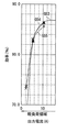
また、図19は、図15〜図18のそれぞれの場合におけるスイッチング電源装置の効率を、出力電流対効率特性図としてまとめたものである。ここで、図中の符号G51〜G53で示した曲線はそれぞれ、コンデンサC1,C2の両方を接続している場合(図15〜図18の(A)図に対応する)、コンデンサC2のみを切断している場合(図15〜図18の(B)図に対応する)、およびコンデンサC1,C2の両方を切断している場合(図15〜図18の(C)図に対応する)を表している。また、各図の縦軸は効率(%)を、横軸は出力電流Iout(A)を表している。また、図中、一例としてそれぞれ、定格負荷領域を出力電流Ioutが50A以上の領域と、中間負荷領域を出力電流Ioutが30〜50Aの領域と、軽負荷領域を出力電流Ioutが0〜30Aの領域として表している。 FIG. 19 summarizes the efficiency of the switching power supply in each case of FIGS. 15 to 18 as an output current versus efficiency characteristic diagram. Here, the curves indicated by reference numerals G51 to G53 in the figure respectively cut only the capacitor C2 when both of the capacitors C1 and C2 are connected (corresponding to FIGS. 15A to 18A). (Corresponding to FIG. 15B to FIG. 18B) and when both capacitors C1 and C2 are disconnected (corresponding to FIG. 15C to FIG. 18C). ing. In each figure, the vertical axis represents efficiency (%) and the horizontal axis represents output current Iout (A). Also, in the figure, as an example, the rated load region is the region where the output current Iout is 50 A or more, the intermediate load region is the region where the output current Iout is 30 to 50 A, and the light load region is the output current Iout is 0 to 30 A. It is expressed as a region.
このように、軽負荷領域および中間負荷領域では、曲線G51と比べて、曲線G52,G53の場合のほうが効率が向上しており、軽負荷領域では曲線G53の場合が特に効率が向上していることが分かる。よって、負荷が小さくなるに応じて、すなわち出力電流Ioutが小さくなるに応じてコンデンサを切断するように制御することで、スイッチング素子の短絡損失Plossを抑制し、軽負荷領域から定格負荷領域に至る広範な領域において、高効率化を図ることができる。 Thus, in the light load region and the intermediate load region, the efficiency is improved in the case of the curves G52 and G53 compared to the curve G51, and in the light load region, the efficiency is particularly improved in the case of the curve G53. I understand that. Therefore, by controlling so that the capacitor is disconnected as the load decreases, that is, as the output current Iout decreases, the short-circuit loss Ploss of the switching element is suppressed and the light load region reaches the rated load region. High efficiency can be achieved in a wide area.
以上のように、本実施の形態では、スイッチング素子S1A〜S4AにコンデンサC1〜C4を並列接続することで、これらコンデンサC1〜C4とインダクタ2とにより適切な共振回路を構成し、この共振回路の共振特性によってスイッチング位相差をなすスイッチング素子の短絡損失を抑制すると共に、容量素子制御回路62によって、固定側スイッチング素子のコンデンサC1,C2の容量値を、負荷8の大きさ(出力電流Ioutの大きさ)に応じて変化させるようにしたので、負荷8の大きさに応じて共振回路の特性を適切なものとすることができ、定格負荷領域における高効率を維持しつつ、軽負荷領域および中間負荷領域においても高効率化を図ることが可能となる。
As described above, in the present embodiment, by connecting the capacitors C1 to C4 in parallel to the switching elements S1A to S4A, an appropriate resonance circuit is configured by the capacitors C1 to C4 and the
以上、実施の形態を挙げて本発明を説明したが、本発明はこの実施の形態に限定されるものではなく、種々の変形が可能である。 While the present invention has been described with reference to the embodiment, the present invention is not limited to this embodiment, and various modifications can be made.
例えば、上記実施の形態では、容量素子としてのコンデンサC1〜C4が、スイッチング素子S1A〜S4Aの全てに並列接続されている場合について説明してきたが、この容量素子としてのコンデンサは、スイッチング素子S1A〜S4Aのうちの少なくとも1つと並列接続されていればよい。このように構成した場合でも、上記実施の形態の場合と同様の効果を得ることができる。 For example, in the above-described embodiment, the case where the capacitors C1 to C4 as the capacitive elements are connected in parallel to all the switching elements S1A to S4A has been described, but the capacitors as the capacitive elements are the switching elements S1A to S1A to S1A to S4A. What is necessary is just to be connected in parallel with at least one of S4A. Even when configured in this manner, the same effects as those of the above-described embodiment can be obtained.
また、上記実施の形態では、軽負荷領域および中間負荷領域において、固定側スイッチング素子のコンデンサC1,C2の接続を切断するように制御する場合について説明してきたが、図20(軽負荷領域)および図21(中間負荷領域)に示したように、これに加えてシフト側スイッチング素子のコンデンサC3,C4の接続を切断するように制御してもよく、また、シフト側スイッチング素子のコンデンサC3,C4のみの接続を切断するように制御してもよい。つまり、容量素子制御回路62は、並列接続されているコンデンサC1〜C4のうちの少なくとも1つのコンデンサの容量値を変化させるように制御すればよい。例えば、図22は、図20および図21の構成のスイッチング電源装置を、前述の具体例に対応させた場合における出力電流対効率特性を表すものである。ここで、図中の符号G53〜G55で示した曲線はそれぞれ、固定側スイッチング素子のコンデンサC1,C2の両方を切断し、かつシフト側スイッチング素子のコンデンサC3,C4の両方を接続している場合(図19の曲線G53)、シフト側スイッチング素子のコンデンサC3のみを接続している場合、およびコンデンサC1〜C4のいずれも切断している場合を表している。このように、軽負荷領域のうちでも特に出力電流Ioutが5A以下の領域において、曲線G53と比べて、曲線G54,G55の場合のほうが効率が向上しており、曲線G55の場合が特に効率が向上していることが分かる。よって、固定側スイッチング素子のコンデンサC1,C2に加えて、シフト側スイッチング素子のコンデンサC3,C4の接続を制御するように構成することで、より軽負荷領域における効率を向上させることが可能となる。なお、固定側スイッチング素子のコンデンサC1,C2の容量値を変化させた場合と、シフト側スイッチング素子のコンデンサC3,C4の容量値を変化させた場合とで効率を向上させる度合いが異なるのは、前述のようにそれぞれの場合における共振回路のインダクタンス値が異なるためである。つまり、シフト側スイッチング素子のコンデンサC3,C4により共振回路を構成した場合よりも、固定側スイッチング素子のコンデンサC1,C2により共振回路を構成した場合のほうがインダクタンス値が小さいので、固定側スイッチング素子のコンデンサC1,C2の容量値を変化させたほうが、より効率を向上させる効果が大きい。
In the above-described embodiment, the case where control is performed so as to disconnect the capacitors C1 and C2 of the fixed-side switching element in the light load region and the intermediate load region has been described. As shown in FIG. 21 (intermediate load region), in addition to this, control may be performed so as to disconnect the capacitors C3 and C4 of the shift side switching element, and the capacitors C3 and C4 of the shift side switching element. It may be controlled to disconnect only the connection. That is, the capacitive
また、上記実施の形態では、容量素子としてのコンデンサC1〜C4が、スイッチング素子S1A〜S4Aそれぞれに対して1つずつ並列接続されている場合について説明してきたが、図23に示したように、例えば、スイッチング素子S5Aに並列接続される容量素子としてのコンデンサを、互いに並列接続された複数のコンデンサC51〜C5nから構成するようにしてもよい。ここで、コンデンサ切断素子S5B1〜S5Bnおよびコンデンサ切断信号L5B1〜L5Bnはそれぞれ、これら複数のコンデンサC51〜C5nに対応させたものである。このように容量素子としてのコンデンサを構成し、これら複数のコンデンサC51〜C5nの接続を選択的にオン・オフ制御するようにした場合、上記実施の形態における効果に加え、容量素子としてのコンデンサの容量値を多段階に変化させることで、より確実に効率を向上させることが可能となる。 Further, in the above embodiment, the case where the capacitors C1 to C4 as the capacitive elements are connected in parallel to the switching elements S1A to S4A one by one has been described, but as shown in FIG. For example, a capacitor as a capacitive element connected in parallel to the switching element S5A may be composed of a plurality of capacitors C51 to C5n connected in parallel to each other. Here, the capacitor cutting elements S5B1 to S5Bn and the capacitor cutting signals L5B1 to L5Bn correspond to the plurality of capacitors C51 to C5n, respectively. When the capacitor as the capacitive element is configured as described above and the connection of the plurality of capacitors C51 to C5n is selectively controlled to be turned on / off, in addition to the effects in the embodiment, the capacitor as the capacitive element By changing the capacitance value in multiple stages, the efficiency can be improved more reliably.
さらに、上記実施の形態では、スイッチング電源装置の回路構成を具体的に挙げて説明したが、回路構成はこれに限定されるものではなく、例えば、トランス3をセンタタップ型以外の他の回路構成としてもよく、また例えば、整流回路4をカソードコモン接続以外の他の回路構成としてもよい。
Furthermore, in the above embodiment, the circuit configuration of the switching power supply device has been specifically described. However, the circuit configuration is not limited to this, and for example, the
1…スイッチング回路、2…インダクタ、3…トランス、31…1次側巻線、32,33…2次側巻線、4…整流回路、5…平滑回路、61…電流検出回路、62…容量素子制御回路、7…スイッチング駆動回路、8…負荷、S1A〜S4A…スイッチング素子、S1B〜S4B…コンデンサ切断素子、C1〜C4…コンデンサ、L1A〜L4A…スイッチング駆動信号、L1B〜L4B…コンデンサ切断信号、L1H…1次側高圧ライン、L1L…1次低圧ライン、LO…出力ライン、LG…接地ライン、P1〜P10…接続点、T1,T2…入力端子、T3,T4…出力端子、Iout…出力電流、Vin…直流入力電圧、Vout…直流出力電圧。
DESCRIPTION OF
Claims (6)
前記第1および第2のスイッチング素子のうちの少なくとも一方と並列に外付け接続された第1の容量素子と、
1次側入力および2次側出力を有すると共にこの1次側入力が前記第1の接続点と前記第2の接続点との間に接続され、前記交流電圧を変圧するトランスと、
前記第1の接続点から前記トランスの1次側入力を経由して前記第2の接続点に至る経路内に挿入され、前記第1の容量素子と共に、ZVS(Zero Volt Switching)動作を行うための共振回路を構成するインダクタと、
前記トランスの2次側出力と接続され、前記トランスによって変圧された交流電圧に基づいて直流出力電圧を生成する出力回路と、
前記第1および第4のスイッチング素子、または前記第2および第3のスイッチング素子に対してそれぞれ、固定側スイッチング素子としての前記第1および第2のスイッチング素子を基準として、シフト側スイッチング素子としての前記第4および第3のスイッチング素子との間にスイッチング位相差をなすように、これらのスイッチング素子を位相シフト制御により駆動するスイッチング駆動回路と、
前記出力回路の負荷の大きさに応じて、前記第1の容量素子のうちの少なくとも1つの容量値が変化するように制御する容量素子制御回路と
を備えたことを特徴とするスイッチング電源装置。 Including first to fourth switching elements, one ends of the first and second switching elements are connected to each other to form a first connection point, and one ends of the third and fourth switching elements are A DC input voltage applied between the other ends of the first and third switching elements and the other ends of the second and fourth switching elements is connected to each other to form a second connection point. A switching circuit that converts AC to AC voltage;
A first capacitive element externally connected in parallel with at least one of the first and second switching elements ;
A transformer having a primary side input and a secondary side output, the primary side input being connected between the first connection point and the second connection point, and transforming the AC voltage;
In order to perform ZVS (Zero Volt Switching) operation together with the first capacitive element, inserted into a path from the first connection point to the second connection point via the primary side input of the transformer. An inductor constituting the resonance circuit of
An output circuit connected to the secondary side output of the transformer and generating a DC output voltage based on the AC voltage transformed by the transformer;
With respect to the first and fourth switching elements, or the second and third switching elements, the first and second switching elements as fixed-side switching elements are used as references, and as shift-side switching elements, respectively. a switching drive circuit for driving the phase shift control so as to have a switching phase difference, these switching elements between said fourth and third switching elements,
A switching power supply device comprising: a capacitor element control circuit that controls the capacitance value of at least one of the first capacitor elements to change in accordance with the load of the output circuit.
前記容量素子制御回路は、前記第1および第2の容量素子のうち、前記第1の容量素子における容量値のみが変化するように制御する
ことを特徴とする請求項1に記載のスイッチング電源装置。 A second capacitive element externally connected in parallel with at least one of the third and fourth switching elements;
2. The switching power supply device according to claim 1, wherein the capacitive element control circuit performs control so that only a capacitance value of the first capacitive element among the first and second capacitive elements changes. .
ことを特徴とする請求項1または請求項2に記載のスイッチング電源装置。 The capacitive element control circuit, according to the load of the output circuit is smaller, at least one capacitance value and controls so as to become smaller according to claim 1, wherein one of said first capacitive element Item 3. The switching power supply device according to Item 2 .
前記容量素子制御回路は、前記第1の容量素子とこの第1の容量素子に並列接続されたスイッチング素子との間の接続をオン・オフ制御することによって、前記第1の容量素子の容量値が変化するように制御する
ことを特徴とする請求項1ないし請求項3のいずれか1項に記載のスイッチング電源装置。 Each of the first to fourth switching elements has a parasitic capacitance,
The capacitor element control circuit, by controlling on and off the connection between the first capacitor and the first capacitor in parallel-connected switching elements, the capacitance value of the first capacitor The switching power supply according to any one of claims 1 to 3, wherein the switching power supply is controlled to change.
前記容量素子制御回路は、これら複数のコンデンサを用いて前記第1の容量素子の容量値が変化するように制御する
ことを特徴とする請求項1ないし請求項3のいずれか1項に記載のスイッチング電源装置。 At least one of the first capacitive elements is composed of a plurality of capacitors connected in parallel to each other;
The said capacitive element control circuit controls so that the capacitance value of a said 1st capacitive element may change using these several capacitor | condensers. The Claim 1 thru | or 3 characterized by the above-mentioned. Switching power supply.
ことを特徴とする請求項5に記載のスイッチング電源装置。 The said capacitive element control circuit controls so that the capacitance value of a said 1st capacitive element may change by selectively turning on / off each connection of these several capacitor | condenser. 5. The switching power supply device according to 5.
Priority Applications (1)
| Application Number | Priority Date | Filing Date | Title |
|---|---|---|---|
| JP2004347863A JP4635584B2 (en) | 2004-11-30 | 2004-11-30 | Switching power supply |
Applications Claiming Priority (1)
| Application Number | Priority Date | Filing Date | Title |
|---|---|---|---|
| JP2004347863A JP4635584B2 (en) | 2004-11-30 | 2004-11-30 | Switching power supply |
Publications (2)
| Publication Number | Publication Date |
|---|---|
| JP2006158137A JP2006158137A (en) | 2006-06-15 |
| JP4635584B2 true JP4635584B2 (en) | 2011-02-23 |
Family
ID=36635737
Family Applications (1)
| Application Number | Title | Priority Date | Filing Date |
|---|---|---|---|
| JP2004347863A Expired - Fee Related JP4635584B2 (en) | 2004-11-30 | 2004-11-30 | Switching power supply |
Country Status (1)
| Country | Link |
|---|---|
| JP (1) | JP4635584B2 (en) |
Families Citing this family (6)
| Publication number | Priority date | Publication date | Assignee | Title |
|---|---|---|---|---|
| JP2009100554A (en) * | 2007-10-17 | 2009-05-07 | Sharp Corp | Partial voltage resonance type switching power supply circuit and air conditioner equipped with same |
| JP5642621B2 (en) * | 2011-05-13 | 2014-12-17 | コーセル株式会社 | Switching power supply |
| JP5342623B2 (en) * | 2011-09-15 | 2013-11-13 | 三菱電機株式会社 | Switching power supply |
| JP5906418B2 (en) * | 2012-06-15 | 2016-04-20 | パナソニックIpマネジメント株式会社 | Power converter |
| CN104426408B (en) | 2013-09-05 | 2017-06-30 | 台达电子企业管理(上海)有限公司 | Translation circuit and be applied to translation circuit conversion electric power changing method |
| JP2015181329A (en) | 2014-03-04 | 2015-10-15 | パナソニックIpマネジメント株式会社 | Electric power conversion system |
Citations (1)
| Publication number | Priority date | Publication date | Assignee | Title |
|---|---|---|---|---|
| WO2001071896A1 (en) * | 2000-03-23 | 2001-09-27 | Tdk Corporation | Switching power supply |
Family Cites Families (1)
| Publication number | Priority date | Publication date | Assignee | Title |
|---|---|---|---|---|
| JPH04125062A (en) * | 1990-09-12 | 1992-04-24 | Toyota Autom Loom Works Ltd | Series resonance type dc-dc converter |
-
2004
- 2004-11-30 JP JP2004347863A patent/JP4635584B2/en not_active Expired - Fee Related
Patent Citations (1)
| Publication number | Priority date | Publication date | Assignee | Title |
|---|---|---|---|---|
| WO2001071896A1 (en) * | 2000-03-23 | 2001-09-27 | Tdk Corporation | Switching power supply |
Also Published As
| Publication number | Publication date |
|---|---|
| JP2006158137A (en) | 2006-06-15 |
Similar Documents
| Publication | Publication Date | Title |
|---|---|---|
| JP5590124B2 (en) | DC-DC converter | |
| US8107263B2 (en) | Series resonant converter | |
| US8542501B2 (en) | Switching power-supply apparatus | |
| US8441812B2 (en) | Series resonant converter having a circuit configuration that prevents leading current | |
| US7242595B2 (en) | Switching power supply circuit | |
| EP1609235B1 (en) | Phase-shifted resonant converter having reduced output ripple | |
| US20080037290A1 (en) | Ac-dc converter and method for driving for ac-dc converter | |
| JP2014011940A (en) | Current resonant dc-dc converter | |
| US11296607B2 (en) | DC-DC converter | |
| US10505462B2 (en) | Power converter | |
| US10020749B2 (en) | Power conversion unit | |
| JP2015181329A (en) | Electric power conversion system | |
| US20230223856A1 (en) | Power conversion apparatus having multiple llc converters and capable of achieving desired output voltage even in changes in load current | |
| US20150194897A1 (en) | Power supply apparatus | |
| JP6388154B2 (en) | Resonant type DC-DC converter | |
| JP2009060747A (en) | Dc-dc converter | |
| US11356029B2 (en) | Rectifying circuit and switched-mode power supply incorporating rectifying circuit | |
| JP4635584B2 (en) | Switching power supply | |
| JP5105819B2 (en) | DC-DC converter | |
| JP2015154525A (en) | bidirectional flyback converter | |
| JP6245372B2 (en) | Power conversion apparatus and wireless power transmission system | |
| JP2014075944A (en) | Bidirectional converter | |
| JP2003259644A (en) | Switching converter circuit | |
| JP7386737B2 (en) | Rectifier circuit and switching power supply using the same | |
| KR101435469B1 (en) | Zero voltage switching dc-dc converter |
Legal Events
| Date | Code | Title | Description |
|---|---|---|---|
| A621 | Written request for application examination |
Free format text: JAPANESE INTERMEDIATE CODE: A621 Effective date: 20070801 |
|
| A131 | Notification of reasons for refusal |
Free format text: JAPANESE INTERMEDIATE CODE: A131 Effective date: 20100623 |
|
| A521 | Written amendment |
Free format text: JAPANESE INTERMEDIATE CODE: A523 Effective date: 20100819 |
|
| TRDD | Decision of grant or rejection written | ||
| A01 | Written decision to grant a patent or to grant a registration (utility model) |
Free format text: JAPANESE INTERMEDIATE CODE: A01 Effective date: 20101026 |
|
| A01 | Written decision to grant a patent or to grant a registration (utility model) |
Free format text: JAPANESE INTERMEDIATE CODE: A01 |
|
| A61 | First payment of annual fees (during grant procedure) |
Free format text: JAPANESE INTERMEDIATE CODE: A61 Effective date: 20101108 |
|
| FPAY | Renewal fee payment (event date is renewal date of database) |
Free format text: PAYMENT UNTIL: 20131203 Year of fee payment: 3 |
|
| R150 | Certificate of patent or registration of utility model |
Free format text: JAPANESE INTERMEDIATE CODE: R150 Ref document number: 4635584 Country of ref document: JP Free format text: JAPANESE INTERMEDIATE CODE: R150 |
|
| LAPS | Cancellation because of no payment of annual fees |