JP4627140B2 - Display device - Google Patents
Display device Download PDFInfo
- Publication number
- JP4627140B2 JP4627140B2 JP2003357882A JP2003357882A JP4627140B2 JP 4627140 B2 JP4627140 B2 JP 4627140B2 JP 2003357882 A JP2003357882 A JP 2003357882A JP 2003357882 A JP2003357882 A JP 2003357882A JP 4627140 B2 JP4627140 B2 JP 4627140B2
- Authority
- JP
- Japan
- Prior art keywords
- flexible substrate
- display device
- reinforcing member
- reinforcing
- terminal group
- Prior art date
- Legal status (The legal status is an assumption and is not a legal conclusion. Google has not performed a legal analysis and makes no representation as to the accuracy of the status listed.)
- Expired - Lifetime
Links
- 239000000758 substrate Substances 0.000 claims description 81
- 230000003014 reinforcing effect Effects 0.000 claims description 56
- 239000012779 reinforcing material Substances 0.000 claims description 20
- 239000000463 material Substances 0.000 description 15
- 239000002274 desiccant Substances 0.000 description 9
- 239000003795 chemical substances by application Substances 0.000 description 7
- 238000007789 sealing Methods 0.000 description 7
- 239000000565 sealant Substances 0.000 description 6
- 238000010586 diagram Methods 0.000 description 4
- 239000010408 film Substances 0.000 description 4
- 239000004973 liquid crystal related substance Substances 0.000 description 4
- 238000005401 electroluminescence Methods 0.000 description 3
- 239000004065 semiconductor Substances 0.000 description 3
- 238000005452 bending Methods 0.000 description 2
- 230000015572 biosynthetic process Effects 0.000 description 2
- 239000004020 conductor Substances 0.000 description 2
- 239000011521 glass Substances 0.000 description 2
- 239000012212 insulator Substances 0.000 description 2
- 239000011159 matrix material Substances 0.000 description 2
- 239000010409 thin film Substances 0.000 description 2
- 239000004642 Polyimide Substances 0.000 description 1
- 239000000470 constituent Substances 0.000 description 1
- 230000000694 effects Effects 0.000 description 1
- 239000003822 epoxy resin Substances 0.000 description 1
- 238000004519 manufacturing process Methods 0.000 description 1
- 230000003647 oxidation Effects 0.000 description 1
- 238000007254 oxidation reaction Methods 0.000 description 1
- 230000002093 peripheral effect Effects 0.000 description 1
- 239000004417 polycarbonate Substances 0.000 description 1
- 229920000515 polycarbonate Polymers 0.000 description 1
- 229920000647 polyepoxide Polymers 0.000 description 1
- -1 polyethylene terephthalate Polymers 0.000 description 1
- 229920000139 polyethylene terephthalate Polymers 0.000 description 1
- 239000005020 polyethylene terephthalate Substances 0.000 description 1
- 229920001721 polyimide Polymers 0.000 description 1
- 230000002265 prevention Effects 0.000 description 1
- 229920005989 resin Polymers 0.000 description 1
- 239000011347 resin Substances 0.000 description 1
Images


Classifications
-
- G—PHYSICS
- G09—EDUCATION; CRYPTOGRAPHY; DISPLAY; ADVERTISING; SEALS
- G09G—ARRANGEMENTS OR CIRCUITS FOR CONTROL OF INDICATING DEVICES USING STATIC MEANS TO PRESENT VARIABLE INFORMATION
- G09G3/00—Control arrangements or circuits, of interest only in connection with visual indicators other than cathode-ray tubes
- G09G3/20—Control arrangements or circuits, of interest only in connection with visual indicators other than cathode-ray tubes for presentation of an assembly of a number of characters, e.g. a page, by composing the assembly by combination of individual elements arranged in a matrix no fixed position being assigned to or needed to be assigned to the individual characters or partial characters
- G09G3/22—Control arrangements or circuits, of interest only in connection with visual indicators other than cathode-ray tubes for presentation of an assembly of a number of characters, e.g. a page, by composing the assembly by combination of individual elements arranged in a matrix no fixed position being assigned to or needed to be assigned to the individual characters or partial characters using controlled light sources
- G09G3/30—Control arrangements or circuits, of interest only in connection with visual indicators other than cathode-ray tubes for presentation of an assembly of a number of characters, e.g. a page, by composing the assembly by combination of individual elements arranged in a matrix no fixed position being assigned to or needed to be assigned to the individual characters or partial characters using controlled light sources using electroluminescent panels
- G09G3/32—Control arrangements or circuits, of interest only in connection with visual indicators other than cathode-ray tubes for presentation of an assembly of a number of characters, e.g. a page, by composing the assembly by combination of individual elements arranged in a matrix no fixed position being assigned to or needed to be assigned to the individual characters or partial characters using controlled light sources using electroluminescent panels semiconductive, e.g. using light-emitting diodes [LED]
- G09G3/3208—Control arrangements or circuits, of interest only in connection with visual indicators other than cathode-ray tubes for presentation of an assembly of a number of characters, e.g. a page, by composing the assembly by combination of individual elements arranged in a matrix no fixed position being assigned to or needed to be assigned to the individual characters or partial characters using controlled light sources using electroluminescent panels semiconductive, e.g. using light-emitting diodes [LED] organic, e.g. using organic light-emitting diodes [OLED]
- G09G3/3225—Control arrangements or circuits, of interest only in connection with visual indicators other than cathode-ray tubes for presentation of an assembly of a number of characters, e.g. a page, by composing the assembly by combination of individual elements arranged in a matrix no fixed position being assigned to or needed to be assigned to the individual characters or partial characters using controlled light sources using electroluminescent panels semiconductive, e.g. using light-emitting diodes [LED] organic, e.g. using organic light-emitting diodes [OLED] using an active matrix
- G09G3/3233—Control arrangements or circuits, of interest only in connection with visual indicators other than cathode-ray tubes for presentation of an assembly of a number of characters, e.g. a page, by composing the assembly by combination of individual elements arranged in a matrix no fixed position being assigned to or needed to be assigned to the individual characters or partial characters using controlled light sources using electroluminescent panels semiconductive, e.g. using light-emitting diodes [LED] organic, e.g. using organic light-emitting diodes [OLED] using an active matrix with pixel circuitry controlling the current through the light-emitting element
-
- H—ELECTRICITY
- H10—SEMICONDUCTOR DEVICES; ELECTRIC SOLID-STATE DEVICES NOT OTHERWISE PROVIDED FOR
- H10K—ORGANIC ELECTRIC SOLID-STATE DEVICES
- H10K50/00—Organic light-emitting devices
- H10K50/80—Constructional details
-
- H—ELECTRICITY
- H10—SEMICONDUCTOR DEVICES; ELECTRIC SOLID-STATE DEVICES NOT OTHERWISE PROVIDED FOR
- H10K—ORGANIC ELECTRIC SOLID-STATE DEVICES
- H10K59/00—Integrated devices, or assemblies of multiple devices, comprising at least one organic light-emitting element covered by group H10K50/00
- H10K59/10—OLED displays
- H10K59/12—Active-matrix OLED [AMOLED] displays
- H10K59/1201—Manufacture or treatment
-
- H—ELECTRICITY
- H10—SEMICONDUCTOR DEVICES; ELECTRIC SOLID-STATE DEVICES NOT OTHERWISE PROVIDED FOR
- H10K—ORGANIC ELECTRIC SOLID-STATE DEVICES
- H10K59/00—Integrated devices, or assemblies of multiple devices, comprising at least one organic light-emitting element covered by group H10K50/00
- H10K59/10—OLED displays
- H10K59/12—Active-matrix OLED [AMOLED] displays
- H10K59/131—Interconnections, e.g. wiring lines or terminals
-
- G—PHYSICS
- G09—EDUCATION; CRYPTOGRAPHY; DISPLAY; ADVERTISING; SEALS
- G09G—ARRANGEMENTS OR CIRCUITS FOR CONTROL OF INDICATING DEVICES USING STATIC MEANS TO PRESENT VARIABLE INFORMATION
- G09G2300/00—Aspects of the constitution of display devices
- G09G2300/08—Active matrix structure, i.e. with use of active elements, inclusive of non-linear two terminal elements, in the pixels together with light emitting or modulating elements
- G09G2300/0809—Several active elements per pixel in active matrix panels
- G09G2300/0819—Several active elements per pixel in active matrix panels used for counteracting undesired variations, e.g. feedback or autozeroing
-
- G—PHYSICS
- G09—EDUCATION; CRYPTOGRAPHY; DISPLAY; ADVERTISING; SEALS
- G09G—ARRANGEMENTS OR CIRCUITS FOR CONTROL OF INDICATING DEVICES USING STATIC MEANS TO PRESENT VARIABLE INFORMATION
- G09G2300/00—Aspects of the constitution of display devices
- G09G2300/08—Active matrix structure, i.e. with use of active elements, inclusive of non-linear two terminal elements, in the pixels together with light emitting or modulating elements
- G09G2300/0809—Several active elements per pixel in active matrix panels
- G09G2300/0842—Several active elements per pixel in active matrix panels forming a memory circuit, e.g. a dynamic memory with one capacitor
- G09G2300/0852—Several active elements per pixel in active matrix panels forming a memory circuit, e.g. a dynamic memory with one capacitor being a dynamic memory with more than one capacitor
-
- G—PHYSICS
- G09—EDUCATION; CRYPTOGRAPHY; DISPLAY; ADVERTISING; SEALS
- G09G—ARRANGEMENTS OR CIRCUITS FOR CONTROL OF INDICATING DEVICES USING STATIC MEANS TO PRESENT VARIABLE INFORMATION
- G09G2300/00—Aspects of the constitution of display devices
- G09G2300/08—Active matrix structure, i.e. with use of active elements, inclusive of non-linear two terminal elements, in the pixels together with light emitting or modulating elements
- G09G2300/0809—Several active elements per pixel in active matrix panels
- G09G2300/0842—Several active elements per pixel in active matrix panels forming a memory circuit, e.g. a dynamic memory with one capacitor
- G09G2300/0861—Several active elements per pixel in active matrix panels forming a memory circuit, e.g. a dynamic memory with one capacitor with additional control of the display period without amending the charge stored in a pixel memory, e.g. by means of additional select electrodes
-
- G—PHYSICS
- G09—EDUCATION; CRYPTOGRAPHY; DISPLAY; ADVERTISING; SEALS
- G09G—ARRANGEMENTS OR CIRCUITS FOR CONTROL OF INDICATING DEVICES USING STATIC MEANS TO PRESENT VARIABLE INFORMATION
- G09G2320/00—Control of display operating conditions
- G09G2320/04—Maintaining the quality of display appearance
- G09G2320/043—Preventing or counteracting the effects of ageing
-
- G—PHYSICS
- G09—EDUCATION; CRYPTOGRAPHY; DISPLAY; ADVERTISING; SEALS
- G09G—ARRANGEMENTS OR CIRCUITS FOR CONTROL OF INDICATING DEVICES USING STATIC MEANS TO PRESENT VARIABLE INFORMATION
- G09G3/00—Control arrangements or circuits, of interest only in connection with visual indicators other than cathode-ray tubes
- G09G3/20—Control arrangements or circuits, of interest only in connection with visual indicators other than cathode-ray tubes for presentation of an assembly of a number of characters, e.g. a page, by composing the assembly by combination of individual elements arranged in a matrix no fixed position being assigned to or needed to be assigned to the individual characters or partial characters
- G09G3/22—Control arrangements or circuits, of interest only in connection with visual indicators other than cathode-ray tubes for presentation of an assembly of a number of characters, e.g. a page, by composing the assembly by combination of individual elements arranged in a matrix no fixed position being assigned to or needed to be assigned to the individual characters or partial characters using controlled light sources
- G09G3/30—Control arrangements or circuits, of interest only in connection with visual indicators other than cathode-ray tubes for presentation of an assembly of a number of characters, e.g. a page, by composing the assembly by combination of individual elements arranged in a matrix no fixed position being assigned to or needed to be assigned to the individual characters or partial characters using controlled light sources using electroluminescent panels
- G09G3/32—Control arrangements or circuits, of interest only in connection with visual indicators other than cathode-ray tubes for presentation of an assembly of a number of characters, e.g. a page, by composing the assembly by combination of individual elements arranged in a matrix no fixed position being assigned to or needed to be assigned to the individual characters or partial characters using controlled light sources using electroluminescent panels semiconductive, e.g. using light-emitting diodes [LED]
- G09G3/3208—Control arrangements or circuits, of interest only in connection with visual indicators other than cathode-ray tubes for presentation of an assembly of a number of characters, e.g. a page, by composing the assembly by combination of individual elements arranged in a matrix no fixed position being assigned to or needed to be assigned to the individual characters or partial characters using controlled light sources using electroluminescent panels semiconductive, e.g. using light-emitting diodes [LED] organic, e.g. using organic light-emitting diodes [OLED]
-
- H—ELECTRICITY
- H10—SEMICONDUCTOR DEVICES; ELECTRIC SOLID-STATE DEVICES NOT OTHERWISE PROVIDED FOR
- H10K—ORGANIC ELECTRIC SOLID-STATE DEVICES
- H10K2102/00—Constructional details relating to the organic devices covered by this subclass
- H10K2102/301—Details of OLEDs
- H10K2102/311—Flexible OLED
-
- H—ELECTRICITY
- H10—SEMICONDUCTOR DEVICES; ELECTRIC SOLID-STATE DEVICES NOT OTHERWISE PROVIDED FOR
- H10K—ORGANIC ELECTRIC SOLID-STATE DEVICES
- H10K59/00—Integrated devices, or assemblies of multiple devices, comprising at least one organic light-emitting element covered by group H10K50/00
- H10K59/10—OLED displays
- H10K59/12—Active-matrix OLED [AMOLED] displays
-
- H—ELECTRICITY
- H10—SEMICONDUCTOR DEVICES; ELECTRIC SOLID-STATE DEVICES NOT OTHERWISE PROVIDED FOR
- H10K—ORGANIC ELECTRIC SOLID-STATE DEVICES
- H10K71/00—Manufacture or treatment specially adapted for the organic devices covered by this subclass
- H10K71/80—Manufacture or treatment specially adapted for the organic devices covered by this subclass using temporary substrates
Landscapes
- Engineering & Computer Science (AREA)
- Physics & Mathematics (AREA)
- Microelectronics & Electronic Packaging (AREA)
- Computer Hardware Design (AREA)
- General Physics & Mathematics (AREA)
- Theoretical Computer Science (AREA)
- Manufacturing & Machinery (AREA)
- Optics & Photonics (AREA)
- Electroluminescent Light Sources (AREA)
- Devices For Indicating Variable Information By Combining Individual Elements (AREA)
Description
本発明は表示装置に係り、それ自体が可撓性を有する表示装置に関する。 The present invention relates to a display device, and more particularly to a display device having flexibility.
たとえば、有機EL表示装置等の表示装置は、その基板の一方の面にそのx方向に延在しy方向に並設されるゲート信号線とy方向に延在しx方向に並設されるドレイン信号線とで囲まれた領域を画素領域とし、この画素領域に、ゲート信号線からの走査信号線によってオンする薄膜トランジスタと、この薄膜トランジスタを介して供給されるドレイン信号線からの映像信号に対応する電流を流す発光層(有機EL層)を少なくとも備えている。 For example, a display device such as an organic EL display device is arranged on one surface of the substrate in the x direction and in parallel with the gate signal line extending in the y direction and in the x direction. A region surrounded by the drain signal line is defined as a pixel region, and a thin film transistor that is turned on by the scanning signal line from the gate signal line and a video signal from the drain signal line supplied through the thin film transistor are supported in the pixel region. At least a light emitting layer (organic EL layer) through which a current to flow is supplied.
そして、該発光層は、酸化、あるいは湿気によってその特性が劣化することから、前記基板とは異なる他の基板であって、発光層を外気と遮蔽するための基板を備えさせ、このように外気と遮蔽された空間内に乾燥剤を配置させているのが通常である。 Since the characteristics of the light emitting layer deteriorate due to oxidation or moisture, the light emitting layer is provided with a substrate that is different from the substrate and shields the light emitting layer from the outside air. Usually, a desiccant is disposed in the shielded space.
また、これら各基板としてはたとえばガラス基板からなるものもあるが、たとえば樹脂からなるものも知られるに至り、有機EL表示装置自体にフレキシブル性(可撓性)を有するようになってきているものがある(特許文献1ないし4参照)。 In addition, some of these substrates are made of, for example, a glass substrate. However, for example, those made of resin are also known, and the organic EL display device itself has become flexible (flexible). (See Patent Documents 1 to 4).
しかしながら、このように構成される表示装置は、外部から信号を供給するための端子(端子群)がフレキシブル基板の上方に形成されているため、その端子群が形成された個所においても撓みやすく構成されている。 However, the display device configured as described above is configured such that terminals (terminal groups) for supplying signals from the outside are formed above the flexible substrate, so that they are easily bent even at the locations where the terminal groups are formed. Has been.
該端子群はフレキシブル配線基板に接続され、このフレキシブル配線基板を介して信号が供給されるようになっているが、上述のように端子群の個所にて撓みやすくなっていることから、該フレキシブル配線基板との接続不良を起こしやすいということが指摘されるに至った。 The terminal group is connected to a flexible wiring board, and signals are supplied through the flexible wiring board. However, since the terminal group is easily bent at the terminal group as described above, It has been pointed out that poor connection with the wiring board is likely to occur.
本発明は、このような事情に基づいてなされたもので、その目的は、基板自体の可撓性を損なうことなく、端子群とこれに接続されるフレキシブル配線基板との接続を充分に確保できる表示装置を提供することにある。 The present invention has been made based on such circumstances, and the object thereof is to sufficiently secure the connection between the terminal group and the flexible wiring board connected thereto without impairing the flexibility of the substrate itself. It is to provide a display device.
本願において開示される発明のうち、代表的なものの概要を簡単に説明すれば、以下のとおりである。
(1)
本発明による表示装置は、たとえば、フレキシブル基板を少なくとも外囲器の一部とするものであって、該フレキシブル基板の一方の側に信号を供給する端子群が形成され、該フレキシブル基板のうち少なくとも前記端子群が形成された部分と反対側の前記フレキシブル基板の面の部分に補強部材が取り付けられていることを特徴とするものである。
Of the inventions disclosed in this application, the outline of typical ones will be briefly described as follows.
(1)
The display device according to the present invention has, for example, a flexible substrate as at least a part of an envelope, and a terminal group that supplies a signal to one side of the flexible substrate is formed. A reinforcing member is attached to a portion of the surface of the flexible substrate opposite to the portion where the terminal group is formed.
(2)
本発明による表示装置は、たとえば、フレキシブル基板を少なくとも外囲器の一部とするものであって、該フレキシブル基板の一方の側に信号を供給する端子群が形成され、該端子群に接続されるフレキシブル配線基板を備え、
該フレキシブル基板のうち少なくとも前記端子群が形成された部分と反対側の面の部分に補強部材が取り付けられていることを特徴とするものである。
(2)
The display device according to the present invention has, for example, a flexible substrate as at least a part of an envelope, and a terminal group that supplies a signal to one side of the flexible substrate is formed and connected to the terminal group. Flexible wiring board
A reinforcing member is attached to at least a portion of the surface of the flexible substrate opposite to the portion where the terminal group is formed.
(3)
本発明による表示装置は、たとえば、(1)、(2)のいずれかの構成を前提とし、フレキシブル配線基板は、その周辺の少なくとも一部に該端子群が形成された材料層に跨って塗付された補強材が形成されていることを特徴とするものである。
(3)
The display device according to the present invention is premised on, for example, the configuration of (1) or (2), and the flexible wiring board is applied across the material layer in which the terminal group is formed on at least a part of the periphery thereof. The attached reinforcing material is formed.
(4)
本発明による表示装置は、たとえば、(1)、(2)のいずれかの構成を前提とし、前記補強部材はその周辺の少なくとも一部にフレキシブル基板に跨って塗付された補強材が形成されていることを特徴とするものである。
(4)
The display device according to the present invention is premised on, for example, the configuration of either (1) or (2), and the reinforcing member is formed with a reinforcing material applied across at least a part of the periphery thereof across the flexible substrate. It is characterized by that.
(5)
本発明による表示装置は、たとえば、フレキシブル基板を少なくとも外囲器の一部とするものであって、該フレキシブル基板の一方の側に信号を供給する端子群が形成され、この端子群であって隣接する端子同士でグループ別されたそれぞれの端子群ごとに接続される複数のフレキシブル配線基板を備え、
前記フレキシブル基板のうち前記端子群が形成された部分と反対側の面の部分に前記グループ別されたそれぞれの端子群毎に補強部材が取り付けられていることを特徴とするものである。
(5)
The display device according to the present invention has, for example, a flexible substrate as at least a part of an envelope, and a terminal group for supplying signals to one side of the flexible substrate is formed. A plurality of flexible wiring boards connected to each terminal group grouped by adjacent terminals,
A reinforcing member is attached to each of the grouped terminal groups on a portion of the surface of the flexible substrate opposite to the portion where the terminal groups are formed.
(6)
本発明による表示装置は、たとえば、(5)の構成を前提とし、各フレキシブル配線基板は、異方性導電膜を介して端子群と接続されるとともに、その周辺の少なくとも一部に該端子群が形成された材料層に跨って塗付された補強材が形成されていることを特徴とするものである。
(6)
The display device according to the present invention is premised on, for example, the configuration of (5), and each flexible wiring board is connected to a terminal group via an anisotropic conductive film, and at least a part of the periphery thereof is connected to the terminal group. A reinforcing material applied across the material layer on which is formed is formed.
(7)
本発明による表示装置は、たとえば、(5)の構成を前提とし、前記補強部材はその周辺の少なくとも一部にフレキシブル基板に跨って塗付された補強材が形成されていることを特徴とするものである。
(7)
The display device according to the present invention is, for example, on the premise of the configuration of (5), and the reinforcing member is formed with a reinforcing material applied over at least a part of the periphery thereof across the flexible substrate. Is.
(8)
本発明による表示装置は、たとえば、(1)、(2)、(5)のいずれかの構成を前提とし、フレキシブル基板と補強部材のそれぞれに第1のマークおよび第2のマークが形成され、補強部材はその第2のマークが第1のマークに重畳してフレキシブル基板に被着されていることを特徴とするものである。
(8)
The display device according to the present invention is based on, for example, any one of the constitutions (1), (2), and (5), and the first mark and the second mark are formed on each of the flexible substrate and the reinforcing member. The reinforcing member is characterized in that the second mark is attached to the flexible substrate so as to overlap the first mark.
(9)
本発明による表示装置は、たとえば、(1)、(2)、(5)のいずれかの構成を前提とし、補強部材は板状のパターンで形成されていることを特徴とするものである。
(9)
The display device according to the present invention is characterized in that, for example, the structure of any one of (1), (2), and (5) is assumed, and the reinforcing member is formed in a plate-like pattern.
(10)
本発明による表示装置は、たとえば、(1)、(2)、(5)のいずれかの構成を前提とし、補強部材は環状のパターンで形成されていることを特徴とするものである。
(10)
The display device according to the present invention is characterized in that, for example, the structure of any one of (1), (2), and (5) is assumed, and the reinforcing member is formed in an annular pattern.
なお、本発明は以上の構成に限定されず、本発明の技術思想を逸脱しない範囲で種々の変更が可能である。 In addition, this invention is not limited to the above structure, A various change is possible in the range which does not deviate from the technical idea of this invention.
このように構成された表示装置は、その基板自体の可撓性を損なうことなく、その端子とこれに接続されるプリント配線基板との接続を確保し、前記基板が撓っても結線不良の発生を回避することができるようになる。 The display device configured in this way ensures the connection between the terminal and the printed wiring board connected thereto without damaging the flexibility of the board itself, and even if the board is bent, the connection is poor. Occurrence can be avoided.
以下、本発明による表示装置の実施例を図面を用いて説明する。
図7(a)はたとえば有機EL表示装置の一画素とその近傍の個所を示す平面図である。有機EL表示装置の各画素はたとえば透明な基板の表面にマトリックス状に形成され、そのうちの一つを図7(a)に示している。これら、各画素は、所定のパターンに形成された導電層、半導体層、絶縁層等が適宜積層されることによって微細な電子回路が組み込まれている。
Embodiments of a display device according to the present invention will be described below with reference to the drawings.
FIG. 7A is a plan view showing, for example, one pixel of an organic EL display device and a portion in the vicinity thereof. Each pixel of the organic EL display device is formed in a matrix on the surface of a transparent substrate, for example, and one of them is shown in FIG. Each of these pixels incorporates a fine electronic circuit by appropriately stacking a conductive layer, a semiconductor layer, an insulating layer, and the like formed in a predetermined pattern.
すなわち、該一画素は、その図中上側において当該画素を選択駆動するゲート信号線GLによって画され、左側において当該画素に映像信号を供給するドレイン信号線DLによって画され、右側において当該画素に電流を供給する電流供給線PLによって画され、下側において当該画素と隣接する他の画素を選択駆動するゲート信号線GLによって画されている。 That is, the one pixel is defined by a gate signal line GL that selectively drives the pixel on the upper side in the drawing, is defined by a drain signal line DL that supplies a video signal to the pixel on the left side, and a current is supplied to the pixel on the right side. Is defined by a current supply line PL that supplies the pixel, and is defined by a gate signal line GL that selectively drives other pixels adjacent to the pixel on the lower side.
この一画素の領域は図中上側と下側とに区分され、下側の領域には有機EL層からなる発光層が形成され、上側の領域には前記映像信号対応した電流を形成するための回路が形成されている。 This one pixel region is divided into an upper side and a lower side in the figure, a light emitting layer composed of an organic EL layer is formed in the lower region, and a current corresponding to the video signal is formed in the upper region. A circuit is formed.
発光層が形成された前記領域には、基板側からたとえば透光性の導電層からなる一方の電極(図中ITOで示す)、発光層、他方の電極が順次積層されている。前記発光層は前記一方の電極の上層に形成されたバンク層の開口部(図中BMP,OPN)に埋設されて形成され、この部分が実質的に発光部として構成される。また、前記他方の電極は前記バンク層の上面をも被って各画素に共通に形成されている。 In the region where the light emitting layer is formed, one electrode (indicated by ITO in the figure) made of a light-transmitting conductive layer, the light emitting layer, and the other electrode are sequentially laminated from the substrate side. The light emitting layer is formed by being embedded in an opening (BMP, OPN in the figure) of the bank layer formed on the upper layer of the one electrode, and this portion is substantially configured as a light emitting portion. The other electrode is also formed in common for each pixel covering the upper surface of the bank layer.
前記一方の電極を陽極、他方の電極を陰極として、その間の発光層に電流が流れることによって、該発光層は電流に応じた強度で発光がなされるようになっている。なお、前記バンク層は当該画素からの発光を隣接する画素内に伝達されるのを回避するため、あるいは、製造の工程において当初流動性をもつ発光層を所定の輪郭を有するように形成するために設けられている。 With the one electrode serving as an anode and the other electrode serving as a cathode, a current flows through the light emitting layer therebetween, whereby the light emitting layer emits light with an intensity corresponding to the current. The bank layer is for avoiding that light emitted from the pixel is transmitted to adjacent pixels, or for forming a light-emitting layer having initial fluidity in a manufacturing process so as to have a predetermined contour. Is provided.
前記回路に形成された前記領域には、スイッチング素子SW1、SW2、SW3、スイッチング素子SW2をオン・オフするコントロール信号線CL1、スイッチング素子SW3をオン・オフするコントロール信号線CL2、ドライブ・トランジスタDT、容量素子C1−CSi、CSi−C2が形成されている。 The region formed in the circuit includes switching elements SW1, SW2, SW3, a control signal line CL1 for turning on / off the switching element SW2, a control signal line CL2 for turning on / off the switching element SW3, a drive transistor DT, Capacitance elements C1-CSi and CSi-C2 are formed.
この回路は、ゲート信号線GLからの走査信号によって、ドレイン信号線DLから映像信号を取り込み、この映像信号の強弱(電圧)に応じて、電流供給線PLからの電流を前記発光層が形成された領域の一方の電極に供給するようになっている。 This circuit captures a video signal from the drain signal line DL by a scanning signal from the gate signal line GL, and the light emitting layer forms the current from the current supply line PL according to the strength (voltage) of this video signal. This is supplied to one electrode in the region.
ここで、前記スイッチング素子SW2、SW3、および容量素子Csi−C2は、ドライブ・トランジスタDTの閾値電圧が各画素毎にばらつきがある場合において、そのばらつき補正をするために設けられている。 Here, the switching elements SW2 and SW3 and the capacitive element Csi-C2 are provided to correct the variation when the threshold voltage of the drive transistor DT varies for each pixel.
《等価回路》
図7(b)は前記一画素における等価回路を示し、図7(a)における幾何学的配置にほぼ対応させて描いている。
<< Equivalent circuit >>
FIG. 7B shows an equivalent circuit in the one pixel, which is drawn so as to substantially correspond to the geometric arrangement in FIG.
ゲート信号線GLからの走査信号によって、スイッチング素子SW1がオンし、ドレイン信号線DLからの映像信号が該スイッチング素子SW1を介して容量素子C1−CSiの一方の電極C1に供給される。このとき、該容量素子C1−CSiの他方の電極はフローティング状態となっている。 The switching element SW1 is turned on by the scanning signal from the gate signal line GL, and the video signal from the drain signal line DL is supplied to one electrode C1 of the capacitive element C1-CSi via the switching element SW1. At this time, the other electrode of the capacitive element C1-CSi is in a floating state.
なお、容量素子C1−CSiは、その他方の電極と導電位となるゲート電極を有するドライブ・トランジスタDTのゲート電位を所定の期間に亘り所望の値に維持させる機能を有する。 The capacitive element C1-CSi has a function of maintaining the gate potential of the drive transistor DT having the other electrode and a gate electrode having a conductive potential at a desired value over a predetermined period.
このような状態で、まず、コントロール信号線CL1を通して伝送された制御信号がスイッチング素子SW2をターン・オンさせる。このとき、ドライブ・トランジスタDTはターン・オンされないものの、そのノードCH2側はフローティング状態から有機EL素子LEDを通して基準電位に接続され、その電位は所定の値に上がる。 In such a state, first, the control signal transmitted through the control signal line CL1 turns on the switching element SW2. At this time, although the drive transistor DT is not turned on, the node CH2 side is connected from the floating state to the reference potential through the organic EL element LED, and the potential rises to a predetermined value.
次にコントロール信号線CL2を通して伝送された制御信号が、これに対応するスイッチング素子SW3をターン・オンさせる。これにより、フローティング状態にあった容量素子CSi−C2の一方の電極CSiは、スイッチング素子SW3を通してドライブ・トランジスタDTのノードCH2側と接続され、その電位は上記所定の値に上がる。このとき、ドライブ・トランジスタDTのゲート電位(ノードCH1の電位)はその出力側(ノードCH2)と同じため、ドライブ・トランジスタDTのチャネル層は電荷の流れを遮断する。 Next, the control signal transmitted through the control signal line CL2 turns on the corresponding switching element SW3. Thereby, one electrode CSi of the capacitive element CSi-C2 in the floating state is connected to the node CH2 side of the drive transistor DT through the switching element SW3, and the potential thereof rises to the predetermined value. At this time, since the gate potential of the drive transistor DT (potential of the node CH1) is the same as the output side (node CH2), the channel layer of the drive transistor DT blocks the flow of charge.
電流供給線PLには、ドレイン信号線DLで伝送される映像信号に関係なく所定の電流が流れるため、その電位も概ね一定である。したがって、2つのスイッチング素子SW2、SW3を順次ターン・オンする(それぞれのチャネル層を順次導通状態にする)ことにより、いずれの画素の容量素子CSi−C2にも概ね同じ量の電荷が蓄えられる。 Since a predetermined current flows through the current supply line PL regardless of the video signal transmitted through the drain signal line DL, the potential thereof is substantially constant. Accordingly, when the two switching elements SW2 and SW3 are sequentially turned on (the respective channel layers are sequentially turned on), substantially the same amount of electric charge is stored in the capacitive element CSi-C2 of any pixel.
この状態で、スイッチング素子SW3のチャネル層を閉ざし、次にスイッチング素子SW1がターン・オンされると、容量素子C1−CSiの一方の電極C1に印加される電圧(映像信号)に応じて、容量素子C1−CSiの容量も変り、これに応じてノードCH1の電位(ドライブ・トランジスタDTのゲート電位)とその出力側(ノードCH2側)の電位との間に差が生じる。 In this state, when the channel layer of the switching element SW3 is closed and then the switching element SW1 is turned on, the capacitance is changed according to the voltage (video signal) applied to one electrode C1 of the capacitive element C1-CSi. The capacitance of the element C1-CSi also changes, and accordingly, a difference occurs between the potential of the node CH1 (gate potential of the drive transistor DT) and the output side (node CH2 side).
この電位差により、ドライブ・トランジスタDTをターン・オンし、またターン・オンされたチャネルに流れる電荷量を制御して有機EL素子LEDを所望の輝度で光らせる。 Due to this potential difference, the drive transistor DT is turned on, and the amount of electric charge flowing through the turned-on channel is controlled to cause the organic EL element LED to emit light with a desired luminance.
なお、この実施例では、画素の構成としては上述したものに限定されることはなく、たとえば前記スイッチング素子SW2、SW3、および容量素子Csi−C2からなる補正回路は設けられていなくてもよく、また、バンク層が形成されていない構成のものであってもよい。 In this embodiment, the pixel configuration is not limited to that described above, and a correction circuit including, for example, the switching elements SW2 and SW3 and the capacitive element Csi-C2 may not be provided. Moreover, the thing of the structure in which the bank layer is not formed may be sufficient.
《全体の平面図》
図1(a)は、上記構成からなる各画素がマトリスク状に配置された表示部を備える有機EL表示装置の全体を示す平面図である。
<Overall plan>
FIG. 1A is a plan view showing an entire organic EL display device including a display unit in which pixels having the above-described configuration are arranged in a matrix pattern.
矩形状からなる基板SUBの面において、その僅かな周囲を除く中央部に前記表示部ARとなる領域を占め、観察者はこの表示部AR内の各画素からの発光によって映像を認識できるようになっている。 On the surface of the substrate SUB having a rectangular shape, an area to be the display unit AR is occupied at the central portion excluding a slight periphery thereof, so that an observer can recognize an image by light emission from each pixel in the display unit AR. It has become.
この場合、前記基板SUBはフレキシブル基板(以下、フレキシブル基板SUBと称す)で構成され、有機EL表示装置それ自体に可撓性をもたせるようになっている。なお、このフレキシブル基板SUBの材料としては、たとえば、ポリエチレンテレフタレートが用いられる。このフレキシブル基板SUBの上面にパターン化された導電体層、半導体層、絶縁体層等(導電率が異なる各種層)の積層体PILが形成されている。この積層体PILは発光層を含んで各画素毎に図7(b)に示す電子回路を構成するものである。そして、前記積層体PILの表面は、乾燥剤層DSCが形成され、この乾燥剤層DSCをも被って封止剤SEALが形成されている。なお、図1(a)において、前記積層体PILおよび乾燥剤層DSCは図示されておらず(図1(c)参照)、表示部ARの部分にて前記封止剤SEALが示されている。 In this case, the substrate SUB is formed of a flexible substrate (hereinafter referred to as a flexible substrate SUB), and the organic EL display device itself is provided with flexibility. In addition, as a material of this flexible substrate SUB, for example, polyethylene terephthalate is used. A laminated body PIL of patterned conductor layers, semiconductor layers, insulator layers and the like (various layers having different conductivities) is formed on the upper surface of the flexible substrate SUB. The stacked body PIL includes a light emitting layer and constitutes an electronic circuit shown in FIG. 7B for each pixel. And the desiccant layer DSC is formed in the surface of the said laminated body PIL, and sealing agent SEAL is formed covering this desiccant layer DSC. In FIG. 1A, the laminate PIL and the desiccant layer DSC are not shown (see FIG. 1C), and the sealant SEAL is shown in the display portion AR. .
該乾燥剤層DSCは、前記発光層が湿気によって劣化するため、その湿気の吸湿を行なうためのものである。このことから、導電率が異なる各種層からなる積層体PILは、該発光層が形成されている面が上になるように、換言すれば該発光層が前記乾燥剤層DSCに近接するように、前記フレキシブル基板SUBに接着されることが望ましい。 The desiccant layer DSC is for absorbing moisture because the light emitting layer is deteriorated by moisture. From this, the laminated body PIL composed of various layers having different electrical conductivity has the surface on which the light emitting layer is formed facing up, in other words, the light emitting layer is close to the desiccant layer DSC. It is desirable to adhere to the flexible substrate SUB.
ここで、前記積層体PILがフレキシブル基板BUSに接着されるとしたのは、該積層体PILはたとえばガラス基板等の硬質の基板上に形成することが回路等の損傷が少ないことから、該基板上において前記積層体PILの形成の後に、該基板から該積層体PILを分離させるのが通常であるからである。 Here, the laminate PIL is bonded to the flexible substrate BUS because the laminate PIL is formed on a hard substrate such as a glass substrate, so that the circuit or the like is less damaged. This is because it is usual to separate the laminate PIL from the substrate after the formation of the laminate PIL.
これにより、前記積層体PILは前記フレキシブル基板SUBと封止剤SEALによって外気から遮蔽され、換言すれば、該フレキシブル基板SUBと封止剤SEALとで有機EL表示装置の外囲器を構成するようになっている。 Thereby, the laminate PIL is shielded from the outside air by the flexible substrate SUB and the sealing agent SEAL. In other words, the flexible substrate SUB and the sealing agent SEAL constitute an envelope of the organic EL display device. It has become.
また、上記画素の構成の説明に示したゲート信号線GL、ドレイン信号線DL、電流供給線PL、コントロール信号線CL1、CL2等は前記フレキシブル基板SUBの一辺に至るまで引き出され、該一辺の部分において各端子TMに接続されるようになっている。 Further, the gate signal line GL, the drain signal line DL, the current supply line PL, the control signal lines CL1, CL2, and the like shown in the description of the configuration of the pixel are led out to one side of the flexible substrate SUB, and the part of the one side Are connected to the terminals TM.
これら各端子TMは前記一辺の長手方向に並設された端子群TMGを構成し、この端子群TMGは有機EL表示装置の外部端子となっている。 Each of these terminals TM constitutes a terminal group TMG arranged in parallel in the longitudinal direction of the one side, and this terminal group TMG is an external terminal of the organic EL display device.
該端子群TMGにはフレキシブル配線基板PSBが異方性導電膜を介して接続されるようになっており、該フレキシブル配線基板PSBを通して有機EL表示装置に各種信号を供給するようになっている。なお、図中では、該フレキシブル配線基板PSBは並設された複数個のそれからなり、それぞれのフレキシブル配線基板PSBは前記端子群TMGの互いに隣接される複数の端子TMを担当し、それらに接続されるようになっている。 A flexible wiring board PSB is connected to the terminal group TMG via an anisotropic conductive film, and various signals are supplied to the organic EL display device through the flexible wiring board PSB. In the figure, the flexible wiring board PSB is composed of a plurality of them arranged in parallel, and each flexible wiring board PSB takes charge of a plurality of terminals TM adjacent to each other in the terminal group TMG and is connected to them. It has become so.
ここで、フレキシブル配線基板PSBはフレキシブル基板に配線層が形成された構成からなり、該フレキシブル基板の材料としては、たとえば、ポリイミドが用いられている。 Here, the flexible wiring board PSB has a configuration in which a wiring layer is formed on a flexible board, and as a material of the flexible board, for example, polyimide is used.
なお、この実施例では、表示部ARの面を乾燥剤層DSCを介して封止剤SEALを形成した構成としたものであるが、これに限定することなく、前記封止剤SEALをフレキシブル基板とする構成としてもよいことはいうまでもない。 In this embodiment, the surface of the display portion AR is formed by forming the sealant SEAL via the desiccant layer DSC. However, the present invention is not limited to this, and the sealant SEAL is formed on the flexible substrate. Needless to say, the configuration may be as follows.
《端子部1》
図1(b)は、図1(a)に示した細線枠Aの部分を拡大して示した平面図である。前記端子群TMGのうち互いに隣接する複数の端子TMに対して一つのフレキシブル配線基板PSBが接続されていることを示している。
<< Terminal part 1 >>
FIG. 1B is an enlarged plan view showing a portion of the thin line frame A shown in FIG. It shows that one flexible wiring board PSB is connected to a plurality of adjacent terminals TM in the terminal group TMG.
そして、図1(c)は図1(b)のc−c線における断面図を示した図である。同図において、上述したフレキシブル基板SUBの上層に、各画素の電子回路がパターン化された導電体層、半導体層、絶縁体層等(導電率が異なる各種層)の積層体PILから形成され、さらにその上面には乾燥剤層DSCを介して封止剤SEALが被われている。 FIG. 1C is a cross-sectional view taken along line cc of FIG. In the figure, a multilayer body PIL of a conductor layer, a semiconductor layer, an insulator layer, etc. (various layers having different conductivities) on which the electronic circuit of each pixel is patterned is formed on the above-mentioned flexible substrate SUB. Further, the sealing agent SEAL is covered on the upper surface via a desiccant layer DSC.
前記積層体PILのうち、その表面に対して下層に位置づけられる信号線SLは、その端子の形成領域の近傍に形成されたスルーホールを通して該表面に引き出され、その延在部にて前記端子TMを構成するようになっている。 In the stacked body PIL, the signal line SL positioned in the lower layer with respect to the surface thereof is led out to the surface through a through hole formed in the vicinity of the terminal formation region, and the terminal TM is extended in the extending portion. Is configured.
この端子TMを含む端子群TMGは異方性導電膜ACFを介してフレキシブル配線基板PSBと接続されている。 The terminal group TMG including the terminals TM is connected to the flexible wiring board PSB through the anisotropic conductive film ACF.
そして、この実施例では、前記端子群TMGのうち一つのフレキシブル配線基板PSBに接続される複数の互いに隣接された各端子TMが形成されている領域に対向する前記フレキシブル基板PSBの面に補強板材PLTが被着されている。この補強板材PLTの材料としては、たとえば、ポリカーボネートが用いられる。 In this embodiment, a reinforcing plate material is provided on the surface of the flexible substrate PSB facing a region where a plurality of mutually adjacent terminals TM connected to one flexible wiring substrate PSB in the terminal group TMG is formed. PLT is applied. For example, polycarbonate is used as the material of the reinforcing plate PLT.
この補強板材PLTは、該フレキシブル基板SUBよりも大きな剛性を有する材料から構成されている。すなわち、該補強板材PLTは該フレキシブル基板SUBのうち前記複数の端子TMが形成された部分にその部分以外の他の部分よりも剛性を高めるようになっている。 The reinforcing plate member PLT is made of a material having greater rigidity than the flexible substrate SUB. That is, the reinforcing plate member PLT has higher rigidity in the portion of the flexible substrate SUB where the plurality of terminals TM are formed than in other portions other than the portion.
このように構成することによって、該フレキシブル基板SUBを外囲器の一構成部材とする有機EL表示装置が撓むような形状としても、前記端子TMが形成された部分において該撓みは比較的小さくでき、フレキシブル配線基板PCBの端子TMからの離脱を防止することができる。 With this configuration, even when the organic EL display device having the flexible substrate SUB as a constituent member of the envelope is bent, the bending can be relatively small in the portion where the terminal TM is formed. Further, it is possible to prevent the flexible wiring board PCB from being detached from the terminal TM.
また、この実施例では、端子群TMGのうち互いに隣接された複数の端子TMが形成された領域ごとに、換言すれば各フレキシブル配線基板PCBに接続される端子TMが形成された領域ごとに、それらの領域に対応した位置に補強板材PLTを形成したものである。 Further, in this embodiment, for each region where a plurality of adjacent terminals TM are formed in the terminal group TMG, in other words, for each region where the terminals TM connected to each flexible wiring board PCB are formed, A reinforcing plate PLT is formed at a position corresponding to these regions.
このため、各補強板材PLTはその補強板材PLTに隣接する他の補強板材PLTとの間に若干の隙間を有し、前記端子群の端子の並設方向を含む平面であって、端子の延在方向と垂直な平面内において円弧状に撓ませることができ、該有機EL表示装置の自由な撓みを大幅に制限させることはなくなる。 For this reason, each reinforcing plate PLT has a slight gap with other reinforcing plate PLT adjacent to the reinforcing plate PLT, and includes a parallel arrangement direction of the terminals of the terminal group. It is possible to bend in an arc shape in a plane perpendicular to the present direction, and the free bending of the organic EL display device is not greatly limited.
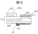
《端子部2》
図2は、本発明による有機EL表示装置の端子部の他の実施例を示す断面図で、図1(c)に対応した図となっている。
<<
FIG. 2 is a cross-sectional view showing another embodiment of the terminal portion of the organic EL display device according to the present invention and corresponds to FIG.
図1(c)の場合と比較して異なる構成は、図1(c)に示したように形成した補強板材PLTにおいて、その周辺に補強材EFを被着させていることにある。この補強材EFの材料としては、たとえば、エポキシ樹脂が用いられる。 A configuration different from the case of FIG. 1C is that a reinforcing material EF is attached to the periphery of the reinforcing plate PLT formed as shown in FIG. For example, an epoxy resin is used as the material of the reinforcing material EF.
有機EL表示装置の撓みによって、比較的撓み易いフレキシブル基板SUBと比較的撓み難い補強板材PLTとの界面にその周辺から剥離が生じ易いのを回避せんがためである。 This is because it is avoided that the organic EL display device is likely to be peeled off from the periphery at the interface between the flexible substrate SUB that is relatively flexible and the reinforcing plate PLT that is relatively difficult to bend.
このため、前記補強材EFは矩形状からなる補強板材PLTの各辺のうち、フレキシブル基板SUBの周辺に近接される一辺を除く他の三辺部に設けることが望ましい。しかし,図1(c)に示すように、有機EL表示装置の中央部側に指向する一辺、すなわち、前記端子群TMGの各端子TMの延在方向と平行となる辺を除いた残りの辺部のみに設けるようにしても有効であることはもちろんである。 For this reason, it is desirable that the reinforcing material EF is provided on the other three sides except for one side close to the periphery of the flexible substrate SUB among the sides of the rectangular reinforcing plate PLT. However, as shown in FIG. 1C, the remaining side excluding one side directed to the center side of the organic EL display device, that is, the side parallel to the extending direction of each terminal TM of the terminal group TMG. Of course, it is effective even if it is provided only in the section.
なお、前記補強材EFは、補強板材PLTの辺部において該辺とフレキシブル基板SUBとの境界部を含み、該辺およびフレキシブル基板SUBのいずれの側においても幅を有して被着されるようになっている。 The reinforcing material EF includes a boundary portion between the side and the flexible substrate SUB at the side portion of the reinforcing plate PLT, and is attached with a width on either side of the side or the flexible substrate SUB. It has become.
《端子部3》
図3は、本発明による有機EL表示装置の端子部の他の実施例を示す断面図で、図2に対応した図となっている。
<< Terminal part 3 >>
FIG. 3 is a cross-sectional view showing another embodiment of the terminal portion of the organic EL display device according to the present invention and corresponds to FIG.
図2の場合と比較して異なる構成は、補強板材PLTのフレキシブル基板SUBに対する補強とともに、フレキシブル配線基板PSBの前記積層体PILおよび封止剤SEALに対する補強をも行なった構成となっていることにある。 2 is different from the case of FIG. 2 in that the reinforcing plate material PLT is reinforced to the flexible substrate SUB and the flexible wiring substrate PSB is reinforced to the laminate PIL and the sealing agent SEAL. is there.
すなわち、前記補強板材PLTはフレキシブル配線基板PSBの剥離防止にあることから、該フレキシブル配線基板PSB自体にも剥離防止手段を設けたことにある。 That is, since the reinforcing plate PLT is for preventing peeling of the flexible wiring board PSB, the flexible wiring board PSB itself is also provided with peeling preventing means.
フレキシブル配線基板PSBの端子TMと接続される部分は、それに隣接して配置される他のフレキシブル配線基板PSBとの間、および封止剤SEALとの間に隙間を有し、これらの部分に第2補強材EF2を被着した構成とすることが望ましい。 The portions connected to the terminals TM of the flexible wiring board PSB have gaps between other flexible wiring boards PSB arranged adjacent to the terminals TM and the sealant SEAL. 2 It is desirable that the reinforcing material EF2 be applied.
しかし、この場合にあっても、前記補強板材PLTを補強する補強材EFの場合と同様、図3に示すように、封止剤SEALとの間にのみ第2補強材EF2を設けるようにしてもよい。 However, even in this case, as in the case of the reinforcing material EF that reinforces the reinforcing plate PLT, as shown in FIG. 3, the second reinforcing material EF2 is provided only between the sealant SEAL. Also good.
《端子部4》
図4は、本発明による有機EL表示装置の端子部の他の実施例を示す断面図で、図2に対応した図となっている。
<< Terminal 4 >>
FIG. 4 is a sectional view showing another embodiment of the terminal portion of the organic EL display device according to the present invention and corresponds to FIG.
図2の場合と比較して異なる構成は、フレキシブル基板SUBに被着する補強板材PLTは、端子が形成されている領域(互いに隣接する複数の端子のそれらを囲んだ領域)よりも若干大きく、換言すれば、該領域から外方へ広がる面積に対応する部分にまで及んで形成されていることにある。 The configuration different from the case of FIG. 2 is that the reinforcing plate PLT to be attached to the flexible substrate SUB is slightly larger than the region where the terminals are formed (the region surrounding a plurality of terminals adjacent to each other) In other words, it is formed so as to extend to a portion corresponding to an area extending outward from the region.
図2の場合、補強板材PLTは、端子の延在方向に沿って延在し、封止剤が形成されている面と充分対向できるまでに及んで形成されている。 In the case of FIG. 2, the reinforcing plate PLT extends along the extending direction of the terminal and is formed to the extent that it can sufficiently face the surface on which the sealing agent is formed.
《端子部5》
図5(a)は、本発明による有機EL表示装置の端子部の他の実施例を示す平面図で、図1(b)に対応した図となっている。
<< Terminal part 5 >>
FIG. 5A is a plan view showing another embodiment of the terminal portion of the organic EL display device according to the present invention, and corresponds to FIG.
図1(b)の場合と比較して異なる構成は、フレキシブル基板SUBの補強板材PLTを被着する面に第1アライメントマークAM1が形成され、また、前記補強板材PLTにも前記第1アライメントマークAM1と重なり合う第2アライメントマークAM2が形成されていることにある。 The configuration different from the case of FIG. 1B is that the first alignment mark AM1 is formed on the surface of the flexible substrate SUB on which the reinforcing plate material PLT is attached, and the first alignment mark is also formed on the reinforcing plate material PLT. The second alignment mark AM2 that overlaps AM1 is formed.
ここで、図5(b)において、フレキシブル基板SUBに形成された第1アライメントマークAM1を示し、図5(c)において、該フレキシブル基板SUBに被着される補強板材PLTに形成された第2アライメントマークAM2を示している。 Here, FIG. 5B shows the first alignment mark AM1 formed on the flexible substrate SUB. In FIG. 5C, the second alignment mark AM1 formed on the reinforcing plate PLT attached to the flexible substrate SUB. The alignment mark AM2 is shown.
このように構成することにより、補強板材PLTは互いに隣接する複数の端子に対して精度よい位置に補強板材PLTを被着でき、これにより、フレキシブル配線基板PSBの端子からの剥離を信頼性よく防止することができる。 By configuring in this way, the reinforcing plate PLT can be attached to the positions of the plurality of adjacent terminals with high accuracy, thereby reliably preventing the flexible wiring board PSB from being peeled off from the terminals. can do.
このことから、フレキシブル基板SUBに形成された第1アライメントマークAM1は、前記端子TMが形成されている積層体PILに対する位置決めのアライメントマークとして機能させるようにしてもよい。 Therefore, the first alignment mark AM1 formed on the flexible substrate SUB may function as an alignment mark for positioning with respect to the stacked body PIL on which the terminal TM is formed.
なお、第1アライメントマークAM1および第2アライメントマークAM2は、回転を含めた2次元配置に対する位置決めをするマークであることから、それぞれ、図5に示すように2個設けられている。また、それ以上の数であってもよいことはいうまでもない。 Since the first alignment mark AM1 and the second alignment mark AM2 are marks for positioning with respect to a two-dimensional arrangement including rotation, two are provided as shown in FIG. Needless to say, the number may be larger.
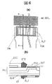
《端子部6》
図6(a)は、本発明による有機EL表示装置の端子部の他の実施例を示す平面図で、図1(b)に対応した図となっている。また、図6(a)のb−b線における断面図を図6(b)に示している。
<< Terminal part 6 >>
FIG. 6A is a plan view showing another embodiment of the terminal portion of the organic EL display device according to the present invention, and corresponds to FIG. A cross-sectional view taken along line bb in FIG. 6A is shown in FIG.
図1(b)の場合と比較して異なる構成は、フレキシブル基板SUBに被着される補強板材PLTは平板状ではなく、その中央部に孔が形成された環状体となっていることにある。有機EL表示装置において、その端子TMが形成された部分を他の部分よりも剛性を高くする趣旨から補強板材PLTの形状は必ずしも限定されることはないからである。 1B is different from the case of FIG. 1B in that the reinforcing plate PLT to be attached to the flexible substrate SUB is not a flat plate but an annular body having a hole formed in the center thereof. . This is because in the organic EL display device, the shape of the reinforcing plate PLT is not necessarily limited in order to make the portion where the terminal TM is formed more rigid than the other portions.
また、この実施例の場合は、図1に示したものと異なり、フレキシブル配線基板PSBと封止剤SEALとの間に補強材EFを被着させている。もちろん、この補強材EFは必ずしも被着させる必要のないものであることはいうまでもない。 Further, in the case of this embodiment, unlike the one shown in FIG. 1, the reinforcing material EF is adhered between the flexible wiring board PSB and the sealing agent SEAL. Of course, it goes without saying that the reinforcing material EF is not necessarily applied.
なお、上述のように環状体として形成した補強板材PLTのフレキシブル基板SUBへの被着を強化させる補強材EFは該補強板材PLTの外周部において被着させたものであるが、その開口の内周部にも被着させるようにしてもよいことはいうまでもない。補強板材PLTのフレキシブル基板SUBからの剥離の防止を強化せんがためである。 The reinforcing material EF that reinforces the adhesion of the reinforcing plate material PLT formed as an annular body to the flexible substrate SUB as described above is applied on the outer peripheral portion of the reinforcing plate material PLT. Needless to say, it may also be applied to the periphery. This is because the prevention of peeling of the reinforcing plate PLT from the flexible substrate SUB is strengthened.
また、前記補強板材PLTは、その中央部に開口が設けられた環状体である必要はなく、この開口の部分が周囲よりも剛性が弱い材料で充填された部材であってもよいことはいうまでもない。 Further, the reinforcing plate PLT need not be an annular body having an opening at the center, and may be a member filled with a material whose opening is less rigid than the surroundings. Not too long.
なお、上述した実施例では、有機EL表示装置について説明したものであるが、たとえば、液晶表示装置等の他の表示装置にも適用できることはいうまでもない。液晶表示装置の場合であっても、液晶を介して互いに対向配置されるフレキシブル基板を外囲器とし、該フレキシブル基板の液晶側の面に形成した電子回路の信号線を引き出すための端子を該フレキシブル基板の上側に設けて構成でき、事情は全く同じだからである。 In the above-described embodiments, the organic EL display device has been described. Needless to say, the present invention can also be applied to other display devices such as a liquid crystal display device. Even in the case of a liquid crystal display device, a flexible substrate that is disposed to face each other with a liquid crystal interposed therebetween is used as an envelope, and terminals for drawing out signal lines of an electronic circuit formed on the liquid crystal side surface of the flexible substrate are provided in the envelope. This is because it can be provided on the upper side of the flexible substrate and the situation is exactly the same.
上述した各実施例はそれぞれ単独に、あるいは組み合わせて用いても良い。それぞれの実施例での効果を単独であるいは相乗して奏することができるからである。 Each of the embodiments described above may be used alone or in combination. This is because the effects of the respective embodiments can be achieved independently or synergistically.
SUB……フレキシブル基板、AR……表示部、PIL……積層体、DSC……乾燥剤層、SEAL……封止剤、TM……端子、TMG……端子群、PSB……フレキシブル配線基板、ACF……異方性導電膜、PLT……補強板材、EF……補強材、EF2……第2補強材、AM1……第1アライメントマーク、AM2……第2アライメントマーク。 SUB: Flexible substrate, AR: Display unit, PIL: Laminate, DSC: Desiccant layer, SEAL: Sealant, TM ... Terminal, TMG ... Terminal group, PSB ... Flexible wiring board, ACF: anisotropic conductive film, PLT: reinforcing plate material, EF: reinforcing material , EF2: second reinforcing material , AM1: first alignment mark, AM2: second alignment mark.
Claims (11)
前記フレキシブル基板の一方の面に、信号を供給する端子群が形成され、
前記フレキシブル基板は、前記一方の面とは反対側の面で、且つ前記一方の面に形成された前記端子群と対向する領域に、補強部材が取り付けられ、
前記補強部材は前記端子群と絶縁され、
前記補強部材と前記端子群とが重なっている部分の剛性は、前記フレキシブル基板の内、前記補強部材と重なっていない部分の剛性よりも高いことを特徴とする表示装置。 A display device having a flexible substrate as at least a part of an envelope,
A terminal group for supplying a signal is formed on one surface of the flexible substrate,
The flexible substrate has a reinforcing member attached to a region opposite to the one surface and in a region facing the terminal group formed on the one surface,
The reinforcing member is insulated from the terminal group;
The display device according to claim 1, wherein a rigidity of a portion where the reinforcing member and the terminal group overlap is higher than a rigidity of a portion of the flexible substrate that does not overlap the reinforcing member.
前記フレキシブル基板の一方の面に、信号を供給する端子群が形成され、
前記端子群は、前記一方の面でフレキシブル配線基板と接続され、
前記フレキシブル基板は、前記一方の面とは反対側の面で、且つ前記一方の面に形成された前記端子群と対向する領域に、補強部材が取り付けられ、
前記補強部材と前記端子群とが重なっている部分の剛性は、前記フレキシブル基板の内、前記補強部材と重なっていない部分の剛性よりも高いことを特徴とする表示装置。 A display device having a flexible substrate as at least a part of an envelope,
A terminal group for supplying a signal is formed on one surface of the flexible substrate,
The terminal group is connected to the flexible wiring board on the one surface,
The flexible substrate has a reinforcing member attached to a region opposite to the one surface and in a region facing the terminal group formed on the one surface,
The display device according to claim 1, wherein a rigidity of a portion where the reinforcing member and the terminal group overlap is higher than a rigidity of a portion of the flexible substrate that does not overlap the reinforcing member.
複数の端子と、複数のフレキシブル配線基板と、複数の補強部材とを有し、
前記複数の端子は、前記フレキシブル基板の一方の面に形成され、
前記複数の端子は、前記複数の端子のうちの互いに隣接し合う複数本で形成される複数の端子群に分けられ、
前記複数の端子群の各々は、前記一方の面で前記複数のフレキシブル配線基板の各々と接続され、
前記フレキシブル基板は、前記一方の面とは反対側の面で、且つ前記複数の端子群と対向する各々の領域に、前記複数の補強部材の各々が取り付けられ、
前記複数の補強部材の各々と前記複数の端子群の各々とが重なっている部分の剛性は、前記フレキシブル基板の内、前記補強部材と重なっていない部分の剛性よりも高いことを特徴とする表示装置。 A display device having a flexible substrate as at least a part of an envelope,
Having a plurality of terminals, a plurality of flexible wiring boards, and a plurality of reinforcing members;
The plurality of terminals are formed on one surface of the flexible substrate,
The plurality of terminals are divided into a plurality of terminal groups formed by a plurality of adjacent ones of the plurality of terminals,
Each of the plurality of terminal groups is connected to each of the plurality of flexible wiring boards on the one surface,
Each of the plurality of reinforcing members is attached to each region of the flexible substrate on a surface opposite to the one surface and facing the plurality of terminal groups,
The rigidity of the portion where each of the plurality of reinforcing members and each of the plurality of terminal groups overlap is higher than the rigidity of the portion of the flexible substrate that does not overlap with the reinforcing member. apparatus.
前記フレキシブル基板の前記複数の端子群が形成されている層と、前記複数のフレキシブル配線基板の少なくとも一つとに跨って、塗布形成された補強材とを有することを特徴とする請求項5に記載の表示装置。 An anisotropic conductive film connecting each of the plurality of flexible wiring boards and each of the plurality of terminal groups;
6. The reinforcing board according to claim 5, further comprising: a layer on which the plurality of terminal groups of the flexible substrate are formed, and a reinforcing material applied and formed across at least one of the plurality of flexible wiring boards. Display device.
Priority Applications (3)
| Application Number | Priority Date | Filing Date | Title |
|---|---|---|---|
| JP2003357882A JP4627140B2 (en) | 2003-10-17 | 2003-10-17 | Display device |
| US10/964,667 US7359215B2 (en) | 2003-10-17 | 2004-10-15 | Flexible display device |
| CNB200410080784XA CN100555654C (en) | 2003-10-17 | 2004-10-15 | Flexible display apparatus |
Applications Claiming Priority (1)
| Application Number | Priority Date | Filing Date | Title |
|---|---|---|---|
| JP2003357882A JP4627140B2 (en) | 2003-10-17 | 2003-10-17 | Display device |
Publications (3)
| Publication Number | Publication Date |
|---|---|
| JP2005121965A JP2005121965A (en) | 2005-05-12 |
| JP2005121965A5 JP2005121965A5 (en) | 2006-11-02 |
| JP4627140B2 true JP4627140B2 (en) | 2011-02-09 |
Family
ID=34587164
Family Applications (1)
| Application Number | Title | Priority Date | Filing Date |
|---|---|---|---|
| JP2003357882A Expired - Lifetime JP4627140B2 (en) | 2003-10-17 | 2003-10-17 | Display device |
Country Status (3)
| Country | Link |
|---|---|
| US (1) | US7359215B2 (en) |
| JP (1) | JP4627140B2 (en) |
| CN (1) | CN100555654C (en) |
Families Citing this family (23)
| Publication number | Priority date | Publication date | Assignee | Title |
|---|---|---|---|---|
| US20050253511A1 (en) * | 2004-05-11 | 2005-11-17 | World Properties, Inc. | Flexible EL lamp with reinforced leads |
| US7638888B2 (en) * | 2007-02-16 | 2009-12-29 | Panasonic Corporation | Semiconductor chip mounting substrate, semiconductor chip mounting body, semiconductor chip stacked module, and semiconductor chip mounting substrate manufacturing method |
| JP5437567B2 (en) * | 2007-07-10 | 2014-03-12 | ゴールドチャームリミテッド | LCD module |
| TWI360376B (en) | 2008-04-11 | 2012-03-11 | E Ink Holdings Inc | Flexible display apparatus |
| JP5399683B2 (en) * | 2008-10-24 | 2014-01-29 | 株式会社ジャパンディスプレイ | Display device and electronic device |
| JP4853531B2 (en) * | 2009-03-04 | 2012-01-11 | 富士ゼロックス株式会社 | Display media |
| CN105659310B (en) | 2013-08-13 | 2021-02-26 | 飞利斯有限公司 | Optimization of electronic display area |
| WO2015031426A1 (en) | 2013-08-27 | 2015-03-05 | Polyera Corporation | Flexible display and detection of flex state |
| CN105793781B (en) | 2013-08-27 | 2019-11-05 | 飞利斯有限公司 | Attachable device with deflection electronic component |
| WO2015038684A1 (en) | 2013-09-10 | 2015-03-19 | Polyera Corporation | Attachable article with signaling, split display and messaging features |
| EP3087559B1 (en) | 2013-12-24 | 2021-05-05 | Flexterra, Inc. | Support structures for a flexible electronic component |
| CN106031308B (en) | 2013-12-24 | 2019-08-09 | 飞利斯有限公司 | Support construction for attachment two dimension flexible electrical device |
| WO2015100224A1 (en) | 2013-12-24 | 2015-07-02 | Polyera Corporation | Flexible electronic display with user interface based on sensed movements |
| TWI653522B (en) | 2013-12-24 | 2019-03-11 | 美商飛利斯有限公司 | Dynamic flexible article |
| US20150227245A1 (en) | 2014-02-10 | 2015-08-13 | Polyera Corporation | Attachable Device with Flexible Electronic Display Orientation Detection |
| JP6141794B2 (en) * | 2014-05-21 | 2017-06-07 | 日本発條株式会社 | Terminal connection structure |
| WO2015184045A2 (en) | 2014-05-28 | 2015-12-03 | Polyera Corporation | Device with flexible electronic components on multiple surfaces |
| CN104167429B (en) * | 2014-08-01 | 2017-05-31 | 京东方科技集团股份有限公司 | A kind of flexible display panels and preparation method thereof, display device |
| WO2016138356A1 (en) | 2015-02-26 | 2016-09-01 | Polyera Corporation | Attachable device having a flexible electronic component |
| KR102387786B1 (en) * | 2015-07-28 | 2022-04-15 | 엘지디스플레이 주식회사 | Backplane Substrate and Flexible Display Using the Same |
| KR102554290B1 (en) | 2016-05-23 | 2023-07-13 | 삼성디스플레이 주식회사 | Display device |
| KR102636736B1 (en) * | 2016-09-08 | 2024-02-15 | 삼성디스플레이 주식회사 | Display device |
| WO2020065856A1 (en) * | 2018-09-27 | 2020-04-02 | シャープ株式会社 | Method for manufacturing display device |
Citations (7)
| Publication number | Priority date | Publication date | Assignee | Title |
|---|---|---|---|---|
| JPH0277018A (en) * | 1988-09-13 | 1990-03-16 | Optrex Corp | Electrooptical device and method for connecting this device |
| JPH02127620A (en) * | 1988-11-08 | 1990-05-16 | Optrex Corp | Electrooptic device and its connecting method |
| JPH02253591A (en) * | 1989-03-27 | 1990-10-12 | Hitachi Maxell Ltd | Dispersion type el element furnished with flexible printed substrate |
| JPH03184077A (en) * | 1989-12-13 | 1991-08-12 | Fujitsu Ltd | Terminal processing structure for flat display panel |
| JPH07140479A (en) * | 1993-11-22 | 1995-06-02 | Fujitsu Ltd | Lcd unit |
| JPH07175059A (en) * | 1993-12-16 | 1995-07-14 | Casio Comput Co Ltd | Liquid crystal display device and terminal connecting structure thereof |
| JP2003258396A (en) * | 2002-02-28 | 2003-09-12 | Seiko Epson Corp | Electronic device and method of manufacturing the same, semiconductor device and electronic equipment |
Family Cites Families (10)
| Publication number | Priority date | Publication date | Assignee | Title |
|---|---|---|---|---|
| JPH10177894A (en) | 1996-12-19 | 1998-06-30 | Matsushita Electric Ind Co Ltd | Distributed-electroluminescent element board |
| JPH1187754A (en) | 1997-09-08 | 1999-03-30 | Fuji Electric Co Ltd | Method for connecting outer lead of solar battery module |
| JP3804269B2 (en) | 1998-03-31 | 2006-08-02 | カシオ計算機株式会社 | Flexible wiring board bonding structure |
| JP2001210998A (en) | 2000-01-21 | 2001-08-03 | Denso Corp | Method for mounting flexible substrate and reinforcing board used therefor |
| US6819304B2 (en) * | 2001-10-11 | 2004-11-16 | International Business Machines Corporation | Adjustable display device with display adjustment function and method therefor |
| TWI264121B (en) * | 2001-11-30 | 2006-10-11 | Semiconductor Energy Lab | A display device, a method of manufacturing a semiconductor device, and a method of manufacturing a display device |
| US6953735B2 (en) * | 2001-12-28 | 2005-10-11 | Semiconductor Energy Laboratory Co., Ltd. | Method for fabricating a semiconductor device by transferring a layer to a support with curvature |
| US7242398B2 (en) * | 2002-02-18 | 2007-07-10 | Ignis Innovation Inc. | Flexible display device |
| JP3908059B2 (en) * | 2002-02-27 | 2007-04-25 | スター精密株式会社 | Electret condenser microphone |
| US6885146B2 (en) * | 2002-03-14 | 2005-04-26 | Semiconductor Energy Laboratory Co., Ltd. | Display device comprising substrates, contrast medium and barrier layers between contrast medium and each of substrates |
-
2003
- 2003-10-17 JP JP2003357882A patent/JP4627140B2/en not_active Expired - Lifetime
-
2004
- 2004-10-15 CN CNB200410080784XA patent/CN100555654C/en active Active
- 2004-10-15 US US10/964,667 patent/US7359215B2/en active Active
Patent Citations (7)
| Publication number | Priority date | Publication date | Assignee | Title |
|---|---|---|---|---|
| JPH0277018A (en) * | 1988-09-13 | 1990-03-16 | Optrex Corp | Electrooptical device and method for connecting this device |
| JPH02127620A (en) * | 1988-11-08 | 1990-05-16 | Optrex Corp | Electrooptic device and its connecting method |
| JPH02253591A (en) * | 1989-03-27 | 1990-10-12 | Hitachi Maxell Ltd | Dispersion type el element furnished with flexible printed substrate |
| JPH03184077A (en) * | 1989-12-13 | 1991-08-12 | Fujitsu Ltd | Terminal processing structure for flat display panel |
| JPH07140479A (en) * | 1993-11-22 | 1995-06-02 | Fujitsu Ltd | Lcd unit |
| JPH07175059A (en) * | 1993-12-16 | 1995-07-14 | Casio Comput Co Ltd | Liquid crystal display device and terminal connecting structure thereof |
| JP2003258396A (en) * | 2002-02-28 | 2003-09-12 | Seiko Epson Corp | Electronic device and method of manufacturing the same, semiconductor device and electronic equipment |
Also Published As
| Publication number | Publication date |
|---|---|
| CN1610458A (en) | 2005-04-27 |
| CN100555654C (en) | 2009-10-28 |
| US20050110785A1 (en) | 2005-05-26 |
| US7359215B2 (en) | 2008-04-15 |
| JP2005121965A (en) | 2005-05-12 |
Similar Documents
| Publication | Publication Date | Title |
|---|---|---|
| JP4627140B2 (en) | Display device | |
| US11991913B2 (en) | Semiconductor device including detection electrodes applicable for a touch sensor | |
| CN107039495B (en) | Organic light emitting display panel and organic light emitting display device | |
| US8847246B2 (en) | Organic light emitting diode display | |
| CN107785394B (en) | Display device | |
| KR101699911B1 (en) | Organic light emitting diode display | |
| US9178175B2 (en) | Display device | |
| CN113920943A (en) | Display device and manufacturing method thereof | |
| US8421353B2 (en) | Organic light emitting diode display with specific sealing member | |
| JP2018116236A (en) | Display divice | |
| KR20120077471A (en) | Organic light emitting diode display and manufacturing method thereof | |
| US8692346B2 (en) | Metal encapsulating sheet and organic light-emitting display apparatus including the same | |
| TWI619244B (en) | Organic light emitting diode display | |
| KR102055194B1 (en) | Display Apparatus | |
| KR20190052327A (en) | Display device | |
| US9337440B2 (en) | Organic luminescent display device | |
| JP2005128040A (en) | Display device | |
| JP2004200041A (en) | Organic el display device | |
| JP4209744B2 (en) | Organic EL display device | |
| CN110072309B (en) | Light emitting device | |
| US20210343826A1 (en) | Display device | |
| JP2018106803A (en) | Organic el display device and method of manufacturing organic el display device | |
| JP4606480B2 (en) | Organic EL display device | |
| JP2006004731A (en) | Organic el display device and its manufacturing method |
Legal Events
| Date | Code | Title | Description |
|---|---|---|---|
| A521 | Request for written amendment filed |
Free format text: JAPANESE INTERMEDIATE CODE: A523 Effective date: 20060915 |
|
| A621 | Written request for application examination |
Free format text: JAPANESE INTERMEDIATE CODE: A621 Effective date: 20060915 |
|
| A977 | Report on retrieval |
Free format text: JAPANESE INTERMEDIATE CODE: A971007 Effective date: 20100128 |
|
| A131 | Notification of reasons for refusal |
Free format text: JAPANESE INTERMEDIATE CODE: A131 Effective date: 20100202 |
|
| A521 | Request for written amendment filed |
Free format text: JAPANESE INTERMEDIATE CODE: A523 Effective date: 20100325 |
|
| A131 | Notification of reasons for refusal |
Free format text: JAPANESE INTERMEDIATE CODE: A131 Effective date: 20100824 |
|
| A521 | Request for written amendment filed |
Free format text: JAPANESE INTERMEDIATE CODE: A523 Effective date: 20101018 |
|
| TRDD | Decision of grant or rejection written | ||
| A01 | Written decision to grant a patent or to grant a registration (utility model) |
Free format text: JAPANESE INTERMEDIATE CODE: A01 Effective date: 20101102 |
|
| A01 | Written decision to grant a patent or to grant a registration (utility model) |
Free format text: JAPANESE INTERMEDIATE CODE: A01 |
|
| A61 | First payment of annual fees (during grant procedure) |
Free format text: JAPANESE INTERMEDIATE CODE: A61 Effective date: 20101104 |
|
| FPAY | Renewal fee payment (event date is renewal date of database) |
Free format text: PAYMENT UNTIL: 20131119 Year of fee payment: 3 |
|
| R150 | Certificate of patent or registration of utility model |
Ref document number: 4627140 Country of ref document: JP Free format text: JAPANESE INTERMEDIATE CODE: R150 Free format text: JAPANESE INTERMEDIATE CODE: R150 |
|
| FPAY | Renewal fee payment (event date is renewal date of database) |
Free format text: PAYMENT UNTIL: 20131119 Year of fee payment: 3 |
|
| S111 | Request for change of ownership or part of ownership |
Free format text: JAPANESE INTERMEDIATE CODE: R313121 Free format text: JAPANESE INTERMEDIATE CODE: R313115 |
|
| FPAY | Renewal fee payment (event date is renewal date of database) |
Free format text: PAYMENT UNTIL: 20131119 Year of fee payment: 3 |
|
| R350 | Written notification of registration of transfer |
Free format text: JAPANESE INTERMEDIATE CODE: R350 |
|
| R250 | Receipt of annual fees |
Free format text: JAPANESE INTERMEDIATE CODE: R250 |
|
| R250 | Receipt of annual fees |
Free format text: JAPANESE INTERMEDIATE CODE: R250 |
|
| R250 | Receipt of annual fees |
Free format text: JAPANESE INTERMEDIATE CODE: R250 |
|
| R250 | Receipt of annual fees |
Free format text: JAPANESE INTERMEDIATE CODE: R250 |
|
| R250 | Receipt of annual fees |
Free format text: JAPANESE INTERMEDIATE CODE: R250 |
|
| R250 | Receipt of annual fees |
Free format text: JAPANESE INTERMEDIATE CODE: R250 |
|
| S531 | Written request for registration of change of domicile |
Free format text: JAPANESE INTERMEDIATE CODE: R313531 |
|
| S533 | Written request for registration of change of name |
Free format text: JAPANESE INTERMEDIATE CODE: R313533 |
|
| S111 | Request for change of ownership or part of ownership |
Free format text: JAPANESE INTERMEDIATE CODE: R313113 |
|
| R350 | Written notification of registration of transfer |
Free format text: JAPANESE INTERMEDIATE CODE: R350 |
|
| R350 | Written notification of registration of transfer |
Free format text: JAPANESE INTERMEDIATE CODE: R350 |
|
| R250 | Receipt of annual fees |
Free format text: JAPANESE INTERMEDIATE CODE: R250 |
|
| R250 | Receipt of annual fees |
Free format text: JAPANESE INTERMEDIATE CODE: R250 |
|
| R250 | Receipt of annual fees |
Free format text: JAPANESE INTERMEDIATE CODE: R250 |
|
| R250 | Receipt of annual fees |
Free format text: JAPANESE INTERMEDIATE CODE: R250 |
|
| EXPY | Cancellation because of completion of term |