JP4627078B2 - DIGITAL / ANALOG CONVERSION CIRCUIT, DATA DRIVER AND DISPLAY DEVICE - Google Patents
DIGITAL / ANALOG CONVERSION CIRCUIT, DATA DRIVER AND DISPLAY DEVICE Download PDFInfo
- Publication number
- JP4627078B2 JP4627078B2 JP2007277710A JP2007277710A JP4627078B2 JP 4627078 B2 JP4627078 B2 JP 4627078B2 JP 2007277710 A JP2007277710 A JP 2007277710A JP 2007277710 A JP2007277710 A JP 2007277710A JP 4627078 B2 JP4627078 B2 JP 4627078B2
- Authority
- JP
- Japan
- Prior art keywords
- voltage
- reference voltage
- input
- voltages
- circuit
- Prior art date
- Legal status (The legal status is an assumption and is not a legal conclusion. Google has not performed a legal analysis and makes no representation as to the accuracy of the status listed.)
- Expired - Fee Related
Links
Images

Classifications
-
- G—PHYSICS
- G09—EDUCATION; CRYPTOGRAPHY; DISPLAY; ADVERTISING; SEALS
- G09G—ARRANGEMENTS OR CIRCUITS FOR CONTROL OF INDICATING DEVICES USING STATIC MEANS TO PRESENT VARIABLE INFORMATION
- G09G3/00—Control arrangements or circuits, of interest only in connection with visual indicators other than cathode-ray tubes
- G09G3/20—Control arrangements or circuits, of interest only in connection with visual indicators other than cathode-ray tubes for presentation of an assembly of a number of characters, e.g. a page, by composing the assembly by combination of individual elements arranged in a matrix no fixed position being assigned to or needed to be assigned to the individual characters or partial characters
- G09G3/34—Control arrangements or circuits, of interest only in connection with visual indicators other than cathode-ray tubes for presentation of an assembly of a number of characters, e.g. a page, by composing the assembly by combination of individual elements arranged in a matrix no fixed position being assigned to or needed to be assigned to the individual characters or partial characters by control of light from an independent source
- G09G3/36—Control arrangements or circuits, of interest only in connection with visual indicators other than cathode-ray tubes for presentation of an assembly of a number of characters, e.g. a page, by composing the assembly by combination of individual elements arranged in a matrix no fixed position being assigned to or needed to be assigned to the individual characters or partial characters by control of light from an independent source using liquid crystals
- G09G3/3611—Control of matrices with row and column drivers
- G09G3/3685—Details of drivers for data electrodes
- G09G3/3688—Details of drivers for data electrodes suitable for active matrices only
-
- H—ELECTRICITY
- H03—ELECTRONIC CIRCUITRY
- H03M—CODING; DECODING; CODE CONVERSION IN GENERAL
- H03M1/00—Analogue/digital conversion; Digital/analogue conversion
- H03M1/66—Digital/analogue converters
- H03M1/661—Improving the reconstruction of the analogue output signal beyond the resolution of the digital input signal, e.g. by interpolation, by curve-fitting, by smoothing
-
- G—PHYSICS
- G09—EDUCATION; CRYPTOGRAPHY; DISPLAY; ADVERTISING; SEALS
- G09G—ARRANGEMENTS OR CIRCUITS FOR CONTROL OF INDICATING DEVICES USING STATIC MEANS TO PRESENT VARIABLE INFORMATION
- G09G2310/00—Command of the display device
- G09G2310/02—Addressing, scanning or driving the display screen or processing steps related thereto
- G09G2310/0264—Details of driving circuits
- G09G2310/027—Details of drivers for data electrodes, the drivers handling digital grey scale data, e.g. use of D/A converters
-
- H—ELECTRICITY
- H03—ELECTRONIC CIRCUITRY
- H03M—CODING; DECODING; CODE CONVERSION IN GENERAL
- H03M1/00—Analogue/digital conversion; Digital/analogue conversion
- H03M1/66—Digital/analogue converters
- H03M1/68—Digital/analogue converters with conversions of different sensitivity, i.e. one conversion relating to the more significant digital bits and another conversion to the less significant bits
-
- H—ELECTRICITY
- H03—ELECTRONIC CIRCUITRY
- H03M—CODING; DECODING; CODE CONVERSION IN GENERAL
- H03M1/00—Analogue/digital conversion; Digital/analogue conversion
- H03M1/66—Digital/analogue converters
- H03M1/74—Simultaneous conversion
- H03M1/76—Simultaneous conversion using switching tree
Landscapes
- Engineering & Computer Science (AREA)
- Theoretical Computer Science (AREA)
- Chemical & Material Sciences (AREA)
- Crystallography & Structural Chemistry (AREA)
- Physics & Mathematics (AREA)
- Computer Hardware Design (AREA)
- General Physics & Mathematics (AREA)
- Liquid Crystal Display Device Control (AREA)
- Control Of Indicators Other Than Cathode Ray Tubes (AREA)
- Analogue/Digital Conversion (AREA)
- Liquid Crystal (AREA)
Description
本発明は、デジタルアナログ変換回路とデータドライバ及びそれを用いた表示装置に関する。 The present invention relates to a digital-analog conversion circuit, a data driver, and a display device using the same.
近時、表示装置は、薄型、軽量、低消費電力を特徴とする液晶表示装置(LCD)が幅広く普及し、携帯電話機(モバイルフォン、セルラフォン)やPDA(パーソナルデジタルアシスタント)、ノートPC等のモバイル機器の表示部に多く利用されてきた。しかし最近では液晶表示装置の大画面化や動画対応の技術も高まり、モバイル用途だけでなく据置型の大画面表示装置や大画面液晶テレビも実現可能になってきている。これらの液晶表示装置としては、高精細表示が可能なアクティブマトリクス駆動方式の液晶表示装置が利用されている。 Recently, liquid crystal display devices (LCD) characterized by thinness, light weight, and low power consumption have been widely used as display devices, and mobile phones such as mobile phones (mobile phones, cellular phones), PDAs (personal digital assistants), and notebook PCs. It has been widely used in the display section of equipment. Recently, however, the technology for increasing the screen size of liquid crystal display devices and moving images has been increasing, and not only mobile applications but also stationary large screen display devices and large screen liquid crystal televisions can be realized. As these liquid crystal display devices, active matrix drive type liquid crystal display devices capable of high-definition display are used.
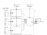
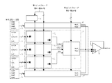
はじめに、図21を参照して、アクティブマトリクス駆動方式の液晶表示装置の典型的な構成について概説しておく。なお、図21には、液晶表示部の1画素に接続される主要な構成が、等価回路によって模式的に示されている。 First, a typical configuration of an active matrix drive type liquid crystal display device will be outlined with reference to FIG. In FIG. 21, the main configuration connected to one pixel of the liquid crystal display unit is schematically shown by an equivalent circuit.
一般に、アクティブマトリクス駆動方式の液晶表示装置の表示部960は、透明な画素電極964及び薄膜トランジスタ(TFT)963をマトリックス状に配置した半導体基板(例えばカラーSXGAパネルの場合、1280×3画素列×1024画素行)と、面全体に1つの透明な電極967を形成した対向基板と、これら2枚の基板を対向させて間に液晶を封入した構造からなる。液晶は容量性を有し、画素電極964と電極967との間に容量965をなす。また、液晶の容量性を補助するための補助容量966を更に備えることが多い。 In general, a display unit 960 of an active matrix liquid crystal display device includes a semiconductor substrate in which transparent pixel electrodes 964 and thin film transistors (TFTs) 963 are arranged in a matrix (for example, in the case of a color SXGA panel, 1280 × 3 pixel columns × 1024). A pixel row), a counter substrate in which one transparent electrode 967 is formed on the entire surface, and a structure in which liquid crystal is sealed between the two substrates facing each other. The liquid crystal has capacitance, and a capacitor 965 is formed between the pixel electrode 964 and the electrode 967. In many cases, an auxiliary capacitor 966 for assisting the capacitive property of the liquid crystal is further provided.
上記液晶表示装置は、スイッチング機能を持つTFT963のオン・オフを走査信号により制御し、TFT963がオンとなるときに、映像データ信号に対応した階調信号電圧が画素電極964に印加され、各画素電極964と対向基板電極967との間の電位差により液晶の透過率が変化し、TFT963がオフとされた後も該電位差を液晶容量965及び補助容量966で一定期間保持することで画像を表示するものである。 The liquid crystal display device controls on / off of the TFT 963 having a switching function by a scanning signal, and when the TFT 963 is turned on, a gradation signal voltage corresponding to the video data signal is applied to the pixel electrode 964, and each pixel The transmittance of the liquid crystal changes due to the potential difference between the electrode 964 and the counter substrate electrode 967, and an image is displayed by holding the potential difference for a certain period in the liquid crystal capacitor 965 and the auxiliary capacitor 966 even after the TFT 963 is turned off. Is.
半導体基板上には、各画素電極964へ印加する複数のレベル電圧(階調信号電圧)を送るデータ線962と、走査信号を送る走査線961とが格子状に配線され(上記カラーSXGAパネルの場合、データ線は1280×3本、走査線は1024本)、走査線961及びデータ線962は、互いの交差部に生じる容量や対向基板電極との間に挟まれる液晶容量等により、大きな容量性負荷となっている。 On the semiconductor substrate, data lines 962 for sending a plurality of level voltages (gradation signal voltages) to be applied to the pixel electrodes 964 and scanning lines 961 for sending scanning signals are wired in a grid pattern (in the color SXGA panel). In this case, the number of data lines is 1280 × 3 and the number of scanning lines is 1024), and the scanning lines 961 and the data lines 962 have a large capacity due to the capacity generated at the intersection or the liquid crystal capacity sandwiched between the counter substrate electrodes. Sexual load.
なお、走査信号はゲートドライバ970より走査線961に供給され、また各画素電極964への階調信号電圧の供給はデータドライバ980よりデータ線962を介して行われる。またゲートドライバ970及びデータドライバ980は、表示コントローラー950によって制御され、それぞれ必要なクロックCLK、制御信号等が表示コントローラー950より供給され、映像データは、データドライバ980に供給される。なお現在では、映像データはデジタルデータが主流となっている。電源回路940は、ゲートドライバ970、データドライバ980に駆動電源を供給する。 Note that the scanning signal is supplied from the gate driver 970 to the scanning line 961, and the gradation signal voltage is supplied to each pixel electrode 964 from the data driver 980 through the data line 962. The gate driver 970 and the data driver 980 are controlled by the display controller 950, and necessary clocks CLK, control signals, and the like are supplied from the display controller 950, and video data is supplied to the data driver 980. At present, video data is mainly digital data. The power supply circuit 940 supplies driving power to the gate driver 970 and the data driver 980.
1画面分のデータの書き換えは、1フレーム期間(1/60・秒)で行われ、各走査線で1画素行毎(ライン毎)、順次、選択され、選択期間内に、各データ線より階調信号電圧が供給される。 Rewriting of data for one screen is performed in one frame period (1/60 · sec), and is sequentially selected for each pixel line (each line) in each scanning line. A gradation signal voltage is supplied.
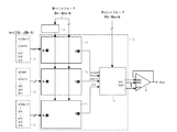
ゲートドライバ970は、少なくとも2値の走査信号を供給すればよいのに対し、データドライバ980は、データ線を階調数に応じた多値レベルの階調信号電圧で駆動することが必要とされる。このため、データドライバ980は、映像データを階調信号電圧に変換するデコーダと、その階調信号電圧をデータ線962に増幅出力する演算増幅器を含むデジタルアナログ変換回路(DAC)を備えている。 The gate driver 970 only needs to supply at least a binary scanning signal, whereas the data driver 980 is required to drive the data line with a multi-level gradation signal voltage corresponding to the number of gradations. The Therefore, the data driver 980 includes a digital / analog conversion circuit (DAC) including a decoder that converts video data into a gradation signal voltage, and an operational amplifier that amplifies and outputs the gradation signal voltage to the data line 962.
携帯電話端末、ノートPC、モニタ、液晶TV等において、高画質化(多色化)が進んでいる。少なくともRGB各6ビット映像データ(26万色)、さらには8ビット映像データ(2680万色)以上の需要が高まっている。 In mobile phone terminals, notebook PCs, monitors, liquid crystal TVs, and the like, image quality (multicolor) is increasing. There is a growing demand for at least 6-bit RGB RGB data (260,000 colors), and more than 8-bit video data (26.8 million colors).
このため、多ビット映像データに対応した階調信号電圧を出力するデータドライバは、多階調電圧出力とともに、階調に対応した非常に高精度な電圧出力が求められるようになってきている。多階調電圧に対応して発生する参照電圧(基準電圧)を増大させると、参照電圧発生回路の素子数、入力映像信号に対応した参照電圧を選択するデコーダ回路のスイッチトランジスタの素子数を増大させることになる。 For this reason, data drivers that output gradation signal voltages corresponding to multi-bit video data are required to output voltage with very high accuracy corresponding to gradations in addition to multi-gradation voltage output. When the reference voltage (reference voltage) generated corresponding to the multi-gradation voltage is increased, the number of elements of the reference voltage generation circuit and the number of elements of the switch transistor of the decoder circuit for selecting the reference voltage corresponding to the input video signal are increased. I will let you.
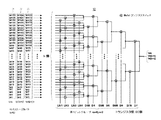
後記特許文献1には、内挿技術を利用して、参照電圧数及びスイッチトランジスタ数を削減する技術が提案されている。図23は、特許文献1(図10)に開示されるデータドライバのデジタルアナログ変換回路の選択回路の構成を示す図である。この構成は、2入力の出力アンプ回路(内挿アンプ)を用いる。内挿アンプには、OUT1(Vn)、OUT2(Vn+2)が入力され、2つの入力を1:1に内分した電圧を出力する。入力8ビットを6ビットと2ビットに分割し、6ビットの信号をデコードするデコーダにトーナメント方式のデコーダ(トーナメント1、2、3)を用いている。8ビットの表示データについて、6ビット(D0P、D0N、D1P、D1N、D2P、D2N、D3P、D3N、D4P、D4N、D5P、D5N)の入力階調を次の3つのブロック(A、B、C)に分割する。
V(0)、V(8)、・・・V(0+8n)、・・・V(248)、V(256)を、トーナメント1でデコードする。V(2)、V(6)、V(2+4n)、・・・V(250)、V(254)をトーナメント2でデコードする。V(4)、V(4+8n)、・・・、V(252)をトーナメント3でデコードする。
V (0), V (8),... V (0 + 8n),... V (248), V (256) are decoded by
トーナメント1、トーナメント2およびトーナメント3で6ビット入力の第1のデコーダ(1stデコーダ)を構成する。
第1のデコーダの出力VA、VB、VCはD0N、D0Pを切換え信号とする選択回路を通して2ビット(D6P、D6N、D7P、D7N)の第2のデコーダ(2ndデコーダ)に入力され、2つの出力OUT1(Vn)、OUT2(Vn+2)を得ている。なお、D0N、D0Pは、1stデコーダと2ndデコーダの両方に入力されている。 Outputs VA, VB, and VC of the first decoder are input to a 2-bit (D6P, D6N, D7P, D7N) second decoder (2nd decoder) through a selection circuit using D0N and D0P as switching signals, and two outputs are output. OUT1 (Vn) and OUT2 (Vn + 2) are obtained. Note that D0N and D0P are input to both the 1st decoder and the 2nd decoder.
選択回路は、トーナメント1、2、3の出力VA、VB、VCのそれぞれから1つの出力を選択して、第2デコーダに入力する。
The selection circuit selects one output from each of the outputs VA, VB, and VC of the
第2デコーダの2つの出力OUT1(Vn)、OUT2(Vn+2)は、不図示の2入力の出力アンプ回路(内挿アンプ)に入力される。 Two outputs OUT1 (Vn) and OUT2 (Vn + 2) of the second decoder are input to a two-input output amplifier circuit (interpolation amplifier) (not shown).
この回路は、内挿アンプを用いて、参照電圧(階調電圧)の数を約1/2とするものである。 This circuit uses an interpolation amplifier to reduce the number of reference voltages (grayscale voltages) to about ½.
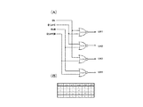
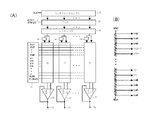
図24(A)は、図23におけるトーナメント1の構成を示す図であり、図24(B)はトーナメント3の構成を示す図である。図24(A)において、トーナメント1では、階調電圧0+8n(V00、V08、V16、・・・V248、V256)を入力し、6ビットの表示データ(D0P、D0N、D1P、D1N、D2P、D2N、D3P、D3N、D4P、D4N、D5P、D5N)をデコードして出力VAを得る。トーナメント2では、階調電圧2+4n(2、6、10、14、・・・250、254)を入力し、6ビットの表示データ(D0P、D0N、D1P、D1N、D2P、D2N、D3P、D3N、D4P、D4N、D5P、D5N)をデコードして出力VBを得る。トーナメント3では、階調電圧4+8n(V04、V12、V20、・・・V244、V252)を入力し、5ビットの表示データ(D1P、D1N、D2P、D2N、D3P、D3N、D4P、D4N、D5P、D5N)をデコードして出力VCを得る。
FIG. 24A is a diagram illustrating the configuration of the
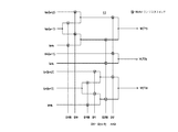
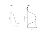
なお、データドライバは、通常、液晶の劣化を防ぐため、液晶パネルの対向基板電極の電圧VCOMに対して、正と負の電圧を交互に印加する交流駆動が行われる。そのため、正極駆動と負極駆動の階調電圧信号が出力される。図22(A)は、ノーマリホワイトの液晶における印加電圧と透過率の関係を示す図である。図22(B)は、図22(A)の特性をもつ液晶を駆動する液晶表示装置の階調とデータドライバの出力電圧(液晶の印加電圧)の関係を示す図である。図22(B)では、0階調で液晶印加電圧が最も高いとき、透過率が最も低く(黒表示)、階調が上がるにつれて液晶印加電圧が低下し、透過率は上昇し、白表示に近づく。液晶印加電圧と透過率の関係及び階調とデータドライバの出力電圧の関係は、図22(A)、(B)に示すように非線形な特性になっている。正極駆動におけるデータドライバの出力電圧は、例えば、階調255(8ビット)に対応したVCOMから階調0に対応した高位側電源電圧VDDまでの範囲とされ、負極駆動では、データドライバの出力電圧は、階調255に対応してVCOMから階調0に対応した低位側電源電圧(負電源電圧)VSSまでの範囲とされる。 Note that the data driver normally performs AC driving in which positive and negative voltages are alternately applied to the voltage VCOM of the counter substrate electrode of the liquid crystal panel in order to prevent deterioration of the liquid crystal. For this reason, grayscale voltage signals for positive polarity driving and negative polarity driving are output. FIG. 22A is a diagram illustrating a relationship between applied voltage and transmittance in normally white liquid crystal. FIG. 22B is a diagram showing the relationship between the gradation of the liquid crystal display device that drives the liquid crystal having the characteristics of FIG. 22A and the output voltage of the data driver (applied voltage of the liquid crystal). In FIG. 22B, when the liquid crystal applied voltage is the highest at the 0th gradation, the transmittance is the lowest (black display), the liquid crystal applied voltage is decreased as the gradation is increased, the transmittance is increased, and the white display is achieved. Get closer. The relationship between the liquid crystal applied voltage and the transmittance and the relationship between the gradation and the output voltage of the data driver have nonlinear characteristics as shown in FIGS. The output voltage of the data driver in the positive polarity driving is, for example, in a range from VCOM corresponding to the gradation 255 (8 bits) to the higher power supply voltage VDD corresponding to the gradation 0, and in the negative driving, the output voltage of the data driver Corresponds to a range from VCOM corresponding to gradation 255 to a lower power supply voltage (negative power supply voltage) VSS corresponding to gradation 0.
液晶テレビ等の普及により、多階調化が進み(8乃至10ビット以上)、デコード回路の面積増により、ドライバのコスト増大を招いている。 With the widespread use of liquid crystal televisions and the like, multi-gradation has progressed (8 to 10 bits or more), and the cost of drivers has increased due to an increase in the area of the decoding circuit.
図23、図24に示したように、特許文献1に開示されたデータドライバのデジタルアナログ変換回路の構成は、参照電圧の数を必要とされる個数の1/2とし、スイッチ数の削減を図る構成であるが、トーナメント1はV(0+8n)(n=0、1、・・・、32)の33個の参照電圧を入力し6ビットでデコードし、トーナメント2はV(2+4n)(n=0、1、・・・、63)の64個の参照電圧を入力し6ビットでデコードし、トーナメント3はV(4+8n)(n=0、1、31)の32個の参照電圧を入力し5ビットでデコードする構成とされ、トーナメント1、2のそれぞれの構成が相違している。また、トーナメント1、3は、8倍の参照電圧の組み合わせ(V(0+8n)、V(4+8n))、トーナメント2は4倍の参照電圧の組み合わせ(V(2+4n))を入力するという制約が課せられている。したがって、トーナメント1、2、トーナメント3の構成が、8の倍数の組み合わせ、4の倍数の組み合わせから外れると、異なる構成としなければならない。この場合、多ビットDACでは、回路が複雑化する。
As shown in FIGS. 23 and 24, the configuration of the digital-to-analog converter circuit of the data driver disclosed in
またトーナメント1、2の各々からVA、VBを介してOUT1(Vn)又はOUT2(Vn+2)に到るパスには、入力8ビットに対して、スイッチが9段直列に挿入されている。直列に挿入されるスイッチの段数が増えると、スイッチのオン抵抗が無視できなくなる。選択する参照電圧によりスイッチのオン抵抗は異なるが、そのオン抵抗の差が増大すると、画質に与える影響も無視できない。また、スイッチのオン抵抗を下げるためにスイッチサイズを大きくすると、デコーダ面積が増大するという問題が生じる。
Further, nine stages of switches are inserted in series with respect to the
したがって、本発明の目的は、入力デジタル信号の多ビット化に対して、参照電圧数の増大を抑止し、高分解能を実現しながら、スイッチのオン抵抗の増大を抑止するデジタルアナログ変換回路を提供することにある。 Accordingly, an object of the present invention is to provide a digital-analog conversion circuit that suppresses an increase in the on-resistance of a switch while suppressing an increase in the number of reference voltages and realizing a high resolution with respect to an increase in the number of input digital signals. There is to do.
また、本発明の他の目的は、多ビット化に対して参照電圧の数の増大を抑制し、省面積(低コスト)を実現可能とし、画質の向上を図るデータドライバを提供することにある。 Another object of the present invention is to provide a data driver that suppresses an increase in the number of reference voltages to increase the number of bits, realizes area saving (low cost), and improves image quality. .
本発明の他の目的は、上記データドライバを用いることにより、画質の向上を図り、低消費電力、コスト低減を可能とする表示装置を提供することにある。 Another object of the present invention is to provide a display device that can improve image quality, reduce power consumption, and reduce costs by using the data driver.
本願で開示される発明は、前記課題を解決するため、概略以下の構成とされる。 In order to solve the above-described problems, the invention disclosed in the present application is generally configured as follows.
本発明の1つの側面(アスペクト)に係るデジタルアナログ変換回路は、第1の電圧を電圧範囲の一端とし、相隣る参照電圧が2×単位電圧分、離間している所定個の第1の参照電圧群と、
前記第1の電圧から単位電圧離間した電圧を電圧範囲の一端とし、相隣る参照電圧が互いに2×単位電圧、離間している所定個の第2の参照電圧群と、
前記第1の電圧から2×単位電圧離間した電圧を電圧範囲の一端とし、相隣る参照電圧が互いに2×単位電圧、離間している所定個の第3の参照電圧群と、
前記第1の参照電圧群の電圧範囲の一端の電圧から、入力デジタル信号で指定される前記第1の参照電圧群における所定番目の参照電圧を選択する第1の選択回路と、
前記第2の参照電圧群の電圧範囲の一端の電圧から、前記入力デジタル信号で指定される前記第2の参照電圧群における前記所定番目の参照電圧を選択する第2の選択回路と、
前記第3の参照電圧群の電圧範囲の一端の電圧から、前記入力デジタル信号で指定される前記第3の参照電圧群における前記所定番目の参照電圧を選択する第3の選択回路と、
前記第1乃至第3の選択回路でそれぞれ選択された電圧を受け、重複も含めて予め定められた所定個を選択して出力する第4の選択回路と、
前記第4の選択回路で選択された所定個の電圧を受け前記所定個の電圧に所定の演算を施した結果を出力する演算回路と、
を備え、
前記第1乃至第3の選択回路は同一構成とされ、
前記第1乃至第3の選択回路で選択された参照電圧は互いに単位電圧離間している。
In a digital-analog converter circuit according to one aspect of the present invention, a predetermined number of first voltages having a first voltage as one end of a voltage range and adjacent reference voltages separated by 2 × unit voltage. A reference voltage group;
A voltage that is separated from the first voltage by a unit voltage is one end of a voltage range, and adjacent reference voltages are 2 × unit voltages, a predetermined number of second reference voltage groups that are separated from each other, and
A voltage separated by 2 × unit voltage from the first voltage is one end of a voltage range, and adjacent reference voltages are separated by 2 × unit voltage from each other, a predetermined number of third reference voltage groups,
A first selection circuit for selecting a predetermined reference voltage in the first reference voltage group specified by an input digital signal from a voltage at one end of a voltage range of the first reference voltage group;
A second selection circuit for selecting the predetermined reference voltage in the second reference voltage group designated by the input digital signal from the voltage at one end of the voltage range of the second reference voltage group;
A third selection circuit for selecting the predetermined reference voltage in the third reference voltage group specified by the input digital signal from the voltage at one end of the voltage range of the third reference voltage group;
A fourth selection circuit that receives the voltages selected by the first to third selection circuits, and selects and outputs a predetermined number including duplicates;
An arithmetic circuit that receives a predetermined number of voltages selected by the fourth selection circuit and outputs a result of performing a predetermined operation on the predetermined number of voltages;
With
The first to third selection circuits have the same configuration,
The reference voltages selected by the first to third selection circuits are separated from each other by a unit voltage.
本発明の1つの側面に係るデジタルアナログ変換回路は、第1乃至第(2×h+1)(ただし、hは所定の正整数)の参照電圧について、
(2×j−1)番目の(ただし、jは1乃至h所定の正整数)のh個の参照電圧からなる第1の参照電圧群と、
(2×j)番目のh個の参照電圧からなる第2の参照電圧群と、
(2×j+1)番目のh個の参照電圧からなる第3の参照電圧群と、
にグループ化し、
前記第1の参照電圧群を受け入力デジタル信号に基づき第1の参照電圧を選択する第1の選択回路と、
前記第2の参照電圧群を受け前記入力デジタル信号に基づき第2の参照電圧を選択する第2の選択回路と、
前記第3の参照電圧群を受け前記入力デジタル信号に基づき第3の参照電圧を選択する第3の選択回路と、
前記第1乃至第3の選択回路でそれぞれ選択された参照電圧を受け、入力デジタル信号に基づき、重複も含めて少なくとも2個を選択して出力する第4の選択回路と、
前記第4の選択回路で選択された少なくとも2個の参照電圧を受け少なくとも2個の参照電圧の演算結果を出力する増幅回路と、
を備え、
前記第1乃至第3の選択回路は同一構成とされる。
The digital-to-analog converter circuit according to one aspect of the present invention relates to the first to (2 × h + 1) (where h is a predetermined positive integer) reference voltage.
A first reference voltage group composed of (2 × j−1) th h reference voltages (where j is a predetermined positive integer from 1 to h);
A second reference voltage group comprising (2 × j) th h reference voltages;
A third reference voltage group comprising (2 × j + 1) th h reference voltages;
Grouped into
A first selection circuit that receives the first reference voltage group and selects a first reference voltage based on an input digital signal;
A second selection circuit that receives the second reference voltage group and selects a second reference voltage based on the input digital signal;
A third selection circuit that receives the third reference voltage group and selects a third reference voltage based on the input digital signal;
A fourth selection circuit that receives the reference voltages respectively selected by the first to third selection circuits, and selects and outputs at least two including overlapping based on the input digital signal;
An amplifier circuit that receives at least two reference voltages selected by the fourth selection circuit and outputs a calculation result of at least two reference voltages;
With
The first to third selection circuits have the same configuration.
本発明において、前記第1乃至第3の選択回路には前記入力デジタル信号の最上位ビットを含む所定の上位ビットが入力され、前記第4の選択回路には前記入力デジタル信号の最下位ビットを含む所定の下位ビットが入力される。本発明において、前記所定の上位ビットと前記所定の下位ビットは互いに重複するビットを含まない構成とされる。 In the present invention, predetermined high-order bits including the most significant bit of the input digital signal are input to the first to third selection circuits, and the least significant bit of the input digital signal is input to the fourth selection circuit. Predetermined lower bits including it are input. In the present invention, the predetermined upper bit and the predetermined lower bit do not include overlapping bits.
本発明において、前記入力デジタル信号の所定の上位ビットのうち所定のビットフィールドを入力してデコードするプリデコーダを備え、前記第1乃至第3の選択回路には、前記プリデコーダでデコードされた信号と前記入力デジタル信号の所定の上位ビットのうち所定のビットフィールドを除くビット信号が入力される。 In the present invention, a predecoder that inputs and decodes a predetermined bit field of predetermined high-order bits of the input digital signal is provided, and the first to third selection circuits include signals decoded by the predecoder. A bit signal excluding a predetermined bit field among predetermined high-order bits of the input digital signal is input.
本発明において、前記増幅回路が、前記第4の選択回路で選択された少なくとも2個の参照電圧を内挿した電圧、又は、前記2個の参照電圧の一方を出力する。前記第4の選択回路で選択された少なくとも2個の参照電圧が同一の(重複する)場合、前記増幅回路は、同一の該参照電圧を出力する。 In the present invention, the amplifier circuit outputs a voltage obtained by interpolating at least two reference voltages selected by the fourth selection circuit, or one of the two reference voltages. When at least two reference voltages selected by the fourth selection circuit are the same (overlapping), the amplifier circuit outputs the same reference voltage.
本発明において、前記増幅回路が、前記第4の選択回路で選択された2個の参照電圧を含めて少なくとも第1、第2の入力端子に受け、前記第1、第2の入力端子の電圧を内挿した電圧、又は、前記2個の参照電圧の一方を出力する。前記第4の選択回路で選択された少なくとも2個の参照電圧が同一の(重複する)場合、前記増幅回路は、同一の該参照電圧を出力する。 In the present invention, the amplifier circuit receives at least the first and second input terminals including the two reference voltages selected by the fourth selection circuit, and the voltages of the first and second input terminals. Or one of the two reference voltages is output. When at least two reference voltages selected by the fourth selection circuit are the same (overlapping), the amplifier circuit outputs the same reference voltage.
本発明において、前記増幅回路が、前記第4の選択回路で選択された2個の参照電圧を重複も含めて第1、第2、第3の入力端子に受け、前記第1、第2、第3の入力端子の電圧を所定の係数で重み付け演算した電圧を出力する。前記第4の選択回路で選択された少なくとも2個の参照電圧が同一の(重複する)場合、前記増幅回路は、同一の該参照電圧を出力する。 In the present invention, the amplifier circuit receives two reference voltages selected by the fourth selection circuit including first and second input terminals including duplication, and the first, second, A voltage obtained by weighting the voltage of the third input terminal with a predetermined coefficient is output. When at least two reference voltages selected by the fourth selection circuit are the same (overlapping), the amplifier circuit outputs the same reference voltage.
本発明において、前記第1乃至第(2×h+1)の参照電圧の電圧範囲と異なる第1の電圧範囲の参照電圧群を備え、前記第1の電圧範囲の参照電圧群を入力し前記入力デジタル信号に応じて2つの電圧を選択する第5の選択回路を備えている。本発明において、前記第1乃至第(2×h+1)の参照電圧の電圧範囲、第1の電圧範囲と異なる第2の電圧範囲の参照電圧群を備え、前記第2の電圧範囲の参照電圧群を入力し前記入力デジタル信号に応じて2つの電圧を選択する第6の選択回路を備えている。 In the present invention, a reference voltage group having a first voltage range different from the voltage range of the first to (2 × h + 1) reference voltages is provided, the reference voltage group of the first voltage range is input, and the input digital A fifth selection circuit for selecting two voltages in accordance with the signal is provided. In the present invention, a voltage range of the first to (2 × h + 1) reference voltages, a reference voltage group in a second voltage range different from the first voltage range, and a reference voltage group in the second voltage range And a sixth selection circuit for selecting two voltages according to the input digital signal.
本発明において、前記第1乃至第(2×h+1)の参照電圧に対して、前記入力デジタル信号の値に対応して、4×hのレベルの電圧を出力する。 In the present invention, a voltage of 4 × h level is output corresponding to the value of the input digital signal with respect to the first to (2 × h + 1) reference voltages.
本発明において、前記第1乃至第(2×h+1)の参照電圧に対して、前記入力デジタル信号の値に対応して、8×hのレベルの電圧を出力する。 In the present invention, for the first to (2 × h + 1) reference voltages, a voltage of 8 × h level is output corresponding to the value of the input digital signal.
本発明において、hが2^m−1<h≦2^m(^は冪乗を表す)の場合、前記第1乃至第3の選択回路には入力デジタル信号の上位mビットが入力され、h個の参照電圧の1つを選択する。 In the present invention, when h is 2 ^ m-1 <h ≦ 2 ^ m (^ represents a power), the first to third selection circuits are inputted with the upper m bits of the input digital signal, Select one of the h reference voltages.
本発明において、前記第4の選択回路は、前記第1乃至第3の選択回路で選択された3個の参照電圧のうち2つを重複も含めて、前記入力デジタル信号の下位2ビットで選択する。 In the present invention, the fourth selection circuit selects two of the three reference voltages selected by the first to third selection circuits, including overlapping, by the lower two bits of the input digital signal. To do.
本発明によれば、入力映像信号に対応した入力デジタル信号を受け、前記入力デジタル信号に対応した電圧を出力する、本発明に係るデジタルアナログ変換回路を備え、前記入力デジタル信号に対応した電圧でデータ線を駆動するデータドライバが提供される。 According to the present invention, the digital-analog conversion circuit according to the present invention, which receives an input digital signal corresponding to an input video signal and outputs a voltage corresponding to the input digital signal, has a voltage corresponding to the input digital signal. A data driver for driving the data line is provided.
本発明によれば、データ線と走査線の交差部に画素スイッチと表示素子を含む単位画素を備え、前記走査線でオンとされた画素スイッチを介して前記データ線の信号が表示素子に書き込まれる表示装置であって、
前記データ線を駆動するデータドライバとして、前記データドライバを備えた表示装置が提供される。
According to the present invention, a unit pixel including a pixel switch and a display element is provided at an intersection of the data line and the scanning line, and the signal of the data line is written to the display element through the pixel switch turned on by the scanning line. A display device,
A display device including the data driver is provided as a data driver for driving the data line.
本発明によれば、一の方向に互いに平行に延在された複数本のデータ線と、
前記一の方向に直交する方向に互いに平行に延在された複数本の走査線と、
前記複数本のデータ線と前記複数本の走査線の交差部にマトリクス状に配置された複数の画素電極と、
を備え、
前記複数の画素電極のそれぞれに対応して、ドレイン及びソースの一方の入力が対応する前記画素電極に接続され、
前記ドレイン及びソースの他方の入力が対応する前記データ線に接続され、ゲートが対応する前記走査線に接続されている、複数のトランジスタを有し、
前記複数の走査線に対して走査信号をそれぞれ供給するゲートドライバと、
前記複数のデータ線に対して入力データに対応した階調信号をそれぞれ供給するデータドライバと、
を備え、前記データドライバは前記データドライバよりなる。
According to the present invention, a plurality of data lines extending parallel to each other in one direction;
A plurality of scanning lines extending in parallel with each other in a direction orthogonal to the one direction;
A plurality of pixel electrodes arranged in a matrix at intersections of the plurality of data lines and the plurality of scanning lines;
With
Corresponding to each of the plurality of pixel electrodes, one input of a drain and a source is connected to the corresponding pixel electrode,
A plurality of transistors, wherein the other input of the drain and source is connected to the corresponding data line, and a gate is connected to the corresponding scan line;
A gate driver for supplying a scanning signal to each of the plurality of scanning lines;
A data driver for supplying gradation signals corresponding to input data to the plurality of data lines;
The data driver comprises the data driver.
本発明のデジタルアナログ変換回路によれば、多ビット化に対して参照電圧の数の増大を抑制することができる。 According to the digital-analog converter circuit of the present invention, an increase in the number of reference voltages can be suppressed with respect to the increase in the number of bits.
また、本発明のデータドライバによれば、多ビット化に対して参照電圧の数の増大を抑制し、省面積(低コスト)を実現可能とし、画質の向上を図ることができる。 Further, according to the data driver of the present invention, it is possible to suppress an increase in the number of reference voltages with respect to the increase in the number of bits, to realize area saving (low cost), and to improve image quality.
さらに、本発明の表示装置によれば、上記データドライバを用いることにより、画質の向上を図り、低消費電力、コスト低減を可能としている。 Furthermore, according to the display device of the present invention, by using the data driver, image quality can be improved, and low power consumption and cost reduction can be achieved.
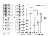
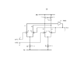
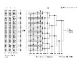
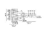
上記した本発明についてさらに詳細に説述すべく添付図面を参照して以下に説明する。図1は、本発明の一実施例のデジタルアナログ変換回路(DAC)の構成を示す図である。特に制限されないが、図1に示すデジタルアナログ変換回路は、増幅回路と組み合わせることで、液晶表示パネル等のデータ線を駆動するデータドライバに適用して好適とされる。 The above-described present invention will be described below with reference to the accompanying drawings in order to explain in more detail. FIG. 1 is a diagram showing a configuration of a digital-analog converter circuit (DAC) according to an embodiment of the present invention. Although not particularly limited, the digital-analog conversion circuit shown in FIG. 1 is preferably applied to a data driver for driving data lines such as a liquid crystal display panel by being combined with an amplifier circuit.
図1を参照すると、本実施例のデジタルアナログ変換回路においては、不図示の参照電圧発生回路から出力される第1乃至第(2×h+1)(ただし、hは所定の正整数)の参照電圧Vr1〜Vr(2×h+1)(ただし、Vr1<Vr2、・・・・<Vr(2h)<Vr(2h+1))について、(2×j−1)番目(ただし、jは1〜hの所定の正整数)のh個の参照電圧からなる第1の参照電圧グループ21と、(2×j)番目のh個の参照電圧からなる第2の参照電圧グループ22と、(2×j+1)番目のh個の参照電圧からなる第3の参照電圧グループ23とにグループ化されている。そして、参照電圧を入力デジタル信号に基づき選択するデコーダ10と、増幅回路30と、を備えている。なお、第1乃至第(2×h+1)の参照電圧Vr1〜Vr(2×h+1)は、後述される図20の参照電圧発生回路20から出力される。
Referring to FIG. 1, in the digital-analog converter circuit of this embodiment, first to (2 × h + 1) (where h is a predetermined positive integer) reference voltage output from a reference voltage generation circuit (not shown). Vr1 to Vr (2 × h + 1) (where Vr1 <Vr2,... <Vr (2h) <Vr (2h + 1)) (2 × j−1) th (where j is a predetermined number from 1 to h) A first
デコーダ10は、
(a)第1の参照電圧グループ21のh個の参照電圧Vr1、Vr3、…、Vrk、…、Vr(2h−1)を受け、入力デジタル信号の第1のビットグループ(Dn〜D(m−1))に基づき1つの参照電圧Vrkを選択する第1のサブデコーダ(本発明の第1の選択回路)111と、
(b)第2の参照電圧グループ22のh個の参照電圧Vr2、Vr4、…、Vr(k+1)、…、Vr(2h)を受け、入力デジタル信号の第1のビットグループ(Dn〜D(m−1))に基づき1つの参照電圧Vr(k+1)を選択する第2のサブデコーダ(本発明の第2の選択回路)112と、
(c)第3の参照電圧グループ23のh個の参照電圧Vr3、Vr5、…、Vr(k+2)、…、Vr(2h+1)を受け、入力デジタル信号の第1のビットグループ(Dn〜D(m−1))に基づき1つの参照電圧Vr(k+2)を選択する第3のサブデコーダ(本発明の第3の選択回路)113と、
(d)第1、第2、第3のサブデコーダ111、112、113でそれぞれ選択された参照電圧Vrk、Vr(k+1)、Vr(k+2)を受け、入力デジタル信号の第2のビットグループ(D0〜D(n−1))に基づき、重複も含めて少なくとも2個Vo1、Vo2を選択して出力する第4のサブデコーダ(本発明の第4の選択回路)13と、
を備えている。
The
(A) The h reference voltages Vr1, Vr3,..., Vrk,..., Vr (2h−1) of the first
(B) The h reference voltages Vr2, Vr4,..., Vr (k + 1),..., Vr (2h) of the second
(C) a third
(D) receives the reference voltages Vrk, Vr (k + 1), Vr (k + 2) selected by the first, second, and third sub-decoders 11 1 , 11 2 , and 11 3 , respectively, and receives the second input digital signal A fourth sub-decoder (fourth selection circuit of the present invention) 13 for selecting and outputting at least two Vo1 and Vo2 including duplication based on bit groups (D0 to D (n-1));
It has.
本実施例において、(2h+1)個の参照電圧Vr1、Vr2、Vr3、…、Vr(2h)、Vr(2h+1)に関して、第1乃至第3の参照電圧グループ21、22、23への分割において、第1、第3の参照電圧グループ21、23のj番目(j=1〜h)の参照電圧Vr(2j−1)、Vr(2j+1)は、互いに2つの参照電圧の間隔(電位差)分ずれており、第2の参照電圧グループ22のj番目の電圧V(2j)は、第1の参照電圧グループ21と第3の参照電圧グループ23のj番目の参照電圧Vr(2j−1)、Vr(2j+1)の中間の参照電圧とされる。
In the present embodiment, (2h + 1) reference voltages Vr1, Vr2, Vr3,..., Vr (2h), Vr (2h + 1) are divided into first to third
本実施例において、第1〜第3のサブデコーダ111〜113は、同一構成とされ(本明細書および添付図面では添字を省略し参照符号11で参照される場合もある)、mビットの入力デジタル信号のうち第1のビットグループDn〜D(m−1)(ただし、0<n<m−1)の値に応じて、第1〜第3の参照電圧グループ21、22、23ごとにそれぞれ1個の参照電圧を選択する。
In the present embodiment, the first to third sub-decoders 11 1 to 11 3 have the same configuration (in this specification and the accompanying drawings, the subscripts are omitted and may be referred to by reference numeral 11), and m bits. The first to third
第1のビットグループDn〜D(m−1)のビット列の値に応じて、第1のサブデコーダ111で第1の参照電圧グループ21のj番目(1≦j≦h)の参照電圧Vr(2j−1)を選択するとき、第2、第3のサブデコーダ112、113では、それぞれ、第2、第3の参照電圧グループ22、23のj番目の電圧Vr(2j)、Vr(2j+1)を選択する。ここで、k=2j−1とすると、図1に示すように、第1、第2、第3のサブデコーダ111、112、113からは、相隣る3つの参照電圧Vrk、Vr(k+1)、Vr(k+2)が選択出力される。
Depending on the value of the bit string of the first bit group Dn~D (m-1), the reference voltage Vr of the j-th first sub-decoder 11 1 in the first reference voltage group 21 (1 ≦ j ≦ h) When selecting (2j-1), the second and third sub-decoders 11 2 and 11 3 respectively select the j-th voltages Vr (2j) and Vr of the second and third
第4のサブデコーダ13は、mビットの入力デジタル信号のうち、下位ビットをなす第2のビットグループD0〜D(n−1)(D0はLSB(Least Significant Bit))のビット列の値に応じて、第1、第2、第3のサブデコーダ111、112、113でそれぞれ選択された、3個の参照電圧Vrk、Vr(k+1)、Vr(k+2)から、同一の又は相隣る2個の参照電圧Vo1、Vo2を選択し、増幅回路30のP個(ただし、Pは2以上の所定の整数)の入力端子T1・・・TP個に出力する。
The
相隣る3つの参照電圧(Vrk、Vr(k+1)、Vr(k+2))を入力する第4のサブデコーダ13では、2つの電圧(Vo1、Vo2)として、
同一参照電圧対(Vrk、Vrk)、(Vr(k+1)、Vr(k+1))、(Vr(k+2)、Vr(k+2))、
隣接参照電圧対(Vrk、Vr(k+1))、(Vr(k+1)、Vrk)、(Vrk(k+1)、Vr(k+2))、(Vrk(k+2)、Vr(k+1))
のうちのいずれか1組を選択出力する。
In the
Same reference voltage pairs (Vrk, Vrk), (Vr (k + 1), Vr (k + 1)), (Vr (k + 2), Vr (k + 2)),
Adjacent reference voltage pairs (Vrk, Vr (k + 1)), (Vr (k + 1), Vrk), (Vrk (k + 1), Vr (k + 2)), (Vrk (k + 2), Vr (k + 1))
Any one of these is selectively output.
増幅回路30は、第4のサブデコーダ13から出力された電圧Vo1、Vo2を受け、重複も含めて入力端子T1〜TPに受け、入力端子T1〜TPに入力された電圧に関して所定の演算結果(合成電圧)を出力する。本実施例では、増幅回路30は内挿アンプよりなる。
The amplifying
本実施例では、増幅回路(内挿アンプ)30には、隣接参照電圧、又は同一参照電圧がVo1、Vo2として、端子T1〜TPに入力され、隣接参照電圧間の電位差を2分割以上で内分した複数レベル(例えば後述するように4レベル)を生成することを可能としている。内挿アンプは、複数の入力端子の電圧の重み付け加算する任意の演算増幅回路で構成してもよい。 In the present embodiment, the amplifying circuit (interpolation amplifier) 30 receives adjacent reference voltages or the same reference voltage as terminals Vo1 and Vo2, and is input to terminals T1 to TP, and the potential difference between adjacent reference voltages is divided into two or more. A plurality of divided levels (for example, four levels as will be described later) can be generated. The interpolation amplifier may be configured by an arbitrary operational amplifier circuit that performs weighted addition of voltages at a plurality of input terminals.
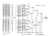
図2は、本発明の第2の実施例の構成を示す図である。図2を参照すると、本実施例は、図1の第1ビットグループDn〜D(m−1)の一部のビット信号を、プリデコーダ回路14でプリデコードしてサブデコーダ111〜113に入力する。
FIG. 2 is a diagram showing the configuration of the second exemplary embodiment of the present invention. Referring to FIG. 2, in this embodiment, a part of the bit signals of the first bit groups Dn to D (m−1) of FIG. 1 is predecoded by the
本実施例は、第1ビットグループの一部の信号をプリデコードしてサブデコーダ111〜113に入力する構成としたことにより、図1に示した実施例と比較して、サブデコーダ111〜113のスイッチトランジスタ数を削減している。なお、図2において、図1と同一構成の要素には同一の参照符号が付されている。
In this embodiment, a part of signals of the first bit group is predecoded and input to the
図2において、第1、第2、第3のサブデコーダ121、122、123は同一構成とされ(本明細書および添付図面では添字を省略し参照符号12で参照される場合もある)、第1ビットグループDn〜D(m−1)のうち所定のビットをプリデコーダ14でプリデコードした信号と、第1ビットグループDn〜D(m−1)の残りのビット信号とを入力し、それぞれ、第1、第2、第3の参照電圧グループ21、22、23のh個の参照電圧から、1個を選択する。
In FIG. 2, the first, second, and third sub-decoders 12 1 , 12 2 , and 12 3 have the same configuration (in the present specification and the accompanying drawings, the subscripts may be omitted and the
第1、第2、第3のサブデコーダ121、122、123からそれぞれ選択出力された電圧Vrk、Vr(k+1)、Vr(k+2)は第4のサブデコーダ13に入力され、前記第1の実施例と同様にして、第4のサブデコーダ13は、2つの出力信号Vo1、Vo2を重複も含めて増幅回路30の複数の入力端子T1〜TPに供給する。増幅回路30は、図1の前記第1の実施例と同様、内挿アンプからなる。
The voltages Vrk, Vr (k + 1), and Vr (k + 2) selectively output from the first, second, and third sub-decoders 12 1 , 12 2 , and 12 3 are input to the
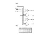
図3(A)は、図2のプリデコーダ14の構成の一例を示す図である。図3(B)は、図3(A)の回路の動作を示す真理値表である。図3のプリデコーダ14は、第1ビットグループDn〜D(m−1)の2ビットD(x+1)、Dxを入力しデコードした4ビットの信号LN1、LN2、LN3、LN4を出力する。なお、図3(A)には、Nchトランジスタで構成した場合の回路構成が示されている。なお、本明細書では、信号表記として、DxBは、Dxの反転(相補)信号を表す。
FIG. 3A shows an example of the configuration of the
図3(A)を参照すると、プリデコーダ14は、Dx(図2との対応ではDx=Dn)とその1ビット上位のD(x+1)を入力しLN1を出力する否定論理和回路NOR1と、D(x+1)とDxB(Dxの相補信号)を入力しLN2を出力するNOR2と、DxとD(x+1)Bを入力しLN3を出力するNOR3と、DxBとD(x+1)Bを入力しLN4を出力するNOR4とを備えている。(D(x+1)、Dx)=(Low、Low)、(Low、High)、(High、Low)、(High、High)に応じて、LN1、LN2、LN3、LN4がそれぞれHighとされる。プリデコーダ14でデコードされた信号LN1、LN2、LN3、LN4を受けるサブデコーダ12(Nchトランジスタ構成)では、LN1、LN2、LN3、LN4のうちHighの信号にゲートが接続するNchトランジスタスイッチがオンする。
Referring to FIG. 3A, the
図4(A)は、図2のプリデコーダ14の構成を示す図であり、Pchトランジスタで構成した場合の図である。図4(B)は、図4(A)の回路の動作を示す真理値表である。図4に示す例は、第1ビットグループDn〜D(m−1)の2ビットD(x+1)、Dxを入力しデコードした4ビットの信号LP1、LP2、LP3、LP4を出力する。
FIG. 4A is a diagram showing the configuration of the
図4(A)を参照すると、Dxの相補信号DxBと1ビット上位のD(x+1)の相補信号D(x+1)Bを入力しLP1を出力する否定論理積回路NAND1と、DxとD(x+1)Bを入力しLP2を出力するNAND2と、DxBとD(x+1)とを入力しLP3を出力するNAND3と、DxとD(x+1)を入力しLP4を出力するNOR4とを備えている。(D(x+1)、Dx)=(Low、Low)、(Low、High)、(High、Low)、(High、High)に応じて、LP1、LP2、LP3、LP4がそれぞれLowとされる。プリデコーダ14でデコードされた信号LP1、LP2、LP3、LP4を受けるサブデコーダ12(Pchトランジスタ構成)では、LP1、LP2、LP3、LP4のうちLowの信号にゲートが接続するPchトランジスタスイッチがオンする。
Referring to FIG. 4A, a NAND circuit NAND1 that inputs a complementary signal DxB of Dx and a complementary signal D (x + 1) B of D (x + 1) that is one bit higher and outputs LP1, and Dx and D (x + 1) ) NAND2 that inputs B and outputs LP2, NAND3 that inputs DxB and D (x + 1) and outputs LP3, and NOR4 that inputs Dx and D (x + 1) and outputs LP4. According to (D (x + 1), Dx) = (Low, Low), (Low, High), (High, Low), (High, High),
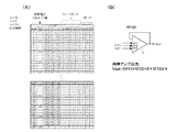
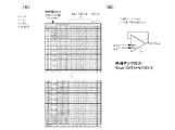
図5(A)は、図1又は図2を参照して説明した実施例に関して具体的な動作仕様の一例を表形式でまとめて示した図である。図5(B)は、図1又は図2の増幅回路(内挿アンプ)30を示している。図5に示す例は、図1又は図2において、m=8、n=2、h=64(=2^6)とし、2h+1=2*64+1=129としている。 FIG. 5A is a table collectively showing an example of specific operation specifications regarding the embodiment described with reference to FIG. 1 or FIG. FIG. 5B shows the amplifier circuit (interpolation amplifier) 30 of FIG. 1 or FIG. In the example shown in FIG. 5, m = 8, n = 2, h = 64 (= 2 ^ 6) in FIG. 1 or 2, and 2h + 1 = 2 * 64 + 1 = 129.
図5(A)において、レベル欄(0〜255)は、増幅回路(内挿アンプ)30の出力電圧レベルであり、デコーダ10への8ビットのデジタル入力信号に対応して、0〜255の256レベルが出力可能とされる。
In FIG. 5A, a level column (0 to 255) is an output voltage level of the amplifier circuit (interpolation amplifier) 30 and corresponds to an 8-bit digital input signal to the
図5(A)のVrefは、レベルと参照電圧との対応を示している。例えば図1又は図2の第1の参照電圧グループ21の1番目の参照電圧Vr1はレベル0に対応し、図1又は図2の第2の参照電圧グループ22の1番目の参照電圧Vr2はレベル2に対応し、図1又は図2の第3の参照電圧グループ23の1番目の参照電圧Vr3(第1の参照電圧グループ21の2番目の参照電圧)はレベル4に対応している。
Vref in FIG. 5A indicates the correspondence between the level and the reference voltage. For example, the first reference voltage Vr1 of the first
T1、T2は、増幅回路(内挿アンプ)30の2つの入力端子である。図5(B)を参照すると、増幅回路(内挿アンプ)30は、2つの正転入力端子T1、T2(電圧はV(T1)、V(T2))にVo1、Vo2がそれぞれ接続され、出力端が反転入力端子に接続されたボルテージフォロワ構成とされ、出力端子電圧Voutは、Vout={V(T1)+V(T2)}/2で与えられる。
図5(A)のD7−D2は、図1又は図2のD(m−1)−Dnに対応し、上位8−2=6ビット、図5(A)のD1、D0は、図1又は図2のD(n−1)−D0に対応し下位2ビットである。 D7-D2 in FIG. 5A corresponds to D (m-1) -Dn in FIG. 1 or FIG. 2, and upper 8-2 = 6 bits. D1 and D0 in FIG. Or it corresponds to D (n-1) -D0 in FIG.
図5(A)に示すように、4つの連続するレベルよりなる区間に対応して、隣接する2つの参照電圧を割当て、1つの区間の端のレベル(下位から4つ目のレベル)に対して隣の区間の最低レベルの1つの参照電圧を共有し、レベル0〜255の総数256の電圧レベルに対して、参照電圧の個数を2×h+1=2×64+1=129個でまかなっている。 As shown in FIG. 5 (A), two adjacent reference voltages are allocated corresponding to a section composed of four consecutive levels, and the end level (fourth level from the bottom) of one section is assigned. In addition, one reference voltage at the lowest level of the adjacent section is shared, and the number of reference voltages is 2 × h + 1 = 2 × 64 + 1 = 129 for a total of 256 voltage levels of levels 0 to 255.
より詳細には、図5(A)を参照すると、レベル0〜3の区間(第1区間)には、参照電圧Vr1、Vr2が割当てられ、この第1の区間の端のレベル3は、隣の第2の区間(レベル4〜7)に属する最低レベルの参照電圧Vr3と、第1の区間の参照電圧Vr2の内挿で生成される。したがって、レベル0〜3に対して、第1ビットグループ(D7−D2)に基づき、第1、第2、第3のサブデコーダ111、112、113で、参照電圧の3つ組(Vr1、Vr2、Vr3)を選択して、第4のサブデコーダ13に入力し、第4のサブデコーダ13は第2ビットグループ(D1、D0)に基づき、重複も含めて2つを選択する。
More specifically, referring to FIG. 5A, reference voltages Vr1 and Vr2 are assigned to the sections of level 0 to 3 (first section), and
より詳しくは、(D1、D0)=(0、0)のとき、第4のサブデコーダ13で(Vo1、Vo2)=(V(T1)、V(T2))=(Vr1、Vr1)を選択し、増幅回路(内挿アンプ)30は、Vout=(Vr1+Vr1)/2=Vr1を出力する。
More specifically, when (D1, D0) = (0, 0), the
(D1、D0)=(0、1)のとき、第4のサブデコーダ13で(Vo1、Vo2)=(V(T1)、V(T2))=(Vr2、Vr1)を選択し、増幅回路(内挿アンプ)30は、Vr1とVr2の中間レベルVout=(Vr2+Vr1)/2を出力する。
When (D1, D0) = (0, 1), the
(D1、D0)=(1、0)のとき、第4のサブデコーダ13で(Vo1、Vo2)=(V(T1)、V(T2))=(Vr2、Vr2)を選択し、増幅回路(内挿アンプ)30は、Vout=(Vr2+Vr2)/2=Vr2を出力する。
When (D1, D0) = (1, 0), the
(D1、D0)=(1、1)のとき、第4のサブデコーダ13で(Vo1、Vo2)=(V(T1)、V(T2))=(Vr3、Vr2)を選択し、増幅回路(内挿アンプ)30は、Vr2とVr3の中間レベルVout=(Vr3+Vr2)/2を出力する。
When (D1, D0) = (1, 1), the
同様にして、レベル4〜7の第2の区間には参照電圧Vr4、Vr5が割当てられ、この区間の端のレベル7は、隣の第3の区間(レベル8〜11)の参照電圧Vr5と、第2の区間の参照電圧Vr4の内挿で生成される。したがってレベル4〜7に対して、第1ビットグループ(D7−D2)に基づき、第1、第2、第3のサブデコーダ111、112、113で参照電圧の3つ組(Vr3、Vr4、Vr5)を選択して、第4のサブデコーダ13に入力し、第4のサブデコーダ13は、第2ビットグループ(D1、D0)に基づき、重複も含めて2つを選択する。
Similarly, reference voltages Vr4 and Vr5 are assigned to the second interval of
より詳しくは、(D1、D0)=(0、0)のとき、第4のサブデコーダ13で(Vo1、Vo2)=(V(T1)、V(T2))=(Vr3、Vr3)を選択し、増幅回路(内挿アンプ)30は、Vout=(Vr3+Vr3)/2=Vr3を出力する。
More specifically, when (D1, D0) = (0, 0), the
(D1、D0)=(0、1)のとき、第4のサブデコーダ13で(Vo1、Vo2)=(V(T1)、V(T2))=(Vr4、Vr3)を選択し、増幅回路(内挿アンプ)30は、Vr3とVr4の中間レベルVout=(Vr4+Vr3)/2を出力する。
When (D1, D0) = (0, 1), the
(D1、D0)=(1、0)のとき、第4のサブデコーダ13で(Vo1、Vo2)=(V(T1)、V(T2))=(Vr4、Vr4)を選択し、増幅回路(内挿アンプ)30は、Vout=(Vr4+Vr4)/2=Vr4を出力する。
When (D1, D0) = (1, 0), the
(D1、D0)=(1、1)のとき、第4のサブデコーダ13で(Vo1、Vo2)=(V(T1)、V(T2))=(Vr5、Vr4)を選択し、増幅回路(内挿アンプ)30は、Vr4とVr5の中間レベルVout=(Vr5+Vr4)/2を出力する。
When (D1, D0) = (1, 1), the
レベル252〜255の第64の区間には、参照電圧Vr127、Vr128が割当てられ、この区間の端のレベル255は、隣の参照電圧Vr129(Vr129は、h=64の場合の最上位の参照電圧Vr(2h+1)=Vr(2×64+1)である)と、第64の区間内の参照電圧Vr128の内挿で生成される。したがって、レベル252〜255に対して、第1ビットグループ(D7−D2)に基づき、第1、第2、第3のサブデコーダ111、112、113で、参照電圧の3つ組(Vr127、Vr128、Vr129)を選択して、第4のサブデコーダ13に入力し、第4のサブデコーダ13は第2ビットグループ(D1、D0)に基づき、重複も含めて2つを選択する。
Reference voltages Vr127 and Vr128 are assigned to the 64th section of levels 252 to 255, and level 255 at the end of this section is an adjacent reference voltage Vr129 (Vr129 is the highest reference voltage when h = 64). Vr (2h + 1) = Vr (2 × 64 + 1)) and the reference voltage Vr128 in the 64th section is generated by interpolation. Therefore, for levels 252 to 255, based on the first bit group (D7-D2), the first, second, and third sub-decoders 11 1 , 11 2 , and 11 3 have a reference voltage triplet ( Vr127, Vr128, and Vr129) are selected and input to the
より詳しくは、(D1、D0)=(0、0)のとき、第4のサブデコーダ13で(Vo1、Vo2)=(V(T1)、V(T2))=(Vr127、Vr127)を選択し、増幅回路(内挿アンプ)30は、Vout=(Vr127+Vr127)/2=Vr127を出力する。
More specifically, when (D1, D0) = (0, 0), the
(D1、D0)=(0、1)のとき、第4のサブデコーダ13で(Vo1、Vo2)=(V(T1)、V(T2))=(Vr128、Vr127)を選択し、増幅回路(内挿アンプ)30は、Vr127とVr128の中間レベルVout=(Vr128+Vr127)/2を出力する。
When (D1, D0) = (0, 1), the
(D1、D0)=(1、0)のとき、第4のサブデコーダ13で(Vo1、Vo2)=(V(T1)、V(T2))=(Vr128、Vr128)を選択し、増幅回路(内挿アンプ)30は、Vout=(Vr128+Vr128)/2=Vr128を出力する。
When (D1, D0) = (1, 0), the
(D1、D0)=(1、1)のとき、第4のサブデコーダ13で(Vo1、Vo2)=(V(T1)、V(T2))=(Vr129、Vr128)を選択し、増幅回路(内挿アンプ)30は、Vr128とVr129の中間レベルVout=(Vr129+Vr128)/2を出力する。
When (D1, D0) = (1, 1), the
図6は、図5に示した実施例(m=8、n=2、h=64)において、図1の第1、第2、第3のサブデコーダ111、112、113の構成の一例を示す図である。なお、前述したように、第1、第2、第3のサブデコーダ111、112、113は同一構成とされる。図6では、図1の第1ビットグループDn〜D(m−1)を6ビット(D2、D2B、・・・D7、D7B)として、参照電圧を下位ビット(D2、D2B)側から上位ビット(D7、D7B)へ向かって順次選択する。 FIG. 6 shows the configuration of the first, second, and third sub-decoders 11 1 , 11 2 , 11 3 of FIG. 1 in the embodiment (m = 8, n = 2, h = 64) shown in FIG. It is a figure which shows an example. As described above, the first, second, and third sub-decoders 11 1 , 11 2 , and 11 3 have the same configuration. In FIG. 6, the first bit group Dn to D (m−1) in FIG. 1 is set to 6 bits (D2, D2B,... D7, D7B), and the reference voltage is set to the upper bits from the lower bit (D2, D2B) side. Selects sequentially toward (D7, D7B).
図6では、図面の都合上、3つの参照電圧を1組としてh個の参照電圧が1つのサブデコーダ回路に入力される構成として示されているが、
第1の参照電圧グループ21(Vr1、Vr3、…、Vrk、・・・、Vr125、Vr127)、第2の参照電圧グループ22(Vr2、Vr4、…、Vr(k+1)、…、Vr126、Vr128)、第3の参照電圧グループ23(Vr3、Vr5、…、Vr(k+2)、…、Vr127、Vr129)に対応して図6のサブデコーダ11を3つ備え、第1乃至第3のサブデコーダ111〜113から、Vrk、Vr(k+1)、Vr(k+2)がそれぞれ出力される。
In FIG. 6, for the convenience of the drawing, three reference voltages are shown as a set and h reference voltages are input to one sub-decoder circuit.
First reference voltage group 21 (Vr1, Vr3,..., Vrk,..., Vr125, Vr127), second reference voltage group 22 (Vr2, Vr4,..., Vr (k + 1),..., Vr126, Vr128) Corresponding to the third reference voltage group 23 (Vr3, Vr5,..., Vr (k + 2),..., Vr127, Vr129), three
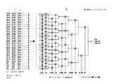
第1のサブデコーダ111は、トーナメント構成とされ、第1ビットグループの下位ビット(D2、D2B)にそれぞれ接続するNchトランジスタスイッチにより、第1の参照電圧グループ21の隣接する2つの参照電圧(Vr1、Vr3)、(Vr5、Vr7)、・・・(Vr125、Vr127)の一方を選択し、(D3、D3B)にそれぞれ接続するNchトランジスタスイッチでは、1ビット下位の(D2、D2B)にそれぞれ接続するNchトランジスタスイッチで選択された2つの参照電圧の一方を選択し、以下、上位のビットに接続するNchトランジスタスイッチでは、1ビット下位で選択された2つの参照電圧の一方を選択し、(D7、D7B)に接続するNchトランジスタスイッチでは、1つ下位のビット(D6、D6B)に接続するNchトランジスタスイッチで選択された2つの参照電圧の一方の参照電圧Vrkを出力する。第2、第3のサブデコーダ112、113も同様にして、第1ビットグループ(D2、D2B、・・・、D7、D7B)に基づき、第2、第3の参照電圧グループ22、23から1つの参照電圧Vr(k+1)、Vr(k+2)をそれぞれ出力する。なお、例えばD2に接続するNchトランジスタスイッチは、D2がゲートに接続され、D2がHighのときオンし、Lowのときオフする。D2Bに接続するNchトランジスタスイッチは、D2Bがゲートに接続され、D2BがLowのときオンし、Highのときオフする。
The
図6に示したサブデコーダ11のトランジスタスイッチの総数は126個である。また、図6に示したサブデコーダ11においては、第1ビットグループの下位ビット(例えばD2、D2B)に接続するNchトランジスタスイッチは電圧レベルの近い参照電圧を選択する構成とされている。かかる構成により、Nchトランジスタスイッチの一部は大きなドレイン耐圧(ドレイン−基板間の耐圧)を要しない。したがって耐圧に応じて、トランジスタスイッチサイズを小さくして、回路面積を削減することも可能である。 The total number of transistor switches in the sub-decoder 11 shown in FIG. Further, in the sub-decoder 11 shown in FIG. 6, the Nch transistor switch connected to the lower bits (for example, D2 and D2B) of the first bit group is configured to select a reference voltage having a close voltage level. With this configuration, a part of the Nch transistor switch does not require a large drain breakdown voltage (drain-substrate breakdown voltage). Therefore, the circuit area can be reduced by reducing the transistor switch size in accordance with the breakdown voltage.
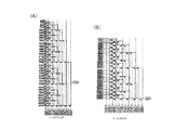
図7は、図5に示した実施例(m=8、n=2、h=64)において、図2の第1、第2、第3のサブデコーダ121、122、123の構成を示す図である(第1、第2、第3のサブデコーダ121、122、123は同一構成である)。 7 shows the configuration of the first, second, and third sub-decoders 12 1 , 12 2 , and 12 3 of FIG. 2 in the embodiment (m = 8, n = 2, h = 64) shown in FIG. (The first, second, and third sub-decoders 12 1 , 12 2 , and 12 3 have the same configuration).
図2の第1ビットグループ(D2、D2B、・・・D7、D7B)のうち、下位2ビット(D2、D2B、D3、D3B)は、プリデコーダ14に入力され(図3の(Dx、DxB、D(x+1)、D(x+1)B)、参照電圧を、プリデコーダ14の出力信号LN1〜LN4を用いて選択し、LN1〜LN4で選択された16個の参照電圧を、第1ビットグループの上位ビット(D5、D5B)、(D6、D6B)、(D7、D7B)を用いてトーナメント方式で(D5、D5B)から(D7、D7B)に向かって順次選択する。
Of the first bit group (D2, D2B,... D7, D7B) in FIG. 2, the lower 2 bits (D2, D2B, D3, D3B) are input to the predecoder 14 ((Dx, DxB in FIG. 3). , D (x + 1), D (x + 1) B), reference voltages are selected using the output signals LN1 to LN4 of the
なお、図7では、図面作成の都合で、3つの参照電圧を1組としてh個の参照電圧がサブデコーダ12に入力される構成として示されているが、第1の参照電圧グループ21(Vr1、Vr3、…、Vrk、・・・、Vr125、Vr127)、第2の参照電圧グループ22(Vr2、Vr4、…、Vr(k+1)、…、Vr126、Vr128)、第3の参照電圧グループ23(Vr3、Vr5、…、Vr(k+2)、…、Vr127、Vr129)に対応して図7のサブデコーダ12を3つ備え、第1乃至第3のサブデコーダ121〜123のそれぞれからVrk、Vr(k+1)、Vr(k+2)が出力される。
In FIG. 7, for convenience of drawing, a configuration in which h reference voltages are input to the sub-decoder 12 with three reference voltages as one set is shown. However, the first reference voltage group 21 (Vr1 , Vr3, ..., Vrk, ..., Vr125, Vr127), the second reference voltage group 22 (Vr2, Vr4, ..., Vr (k + 1), ..., Vr126, Vr128), the third reference voltage group 23 ( .., Vr127, Vr129) corresponding to Vr3, Vr5,..., Vr (k + 2),..., Vr127, Vr129), and the three
第1ビットグループ(D2、D2B、・・・D7、D7B)の下位2ビット(D2、D2B、D3、D3B)に基づき、図2のプリデコーダ14の出力LN1、LN2、LN3、LN4はいずれか1つがHighとなり、第1のサブデコーダ121では、第1の参照電圧グループ21の連続する4つ参照電圧(Vr1、Vr3、Vr5、Vr7)、(Vr9、Vr11、Vr13、Vr15)、・・・(Vr121、Vr123、Vr125、Vr127)の一つを選択する。
Based on the lower 2 bits (D2, D2B, D3, D3B) of the first bit group (D2, D2B,... D7, D7B), any of the outputs LN1, LN2, LN3, LN4 of the
(D4、D4B)にそれぞれ接続するNchトランジスタスイッチでは、LN1、LN2、LN3、LN4にそれぞれ接続するNchトランジスタスイッチで選択された、2つの隣接する4つ組の参照電圧の各1つ(例えば、参照電圧(Vr1、Vr3、Vr5、Vr7)のうちの選択された1つと、参照電圧(Vr9、Vr11、Vr13、Vr15)のうちの選択された1つ)の一方を選択する。 In each of the Nch transistor switches connected to (D4, D4B), each one of two adjacent quadruple reference voltages selected by the Nch transistor switches respectively connected to LN1, LN2, LN3, and LN4 (for example, One of the selected ones of the reference voltages (Vr1, Vr3, Vr5, Vr7) and the selected one of the reference voltages (Vr9, Vr11, Vr13, Vr15) is selected.
(D5、D5B)にそれぞれ接続するNchトランジスタスイッチでは、(D4、D4B)にそれぞれ接続するNchトランジスタスイッチで選択された2つの参照電圧の一方を選択し、(D6、D6B)にそれぞれ接続するNchトランジスタスイッチでは、(D5、D5B)にそれぞれ接続するNchトランジスタスイッチで選択された2つの参照電圧の一方を選択し、(D7、D7B)にそれぞれ接続するNchトランジスタスイッチでは、(D6、D6B)にそれぞれ接続するNchトランジスタスイッチで選択された2つの参照電圧の一方の参照電圧Vrkを出力する。第2、第3のサブデコーダ122、123も同様にして、第1ビットグループ(D2、D2B、・・・、D7、D7B)に基づき、第2、第3の参照電圧グループ22、23から1つの参照電圧Vr(k+1)、Vr(k+2)をそれぞれ出力する。図7に示したサブデコーダ12のトランジスタ総数は94個である。また、図7に示したサブデコーダ12においても、第1ビットグループの下位ビットに接続されるNchトランジスタスイッチの一部は大きなドレイン耐圧(ドレイン−基板間の耐圧)を用いることを要しなくしている。したがって耐圧に応じて、トランジスタスイッチサイズを小さくして、回路面積を削減することも可能である。
In the Nch transistor switches connected to (D5, D5B), one of the two reference voltages selected by the Nch transistor switches connected to (D4, D4B) is selected, and the Nch connected to (D6, D6B), respectively. the transistor switches, (D5,
図8は、図5に示した実施例(m=8、n=2、h=64)において、図1又は図2の第4のサブデコーダ13の構成を示す図である。図8において、Vrk、Vr(k+1)、Vr(k+2)は、第1乃至第3のサブデコーダ111〜113(121〜123)で選択され第4のサブデコーダ13に入力される参照電圧である。V(T1)、V(T2)は増幅回路30の入力端子T1、T2の電圧である。
FIG. 8 is a diagram showing a configuration of the
図8を参照すると、V(T1)は、D1Bに接続するNchトランジスタスイッチと、D0Bに接続するNchトランジスタスイッチを介してVrkに接続され、D1Bに接続するNchトランジスタスイッチと、D0に接続するNchトランジスタスイッチを介してVr(k+1)に接続されており、さらにV(T1)は、D1に接続するNchトランジスタスイッチと、D0Bに接続するNchトランジスタスイッチを介してVr(k+1)に接続され、D1に接続するNchトランジスタスイッチと、D0に接続するNchトランジスタスイッチを介してVr(k+2)に接続されている。V(T2)は、D1に接続するNchトランジスタスイッチを介してVr(k+1)に接続され、D1Bに接続するNchトランジスタスイッチを介してVrkに接続されている。 Referring to FIG. 8, V (T1) is connected to Vrk via an Nch transistor switch connected to D1B, an Nch transistor switch connected to D0B, connected to D1B, and Nch connected to D0. Vr (k + 1) is connected to Vr (k + 1) via a transistor switch, and V (T1) is further connected to Vr (k + 1) via an Nch transistor switch connected to D1 and an Nch transistor switch connected to D0B. Is connected to Vr (k + 2) via an Nch transistor switch connected to D0 and an Nch transistor switch connected to D0. V (T2) is connected to Vr (k + 1) via an Nch transistor switch connected to D1, and is connected to Vrk via an Nch transistor switch connected to D1B.
かかる構成の第4のサブデコーダ13において、
(D1、D0)=(0、0)のとき、(V(T1)、V(T2))=(Vrk、Vrk)が出力される。
In the
When (D1, D0) = (0, 0), (V (T1), V (T2)) = (Vrk, Vrk) is output.
(D1、D0)=(0、1)のとき、(V(T1)、V(T2))=(Vr(k+1)、Vrk)が出力される。 When (D1, D0) = (0, 1), (V (T1), V (T2)) = (Vr (k + 1), Vrk) is output.
(D1、D0)=(1、0)のとき、(V(T1)、V(T2))=(Vr(k+1)、Vr(k+1))が出力される。 When (D1, D0) = (1, 0), (V (T1), V (T2)) = (Vr (k + 1), Vr (k + 1)) is output.
(D1、D0)=(1、1)のとき、(V(T1)、V(T2))=(Vr(k+2)、Vr(k+1))が出力される。 When (D1, D0) = (1, 1), (V (T1), V (T2)) = (Vr (k + 2), Vr (k + 1)) is output.
図9は、図5に示した実施例における図2の回路12の構成を示す図であり、図7のNchトランジスタをPchトランジスタで構成したものである。図9に示すように、(D2、D2B、D3、D3B)に基づきプリデコーダ14(図4の(Dx、DxB、D(x+1)、D(x+1)B)の出力LP1、LP2、LP3、LP4はいずれか1つがHighとなり、サブデコーダ121では、連続する4つ参照電圧(Vr1、Vr3、Vr5、Vr7)、(Vr9、Vr11、Vr13、Vr15)、・・・(Vr121、Vr123、Vr125、Vr127)の一つを選択する。(D4、D4B)に接続するNchトランジスタスイッチでは、LP1、LP2、LP3、LP4で選択された、2つの隣接する4つ組の参照電圧の各1つ(例えば、参照電圧(Vr1、Vr3、Vr5、Vr7)のうちの選択された1つと、参照電圧(Vr9、Vr11、Vr13、Vr15)のうちの選択された1つ)の一方を選択する。(D5、D5B)に接続するPchトランジスタスイッチでは、(D4、D4B)に接続するPchトランジスタスイッチによって選択された2つの参照電圧の一方を選択し、(D6、D6B)に接続するPchトランジスタスイッチでは、(D5、D5B)に接続するPchトランジスタスイッチで選択された2つの参照電圧の一方を選択し、(D7、D7B)に接続するPchトランジスタスイッチでは、(D6、D6B)に接続するPchトランジスタスイッチで選択された2つの参照電圧の一方の参照電圧Vrkを選択し出力する。第2、第3のサブデコーダ122、123も同様にして、第1ビットグループ(D2、D2B、・・・、D7、D7B)に基づき、第2、第3の参照電圧グループ22、23から1つの参照電圧Vr(k+1)、Vr(k+2)をそれぞれ出力する。この場合、サブデコーダ12のPchトランジスタスイッチの総数は94個である。
FIG. 9 is a diagram showing a configuration of the
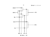
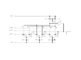
図10は、図5(B)の増幅回路(内挿アンプ)30の構成を示す図である(なお同様な構成が特許文献2の図5に開示されている)。図10に示すように、共通接続されたソースが電流源113に接続され、ゲートが端子T1(電圧V(T1))と出力端子3(出力端子電圧Vout)にそれぞれ接続されたNchトランジスタ101、102よりなる第1の差動対と、共通接続されたソースが電流源114に接続されゲートが端子T2(電圧V(T2))と出力端子3にそれぞれ接続されたNchトランジスタ103、104よりなる第2の差動対と、Nchトランジスタ101、103の共通接続されたドレインと電源VDD間に接続されたPchトランジスタ111と、Nchトランジスタ102、104の共通接続されたドレインと電源VDD間に接続され、ゲートとドレインが接続されるとともに、ゲートがPchトランジスタ111のゲートに接続されたPchトランジスタ112と、Pchトランジスタ111のドレインとNchトランジスタ101、103の共通接続されたドレインとの接続点が入力端に接続され、出力端が出力端子3に接続された増幅段109と、を備えている。Pchトランジスタ111、112はカレントミラーを構成している。Nchトランジスタ101、102、103、104は同一サイズとされ、電流源113、114の電流値が等しい。Nchトランジスタ101、102、103、104のドレイン電流はID1、ID2、ID3、ID4は以下で与えられる。
FIG. 10 is a diagram illustrating a configuration of the amplifier circuit (interpolation amplifier) 30 in FIG. 5B (a similar configuration is disclosed in FIG. 5 of Patent Document 2). As shown in FIG. 10 , an
ID1=(β/2)(V(T1)−VTH))^2 ・・・(1)
ID2=(β/2)(Vout−VTH))^2 ・・・(2)
ID3=(β/2)(V(T2)−VTH))^2 ・・・(3)
ID4=(β/2)(Vout−VTH))^2 ・・・(4)
ID1 = (β / 2) (V (T1) −VTH)) ^ 2 (1)
ID2 = (β / 2) (Vout−VTH)) ^ 2 (2)
ID3 = (β / 2) (V (T2) −VTH)) ^ 2 (3)
ID4 = (β / 2) (Vout−VTH)) ^ 2 (4)
ただし、βは利得係数であり、β(=μ(W/L)(εx/tox)、ただしμは電子の実効移動度、εxはゲート絶縁膜の誘電率、toxはゲート絶縁膜の膜厚、Wはチャネル幅、Lはチャネル長)、VTHは閾値電圧である。 Where β is a gain coefficient, β (= μ (W / L) (εx / tox), where μ is the effective mobility of electrons, εx is the dielectric constant of the gate insulating film, and tox is the film thickness of the gate insulating film. , W is the channel width, L is the channel length), and VTH is the threshold voltage.
電流ID2+ID4はカレントミラーの入力側のPchトランジスタ112に流れる電流(入力電流)であり、電流ID1+ID3はカレントミラー回路の出力側のPchトランジスタ111に流れる電流(出力電流)であり、カレントミラー回路の入力電流が出力電流に等しくなるように制御される。
The current ID2 + ID4 is a current (input current) flowing through the Pch transistor 112 on the input side of the current mirror, and the current ID1 + ID3 is a current (output current) flowing through the
ID1+ID3=ID2+ID4 ・・・(5) ID1 + ID3 = ID2 + ID4 (5)
式(1)乃至(4)の括弧内を展開して式(5)に代入し、VTHの一次項に関して両辺を等しいとして、V(T1)+V(T2)=2×Vout、すなわち、
Vout={V(T1)+V(T2)}/2 ・・・(6)
となる。あるいは、第1、第2の差動対の相互コンダクタンスをgmとして、ID1−ID2=gm(V(T1)−Vout)、ID3−ID4=gm(V(T2)−Vout)を式(5)に代入することで式(6)が導かれる。
Expanding the parentheses in Equations (1) to (4) and substituting them into Equation (5), assuming that both sides are equal with respect to the primary term of VTH, V (T1) + V (T2) = 2 × Vout, that is,
Vout = {V (T1) + V (T2)} / 2 (6)
It becomes. Alternatively, ID1-ID2 = gm (V (T1) -Vout) and ID3-ID4 = gm (V (T2) -Vout) are expressed by Equation (5) where gm is the mutual conductance of the first and second differential pairs. (6) is derived by substituting into.
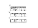
図11は、DACのスイッチの数を本実施例と比較してまとめたものである。図23、図24の構成の場合、図11(A)に示すように、8ビットでは、1stデコーダのトーナメント1、トーナメント2、トーナメント3は、126、126、62となり、2ndデコーダは12となり計326個となる。10ビットでは、1stデコーダのトーナメント1、トーナメント2、トーナメント3は、510、510、254となり、2ndデコーダは12となり計1286個となる。
FIG. 11 summarizes the number of DAC switches in comparison with the present embodiment. In the case of the configuration of FIGS. 23 and 24, as shown in FIG. 11 (A), in 8 bits,
図5の実施例において、図1、図6、図8の構成の場合、図11(B)に示すように、8ビットでは、回路11は、126、回路13は8個であり、126×3+8=386個となる。10ビットでは、回路11は510、回路13は8個であり、510×3+8=1538個となる。
In the embodiment of FIG. 5, in the case of the configuration of FIGS. 1, 6, and 8, as shown in FIG. 11B, in 8 bits, there are 126
図5の実施例において、プリデコーダを備えた図2、図7、図8の構成の場合、図11(C)に示すように、8ビットでは、回路11は、94、回路13は8個であり、94×3+8=290個となる。10ビットでは、回路11は382、回路13は8個であり、382×3+8=1154個となる。
In the embodiment of FIG. 5, in the case of the configuration of FIG. 2, FIG. 7 and FIG. 8 with predecoders, as shown in FIG. 11C, in 8 bits, 94
図1の実施例の場合、特許文献1と較べてトランジスタスイッチ素子数は増加するが、プリコデーダを備えた図2の実施例では、トランジスタスイッチ素子数は削減され、省面積が実現できる。
In the embodiment of FIG. 1, the number of transistor switch elements is increased as compared with
また、図6の構成の場合、m=8、n=2に対して、第1のサブデコーダ111、図8の第4のサブデコーダ13において、第1の参照電圧グループ21からVrkとして選択出力され、V(T1)/V(T2)として選択されるパスに直列に挿入されるトランジスタスイッチの総数は最大8個である。同様にして第2のサブデコーダ112、第4のサブデコーダ13において、第2の参照電圧グループ22からVr(k+1)として選択出力され、V(T1)/V(T2)として選択されるパスに直列に挿入されるスイッチの数は最大8個である。同様にして第3のサブデコーダ113、第4のサブデコーダ13において、第3の参照電圧グループ23からVr(k+2)として選択出力され、V(T1)/V(T2)として選択されるパスに直列に挿入されるトランジスタスイッチの個数は、最大8個である。
In the case of the configuration of FIG. 6, for m = 8 and n = 2, the
また、図7の構成の場合、m=8、n=2に対して、第1のサブデコーダ121、図8の第4のサブデコーダ13において、第1の参照電圧グループ21からVrkとして選択出力され、V(T1)/V(T2)として選択されるパスに直列に挿入されるスイッチの数は最大7個である。同様にして、第2のサブデコーダ122、第4のサブデコーダ13において、第2の参照電圧グループ22からVr(k+1)として選択出力され、V(T1)/V(T2)として選択されるパスに直列に挿入されるスイッチの数は最大7個である。第3のサブデコーダ123、第4のサブデコーダ13において、第3の参照電圧グループ23からVr(k+2)として選択出力され、V(T1)/V(T2)として選択されるパスに直列に挿入されるトランジスタスイッチの個数は最大7個である。
In the case of the configuration of FIG. 7, for m = 8 and n = 2, the
図12(A)は、図1又は図2に示した実施例について図5とは異なる動作仕様を説明する図である。本実施例は、図1において、m=8、n=3、h=32(2h+1=65、したがって参照電圧はVr1〜V65)とした場合である。図12(B)は、図1、図2の増幅回路(内挿アンプ)30の構成を示している。 FIG. 12A is a diagram for explaining operation specifications different from those in FIG. 5 in the embodiment shown in FIG. 1 or FIG. In this embodiment, in FIG. 1, m = 8, n = 3, h = 32 (2h + 1 = 65, and therefore the reference voltages are Vr1 to V65). FIG. 12B shows the configuration of the amplifier circuit (interpolation amplifier) 30 shown in FIGS.
図12(A)のレベル(0〜255)は、増幅回路(内挿アンプ)30の出力電圧レベルであり、0〜255の256レベルが出力可能とされる。 The level (0 to 255) in FIG. 12A is the output voltage level of the amplifier circuit (interpolation amplifier) 30, and 256 levels from 0 to 255 can be output.
図12(A)のVrefは、レベル(増幅回路(内挿アンプ)30の出力電圧レベル)と参照電圧との対応を示している。例えば第1の参照電圧グループ21の1番目の参照電圧Vr1はレベル0に対応し、第2の参照電圧グループ22の1番目の参照電圧Vr2はレベル4に対応し、第3の参照電圧グループ23の1番目の参照電圧Vr3(第1の参照電圧グループ21の2番目の参照電圧)はレベル8に対応している。
Vref in FIG. 12A indicates the correspondence between the level (the output voltage level of the amplifier circuit (interpolation amplifier) 30) and the reference voltage. For example, the first reference voltage Vr1 of the first
図12(A)のT1、T2、T3は、増幅回路30の入力端子である。
T1, T2, and T3 in FIG. 12A are input terminals of the
図12(A)のD7−D3は、図1又は図2のD(m−1)−Dn、すなわち上位8−3=5ビット、D2−D0は、図1又は図2のD(n−1)−D0、すなわち下位3ビットである。 D7-D3 in FIG. 12A is D (m-1) -Dn in FIG. 1 or FIG. 2, that is, upper 8-3 = 5 bits, and D2-D0 is D (n− in FIG. 1 or FIG. 1) -D0, ie the lower 3 bits.
図1又は図2の第4のサブデコーダ13は、Vo1、Vo2を増幅回路(内挿アンプ)30の3つの端子T1、T2、T3に出力する。増幅回路(内挿アンプ)30は、3つの端子T1、T2、T3の電圧をV(T1)、V(T2)、V(T3)として、(V(T1)+V(T2)+2×V(T3))/4の電圧を出力する。 The fourth sub-decoder 13 shown in FIG. 1 or 2 outputs Vo1 and Vo2 to the three terminals T1, T2, and T3 of the amplifier circuit (interpolation amplifier) 30. The amplifying circuit (interpolation amplifier) 30 has (V (T1) + V (T2) + 2 × V ( T3)) / 4 voltage is output.
図12(A)に示す例では、8つの連続するレベルよりなる区間に対応して、連続する2つの参照電圧を割当て、1つの区間の端のレベル(8つ目のレベル)に対して隣の区間の1つの参照電圧を共有し、0〜255の256のレベルに対して参照電圧を、1/4の64+1=65としている。 In the example shown in FIG. 12A, two consecutive reference voltages are allocated corresponding to a section composed of eight consecutive levels, and adjacent to the end level (eighth level) of one section. One reference voltage in the interval is shared, and the reference voltage is set to 1/4 of 64 + 1 = 65 with respect to 256 levels of 0 to 255.
レベル0〜7の第1の区間には、参照電圧Vr1、Vr2が割当てられ、第1の区間の上側の3つのレベル5、6、7では、第2の区間(レベル8〜15)の参照電圧Vr3と、第1の区間の参照電圧Vr2の内挿で生成される。したがって、レベル0〜7に対して、第1ビットグループ(D7−D3)に基づき、第1、第2、第3のサブデコーダ111、112、113で、3つの連続ステップの参照電圧(Vr1、Vr2、Vr3)を選択して、第4のサブデコーダ13に入力し、第4のサブデコーダ13は、第2ビットグループ(D2、D1、D0)に基づき、2つの電圧Vo1、Vo2(Vo1、Vo2が同一電圧も含む)を選択し、Vo1、Vo2を重複も含めて、増幅回路30の3つの入力端子T1、T2、T3に出力する。
Reference voltages Vr1 and Vr2 are assigned to the first section of levels 0 to 7, and in the three
より詳しくは、(D2、D1、D0)=(0、0、0)のとき、第4のサブデコーダ13で(V(T1)、V(T2)、V(T3))=(Vr1、Vr1、Vr1)を選択し、増幅回路(内挿アンプ)30は、Vout=(Vr1+Vr1+2×Vr1)/4=Vr1を出力する。 More specifically, when (D2, D1, D0) = (0, 0, 0), the fourth sub-decoder 13 uses (V (T1), V (T2), V (T3)) = (Vr1, Vr1). , Vr1) and the amplifier circuit (interpolation amplifier) 30 outputs Vout = (Vr1 + Vr1 + 2 × Vr1) / 4 = Vr1.
(D2、D1、D0)=(0、0、1)のとき、第4のサブデコーダ13で、(V(T1)、V(T2)、V(T3))=(Vr2、Vr1、Vr1)を選択し、増幅回路(内挿アンプ)30は、Vout=(Vr2+Vr1+2×Vr1)/4=Vr1+(Vr2−Vr1)/4を出力する。
When (D2, D1, D0) = (0, 0, 1), in the
(D2、D1、D0)=(0、1、0)で第4のサブデコーダ13で、(V(T1)、V(T2)、V(T3))=(Vr1、Vr1、Vr2)を選択し、増幅回路(内挿アンプ)30は、Vout=(Vr1+Vr1+2×Vr2)/4=Vr1+(Vr2−Vr1)/2を出力する。
(D2, D1, D0) = (0, 1, 0) and the
(D2、D1、D0)=(0、1、1)で第4のサブデコーダ13で、(V(T1)、V(T2)、V(T3))=(Vr2、Vr1、Vr2)を選択し、増幅回路(内挿アンプ)30は、Vout=(Vr2+Vr1+2×Vr2)/4=Vr1+(Vr2−Vr1)×3/4を出力する。
(D2, D1, D0) = (0, 1, 1) and the
(D2、D1、D0)=(1、0、0)で第4のサブデコーダ13で、(V(T1)、V(T2)、V(T3))=(Vr2、Vr2、Vr2)を選択し、増幅回路(内挿アンプ)30は、Vout=(Vr2+Vr2+2×Vr2)/4=Vr2を出力する。
(D2, D1, D0) = (1, 0, 0) and the
(D2、D1、D0)=(1、0、1)で第4のサブデコーダ13で(V(T1)、V(T2)、V(T3))=(Vr3、Vr2、Vr2)を選択し、増幅回路(内挿アンプ)30は、Vout=(Vr3+Vr2+2×Vr2)/4=Vr2+(Vr3−Vr2)/4を出力する。
When (D2, D1, D0) = (1, 0, 1), the
(D2、D1、D0)=(1、1、0)で第4のサブデコーダ13で、(V(T1)、V(T2)、V(T3))=(Vr2、Vr2、Vr3)を選択し、増幅回路(内挿アンプ)30は、Vout=(Vr2+Vr2+2×Vr3)/4=Vr2+(Vr3−Vr2)/2を出力する。
(D2, D1, D0) = (1, 1, 0) and the
(D2、D1、D0)=(1、1、1)で第4のサブデコーダ13で、(V(T1)、V(T2)、V(T3))=(Vr3、Vr2、Vr3)を選択し、増幅回路(内挿アンプ)30は、Vout=(Vr3+Vr2+2×Vr3)/4=Vr2+(Vr3−Vr2)×3/4を出力する。
(D2, D1, D0) = (1, 1, 1) and the
レベル248〜255の第32区間には参照電圧Vr63、Vr64が割当てられ、第32区間の上側の3つのレベル253、254、255では、電圧Vr65と、第32区間の参照電圧Vr64の内挿で生成される。
Reference voltages Vr63 and Vr64 are assigned to the 32nd section of levels 248 to 255, and the three
第1ビットグループ(D7−D3)に基づき、第1、第2、第3のサブデコーダ111、112、113で、3つの連続ステップの参照電圧(Vr63、Vr64、Vr65)を選択して、第4のサブデコーダ13に入力し、第4のサブデコーダ13は第2ビットグループ(D2、D1、D0)に基づき、2つの電圧Vo1、Vo2(Vo1、Vo2が同一電圧も含む)を選択し、Vo1、Vo2を重複も含めて、増幅回路30の3つの入力端子T1、T2、T3に出力する。
Based on the first bit group (D7-D3), the first, second, and third sub-decoders 11 1 , 11 2 , and 11 3 select the reference voltages (Vr63, Vr64, and Vr65) of three consecutive steps. The
より詳しくは、(D2、D1、D0)=(0、0、0)のとき、第4のサブデコーダ13で、(V(T1)、V(T2)、V(T3))=(Vr63、Vr63、Vr63)を選択し、増幅回路(内挿アンプ)30は、Vout=(Vr63+Vr63+2×Vr63)/4=Vr63を出力する。
More specifically, when (D2, D1, D0) = (0, 0, 0), the
(D2、D1、D0)=(0、0、1)のとき、第4のサブデコーダ13で、(V(T1)、V(T2)、V(T3))=(Vr64、Vr63、Vr63)を選択し、増幅回路(内挿アンプ)30は、Vout=(Vr64+Vr63+2×Vr63)/4=Vr63+(Vr64−Vr63)/4を出力する。
When (D2, D1, D0) = (0, 0, 1), in the
(D2、D1、D0)=(0、1、0)のとき、第4のサブデコーダ13で、(V(T1)、V(T2)、V(T3))=(Vr63、Vr63、Vr64)を選択し、増幅回路(内挿アンプ)30は、Vout=(Vr63+Vr63+2×Vr64)/4=Vr63+(Vr64−Vr63)/2を出力する。
When (D2, D1, D0) = (0, 1, 0), in the
(D2、D1、D0)=(0、1、1)のとき、第4のサブデコーダ13で、(V(T1)、V(T2)、V(T3))=(Vr64、Vr63、Vr64)を選択し、増幅回路(内挿アンプ)30は、Vout=(Vr64+Vr63+2×Vr64)/4=Vr63+(Vr64−Vr63)×3/4を出力する。
When (D2, D1, D0) = (0, 1, 1), in the
(D2、D1、D0)=(1、0、0)のとき、第4のサブデコーダ13で、(V(T1)、V(T2)、V(T3))=(Vr64、Vr64、Vr64)を選択し、増幅回路(内挿アンプ)30は、Vout=(Vr64+Vr64+2×Vr64)/4=Vr64を出力する。
When (D2, D1, D0) = (1, 0, 0), in the
(D2、D1、D0)=(1、0、1)のとき、第4のサブデコーダ13で(V(T1)、V(T2)、V(T3))=(Vr65、Vr64、Vr64)を選択し、増幅回路(内挿アンプ)30は、Vout=(Vr65+Vr64+2×Vr64)/4=Vr64+(Vr65−Vr64)/4を出力する。 When (D2, D1, D0) = (1, 0, 1), the fourth sub-decoder 13 sets (V (T1), V (T2), V (T3)) = (Vr65, Vr64, Vr64). Then, the amplifier circuit (interpolation amplifier) 30 outputs Vout = (Vr65 + Vr64 + 2 × Vr64) / 4 = Vr64 + (Vr65−Vr64) / 4.
(D2、D1、D0)=(1、1、0)のとき、第4のサブデコーダ13で(V(T1)、V(T2)、V(T3))=(Vr64、Vr64、Vr65)を選択し、増幅回路(内挿アンプ)30は、Vout=(Vr64+Vr64+2×Vr65)/4=Vr64+(Vr65−Vr64)/2を出力する。 When (D2, D1, D0) = (1, 1, 0), the fourth sub-decoder 13 sets (V (T1), V (T2), V (T3)) = (Vr64, Vr64, Vr65). Then, the amplifier circuit (interpolation amplifier) 30 outputs Vout = (Vr64 + Vr64 + 2 × Vr65) / 4 = Vr64 + (Vr65−Vr64) / 2.
(D2、D1、D0)=(1、1、1)のとき、第4のサブデコーダ13で(V(T1)、V(T2)、V(T3))=(Vr65、Vr64、Vr65)を選択し、増幅回路(内挿アンプ)30は、Vout=(Vr65+Vr64+2×Vr65)/4=Vr64+(Vr65−Vr64)×3/4を出力する。 When (D2, D1, D0) = (1, 1, 1), the fourth sub-decoder 13 sets (V (T1), V (T2), V (T3)) = (Vr65, Vr64, Vr65). Then, the amplifier circuit (interpolation amplifier) 30 outputs Vout = (Vr65 + Vr64 + 2 × Vr65) / 4 = Vr64 + (Vr65−Vr64) × 3/4.
図13は、図12の実施例(m=8、n=3、h=32)において、図1の第1乃至第3サブデコーダ111〜113の構成(同一構成)を示す図である。 FIG. 13 is a diagram showing the configuration (same configuration) of the first to third sub-decoders 11 1 to 11 3 of FIG. 1 in the embodiment of FIG. 12 (m = 8, n = 3, h = 32). .
図13に示すように、サブデコーダ11は、図1の第1ビットグループを(D3、D3B、…D7、D7B)として、参照電圧を下位ビット(D3、D3B)側から上位ビット(D7、D7B)へ向かって順次選択するトーナメント型デコーダで構成される。 As shown in FIG. 13, the sub-decoder 11 sets the first bit group of FIG. 1 as (D3, D3B,... D7, D7B) and sets the reference voltage from the lower bits (D3, D3B) to the upper bits (D7, D7B) ) Is composed of tournament-type decoders that select sequentially.
なお、図13では、図面作成の都合で、3つの参照電圧を1組として、h個の参照電圧がサブデコーダ11に入力される構成として示されているが、第1の参照電圧グループ21(Vr1、Vr3、…、Vrk、・・・、Vr61、Vr63)、第2の参照電圧グループ22(Vr2、Vr4、…、Vr(k+1)、…、Vr62、Vr64)、第3の参照電圧グループ23(Vr3、Vr5、…、Vr(k+2)、…、Vr63、Vr65)に対応して、図12のサブデコーダ11を3つ備え、第1乃至第3のサブデコーダ111〜113のそれぞれからVrk、Vr(k+1)、Vr(k+2)が出力される。
FIG. 13 shows a configuration in which three reference voltages are taken as one set and h reference voltages are input to the sub-decoder 11 for the convenience of drawing, but the first reference voltage group 21 ( Vr1, Vr3,..., Vrk61, Vr63), second reference voltage group 22 (Vr2, Vr4,..., Vr (k + 1),..., Vr62, Vr64), third
第1のサブデコーダ111では、第1ビットグループの下位側ビット(D3、D3B)に接続するNchトランジスタスイッチで、第1の参照電圧グループ21において連続する2つの参照電圧(Vr1、Vr3)、(Vr5、Vr7)、・・・(Vr61、Vr63)の一方を選択し、上位ビット(D4、D4B)に接続するNchトランジスタスイッチでは(D3、D3B)に接続するNchトランジスタスイッチで選択された2つの参照電圧の一方を選択し、以下、上位のビットでは、1つ下位のビットに接続するNchトランジスタスイッチで選択された2つの参照電圧の一方を選択し、(D7、D7B)に接続するNchトランジスタスイッチでは、1つ下位のビット(D6、D6B)に接続するNchトランジスタスイッチで選択された2つの参照電圧の一方を選択しVrkを出力する。このとき、同様にして、第2、第3のサブデコーダ112、113では、第1ビットグループに基づき、それぞれ、Vr(k+1)、Vr(k+2)を選択出力する。この場合、サブデコーダ11のトランジスタスイッチの総数は62個である。
In the
図14は、図12の実施例(m=8、n=3、h=32)において、図2のサブデコーダ121〜123の構成(同一構成)を示す図である。 FIG. 14 is a diagram showing the configuration (same configuration) of the sub-decoders 12 1 to 12 3 of FIG. 2 in the embodiment of FIG. 12 (m = 8, n = 3, h = 32).
図2の第1ビットグループDn〜D(m−1)は、(D3、D3B、・・・D7、D7B)である。このうち下位2ビット(D3、D3B、D4、D4B)は、図3の(Dx、DxB、D(x+1)、D(x+1)B)として、プリデコーダ14に入力される。サブデコーダ12は、参照電圧を、プリデコーダ14でプリデコードされた信号LN1〜LN4から、第1ビットグループの上位ビット(D5、D5B)、(D6、D6B)、(D7、D7B)へ向かって順次選択する。
The first bit groups Dn to D (m−1) in FIG. 2 are (D3, D3B,... D7, D7B). Of these, the lower 2 bits (D3, D3B, D4, D4B) are input to the
なお、図14では、図面作成の都合で、連続する3つの参照電圧を1組として、h個の参照電圧がサブデコーダ12に入力される構成として示されているが、第1の参照電圧グループ21(Vr1、Vr3、…、Vrk、・・・、Vr61、Vr63)、第2の参照電圧グループ22(Vr2、Vr4、…、Vr(k+1)、…、Vr62、Vr64)、第3の参照電圧グループ23(Vr3、Vr5、…、Vr(k+2)、…、Vr63、Vr65)に対応して図14のサブデコーダ12を3つ備え、第1乃至第3のサブデコーダ121〜123のそれぞれからVrk、Vr(k+1)、Vr(k+2)が出力される。
In FIG. 14, for the convenience of drawing, a configuration in which three consecutive reference voltages are taken as one set and h reference voltages are input to the sub-decoder 12 is shown. 21 (Vr1, Vr3,..., Vrk,..., Vr61, Vr63), second reference voltage group 22 (Vr2, Vr4,..., Vr (k + 1),..., Vr62, Vr64),
図14を参照すると、(D3、D3B、D4、D4B)に基づきプリデコーダ14の出力LN1、LN2、LN3、LN4はいずれか1つがHighとなり、第1のサブデコーダ121では、第1の参照電圧グループ21において連続する4つ参照電圧(Vr1、Vr3、Vr5、Vr7)、(Vr9、Vr11、Vr13、Vr15)、・・・(Vr57、Vr59、Vr61、Vr63)の一つを選択する。(D5、D5B)に接続するNchトランジスタスイッチでは、LN1、LN2、LN3、LN4で選択された、2つの隣接する4つ組の参照電圧の各1つ(例えば、参照電圧(Vr1、Vr3、Vr5、Vr7)のうちの選択された1つと、参照電圧(Vr9、Vr11、Vr13、Vr15)のうちの選択された1つ)の一方を選択する。(D6、D6B)に接続するNchトランジスタスイッチでは、(D5、D5B)に接続するNchトランジスタスイッチで選択された2つの参照電圧の一方を選択し、(D7、D7B)に接続するNchトランジスタスイッチでは、(D6、D6B)に接続するNchトランジスタスイッチで選択された2つの参照電圧の一方の参照電圧Vrkを選択し出力する。同様にして、第2、第3のサブデコーダ122、123では、プリデコーダ14の出力LN1、LN2、LN3、LN4と、(D5、D5B、・・・D7、D7B)に基づき、それぞれ、Vr(k+1)、Vr(k+2)を選択出力する。この場合、サブデコーダ12のトランジスタスイッチの総数は46個である。
Referring to FIG. 14, (D3, D3B, D4 , D4B)
図15は、図12に示した実施例(m=8、n=3、h=32)において、図1又は図2の第4のサブデコーダ13の構成を示す図である。図15を参照すると、V(T1)は、D2Bに接続するNchトランジスタスイッチと、D0Bに接続するNchトランジスタスイッチを介してVrkに接続され、D2Bに接続するNchトランジスタスイッチと、D0に接続するNchトランジスタスイッチを介してVr(k+1)に接続され、D2に接続するNchトランジスタスイッチと、D0Bに接続するNchトランジスタスイッチを介してVr(k+1)に接続され、D2に接続するNchトランジスタスイッチと、D0に接続するNchトランジスタスイッチを介してVr(k+2)に接続されている。
FIG. 15 is a diagram showing a configuration of the
V(T2)は、D2Bに接続するNchトランジスタスイッチを介してVrkに接続され、D2に接続するNchトランジスタスイッチを介してVr(k+1)に接続されている。 V (T2) is connected to Vrk via an Nch transistor switch connected to D2B, and is connected to Vr (k + 1) via an Nch transistor switch connected to D2.
V(T3)は、D2Bに接続するNchトランジスタスイッチと、D1Bに接続するNchトランジスタスイッチを介してVrkに接続され、D2Bに接続するNchトランジスタスイッチと、D1に接続するNchトランジスタスイッチを介してVr(k+1)に接続され、D2に接続するNchトランジスタスイッチと、D1Bに接続するNchトランジスタスイッチを介してVr(k+1)に接続され、D2に接続するNchトランジスタスイッチと、D1に接続するNchトランジスタスイッチを介してVr(k+2)に接続されている。 V (T3) is connected to Vrk via an Nch transistor switch connected to D2B, an Nch transistor switch connected to D1B, an Nch transistor switch connected to D2B, and an Vch via an Nch transistor switch connected to D1. An Nch transistor switch connected to (k + 1), connected to D2, an Nch transistor switch connected to Vr (k + 1) via an Nch transistor switch connected to D1B, and connected to D2, and an Nch transistor switch connected to D1 Is connected to Vr (k + 2).
より詳しくは、(D2、D1、D0)=(0、0、0)のとき、(V(T1)、V(T2)、V(T3))=(Vrk、Vrk、Vrk)が出力される。 More specifically, when (D2, D1, D0) = (0, 0, 0), (V (T1), V (T2), V (T3)) = (Vrk, Vrk, Vrk) is output. .
(D2、D1、D0)=(0、0、1)のとき、(V(T1)、V(T2)、V(T3))=(Vr(k+1)、Vrk、Vrk)が出力される。 When (D2, D1, D0) = (0, 0, 1), (V (T1), V (T2), V (T3)) = (Vr (k + 1), Vrk, Vrk) is output.
(D2、D1、D0)=(0、1、0)のとき、(V(T1)、V(T2)、V(T3))=(Vrk、Vrk、Vr(k+1))が出力される。 When (D2, D1, D0) = (0, 1, 0), (V (T1), V (T2), V (T3)) = (Vrk, Vrk, Vr (k + 1)) is output.
(D2、D1、D0)=(0、1、1)のとき、(V(T1)、V(T2)、V(T3))=(Vr(k+1)、Vrk、Vr(k+1))が出力される。 When (D2, D1, D0) = (0, 1, 1), (V (T1), V (T2), V (T3)) = (Vr (k + 1), Vrk, Vr (k + 1)) is output Is done.
(D2、D1、D0)=(1、0、0)のとき、(V(T1)、V(T2)、V(T3))=(Vr(k+1)、Vr(k+1)、Vr(k+1))が出力される。 When (D2, D1, D0) = (1, 0, 0), (V (T1), V (T2), V (T3)) = (Vr (k + 1), Vr (k + 1), Vr (k + 1) ) Is output.
(D2、D1、D0)=(1、0、1)のとき、(V(T1)、V(T2)、V(T3))=(Vr(k+2)、Vr(k+1)、Vr(k+1))が出力される。 When (D2, D1, D0) = (1, 0, 1), (V (T1), V (T2), V (T3)) = (Vr (k + 2), Vr (k + 1), Vr (k + 1) ) Is output.
(D2、D1、D0)=(1、1、0)のとき、(V(T1)、V(T2)、V(T3))=(Vr(k+1)、Vr(k+1)、Vr(k+2))が出力される。 When (D2, D1, D0) = (1, 1, 0), (V (T1), V (T2), V (T3)) = (Vr (k + 1), Vr (k + 1), Vr (k + 2) ) Is output.
(D2、D1、D0)=(1、1、1)のとき、(V(T1)、V(T2)、V(T3))=(Vr(k+2)、Vr(k+1)、Vr(k+2))が出力される。 When (D2, D1, D0) = (1, 1, 1), (V (T1), V (T2), V (T3)) = (Vr (k + 2), Vr (k + 1), Vr (k + 2) ) Is output.
図12の実施例(m=8、n=3、h=32)において、図1の第1のサブデコーダ111が図13、第4のサブデコーダ13が図15の場合、第1の参照電圧グループ21からVrkとして選択出力され、V(T1)/V(T2)として選択されるパスに直列に挿入されるトランジスタスイッチの総数は最大7個である。同様にして第2のサブデコーダ112、第4のサブデコーダ13において、第2の参照電圧グループ22からVr(k+1)として選択出力され、V(T1)/V(T2)として選択されるパスに直列に挿入されるスイッチの数は最大7個である。同様にして第3のサブデコーダ113、第4のサブデコーダ13において、第3の参照電圧グループ23からVr(k+2)として選択出力され、V(T1)/V(T2)として選択されるパスに直列に挿入されるトランジスタスイッチの個数は、最大7個である。
In the embodiment of FIG. 12 (m = 8, n = 3, h = 32), when the
また、図12の実施例(m=8、n=3、h=32)において、図2の第1のサブデコーダ121が図14、第4のサブデコーダ13が図15の場合、第1の参照電圧グループ21からVrkとして選択出力され、V(T1)/V(T2)として選択されるパスに直列に挿入されるスイッチの数は最大6個である。同様にして、第2のサブデコーダ122、第4のサブデコーダ13において、第2の参照電圧グループ22からVr(k+1)として選択出力され、V(T1)/V(T2)として選択されるパスに直列に挿入されるスイッチの数は最大6個である。第3のサブデコーダ123、第4のサブデコーダ13において、第2の参照電圧グループ22からVr(k+2)として選択出力され、V(T1)/V(T2)として選択されるパスに直列に挿入されるトランジスタスイッチの個数は最大6個である。
Further, in the embodiment of FIG. 12 (m = 8, n = 3, h = 32), when the first sub-decoder 12 1 14 of FIG. 2, the
図16は、図12(B)の増幅回路の構成を示す図である(図16と同様な構成が特許文献3の図2に開示されている)。共通接続されたソースが電流源207に接続され、ゲートが端子T1(電圧V(T1))と出力端子3(出力端子電圧Vout)にそれぞれ接続されたNchトランジスタ201、202よりなる第1の差動対と、共通接続されたソースが電流源208(電流値は電流源207の電流値Iと等しい)に接続されゲートがT2(電圧V(T2))と出力端子3にそれぞれ接続されたNchトランジスタ203、204よりなる第2の差動対と、共通接続されたソースが電流源209(電流値は電流源207の電流値Iの2倍)に接続されゲートがT2(電圧V(T3))と出力端子3にそれぞれ接続されたNchトランジスタ205、206(ゲート幅は2W)よりなる第3の差動対と、を備え、Nchトランジスタ201、203、205の共通接続されたドレインと電源VDD間に接続されたPchトランジスタ210と、Nchトランジスタ202、204、206の共通接続されたドレインと電源VDD間に接続され、ゲートとドレインが接続されるとともに、ゲートがPchトランジスタ210のゲートに接続されるPchトランジスタ211とを備え、Pchトランジスタ210のドレインとNchトランジスタ201、203、205の共通接続されたドレインとの接続点が入力端に接続され、出力端が出力端子3に接続されている増幅段212を備えている。Pchトランジスタ210、211はカレントミラーを構成する。Nchトランジスタ201、202、203、204の利得係数をβとすると、Nchトランジスタ205、206利得係数は2βとなる。したがって、トランジスタ201〜206のドレイン電流ID1、ID2、ID3、ID4、ID5、ID6は以下で与えられる。
16 is a diagram illustrating a configuration of the amplifier circuit in FIG. 12B (a configuration similar to that in FIG. 16 is disclosed in FIG. 2 of Patent Document 3). A first difference formed by Nch transistors 201 and 202 having sources connected in common to a current source 207 and gates connected to a terminal T1 (voltage V (T1)) and an output terminal 3 (output terminal voltage Vout), respectively. The Nch whose source is connected to the current source 208 (the current value is equal to the current value I of the current source 207) and whose gate is connected to T2 (voltage V (T2)) and the
ID1=(β/2)(V(T1)−VTH))^2 ・・・(7)
ID2=(β/2)(Vout−VTH))^2 ・・・(8)
ID3=(β/2)(V(T2)−VTH))^2 ・・・(9)
ID4=(β/2)(Vout−VTH))^2 ・・・(10)
ID5=2(β/2)(V(T3)−VTH))^2 ・・・(11)
ID6=2(β/2)(Vout−VTH))^2 ・・・(12)
ID1 = (β / 2) (V (T1) −VTH)) ^ 2 (7)
ID2 = (β / 2) (Vout−VTH)) ^ 2 (8)
ID3 = (β / 2) (V (T2) −VTH)) ^ 2 (9)
ID4 = (β / 2) (Vout−VTH)) ^ 2 (10)
ID5 = 2 (β / 2) (V (T3) −VTH)) ^ 2 (11)
ID6 = 2 (β / 2) (Vout−VTH)) ^ 2 (12)
電流ID2+ID4+ID6はカレントミラーの入力側のPchトランジスタ211に流れる電流(入力電流)であり、電流ID1+ID3+ID5はカレントミラー回路の出力側のPchトランジスタ111に流れる電流(出力電流)である。カレントミラー回路の入力電流が出力電流に等しくなる。
A current ID2 + ID4 + ID6 is a current (input current) flowing through the Pch transistor 211 on the input side of the current mirror, and a current ID1 + ID3 + ID5 is a current (output current) flowing through the
ID1+ID3+ID5=ID2+ID4+ID6 ・・・(13) ID1 + ID3 + ID5 = ID2 + ID4 + ID6 (13)
式(7)乃至(12)の括弧内を展開して式(13)に代入し、VTHの一次項に関して両辺を等しいとして、
V(T1)+V(T2)+2×V(T3)=4×Vout、すなわち、出力端子電圧Voutは、
Vout={V(T1)+V(T2)+2×V(T3)}/4 ・・・(14)
となる。
Expanding the parentheses in Equations (7) to (12) and substituting them into Equation (13), assuming that both sides are equal with respect to the primary term of VTH,
V (T1) + V (T2) + 2 × V (T3) = 4 × Vout, that is, the output terminal voltage Vout is
Vout = {V (T1) + V (T2) + 2 × V (T3)} / 4 (14)
It becomes.
図17(A)は、図1又は図2に示した実施例の動作仕様の別の例を説明する図である。この実施例は、図1、図2において、m=8、n=2、h=62とした場合である。図17(B)は、増幅回路30を説明する図である。Vout={V(T1)+V(T2)}/2を出力する。図22を参照して説明したように、正極及び負極駆動において、256階調(8ビット)に対して、階調0及び階調255の両端側の領域では、ドライバ出力電圧の1階調あたりの電圧変化量は、他の中間調の区間よりも、大きい(γ特性)。異なる2つの参照電圧の内挿出力により生成される階調電圧は、2つの参照電圧間の電位差が大きいと、増幅回路30を構成する素子のばらつきに依存して、出力誤差が増大する場合がある。そこで本実施例では、この両端参照電圧グループを、第1乃至第3の参照電圧グループ21、22、23とは別途用意している。
FIG. 17A is a diagram for explaining another example of the operation specifications of the embodiment shown in FIG. 1 or FIG. In this embodiment, m = 8, n = 2, and h = 62 in FIGS. FIG. 17B is a diagram illustrating the
図17(A)に示すように、Vr1、Vr2、Vr3、・・はレベル4、6、8、10に対応している。Vrjは、レベル2×(j−1)+4に対応しており、Vr123、124、Vr125(=Vr(2×h+1))はレベル248、250、252に対応する。
As shown in FIG. 17A, Vr1, Vr2, Vr3,... Correspond to
レベル0、1、2、3のVrefは、第4の参照電圧グループ24(Vrd1、Vrd2、Vrd3、Vrd4)の各電圧とされる。すなわち、レベル0、1、2、3では、増幅回路(内挿アンプ)30の入力端子(T1、T2)に、(V(T1)、V(T2))=(Vrd1、Vrd1)、(Vrd2、Vrd2)、(Vrd3、Vrd3)、(Vrd4、Vrd4)がそれぞれ入力される。増幅回路30は、入力電圧レベルV(T1)(=V(T2))と同一の出力電圧レベルVout=(V(T1)+V(T2))/2=V(T1)(=Vrd1、Vrd2、Vrd3、Vrd4)を出力する。
Vref of
レベル252、253、254、255のVrefは、第5の参照電圧グループ25(Vr125、Vrd5、Vrd6、Vrd7)の各電圧とされる。但し、Vr125は第3の参照電圧グループと共有される。レベル252、253、254、255では、増幅回路(内挿アンプ)30の入力端子(T1、T2)に、(V(T1)、V(T2))=(Vr125、Vr125)、(Vrd5、Vrd5)、(Vrd6、Vrd6)、(Vrd7、Vrd7)が入力される。増幅回路(内挿アンプ)30は、入力電圧レベルV(T1)(=V(T2))と同一の出力電圧レベルVout=(V(T1)+V(T2))/2=V(T1)(=Vr125、Vrd5、Vrd6、Vrd7)を出力する。
Vref of the
レベル4〜7の区間には参照電圧Vr1、Vr2が割当てられ、この区間の端のレベル7は、隣の区間(レベル8〜11)の参照電圧Vr3と、この区間の参照電圧Vr2の内挿で生成される。したがってレベル4〜7に対して、第1ビットグループ(D7−D2)に基づき、サブデコーダ111、112、113で、3つの連続ステップの参照電圧(Vr1、Vr2、Vr3)を選択して、第4のサブデコーダ13に入力し、第4のサブデコーダ13は第2ビットグループ(D1、D0)に基づき、重複も含めて2つを選択する。
Reference voltages Vr1 and Vr2 are assigned to the sections of
より詳しくは、(D0、D1)=(0、0)のとき、第4のサブデコーダ13で(V(T1)、V(T2))=(Vr1、Vr1)を選択し、増幅回路(内挿アンプ)30は、Vout=(Vr1+Vr1)/2=Vr1を出力する。
More specifically, when (D0, D1) = (0, 0), the
(D0、D1)=(0、1)のとき、第4のサブデコーダ13で(V(T1)、V(T2))=(Vr2、Vr1)を選択し、増幅回路(内挿アンプ)30は、Vr1とVr2の中間レベルVout=(Vr2+Vr1)/2を出力する。
When (D0, D1) = (0, 1), the
(D0、D1)=(1、0)のとき第4のサブデコーダ13で(V(T1)、V(T2))=(Vr2、Vr2)を選択し、増幅回路(内挿アンプ)30は、Vout=(Vr2+Vr2)/2=Vr2を出力する。
When (D0, D1) = (1, 0), the
(D0、D1)=(1、1)のとき、第4のサブデコーダ13で(V(T1)、V(T2))=(Vr3、Vr2)を選択し、増幅回路(内挿アンプ)30は、Vr2とVr3の中間レベルVout=(Vr3+Vr2)/2を出力する。
When (D0, D1) = (1, 1), the
レベル8〜11の区間には参照電圧Vr3、Vr4が割当てられ、この区間の端のレベル11は、隣の区間(レベル12〜15)の参照電圧Vr5と、この区間の参照電圧Vr4の内挿で生成される。したがってレベル8〜11に対して、第1ビットグループ(D7−D2)に基づき、サブデコーダ111、112、113で、3つの連続ステップの参照電圧(Vr3、Vr4、Vr5)を選択して、第4のサブデコーダ13に入力し、第4のサブデコーダ13は第2ビットグループ(D1、D0)に基づき、重複も含めて2つを選択する。
The section of the level 8-11
より詳しくは、(D0、D1)=(0、0)のとき、第4のサブデコーダ13で(V(T1)、V(T2))=(Vr3、Vr3)を選択し、増幅回路(内挿アンプ)30は、Vout=(Vr3+Vr3)/2=Vr3を出力する。
More specifically, when (D0, D1) = (0, 0), the
(D0、D1)=(0、1)のとき、第4のサブデコーダ13で(V(T1)、V(T2))=(Vr4、Vr3)を選択し、増幅回路(内挿アンプ)30は、Vr3とVr4の中間レベルVout=(Vr4+Vr3)/2を出力する。
When (D0, D1) = (0, 1), the
(D0、D1)=(1、0)のとき、第4のサブデコーダ13で(V(T1)、V(T2))=(Vr4、Vr4)を選択し、増幅回路(内挿アンプ)30は、Vout=(Vr4+Vr4)/2=Vr4を出力する。
When (D0, D1) = (1, 0), the
(D0、D1)=(1、1)のとき、第4のサブデコーダ13で(V(T1)、V(T2))=(Vr5、Vr4)を選択し、増幅回路(内挿アンプ)30は、Vr4とVr5の中間レベルVout=(Vr5+Vr4)/2を出力する。
When (D0, D1) = (1, 1), the
レベル248〜251の区間には、参照電圧Vr123、Vr124が割当てられ、この区間の端のレベル251は、隣の参照電圧Vr125と、この区間の参照電圧Vr124の内挿で生成される。したがってレベル248〜251に対して、第1ビットグループ(D7−D2)に基づき、サブデコーダ111、112、113で、3つの連続ステップの参照電圧(Vr123、Vr124、Vr125)を選択して、第4のサブデコーダ13に入力し、第4のサブデコーダ13は第2ビットグループ(D1、D0)に基づき、重複も含めて2つを選択する。
Reference voltages Vr123 and Vr124 are assigned to intervals of levels 248 to 251. Level 251 at the end of this interval is generated by interpolation of adjacent reference voltage Vr125 and reference voltage Vr124 of this interval. Therefore, for the levels 248 to 251, reference voltages (Vr123, Vr124, Vr125) of three consecutive steps are selected by the sub-decoders 11 1 , 11 2 , 11 3 based on the first bit group (D7-D2). Thus, the
より詳しくは、(D0、D1)=(0、0)のとき、第4のサブデコーダ13で(V(T1)、V(T2))=(Vr123、Vr123)を選択し、増幅回路(内挿アンプ)30は、Vout=(Vr123+Vr123)/2=Vr123を出力する。
More specifically, when (D0, D1) = (0, 0), the
(D0、D1)=(0、1)のとき、第4のサブデコーダ13で(V(T1)、V(T2))=(Vr124、Vr123)を選択し、増幅回路(内挿アンプ)30は、Vr123とVr124の中間レベルVout=(Vr124+Vr123)/2を出力する。
When (D0, D1) = (0, 1), the
(D0、D1)=(1、0)のとき、第4のサブデコーダ13で(V(T1)、V(T2))=(Vr124、Vr124)を選択し、増幅回路(内挿アンプ)30は、Vout=(Vr124+Vr124)/2=Vr124を出力する。
When (D0, D1) = (1, 0), the
(D0、D1)=(1、1)のとき、第4のサブデコーダ13で(V(T1)、V(T2))=(Vr125、Vr124)を選択し、増幅回路(内挿アンプ)30は、Vr124とVr125の中間レベルVout=(Vr125+Vr124)/2を出力する。
When (D0, D1) = (1, 1), the
図18は、図17に示した仕様のDACの構成を示す図である。図18において、(Vr1、Vr3、…Vr121、Vr123)の参照電圧グループ21、(Vr2、Vr4、…Vr122、Vr124)の参照電圧グループ22、(Vr3、Vr5、…Vr123、Vr125)の参照電圧グループ23は、デコーダ121、122、123にそれぞれ入力される。サブデコーダ121、122、123には、図2の構成と同様、第1ビットグループをプリデコーダ14でデコードした信号と上位ビットが入力され、h個の参照電圧の中から1つを選択する。
FIG. 18 is a diagram showing the configuration of the DAC having the specifications shown in FIG. 18,
図19は、図18のサブデコーダ121、122、123の構成(同一構成)を示す図であり、スイッチをNchトランジスタで構成した場合である。図19を参照すると、サブデコーダ12は、図7に示したh=64(2^6)構成のサブデコーダ12において、図7の下端と上端のVr1、Vr127に接続し、LN1、LN4でそれぞれオン・オフ制御されるNchスイッチトランジスタを削除して構成される。
FIG. 19 is a diagram showing the configuration (same configuration) of the sub-decoders 12 1 , 12 2 , 12 3 of FIG. 18, and is a case where the switch is configured by an Nch transistor. Referring to FIG. 19, the sub-decoder 12 is connected to Vr1 and Vr127 at the lower end and the upper end of FIG. 7 in the
より詳しくは、図19を参照すると、サブデコーダ12において、Vr1、V2、Vr3は、図3のプリデコーダ14でデコーダされた信号LN2、LN3、LN4がそれぞれHighのときオンされるNchトランジスタスイッチに接続されている。
More specifically, referring to FIG. 19, in the sub-decoder 12, Vr1, V2, and Vr3 are Nch transistor switches that are turned on when the signals LN2, LN3, and LN4 decoded by the
次の4つの参照電圧Vr4、Vr5、Vr6、Vr7は、図3のプリデコーダ14でデコーダされた信号LN1、LN2、LN3、LN4がそれぞれHighのときオンされるNchトランジスタスイッチに接続されている。4つの参照電圧Vr111、Vr113、Vr115、Vr117は、図3のプリデコーダ14でデコーダされた信号LN1、LN2、LN3、LN4がそれぞれHighのときオンされるNchトランジスタスイッチに接続されている。Vr119、Vr121、Vr123は、図3のプリデコーダ14でデコーダされた信号LN2、LN3、LN4がそれぞれHighのときオンされるNchトランジスタスイッチに接続されている。
The next four reference voltages Vr4, Vr5, Vr6, and Vr7 are connected to Nch transistor switches that are turned on when the signals LN1, LN2, LN3, and LN4 decoded by the
(D4、D4B)にそれぞれ接続されるNchトランジスタスイッチは、LN1、LN2、LN3、LN4で選択された、2つの隣接する3つ組と4つ組の参照電圧の各1つ、例えば、参照電圧(Vr1、Vr3、Vr5)のうちの選択された1つと、参照電圧(Vr7、Vr9、Vr11、Vr13)のうちの選択された1つの一方、(Vr111、Vr113、Vr115、Vr117)のうちの選択された1つと(Vr119、Vr121、Vr123)のうちの選択された1つのうちの選択された1つの一方を選択する。 Nch transistor switches respectively connected to (D4, D4B) are selected by LN1, LN2, LN3, LN4, each one of two adjacent triplets and quadruples of reference voltages, for example, reference voltages A selected one of (Vr1, Vr3, Vr5) and a selected one of the reference voltages (Vr7, Vr9, Vr11, Vr13), a selection of (Vr111, Vr113, Vr115, Vr117) The selected one of the selected ones and the selected one of (Vr119, Vr121, Vr123) is selected.
(D5、D5B)にそれぞれ接続されるNchトランジスタスイッチは、(D4、D4B)にそれぞれ接続されるNchトランジスタスイッチで選択された2つの参照電圧の一方を選択し、(D6、D6B)にそれぞれ接続されるNchトランジスタスイッチは、(D5、D5B)にそれぞれ接続されるNchトランジスタスイッチで選択された2つの参照電圧の一方を選択し、(D7、D7B)にそれぞれ接続されるNchトランジスタスイッチでは、(D6、D6B)にそれぞれ接続されるNchトランジスタスイッチで選択された2つの参照電圧の一方の参照電圧Vrkを選択し出力する。このサブデコーダ12のトランジスタスイッチの総数は90個である。 The Nch transistor switches connected to (D5, D5B) select one of the two reference voltages selected by the Nch transistor switches connected to (D4, D4B), respectively, and are connected to (D6, D6B), respectively. The Nch transistor switches to be selected select one of the two reference voltages selected by the Nch transistor switches respectively connected to (D5, D5B), and the Nch transistor switches respectively connected to (D7, D7B) are ( D6 and D6B) select and output one reference voltage Vrk of the two reference voltages selected by the Nch transistor switch respectively connected to D6 and D6B). The total number of transistor switches of the sub-decoder 12 is 90.
サブデコーダ121において、(D3、D2)=(0、0)のとき、LN1がHighとなり、Vr7、Vr15、Vr23、…Vr119が選択され、(D3、D2)=(0、1)のとき、LN2がHighとなり、Vr1、Vr9、Vr17、・・・Vr121が選択され、(D3、D2)=(1、0)のとき、LN3がHighとなり、Vr3、Vr11、…Vr123が選択され、(D3、D2)=(1、1)のとき、LN4がHighとなり、Vr5、Vr13、…Vr117が選択される。 In the sub-decoder 12 1, when the (D3, D2) = (0,0 ), LN1 is next High, Vr7, Vr15, Vr23, ... Vr119 is selected, when the (D3, D2) = (0,1 ) , LN2 becomes High, Vr1, Vr9, Vr17,... Vr121 are selected, and when (D3, D2) = (1, 0), LN3 becomes High, and Vr3, Vr11,. When D3, D2) = (1, 1), LN4 becomes High and Vr5, Vr13,... Vr117 are selected.
サブデコーダ121、122、123からの出力Vrk、Vr(k+1)、Vr(k+2)は第4のサブデコーダ13に入力され、第4のサブデコーダ13は同一電圧を含む2つの電圧VO1、VO2が選択され、増幅回路30の端子T1、T2に入力される。
Outputs Vrk, Vr (k + 1), and Vr (k + 2) from the
第4の参照電圧グループ24(Vrd1、Vrd2、Vrd3、Vrd4)は、第5のサブデコーダ41に入力される。第5のサブデコーダ41は、第1ビットグループ(D7−D2)のうち(D3−D2)を入力するプリデコーダ14の出力(LN1、LN2、LN3、LN4)と、第1ビットグループ(D7−D2)のうちの(D7−D4)と、第2ビットグループ(D1、D0)を入力し、第1ビットグループ(D7−D2)が”000000”のとき、Vrd1、Vrd2、Vrd3、Vrd4の中から、第2ビットグループ(D1、D0)によって1つを選択し、Vo3、Vo4として出力し、増幅回路30の端子T1、T2に入力する。
The fourth reference voltage group 24 (Vrd1, Vrd2, Vrd3, Vrd4) is input to the fifth sub-decoder 41. The fifth sub-decoder 41 outputs the output (LN1, LN2, LN3, LN4) of the
第5のサブデコーダ41は、第1ビットグループ(D7−D2)が“000001”〜“111111”の場合、第2ビットグループ(D1、D0)の値にかかわらず、出力Vo3、Vo4と、Vrd1、Vrd2、Vrd3、Vrd4と間のパスをオフ状態とする。 When the first bit group (D7-D2) is “000001” to “111111”, the fifth sub-decoder 41 outputs Vo3, Vo4 and Vrd1 regardless of the values of the second bit group (D1, D0). , Vrd2, Vrd3, and Vrd4 are turned off.
第5の参照電圧グループ25(Vr125、Vrd5、Vrd6、Vrd7)は、第6のサブデコーダ42に入力される。第6のサブデコーダ42は、第1ビットグループ(D7−D2)のうち(D3−D2)を入力するプリデコーダ14の出力(LN1、LN2、LN3、LN4)と、第1ビットグループ(D7−D2)のうちの(D7−D4)と、第2ビットグループ(D1、D0)を入力し、第1ビットグループ(D7−D2)が”111111”のとき活性化され、第2ビットグループ(D1、D0)で1つを選択、Vo5、Vo6として出力し、増幅回路30の端子T1、T2に入力する。第6のサブデコーダ42においては、第1ビットグループ(D7−D2)が“000000”〜“111110”の場合、第2ビットグループD1、D0の値にかかわらず、出力Vo5、Vo6と、Vr125、Vrd5、Vrd6、Vrd7間のパスはオフ状態とされる。
Fifth reference voltage group 25 (Vr125, Vrd5,
図20は、前述したデコーダ10と増幅回路30を備えたデータドライバの構成を示す図である。図20は、データドライバの要部をブロックにて示したものである。図20を参照すると、このデータドライバは、ラッチアドレスセレクタ70と、ラッチ80と、レベルシフタ90と、参照電圧発生回路20と、デコーダ10と、増幅回路30とを含んで構成される。
FIG. 20 is a diagram illustrating a configuration of a data driver including the
ラッチアドレスセレクタ70は、クロック信号CLKに基づき、データラッチのタイミングを決定する。ラッチ80は、ラッチアドレスセレクタ70で決定されたタイミングに基づいて、映像デジタルデータをラッチし、STB信号(ストローブ信号)に応じて、一斉に、レベルシフタ90を介してデコーダ10にデータを出力する。ラッチアドレスセレクタ70及びラッチ80はロジック回路で、一般に低電圧(0V〜3.3V)で構成される。
The latch address selector 70 determines the data latch timing based on the clock signal CLK. The latch 80 latches the video digital data based on the timing determined by the latch address selector 70, and outputs the data to the
参照電圧発生回路20は、図20(B)に示すように、少なくともVr1〜Vr(2h+1)の(2h+1)個の参照電圧を生成し、(Vr1、Vr3、Vr(2h−1))が第1参照電圧グループ、(Vr2、Vr4、Vr(2h))が第2参照電圧グループ、(Vr3、Vr5、Vr(2h+1))が第3参照電圧グループを構成し、第1乃至第3のサブデコーダに供給される。図17(A)の実施例の場合には、更に参照電圧Vrd1〜Vrd7が参照電圧発生回路20で生成され、第5の参照電圧グループ(Vrd1、Vrd2、Vrd3、Vrd4)及び第6の参照電圧グループ(Vr(2h+1)、Vrd5、Vrd6、Vrd7)を構成し、デコーダ10内の第5及び第6のサブデコーダ(図18参照)にそれぞれ供給される。デコーダ10は入力されたデジタルデータに対応した、複数の参照電圧を選択して、増幅回路30の入力端子T1〜TPに供給する。増幅回路30は、入力電圧V(T1)〜V(TP)を合成(内挿)した電圧を出力する。
As shown in FIG. 20B, the reference
なお、上記の特許文献の各開示を、本書に引用をもって繰り込むものとする。本発明の全開示(請求の範囲を含む)の枠内において、さらにその基本的技術思想に基づいて、実施形態ないし実施例の変更・調整が可能である。また、本発明の請求の範囲の枠内において種々の開示要素の多様な組み合わせないし選択が可能である。すなわち、本発明は、請求の範囲を含む全開示、技術的思想にしたがって当業者であればなし得るであろう各種変形、修正を含むことは勿論である。 It should be noted that the disclosures of the above patent documents are incorporated herein by reference. Within the scope of the entire disclosure (including claims) of the present invention, the embodiments and examples can be changed and adjusted based on the basic technical concept. Various combinations and selections of various disclosed elements are possible within the scope of the claims of the present invention. That is, the present invention of course includes various variations and modifications that could be made by those skilled in the art according to the entire disclosure including the claims and the technical idea.
3 出力端子
10 デコーダ
11、111〜113、12、121〜123 第1〜第3サブデコーダ
13 第4のサブデコーダ
14 プリデコーダ
21〜23 第1〜第3の参照電圧グループ
24、25 第4、第5の参照電圧グループ
20 参照電圧発生回路
30 増幅回路
41 第5のサブデコーダ
42 第6のサブデコーダ
70 ラッチアドレスセレクタ
80 ラッチ
90 レベルシフタ
101〜104、201〜206 Nchトランジスタ
109、212 増幅段
111、112、210、211 Pchトランジスタ
113、114、207〜209 電流源
940 電源回路
950 表示コントローラー
960 表示部
961 走査線
962 データ線
963 薄膜トランジスタ(TFT)
964 画素電極
965 容量
966 補助容量
967 対向基板電極
970 ゲートドライバ
980 データドライバ
Dn〜D(m−1) 第1ビットグループ
D0〜D(n−1) 第2ビットグループ
NAND1〜NAND4 否定論理積回路
NOR1〜NOR4 否定論理和回路
T1、T2、T3 増幅回路の入力端子
Vr1〜Vr(2h+1)、Vr1〜Vr129、Vrd1〜Vrd7 参照電圧
Vrk、Vr(k+1)、Vr(k+2) サブデコーダでの選択電圧
3
964 Pixel electrode 965 Capacitance 966 Auxiliary capacitance 967 Counter substrate electrode 970 Gate driver 980 Data driver Dn to D (m−1) First bit group D0 to D (n−1) Second bit group NAND1 to NAND4 NAND circuit NOR1 ~ NOR4 NOR circuit T1, T2, T3 Amplifier input terminals Vr1-Vr (2h + 1), Vr1-Vr129, Vrd1-Vrd7 Reference voltage Vrk, Vr (k + 1), Vr (k + 2) Selection voltage at sub-decoder
Claims (19)
前記第1の電圧から単位電圧離間した電圧を電圧範囲の一端とし、相隣る参照電圧が互いに2×単位電圧、離間している所定個の第2の参照電圧群と、
前記第1の電圧から2×単位電圧離間した電圧を電圧範囲の一端とし、相隣る参照電圧が互いに2×単位電圧、離間している所定個の第3の参照電圧群と、
前記第1の参照電圧群の電圧範囲の一端の電圧から、入力デジタル信号で指定される前記第1の参照電圧群における所定番目の参照電圧を選択する第1の選択回路と、
前記第2の参照電圧群の電圧範囲の一端の電圧から、前記入力デジタル信号で指定される前記第2の参照電圧群における前記所定番目の参照電圧を選択する第2の選択回路と、
前記第3の参照電圧群の電圧範囲の一端の電圧から、前記入力デジタル信号で指定される前記第3の参照電圧群における前記所定番目の参照電圧を選択する第3の選択回路と、
前記第1乃至第3の選択回路でそれぞれ選択された電圧を受け、重複も含めて予め定められた所定個を選択して出力する第4の選択回路と、
前記第4の選択回路で選択された所定個の電圧を受け前記所定個の電圧に所定の演算を施した結果を出力する演算回路と、
を備え、
前記第1乃至第3の選択回路は同一構成とされ、
前記第1乃至第3の選択回路で選択された参照電圧は互いに単位電圧離間している、ことを特徴とするデジタルアナログ変換回路。 A predetermined number of first reference voltage groups in which a first voltage is one end of a voltage range and adjacent reference voltages are separated by 2 × unit voltage;
A voltage that is separated from the first voltage by a unit voltage is one end of a voltage range, and adjacent reference voltages are 2 × unit voltages, a predetermined number of second reference voltage groups that are separated from each other, and
A voltage separated by 2 × unit voltage from the first voltage is one end of a voltage range, and adjacent reference voltages are separated by 2 × unit voltage from each other, a predetermined number of third reference voltage groups,
A first selection circuit for selecting a predetermined reference voltage in the first reference voltage group specified by an input digital signal from a voltage at one end of a voltage range of the first reference voltage group;
A second selection circuit for selecting the predetermined reference voltage in the second reference voltage group designated by the input digital signal from the voltage at one end of the voltage range of the second reference voltage group;
A third selection circuit for selecting the predetermined reference voltage in the third reference voltage group specified by the input digital signal from the voltage at one end of the voltage range of the third reference voltage group;
A fourth selection circuit that receives the voltages selected by the first to third selection circuits, and selects and outputs a predetermined number including duplicates;
An arithmetic circuit that receives a predetermined number of voltages selected by the fourth selection circuit and outputs a result of performing a predetermined operation on the predetermined number of voltages;
With
The first to third selection circuits have the same configuration,
The digital-to-analog converter circuit, wherein the reference voltages selected by the first to third selection circuits are separated from each other by a unit voltage.
(2×j−1)番目(ただし、jは1乃至h所定の正整数)のh個の参照電圧からなる第1の参照電圧群と、
(2×j)番目のh個の参照電圧からなる第2の参照電圧群と、
(2×j+1)番目のh個の参照電圧からなる第3の参照電圧群と、
にグループ化し、
前記第1の参照電圧群を受け入力デジタル信号に基づき第1の参照電圧を選択する第1の選択回路と、
前記第2の参照電圧群を受け前記入力デジタル信号に基づき第2の参照電圧を選択する第2の選択回路と、
前記第3の参照電圧群を受け前記入力デジタル信号に基づき第3の参照電圧を選択する第3の選択回路と、
前記第1乃至第3の選択回路でそれぞれ選択された参照電圧を受け、入力デジタル信号に基づき、重複も含めて少なくとも2個を選択して出力する第4の選択回路と、
前記第4の選択回路で選択された少なくとも2個の参照電圧を受け少なくとも2個の参照電圧の演算結果を出力する増幅回路と、
を備え、
前記第1乃至第3の選択回路は同一構成とされる、ことを特徴とするデジタルアナログ変換回路。 For the first to (2 × h + 1) (where h is a predetermined positive integer) reference voltage,
A first reference voltage group composed of (2 × j−1) th (where j is a predetermined positive integer from 1 to h) h reference voltages;
A second reference voltage group comprising (2 × j) th h reference voltages;
A third reference voltage group comprising (2 × j + 1) th h reference voltages;
Grouped into
A first selection circuit that receives the first reference voltage group and selects a first reference voltage based on an input digital signal;
A second selection circuit that receives the second reference voltage group and selects a second reference voltage based on the input digital signal;
A third selection circuit that receives the third reference voltage group and selects a third reference voltage based on the input digital signal;
A fourth selection circuit that receives the reference voltages respectively selected by the first to third selection circuits, and selects and outputs at least two including overlapping based on the input digital signal;
An amplifier circuit that receives at least two reference voltages selected by the fourth selection circuit and outputs a calculation result of at least two reference voltages;
With
The digital-to-analog converter circuit, wherein the first to third selection circuits have the same configuration.
前記第2の選択回路は、前記入力デジタル信号に基づき、前記第2の参照電圧群のp番目、すなわち、第2×pの参照電圧を選択し、
前記第3の選択回路は、前記入力デジタル信号に基づき、前記第3の参照電圧群のp番目、すなわち第(2×p+1)番目の参照電圧を選択する、ことを特徴とする請求項2記載のデジタルアナログ変換回路。 The first selection circuit is based on the input digital signal, and the p-th, ie, (2 × p−1) th of the first reference voltage group (where p is an integer from 1 to h). When selecting the reference voltage for
The second selection circuit selects the p-th of the second reference voltage group, that is, the 2 × p reference voltage based on the input digital signal,
The third selection circuit selects the p-th, that is, (2 × p + 1) th reference voltage of the third reference voltage group based on the input digital signal. 2. The digital-analog conversion circuit according to 2.
前記第4の選択回路には前記入力デジタル信号の最下位ビットを含む所定の下位ビットが入力される、ことを特徴とする請求項2又は3記載のデジタルアナログ変換回路。 A predetermined upper bit including the most significant bit of the input digital signal is input to the first to third selection circuits,
4. The digital-analog conversion circuit according to claim 2, wherein predetermined lower bits including the least significant bit of the input digital signal are input to the fourth selection circuit.
前記第4の選択回路には前記入力デジタル信号の最下位ビットを含む所定の下位ビットが入力され、
前記所定の上位ビットと前記所定の下位ビットは互いに重複するビットを含まない、ことを特徴とする請求項2又は3記載のデジタルアナログ変換回路。 A predetermined upper bit including the most significant bit of the input digital signal is input to the first to third selection circuits,
The fourth selection circuit receives predetermined lower bits including the least significant bit of the input digital signal ,
4. The digital-analog conversion circuit according to claim 2, wherein the predetermined upper bit and the predetermined lower bit do not include bits that overlap each other.
前記第1乃至第3の選択回路には、前記プリデコーダでデコードされた信号と前記入力デジタル信号の所定の上位ビットのうち前記所定のビット群を除くビット信号が入力される、ことを特徴とする請求項2又は3記載のデジタルアナログ変換回路。 A predecoder that inputs and decodes a predetermined bit group of predetermined high-order bits of the input digital signal;
Wherein the first to third selection circuits, bit signals other than the predetermined bit group of the predetermined upper bits of the predecoder in decoded signal and the input digital signal is input, and characterized in that The digital-analog conversion circuit according to claim 2 or 3.
前記第1の電圧範囲の参照電圧群を入力し前記入力デジタル信号に応じて2つの電圧を選択する第5の選択回路を備えている、ことを特徴とする請求項2又は3記載のデジタルアナログ変換回路。 A reference voltage group having a first voltage range different from the voltage range of the first to (2 × h + 1) reference voltages;
4. The digital analog according to claim 2, further comprising a fifth selection circuit that inputs a reference voltage group in the first voltage range and selects two voltages according to the input digital signal. Conversion circuit.
前記第2の電圧範囲の参照電圧群を入力し前記入力デジタル信号に応じて2つの電圧を選択する第6の選択回路を備えている、ことを特徴とする請求項11記載のデジタルアナログ変換回路。 Unlike the voltage range of the first to (2 × h + 1) reference voltages, the reference voltage group has a second voltage range different from the first voltage range,
12. The digital-analog converter circuit according to claim 11, further comprising a sixth selection circuit that inputs a reference voltage group in the second voltage range and selects two voltages according to the input digital signal. .
前記データ線を駆動するデータドライバとして、請求項17記載の前記データドライバを備えた表示装置。 A display device comprising a unit pixel including a pixel switch and a display element at an intersection of a data line and a scanning line, wherein a signal of the data line is written to the display element through a pixel switch turned on by the scanning line. ,
18. A display device comprising the data driver according to claim 17, as a data driver for driving the data line.
前記一の方向に直交する方向に互いに平行に延在された複数本の走査線と、
前記複数本のデータ線と前記複数本の走査線の交差部にマトリクス状に配置された複数の画素電極と、
を備え、
前記複数の画素電極のそれぞれに対応して、ドレイン及びソースの一方の入力が対応する前記画素電極に接続され、
前記ドレイン及びソースの他方の入力が対応する前記データ線に接続され、ゲートが対応する前記走査線に接続されている、複数のトランジスタを有し、
前記複数の走査線に対して走査信号をそれぞれ供給するゲートドライバと、
前記複数のデータ線に対して入力データに対応した階調信号をそれぞれ供給するデータドライバと、
を備え、
前記データドライバは、請求項17記載の前記データドライバよりなる、ことを特徴とする表示装置。 A plurality of data lines extending parallel to each other in one direction;
A plurality of scanning lines extending in parallel with each other in a direction orthogonal to the one direction;
A plurality of pixel electrodes arranged in a matrix at intersections of the plurality of data lines and the plurality of scanning lines;
With
Corresponding to each of the plurality of pixel electrodes, one input of a drain and a source is connected to the corresponding pixel electrode,
A plurality of transistors, wherein the other input of the drain and source is connected to the corresponding data line, and a gate is connected to the corresponding scan line;
A gate driver for supplying a scanning signal to each of the plurality of scanning lines;
A data driver for supplying gradation signals corresponding to input data to the plurality of data lines;
With
The display device according to claim 17, wherein the data driver comprises the data driver according to claim 17.
Priority Applications (3)
| Application Number | Priority Date | Filing Date | Title |
|---|---|---|---|
| JP2007277710A JP4627078B2 (en) | 2007-10-25 | 2007-10-25 | DIGITAL / ANALOG CONVERSION CIRCUIT, DATA DRIVER AND DISPLAY DEVICE |
| US12/289,266 US7812752B2 (en) | 2007-10-25 | 2008-10-23 | Digital-to-analog converter circuit, data driver and display device |
| CN2008101691016A CN101419769B (en) | 2007-10-25 | 2008-10-27 | Digital simulation conversion circuit, data driver and display unit |
Applications Claiming Priority (1)
| Application Number | Priority Date | Filing Date | Title |
|---|---|---|---|
| JP2007277710A JP4627078B2 (en) | 2007-10-25 | 2007-10-25 | DIGITAL / ANALOG CONVERSION CIRCUIT, DATA DRIVER AND DISPLAY DEVICE |
Publications (2)
| Publication Number | Publication Date |
|---|---|
| JP2009104056A JP2009104056A (en) | 2009-05-14 |
| JP4627078B2 true JP4627078B2 (en) | 2011-02-09 |
Family
ID=40582157
Family Applications (1)
| Application Number | Title | Priority Date | Filing Date |
|---|---|---|---|
| JP2007277710A Expired - Fee Related JP4627078B2 (en) | 2007-10-25 | 2007-10-25 | DIGITAL / ANALOG CONVERSION CIRCUIT, DATA DRIVER AND DISPLAY DEVICE |
Country Status (3)
| Country | Link |
|---|---|
| US (1) | US7812752B2 (en) |
| JP (1) | JP4627078B2 (en) |
| CN (1) | CN101419769B (en) |
Families Citing this family (17)
| Publication number | Priority date | Publication date | Assignee | Title |
|---|---|---|---|---|
| JP4540734B2 (en) * | 2008-02-07 | 2010-09-08 | ルネサスエレクトロニクス株式会社 | DIGITAL / ANALOG CONVERSION CIRCUIT, DATA DRIVER AND DISPLAY DEVICE |
| JP5137686B2 (en) * | 2008-05-23 | 2013-02-06 | ルネサスエレクトロニクス株式会社 | DIGITAL / ANALOG CONVERSION CIRCUIT, DATA DRIVER AND DISPLAY DEVICE |
| JP5330121B2 (en) | 2009-06-30 | 2013-10-30 | 株式会社ジャパンディスプレイ | Display device |
| TWI410053B (en) * | 2009-10-15 | 2013-09-21 | Chunghwa Picture Tubes Ltd | Digital-to-analog converter with multi-segment conversion |
| KR101081356B1 (en) * | 2009-10-27 | 2011-11-08 | 주식회사 실리콘웍스 | Liquid Crystal Display Panel Driving Circuit |
| JP5373680B2 (en) * | 2010-03-26 | 2013-12-18 | ルネサスエレクトロニクス株式会社 | DIGITAL / ANALOG CONVERSION CIRCUIT, DATA DRIVER AND DISPLAY DEVICE |
| JP5329465B2 (en) * | 2010-03-30 | 2013-10-30 | ルネサスエレクトロニクス株式会社 | Level voltage selection circuit, data driver and display device |
| US8970639B2 (en) * | 2010-04-23 | 2015-03-03 | Taiwan Semiconductor Manufacturing Co., Ltd. | Two-stage DAC architecture for LCD source driver utilizing one-bit serial charge redistribution DAC |
| JP5508978B2 (en) * | 2010-07-29 | 2014-06-04 | ルネサスエレクトロニクス株式会社 | Digital-analog conversion circuit and display driver |
| TWI433096B (en) * | 2011-01-27 | 2014-04-01 | Novatek Microelectronics Corp | Display driving circuit |
| JP5607815B2 (en) * | 2011-03-04 | 2014-10-15 | ルネサスエレクトロニクス株式会社 | DIGITAL / ANALOG CONVERSION CIRCUIT AND DISPLAY DEVICE DATA DRIVER |
| CN103354451B (en) * | 2013-06-03 | 2016-06-08 | 友达光电(苏州)有限公司 | D/A converter module and comprise its gray scale voltage generation module |
| CN106253899B (en) * | 2015-06-06 | 2021-09-28 | 硅实验室公司 | Apparatus and associated method for offset trimming |
| JP2017005408A (en) * | 2015-06-08 | 2017-01-05 | ソニー株式会社 | Digital analog conversion circuit, data driver, display device, and electronic apparatus, and driving method of digital analog conversion circuit, driving method of data driver, and driving method of display device |
| KR102480630B1 (en) | 2018-03-30 | 2022-12-23 | 삼성전자주식회사 | Source driver and display driver including the same |
| JP7046860B2 (en) * | 2019-03-12 | 2022-04-04 | ラピスセミコンダクタ株式会社 | Digital-to-analog conversion circuit and data driver |
| JP6937331B2 (en) * | 2019-03-12 | 2021-09-22 | ラピスセミコンダクタ株式会社 | Digital-to-analog conversion circuit and data driver |
Citations (4)
| Publication number | Priority date | Publication date | Assignee | Title |
|---|---|---|---|---|
| JP2000183747A (en) * | 1998-12-16 | 2000-06-30 | Sharp Corp | D/a converter and liquid crystal driver using the same |
| JP2002043944A (en) * | 2000-07-25 | 2002-02-08 | Sharp Corp | Digital/analog converter and liquid crystal driver using the same |
| JP2007089074A (en) * | 2005-09-26 | 2007-04-05 | Nec Corp | Differential amplifier, digital-analog converter and display device |
| JP2007195018A (en) * | 2006-01-20 | 2007-08-02 | Oki Electric Ind Co Ltd | Digital/analog converter |
Family Cites Families (8)
| Publication number | Priority date | Publication date | Assignee | Title |
|---|---|---|---|---|
| JPH1013229A (en) * | 1996-06-20 | 1998-01-16 | Toshiba Ave Corp | Serial/parallel a/d converter |
| FR2750549B1 (en) * | 1996-06-28 | 1998-09-18 | Thomson Csf | ANALOG-TO-DIGITAL CONVERTER |
| JP3718607B2 (en) | 1999-07-21 | 2005-11-24 | 株式会社日立製作所 | Liquid crystal display device and video signal line driving device |
| US6268814B1 (en) * | 2000-03-14 | 2001-07-31 | Lucent Technologies Inc. | Carrier-dependent dithering for analog-to-digital conversion |
| GB2369258B (en) * | 2000-11-21 | 2005-06-15 | Ubinetics Ltd | A radio receiver |
| JP4191931B2 (en) * | 2001-09-04 | 2008-12-03 | 東芝松下ディスプレイテクノロジー株式会社 | Display device |
| KR100526510B1 (en) * | 2002-09-30 | 2005-11-08 | 삼성전자주식회사 | Signal transmitting/receiving apparatus and method over multiple antennas in a mobile communication system |
| US7521896B2 (en) * | 2004-07-20 | 2009-04-21 | Panasonic Ev Energy Co., Ltd. | Abnormal voltage detector apparatus for detecting voltage abnormality in assembled battery |
-
2007
- 2007-10-25 JP JP2007277710A patent/JP4627078B2/en not_active Expired - Fee Related
-
2008
- 2008-10-23 US US12/289,266 patent/US7812752B2/en not_active Expired - Fee Related
- 2008-10-27 CN CN2008101691016A patent/CN101419769B/en not_active Expired - Fee Related
Patent Citations (4)
| Publication number | Priority date | Publication date | Assignee | Title |
|---|---|---|---|---|
| JP2000183747A (en) * | 1998-12-16 | 2000-06-30 | Sharp Corp | D/a converter and liquid crystal driver using the same |
| JP2002043944A (en) * | 2000-07-25 | 2002-02-08 | Sharp Corp | Digital/analog converter and liquid crystal driver using the same |
| JP2007089074A (en) * | 2005-09-26 | 2007-04-05 | Nec Corp | Differential amplifier, digital-analog converter and display device |
| JP2007195018A (en) * | 2006-01-20 | 2007-08-02 | Oki Electric Ind Co Ltd | Digital/analog converter |
Also Published As
| Publication number | Publication date |
|---|---|
| US7812752B2 (en) | 2010-10-12 |
| US20090109077A1 (en) | 2009-04-30 |
| CN101419769B (en) | 2012-07-04 |
| CN101419769A (en) | 2009-04-29 |
| JP2009104056A (en) | 2009-05-14 |
Similar Documents
| Publication | Publication Date | Title |
|---|---|---|
| JP4627078B2 (en) | DIGITAL / ANALOG CONVERSION CIRCUIT, DATA DRIVER AND DISPLAY DEVICE | |
| JP5137686B2 (en) | DIGITAL / ANALOG CONVERSION CIRCUIT, DATA DRIVER AND DISPLAY DEVICE | |
| US8111184B2 (en) | Digital-to-analog converting circuit, data driver and display device | |
| JP4472507B2 (en) | DIFFERENTIAL AMPLIFIER, DATA DRIVER OF DISPLAY DEVICE USING SAME, AND METHOD FOR CONTROLLING DIFFERENTIAL AMPLIFIER | |
| JP4100407B2 (en) | Output circuit, digital analog circuit, and display device | |
| JP4401378B2 (en) | DIGITAL / ANALOG CONVERSION CIRCUIT, DATA DRIVER AND DISPLAY DEVICE USING THE SAME | |
| JP5508978B2 (en) | Digital-analog conversion circuit and display driver | |
| JP4609297B2 (en) | Digital-to-analog converter, data driver using the same, and display device | |
| JP4661324B2 (en) | Digital analog circuit, data driver and display device | |
| JP5607815B2 (en) | DIGITAL / ANALOG CONVERSION CIRCUIT AND DISPLAY DEVICE DATA DRIVER | |
| JP4282710B2 (en) | Output circuit, data driver using the same, and display device | |
| JP5373680B2 (en) | DIGITAL / ANALOG CONVERSION CIRCUIT, DATA DRIVER AND DISPLAY DEVICE | |
| KR100699373B1 (en) | Impedance conversion circuit, drive circuit, and control method therefor | |
| JP5017871B2 (en) | Differential amplifier and digital-analog converter | |
| JP2006072124A (en) | Impedance conversion circuit, and driving circuit and control method therefor | |
| JP5329465B2 (en) | Level voltage selection circuit, data driver and display device | |
| JP4819921B2 (en) | DIFFERENTIAL AMPLIFIER, DATA DRIVER OF DISPLAY DEVICE USING SAME, AND METHOD FOR CONTROLLING DIFFERENTIAL AMPLIFIER | |
| JP2013218021A (en) | Data driver device and display device | |
| US7982650B2 (en) | Digital-to-analog converter (DAC) and an associated method | |
| JP5314478B2 (en) | Display device |
Legal Events
| Date | Code | Title | Description |
|---|---|---|---|
| A977 | Report on retrieval |
Free format text: JAPANESE INTERMEDIATE CODE: A971007 Effective date: 20090714 |
|
| A131 | Notification of reasons for refusal |
Free format text: JAPANESE INTERMEDIATE CODE: A131 Effective date: 20090728 |
|
| A521 | Written amendment |
Free format text: JAPANESE INTERMEDIATE CODE: A523 Effective date: 20090928 |
|
| A131 | Notification of reasons for refusal |
Free format text: JAPANESE INTERMEDIATE CODE: A131 Effective date: 20100810 |
|
| A521 | Written amendment |
Free format text: JAPANESE INTERMEDIATE CODE: A523 Effective date: 20101008 |
|
| TRDD | Decision of grant or rejection written | ||
| A01 | Written decision to grant a patent or to grant a registration (utility model) |
Free format text: JAPANESE INTERMEDIATE CODE: A01 Effective date: 20101102 |
|
| A01 | Written decision to grant a patent or to grant a registration (utility model) |
Free format text: JAPANESE INTERMEDIATE CODE: A01 |
|
| A61 | First payment of annual fees (during grant procedure) |
Free format text: JAPANESE INTERMEDIATE CODE: A61 Effective date: 20101102 |
|
| FPAY | Renewal fee payment (event date is renewal date of database) |
Free format text: PAYMENT UNTIL: 20131119 Year of fee payment: 3 |
|
| R150 | Certificate of patent or registration of utility model |
Free format text: JAPANESE INTERMEDIATE CODE: R150 |
|
| S531 | Written request for registration of change of domicile |
Free format text: JAPANESE INTERMEDIATE CODE: R313531 |
|
| R350 | Written notification of registration of transfer |
Free format text: JAPANESE INTERMEDIATE CODE: R350 |
|
| LAPS | Cancellation because of no payment of annual fees |