JP4621270B2 - Optical filter - Google Patents
Optical filter Download PDFInfo
- Publication number
- JP4621270B2 JP4621270B2 JP2008181500A JP2008181500A JP4621270B2 JP 4621270 B2 JP4621270 B2 JP 4621270B2 JP 2008181500 A JP2008181500 A JP 2008181500A JP 2008181500 A JP2008181500 A JP 2008181500A JP 4621270 B2 JP4621270 B2 JP 4621270B2
- Authority
- JP
- Japan
- Prior art keywords
- metal structure
- length
- wavelength
- metal
- optical filter
- Prior art date
- Legal status (The legal status is an assumption and is not a legal conclusion. Google has not performed a legal analysis and makes no representation as to the accuracy of the status listed.)
- Active
Links
- 230000003287 optical effect Effects 0.000 title claims description 148
- 229910052751 metal Inorganic materials 0.000 claims description 397
- 239000002184 metal Substances 0.000 claims description 397
- 239000000758 substrate Substances 0.000 claims description 73
- 238000002834 transmittance Methods 0.000 claims description 43
- 229910052782 aluminium Inorganic materials 0.000 claims description 18
- XAGFODPZIPBFFR-UHFFFAOYSA-N aluminium Chemical compound [Al] XAGFODPZIPBFFR-UHFFFAOYSA-N 0.000 claims description 18
- VYPSYNLAJGMNEJ-UHFFFAOYSA-N Silicium dioxide Chemical group O=[Si]=O VYPSYNLAJGMNEJ-UHFFFAOYSA-N 0.000 claims description 15
- 235000012239 silicon dioxide Nutrition 0.000 claims description 12
- GWEVSGVZZGPLCZ-UHFFFAOYSA-N Titan oxide Chemical compound O=[Ti]=O GWEVSGVZZGPLCZ-UHFFFAOYSA-N 0.000 claims description 6
- 229910052581 Si3N4 Inorganic materials 0.000 claims description 3
- 239000000377 silicon dioxide Substances 0.000 claims description 3
- HQVNEWCFYHHQES-UHFFFAOYSA-N silicon nitride Chemical compound N12[Si]34N5[Si]62N3[Si]51N64 HQVNEWCFYHHQES-UHFFFAOYSA-N 0.000 claims description 3
- 239000004408 titanium dioxide Substances 0.000 claims description 3
- 239000000956 alloy Substances 0.000 claims description 2
- 229910045601 alloy Inorganic materials 0.000 claims description 2
- 239000000203 mixture Substances 0.000 claims description 2
- 239000010410 layer Substances 0.000 description 78
- 238000000411 transmission spectrum Methods 0.000 description 73
- 239000010409 thin film Substances 0.000 description 43
- 238000010586 diagram Methods 0.000 description 25
- 238000001228 spectrum Methods 0.000 description 18
- 239000010408 film Substances 0.000 description 15
- 230000010287 polarization Effects 0.000 description 12
- 238000010521 absorption reaction Methods 0.000 description 11
- 230000000295 complement effect Effects 0.000 description 11
- 230000001965 increasing effect Effects 0.000 description 9
- 238000004519 manufacturing process Methods 0.000 description 9
- 239000010453 quartz Substances 0.000 description 9
- 238000000034 method Methods 0.000 description 8
- 230000000737 periodic effect Effects 0.000 description 8
- 230000031700 light absorption Effects 0.000 description 7
- 239000000463 material Substances 0.000 description 7
- 239000002356 single layer Substances 0.000 description 7
- 238000006243 chemical reaction Methods 0.000 description 6
- 238000001312 dry etching Methods 0.000 description 6
- 230000005684 electric field Effects 0.000 description 6
- 239000010419 fine particle Substances 0.000 description 6
- 239000007789 gas Substances 0.000 description 6
- BASFCYQUMIYNBI-UHFFFAOYSA-N platinum Chemical compound [Pt] BASFCYQUMIYNBI-UHFFFAOYSA-N 0.000 description 6
- 229910052709 silver Inorganic materials 0.000 description 6
- 239000004332 silver Substances 0.000 description 6
- 238000004544 sputter deposition Methods 0.000 description 6
- ZAMOUSCENKQFHK-UHFFFAOYSA-N Chlorine atom Chemical compound [Cl] ZAMOUSCENKQFHK-UHFFFAOYSA-N 0.000 description 5
- QVGXLLKOCUKJST-UHFFFAOYSA-N atomic oxygen Chemical compound [O] QVGXLLKOCUKJST-UHFFFAOYSA-N 0.000 description 5
- 239000000460 chlorine Substances 0.000 description 5
- 229910052801 chlorine Inorganic materials 0.000 description 5
- 238000005530 etching Methods 0.000 description 5
- 239000003574 free electron Substances 0.000 description 5
- 239000001301 oxygen Substances 0.000 description 5
- 229910052760 oxygen Inorganic materials 0.000 description 5
- 230000007423 decrease Effects 0.000 description 4
- 238000009826 distribution Methods 0.000 description 4
- 238000010894 electron beam technology Methods 0.000 description 4
- 238000001514 detection method Methods 0.000 description 3
- 239000000975 dye Substances 0.000 description 3
- 230000005284 excitation Effects 0.000 description 3
- 238000003384 imaging method Methods 0.000 description 3
- 230000003993 interaction Effects 0.000 description 3
- 239000011159 matrix material Substances 0.000 description 3
- 229910052697 platinum Inorganic materials 0.000 description 3
- 230000003595 spectral effect Effects 0.000 description 3
- -1 titanium dioxide Chemical class 0.000 description 3
- XKRFYHLGVUSROY-UHFFFAOYSA-N Argon Chemical compound [Ar] XKRFYHLGVUSROY-UHFFFAOYSA-N 0.000 description 2
- BQCADISMDOOEFD-UHFFFAOYSA-N Silver Chemical compound [Ag] BQCADISMDOOEFD-UHFFFAOYSA-N 0.000 description 2
- 230000005540 biological transmission Effects 0.000 description 2
- 230000015572 biosynthetic process Effects 0.000 description 2
- 230000003247 decreasing effect Effects 0.000 description 2
- 239000000428 dust Substances 0.000 description 2
- 230000005672 electromagnetic field Effects 0.000 description 2
- PCHJSUWPFVWCPO-UHFFFAOYSA-N gold Chemical compound [Au] PCHJSUWPFVWCPO-UHFFFAOYSA-N 0.000 description 2
- 229910052737 gold Inorganic materials 0.000 description 2
- 239000010931 gold Substances 0.000 description 2
- 150000002739 metals Chemical class 0.000 description 2
- 230000010355 oscillation Effects 0.000 description 2
- 239000002245 particle Substances 0.000 description 2
- 230000035699 permeability Effects 0.000 description 2
- 238000000206 photolithography Methods 0.000 description 2
- 229920000515 polycarbonate Polymers 0.000 description 2
- 239000004417 polycarbonate Substances 0.000 description 2
- 229920000139 polyethylene terephthalate Polymers 0.000 description 2
- 239000005020 polyethylene terephthalate Substances 0.000 description 2
- 239000002861 polymer material Substances 0.000 description 2
- 229910052786 argon Inorganic materials 0.000 description 1
- 239000011248 coating agent Substances 0.000 description 1
- 238000000576 coating method Methods 0.000 description 1
- 230000001939 inductive effect Effects 0.000 description 1
- 239000011229 interlayer Substances 0.000 description 1
- 238000011835 investigation Methods 0.000 description 1
- 238000010884 ion-beam technique Methods 0.000 description 1
- 238000010030 laminating Methods 0.000 description 1
- 238000003475 lamination Methods 0.000 description 1
- 229910044991 metal oxide Inorganic materials 0.000 description 1
- 150000004706 metal oxides Chemical class 0.000 description 1
- 238000002156 mixing Methods 0.000 description 1
- 230000003647 oxidation Effects 0.000 description 1
- 238000007254 oxidation reaction Methods 0.000 description 1
- 238000000059 patterning Methods 0.000 description 1
- 239000000049 pigment Substances 0.000 description 1
- 230000001902 propagating effect Effects 0.000 description 1
- 239000011241 protective layer Substances 0.000 description 1
- 239000004065 semiconductor Substances 0.000 description 1
- 230000035945 sensitivity Effects 0.000 description 1
- 238000004611 spectroscopical analysis Methods 0.000 description 1
- 238000002198 surface plasmon resonance spectroscopy Methods 0.000 description 1
- 238000007740 vapor deposition Methods 0.000 description 1
Images


Classifications
-
- G—PHYSICS
- G02—OPTICS
- G02B—OPTICAL ELEMENTS, SYSTEMS OR APPARATUS
- G02B5/00—Optical elements other than lenses
- G02B5/008—Surface plasmon devices
-
- G—PHYSICS
- G02—OPTICS
- G02B—OPTICAL ELEMENTS, SYSTEMS OR APPARATUS
- G02B5/00—Optical elements other than lenses
- G02B5/20—Filters
- G02B5/22—Absorbing filters
- G02B5/223—Absorbing filters containing organic substances, e.g. dyes, inks or pigments
-
- G—PHYSICS
- G02—OPTICS
- G02B—OPTICAL ELEMENTS, SYSTEMS OR APPARATUS
- G02B5/00—Optical elements other than lenses
- G02B5/20—Filters
- G02B5/204—Filters in which spectral selection is performed by means of a conductive grid or array, e.g. frequency selective surfaces
-
- H—ELECTRICITY
- H01—ELECTRIC ELEMENTS
- H01L—SEMICONDUCTOR DEVICES NOT COVERED BY CLASS H10
- H01L27/00—Devices consisting of a plurality of semiconductor or other solid-state components formed in or on a common substrate
- H01L27/14—Devices consisting of a plurality of semiconductor or other solid-state components formed in or on a common substrate including semiconductor components sensitive to infrared radiation, light, electromagnetic radiation of shorter wavelength or corpuscular radiation and specially adapted either for the conversion of the energy of such radiation into electrical energy or for the control of electrical energy by such radiation
- H01L27/144—Devices controlled by radiation
- H01L27/146—Imager structures
- H01L27/14601—Structural or functional details thereof
- H01L27/1462—Coatings
- H01L27/14621—Colour filter arrangements
-
- G—PHYSICS
- G02—OPTICS
- G02B—OPTICAL ELEMENTS, SYSTEMS OR APPARATUS
- G02B5/00—Optical elements other than lenses
- G02B5/20—Filters
- G02B5/201—Filters in the form of arrays
Landscapes
- Physics & Mathematics (AREA)
- General Physics & Mathematics (AREA)
- Optics & Photonics (AREA)
- Power Engineering (AREA)
- Engineering & Computer Science (AREA)
- Electromagnetism (AREA)
- Condensed Matter Physics & Semiconductors (AREA)
- Computer Hardware Design (AREA)
- Microelectronics & Electronic Packaging (AREA)
- Spectroscopy & Molecular Physics (AREA)
- Optical Modulation, Optical Deflection, Nonlinear Optics, Optical Demodulation, Optical Logic Elements (AREA)
- Optical Filters (AREA)
- Polarising Elements (AREA)
Description
本発明は局在プラズモンを利用した光学フィルタに関する。 The present invention relates to an optical filter using localized plasmons.
近年、金属薄膜に開口を周期的に配列し、表面プラズモンを利用して波長選択を行なうホール型の光学フィルタが特許文献1や非特許文献1で提案されている。
In recent years,
従来、膜厚にも依存するが、光の波長以下のサイズの開口径を有する金属薄膜の透過率は概ね1%未満になると考えられていた。 Conventionally, although it depends on the film thickness, it has been considered that the transmittance of a metal thin film having an aperture diameter with a size equal to or smaller than the wavelength of light is less than 1%.
しかし、特許文献1に記載されているように、プラズモンの波長に合わせた周期で金属薄膜に所定の大きさの開口を配列すると、表面プラズモンを誘起する波長の光の透過率は大幅に向上することが分かった。
However, as described in
また、非特許文献1には、このような表面プラズモンを利用したホール型の光学フィルタを用いて、RGBの透過スペクトルが得られることが記載されている。具体的には、サブ波長のアレイ開口を有した金属薄膜を用いて、436nm(青色)、538nm(緑色)、627nm(赤色)の波長を有する透過スペクトルが得られたことが開示されている。
Non-Patent
また、特許文献2には、表面プラズモンを利用した波長フィルタについて開示されている。
上記特許文献1や非特許文献1では、比較的大きな面積を有する金属薄膜にホールを周期的に形成することによって、金属表面に誘起される表面プラズモンの波長に依存した透過スペクトルを持つフィルタを実現している。
In
しかしながら、このようなホール型の金属薄膜フィルタは、金属が占める割合が大きいことから、光吸収が大きい。そのため、上記特許文献1に記載されている金属薄膜フィルタでは、透過率が一番大きいピークであっても、透過率は5〜6%程度である。
However, such a hole-type metal thin film filter has a high light absorption because of a large proportion of metal. Therefore, in the metal thin film filter described in
このように透過率があまり高くないフィルタでは、透過スペクトルを利用したい場合、透過スペクトルの強度を確保するために、入射光の強度を大きくする必要がある。このため、ホール型のフィルタを用いたデバイスのエネルギー効率は低いものになってしまう可能性がある。 In such a filter with low transmittance, when it is desired to use the transmission spectrum, it is necessary to increase the intensity of the incident light in order to ensure the intensity of the transmission spectrum. For this reason, there is a possibility that the energy efficiency of the device using the Hall type filter will be low.
特に、金属による光の吸収はマイクロ波領域ではさほど多くないものの、可視光領域では光の吸収が多く、可視光領域の透過フィルタとしてホール型の金属薄膜フィルタを用いると、実デバイスへの適用範囲が狭くなってしまう。 In particular, the absorption of light by metals is not so much in the microwave region, but the absorption of light is large in the visible light region. If a hole-type metal thin film filter is used as a transmission filter in the visible light region, the range of application to actual devices Becomes narrower.
また同様に、ホール型のフィルタを可視光領域の反射フィルタとして用いたとしても、光の吸収によりエネルギー効率は低いものとなる。 Similarly, even if a hole-type filter is used as a reflection filter in the visible light region, the energy efficiency is low due to light absorption.
そこで、可視光領域を含む波長帯域においてホール型の金属薄膜フィルタよりも光吸収が少なく、透過率または反射率の高い光学フィルタの提供が望まれる。 Therefore, it is desired to provide an optical filter with less light absorption and higher transmittance or reflectance than a hole-type metal thin film filter in a wavelength band including the visible light region.
ところで、上記特許文献1や特許文献2に記載のフィルタでは、表面プラズモンの波長に対応するピッチを有する開口や突起を比較的大きな面積を有する金属膜に周期的に形成して光学的特性を制御している。すなわち、この周期構造に沿って伝搬する表面プラズモン波同士の干渉によって、ピッチに対応する波長の表面プラズモン波が選択され、強め合って透過光の強度の増大、反射光の強度の増大が図られる。
By the way, in the filters described in
したがって、上記特許文献1や特許文献2に記載のフィルタにおいては、周期構造のピッチがフィルタの光学特性の支配的な要因となる。そして、所望の光学特性を発現させるために波長を決めると、これに応じて周期構造のピッチが決定される。つまり、所望の波長を選択すると、開口や突起の密度は制約されることとなり、透過率や反射率を高めるのは難しい。
Therefore, in the filters described in
また、上記の文献に記載されたフィルタでは、周期的な開口や突起の並びを必用とすることから、フィルタの大きさや面積はピッチの何倍かの大きさ等としなければならない。すなわち、特許文献1や特許文献2のフィルタでは、サイズ選択に関する自由度が必ずしも高くない。
In addition, since the filter described in the above-mentioned document requires periodic openings and arrangement of protrusions, the size and area of the filter must be several times the pitch. That is, the filters of
そこで、比較的大きな表面積を有する金属膜の周期構造に依拠した表面プラズモンを利用するフィルタに比べ、サイズ選択の自由度が高い光学フィルタの提供が望まれる。 Therefore, it is desired to provide an optical filter having a high degree of freedom in size selection as compared with a filter using surface plasmons based on a periodic structure of a metal film having a relatively large surface area.
本発明に係る光学フィルタは、第1の波長の光を透過または反射する光学フィルタであって、誘電体基板と、前記誘電体基板の表面上に、複数の第1の金属構造体を面内方向に孤立した状態で2次元的に設けた第1の金属構造体群と、前記第1の金属構造体群を覆う誘電体層と、を有し、前記第1の金属構造体は、第1の方向に第1の長さを有し、かつ、第1の方向と直交する第2の方向に第2の長さを有し、該第1の長さと該第2の長さは、前記第1の波長以下の長さであり、前記第1の金属構造体と、前記誘電体基板または前記誘電体層に入射する光とが共鳴することにより前記第1の金属構造体の表面に誘起される局在プラズモンによって、前記第1の波長の透過率を極小値または反射率を極大値とさせることを特徴とする。 An optical filter according to the present invention is an optical filter that transmits or reflects light having a first wavelength, and includes a dielectric substrate and a plurality of first metal structures on the surface of the dielectric substrate. A first metal structure group that is two-dimensionally provided in a state isolated in a direction, and a dielectric layer that covers the first metal structure group. Having a first length in one direction and a second length in a second direction orthogonal to the first direction, the first length and the second length being: The first metal structure has a length equal to or shorter than the first wavelength, and the light incident on the dielectric substrate or the dielectric layer resonates with the surface of the first metal structure. According to the induced localized plasmon, the transmittance of the first wavelength is minimized or the reflectance is maximized.
本発明によれば、可視光領域を含む波長帯域において、ホール型の金属薄膜フィルタよりも光吸収が少なく、透過率または反射率の高い光学フィルタを提供することができる。 According to the present invention, it is possible to provide an optical filter with less light absorption and higher transmittance or reflectance than a hole-type metal thin film filter in a wavelength band including a visible light region.
また、本発明によれば、比較的大きな表面積を有する金属膜の周期構造に依拠した表面プラズモンを利用するフィルタに比べ、サイズ選択の自由度が高い光学フィルタを提供することができる。 In addition, according to the present invention, it is possible to provide an optical filter having a higher degree of freedom in size selection than a filter using surface plasmons based on a periodic structure of a metal film having a relatively large surface area.
本発明者らは、ホール型の金属薄膜では光吸収が大きく、透過率および反射率が低いことに着目し、金属構造体を誘電体基板上に周期的に配置したドット型の光学フィルタを検討した。 The inventors focused on the fact that a hole-type metal thin film has large light absorption and low transmittance and reflectance, and examined a dot-type optical filter in which metal structures are periodically arranged on a dielectric substrate. did.
金属微粒子、特に光の波長程度もしくはそれ以下の大きさの粒子は、局在プラズモン共鳴(LSPR:Lorcalized Surface Plasmon Resonance)を生じさせることができる。 Metal fine particles, particularly particles having a size of the order of or less than the wavelength of light, can generate localized plasmon resonance (LSPR: Localized Surface Plasmon Resonance).
ここで、プラズモンとは、光などの外部電場により励起される金属表面の自由電子の集団的な振動のことである。電子は電荷を帯びているため、電子が振動することにより、自由電子の粗密分布による分極が生じる。その分極と電磁界とが結合する現象をプラズモン共鳴という。 Here, plasmon is a collective oscillation of free electrons on a metal surface excited by an external electric field such as light. Since electrons are charged, polarization due to the density distribution of free electrons occurs when the electrons vibrate. The phenomenon in which the polarization and the electromagnetic field are combined is called plasmon resonance.
特に、金属の微粒子表面や金属微細構造に発生する自由電子のプラズマ振動と光との共鳴現象を局在プラズモン共鳴(LSPR)という。 In particular, the resonance phenomenon between plasma vibration of free electrons generated on the surface of metal fine particles and metal microstructure and light is called localized plasmon resonance (LSPR).
すなわち、金属微粒子表面の自由電子の集団的な振動が光などの外部電場により励起され、その振動により電子の密度分布とこれに伴う分極が生じ、粒子の近傍に局在するような電磁場が発生する。 In other words, collective vibrations of free electrons on the surface of metal fine particles are excited by an external electric field such as light, and the vibration generates an electron density distribution and accompanying polarization, generating an electromagnetic field that is localized in the vicinity of the particle. To do.
同一の面積のフィルタ同士を比較した場合、誘電体基板上に金属構造体の複数を(例えば、周期的に)配置したドット型の光学フィルタは、ホール型の光学フィルタに比べて、金属部分を少なくすることができる。そのため、実質的な開口部を大きく取り易い構成であり且つ金属による光の吸収を抑制することができることから、全体的な透過率をホール型よりも高くすることができる。 When comparing filters of the same area, a dot-type optical filter in which a plurality of metal structures (for example, periodically) are arranged on a dielectric substrate has a metal portion compared to a hole-type optical filter. Can be reduced. Therefore, since it is a structure which can take a substantial opening part easily and can suppress absorption of the light by a metal, the whole transmittance | permeability can be made higher than a hall | hole type | mold.
図14に、誘電体基板1401の上に金属1402の複数が(例えば、ある周期で)配置されているドット型の光学フィルタの模式図を示す。このように構成することにより、特定の波長で透過率の極小値を有する透過スペクトルを得ることができる。これは、局在プラズモン共鳴によって、特定の波長の光が吸収、散乱されるためである。LSPRは数nm以上の厚みの金属構造体であれば、微小なものでも発現させることが可能である。
FIG. 14 is a schematic diagram of a dot-type optical filter in which a plurality of
ところが、本発明者らが検討を進めたところ、単に誘電体基板1401の上に金属1402を配置しただけでは、光学フィルタとしては好ましくない現象が発現することを見出した。
However, as a result of investigations by the present inventors, it has been found that simply disposing a
すなわち、単に誘電体基板1401の上に金属1402を配置しただけでは、空気と金属との界面(金属上面1403)のプラズモン共鳴の周波数と、金属1402と誘電体基板1401との界面(金属下面1404)のプラズモン共鳴の周波数とが異なってしまう。この結果、光学スペクトル幅の拡大やピーク分裂などが生じ、光学フィルタとして好ましくない特性が発現してしまうことが分かった。
That is, if the
また、この光学フィルタを反射フィルタとして用いる場合には、入射光が誘電体基板側から入射するか、あるいは金属側から入射するかにより、反射特性が異なる。そのため、所望の光学特性を発現させるには、ある一方向からの入射しか許さない光学フィルタとなり、このような光学フィルタを使用した光学系の設計自由度を落とす可能性がある。 When this optical filter is used as a reflection filter, the reflection characteristics differ depending on whether incident light is incident from the dielectric substrate side or from the metal side. For this reason, in order to express desired optical characteristics, the optical filter allows only incident light from one direction, and there is a possibility that the degree of freedom in designing an optical system using such an optical filter may be reduced.
さらに、金属の表面にごみ等が付着すると、ピーク波長のシフト等を生じてしまうという問題もある。 Further, when dust or the like adheres to the metal surface, there is a problem that a peak wavelength shift or the like occurs.
そこで、誘電体中に金属が埋め込まれている構造を検討したところ、空気と金属との界面のプラズモン共鳴周波数の違いに起因するスペクトルピークの分裂やピーク幅拡大を抑制することができた。 Therefore, when a structure in which a metal is embedded in a dielectric was examined, it was possible to suppress the splitting of the spectral peak and the expansion of the peak width caused by the difference in the plasmon resonance frequency at the interface between air and metal.
また、金属の酸化防止、更には金属表面にごみ等が付着することによる光学特性の変化(ピーク波長のシフト等)を抑制することも可能になった。 In addition, it has become possible to prevent metal oxidation and further suppress changes in optical properties (such as a shift in peak wavelength) due to dust and the like adhering to the metal surface.
ところで、一般的な光学フィルタである誘電体多層膜フィルタや色素フィルタなどをデバイスに用いようとすると、光の波長以上の膜厚が必要となり、具体的には、1μm程度かそれ以上の膜厚になってしまう。 By the way, if it is going to use the dielectric multilayer filter, the dye filter, etc. which are general optical filters for a device, the film thickness more than the wavelength of light is needed, Specifically, the film thickness is about 1 micrometer or more. Become.
一方、本発明に係る光学フィルタでは、金属厚さが100nm程度かそれ以下の膜厚のフィルタを構成することが可能である。金属構造体の上に保護層を100nm程度積層したとしても全層の膜厚が200nm程度に抑制できるため、従来のフィルタに比して膜厚が薄いフィルタを提供することができる。 On the other hand, in the optical filter according to the present invention, it is possible to constitute a filter having a metal thickness of about 100 nm or less. Even if the protective layer is stacked on the metal structure with a thickness of about 100 nm, the film thickness of all layers can be suppressed to about 200 nm. Therefore, it is possible to provide a filter having a thinner film thickness than conventional filters.
これにより、本発明に係る光学フィルタをCCDセンサやCMOSセンサ等の受光素子に用いれば、受光素子の小型化が可能となる。また、本発明に係る光学フィルタを受光素子に用いれば、受光素子の高画素数化に伴う各画素の見込み角の減少による受光光量不足を緩和することも可能となる。 Accordingly, if the optical filter according to the present invention is used for a light receiving element such as a CCD sensor or a CMOS sensor, the light receiving element can be reduced in size. In addition, when the optical filter according to the present invention is used for a light receiving element, it is possible to alleviate a shortage of received light amount due to a decrease in the expected angle of each pixel as the number of pixels of the light receiving element increases.
(第1の実施形態:単層光学フィルタおよび積層光学フィルタ)
以下、本発明に係る実施形態について、図を用いて説明をおこなう。
(First embodiment: single-layer optical filter and laminated optical filter)
Hereinafter, embodiments according to the present invention will be described with reference to the drawings.
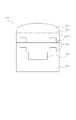
図1(b)は本発明に係る第1の実施形態である光学フィルタの上面図であり、図1(a)はA−A´の断面図である。 FIG. 1B is a top view of the optical filter according to the first embodiment of the present invention, and FIG. 1A is a cross-sectional view taken along line AA ′.
誘電体基板110の表面上には誘電体層130が設けられ、この誘電体基板110と誘電体層130との間には複数の金属構造体120が設けられている。
A
この金属構造体120は誘電体基板110の面内方向に孤立した状態で2次元的、かつ周期的に設けられており、金属構造体群として構成されている。なお、説明のため、第1の金属構造体群を構成する2つの第1の金属構造体について符号121と122を付している。
The
本発明に係る光学フィルタは、金属構造体単体により発現する局在プラズモン共鳴によるものであるが、金属構造体120を周期的に設けることは以下の点から好ましい。
The optical filter according to the present invention is based on localized plasmon resonance expressed by a single metal structure, but it is preferable to periodically provide the
すなわち、プラズモン共鳴が生じる際に、各金属構造体には電界が染み出すため、電界が染み出す範囲内に各金属構造体同士を配置すると、各金属構造体の共鳴条件は互いに影響を受けることになる。この影響を減少させるためには、金属構造体と該金属構造体に隣接する金属構造体とを電磁的に同等な関係となる位置、つまり周期的に配置することが好ましい。 That is, when plasmon resonance occurs, an electric field oozes out from each metal structure, so if the metal structures are arranged within the range where the electric field oozes, the resonance conditions of each metal structure are affected by each other. become. In order to reduce this influence, it is preferable that the metal structure and the metal structure adjacent to the metal structure are disposed at positions that are electromagnetically equivalent, that is, periodically.
このように各金属構造体を周期的に配置すれば、各金属構造体における共鳴条件のずれが抑制され、各構造体において同じ共鳴波長で同位相の局在プラズモン共鳴を誘起可能となる。この結果、共鳴ピークのディップが深く、ピーク幅が狭い透過スペクトルを得ることができる。また、回折光の発生を抑制できるために、透過スペクトル形状への影響も低減できる。 If each metal structure is periodically arranged in this way, a shift in resonance conditions in each metal structure is suppressed, and local plasmon resonance having the same phase can be induced in each structure at the same resonance wavelength. As a result, a transmission spectrum having a deep resonance peak dip and a narrow peak width can be obtained. In addition, since the generation of diffracted light can be suppressed, the influence on the transmission spectrum shape can also be reduced.
ところで、各金属構造体を近接しすぎると、各金属構造体の共鳴条件は互いに強く影響を受ける結果、所望の共鳴波長やスペクトル幅が得られず、透過率も低下する可能性がある。そのため、局在プラズモン共鳴の際に金属構造体の電界はその構造体自身の大きさ程度の距離まで染み出すことを考慮すると、金属構造体同士の間隔はその構造体の大きさ程度に離れていることが好ましい。 By the way, if the metal structures are too close to each other, the resonance conditions of the metal structures are strongly influenced by each other. As a result, a desired resonance wavelength and spectrum width cannot be obtained, and the transmittance may be lowered. Therefore, considering that the electric field of a metal structure leaks to a distance of about the size of the structure itself at the time of localized plasmon resonance, the distance between the metal structures is separated by about the size of the structure. Preferably it is.
また、より好ましくは、金属構造体同士の間隔は前述の電界の染み出しが重なり合わない程度に離れていること、つまり金属構造体同士の間隔が金属構造体自身の大きさの2倍程度以上離れていることが好適である。 More preferably, the distance between the metal structures is such that the aforementioned exudation of the electric field does not overlap, that is, the distance between the metal structures is about twice or more the size of the metal structure itself. It is preferred that they are separated.
一方、金属構造体同士の間隔が構造体自身の大きさの3倍程度に離れると、透過スペクトルのディップが浅くなってしまう。 On the other hand, when the distance between the metal structures is about three times the size of the structure itself, the dip of the transmission spectrum becomes shallow.
したがって、周期的に設けられている金属構造体同士の間隔として好適なのは、構造体自身の大きさの1倍以上であり、より好ましくは1倍以上3倍以下であり、より好ましくは2倍程度である。 Accordingly, the interval between the metal structures provided periodically is preferably 1 or more times the size of the structure itself, more preferably 1 to 3 times, and more preferably about 2 times. It is.
図1において、第1の金属構造体121は、第1の方向140に第1の長さ141を有し、かつ、第1の方向140と直交する第2の方向150に第2の長さ151を有している。ここで、第1の長さ141と第2の長さ151は例えば可視光領域における光の波長以下の長さに設定する。金属構造体に誘起されるプラズモンの波長は最低次のモード(双極子モード)の場合であっても、プラズモンの半波長が金属構造体の大きさと略同一になる。そのため、例えば可視光でプラズモンを励起され得る構造の大きさは可視光の励起波長よりも短くなることから、これらの長さを可視光領域における光の波長以下としている。
In FIG. 1, the
また、第1の長さ141と第2の長さ151をプラズモン共鳴波長以下(第1の波長以下)とすることも好ましい形態である。
It is also a preferred embodiment that the
ここでは、一例として、第1の金属構造体121は、第1の長さと第2の長さが同一である正方形状とし、一辺を120nmとしている。光学特性の設計容易性という点からは正方形状は好ましいが、円形状や楕円形状、その他多角形形状の金属も金属構造体として用いることができる。例えば、円形状ならば偏光依存性を抑制することが可能となり且つ作製精度も維持しやすいため好適である。
Here, as an example, the
正方形状でない金属構造体を用いた場合には、図18に示すように、第1の長さは符号1801、第2の長さは符号1802で示された長さとして取り扱う。
In the case of using a metal structure that is not square, the first length is handled as a
金属構造体の形状は、これに限定されるものではなく種々のものを取り得るが、第1の長さ、または第2の長さは、金属構造体の最大幅ととらえることもできる。 The shape of the metal structure is not limited to this, and various shapes can be taken. However, the first length or the second length can be regarded as the maximum width of the metal structure.
本実施形態では、金属構造体と、誘電体基板または誘電体層に入射する光とが共鳴することにより、金属構造体の表面に誘起される局在プラズモンによって、可視光領域における所定の波長(第1の波長)の透過率が極小値を示す。 In the present embodiment, the metal structure and the light incident on the dielectric substrate or the dielectric layer resonate, so that localized plasmons induced on the surface of the metal structure cause a predetermined wavelength in the visible light region ( The transmittance of the first wavelength is a minimum value.
図1に示した第1の金属構造体群において、金属構造体120が設けられている周期145および周期155は、可視光領域における光の波長以下、より好ましくはプラズモン共鳴波長以下(第1の波長以下)にすることも好適な形態である。注目している光の波長領域よりも金属構造体の周期が大きい場合には、高次の回折光が発生し、0次回折光の強度が低下する可能性があるからである。
In the first metal structure group illustrated in FIG. 1, the
また、金属構造体120が設けられている周期145および周期155は、第1の金属構造体群のプラズモン共鳴波長(第1の波長)より小さくすることも好ましい形態である。金属構造体の周期がプラズモン共鳴波長と近くなると、ウッズのアノマリを起こす波長の光がプラズモン共鳴と結合し、プラズモン共鳴によるピーク形状が先鋭化すると共に共鳴波長での透過率極小値の深さが浅くなってしまうからである。ここで、ウッズのアノマリとは、入射光が周期構造により回折され、回折光が金属周期構造表面の極近傍を表面と平行に伝播する現象のことをいう。
In addition, it is also preferable that the
ここでは、一例として、赤色の波長帯域にプラズモン共鳴を生じさせることを目的として、周期145および155は400nmとしている。
Here, as an example, the
また、第1の金属構造体121と122との間隔152は、第1の長さ141及び第2の長さ151よりも大きくすることも好ましい形態である。このような間隔に設定すれば、金属体構造体同士の間で近接場相互作用が強く生じることによるスペクトルピーク幅の拡大やピーク波長のシフト等を抑制することができる。
In addition, it is also preferable that the
また、金属構造体120の厚さ160を可視光領域における光の波長以下、好ましくはプラズモン共鳴波長以下(第1の波長以下)にすることも好適な形態である。フィルタを作製する際の微細加工プロセスにおいて、金属構造体の厚さを厚く設定しすぎると作製誤差が大きくなるからである。ここでは、一例として、厚さ160は30nmとしている。
In addition, it is also a preferable form that the
金属構造体120の材料としては、アルミニウム、金、銀、白金などを用いることができる。このうちアルミニウムは、銀と比較してプラズマ周波数が高く、物性的に可視域全体を網羅する光学特性のフィルタの設計が容易である(Ag:〜3.8eV(〜325nm)、Al:〜15eV(〜83nm))。
As a material of the
また、アルミニウムは、銀等と比較して酸化されにくく、化学的に安定であるため、長期間安定して所定の光学特性を発現できる。 In addition, since aluminum is less oxidized and chemically stable than silver or the like, it can stably exhibit predetermined optical characteristics for a long period of time.
さらに、アルミニウムは、銀と比較して誘電率の虚部が大きいため銀と比較して膜厚を薄くしても十分な遮光性を発現させることができ、また微細加工が容易である。 Furthermore, since aluminum has a larger imaginary part of dielectric constant than silver, sufficient light shielding properties can be exhibited even if the film thickness is made thinner than silver, and fine processing is easy.
加えて、アルミニウムは、白金のように化学的に極度に不活性であるためにドライエッチングによる微細加工が困難であるなどの難点も無い。 In addition, since aluminum is extremely chemically inert like platinum, there is no difficulty in that fine processing by dry etching is difficult.
なお、金属構造体120はアルミニウム、金、銀、白金を含む混合物や、合金であってもよい。
The
誘電体基板110の材料としては、例えば可視光領域の光を透過する材料である石英(二酸化ケイ素)、二酸化チタンなどの金属酸化物や、窒化シリコンなどの透過率が高い材料から適宜選択することができる。また、ポリカーボネートやポリエチレンテレフタレートなどの高分子材料も誘電体基板110の材料として用いることができる。
As a material of the
誘電体層130の材料としては、誘電体基板110と同様に、石英(二酸化ケイ素)、二酸化チタン、窒化シリコン等から適宜選択することができる。また、ポリカーボネートやポリエチレンテレフタレートなどの高分子材料も誘電体層130の材料として用いることができる。
The material of the
ここで、誘電体基板110と誘電体層130の誘電体率の差は5%以下であることが好ましい。誘電体基板110の誘電率と誘電体層130の誘電率が大きく異なると、金属構造体120と誘電体基板110の界面に生じるプラズモンの励起波長と、金属構造体120と誘電体層130の界面に生じるプラズモンの励起波長とが大きく異なるからである。この結果、所望以外の共鳴波長のピークや、ピーク幅の拡大が生じるおそれがある。
Here, the difference in dielectric constant between the
そのため、誘電体基板が有する誘電率と、誘電体層が有する誘電率とが同一であることがもっとも好ましい。 Therefore, it is most preferable that the dielectric constant of the dielectric substrate and the dielectric constant of the dielectric layer are the same.
また誘電体層の厚みから金属構造体120の厚さ160を減じた厚さ170が厚すぎないことが好ましい。誘電体層の厚みが厚すぎると、誘電体層130が一種のファブリペロ−共振器を構成するため、透過スペクトルに微細なディップが多数あらわれてしまう懸念があるためである。
Further, it is preferable that the
そのため、例えば金属構造体120のプラズモン共鳴の半値全幅の波長範囲内にファブリペロー共振器の共振器モードが存在しないことが好適である。
Therefore, for example, it is preferable that the resonator mode of the Fabry-Perot resonator does not exist in the wavelength range of the full width at half maximum of the plasmon resonance of the
このためには少なくとも共振器モードの間隔(FSR)がプラズモン共鳴の半値全幅よりも広いことが必要であり、その条件は以下であらわされる。 For this purpose, at least the resonator mode interval (FSR) needs to be wider than the full width at half maximum of plasmon resonance, and the condition is expressed as follows.

ただし、λresは金属構造体のプラズモン共鳴波長、nは誘電体層の屈折率、ΔλFWは金属構造体の共鳴スペクトルの半値全幅である。 Where λ res is the plasmon resonance wavelength of the metal structure, n is the refractive index of the dielectric layer, and Δλ FW is the full width at half maximum of the resonance spectrum of the metal structure.
ここで、式中のdは誘電体層の厚さに相当している。したがって、たとえば典型的にはプラズモン共鳴の半値全幅は100nmであるから、プラズモン共鳴の波長を650nm、誘電体層の屈折率を1.46とすると、dは1447nmと算出される。このため、注目波長領域が650nm±50nmである場合、この波長域でFSRを100nm以上確保するためには、誘電体層の厚みはこのd以下である必要がある。 Here, d in the formula corresponds to the thickness of the dielectric layer. Therefore, for example, typically, the full width at half maximum of plasmon resonance is 100 nm. Therefore, when the wavelength of plasmon resonance is 650 nm and the refractive index of the dielectric layer is 1.46, d is calculated to be 1447 nm. For this reason, when the wavelength region of interest is 650 nm ± 50 nm, the thickness of the dielectric layer needs to be less than or equal to d in order to secure an FSR of 100 nm or more in this wavelength region.
また、ファブリペロー共振器の共振器モードが注目波長域よりも短い波長域にしか現れないようにすることも好ましい形態である。 It is also a preferable form that the resonator mode of the Fabry-Perot resonator appears only in a wavelength region shorter than the wavelength region of interest.
ファブリペロー共振器の共振器モードは、共振器長の2倍と等しい波長において出現する。注目波長域を金属構造体の共鳴幅内の波長域とする場合、注目波長域の最短波長は共鳴波長から共鳴の半値半幅を減じた値である。そのため、この波長よりもファブリペロー共振器の共振器モードが短くなるために、誘電体層の厚さは以下の式で示す値d以下にする必要がある。 The resonator mode of the Fabry-Perot resonator appears at a wavelength equal to twice the resonator length. When the wavelength region of interest is a wavelength region within the resonance width of the metal structure, the shortest wavelength of the wavelength region of interest is a value obtained by subtracting the half width of resonance from the resonance wavelength. Therefore, since the resonator mode of the Fabry-Perot resonator becomes shorter than this wavelength, the thickness of the dielectric layer needs to be equal to or less than the value d represented by the following formula.
![]()
![]()
ただし、λresは金属構造体のプラズモン共鳴波長、nは誘電体層の屈折率、ΔλHWは金属構造体の共鳴スペクトルの半値半幅である。 Where λ res is the plasmon resonance wavelength of the metal structure, n is the refractive index of the dielectric layer, and Δλ HW is the half width at half maximum of the resonance spectrum of the metal structure.
例えば、共鳴波長が450nm、共鳴の半値半幅が50nmの場合、屈折率を1.46とするとdは137nmと算出される。このため、可視光域最短波長である400nmよりも短波長側にファブリペロー共振器モードが現れないようにするためには、誘電体層の厚みはこのd以下にすることが好ましい。 For example, when the resonance wavelength is 450 nm and the half width of resonance is 50 nm, d is calculated as 137 nm when the refractive index is 1.46. Therefore, in order to prevent the Fabry-Perot resonator mode from appearing on the shorter wavelength side than 400 nm, which is the shortest wavelength in the visible light region, it is preferable that the thickness of the dielectric layer be less than or equal to this d.
一方、誘電体層の厚みが薄すぎることは余り好適ではなく、ある程度の厚みを有することが好適である。つまり誘電体層の厚みから金属構造体120の厚みを減じた厚さ170が、金属構造体120が有する第1の長さ141や第2の長さ151以上であることが好適である。また少なくとも厚さ170は100nm程度はあることが好ましい。
On the other hand, it is not so preferable that the thickness of the dielectric layer is too thin, and it is preferable to have a certain thickness. That is, it is preferable that the
これは金属構造体120が発生する近接場の広がりが、典型的には金属構造体120自身の大きさ程度もしくは100nm程度であるためである。金属構造体120の表面から金属構造体120が発生する近接場領域程度の距離内の空間が誘電体層で占められていれば、金属構造体120が発生する近接場領域内に異物等が混入し、金属構造体120の光学特性が変化することを抑制できる。
This is because the expansion of the near field generated by the
(計算結果)
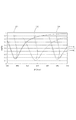
図2は、上記の構造を用いて数値計算を行なった結果を示したものである。すなわち、金属構造体としてアルミニウムを用いて、第1の長さと第2の長さを120nm、周期400nm、厚さ30nmとした光学フィルタである。この光学フィルタの透過スペクトルは透過スペクトル201のようになり、波長650nm付近の光を強く吸収する光学フィルタとして機能していることがわかる。
(Calculation result)
FIG. 2 shows the result of numerical calculation using the above structure. That is, the optical filter uses aluminum as the metal structure and has a first length and a second length of 120 nm, a period of 400 nm, and a thickness of 30 nm. The transmission spectrum of this optical filter is the
波長650nmは赤色の帯域であるため、Redの頭文字をとって光学フィルタRとする。この光学フィルタは赤色の波長を反射、吸収するため、透過スペクトルとしては、赤色の補色である青緑色が観察される。 Since the wavelength of 650 nm is a red band, the acronym Red is used as the optical filter R. Since this optical filter reflects and absorbs red wavelengths, blue-green, which is a complementary color of red, is observed as a transmission spectrum.
さらに、金属構造体の径や周期を変化させることによって、透過スペクトルの波長、スペクトル幅、強度を変化させることも可能である。 Furthermore, the wavelength, spectrum width, and intensity of the transmission spectrum can be changed by changing the diameter and period of the metal structure.
例えば、長さを100nm、周期を310nm、厚さを30nmとすることで、可視域の緑(波長550nm)付近に吸収がある透過スペクトル202を有する光学フィルタを構成できる。これを光学フィルタGとする。この光学フィルタGの透過スペクトルを観察すると、緑色の補色である赤紫色を観察することができる。
For example, by setting the length to 100 nm, the period to 310 nm, and the thickness to 30 nm, an optical filter having a
同様に、長さを70nm、周期を250nm、厚さを30nmにすることで可視域の青(波長450nm)付近に吸収がある透過スペクトル203を有する光学フィルタを構成できる。これを光学フィルタBとする。このフィルタBの透過スペクトルを観察すると、青色の補色である黄色を観察することができる。
Similarly, by setting the length to 70 nm, the period to 250 nm, and the thickness to 30 nm, an optical filter having a
なお、本実施形態に係る光学フィルタの反射スペクトルは、透過率が極小値を示す波長近傍で反射率が極大値となる。そのため、本実施形態に係る光学フィルタは、透過フィルタとしてのみならず、所望の波長で反射率を増加する反射フィルタとして用いることも可能である。 Note that the reflection spectrum of the optical filter according to the present embodiment has a maximum reflectance in the vicinity of the wavelength at which the transmittance is a minimum value. Therefore, the optical filter according to the present embodiment can be used not only as a transmission filter but also as a reflection filter that increases the reflectance at a desired wavelength.
(設計指針)
以下、金属構造体群を構成するパラメータと光学特性の関係について説明する。
(Design guidelines)
Hereinafter, the relationship between the parameters constituting the metal structure group and optical characteristics will be described.
金属構造体に誘起される局在プラズモン共鳴は、金属構造体内での自由電子のプラズマ振動に伴う電荷密度分布であり、この電荷密度分布や金属構造体の光学特性は構造体の形状に影響される。 Localized plasmon resonance induced in a metal structure is a charge density distribution associated with plasma oscillation of free electrons in the metal structure. The charge density distribution and the optical characteristics of the metal structure are affected by the shape of the structure. The
例えば、金属構造体に照射される光の偏光方向と直交する方向の金属構造体の長さ、金属構造体の厚さ、及び金属構造体を配置する周期を一定にしたまま、偏光方向の金属構造体の長さを長くすると、共鳴波長は長波長側に移行する。 For example, while maintaining the length of the metal structure in the direction orthogonal to the polarization direction of the light irradiated to the metal structure, the thickness of the metal structure, and the period of arranging the metal structure, the metal in the polarization direction When the length of the structure is increased, the resonance wavelength shifts to the longer wavelength side.
このため、金属構造体の局在プラズモン共鳴の波長を長波長側に発生させるためには金属構造体の偏光方向の長さを長くすれば良いことが分かる。この傾向を図17に示す。図17(b)に示した表により、金属微粒子の偏光方向の長さが長くなるにつれて、共鳴波長が長波長に移行するだけでなく、ピーク幅は広がり、吸収ピークでの透過率は低下することが分かる。なお、光学フィルタに入射する光の偏光は厳密に金属微粒子の長手方向もしくは短手方向に沿っていることは必ずしも必要ない。 For this reason, it can be seen that in order to generate the wavelength of localized plasmon resonance of the metal structure on the longer wavelength side, the length of the polarization direction of the metal structure may be increased. This tendency is shown in FIG. According to the table shown in FIG. 17B, as the length of the polarization direction of the metal fine particles increases, not only the resonance wavelength shifts to a longer wavelength, but also the peak width widens and the transmittance at the absorption peak decreases. I understand that. Note that the polarization of light incident on the optical filter does not necessarily have to be strictly along the longitudinal direction or the lateral direction of the metal fine particles.
また、図19(a)に示すように、偏光と直交方向の金属構造体の長さが長くなるにつれて、共鳴波長は短波長側に移行する。また、図19(b)により、偏光と直交方向の金属構造体の長さが長くなるにつれて共鳴幅は広がり、共鳴波長での透過率は減少する傾向にあることが分かる。 Further, as shown in FIG. 19A, the resonance wavelength shifts to the short wavelength side as the length of the metal structure in the direction orthogonal to the polarization becomes longer. Further, FIG. 19B shows that the resonance width increases and the transmittance at the resonance wavelength tends to decrease as the length of the metal structure perpendicular to the polarization increases.
また、図20(a)および(b)に示すように、金属構造体の厚さが増大すると共鳴波長は短波長化するともに、共鳴波長での透過率は減少し、共鳴幅は若干減少する傾向にあることが分かる。 As shown in FIGS. 20A and 20B, when the thickness of the metal structure is increased, the resonance wavelength is shortened, the transmittance at the resonance wavelength is decreased, and the resonance width is slightly decreased. It turns out that there is a tendency.
このことを用い、図22に示すように、スペクトル形状を透過スペクトル2201から透過スペクトル2202に改善することが可能である。
Using this, the spectral shape can be improved from the
透過スペクトル2201では波長530nm近傍にウッズのアノマリによる鋭いディップがスペクトルに存在している。透過スペクトル2201は、一辺150nmの正方形、膜厚90nmのアルミニウムからなる金属ドットを周期400nmで正三角格子状に配列した場合の光学スペクトルである。一方、透過スペクトル2202は膜厚を150nmに増大した場合のものである。
In the
すなわち、膜厚を増大させることによりドットアレイの共鳴波長を短波長側にシフトさせ、ウッズのアノマリの鋭いディップと重複させることで、スペクトル形状を単峰化させると共に共鳴幅を狭帯化させることもできる。 That is, by increasing the film thickness, the resonance wavelength of the dot array is shifted to the short wavelength side, and overlapping with the sharp dip of the Woods anomaly makes the spectrum shape unimodal and narrows the resonance width. You can also.
このように金属膜厚を所定の値にすることで、スペクトル上から好ましく無いディップを隠すことも可能である。 In this way, by setting the metal film thickness to a predetermined value, it is possible to hide an undesirable dip from the spectrum.
また、図21(a)および(b)に示すように、金属構造体が設けられた周期が増大すると、共鳴波長は長波長化するとともに、共鳴波長での透過率は増大し、共鳴幅は減少していく傾向にあることが分かる。 Further, as shown in FIGS. 21A and 21B, when the period in which the metal structure is provided increases, the resonance wavelength becomes longer, the transmittance at the resonance wavelength increases, and the resonance width becomes It can be seen that it tends to decrease.
このような知見を基にして、金属構造体と金属構造体群のパラメータの最適化を図ることも可能であり、所望の波長に共鳴波長を有する光学フィルタを設計することが可能である。 Based on such knowledge, it is possible to optimize the parameters of the metal structure and the metal structure group, and it is possible to design an optical filter having a resonance wavelength at a desired wavelength.
本発明者らの検討によれば、光学フィルタの共鳴波長を赤色の帯域(550nm以上から650nm未満)とするためには、金属構造体の第1の長さと第2の長さを110nm以上160nm以下の範囲に設定する必要がある。また、金属構造体の厚さを10nm以上200nm以下の範囲とし、かつ周期を340nm以上450nm以下の範囲に設定する必要がある。 According to the study by the present inventors, in order to set the resonance wavelength of the optical filter to a red band (550 nm or more to less than 650 nm), the first length and the second length of the metal structure are set to 110 nm or more and 160 nm. It is necessary to set the following range. Further, it is necessary to set the thickness of the metal structure in the range of 10 nm to 200 nm and the period in the range of 340 nm to 450 nm.
また、光学フィルタの共鳴波長を緑色の帯域(450nm以上から550nm未満)とするためには、金属構造体の第1の長さと第2の長さを90nm以上130nm未満の範囲に設定する必要がある。また、金属構造体の厚さを10nm以上200nm以下の範囲とし、かつ金属構造体が設けられている周期を260nm以上340nm以下、好ましくは270nm以上330nm以下の範囲に設定する必要がある。 Further, in order to set the resonance wavelength of the optical filter to a green band (from 450 nm to less than 550 nm), it is necessary to set the first length and the second length of the metal structure within a range of 90 nm to less than 130 nm. is there. In addition, the thickness of the metal structure must be in the range of 10 nm to 200 nm, and the period in which the metal structure is provided must be set in the range of 260 nm to 340 nm, preferably 270 nm to 330 nm.
また、光学フィルタの共鳴波長を青色の帯域(350nm以上から450nm未満)とするためには、金属構造体の第1の長さと第2の長さを60nm以上100nm未満の範囲に設定する必要がある。また、金属構造体の厚さを10nm以上200nm以下の範囲とし、かつ金属構造体が設けられている周期を180nm以上280nm以下、好ましくは200nm以上270nm以下の範囲に設定する必要がある。 Further, in order to set the resonance wavelength of the optical filter to a blue band (from 350 nm to less than 450 nm), it is necessary to set the first length and the second length of the metal structure in the range of 60 nm to less than 100 nm. is there. In addition, the thickness of the metal structure must be in the range of 10 nm to 200 nm, and the period in which the metal structure is provided must be set in the range of 180 nm to 280 nm, preferably 200 nm to 270 nm.
本実施形態の光学フィルタは、可視光領域に吸収または反射のピーク波長を有するものとして説明した。一方、可視光領域の設計値に比べて金属構造体の大きさを小さく、周期を小さくすることで近紫外領域の光学フィルタとすることができる。同様に、金属構造体の大きさを大きく、周期を大きくすることで近赤外領域の光学フィルタとすることも可能である。 The optical filter of the present embodiment has been described as having an absorption or reflection peak wavelength in the visible light region. On the other hand, an optical filter in the near ultraviolet region can be obtained by reducing the size and the period of the metal structure compared to the design value in the visible light region. Similarly, an optical filter in the near infrared region can be obtained by increasing the size of the metal structure and increasing the period.
(第2の実施形態:ベイヤー配列)
本実施形態では、ベイヤー配列となっているRGBフィルタについて説明する。
(Second embodiment: Bayer array)
In the present embodiment, an RGB filter having a Bayer array will be described.
図3において、領域301には例えば前述の光学フィルタR(透過スペクトル201)を配置し、領域302には光学フィルタG(透過スペクトル202)、領域303には光学フィルタB(透過スペクトル203)を配置する。このような配置にすることで本発明に係るフィルタを用いて、ベイヤー配列のカラーフィルタを構成することが可能である。
In FIG. 3, for example, the optical filter R (transmission spectrum 201) described above is disposed in a
なお、このカラーフィルタは、撮像素子用のカラーフィルタとして用いることができる。この場合、領域301等は1画素に対応した面積となるが、領域301等は光電変換素子(光電変換部)が占める領域よりも大きい面積を有していても良い。
This color filter can be used as a color filter for an image sensor. In this case, the
本実施形態では、領域ごとに金属構造体の大きさが異なり、かつ金属構造体が設けられている周期も異なっているがこの構成に限るものではない。例えば、金属構造体の周期だけが異なる金属構造体群が各領域に配置されていても良い。また、金属構造体の大きさだけが異なる金属構造体群が各領域に配置されていても良い。 In the present embodiment, the size of the metal structure is different for each region and the period in which the metal structure is provided is different, but the present invention is not limited to this configuration. For example, metal structure groups that differ only in the period of the metal structure may be arranged in each region. Moreover, the metal structure group from which only the magnitude | size of a metal structure differs may be arrange | positioned in each area | region.
つまり、第1の金属構造体群を2つ以上有し、第1の金属構造体が設けられている周期は互いに異なっており、前記第1の金属構造体群は前記誘電体基板表面の相異なる領域に配置されていても良い。 That is, two or more first metal structure groups are provided, and the periods in which the first metal structures are provided are different from each other, and the first metal structure group is a phase on the surface of the dielectric substrate. They may be arranged in different areas.
また、第1の金属構造体群を構成する第1の金属構造体とは異なる形状である第2の金属構造体からなる第2の金属構造体群が各領域に配置されていても良い。すなわち、第2の金属構造体は、第1の方向に第3の長さを有し、第2の方向に第4の長さを有し、第3の長さは第1の金属構造体が有する第1の長さと異なるか、または第4の長さは第1の金属構造体が有する第2の長さと異なっている。なお、第3の長さと第4の長さは第2の波長以下であることが好ましい形態である。 Moreover, the 2nd metal structure group which consists of a 2nd metal structure which is a shape different from the 1st metal structure which comprises a 1st metal structure group may be arrange | positioned in each area | region. That is, the second metal structure has a third length in the first direction, has a fourth length in the second direction, and the third length is the first metal structure. Is different from the first length of the first metal structure or the fourth length is different from the second length of the first metal structure. The third length and the fourth length are preferably equal to or shorter than the second wavelength.
この結果、第2の金属構造体群は、第1の構造体群の共鳴波長(第1の波長)とは異なる波長(第2の波長)で光の透過率を減少させることができる。 As a result, the second metal structure group can reduce the light transmittance at a wavelength (second wavelength) different from the resonance wavelength (first wavelength) of the first structure group.
なお、本明細書において、第1の金属構造体群と第2の金属構造体群とは、構造体群を構成する金属構造体の形状が異なることを意味する。すなわち、金属構造体の周期が異なっていても、形状が同じであれば、第1の金属構造体群という用語を用いる。また、金属構造体の形状が異なっていれば、周期が同一であっても異なっていても、第2の金属構造体群という用語を用いる。 In the present specification, the first metal structure group and the second metal structure group mean that the shapes of the metal structures constituting the structure group are different. That is, even if the periods of the metal structures are different, the term “first metal structure group” is used if the shapes are the same. Further, if the shapes of the metal structures are different, the term “second metal structure group” is used regardless of whether the periods are the same or different.
(第3の実施形態:三角格子)
図16は金属構造体が三角格子状に配列されている実施形態を示した図である。三角格子配列にした場合には、格子の単位ベクトル成分が直交していないため、正方格子状の配列と比較してフィルタの光学特性の入射光偏光に対する依存性を軽減することが可能となる。
(Third embodiment: triangular lattice)
FIG. 16 is a view showing an embodiment in which metal structures are arranged in a triangular lattice shape. In the case of the triangular lattice arrangement, the unit vector components of the lattice are not orthogonal, so that the dependence of the optical characteristics of the filter on the incident light polarization can be reduced as compared with the square lattice arrangement.
このような三角格子配列は、正方格子状に配列されている複数の金属構造体群が重複した領域に配置されていると表現することもできる。 Such a triangular lattice arrangement can also be expressed as a plurality of metal structure groups arranged in a square lattice are arranged in an overlapping region.
すなわち、第1の金属構造体1601により構成される第1の金属構造体群1602と、第2の金属構造体1603により構成される第2の金属構造体群1604とは、重複した領域に配置していると表現することが可能である。
That is, the first
(第4の実施形態:2つ以上の構造体群の重複)
本実施形態でも、第3の実施形態と同じく、複数の金属構造体群が重複して配置されている例について説明する。
(Fourth embodiment: overlap of two or more structures)
In the present embodiment as well, as in the third embodiment, an example in which a plurality of metal structure groups are arranged in an overlapping manner will be described.
図4(a)は、周期が異なる第1の金属構造体群が重複して配置されている例を示したものである。第1の金属構造体群402を構成する第1の金属構造体401が周期405で設けられており、第1の金属構造体群404を構成する第1の金属構造体403は周期406で設けられている。このように、本実施形態では、金属構造体の配列周期が互いに異なることから、2つの金属構造体群が個々に有する光学特性を同時に発現させることが可能となる。
FIG. 4A shows an example in which the first metal structure groups having different periods are arranged in an overlapping manner. The
すなわち、図4(a)の光学フィルタは、前記誘電体基板の面内方向に、前記第1の金属構造体群を2つ以上有し、この2つ以上の第1の金属構造体群を構成する第1の構造体が設けられている周期は互いに異なっている。また、この2つ以上の第1の金属構造体群は重複した領域に配置されている。 That is, the optical filter of FIG. 4A has two or more of the first metal structure groups in the in-plane direction of the dielectric substrate, and the two or more first metal structure groups are included. The periods in which the first structural body is provided are different from each other. In addition, the two or more first metal structure groups are arranged in overlapping regions.
また、図4(b)は、第1の金属構造体と第2の金属構造体とが重複した領域に配置されている例を示したものである。第1の金属構造体407は第1の金属構造体群を構成し、第2の金属構造体408は第2の金属構造体群を構成する。このように金属構造体群を構成する金属構造体の形状が異なることから、2つの金属構造体群が有する個々の光学特性を同時に発現させることが可能となる。
FIG. 4B shows an example in which the first metal structure and the second metal structure are arranged in an overlapping region. The
すなわち、図4(b)の光学フィルタは、第1の金属構造体群とは別に、誘電体基板の面内方向に、複数の第2の金属構造体を孤立した状態で2次元的、かつ周期的に設けた第2の金属構造体群を有している。この第2の金属構造体は、第1の方向に第3の長さを有し、かつ第2の方向に第4の長さを有し、第3の長さと第4の長さは前記第1の波長とは異なる第2の波長以下である。この第3の長さは第1の長さと異なるか、または第4の長さは前記第2の長さと異なっており、第1の金属構造体群と、第2の金属構造体群とは重複した領域に配置されている。この結果、第1の金属構造体の共鳴波長(第1の波長)と、第2の金属構造体の共鳴波長(第2の波長)が異なっている。 That is, the optical filter of FIG. 4B is two-dimensionally in a state where a plurality of second metal structures are isolated in the in-plane direction of the dielectric substrate, separately from the first metal structure group. It has the 2nd metal structure group provided periodically. The second metal structure has a third length in the first direction and a fourth length in the second direction, and the third length and the fourth length are It is below the 2nd wavelength different from the 1st wavelength. The third length is different from the first length, or the fourth length is different from the second length. The first metal structure group and the second metal structure group are: Arranged in overlapping areas. As a result, the resonance wavelength (first wavelength) of the first metal structure is different from the resonance wavelength (second wavelength) of the second metal structure.
(第5の実施形態:単列フィルタ)
本実施形態では、単列フィルタについて説明する。
(Fifth embodiment: single-row filter)
In the present embodiment, a single column filter will be described.
図5において、第1の金属構造体509は第1の方向502に第1の長さ504を有し、かつ第1の方向502と直交する方向に第2の方向503に第2の長さ505を有する。そして、第1の金属構造体509は第1の方向502に周期的に配列されており、これにより第1の金属構造体群501を構成している。
In FIG. 5, the
また、第2の金属構造体510は第1の方向502に第3の長さ507を有し、かつ第2の方向503に第4の長さ508を有する。そして、第2の金属構造体510は第1の方向502に周期的に配列されており、これにより第2の金属構造体群506を構成している。
The
これらの金属構造体群501と506はそれぞれ異なる波長の光に対してプラズモン共鳴を生じ、その結果異なる波長の光の透過率を減少させることができる。そのため、図5に示した構造を有する光学フィルタは、光の照射位置によって透過率が低下する波長が変化するため、このフィルタを分光などに用いることが可能である。
These
なお、図5に示した金属構造体509は第1の方向に有する周期と、金属構造体510が第1の方向に有する周期とが異なっているが、図6に示すように周期を同一にしても良い。
Note that the period that the
すなわち、本実施形態に係る光学フィルタは、複数の金属構造体を前記誘電体基板の面内方向に孤立した状態で設けて構成された第1の金属構造体群と第2の金属構造体群とを有している。また、第1の金属構造体群と、第2の金属構造体群とは誘電体基板表面の相異なる領域に配置され、第1の金属構造体は、第1の方向に周期的に配置されている。また、この第1の金属構造体の第1の長さと第2の長さは、第1の波長以下の長さである。また、第2の金属構造体群を構成する第2の金属構造体は、前記第1の方向に周期的に配置されている。また、この第2の金属構造体は、第1の方向に第3の長さを有し、かつ第2の方向に第4の長さを有し、第3の長さと第4の長さは、第1の波長とは異なる第2の波長以下の長さである。そして、この第1の長さと第3の長さが異なるか、または、第2の長さと第4の長さが異なっている結果、第1の金属構造体の共鳴波長(第1の波長)と、第2の金属構造体の共鳴波長(第2の波長)が異なっている。 That is, the optical filter according to the present embodiment includes a first metal structure group and a second metal structure group configured by providing a plurality of metal structures in an isolated state in the in-plane direction of the dielectric substrate. And have. The first metal structure group and the second metal structure group are disposed in different regions on the surface of the dielectric substrate, and the first metal structure body is periodically disposed in the first direction. ing. Further, the first length and the second length of the first metal structure are equal to or shorter than the first wavelength. In addition, the second metal structures constituting the second metal structure group are periodically arranged in the first direction. The second metal structure has a third length in the first direction and a fourth length in the second direction, and the third length and the fourth length. Is a length equal to or shorter than a second wavelength different from the first wavelength. Then, as a result of the difference between the first length and the third length, or the difference between the second length and the fourth length, the resonance wavelength (first wavelength) of the first metal structure. And the resonance wavelength (second wavelength) of the second metal structure is different.
(第6の実施形態:積層型の光学フィルタ)
本実施形態では、積層された光学フィルタについて説明する。
(Sixth embodiment: multilayer optical filter)
In the present embodiment, the stacked optical filters will be described.
図7において、誘電体基板701上には第1の金属構造体群702が形成され、更に第1の誘電体層703に覆われている。そして、第1の誘電体層703上には第2の金属構造体群704が配置され、更にその上に第2の誘電体層(他の誘電体層)705が形成されている。
In FIG. 7, a first
これにより、図2で示した透過スペクトル201と透過スペクトル203の積で表現される透過スペクトルの光学フィルタとすることも可能である。例えば、光学フィルタRと光学フィルタBのフィルタを積層することで、光学フィルタRの透過率と光学フィルタBの積の透過スペクトルを有する光学フィルタとすることができる。このフィルタは波長550nm付近に透過率の最大値が生じる。このように単層では補色のフィルタとして機能するフィルタを、積層することで原色のフィルタとして機能させることも可能になる。
Thereby, an optical filter having a transmission spectrum expressed by the product of the
第1の金属構造体群702と、第2の金属構造体群704の構成は面内の配列の周期が異なるか、あるいは金属構造体の形状が異なっている。
The configurations of the first
第1の金属構造体群702と、第2の金属構造体群704の構成が異なることにより、これら各層は互いに異なる波長に対してプラズモン共鳴を生じる。その結果、本実施形態の光学フィルタは少なくとも二つの波長に対して透過率が極小になる。
Since the first
このことはつまり前述の二つの極小となる波長の間の波長を通すバンドパスフィルタとしての機能を有していることを意味する。 This means that it has a function as a band-pass filter that passes a wavelength between the two minimum wavelengths.
したがって、単層である第1の金属構造体群702、と第2の金属構造体群704は補色フィルタの機能を有しているが、これらを積層構成することで両者の特性を併せもつ原色フィルタ機能を発現することができる。
Therefore, the first
すなわち、本実施形態に係る積層型の光学フィルタは、誘電体層表面の上に、更に他の誘電体層が形成された積層型の光学フィルタである。そして、誘電体層表面と他の誘電体層との間に、複数の第2の金属構造体を前記誘電体層表面の面内方向に孤立した状態で2次元的、かつ周期的に設けた第2の金属構造体群を有している。第2の金属構造体群を構成する第2の金属構造体は、第1の方向に第3の長さを有し、かつ第2の方向に第4の長さを有し、第3の長さと第4の長さは、第1の波長とは異なる第2の波長以下の長さである。第1の長さと第3の長さが異なるか若しくは第2の長さと第4の長さが異なるか、又は、第2の金属構造体が設けられている周期と第1の金属構造体が設けられている周期とが異なっている。これにより、第2の金属構造体群は、第1の構造体群の共鳴波長(第1の波長)とは異なる共鳴波長(第2の波長)における透過率を減少させることができる。 That is, the multilayer optical filter according to the present embodiment is a multilayer optical filter in which another dielectric layer is further formed on the surface of the dielectric layer. A plurality of second metal structures are provided two-dimensionally and periodically between the dielectric layer surface and another dielectric layer in a state of being isolated in the in-plane direction of the dielectric layer surface. A second metal structure group is included. A second metal structure forming the second metal structure group is in a first direction having a third length of, and a fourth length of the second direction, the third The length and the fourth length are not more than the second wavelength, which is different from the first wavelength. The first length is different from the third length or the second length is different from the fourth length, or the period in which the second metal structure is provided and the first metal structure is The provided period is different. As a result, the second metal structure group can reduce the transmittance at a resonance wavelength ( second wavelength) different from the resonance wavelength (first wavelength) of the first structure group.
なお、本実施形態に係る積層型の光学フィルタにおいては、近接場相互作用が殆ど生じない積層間隔で積層することも好ましい形態である。具体的には、100nm以上の積層間隔とすることが好ましい。 In the laminated optical filter according to the present embodiment, it is also a preferred form that the laminated optical filters are laminated at a lamination interval in which almost no near-field interaction occurs. Specifically, the stacking interval is preferably 100 nm or more.
実施例1では、RGBの吸収・反射フィルタの作製方法と光学特性について説明する。 In Example 1, an RGB absorption / reflection filter manufacturing method and optical characteristics will be described.
図8(a)は厚さ525μmの石英基板からなる誘電体基板801の表面に、金属薄膜層802として厚さ30nmのアルミニウムを蒸着し、その上に電子線描画(EB)用レジスト803を塗布により形成したものである。なお、金属薄膜層802の成膜方法は蒸着に限るものでなく、スパッタリング等であってもよい。
In FIG. 8A, 30 nm thick aluminum is deposited as a metal
次に、EB描画装置を用いて、レジスト803をパターニングする。レジストパターンの形状は、一辺が約120nmの正方形であり、周期約400nmで正方格子状に配列した形状を作製する。このレジストパターンをエッチングマスクとして、塩素と酸素の混合気体のプラズマでドライエッチングすることで金属薄膜構造体804を形成することができる。なお、ドライエッチングガスは塩素と酸素に限るものではなく、アルゴンやその他のガスでも良い。
Next, the resist 803 is patterned using an EB drawing apparatus. The resist pattern has a square shape with a side of about 120 nm and is arranged in a square lattice pattern with a period of about 400 nm. With this resist pattern as an etching mask, the metal
また、エッチングマスクの作製方法はEB描画に限るものではなく、フォトリソグラフィー等でも良い。さらに、金属薄膜層802のパターニング方法は、誘電体基板801上にEB描画やフォトリソグラフィ−等によりレジストパターンを形成し、金属薄膜層802を成膜した後にリフトオフプロセスにより形成しても良い。加えて、収束イオンビーム加工装置(FIB加工装置)を用いて、金属薄膜層802を直接加工しても良い。
Further, the etching mask manufacturing method is not limited to EB drawing, and photolithography or the like may be used. Further, the metal
次に、金属薄膜構造体804の上に、誘電体層805として厚さ300nmの石英薄膜をスパッタリングにより成膜する。このようにして形成された光学フィルタを図8(b)に示す。なお、成膜方法は、スパッタリングに限るものではなく、CVDによる成膜やさらにはSOGなどを塗布しても良い。
Next, a quartz thin film having a thickness of 300 nm is formed as a
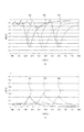
図9(a)には、このようにして作製した光学フィルタの透過スペクトルを示す。数値計算により透過スペクトルRは符号901のように求まり、本フィルタは波長650nm付近に透過率の最小値(吸収ピーク)を持つことが分かる。吸収ピークを示す波長は可視域の赤色に対応するため、本フィルタは赤を吸収する補色フィルタとして機能することがわかる。 FIG. 9A shows a transmission spectrum of the optical filter thus manufactured. By numerical calculation, the transmission spectrum R is obtained as indicated by reference numeral 901, and it can be seen that this filter has a minimum transmittance (absorption peak) near the wavelength of 650 nm. Since the wavelength showing the absorption peak corresponds to red in the visible range, it can be seen that this filter functions as a complementary color filter that absorbs red.
また、金属薄膜構造体804の径を約100nm、厚さを約30nm、周期を約310nmで配列することで符号902で示される透過スペクトルGが得られる。同様に、径を約70nm、厚さを30nm、周期を約250nmとすることで符号903で示される透過スペクトルBが得られる。これらはそれぞれRGBを吸収する光フィルタであり、補色フィルタとして機能する。
Further, by arranging the metal
また、本実施例のフィルタの反射スペクトルは、透過率が最小になる波長とほぼ同じ波長で反射率が最大になる。 Further, the reflection spectrum of the filter of the present embodiment has the maximum reflectance at substantially the same wavelength as the wavelength at which the transmittance is minimized.
そのため、図9(b)に示すように、本実施例の光学フィルタは、反射フィルタとして用いることで、透過スペクトルRを有するフィルタからは符号904で示される反射スペクトルRを得ることができる。同様に、透過スペクトルGを有するフィルタは符号905で示される反射スペクトルG、透過スペクトルBを有するフィルタは符号906で示される反射スペクトルBを得ることができる。このように、これらの光学フィルタはそれぞれ可視域の赤、緑、青の反射率を増加させる光学フィルタとして機能させることが可能である。
Therefore, as shown in FIG. 9B, by using the optical filter of this embodiment as a reflection filter, a reflection spectrum R indicated by
なお、本実施例では金属構造体が正方格子状に配列している例を用いて説明したが、三角格子配列にしてもよい。 In the present embodiment, the example in which the metal structures are arranged in a square lattice shape has been described. However, a triangular lattice arrangement may be used.
また、誘電体層805の厚みは300nmに限るものではない。より薄く作製しても構わない。金属構造体が生成する近接場領域の広さを誘電体層でカバーできるように、100nm程度もしくはそれ以上であることが好適である。
Further, the thickness of the
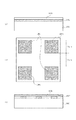
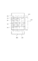
実施例2ではベイヤー配列のRGBフィルタの作製方法と光学特性について説明する。図10(a)は厚さ525μmの石英基板からなる誘電体基板1001の表面に、金属薄膜層1002として厚さ20nmのアルミニウムを蒸着し、その上にレジスト1003を塗布したものである。
In
次に、EB描画装置を用いて、レジスト1003をパターニングする。レジストパターンの形状は、一辺が約130nmの正方形を周期約380nmで正方格子状に配列した形状を約10μm角にパターニングした部分をパターン部A1004とする。また、一辺が約110nmの正方形を周期約280nmで正方格子状に配列した形状をパターン部B1005とし、一辺が約80nmの正方形を周期約200nmで正方格子状に配列した形状をパターン部C1006とする。これらの各パターン部を10μmの隙間を空けて図10(b)のように配置した構造を作製する。このレジストパターンをエッチングマスクとして、塩素と酸素の混合気体のプラズマでドライエッチングすることで金属薄膜構造体1007を作製する。
Next, the resist 1003 is patterned using an EB drawing apparatus. The shape of the resist pattern is a pattern portion A1004 that is a portion obtained by patterning a shape in which squares having sides of about 130 nm are arranged in a square lattice pattern with a period of about 380 nm into about 10 μm square. Further, a shape in which squares with sides of about 110 nm are arranged in a square lattice pattern with a period of about 280 nm is referred to as a pattern portion B1005, and a shape in which squares with sides of about 80 nm are arranged in a square lattice pattern with a period of about 200 nm is referred to as a pattern portion C1006. . A structure in which each of these pattern portions is arranged as shown in FIG. 10B with a gap of 10 μm is produced. Using this resist pattern as an etching mask, metal
次に、金属薄膜構造体1007の上に、誘電体層1008として厚さ500nmの石英薄膜をスパッタリングにより形成する。このようにして形成された光学フィルタを図10(c)に示す。
Next, a quartz thin film having a thickness of 500 nm is formed as a
なお、上述のパターン部の間の領域は、混色防止のために遮光層を形成しても良い。また、本実施例のように、各パターン部を構成する金属構造体の厚みを同一にすれば、各パターン部を同一プロセス内で作製することが可能となり、各パターン部間の境目をなくすことも可能である。 A light shielding layer may be formed in the region between the above-described pattern portions to prevent color mixing. In addition, if the thickness of the metal structure constituting each pattern portion is the same as in this embodiment, each pattern portion can be manufactured in the same process, and the boundary between the pattern portions is eliminated. Is also possible.
図11に示すように、このようにして作製したパターン部A、B、Cは、符号1101で示された透過スペクトルR、符号1102で示された透過スペクトルG、符号1103で示された透過スペクトルBを有する。これらはそれぞれRGBに対する補色フィルタとして機能することが出来る。さらに、本実施例のように、全てのパターン部について厚みを同一に作製しておけば、同一バッチにてRGB補色フィルタを作製することが出来る。
As shown in FIG. 11, the pattern portions A, B, and C produced in this way have a transmission spectrum R indicated by
本実施例に係る金属構造体を用いた光学フィルタは、同一膜厚であっても構造体のサイズや配列周期を変えるだけで、吸収波長や反射波長の異なる光学フィルタを同時に作製することが出来る。 The optical filter using the metal structure according to this embodiment can simultaneously produce optical filters having different absorption wavelengths and reflection wavelengths only by changing the size and arrangement period of the structures even when the film thickness is the same. .
一般的な光学フィルタである色素フィルタのアレイを作製する場合、異なる種類の色素ごとに異なるプロセスで塗り分ける必要がある。しかし、本実施例に係る光学フィルタでは、異なる波長の光学フィルタを同一プロセスで作製することが可能であるため、作製コストを低減することができる。 When an array of dye filters, which are general optical filters, is manufactured, it is necessary to coat different types of dyes using different processes. However, in the optical filter according to the present embodiment, it is possible to manufacture optical filters having different wavelengths by the same process, so that the manufacturing cost can be reduced.
また、誘電体層1008の厚みは500nmに限るものではない。例えば、青の波長域(波長450nm)においてFSRが100nm以上確保できるためには、誘電体層の厚みはその屈折率を1.46とするときに約690nm以下であることが好適である。また一方で、金属構造体が生成する近接場領域の広さを誘電体層でカバーできるように、100nm程度もしくはそれ以上であることも好適である。
Further, the thickness of the
実施例3では積層フィルタの作製方法と光学特性について説明する。 In Example 3, a manufacturing method and optical characteristics of the multilayer filter will be described.
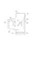
図12(a)は、厚さ1mmの石英基板からなる誘電体基板1201の表面に第一の金属薄膜層1202としてアルミニウムを厚さ30nmで蒸着し、その上に電子線描画(EB)用のレジスト1203を塗布により形成したものである。
In FIG. 12A, aluminum is deposited as a first metal
次に、EB描画装置を用いて、レジスト1203をパターニングする。レジストパターンの形状は、一辺が約120nmの正方形であり、周期約400nmで正方格子状に配列した形状を作製する。このレジストパターンをエッチングマスクとして、塩素と酸素の混合気体のプラズマでドライエッチングすることで第一の金属薄膜構造体1204を作製する。
Next, the resist 1203 is patterned using an EB drawing apparatus. The resist pattern has a square shape with a side of about 120 nm and is arranged in a square lattice pattern with a period of about 400 nm. Using this resist pattern as an etching mask, the first metal
次に、第一の金属薄膜構造体1204の上に、第一の誘電体層1205として厚さ300nmの石英薄膜をスパッタリングにより形成する。第一の誘電体層1205の厚さは300nmに限るものではないが、次の工程で作製する第二の金属薄膜構造体層と近接場相互作用を及ぼしあわない層間距離を確保することが好ましい。
Next, a quartz thin film having a thickness of 300 nm is formed as a
次に、図12(b)に示すように、第一の誘電体層1205の表面に、第二の金属薄膜層1206としてアルミニウムを厚さ30nmで蒸着する。そして、この第二の金属薄膜層1206の上にレジスト層として電子線描画(EB)用レジストを塗布する。そして、EB描画装置にてレジスト層をパターニングする。レジストパターンの形状は、一辺が約70nmの正方形であり、周期約250nmで正方格子状に配列した形状を作製する。このレジストパターンをエッチングマスクとして、塩素と酸素の混合気体のプラズマでドライエッチングすることで第二の金属薄膜構造体1207を作製する。
Next, as shown in FIG. 12B, aluminum is deposited as a second metal
次に、図12(c)に示すように、第二の金属構造体1207の上に、第二の誘電体層1208として厚さ400nmの石英薄膜をスパッタリングにより形成する。
Next, as shown in FIG. 12C, a quartz thin film having a thickness of 400 nm is formed as a
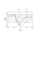
図13には、このようにして作製した積層型の光学フィルタの透過スペクトルを示した。このフィルタの第一の金属薄膜構造体の透過スペクトル1301は吸収ピーク波長約650nm付近、第二の金属薄膜構造体の透過スペクトル1302は吸収ピーク波長約450nm付近である。このため、本実施例のフィルタの積層フィルタ透過スペクトル1303はこれらの積の形になる。したがって、本実施例に係る積層型フィルタは緑を透過する光フィルタとして機能することがわかる。つまり、各層単層では補色フィルタとして機能するフィルタを、積層構造としたことで原色フィルタとして機能させることが出来るようになる。
FIG. 13 shows a transmission spectrum of the laminated optical filter thus manufactured. The
実施例4では、大きさの異なる金属構造体が交互に配列することにより、すなわち2つの金属構造体群が重複して配置することにより、複数の透過スペクトルを複合させた透過スペクトルを有するフィルタを単層で実現できる例について説明する。 In the fourth embodiment, a filter having a transmission spectrum in which a plurality of transmission spectra are combined is obtained by alternately arranging metal structures having different sizes, that is, by arranging two metal structure groups in an overlapping manner. An example that can be realized with a single layer will be described.
図15(a)は、一辺が90nmの正方形のアルミニウムからなる金属構造体1501と、一辺が150nmの正方形のアルミニウムからなる金属構造体1502が配列されている例を示したものである。これらの金属構造体の厚さは60nmであり、金属構造体1501と1502は、周期1506で互い違いに正方格子状に配列されている。ここでは周期1506は250nmとしている。
FIG. 15A shows an example in which a
図15(b)には、このようにして作製した光学フィルタの透過スペクトル1503を示した。一方、リファレンスとして、一辺90nmの正方形のアルミニウムを厚さ60nm、周期250nmで正方格子状に配列した光学フィルタの透過スペクトル1504を示した。また、一辺150nmの正方形のアルミニウムを厚さ60nm、周期400nmで正方格子状に配列した光学フィルタの透過スペクトル1505を示した。
FIG. 15B shows a
このように、本実施例に係る光学フィルタは、透過スペクトル1503を有するため、単層構造ながら2層のフィルタが有する両方の特性を発現するスペクトルを得ることができる。
As described above, since the optical filter according to the present example has the
また、透過スペクトル1503は波長600nm付近に透過率最大値を持つフィルタの特性を有すると考えることもでき、補色フィルタ2層分の機能を一層で発現させることが可能となる。なお、本実施例に係る光学フィルタは、単層の金属構造体のフィルタを積層する場合と比較して更に簡易に作製することが可能となる。
In addition, the
本実施例では、面内に2種類の金属構造体の形状が混在する例を挙げたが、面内に存在する金属微粒子形状は3種類以上であってもよく、また周期を変調させた構造体群を配置して所望の光学特性を得るように設計しても良い。 In this embodiment, an example in which the shape of two types of metal structures coexists in the plane has been given, but there may be three or more types of metal fine particles present in the plane, and the structure in which the period is modulated. The body group may be arranged so as to obtain a desired optical characteristic.
本実施例は、実施例1ないし4で説明したいずれかの光学フィルタを用いた光検出素子、および光検出素子をアレイ状に並べて撮像素子を構成し、この撮像素子をデジタルカメラに組み込んだ例である。 This embodiment is an example in which an optical sensor using any one of the optical filters described in the first to fourth embodiments and an optical sensor are arranged in an array to constitute an imaging device, and this imaging device is incorporated in a digital camera. It is.
図23は、本発明の光学フィルタを用いた光検出素子の模式図である。
光検出素子2507は、マイクロレンズ2501を通して外部から入射した光を光電変換部2505に導入する。光電変換部では入射光に応じた電荷を発生させる。光検出素子は光電変換部2505のほかに本発明で開示される光学フィルタ2502、誘電体層2503、電気回路部2504、半導体基板2506を含んでいる。光学フィルタ2502には例えば図1に示す金属構造体120のような、光に対してプラズモン共鳴を誘起し得る構造を含んでいる。
FIG. 23 is a schematic diagram of a photodetecting element using the optical filter of the present invention.
The
図24は、本発明の光学フィルタを用いた撮像素子の模式図である。 FIG. 24 is a schematic diagram of an image sensor using the optical filter of the present invention.
図24において、画素エリア2600は、前述の複数の光検出素子(画素)2601a〜2603cを、3行×3列の2次元マトリクス状に配置している。尚、図24では、画素エリア2600は、3行×3列の2次元マトリクス状としたが、例えば、7680×4320列のマトリクスとすることも可能である。
In FIG. 24, the
図24において、垂直走査回路2605および水平走査回路2604は、画素エリア2600内に配置されている光検出素子(画素)を選択して読み出すための回路である。
In FIG. 24, a
図24のように構成した撮像素子をデジタルカメラに組み込んだ模式図を図25に示す。 FIG. 25 shows a schematic diagram in which an image sensor configured as shown in FIG. 24 is incorporated in a digital camera.
図25において、2701はカメラ本体、2709は接眼レンズ、2711はシャッターであり、2716は、ミラーである。
In FIG. 25,
本発明に係る撮像素子は2706であり、レンズ鏡筒2705内に配された撮影光学系(レンズ)2702を介し、撮像素子2706に光が入射する。これにより被写体像に応じて、撮像素子2706の各画素に電荷が発生し、発生した電荷に対応して被写体像を再現できる。被写体像は、モニター用ディスプレイ装置2707で再生できる他、メモリーカード等の記録媒体2708に記録される。
The image pickup device according to the present invention is 2706, and light enters the
本発明に係る光学フィルタは、一般的な色素で構成されるカラーフィルタと比較して厚みが薄いため、ここで示した本発明の撮像素子を薄く構成できる。その結果、撮像素子表面から撮像素子光電変換部までの距離が短くなるため、光の利用効率が向上する。これにより、本発明に係る撮像素子の感度向上が可能である。 Since the optical filter according to the present invention is thinner than a color filter composed of a general pigment, the imaging device of the present invention shown here can be configured thinly. As a result, since the distance from the image sensor surface to the image sensor photoelectric conversion unit is shortened, the light use efficiency is improved. Thereby, the sensitivity of the image sensor according to the present invention can be improved.
110 誘電体基板
120 金属構造体
121 第1の金属構造体
122 第1の金属構造体
130 誘電体層
140 第一の方向
141 第一の長さ
145 周期
150 第二の方向
151 第二の長さ
155 周期
160 金属構造体の厚さ
170 誘電体層の厚さから金属構造体の厚さを減じた厚さ
201 透過スペクトルR
202 透過スペクトルG
203 透過スペクトルB
301 領域
302 領域
303 領域
401 第1の金属構造体
402 第1の金属構造体群
403 第1の金属構造体
404 第1の金属構造体群
405 周期
406 周期
407 第1の金属構造体
408 第2の金属構造体
501 第1の金属構造体群
502 第1の方向
503 第2の方向
504 第1の長さ
505 第2の長さ
506 第2の金属構造体群
507 第3の長さ
508 第4の長さ
701 誘電体基板
702 第1の金属構造体群
703 第1の誘電体層
704 第3の金属構造体群
705 第2の誘電体層(他の誘電体層)
801 誘電体基板
802 金属薄膜層
803 レジスト
804 金属薄膜構造体
805 誘電体層
901 透過スペクトルR
902 透過スペクトルG
903 透過スペクトルB
904 反射スペクトルR
905 反射スペクトルG
906 反射スペクトルB
1001 誘電体基板
1002 金属薄膜層
1003 電子線描画用レジスト
1004 パターン部A
1005 パターン部B
1006 パターン部C
1007 金属薄膜構造体
1008 誘電体層
1101 透過スペクトルR
1102 透過スペクトルG
1103 透過スペクトルB
1201 誘電体基板
1202 第一の金属薄膜層
1203 レジスト
1204 第一の金属薄膜構造体
1205 第一の誘電体層
1206 第二の金属薄膜層
1207 第二の金属薄膜層
1208 第二の誘電体層
1301 透過スペクトル
1302 透過スペクトル
1303 積層フィルタ透過スペクトル
1401 誘電体基板
1402 金属
1403 金属上面
1404 金属下面
1501 金属構造体
1502 金属構造体
1503 透過スペクトル
1504 透過スペクトル
1505 透過スペクトル
1506 周期
1601 第1の金属構造体
1602 第1の金属構造体群
1603 第2の金属構造体
1604 第2の金属構造体群
1801 第1の長さ
1802 第2の長さ
2201 透過スペクトル
2202 透過スペクトル
DESCRIPTION OF
202 Transmission spectrum G
203 Transmission spectrum B
301
801
902 Transmission spectrum G
903 Transmission spectrum B
904 Reflection spectrum R
905 reflection spectrum G
906 Reflection spectrum B
1001
1005 Pattern part B
1006 Pattern part C
1007 Metal
1102 Transmission spectrum G
1103 Transmission spectrum B
1201
Claims (16)
誘電体基板と、
前記誘電体基板の表面上に、複数の第1の金属構造体を面内方向に孤立した状態で2次元的に設けた第1の金属構造体群と、
前記第1の金属構造体群を覆う誘電体層と、を有し、
前記第1の金属構造体は、第1の方向に第1の長さを有し、かつ、第1の方向と直交する第2の方向に第2の長さを有し、該第1の長さと該第2の長さは、前記第1の波長以下の長さであり、
前記第1の金属構造体と、前記誘電体基板または前記誘電体層に入射する光とが共鳴することにより前記第1の金属構造体の表面に誘起される局在プラズモンによって、前記第1の波長の透過率を極小値または反射率を極大値とさせると共に、
前記第1の長さおよび第2の長さが110nm以上160nm以下の範囲であり、かつ前記第1の金属構造体の厚さが10nm以上100nm以下の範囲であり、かつ前記第1の金属構造体が設けられている周期が340nm以上450nm以下の範囲であり、前記第1の波長が550nm以上から650nm未満の範囲にあることを特徴とする光学フィルタ。 An optical filter that transmits or reflects light of a first wavelength,
A dielectric substrate;
A first metal structure group in which a plurality of first metal structures are two-dimensionally provided on the surface of the dielectric substrate in a state of being isolated in an in-plane direction;
A dielectric layer covering the first metal structure group,
The first metal structure has a first length in a first direction and a second length in a second direction orthogonal to the first direction. The length and the second length are less than or equal to the first wavelength,
The first metal structure and the light incident on the dielectric substrate or the dielectric layer resonate with each other, and the first plasmon is induced by the localized plasmon induced on the surface of the first metal structure. While setting the wavelength transmittance to the minimum value or the reflectance to the maximum value ,
The first length and the second length are in the range of 110 nm to 160 nm, and the thickness of the first metal structure is in the range of 10 nm to 100 nm, and the first metal structure An optical filter , wherein a period in which a body is provided is in a range of 340 nm to 450 nm, and the first wavelength is in a range of 550 nm to less than 650 nm .
誘電体基板と、
前記誘電体基板の表面上に、複数の第1の金属構造体を面内方向に孤立した状態で2次元的に設けた第1の金属構造体群と、
前記第1の金属構造体群を覆う誘電体層と、を有し、
前記第1の金属構造体は、第1の方向に第1の長さを有し、かつ、第1の方向と直交する第2の方向に第2の長さを有し、該第1の長さと該第2の長さは、前記第1の波長以下の長さであり、
前記第1の金属構造体と、前記誘電体基板または前記誘電体層に入射する光とが共鳴することにより前記第1の金属構造体の表面に誘起される局在プラズモンによって、前記第1の波長の透過率を極小値または反射率を極大値とさせると共に、
前記第1の長さおよび第2の長さが90nm以上130nm未満の範囲であり、かつ前記第1の金属構造体の厚さが10nm以上100nm以下の範囲であり、かつ前記第1の金属構造体が設けられている周期が260nm以上340nm以下の範囲であり、前記第1の波長が450nm以上から550nm未満の範囲にあることを特徴とする光学フィルタ。 An optical filter that transmits or reflects light of a first wavelength,
A dielectric substrate;
A first metal structure group in which a plurality of first metal structures are two-dimensionally provided on the surface of the dielectric substrate in a state of being isolated in an in-plane direction;
A dielectric layer covering the first metal structure group,
The first metal structure has a first length in a first direction and a second length in a second direction orthogonal to the first direction. The length and the second length are less than or equal to the first wavelength,
The first metal structure and the light incident on the dielectric substrate or the dielectric layer resonate with each other, and the first plasmon is induced by the localized plasmon induced on the surface of the first metal structure. While setting the wavelength transmittance to the minimum value or the reflectance to the maximum value,
The first length and the second length are in the range of 90 nm to less than 130 nm, and the thickness of the first metal structure is in the range of 10 nm to 100 nm, and the first metal structure An optical filter , wherein a period in which a body is provided is in a range of 260 nm to 340 nm, and the first wavelength is in a range of 450 nm to less than 550 nm .
誘電体基板と、
前記誘電体基板の表面上に、複数の第1の金属構造体を面内方向に孤立した状態で2次元的に設けた第1の金属構造体群と、
前記第1の金属構造体群を覆う誘電体層と、を有し、
前記第1の金属構造体は、第1の方向に第1の長さを有し、かつ、第1の方向と直交する第2の方向に第2の長さを有し、該第1の長さと該第2の長さは、前記第1の波長以下の長さであり、
前記第1の金属構造体と、前記誘電体基板または前記誘電体層に入射する光とが共鳴することにより前記第1の金属構造体の表面に誘起される局在プラズモンによって、前記第1の波長の透過率を極小値または反射率を極大値とさせると共に、
前記第1の長さおよび第2の長さが60nm以上100nm未満の範囲であり、かつ前記第1の金属構造体の厚さが10nm以上100nm以下の範囲であり、かつ前記第1の金属構造体が設けられている周期が180nm以上280nm以下の範囲であり、前記第1の波長が350nm以上から450nm未満の範囲にあることを特徴とする光学フィルタ。 An optical filter that transmits or reflects light of a first wavelength,
A dielectric substrate;
A first metal structure group in which a plurality of first metal structures are two-dimensionally provided on the surface of the dielectric substrate in a state of being isolated in an in-plane direction;
A dielectric layer covering the first metal structure group,
The first metal structure has a first length in a first direction and a second length in a second direction orthogonal to the first direction. The length and the second length are less than or equal to the first wavelength,
The first metal structure and the light incident on the dielectric substrate or the dielectric layer resonate with each other, and the first plasmon is induced by the localized plasmon induced on the surface of the first metal structure. While setting the wavelength transmittance to the minimum value or the reflectance to the maximum value,
The first length and the second length are in the range of 60 nm to less than 100 nm, and the thickness of the first metal structure is in the range of 10 nm to 100 nm, and the first metal structure An optical filter , wherein a period in which a body is provided is in a range of 180 nm to 280 nm, and the first wavelength is in a range of 350 nm to less than 450 nm .
誘電体基板と、
前記誘電体基板の表面上に、複数の第1の金属構造体を面内方向に孤立した状態で2次元的に設けた第1の金属構造体群と、
前記第1の金属構造体群を覆う誘電体層と、を有し、
前記第1の金属構造体は、第1の方向に第1の長さを有し、かつ、第1の方向と直交する第2の方向に第2の長さを有し、該第1の長さと該第2の長さは、前記第1の波長以下の長さであり、
前記第1の金属構造体と、前記誘電体基板または前記誘電体層に入射する光とが共鳴することにより前記第1の金属構造体の表面に誘起される局在プラズモンによって、前記第1の波長の透過率を極小値または反射率を極大値とさせると共に、
前記第1の金属構造体群とは別に、前記誘電体基板の面内方向に、複数の第2の金属構造体を孤立した状態で2次元的に設けた第2の金属構造体群を有し、
該第2の金属構造体は、前記第1の方向に第3の長さを有し、かつ前記第2の方向に第4の長さを有し、該第3の長さと該第4の長さは前記第1の波長とは異なる第2の波長以下であり、
該第3の長さは前記第1の長さと異なるか、または該第4の長さは前記第2の長さと異なっており、
前記第1の金属構造体群と、前記第2の金属構造体群とは前記誘電体基板表面の相異なる領域に配置され、
前記第2の金属構造体と、前記誘電体基板または前記誘電体層に入射する光とが共鳴することにより前記第2の金属構造体の表面に誘起される局在プラズモンによって、前記第2の波長の透過率を極小値または反射率を極大値とさせることを特徴とする光学フィルタ。 An optical filter that transmits or reflects light of a first wavelength,
A dielectric substrate;
A first metal structure group in which a plurality of first metal structures are two-dimensionally provided on the surface of the dielectric substrate in a state of being isolated in an in-plane direction;
A dielectric layer covering the first metal structure group,
The first metal structure has a first length in a first direction and a second length in a second direction orthogonal to the first direction. The length and the second length are less than or equal to the first wavelength,
The first metal structure and the light incident on the dielectric substrate or the dielectric layer resonate with each other, and the first plasmon is induced by the localized plasmon induced on the surface of the first metal structure. While setting the wavelength transmittance to the minimum value or the reflectance to the maximum value,
Separately from the first metal structure group, there is a second metal structure group in which a plurality of second metal structures are two-dimensionally provided in an in-plane direction of the dielectric substrate. And
The second metal structure has a third length in the first direction and a fourth length in the second direction, and the third length and the fourth length The length is equal to or less than a second wavelength different from the first wavelength;
The third length is different from the first length, or the fourth length is different from the second length;
The first metal structure group and the second metal structure group are arranged in different regions on the surface of the dielectric substrate,
The second metal structure and the second plasmon induced on the surface of the second metal structure by resonance between light incident on the dielectric substrate or the dielectric layer, An optical filter characterized in that the transmittance of wavelength is a minimum value or the reflectance is a maximum value .
誘電体基板と、
前記誘電体基板の表面上に、複数の第1の金属構造体を面内方向に孤立した状態で2次元的に設けた第1の金属構造体群と、
前記第1の金属構造体群を覆う誘電体層と、を有し、
前記第1の金属構造体は、第1の方向に第1の長さを有し、かつ、第1の方向と直交する第2の方向に第2の長さを有し、該第1の長さと該第2の長さは、前記第1の波長以下の長さであり、
前記第1の金属構造体と、前記誘電体基板または前記誘電体層に入射する光とが共鳴することにより前記第1の金属構造体の表面に誘起される局在プラズモンによって、前記第1の波長の透過率を極小値または反射率を極大値とさせると共に、
前記誘電体基板の面内方向に、前記第1の金属構造体群を2つ以上有し、
該2つ以上の前記第1の金属構造体群は重複した領域に配置されていることを特徴とする光学フィルタ。 An optical filter that transmits or reflects light of a first wavelength,
A dielectric substrate;
A first metal structure group in which a plurality of first metal structures are two-dimensionally provided on the surface of the dielectric substrate in a state of being isolated in an in-plane direction;
A dielectric layer covering the first metal structure group,
The first metal structure has a first length in a first direction and a second length in a second direction orthogonal to the first direction. The length and the second length are less than or equal to the first wavelength,
The first metal structure and the light incident on the dielectric substrate or the dielectric layer resonate with each other, and the first plasmon is induced by the localized plasmon induced on the surface of the first metal structure. While setting the wavelength transmittance to the minimum value or the reflectance to the maximum value,
Having two or more of the first metal structures in the in-plane direction of the dielectric substrate;
The optical filter, wherein the two or more first metal structure groups are arranged in an overlapping region .
誘電体基板と、
前記誘電体基板の表面上に、複数の第1の金属構造体を面内方向に孤立した状態で2次元的に設けた第1の金属構造体群と、
前記第1の金属構造体群を覆う誘電体層と、を有し、
前記第1の金属構造体は、第1の方向に第1の長さを有し、かつ、第1の方向と直交する第2の方向に第2の長さを有し、該第1の長さと該第2の長さは、前記第1の波長以下の長さであり、
前記第1の金属構造体と、前記誘電体基板または前記誘電体層に入射する光とが共鳴することにより前記第1の金属構造体の表面に誘起される局在プラズモンによって、前記第1の波長の透過率を極小値または反射率を極大値とさせると共に、
前記誘電体基板の面内方向に、前記第1の金属構造体群を2つ以上有し、
該2つ以上の第1の金属構造体群を構成する前記第1の構造体が設けられている周期は互いに異なっており、
該2つ以上の前記第1の金属構造体群は重複した領域に配置されていることを特徴とする光学フィルタ。 An optical filter that transmits or reflects light of a first wavelength,
A dielectric substrate;
A first metal structure group in which a plurality of first metal structures are two-dimensionally provided on the surface of the dielectric substrate in a state of being isolated in an in-plane direction;
A dielectric layer covering the first metal structure group,
The first metal structure has a first length in a first direction and a second length in a second direction orthogonal to the first direction. The length and the second length are less than or equal to the first wavelength,
The first metal structure and the light incident on the dielectric substrate or the dielectric layer resonate with each other, and the first plasmon is induced by the localized plasmon induced on the surface of the first metal structure. While setting the wavelength transmittance to the minimum value or the reflectance to the maximum value,
Having two or more of the first metal structures in the in-plane direction of the dielectric substrate;
The periods in which the first structures constituting the two or more first metal structure groups are provided are different from each other,
The optical filter, wherein the two or more first metal structure groups are arranged in an overlapping region .
誘電体基板と、
前記誘電体基板の表面上に、複数の第1の金属構造体を面内方向に孤立した状態で2次元的に設けた第1の金属構造体群と、
前記第1の金属構造体群を覆う誘電体層と、を有し、
前記第1の金属構造体は、第1の方向に第1の長さを有し、かつ、第1の方向と直交する第2の方向に第2の長さを有し、該第1の長さと該第2の長さは、前記第1の波長以下の長さであり、
前記第1の金属構造体と、前記誘電体基板または前記誘電体層に入射する光とが共鳴することにより前記第1の金属構造体の表面に誘起される局在プラズモンによって、前記第1の波長の透過率を極小値または反射率を極大値とさせると共に、
前記第1の金属構造体群とは別に、前記誘電体基板の面内方向に、複数の第2の金属構造体を孤立した状態で2次元的に設けた第2の金属構造体群を有し、
該第2の金属構造体は、前記第1の方向に第3の長さを有し、かつ前記第2の方向に第4の長さを有し、該第3の長さと該第4の長さは前記第1の波長とは異なる第2の波長以下であり、
該第3の長さは前記第1の長さと異なるか、または該第4の長さは前記第2の長さと異なっており、
前記第1の金属構造体群と、前記第2の金属構造体群とは重複した領域に配置され、
前記第2の金属構造体と、前記誘電体基板または前記誘電体層に入射する光とが共鳴することにより前記第2の金属構造体の表面に誘起される局在プラズモンによって、前記第2の波長の透過率を極小値または反射率を極大値とさせることを特徴とする光学フィルタ。 An optical filter that transmits or reflects light of a first wavelength,
A dielectric substrate;
A first metal structure group in which a plurality of first metal structures are two-dimensionally provided on the surface of the dielectric substrate in a state of being isolated in an in-plane direction;
A dielectric layer covering the first metal structure group,
The first metal structure has a first length in a first direction and a second length in a second direction orthogonal to the first direction. The length and the second length are less than or equal to the first wavelength,
The first metal structure and the light incident on the dielectric substrate or the dielectric layer resonate with each other, and the first plasmon is induced by the localized plasmon induced on the surface of the first metal structure. While setting the wavelength transmittance to the minimum value or the reflectance to the maximum value,
Separately from the first metal structure group, there is a second metal structure group in which a plurality of second metal structures are two-dimensionally provided in an in-plane direction of the dielectric substrate. And
The second metal structure has a third length in the first direction and a fourth length in the second direction, and the third length and the fourth length The length is equal to or less than a second wavelength different from the first wavelength;
The third length is different from the first length, or the fourth length is different from the second length;
The first metal structure group and the second metal structure group are arranged in an overlapping region,
The second metal structure and the second plasmon induced on the surface of the second metal structure by resonance between light incident on the dielectric substrate or the dielectric layer, An optical filter characterized in that the transmittance of wavelength is a minimum value or the reflectance is a maximum value .
誘電体基板と、
前記誘電体基板の表面上に、複数の第1の金属構造体を面内方向に孤立した状態で2次元的に設けた第1の金属構造体群と、
前記第1の金属構造体群を覆う誘電体層と、を有し、
前記第1の金属構造体は、第1の方向に第1の長さを有し、かつ、第1の方向と直交する第2の方向に第2の長さを有し、該第1の長さと該第2の長さは、前記第1の波長以下の長さであると共に、
前記誘電体層の表面の上に、更に他の誘電体層が形成されており、
前記誘電体層の表面と前記他の誘電体層との間に、複数の第2の金属構造体を前記誘電体層の表面の面内方向に孤立した状態で2次元的に設けた第2の金属構造体群を有し、
該第2の金属構造体群を構成する第2の金属構造体は、前記第1の方向に第3の長さを有し、かつ前記第2の方向に第4の長さを有し、該第3の長さと該第4の長さは、前記第1の波長とは異なる第2の波長以下の長さであり、
前記第1の長さと前記第3の長さが異なるか若しくは前記第2の長さと前記第4の長さが異なるか、又は、第2の金属構造体が設けられている周期と第1の金属構造体が設けられている周期とが異なり、
第1の金属構造体の表面に誘起される局在プラズモンにより、第1の波長の透過率を極小値または反射率を極大値とさせ、かつ、
第2の金属構造体の表面に誘起される局在プラズモンにより、前記第2の波長の透過率を極小値または反射率を極大値とさせることを特徴とする積層型の光学フィルタ。 An optical filter in which an optical filter that transmits or reflects light of a first wavelength and an optical filter that transmits or reflects light of a second wavelength are stacked,
A dielectric substrate;
A first metal structure group in which a plurality of first metal structures are two-dimensionally provided on the surface of the dielectric substrate in a state of being isolated in an in-plane direction;
A dielectric layer covering the first metal structure group,
The first metal structure has a first length in a first direction and a second length in a second direction orthogonal to the first direction. The length and the second length are not more than the first wavelength, and
Another dielectric layer is formed on the surface of the dielectric layer,
A plurality of second metal structures two-dimensionally provided between the surface of the dielectric layer and the other dielectric layer so as to be isolated in the in-plane direction of the surface of the dielectric layer; A metal structure group of
A second metal structure constituting the second metal structure group has a third length in the first direction and a fourth length in the second direction; The third length and the fourth length are not more than a second wavelength different from the first wavelength, and
The first length is different from the third length, or the second length is different from the fourth length, or the period in which the second metal structure is provided and the first length Unlike the period in which the metal structure is provided,
The local plasmon induced on the surface of the first metal structure causes the transmittance of the first wavelength to be a minimum value or the reflectance to be a maximum value; and
A laminated optical filter characterized in that the transmittance of the second wavelength is minimized or the reflectance is maximized by localized plasmons induced on the surface of the second metal structure .
Priority Applications (1)
| Application Number | Priority Date | Filing Date | Title |
|---|---|---|---|
| JP2008181500A JP4621270B2 (en) | 2007-07-13 | 2008-07-11 | Optical filter |
Applications Claiming Priority (3)
| Application Number | Priority Date | Filing Date | Title |
|---|---|---|---|
| JP2007184599 | 2007-07-13 | ||
| JP2008136686 | 2008-05-26 | ||
| JP2008181500A JP4621270B2 (en) | 2007-07-13 | 2008-07-11 | Optical filter |
Publications (3)
| Publication Number | Publication Date |
|---|---|
| JP2010008990A JP2010008990A (en) | 2010-01-14 |
| JP2010008990A5 JP2010008990A5 (en) | 2010-07-15 |
| JP4621270B2 true JP4621270B2 (en) | 2011-01-26 |
Family
ID=39869925
Family Applications (1)
| Application Number | Title | Priority Date | Filing Date |
|---|---|---|---|
| JP2008181500A Active JP4621270B2 (en) | 2007-07-13 | 2008-07-11 | Optical filter |
Country Status (5)
| Country | Link |
|---|---|
| US (2) | US8094394B2 (en) |
| JP (1) | JP4621270B2 (en) |
| KR (1) | KR101175455B1 (en) |
| CN (1) | CN101730857B (en) |
| WO (1) | WO2009011439A1 (en) |
Families Citing this family (108)
| Publication number | Priority date | Publication date | Assignee | Title |
|---|---|---|---|---|
| JP4621270B2 (en) * | 2007-07-13 | 2011-01-26 | キヤノン株式会社 | Optical filter |
| JP4995231B2 (en) | 2008-05-30 | 2012-08-08 | キヤノン株式会社 | Optical filter |
| US9081251B2 (en) * | 2008-07-31 | 2015-07-14 | Nxp B.V. | Display device |
| JP5538813B2 (en) * | 2008-12-26 | 2014-07-02 | キヤノン株式会社 | Optical element, and image sensor and imaging apparatus using the same |
| WO2010134063A2 (en) * | 2009-05-18 | 2010-11-25 | Mendlovic, David | Image sensor and method of producing the same |
| KR101048768B1 (en) * | 2009-06-10 | 2011-07-15 | (주)실리콘화일 | Image sensor for measuring illuminance, proximity and color temperature |
| JP4880093B2 (en) * | 2009-06-11 | 2012-02-22 | パイオニア株式会社 | Light emitting element and display device |
| NL2005118A (en) * | 2009-08-21 | 2011-02-22 | Asml Netherlands Bv | Spectral purity filters for use in a lithographic apparatus. |
| NL2005111A (en) * | 2009-08-21 | 2011-02-22 | Asml Netherlands Bv | Spectral purity filters for use in a lithographic apparatus. |
| JP2011043681A (en) * | 2009-08-21 | 2011-03-03 | Canon Inc | Optical apparatus, optical detector, optical modulator, imaging apparatus, and camera |
| JP4743917B2 (en) * | 2009-08-25 | 2011-08-10 | Necシステムテクノロジー株式会社 | Optical unit |
| KR101338117B1 (en) * | 2009-10-29 | 2013-12-06 | 엘지디스플레이 주식회사 | Liquid crystal display device and method of fabricating the same |
| KR101274591B1 (en) * | 2009-12-18 | 2013-06-13 | 엘지디스플레이 주식회사 | Color filter using surface plasmon and liquid crystal display device, and method of fabricating the same |
| JP2011138950A (en) * | 2009-12-28 | 2011-07-14 | Sony Corp | Semiconductor device, and electronic apparatus |
| JP2011159858A (en) * | 2010-02-02 | 2011-08-18 | Sony Corp | Solid-state imaging device and method of manufacturing the same, and electronic apparatus |
| JP4812141B2 (en) * | 2010-03-24 | 2011-11-09 | Necシステムテクノロジー株式会社 | Analysis equipment |
| US8770749B2 (en) | 2010-04-15 | 2014-07-08 | Oakley, Inc. | Eyewear with chroma enhancement |
| KR20130118729A (en) * | 2010-04-27 | 2013-10-30 | 더 리젠츠 오브 더 유니버시티 오브 미시건 | Display device having plasmonic color filters and photovoltaic capabilities |
| JP5645513B2 (en) * | 2010-07-07 | 2014-12-24 | キヤノン株式会社 | Solid-state imaging device and imaging system |
| KR101455545B1 (en) | 2010-07-15 | 2014-10-27 | 프라운호퍼 게젤샤프트 쭈르 푀르데룽 데어 안겐반텐 포르슝 에. 베. | Optical bandpass filter system, in particular for multichannel spectral-selective measurements |
| JP5500007B2 (en) * | 2010-09-03 | 2014-05-21 | ソニー株式会社 | Solid-state imaging device and camera system |
| JP2012059865A (en) * | 2010-09-08 | 2012-03-22 | Sony Corp | Imaging element and imaging device |
| JP2012064703A (en) * | 2010-09-15 | 2012-03-29 | Sony Corp | Image sensor and image pick-up device |
| JP5270738B2 (en) * | 2011-04-12 | 2013-08-21 | シャープ株式会社 | Optical filter, display cell and display device |
| CN103547948A (en) | 2011-04-20 | 2014-01-29 | 密执安州立大学董事会 | Spectrum filtering for visual displays and imaging having minimal angle dependence |
| EP2521179B1 (en) * | 2011-05-06 | 2015-10-07 | ELMOS Semiconductor AG | Device for recording the spectrum of electromagnetic radiation within a pre-defined wavelength range |
| JP5821511B2 (en) * | 2011-10-17 | 2015-11-24 | セイコーエプソン株式会社 | Optical device and detection apparatus |
| EP2769262A4 (en) | 2011-10-20 | 2015-04-01 | Oakley Inc | Eyewear with chroma enhancement |
| US20130153861A1 (en) * | 2011-12-16 | 2013-06-20 | Bozena Kaminska | Organic optoelectronic devices with surface plasmon structures and methods of manufacture |
| JP5867810B2 (en) * | 2011-12-20 | 2016-02-24 | 国立研究開発法人物質・材料研究機構 | Vertically stacked plasmon metal disk array for capturing broadband light |
| JP2013179297A (en) * | 2012-02-10 | 2013-09-09 | Tokyo Institute Of Technology | Solar cell having optical control layer |
| CN102540304A (en) * | 2012-03-08 | 2012-07-04 | 电子科技大学 | Two-dimensional periodic hole-type Talbot medium phase grating |
| WO2013169987A1 (en) | 2012-05-10 | 2013-11-14 | Oakley, Inc. | Eyewear with laminated functional layers |
| JP5943764B2 (en) * | 2012-08-02 | 2016-07-05 | 三菱電機株式会社 | Electromagnetic wave sensor and electromagnetic wave sensor device |
| JP5907011B2 (en) | 2012-09-07 | 2016-04-20 | 株式会社デンソー | Optical sensor |
| FR3000227B1 (en) * | 2012-12-20 | 2018-01-19 | Commissariat A L'energie Atomique Et Aux Energies Alternatives | OPTICAL FILTER AND DETECTOR COMPRISING SUCH A FILTER |
| US9627434B2 (en) * | 2013-01-04 | 2017-04-18 | California Institute Of Technology | System and method for color imaging with integrated plasmonic color filters |
| JP6033121B2 (en) * | 2013-02-27 | 2016-11-30 | 三菱電機株式会社 | Wavelength conversion element |
| US9547107B2 (en) | 2013-03-15 | 2017-01-17 | The Regents Of The University Of Michigan | Dye and pigment-free structural colors and angle-insensitive spectrum filters |
| JP6217120B2 (en) * | 2013-04-19 | 2017-10-25 | 三菱電機株式会社 | Wavelength conversion element and wavelength conversion device |
| JP6105728B2 (en) * | 2013-06-14 | 2017-03-29 | シャープ株式会社 | Solid-state imaging device |
| JP6226606B2 (en) * | 2013-07-23 | 2017-11-08 | キヤノン株式会社 | Color filter array, solid-state imaging device, imaging device |
| JP6126490B2 (en) * | 2013-08-05 | 2017-05-10 | シャープ株式会社 | Optical filter |
| JP6381645B2 (en) * | 2013-08-06 | 2018-08-29 | コーニンクレッカ フィリップス エヌ ヴェKoninklijke Philips N.V. | Lighting device |
| WO2015025637A1 (en) * | 2013-08-23 | 2015-02-26 | シャープ株式会社 | Photoelectric conversion device and method for manufacturing same |
| WO2015033611A1 (en) * | 2013-09-04 | 2015-03-12 | シャープ株式会社 | Optical filter and imaging element |
| JP6211485B2 (en) * | 2013-12-03 | 2017-10-11 | 富士フイルム株式会社 | Anti-reflective optical member |
| JP6193754B2 (en) * | 2013-12-20 | 2017-09-06 | 三菱電機株式会社 | Electromagnetic wave detector |
| US9575335B1 (en) | 2014-01-10 | 2017-02-21 | Oakley, Inc. | Eyewear with chroma enhancement for specific activities |
| JP2015176768A (en) * | 2014-03-14 | 2015-10-05 | スタンレー電気株式会社 | Filament, polarized radiation light source device, polarized infrared radiation heater and manufacturing method of filament |
| CN103915520A (en) * | 2014-04-14 | 2014-07-09 | 上海电机学院 | Silicon-based thin film solar cell with surface provided with metal grid structure |
| KR102219705B1 (en) * | 2014-05-09 | 2021-02-24 | 삼성전자주식회사 | Spectro-sensor and spectrometer employing the spectro-sensor |
| EP2942618B1 (en) * | 2014-05-09 | 2017-07-12 | Samsung Electronics Co., Ltd | Spectro-sensor and spectrometer employing the same |
| US10871661B2 (en) | 2014-05-23 | 2020-12-22 | Oakley, Inc. | Eyewear and lenses with multiple molded lens components |
| JP6378767B2 (en) * | 2014-07-15 | 2018-08-22 | シャープ株式会社 | Imaging device and analysis device |
| GB2528682A (en) * | 2014-07-28 | 2016-02-03 | Isis Innovation | Plasmonic filter |
| JP6537245B2 (en) * | 2014-10-16 | 2019-07-03 | キヤノン株式会社 | Optical element and optical apparatus |
| EP3218763A4 (en) | 2014-11-13 | 2018-06-13 | Oakley, Inc. | Variable light attenuation eyewear with color enhancement |
| US10050075B2 (en) | 2014-11-21 | 2018-08-14 | Lumilant, Inc. | Multi-layer extraordinary optical transmission filter systems, devices, and methods |
| JP2016114627A (en) * | 2014-12-11 | 2016-06-23 | シャープ株式会社 | Optical filter |
| US9905022B1 (en) | 2015-01-16 | 2018-02-27 | Oakley, Inc. | Electronic display for demonstrating eyewear functionality |
| CN104808072A (en) * | 2015-04-29 | 2015-07-29 | 京东方科技集团股份有限公司 | Film structure, testing method thereof, display substrate and testing method and production method thereof |
| US9524416B1 (en) * | 2015-07-03 | 2016-12-20 | Fingerprint Cards Ab | Fingerprint sensing device comprising three-dimensional pattern |
| DE102015010191A1 (en) * | 2015-08-06 | 2017-02-09 | Giesecke & Devrient Gmbh | Security element with subwavelength grid |
| WO2017052196A1 (en) * | 2015-09-21 | 2017-03-30 | 한국과학기술원 | Wideband ultra-high refractivity mesoscopic crystal structure using space-filling of electric dipole and optical device using same |
| US10162091B1 (en) | 2015-10-16 | 2018-12-25 | Board Of Trustees Of The University Of Alabama, For And On Behalf Of The University Of Alabama In Huntsville | Silicon film optical filtering systems and methods of fabrication |
| KR101810573B1 (en) * | 2015-12-16 | 2017-12-19 | 한국과학기술원 | Color filter |
| WO2017135430A1 (en) * | 2016-02-03 | 2017-08-10 | 国立大学法人大阪大学 | Plasmonic structure, color generation structure, and recording medium |
| CN105629364B (en) * | 2016-03-31 | 2018-11-30 | 中国科学院光电技术研究所 | A kind of super surface device of wavelength selective |
| US9749044B1 (en) * | 2016-04-05 | 2017-08-29 | Facebook, Inc. | Luminescent detector for free-space optical communication |
| US9645291B1 (en) * | 2016-04-18 | 2017-05-09 | Ii-Vi Incorporated | Voltage-tunable optical filters for instrumentation applications |
| CN106094087B (en) * | 2016-08-02 | 2019-07-23 | 中国科学院微电子研究所 | A kind of single diffraction order grating |
| KR102294845B1 (en) | 2016-08-02 | 2021-08-30 | 삼성전자주식회사 | Optical Filter, Optical device, and Method for manufacturing optical filter |
| KR102320479B1 (en) * | 2016-08-22 | 2021-11-03 | 삼성전자주식회사 | Spectrometer and Method for Measuring spectrum using the same |
| KR101841131B1 (en) * | 2016-08-22 | 2018-03-22 | 삼성전자주식회사 | Optical Filter, and Optical device using the same |
| KR102020956B1 (en) * | 2016-08-30 | 2019-10-18 | 삼성전자주식회사 | Optical Filter and Optical device Using the Same |
| JP6789792B2 (en) * | 2016-12-13 | 2020-11-25 | ソニーセミコンダクタソリューションズ株式会社 | Image sensor, electronic equipment |
| JP6910704B2 (en) | 2016-12-13 | 2021-07-28 | ソニーセミコンダクタソリューションズ株式会社 | Image sensor, manufacturing method of image sensor, plasmon filter, and electronic equipment |
| JP6338747B2 (en) * | 2017-07-10 | 2018-06-06 | 三菱電機株式会社 | Electromagnetic wave detector |
| JP6232161B1 (en) | 2017-07-27 | 2017-11-15 | 日本板硝子株式会社 | Optical filter |
| JP6267823B1 (en) * | 2017-07-27 | 2018-01-24 | 日本板硝子株式会社 | Optical filter, camera module, and information terminal |
| US11016227B2 (en) | 2017-09-18 | 2021-05-25 | Lumentum Operations Llc | Diffractive optical element |
| CN109599030B (en) * | 2017-09-30 | 2020-12-11 | 昆山国显光电有限公司 | Display screen and electronic product |
| US10381397B2 (en) * | 2017-11-14 | 2019-08-13 | Black Sesame International Holding Limited | Nano metallic planar apex optical detector |
| US10677972B2 (en) * | 2017-12-08 | 2020-06-09 | Viavi Solutions Inc. | Multispectral sensor response balancing |
| US11112622B2 (en) | 2018-02-01 | 2021-09-07 | Luxottica S.R.L. | Eyewear and lenses with multiple molded lens components |
| KR102047425B1 (en) * | 2018-02-20 | 2019-11-21 | 한국과학기술원 | Color filter |
| JP7031446B2 (en) * | 2018-03-30 | 2022-03-08 | 大日本印刷株式会社 | Organic electroluminescence display device |
| CN112020770A (en) * | 2018-04-16 | 2020-12-01 | 应用材料公司 | Multilayer stacked optical element using temporary and permanent bonding |
| JP6981496B2 (en) * | 2018-04-17 | 2021-12-15 | 日本電信電話株式会社 | Color image sensor and image sensor |
| EP3617757B1 (en) * | 2018-08-27 | 2021-02-24 | CSEM Centre Suisse d'Electronique et de Microtechnique SA - Recherche et Développement | Optical filter, optical filter system, spectrometer and method of fabrication thereof |
| JP7255995B2 (en) * | 2018-10-19 | 2023-04-11 | キヤノン電子株式会社 | Optical filter and imaging device |
| KR20200074662A (en) | 2018-12-17 | 2020-06-25 | 삼성전자주식회사 | Phase shift device including metal-dielectric hybrid structure |
| CN109581552A (en) * | 2018-12-27 | 2019-04-05 | 西南技术物理研究所 | It is a kind of for widening the film metal structure of infrared enhancing transmission spectrum |
| CN109932765A (en) * | 2019-02-28 | 2019-06-25 | 湖北大学 | A kind of light absorber and preparation method thereof based on two-dimensional grating |
| WO2020179282A1 (en) * | 2019-03-06 | 2020-09-10 | パナソニックIpマネジメント株式会社 | Light detection device, light detection system, and filter array |
| CN112054308A (en) | 2019-06-05 | 2020-12-08 | 广州方邦电子股份有限公司 | Electromagnetic scattering film and electronic device comprising same |
| JP7400246B2 (en) | 2019-07-30 | 2023-12-19 | セイコーエプソン株式会社 | Wavelength conversion elements, light source devices, and display devices |
| KR102285312B1 (en) * | 2019-08-29 | 2021-08-03 | 이화여자대학교 산학협력단 | Reflective color pixels based on lossy metal |
| KR102255868B1 (en) * | 2019-09-10 | 2021-05-25 | 주식회사 알엠케이 | Optical Filter for color vision deficiency correction and Lens with Optical Filter for color vision deficiency correction |
| KR102389516B1 (en) | 2019-10-18 | 2022-04-21 | 성균관대학교산학협력단 | Photodetector and its manufacturing method |
| KR20210046989A (en) * | 2019-10-21 | 2021-04-29 | 삼성전자주식회사 | Image sensor and image sensing method with improved sensitivity |
| CN110931519A (en) * | 2019-11-18 | 2020-03-27 | 江苏集萃智能传感技术研究所有限公司 | Composite filtering structure for multispectral image sensor |
| EP4052074A4 (en) * | 2019-11-21 | 2022-11-16 | Huawei Technologies Co., Ltd. | Wavelength selective filter and method for fabricating wavelength selective filter |
| CN112436287B (en) * | 2020-11-30 | 2022-07-29 | 江西师范大学 | Electromagnetic super surface, preparation method thereof and nano broadband notch filter |
| CN113078265B (en) * | 2021-03-26 | 2023-04-07 | 联合微电子中心有限责任公司 | CMOS image sensor and manufacturing method thereof |
| JP2023024079A (en) * | 2021-08-06 | 2023-02-16 | ソニーグループ株式会社 | Solid-state imaging device |
| US20230170361A1 (en) * | 2021-11-30 | 2023-06-01 | Visera Technologies Company Ltd. | Optical device |
Citations (1)
| Publication number | Priority date | Publication date | Assignee | Title |
|---|---|---|---|---|
| JP2001133618A (en) * | 1999-11-05 | 2001-05-18 | Nec Corp | Optical transmission equipment |
Family Cites Families (16)
| Publication number | Priority date | Publication date | Assignee | Title |
|---|---|---|---|---|
| SE468188B (en) * | 1991-04-08 | 1992-11-16 | Stiftelsen Inst Foer Mikroelek | METHOD FOR CONNECTING RADIATION IN AN INFRARED DETECTOR, APPLIED DEVICE |
| US5973316A (en) * | 1997-07-08 | 1999-10-26 | Nec Research Institute, Inc. | Sub-wavelength aperture arrays with enhanced light transmission |
| US6236033B1 (en) * | 1998-12-09 | 2001-05-22 | Nec Research Institute, Inc. | Enhanced optical transmission apparatus utilizing metal films having apertures and periodic surface topography |
| AU2001281743A1 (en) | 2000-07-21 | 2002-02-05 | Micro Managed Photons A/S | Surface plasmon polariton band gap structures |
| US7142296B2 (en) * | 2000-10-30 | 2006-11-28 | Sru Biosystems, Inc. | Method and apparatus for detecting biomolecular interactions |
| WO2003019245A2 (en) | 2001-08-31 | 2003-03-06 | Universite Louis Pasteur | Optical transmission apparatus with directionality and divergence control |
| US7248297B2 (en) * | 2001-11-30 | 2007-07-24 | The Board Of Trustees Of The Leland Stanford Junior University | Integrated color pixel (ICP) |
| EP1416303B8 (en) * | 2002-10-30 | 2010-10-13 | Hitachi, Ltd. | Method for manufacturing functional substrates comprising columnar micro-pillars |
| EP1661182A4 (en) | 2003-08-06 | 2011-03-23 | Univ Pittsburgh | Surface plasmon-enhanced nano-optic devices and methods of making same |
| JP2005181979A (en) * | 2003-11-28 | 2005-07-07 | Nippon Sheet Glass Co Ltd | Multilayer structure and its manufacturing method |
| JP2009515203A (en) | 2005-05-18 | 2009-04-09 | ホッブズ,ダグラス,エス. | Microstructured optical device for polarization and wavelength filter processing |
| US20090310133A1 (en) * | 2006-02-28 | 2009-12-17 | Canon Kabushiki Kaisha | Method for designing light transmission device, optical element and sensor |
| FR2900279B1 (en) | 2006-04-19 | 2008-06-06 | Commissariat Energie Atomique | MICRO-STRUCTURE SPECTRAL FILTER AND IMAGE SENSOR |
| JP4974870B2 (en) * | 2006-12-27 | 2012-07-11 | キヤノン株式会社 | Optical element, sensor device and sensing method |
| US7859672B2 (en) * | 2007-03-19 | 2010-12-28 | Canon Kabushiki Kaisha | Optical element, sensor device, manufacturing method of optical element, detection element, target substance measuring device and detection method |
| JP4621270B2 (en) * | 2007-07-13 | 2011-01-26 | キヤノン株式会社 | Optical filter |
-
2008
- 2008-07-11 JP JP2008181500A patent/JP4621270B2/en active Active
- 2008-07-14 WO PCT/JP2008/063081 patent/WO2009011439A1/en active Application Filing
- 2008-07-14 CN CN2008800240065A patent/CN101730857B/en active Active
- 2008-07-14 US US12/665,562 patent/US8094394B2/en not_active Expired - Fee Related
- 2008-07-14 KR KR1020107002635A patent/KR101175455B1/en not_active IP Right Cessation
-
2011
- 2011-12-06 US US13/311,717 patent/US8749903B2/en active Active
Patent Citations (1)
| Publication number | Priority date | Publication date | Assignee | Title |
|---|---|---|---|---|
| JP2001133618A (en) * | 1999-11-05 | 2001-05-18 | Nec Corp | Optical transmission equipment |
Also Published As
| Publication number | Publication date |
|---|---|
| JP2010008990A (en) | 2010-01-14 |
| WO2009011439A1 (en) | 2009-01-22 |
| US20120075688A1 (en) | 2012-03-29 |
| US20100220377A1 (en) | 2010-09-02 |
| US8094394B2 (en) | 2012-01-10 |
| US8749903B2 (en) | 2014-06-10 |
| CN101730857A (en) | 2010-06-09 |
| CN101730857B (en) | 2013-03-13 |
| KR20100032447A (en) | 2010-03-25 |
| KR101175455B1 (en) | 2012-10-29 |
Similar Documents
| Publication | Publication Date | Title |
|---|---|---|
| JP4621270B2 (en) | Optical filter | |
| JP4995231B2 (en) | Optical filter | |
| Chen et al. | Nanophotonic image sensors | |
| TWI472023B (en) | Imaging device and imaging apparatus | |
| US8368898B2 (en) | Optical apparatus, optical detector, optical modulator, imaging apparatus, and camera | |
| JP5022221B2 (en) | Wavelength division image measuring device | |
| US7772555B2 (en) | Plasmon coupling apparatus and method | |
| TW200524150A (en) | Solid state imaging device, process for fabricating solid state imaging device and camera employing same | |
| US8937277B2 (en) | Mono- or multifrequency optical filter, and detector comprising such a filter | |
| KR20100122058A (en) | Two-dimensional solid-state image capture device and polarization-light data processing method therefor | |
| JP2010170085A (en) | Optical element and image sensor using the same, and imaging apparatus | |
| JP2011013330A (en) | Optical filter, solid-state image sensor having the filter, and image capturing apparatus | |
| US9263606B2 (en) | Photoelectric conversion element and photoelectric conversion element array | |
| JP2011191688A (en) | Optical filter and display device | |
| WO2014174894A1 (en) | Circuit-incorporating photoelectric conversion device and manufacturing method therefor | |
| JP5050922B2 (en) | Fabry-Perot interferometer | |
| JP2011047693A (en) | Optical unit | |
| US10818711B2 (en) | Narrowband light filters | |
| Chen et al. | Application of surface plasmon polaritons in cmos digital imaging | |
| JP2018004694A (en) | Optical element, image pick-up device including the same, and manufacturing method of optical element and image pick-up device | |
| KR20210056206A (en) | Plasmonic angle-sensitive spectral filter with multiple resonances |
Legal Events
| Date | Code | Title | Description |
|---|---|---|---|
| RD04 | Notification of resignation of power of attorney |
Free format text: JAPANESE INTERMEDIATE CODE: A7424 Effective date: 20100201 |
|
| A521 | Request for written amendment filed |
Free format text: JAPANESE INTERMEDIATE CODE: A523 Effective date: 20100601 |
|
| A871 | Explanation of circumstances concerning accelerated examination |
Free format text: JAPANESE INTERMEDIATE CODE: A871 Effective date: 20100604 |
|
| A975 | Report on accelerated examination |
Free format text: JAPANESE INTERMEDIATE CODE: A971005 Effective date: 20100628 |
|
| RD01 | Notification of change of attorney |
Free format text: JAPANESE INTERMEDIATE CODE: A7421 Effective date: 20100630 |
|
| A131 | Notification of reasons for refusal |
Free format text: JAPANESE INTERMEDIATE CODE: A131 Effective date: 20100720 |
|
| A521 | Request for written amendment filed |
Free format text: JAPANESE INTERMEDIATE CODE: A523 Effective date: 20100915 |
|
| TRDD | Decision of grant or rejection written | ||
| A01 | Written decision to grant a patent or to grant a registration (utility model) |
Free format text: JAPANESE INTERMEDIATE CODE: A01 Effective date: 20101005 |
|
| A01 | Written decision to grant a patent or to grant a registration (utility model) |
Free format text: JAPANESE INTERMEDIATE CODE: A01 |
|
| A61 | First payment of annual fees (during grant procedure) |
Free format text: JAPANESE INTERMEDIATE CODE: A61 Effective date: 20101029 |
|
| FPAY | Renewal fee payment (event date is renewal date of database) |
Free format text: PAYMENT UNTIL: 20131105 Year of fee payment: 3 |
|
| R150 | Certificate of patent or registration of utility model |
Ref document number: 4621270 Country of ref document: JP Free format text: JAPANESE INTERMEDIATE CODE: R150 Free format text: JAPANESE INTERMEDIATE CODE: R150 |