JP4617684B2 - Semiconductor laser element - Google Patents
Semiconductor laser element Download PDFInfo
- Publication number
- JP4617684B2 JP4617684B2 JP2004048289A JP2004048289A JP4617684B2 JP 4617684 B2 JP4617684 B2 JP 4617684B2 JP 2004048289 A JP2004048289 A JP 2004048289A JP 2004048289 A JP2004048289 A JP 2004048289A JP 4617684 B2 JP4617684 B2 JP 4617684B2
- Authority
- JP
- Japan
- Prior art keywords
- layer
- gaas
- semiconductor laser
- conductivity type
- algaas
- Prior art date
- Legal status (The legal status is an assumption and is not a legal conclusion. Google has not performed a legal analysis and makes no representation as to the accuracy of the status listed.)
- Expired - Fee Related
Links
Images


Landscapes
- Semiconductor Lasers (AREA)
Description
本発明は、埋め込み型半導体レーザ素子、特に窒素を含む活性層を用いたGaAs系の埋め込み型半導体レーザ素子に関する。 The present invention relates to a buried semiconductor laser device, and more particularly to a GaAs buried semiconductor laser device using an active layer containing nitrogen.
現在の光通信は、波長1.3μm帯及び1.55μm帯の半導体レーザが用いられ、このような波長帯では、従来InP系の半導体レーザが実用化され用いられている(非特許文献1参照)。しかし、InP系半導体レーザは、材料費が高く、また、温度特性が悪いため冷却装置が必要となり一般的に高価となっている。
最近、GaAs基板を用いるため安価でかつ大口径な基板を作製することができ、さらに、そのGaAs基板上にGaInNAsの活性層を用いることにより波長1.3μm以上の発光を得られることが明らかとなった(非特許文献2参照)。
このように活性層がGaInNAsの半導体レーザでは優れた温度特性を示すことがわかっている。つまり、GaAs基板上にGaInNAsの活性層を有する半導体レーザを用いることにより、従来のInP系半導体レーザの問題点を解決できる可能性がある。
In current optical communications, semiconductor lasers with wavelengths of 1.3 μm and 1.55 μm are used, and InP semiconductor lasers have been put into practical use in such wavelength bands (see Non-Patent Document 1). ). However, InP semiconductor lasers are expensive due to their high material costs and poor temperature characteristics, which necessitates a cooling device.
Recently, it is clear that an inexpensive and large-diameter substrate can be produced because a GaAs substrate is used, and that a light emission with a wavelength of 1.3 μm or more can be obtained by using an active layer of GaInNAs on the GaAs substrate. (See Non-Patent Document 2).
Thus, it has been found that a semiconductor laser having an active layer of GaInNAs exhibits excellent temperature characteristics. That is, by using a semiconductor laser having a GaInNAs active layer on a GaAs substrate, there is a possibility that the problems of conventional InP semiconductor lasers can be solved.
通信用の光デバイスでは、一般的に埋め込み型(BH)半導体レーザ素子が用いられることが多い(非特許文献1参照)。活性層にGaInNAsを用いた半導体レーザ装置も提案されている(特許文献1参照)。
その埋め込み型半導体レーザ素子は、しきい電流を低減することができ、かつ、光ファイバへの結合効率向上に重要であるアスペクト比を1に近づけることができる。また、横方向の光閉じ込めの制御が可能となるため、空間ホールバーニングを抑制することで、単一横モード発振が可能となる。
しかし、特許文献1及び非特許文献2のようなGaAs基板を用いた光デバイスでは、信頼性の高い埋め込み型半導体レーザを実現することが困難であった。特に、GaAs系デバイスでは、光を閉じ込めるためにAlGaAs層を用いることが多い。しかし、ガイド層にAlを含んだ層を用いる場合、作成途中でAlを含んだ層が表面に出ると大気に侵されて激しく酸化されるため、半導体レーザ素子の中に酸素が取り込まれてしまい、半導体レーザ素子の劣化が促進されて信頼性が大きく低下する。
逆に、ガイド層にAlを含まないInGaP層を用いる場合は、熱抵抗が高くなるため、GaAs系デバイスのメリットである温度特性を劣化させる原因となる。
The embedded semiconductor laser device can reduce the threshold current and can bring the aspect ratio, which is important for improving the coupling efficiency to the optical fiber, to close to 1. In addition, since lateral light confinement can be controlled, single transverse mode oscillation can be achieved by suppressing spatial hole burning.
However, in an optical device using a GaAs substrate such as
On the other hand, when an InGaP layer that does not contain Al is used for the guide layer, the thermal resistance is increased, which causes a deterioration in temperature characteristics, which is a merit of the GaAs device.
本発明は、上述の点に鑑み、活性層に窒素(N)を含む化合物半導体層を用いて、特に優れ、かつ信頼性の高いGaAs系の埋め込み型半導体レーザ素子を提供するものである。 In view of the above-described points, the present invention provides a particularly excellent and highly reliable GaAs-based embedded semiconductor laser device using a compound semiconductor layer containing nitrogen (N) as an active layer.
本発明の埋め込み型半導体レーザ素子は、第1導電型のGaAs基板上に、第1導電型のAlGaAsの第1クラッド層と、ノンドープGaAsの第1ガイド層と、GaInNAs、GaInNAsSb、GaAsSbNまたはGaNAsの活性層と、ノンドープGaAsの第2ガイド層と、第2導電型AlGaAsの第2クラッド層が順次積層された積層体を有する。また、前記第2ガイド層の表面から前記第1ガイド層の途中までメサエッチングされて形成されたメサ部のAlを含まない再結晶成長面から順次成長された第2導電型AlGaAsまたはGsAsの第1電流狭窄層及び第1導電型AlGaAsまたはGaAsの第2電流狭窄層からなる電流をブロックする埋め込み層と、前記第2電流狭窄層と前記第2クラッド層との間に形成された第1導電型GaAsのキャップ層とを有する。 The buried type semiconductor laser device of the present invention includes a first conductivity type AlGaAs first cladding layer, a non-doped GaAs first guide layer, a GaInNAs, GaInNAsSb, GaAsSbN, or GaNAs on a first conductivity type GaAs substrate. An active layer, a second guide layer of non-doped GaAs, and a second cladding layer of second conductivity type AlGaAs are sequentially stacked. The second conductive type AlGaAs or GsAs grown sequentially from the Al-free recrystallized growth surface of the mesa portion formed by mesa etching from the surface of the second guide layer to the middle of the first guide layer. A first conductive layer formed between the second current confinement layer and the second clad layer; a buried layer configured to block a current composed of one current confinement layer and a second current confinement layer of a first conductivity type AlGaAs or GaAs; And a cap layer of type GaAs.
本発明の埋め込み型半導体レーザ素子としては、回折格子層を有して分布帰還型(DFB)に構成することができる。前記回折格子層は、AlGaAs層とGaAs層、GaInNAsSb層もしくはGaInNAs層とGaAs層、または、GaAsSbN層、GaAsSb層もしくはGaAsN層とGaAs層で形成することができる。 The buried semiconductor laser device of the present invention can be configured as a distributed feedback type (DFB) having a diffraction grating layer. The diffraction grating layer can be formed of an AlGaAs layer and a GaAs layer, a GaInNAsSb layer or a GaInNAs layer and a GaAs layer, or a GaAsSbN layer, a GaAsSb layer or a GaAsN layer and a GaAs layer.
本発明の埋め込み型半導体レーザ素子では、活性層にGaInNAs、GaInNAsSb、GaAsSbN、または、GaNAsを用いるので屈折率が大きくなる。そのため、ガイド層を厚くしても活性層への光閉じ込めを高くすることが可能である。これによってメサエッチングをガイド層の途中までとし、埋め込み層を形成する際の再成長面にAlを含まない面とすることができる。 In the buried type semiconductor laser device of the present invention, the refractive index increases because GaInNAs, GaInNAsSb, GaAsSbN, or GaNAs is used for the active layer. Therefore, it is possible to increase the light confinement in the active layer even if the guide layer is thickened. As a result, mesa etching is performed up to the middle of the guide layer, and the regrowth surface when the buried layer is formed can be a surface that does not contain Al.
本発明の埋め込み型半導体レーザ素子によれば、GaAs系の半導体レーザであるので熱抵抗を低くすることができ、また、GaInNAs、GaInNAsSb、GaAsSbN、または、GaNAsの活性層を用いるので、ガイド層(バリア層)と活性層の荷電子のバンドギャップ差であるΔEcを大きく取れるために、従来のInP系の半導体レーザ素子に比べて、温度特性が優れるものである。これより、本発明の埋め込み型半導体レーザは、冷却装置を必要としないアンクール半導体レーザ素子に適するものである。また、GaAs基板は、安価で大口径化が可能であり、これらのことから、優れた特性を持つ半導体レーザを安価に実現することができる。 According to the buried semiconductor laser device of the present invention, since it is a GaAs semiconductor laser, the thermal resistance can be lowered, and since an active layer of GaInNAs, GaInNAsSb, GaAsSbN, or GaNAs is used, a guide layer ( Since ΔEc, which is the difference in band gap between the valence electrons of the barrier layer and the active layer, can be increased, the temperature characteristics are superior to those of conventional InP semiconductor laser elements. Thus, the embedded semiconductor laser of the present invention is suitable for an uncooled semiconductor laser element that does not require a cooling device. Further, the GaAs substrate is inexpensive and can be increased in diameter, and from these, a semiconductor laser having excellent characteristics can be realized at low cost.
また、GaInNAs、GaInNAsSb、GaAsSbN、または、GaNAsの活性層は、屈折率が大きくなるため、GaAsのガイド層を厚くすることが可能である。
これより、Alを含む層を大気にさらすことなく、埋め込み型半導体レーザ素子を作製することができる。つまり、ガイド層の界面に、素子劣化の原因となる酸素を残さずに埋め込み型半導体レーザ素子を作製することが可能である。
Further, since the active layer of GaInNAs, GaInNAsSb, GaAsSbN, or GaNAs has a high refractive index, the GaAs guide layer can be made thick.
Thus, an embedded semiconductor laser element can be manufactured without exposing the layer containing Al to the atmosphere. That is, it is possible to fabricate an embedded semiconductor laser element without leaving oxygen that causes element degradation at the interface of the guide layer.
つまり、GaInNAs、GaInNAsSb、GaAsSbN、または、GaNAsを活性層とすることにより、低しきい電流で、かつ信頼性の高い埋め込み型半導体レーザ素子を作製することができる。 That is, by using GaInNAs, GaInNAsSb, GaAsSbN, or GaNAs as the active layer, a buried semiconductor laser element with a low threshold current and high reliability can be manufactured.
また、本発明の埋め込み型半導体レーザ素子は、DFB半導体レーザ素子として作製することができる。DFB半導体レーザ素子として構成したときは温度特性が優れた1.3μm帯半導体レーザが得られ、例えば光出力の線形性が重要となるアナログレーザなどに適する構造である。 The embedded semiconductor laser device of the present invention can be manufactured as a DFB semiconductor laser device. When configured as a DFB semiconductor laser element, a 1.3 μm-band semiconductor laser having excellent temperature characteristics can be obtained. For example, the structure is suitable for an analog laser in which linearity of light output is important.
以下、図面を参照して本発明の実施の形態を説明する。
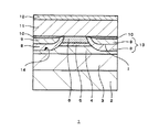
図1は、本発明に係る埋め込み型半導体レーザ素子の一実施の形態である。
本実施の形態の埋め込み型半導体レーザ素子1は、第1導電型のGaAs基板2上に順次、第1導電型のAlGaAsによる第1クラッド層3と、ノンドープのGaAsによる第1導電型の第1光ガイド層4と、窒素(N)を含むGaAs系による活性層、本例ではGaInNAsによる活性層を有する活性領域5と、ノンドープのGaAsによる第2導電型の第2光ガイド層6を積層し、メサエッチングによる除去部に電流を狭窄するための埋め込み層、いわゆる電流狭窄層(電流をブロックする電流ブロッキング層ともいう)13を形成し、さらに、第2光ガイド層6に接して第2導電型のAlGaAsによる第2クラッド層11、第2導電型のGaAsによるキャップ層12を積層して構成される。
そして、本実施の形態では、特に、メサエッチングをAlを含まない第2光ガイド層6からAlを含まない第1光ガイド層4の途中まで行い、第1、第2光ガイド層4、6及び活性層5を含めてAlを含まない再成長面14から成長して電流狭窄層13を形成するようにする。
Embodiments of the present invention will be described below with reference to the drawings.
FIG. 1 shows an embodiment of an embedded semiconductor laser device according to the present invention.
The buried type
In this embodiment, in particular, mesa etching is performed from the second
電流狭窄層13は、例えば、第1導電型の第1光ガイド層4に接する第2導電型の第1半導体層8とその上の第1導電型の第2半導体層9により、pn接合jを有するように形成することができる。電流狭窄層13の第1半導体層8と第2半導体層9としては、AlGaAsまたはGaAsで形成することができる。その他、電流狭窄層13は絶縁層により形成することも可能である。
さらに電流狭窄層13と第2クッラド層11との間に第1導電型のGaAsによるキャップ層10が形成される。
The
Further, a
活性領域5としては、例えばGaInNAsの活性層とGaAsのバリア層とによる量子井戸構造、例えば二重量子井戸(DQW)構造で形成することができる。活性領域5を構成する活性層としては、上述のGaInNAsの他、GaInNAsSb、GaAsSbN、またはGaNAs等で形成することができる。
メサエッチングによるメサ部は、共振器長方向にストライプ状に形成される。なお、図示せざるも第2導電型のキャップ層12の表面に一方の電極が形成され、第1導電型のGaAs基板2の裏面に他方の電極が形成される。
The
The mesa portion by mesa etching is formed in a stripe shape in the resonator length direction. Although not shown, one electrode is formed on the surface of the second conductivity
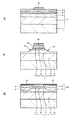
次に、図2〜図4を参照して本実施の形態の埋め込み型半導体レーザ素子1の製造方法一実施の形態を説明する。同図は好ましい実施の形態を示すが、前述しように各層の組成はこれに限定されず、また各層の組成比、膜厚等もこれに限定されない。
本実施の形態の埋め込み型半導体レーザ素子1は、主面(100)結晶面としたn型のGaAs基板2上に、n型Al0.2Ga0.8Asの第1クラッド層3を形成する、本例では、n型Al0.2Ga0.8Asの第1クラッド層3を膜厚2μm成長する(図2A参照)。次に、ノンドープGaAsの第1ガイド層4を形成する。本例では、第1ガイド層4を膜厚500nm成長する(図2B参照)。次に、GaInNAs層を有する活性領域5を成長する(図2C参照)。この活性領域5は、GaInNAsの活性層とGaAsのバリア層による二重量子井戸(DQW)構造に形成される。次に、ノンドープGaAsの第2ガイド層6を形成する。本例では、第2ガイド層6を膜厚500nm成長する。このようにして基板2上にn型第1クラッド層3、第1光ガイド層4、活性領域5及び第2光ガイド層6をMOCVD(有機金属化学気相成長)法で積層した基板7を形成する(図2D参照)。
Next, an embodiment of a manufacturing method of the embedded
In the buried
次に、基板7を取り出し、第2ガイド層6の上面にフォトリソグラフィー技術により、共振器長方向(紙面と直交する方向)に長いストライプパターンをなす耐エッチンマスク15を形成する。本例では、基板7の第2ガイド層6上に、例えば約3μmの幅のストライプパターンをなすSiO2マスク15を形成する(図3E参照)。単一横モード発振するためのメサ幅、すなわち、ストライプパターン幅は、横方向の光閉じ込めにより変えることができる。
Next, the
次に、ウエットエッチングによるメサエッチングによりメサ部16を形成する。このとき、メサエッチングは、GaAsの第1ガイド層4で停止させることが重要である(図3F参照)。n型Al0.2Ga0.8Asの第1クラッド層3までエッチングを行うと、Alを保有するn型Al0.2Ga0.8Asの第1クラッド層3が大気にさらされるため、酸素と結合してしまう。このAlと結合した酸素を取り除くことは困難である。GaAsの第1ガイド層3表面上では、AsH3中で700℃以上アニールを行えば、SIMS(Secondary Ion Mass Spectrometry)による検出限界以下まで酸素濃度を低減させることができる。また、エッチングを正確にとめるためには、さらにInGaPによるエッチングストップ層などを用いても良い。このメサエッチングにより、エッチング除去部の面、すなわちメサ部16の両側の再結晶成長面14は、第1、第2ガイド層4,6、活性領域5を含む全面がAlを含まない面となる。
Next, the
次に、メサ部16を形成した後、SiO2マスク15を除去せずに、MOCVD炉内に導入し、メサ部16の両側にn型AlGaAsの第1半導体層(いわゆる、第1電流狭窄層)8及びp型AlGaAsの第2半導体層(いわゆる、第2電流狭窄層)9を順次選択成長して電流狭窄層となる埋め込み層13を形成する。AlGaAsの第1電流狭窄層8,第2電流狭窄層9は、Al組成0.3以下が望ましい。それ以上では、電流狭窄層13の選択成長が困難となることに加え、レーザ素子の熱抵抗も上昇してしまう。本例では、第1、第2電流狭窄層8,9の組成比をAl0.1Ga0.9Asとする。次にn型GaAsの第1キャップ層10を形成する(図3G参照)。
Next, after the
次に選択成長後、基板7をMOCVD炉から取り出し、SiO2マスク15を除去する。SiO2マスク15の除去後、もう一度、基板7をMOCVD炉の中に導入し、p型AlGaAsの第2クラッド層11を形成する。本例では、組成比p型Al0.2Ga0.8Asの第2クラッド層11を膜厚約2μm成長する。
次に、第2クラッド層11上にp型GaAsの第2キャップ層12を成長する。次に、第2キャップ層12の上面にp型基板17を形成し、n型GaAs基板2の裏面にn型電極18を形成して、目的とする埋め込み型半導体レーザ素子1が完成する(図4参照)。
Next, after the selective growth, the
Next, a
通常の埋め込み型半導体レーザ素子では、GaAsのガイド層を厚くすると、活性層への光閉じ込めが弱くなってしまうため、それほどガイド層を厚くすることができない。しかし、GaInNAsの活性層は、通常のGaAs系材料に比べて屈折率が低くなるため、本実施の形態において、GaAsの第1、第2ガイド層4,6が厚くなっても、光を十分に活性層5内に閉じ込めることができる。そのため、光閉じ込めの低下によるしきい電流の増加も少ない。GaAsの第1、第2ガイド層4,6の厚さは、p型の第1電流狭窄層8及びn型の第2電流狭窄層9が、機能できる膜厚を必要とする。例えば、GaAsの第1、第2ガイド層4,6の厚さは、100nm以上が望ましい。第1、第2ガイド層4,6が、厚い場合には制限はないが、現実的な厚さとして、1μm以下が望ましいと考えられる。
In a typical buried semiconductor laser device, if the GaAs guide layer is thickened, the light confinement in the active layer becomes weak, so the guide layer cannot be made so thick. However, since the active layer of GaInNAs has a lower refractive index than that of a normal GaAs-based material, in this embodiment, even if the first and second guide layers 4 and 6 of GaAs become thick, sufficient light can be obtained. It can be confined in the
図5は、GaInNAsの活性層を用いた埋め込み型半導体レーザ従来のIn0.2Ga0.8Asの活性層を用いた埋め込み型半導体レーザとの光閉じ込めの比較を示すグラフである。
図5は光閉じ込め率のガイド層厚依存性を示す特性図であり、縦軸に光閉じ込め率(%)、横軸にガイド層厚さ(μm)を示す。但し、この図5のグラフは、通常のリッジ型半導体レーザのFFP(Far Field Pattern)から計算した屈折率から埋め込み型半導体レーザにしたときの光閉じ込めを見積もったデータで表した。
(実線)30は、波長1.3μm帯のGaInNAs活性層の半導体レーザの特性曲線(破線)31は、従来のIn0.2Ga0.8As活性層の半導体レーザの特性である。このグラフによれば、GaInNAs活性層レーザ(曲線30)は、従来のIn0.2Ga0.8As活性層レーザ(曲線31)の場合に比べて、バリア厚さのどの段階であっても光閉じ込め率がよくなっていることが分かる。
このGaInNAs活性層を備えた埋め込み型半導体レーザ素子は、信頼性が高く、かつ低しきい電流を実現することができる。
FIG. 5 is a graph showing a comparison of optical confinement with an embedded semiconductor laser using an active layer of conventional In 0.2 Ga 0.8 As, using an embedded semiconductor laser using an active layer of GaInNAs.
FIG. 5 is a characteristic diagram showing the dependence of the optical confinement ratio on the guide layer thickness, where the vertical axis indicates the optical confinement ratio (%) and the horizontal axis indicates the guide layer thickness (μm). However, the graph of FIG. 5 is represented by data obtained by estimating the optical confinement when the buried semiconductor laser is made from the refractive index calculated from the FFP (Far Field Pattern) of a normal ridge semiconductor laser.
(Solid line) 30 is a characteristic curve (dashed line) 31 of a semiconductor laser of a GaInNAs active layer having a wavelength of 1.3 μm band, and a
The buried type semiconductor laser device provided with the GaInNAs active layer is highly reliable and can realize a low threshold current.
上述の本実施の形態に係る埋め込み型半導体レーザ素子1によれば、GaAs系レーザであるため熱抵抗が低く、また例えばGaInNAs活性層などの窒素(N)を有する活性層はΔEcを大きく取れるために、従来のInP系半導体レーザ素子に比べて、温度特性に優れるものである。温度特性に優れることから、本実施の形態の埋め込み型半導体レーザ素子1は、冷却装置のないアンクール半導体レーザ素子にてきしている。また、GaAs基板2は安価で大口径化可能である。したがって、優れた特性を有する埋め込み型半導体レーザ素子を安価に実現することができる。
According to the embedded
さらに、本実施の形態に係る埋め込み型半導体レーザ素子1において、活性層となるGaInNAs層は屈折率が小さくなるため、GaAsガイド層4、6を厚く形成するおとが可能になる。これによって、Alを含む層、すなわちAlGaAsの第1クラッド層3を大気にさらすことなく、埋め込み層による電流狭窄層13を形成することができ、信頼性の高い埋め込み型半導体レーザ素子1を実現できる。つまり、再成長界面に、素子劣化の原因となる酸素を残さずに埋め込み型半導体レーザ素子を作製することができる。
Further, in the buried
本実施の形態に係る半導体レーザ素子1の製法によれば、GaInNAsを活性領域5に用いることで、第1ガイド層4及び第2ガイド層6を厚く形成することができ、信頼性の高い埋め込み型半導体レーザ素子1を作製することができる。
According to the manufacturing method of the
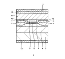
図6は、本発明に係る埋め込み型半導体レーザ素子を用いた第2実施例を示す。
通常、光通信では、単一波長で発振するDFB(Distributed Feedback)レーザが用いられる。本実施の形態は、DFB(分布帰還型)化した埋め込み型半導体レーザ素子に適用した場合である。
本実施の形態に係る埋め込み型半導体レーザ素子21は、第1導電型のGaAs基板2上に順次、第1導電型のAlGaAsによる第1クラッド層3と、ノンドープのGaAsによる第1導電型の第1光ガイド層4aを途中まで成長する。その後、エッチングにより回折格子を作成し、次いでAlGaAs層を回折格子が平坦に埋まるように成長速度を下げて成長して回折格子層22を形成する。その後、回折格子層22上にGaAs光ガイド層4bを追加し、続けて窒素(N)を含むGaAs系による活性層、本例ではGaInNAsによる活性層を有する活性領域5と、ノンドープのGaAsによる第2導電型の第2光ガイド層6を積層する。その後、メサエッチングによる除去部に電流を狭窄するための埋め込み層、いわゆる電流狭窄層(電流をブロックする電流ブロッキング層ともいう)13を形成する。このとき、Alを含む回折格子22部分までエッチングしないようにする。これにより、Alを含む面が大気にさらされることはない。さらに、第2導電型のAlGaAsによる第2クラッド層11、第2導電型のGaAsによるキャップ層12を積層してレーザ構造が構成される。
FIG. 6 shows a second embodiment using the embedded semiconductor laser device according to the present invention.
Usually, in optical communication, a DFB (Distributed Feedback) laser that oscillates at a single wavelength is used. The present embodiment is a case where the present invention is applied to a buried semiconductor laser device that is made into a DFB (distributed feedback type).
The buried
回折格子層22は、図6Bに示すように、例えばGaAs層23とAlGaAs層(例えばAl0.1Ga0.9As層)24とが、共振器長方向に繰り返し配列されて形成される。各層23、24の配列方向の幅dは10nm〜50nmに程度にすることができる。回折格子層22を構成する一方の層24は、AlGaAsに限ることなく、他方のGaAs層23と屈折率差があり、回折格子を形成できる材料層であればよい。例えば層23としてはGaAs(Sb)(N)層(すなわち、GaAsSbN層、GaAsSb層もしくはGaAsN層)とGaAs層、または、GaInNAs(Sb)層(すなわち、GaInNAsSb層もしくはGaInNAs層)とGaAs層などでもよい。
また、図6Cのように、回折格子部分は、表面積が非常に小さいため、Al組成が0.2以下であれば、活性層のメサ上部に回折格子を作製しても、信頼性が大きく低下することはない。さらに、回折格子部分がAlを含まない材料で構成される場合には、活性層の上に回折格子を作製しても、信頼性に問題はない。
As shown in FIG. 6B, the
In addition, as shown in FIG. 6C, since the surface area of the diffraction grating portion is very small, if the Al composition is 0.2 or less, the reliability is greatly reduced even if the diffraction grating is formed on the mesa of the active layer. Never do. Furthermore, when the diffraction grating portion is made of a material not containing Al, there is no problem in reliability even if the diffraction grating is formed on the active layer.
本実施の形態では、メサエッチングをAlを含まない第2光ガイド層6からAlを含まない第1光ガイド層4bの途中まで行い、第1、第2光ガイド層4a、4b、6、活性層5及び回折格子層22を含めたAlを含まない再成長面14から成長して電流狭窄層13が形成される。ここで、回折格子層22ではAlGaAs層24を有する場合でも、面積的に極めて小さく、また活性層から離れているため、信頼性に大きな影響は与えない。
In the present embodiment, mesa etching is performed from the second
電流狭窄層13としては、前述と同様に好ましくは第2導電型の第1半導体層8とその上の第1導電型の第2半導体層9により。pn接合jを有する半導体層で形成する。その他、絶縁層で形成することも可能である。電流狭窄層13と第2クラッド層11との間に第1導電型のGaAsによるキャップ層10が形成される。
活性領域5は、前述と同様に例えばGaInNAsの活性層とGaAsのバリア層とによる量子井戸構造、例えば二重量子井戸(DQW)構造で形成することができる。活性領域5を構成する活性層は、上述のGaInNAsの他、GaInNAsSb、GaAsSbN、またはGaNAs等で形成することができる。
The
The
次に、DFB化した本実施の形態の埋め込み型半導体レーザ素子21の製造方法を説明する。
先ず、上述した埋め込み型半導体レーザ素子1と同様に、主面を(100)結晶面としたn型GaAs基板2上に、n型AlGaAsの第1クラッド層3、ノンドープGaAsの第1ガイド層4aを途中まで成長する。その後、表面にフォトレジスト層を形成し電子ビーム(EB)露光装置により回折格子パターンに露光し、現像処理する。すなわち、共振器長方向に所要間隔を置いて開口を有するレジストマスクを形成する。次にレジストマスクを介してノンドープGaAsの第1のガイド層4aの表面部分をドライエッチングして所要間隔を置いて繰り返す凹部を形成する。本例では、回折格子パターンは、10〜50nm程度でドライエッチングを行う。
Next, a manufacturing method of the embedded
First, in the same manner as the above-described buried type
次に、レジストを剥離し、前処理を施した後、凹凸状の第1ガイド層4aの表面に凹部を埋めるように成長速度を遅くしてAlGaAs層を成長する。この成長層は、AlGaAs層に限ることはない。GaAs層と屈折率差があり、回折格子22を形成できればよい。例えば、GaInNAs層やGaNAsSbなどでもよい。これらの材料を回折格子に使うと、吸収回折格子型DFBを作製することも可能である。回折格子22の深さ及び埋め込み層の組成を変えるとDFBの特性が変化する。用途に合わせてパラメータを決めることが望ましい。その後、残りのGaAs光ガイド層4b、GaInNAs層を有する活性領域5、ノンドープGaAsの第2ガイド層6を形成することで2回目のエピタキシャル成長が終了する。
これ以降は、前述の図3E〜図4と同様の工程を経ることにより、図6に示す目的のDFB化した埋め込み型半導体レーザ素子21を得ることができる。このとき、回折格子層までエッチングしないようにすれば、再成長表面にAlを含む層がでることはない。
Next, after removing the resist and pre-treating, an AlGaAs layer is grown at a slow growth rate so as to fill the recesses in the surface of the uneven
Thereafter, the target DFB-embedded embedded
本実施の形態に係る埋め込み型半導体レーザ素子21によれば、温度特性に優れ信頼性の高いDFB化された半導体レーザ素子を提供することができる。また、GaInNAs当の窒素(N)を有する活性層に用いることで、ガイド層を厚く形成することができるため、信頼性の高いBH−DFB半導体レーザ素子を作製できる。
According to the embedded
以上は、本発明による半導体レーザ素子の実施の形態について説明したが、この実施の形態に限られるものではなく、本発明の要素を逸脱しない範囲でその他、様々な構成を取り得る。 Although the embodiment of the semiconductor laser device according to the present invention has been described above, the present invention is not limited to this embodiment, and various other configurations can be taken without departing from the elements of the present invention.
1・・埋め込み型半導体レーザ素子、2・・第1導電型のGaAs基板、3・・第1クラッド層、4、4a、4b・・第1導電型の第1光ガイド層、5・・活性領域、6・・第2導電型の第2光ガイド層、7・・基板、8・・第1電流狭窄層、9・・第2電流狭窄層、10・・第1キャップ層、11・・第2クラッド層、12・・キャップ層、13・・電流狭窄層、14・・再成長面、15・・SiO2マスク、16・・メサ部、17・・p型基板、21・・埋め込み型半導体レーザ素子、22・・回折格子層、23・・GaAs層、24・・AlGaAs層、
1 .. Embedded
Claims (2)
第1導電型のAlGaAsの第1クラッド層と、
ノンドープGaAsの第1ガイド層と、
GaInNAs、GaInNAsSb、GaAsSbNまたはGaNAsの活性層と、
ノンドープGaAsの第2ガイド層と、
第2導電型AlGaAsの第2クラッド層が順次積層された積層体と、
前記第2ガイド層の表面から前記第1ガイド層の途中までメサエッチングされて形成されたメサ部のAlを含まない再結晶成長面から順次成長された第2導電型AlGaAsまたはGsAsの第1電流狭窄層及び第1導電型AlGaAsまたはGaAsの第2電流狭窄層からなる電流をブロックする埋め込み層と、
前記第2電流狭窄層と前記第2クラッド層との間に形成された第1導電型GaAsのキャップ層と
を有する
埋め込み型半導体レーザ素子。 On the first conductivity type GaAs substrate,
A first cladding layer of AlGaAs of the first conductivity type;
A first guide layer of non-doped GaAs;
An active layer of GaInNAs, GaInNAsSb, GaAsSbN or GaNAs;
A second guide layer of non-doped GaAs;
A stacked body in which second cladding layers of second conductivity type AlGaAs are sequentially stacked;
The first current of the second conductivity type AlGaAs or GsAs sequentially grown from the recrystallized growth surface not containing Al in the mesa portion formed by mesa etching from the surface of the second guide layer to the middle of the first guide layer. A buried layer for blocking current comprising a constriction layer and a second current confinement layer of a first conductivity type AlGaAs or GaAs;
A cap layer of a first conductivity type GaAs formed between the second current confinement layer and the second cladding layer;
Buried type semiconductor laser device having a.
請求項1記載の埋め込み型半導体レーザ素子。 2. The buried semiconductor laser device according to claim 1, further comprising a diffraction grating layer formed of an AlGaAs layer and a GaAs layer, a GaInNAsSb layer or a GaInNAs layer and a GaAs layer, or a GaAsSbN layer, a GaAsSb layer or a GaAsN layer and a GaAs layer .
Priority Applications (1)
| Application Number | Priority Date | Filing Date | Title |
|---|---|---|---|
| JP2004048289A JP4617684B2 (en) | 2004-02-24 | 2004-02-24 | Semiconductor laser element |
Applications Claiming Priority (1)
| Application Number | Priority Date | Filing Date | Title |
|---|---|---|---|
| JP2004048289A JP4617684B2 (en) | 2004-02-24 | 2004-02-24 | Semiconductor laser element |
Publications (3)
| Publication Number | Publication Date |
|---|---|
| JP2005243722A JP2005243722A (en) | 2005-09-08 |
| JP2005243722A5 JP2005243722A5 (en) | 2006-10-12 |
| JP4617684B2 true JP4617684B2 (en) | 2011-01-26 |
Family
ID=35025163
Family Applications (1)
| Application Number | Title | Priority Date | Filing Date |
|---|---|---|---|
| JP2004048289A Expired - Fee Related JP4617684B2 (en) | 2004-02-24 | 2004-02-24 | Semiconductor laser element |
Country Status (1)
| Country | Link |
|---|---|
| JP (1) | JP4617684B2 (en) |
Families Citing this family (3)
| Publication number | Priority date | Publication date | Assignee | Title |
|---|---|---|---|---|
| CN100382347C (en) * | 2005-10-20 | 2008-04-16 | 中国科学院半导体研究所 | Gallium arsenide-based 1.5 micron quantum well structure and its epitaxial growth method |
| JP2007258269A (en) | 2006-03-20 | 2007-10-04 | Sumitomo Electric Ind Ltd | Semiconductor optical element |
| JP2008211142A (en) * | 2007-02-28 | 2008-09-11 | Nippon Telegr & Teleph Corp <Ntt> | Optical semiconductor device |
Citations (4)
| Publication number | Priority date | Publication date | Assignee | Title |
|---|---|---|---|---|
| JPH1174607A (en) * | 1997-06-23 | 1999-03-16 | Sharp Corp | Semiconductor laser |
| JP2000012971A (en) * | 1998-06-19 | 2000-01-14 | Nec Corp | Semiconductor laser |
| JP2000505600A (en) * | 1996-02-27 | 2000-05-09 | テレフオンアクチーボラゲツト エル エム エリクソン(パブル) | Embedded heterostructure |
| JP2001223437A (en) * | 2000-02-07 | 2001-08-17 | Hitachi Ltd | Semiconductor laser device |
-
2004
- 2004-02-24 JP JP2004048289A patent/JP4617684B2/en not_active Expired - Fee Related
Patent Citations (4)
| Publication number | Priority date | Publication date | Assignee | Title |
|---|---|---|---|---|
| JP2000505600A (en) * | 1996-02-27 | 2000-05-09 | テレフオンアクチーボラゲツト エル エム エリクソン(パブル) | Embedded heterostructure |
| JPH1174607A (en) * | 1997-06-23 | 1999-03-16 | Sharp Corp | Semiconductor laser |
| JP2000012971A (en) * | 1998-06-19 | 2000-01-14 | Nec Corp | Semiconductor laser |
| JP2001223437A (en) * | 2000-02-07 | 2001-08-17 | Hitachi Ltd | Semiconductor laser device |
Also Published As
| Publication number | Publication date |
|---|---|
| JP2005243722A (en) | 2005-09-08 |
Similar Documents
| Publication | Publication Date | Title |
|---|---|---|
| JP4639107B2 (en) | Semiconductor laser and manufacturing method thereof | |
| US8273585B2 (en) | Optical semiconductor device and method for manufacturing the same | |
| US7638792B2 (en) | Tunnel junction light emitting device | |
| JP5026905B2 (en) | Semiconductor light emitting device and manufacturing method thereof | |
| US20120236890A1 (en) | P-type isolation regions adjacent to semiconductor laser facets | |
| US8514902B2 (en) | P-type isolation between QCL regions | |
| US8802468B2 (en) | Semiconductor light emitting device and fabrication method for semiconductor light emitting device | |
| JP5051054B2 (en) | Semiconductor laser and method of manufacturing the semiconductor laser | |
| JPH07154024A (en) | Semiconductor laser | |
| US7817691B2 (en) | Light emitting device | |
| JP3859839B2 (en) | Refractive index semiconductor laser device | |
| JP4617684B2 (en) | Semiconductor laser element | |
| JP4599700B2 (en) | Distributed feedback laser diode | |
| JP2001057459A (en) | Semiconductor laser | |
| JP2006216752A (en) | Manufacturing method for diffraction grating and semiconductor laser | |
| JP4718309B2 (en) | Optical semiconductor device | |
| JP2005093634A (en) | Surface emitting semiconductor laser and manufacturing method thereof | |
| JP4117557B2 (en) | Semiconductor laser device and manufacturing method thereof | |
| JP2003304029A (en) | Wavelength variable semiconductor laser device and wave length variable semiconductor laser integrated device | |
| JP3715639B2 (en) | Semiconductor light emitting device | |
| JP2003060312A (en) | Semiconductor laser element | |
| JP2007273817A (en) | Surface light emitting type semiconductor laser element and its manufacturing method | |
| JPH053364A (en) | Semiconductor laser | |
| JP2006019617A (en) | Semiconductor laser | |
| JP2001230488A (en) | Semiconductor laser device |
Legal Events
| Date | Code | Title | Description |
|---|---|---|---|
| A521 | Written amendment |
Free format text: JAPANESE INTERMEDIATE CODE: A523 Effective date: 20060824 |
|
| A621 | Written request for application examination |
Free format text: JAPANESE INTERMEDIATE CODE: A621 Effective date: 20060824 |
|
| A977 | Report on retrieval |
Free format text: JAPANESE INTERMEDIATE CODE: A971007 Effective date: 20091127 |
|
| A131 | Notification of reasons for refusal |
Free format text: JAPANESE INTERMEDIATE CODE: A131 Effective date: 20091208 |
|
| A521 | Written amendment |
Free format text: JAPANESE INTERMEDIATE CODE: A523 Effective date: 20100201 |
|
| TRDD | Decision of grant or rejection written | ||
| A01 | Written decision to grant a patent or to grant a registration (utility model) |
Free format text: JAPANESE INTERMEDIATE CODE: A01 Effective date: 20100928 |
|
| A01 | Written decision to grant a patent or to grant a registration (utility model) |
Free format text: JAPANESE INTERMEDIATE CODE: A01 |
|
| A61 | First payment of annual fees (during grant procedure) |
Free format text: JAPANESE INTERMEDIATE CODE: A61 Effective date: 20101011 |
|
| FPAY | Renewal fee payment (event date is renewal date of database) |
Free format text: PAYMENT UNTIL: 20131105 Year of fee payment: 3 |
|
| FPAY | Renewal fee payment (event date is renewal date of database) |
Free format text: PAYMENT UNTIL: 20131105 Year of fee payment: 3 |
|
| LAPS | Cancellation because of no payment of annual fees |