JP4613727B2 - Electrophoretic display device driving method, driving circuit, electrophoretic display device, and electronic apparatus - Google Patents
Electrophoretic display device driving method, driving circuit, electrophoretic display device, and electronic apparatus Download PDFInfo
- Publication number
- JP4613727B2 JP4613727B2 JP2005209302A JP2005209302A JP4613727B2 JP 4613727 B2 JP4613727 B2 JP 4613727B2 JP 2005209302 A JP2005209302 A JP 2005209302A JP 2005209302 A JP2005209302 A JP 2005209302A JP 4613727 B2 JP4613727 B2 JP 4613727B2
- Authority
- JP
- Japan
- Prior art keywords
- electrode
- voltage
- display device
- period
- electrophoretic display
- Prior art date
- Legal status (The legal status is an assumption and is not a legal conclusion. Google has not performed a legal analysis and makes no representation as to the accuracy of the status listed.)
- Expired - Lifetime
Links
Images


Landscapes
- Electrochromic Elements, Electrophoresis, Or Variable Reflection Or Absorption Elements (AREA)
- Control Of Indicators Other Than Cathode Ray Tubes (AREA)
Description
本発明は、電気泳動粒子を含有する分散系を有する電気泳動表示装置並びにその駆動方法、駆動回路および電子機器に関する。 The present invention relates to an electrophoretic display device having a dispersion system containing electrophoretic particles, a driving method thereof, a driving circuit, and an electronic apparatus.
非発光型の表示デバイスとして、電気泳動現象を利用した電気泳動表示装置が知られている。電気泳動現象は、液体中(分散媒)に微粒子(電気泳動粒子)を分散させた分散系に電界を印加したときに、微粒子が移動する現象である。基本的に、電気泳動表示装置は、一定間隔を隔てて対向した1対の電極と、これらの電極間に封入された分散系とを有している。そして、両電極間に電位差を与えると、帯電した電気泳動粒子が、電界の方向応じてどちらか一方の電極に引き付けられることになる。ここで、分散媒を染料で染色するとともに電気泳動粒子を顔料粒子で構成すれば、観測者には、電気泳動粒子の色または染料の色が見えることになる。 As a non-luminous display device, an electrophoretic display device using an electrophoretic phenomenon is known. The electrophoresis phenomenon is a phenomenon in which fine particles move when an electric field is applied to a dispersion system in which fine particles (electrophoretic particles) are dispersed in a liquid (dispersion medium). Basically, an electrophoretic display device has a pair of electrodes opposed to each other at a predetermined interval, and a dispersion system sealed between these electrodes. When a potential difference is applied between the two electrodes, the charged electrophoretic particles are attracted to one of the electrodes depending on the direction of the electric field. Here, if the dispersion medium is dyed with a dye and the electrophoretic particles are composed of pigment particles, the observer can see the color of the electrophoretic particles or the color of the dye.
しかしながら、アクティブマトリックス形式の電気泳動表示装置については、従来例がなく、その駆動方法や駆動回路については知られていない。 However, there is no conventional example of an active matrix type electrophoretic display device, and its driving method and driving circuit are not known.
本発明は上述した事情に鑑みてなされたものであり、その目的は、所望の階調表示を実現する電気泳動表示装置、特に、アクティブマトリックス形式の電気泳動表示装置の駆動方法、駆動回路および電子機器を提供することにある。 The present invention has been made in view of the above-described circumstances, and an object thereof is an electrophoretic display device that realizes a desired gradation display, in particular, a driving method, a drive circuit, and an electronic device for an active matrix type electrophoretic display device. To provide equipment.
本発明は、一の態様において、第1の電極及び第2の電極と、前記第1の電極と前記第2の電極との間に配置された、電気泳動粒子を含有する分散系と、複数の走査線と、前記複数の走査線と交差する複数のデータ線と、前記データ線と前記走査線との交差に対応して設けられ、前記データ線、前記走査線、及び前記第1の電極に電気的に接続されたスイッチング素子と、を備えた電気泳動表示装置の駆動方法であって、表示階調に対応した位置へ前記電気泳動粒子を移動させるために、前記表示階調に対応した値の電圧を、前記第1の電極および前記第2の電極の間に印加するステップを有することを特徴とする電気泳動表示装置の駆動方法を提供する。In one aspect, the present invention provides a first electrode and a second electrode, a dispersion system containing electrophoretic particles disposed between the first electrode and the second electrode, and a plurality of dispersion systems. Scan lines, a plurality of data lines intersecting with the plurality of scan lines, and the data lines, the scan lines, and the first electrodes. And a switching element electrically connected to the display device, wherein the electrophoretic particles are moved to a position corresponding to the display gradation and correspond to the display gradation. There is provided a driving method of an electrophoretic display device comprising a step of applying a voltage of a value between the first electrode and the second electrode.
好ましい態様において、前記表示階調に対応した値の電圧を印加するステップは、1水平走査期間にわたって前記走査線に選択電圧を供給することにより前記スイッチング素子をオン状態とし、前記データ線と前記第1の電極とを接続するステップと、前記スイッチング素子がオン状態となった前記水平走査期間のうち少なくとも一部の期間において、前記第1の電極と前記第2の電極との間に前記表示階調に対応した値の電圧を生じさせるための信号を、前記データ線及び前記スイッチング素子を介して前記第1の電極に供給するステップと、を有する。In a preferred aspect, in the step of applying a voltage having a value corresponding to the display gradation, the switching element is turned on by supplying a selection voltage to the scanning line over one horizontal scanning period, and the data line and the first line are turned on. And connecting the first electrode to the display floor between the first electrode and the second electrode in at least a part of the horizontal scanning period in which the switching element is turned on. Supplying a signal for generating a voltage having a value corresponding to a tone to the first electrode via the data line and the switching element.
他の好ましい態様において、前記スイッチング素子がオン状態となった前記水平走査期間において、前記一部の期間の後に、前記第1の電極と前記第2の電極との間の電圧が前記電気泳動粒子の泳動を停止させる電圧となるような信号を、前記データ線及び前記スイッチング素子を介して前記第1の電極に供給する。In another preferable aspect, in the horizontal scanning period in which the switching element is in an ON state, the voltage between the first electrode and the second electrode is changed to the electrophoretic particle after the partial period. A signal that provides a voltage for stopping the migration of the first electrode is supplied to the first electrode through the data line and the switching element.
さらに他の好ましい態様において、前記表示階調に対応した値の電圧を印加するステップは、第1の水平走査期間において前記走査線に選択電圧を供給することにより前記スイッチング素子をオン状態とし、前記データ線と前記第1の電極とを接続するステップと、前記第1の水平走査期間において、前記第1の電極と前記第2の電極との間に前記表示階調に対応した値の電圧を生じさせるための信号を、前記データ線及び前記スイッチング素子を介して前記第1の電極に供給するステップと、前記第1の水平走査期間より後の第2の水平走査期間において前記走査線に選択電圧を供給することにより前記スイッチング素子をオン状態とし、前記データ線と前記第1の電極とを接続するステップと、前記第2の水平走査期間において、前記第1の電極と前記第2の電極との間の電圧が前記電気泳動粒子の泳動を停止させる電圧となるような信号を、前記データ線及び前記スイッチング素子を介して前記第1の電極に供給する。In still another preferred aspect, the step of applying a voltage having a value corresponding to the display gradation turns on the switching element by supplying a selection voltage to the scanning line in a first horizontal scanning period, and In the step of connecting the data line and the first electrode, and in the first horizontal scanning period, a voltage having a value corresponding to the display gradation is applied between the first electrode and the second electrode. A signal to be generated is supplied to the first electrode via the data line and the switching element, and the scanning line is selected in a second horizontal scanning period after the first horizontal scanning period. Supplying the voltage to turn on the switching element to connect the data line and the first electrode; and in the second horizontal scanning period, Supplying a signal, such as voltage becomes a voltage for stopping the migration of the electrophoretic particles, the first electrode through the data line and the switching element between the electrode and the second electrode.
更に他の好ましい態様において、前記第1の水平走査期間は、第1のフィールド期間に含まれ、前記第2の水平走査期間は、前記第1のフィールド期間より後の第2のフィールド期間に含まれる。In still another preferred aspect, the first horizontal scanning period is included in a first field period, and the second horizontal scanning period is included in a second field period after the first field period. It is.
更に他の好ましい態様において、前記表示階調に対応した値の電圧を印加するステップの前に、前記第1の電極および前記第2の電極の間にリセット電圧を印加することにより、前記電気泳動粒子を、前記分散系中において前記第1電極側または前記第2電極側へ引き寄せるリセットステップをさらに有する。In still another preferred aspect, the electrophoresis is performed by applying a reset voltage between the first electrode and the second electrode before applying the voltage corresponding to the display gradation. The method further includes a reset step of attracting the particles toward the first electrode or the second electrode in the dispersion.
本発明は、他の観点において、第1の電極及び第2の電極と、前記第1の電極と前記第2の電極との間に配置された、電気泳動粒子を含有する分散系と、複数の走査線と、前記複数の走査線と交差する複数のデータ線と、前記データ線と前記走査線との交差に対応して設けられ、前記データ線、前記走査線、及び前記第1の電極に電気的に接続されたスイッチング素子と、を有する電気泳動表示装置の駆動回路であって、表示階調に対応した位置へ前記電気泳動粒子を移動させるために、前記表示階調に対応した値の電圧を、前記第1の電極および前記第2の電極の間に印加することを特徴とする電気泳動表示装置の駆動回路を提供する。In another aspect, the present invention provides a first electrode and a second electrode, a dispersion system containing electrophoretic particles disposed between the first electrode and the second electrode, and a plurality of dispersion systems. Scan lines, a plurality of data lines intersecting with the plurality of scan lines, and the data lines, the scan lines, and the first electrodes. And a switching element electrically connected to the driving circuit of the electrophoretic display device, the value corresponding to the display gradation in order to move the electrophoretic particles to a position corresponding to the display gradation Is applied between the first electrode and the second electrode. A driving circuit for an electrophoretic display device is provided.
本発明は、さらに他の観点において、第1の電極及び第2の電極と、前記第1の電極と前記第2の電極との間に配置された、電気泳動粒子を含有する分散系と、複数の走査線と、前記複数の走査線と交差する複数のデータ線と、前記データ線と前記走査線との交差に対応して設けられ、前記データ線、前記走査線、及び前記第1の電極に電気的に接続されたスイッチング素子とを備え、表示階調に対応した位置へ前記電気泳動粒子を移動させるために、前記表示階調に対応した値の電圧が、前記第1の電極および前記第2の電極の間に印加されることを特徴とする電気泳動表示装置を提供する。In still another aspect, the present invention provides a first electrode and a second electrode, and a dispersion system containing electrophoretic particles disposed between the first electrode and the second electrode, A plurality of scanning lines, a plurality of data lines intersecting with the plurality of scanning lines, and the intersections of the data lines and the scanning lines, the data lines, the scanning lines, and the first A switching element electrically connected to the electrode, and in order to move the electrophoretic particles to a position corresponding to the display gradation, a voltage corresponding to the display gradation is applied to the first electrode and An electrophoretic display device is provided between the second electrodes.
本発明は、さらに他の観点において、上記電気泳動表示装置を備えることを特徴とする電子機器を提供する。In still another aspect, the present invention provides an electronic apparatus comprising the electrophoretic display device.
なお、本発明に係る電子機器は、電気泳動装置を表示部として用いることを特徴とするものであって、例えば、電子書籍、パーソナルコンピュータ、携帯電話、電子広告掲示板、電子道路標識等がこれに該当する。 The electronic apparatus according to the present invention is characterized by using an electrophoretic device as a display unit, such as an electronic book, a personal computer, a mobile phone, an electronic bulletin board, and an electronic road sign. Applicable.
以上説明したように、本発明によれば、電気泳動現象を用いて所望の階調表示を実現させることができる。 As described above, according to the present invention, a desired gradation display can be realized using the electrophoresis phenomenon.
以下、本発明の実施の形態について、図面を参照して説明する。
A:第1実施形態
第1実施形態に係る電気泳動表示装置は、入力画像信号VIDに応じた画像を表示するものであり、静止画・動画のいずれにおいても表示が可能であるが、特に、静止画の表示に適している。
Embodiments of the present invention will be described below with reference to the drawings.
A: First Embodiment The electrophoretic display device according to the first embodiment displays an image according to the input image signal VID, and can display both a still image and a moving image. Suitable for displaying still images.
A−1:電気泳動表示装置の全体構成
本実施形態の電気泳動表示装置は、電気泳動表示パネルと周辺回路とを備えている。まず、電気泳動表示パネルの機械的な構成について説明する。図1は本発明の一実施形態に係る電気泳動表示パネルAの機械的な構成を示す分解斜視図であり、図2は、その部分断面図である。
A-1: Overall Configuration of Electrophoretic Display Device The electrophoretic display device of this embodiment includes an electrophoretic display panel and a peripheral circuit. First, the mechanical configuration of the electrophoretic display panel will be described. FIG. 1 is an exploded perspective view showing a mechanical configuration of an electrophoretic display panel A according to an embodiment of the present invention, and FIG. 2 is a partial sectional view thereof.
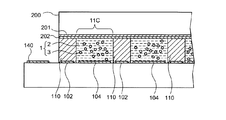
図1および図2に示すように電気泳動表示パネルAは、画素電極104等が形成されたガラスや半導体等の素子基板100と、平面状の共通電極201等が形成された対向基板200とを有している。素子基板100と、対向基板200は、一定の間隙を保って、各々の電極形成面が対向するように貼り合わされている。素子基板100と対向基板200とに挟まれた空間は、一定の高さを持った隔壁110によって仕切られている。この例では、隔壁110は、画像の表示単位である画素を区分けするように設けられている。隔壁110によって仕切られた空間は分割セル11Cと呼ばれ、そこには分散系1が充填されている。
As shown in FIGS. 1 and 2, an electrophoretic display panel A includes an
この分散系1は、分散媒2に電気泳動粒子3を分散させたものである。分散媒2は、界面活性剤等の添加剤が必要に応じて添加されている。分散系1では、電気泳動粒子3の重力による沈降を避けるため、分散媒2の比重と電気泳動粒子3の比重は略等しくなるように選ばれている。
This
このように隔壁110によって、多数の分割セル11Cを設けたので、電気泳動粒子3が泳動可能な領域が分割セル11Cの内部に制限されることになる。分散系1には、粒子の分散が偏ったり、あるいは、複数の粒子が結合して大きな塊になる凝結が起きることがある。上述したように隔壁110を用いて複数の分割セル11Cを形成すると、そのような現象を防ぐことができ、表示画像の品質を向上させることが可能となる。
As described above, the
電気泳動表示パネルAは、フルカラー表示が可能である。この場合には、各画素において原色(RGB)のうち1色を表示できるようにするため、分散系1としては、赤色、緑色、青色に対応する3種類が用いられる。
The electrophoretic display panel A is capable of full color display. In this case, three types corresponding to red, green, and blue are used as the
まず、赤色に対応する分散系1rは、電気泳動粒子3rとして赤色の粒子を用いるとともに、分散媒2rとしてシアン色のものを用いることができる。この電気泳動粒子3rとしては、例えば、酸化鉄を用いることができる。次に、緑色に対応する分散系1gは、電気泳動粒子3gとして緑色の粒子を用いるとともに、分散媒2gとしてマゼンダ色のものを用いることができる。この電気泳動粒子3gとしては、例えば、コバルトグリーンの顔料粒子を用いることができる。次に、青色に対応する分散系1bは、電気泳動粒子3bとして青色の粒子を用いるとともに、分散媒2bとしてイエロー色のものを用いることができる。この電気泳動粒子2bとしては、例えば、コバルトブルーの顔料粒子を用いることができる。 First, in the dispersion system 1r corresponding to red, red particles can be used as the electrophoretic particles 3r, and cyan particles can be used as the dispersion medium 2r. For example, iron oxide can be used as the electrophoretic particles 3r. Next, in the dispersion system 1g corresponding to green, green particles can be used as the electrophoretic particles 3g and magenta can be used as the dispersion medium 2g. For example, cobalt green pigment particles can be used as the electrophoretic particles 3g. Next, in the dispersion system 1b corresponding to blue, blue particles can be used as the electrophoretic particles 3b, and yellow particles can be used as the dispersion medium 2b. As the electrophoretic particles 2b, for example, cobalt blue pigment particles can be used.
すなわち、電気泳動粒子3として表示色を反射するものを用いる一方、分散媒2として表示色を吸収する色(上述した例では補色)に対応したものを用いる。また、対向基板200、共通電極201および封止材202の部材を用いる。よって、電気泳動粒子3が表示面側の電極に浮上しているのであれば、電気泳動粒子3によって表示色に対応する波長の光が反射され、この反射光によって観測者は色を認識する。一方、電気泳動粒子3が表示面と反対側の電極に沈降しているのであれば、表示色に対応する波長の光は分散媒2によって吸収されるため、その波長の光が観測者に届かないので観測者は色を認識できない。ところで、分散系1に印加する電界の方向と強度によって、電気泳動粒子3を分散系1の厚さ方向にどのように分布させるかを制御できる。したがって、電気泳動粒子3とその反射光を吸収する分散媒2と組み合わせて用いるとともに電界強度を制御することによって、電気泳動粒子3によって反射される光の反射強度を調整でき、この結果、観測者に到達する光の強度を変化させることができる。
That is, the
次に、素子基板100の表面には、表示領域A1と、周辺領域A2とが設けられている。表示領域A1は、隔壁110によって、仕切られており、そこには、画素電極104の他に、後述する走査線、データ線、およびスイチッング素子として機能する薄膜トランジスタ(Thin Film Transistor:以下、TFTと称する)が形成されるようになっている。一方、素子基板100の周辺領域A2には、後述する走査線駆動回路、データ線駆動回路、および外部接続電極が形成されるようになっている。
Next, a display area A1 and a peripheral area A2 are provided on the surface of the
図3は電気泳動表示装置の電気的な構成を示すブロック図である。この図に示すように電気泳動表示装置は、電気泳動表示パネルAとその周辺回路である画像信号処理回路300Aおよびタイミングジェネレータ400を備えている。ここで、画像信号処理回路300Aは、入力画像信号VIDに、電気泳動表示パネルAの電気的な特性に応じた補正処理を施して画像データDを生成出力するとともに、この画像データDを出力する前に、リセットデータDrestを所定期間出力する。リセットデータDrestは分散系1中を泳動している電気泳動粒子3を画素電極104側に引き寄せ、その空間的な状態を初期化するために用いられる。以下では、説明を簡略化するため分散系1の分散媒2は黒色に着色されており、電気泳動粒子3は酸化チタン等の白色の粒子で且つ、正に帯電しているものとする。
FIG. 3 is a block diagram showing an electrical configuration of the electrophoretic display device. As shown in this figure, the electrophoretic display device includes an electrophoretic display panel A, an image
また、タイミングジェネレータ400は、画像データDが画像信号処理回路300Aから出力されるときのみ、走査線駆動回路130やデータ線駆動回路140Aを制御するための各種タイミング信号を生成する。
The
素子基板100の表示領域A1には、X方向に沿って平行に複数本の走査線101が形成され、また、これと直交するY方向に沿って平行に複数本のデータ線102が形成されている。そして、これらの走査線101とデータ線102との各交点においては、TFT103のゲート電極が走査線101に接続される一方、そのソース電極がデータ線102に接続され、さらに、そのドレイン電極が画素電極104に接続されている。各画素は、画素電極104と、対向基板200に形成された共通電極201と、これら両電極間に挟持された分散系1とによって構成される(図2参照)。すなわち、各画素は、走査線101とデータ線102との交差に対応して、マトリクス状に配列されている。なお、走査線駆動回路130およびデータ線駆動回路140Aは、TFTを用いて構成されており、画素のTFT103と共通の製造プロセスで形成される。これにより、集積化や製造コストの面などにおいて有利となる。
In the display area A1 of the
このような電気泳動表示パネルAにおいて、ある走査線信号Yjがアクティブになると、当該走査線信号Yjが供給されるj番目の走査線101のTFT103がオン状態となり、データ線信号X1、X2、…、Xnが画素電極104に供給される。一方、対向基板200の共通電極201には図示せぬ電源回路(印加部)から共通電極電圧Vcomが印加されるようになっている。これにより、画素電極104と共通電極201との間に電位差が生じ、分散系1の電気泳動粒子3が泳動して画像データDに応じた階調の表示が各画素毎に行われることになる。
In such an electrophoretic display panel A, when a certain scanning line signal Yj becomes active, the
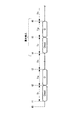
A―2:表示原理
次に、階調表示の原理について説明する。図4は分割セルの構造を簡略化して示した断面図である。この例の電気泳動表示装置にあっては、まず、リセット動作が行われる。このリセット動作では、電気泳動粒子3が画素電極104側に引き寄せられる。正に帯電した電気泳動粒子3を用いる場合、共通電極201の電圧を基準として負極性の電圧が画素電極104に印加される。この結果、図4(A)に示すように電極104に電気泳動粒子3を引き寄せられる。
A-2: Display Principle Next, the principle of gradation display will be described. FIG. 4 is a cross-sectional view showing a simplified structure of the divided cell. In the electrophoretic display device of this example, first, a reset operation is performed. In this reset operation, the
次に、図4(B)に示すように表示すべき階調に応じた正極性の電圧を電極間に印加する。すると、電界によって電気泳動粒子3は共通電極201側に移動する。電位差をゼロにすると、電界が作用しなくなるので、電気泳動粒子3は分散媒2の粘性抵抗によって停止する。この場合、電気泳動粒子3の移動速度は、電界強度、すなわち印加電圧に応じて定まるから、その移動距離は、印加電圧と印加時間に応じて定まることになる。したがって、印加時間を一定にすれば、印加電圧を調整することによって、電気泳動粒子3の厚さ方向の位置を制御できる。
Next, as shown in FIG. 4B, a positive voltage corresponding to the gradation to be displayed is applied between the electrodes. Then, the
共通電極201側から入射した光は電気泳動粒子3によって反射され、この反射光が共通電極201を通過して観測者の目に至る。入射光と反射光は分散媒2によって吸収され、その吸収の程度は光路長に比例する。したがって、観測者が認識する階調は、電気泳動粒子3の位置によって定まることになる。上述したように、印加時間を一定にしたとき電気泳動粒子3の厚さ方向の位置は、印加電圧に応じて定まるから、表示すべき階調応じた電圧を印加すれば、所望の階調表示を得ることができる。
Light incident from the
ところで、分散系1は多数の電気泳動粒子3を含んでいる。ここで、電気的特性(例えば、電荷量)や機械的特性(例えば、粒子径、重量)等の粒子特性が揃っているとすれば、総ての粒子の移動速度が一定となり、総ての電気泳動粒子3は同じようにふるまうことになる。
By the way, the
しかしながら、分割セルの厚さは数μm〜数10μmであり最大移動距離が極めて短いので、階調数を多くしようとすると、微小な移動距離を制御する必要がある。このため、1階調分の印加電圧が極めて小さくなり、階調制御が困難になる。 However, since the thickness of the divided cell is several μm to several tens of μm and the maximum moving distance is extremely short, it is necessary to control a minute moving distance in order to increase the number of gradations. For this reason, the applied voltage for one gradation becomes extremely small, and gradation control becomes difficult.
そこで、本実施形態では、分散系1内に含める多数の電気泳動粒子3の粒子特性にバラツキを持たせてある。粒子特性にバラツキを持たせると、ある電圧を一定時間印加したときの電気泳動粒子3の位置は広がりを持つ。図5は、電極間の電圧と階調濃度との関係の一例を示すグラフである。この例は、50msecの印加時間で、電気泳動粒子3が共通電極201に到達する印加電圧の平均値が5Vであり、到達するのに要する印加電圧の標準偏差が0.2Vである場合をシュミレーションしたものである。
Therefore, in the present embodiment, the particle characteristics of the numerous
同図において、実線は印加電圧に対する階調特性を示しており、点線は印加電圧に対する確率密度を示している。ここで、確率密度とは、共通電極201に到達する電気泳動粒子3の個数を、平均値5Vで正規化したものである。
In the figure, the solid line indicates the gradation characteristics with respect to the applied voltage, and the dotted line indicates the probability density with respect to the applied voltage. Here, the probability density is obtained by normalizing the number of
この図に示すように、印加電圧が4.5V以下の場合には、電気泳動粒子3が殆ど共通電極201に到達しないが、印加電圧が5Vの場合には、半分の電気泳動粒子3が共通電極201に到達しており、さらに印加電圧が5.5V以上の場合には殆どの電気泳動粒子3が共通電極201に到達している。したがって、表示すべき階調に応じて印加電圧値を4.5Vから5.5Vの間で制御すれば、所望の階調表示を行うことが可能となる。
As shown in this figure, when the applied voltage is 4.5V or less, the
A−3:駆動回路
次に、走査線101およびデータ線102を駆動する駆動回路について説明する。まず、図3に示す走査線駆動回路130は、シフトレジスタ(図示略)を有しており、タイミングジェネレータ400からのYクロック信号YCKや、その反転YクロックYCKBに基づいて、垂直走査期間の開始でアクティブとなるY転送開始パルスDYを順次シフトして、走査線信号Y1、Y2、…、Ymを生成する。これにより、図7に示すようにアクティブ期間(Hレベル期間)が順次シフトしていく走査線信号Y1、Y2、…、Ymが生成され、各走査線101に出力される。
A-3: Drive Circuit Next, a drive circuit that drives the
次に、データ線駆動回路140Aについて説明する。図6はデータ線駆動回路140Aのブロック図である。同図に示すようにデータ線駆動回路140Aは、Xシフトレジスタ141、6ビットの画像データDが供給されるバスBUS、スイッチSW1〜SWn、第1ラッチ142、第2ラッチ143、選択回路144、およびD/Aコンバータ145を備えている。
Next, the data
まず、Xシフトレジスタ141は、XクロックXCKおよび反転XクロックXCKBにしたがって、X転送開始パルスDXを順次シフトしてサンプリングパルスSR1、SR2、…、SRn(図7参照)を順次生成するようになっている。
First, the
次に、バスBUSは、スイッチSW1〜SWnを介して第1ラッチ群142の各ラッチに接続されており、スイッチSW1〜SWnの各制御入力端子には、サンプリングパルスSR1、SR2、…、SRnが供給されるようになっている。また、あるスイッチSWjは、6ビットの画像データDに対応して6個で1組の構成となっている。したがって、サンプリングパルスSR1、SR2、…、SRnに各々同期して、画像データDが第1ラッチ142に同時に取りこまれることになる。
Next, the bus BUS is connected to each latch of the
次に、第1ラッチ142は、スイッチSW1〜SWnから供給される画像データDをラッチし、点順次画像データDa1〜Danとして出力する。また、第2ラッチ143は、第1ラッチ142の各点順次画像データDa1〜DanをラッチパルスLATによってラッチする。ここで、ラッチパルスLATは1水平走査期間毎にアクティブとなる信号である。したがって、この第2ラッチ143は、点順次画像データDa1〜Danから線順次画像データDb1〜Dbnを生成する。
Next, the
次に、選択回路144には、画像信号処理回路300Aで生成される共通電圧データDcomとタイミングジェネレータ400で生成される無バイアスタイミング信号Cbとが供給されている。ここで、共通電圧データDcomは共通電極201に給電される電圧値(例えば、接地レベル)を指示するデータである。また、無バイアスタイミング信号Cbは、図7に示すように1水平走査期間中の途中からその終了までの期間においてアクティブ(Hレベル)となる信号である。選択回路144は、無バイアスタイミング信号Cbがアクティブの期間に共通電圧データDcomを選択する一方、これが非アクティブの期間に線順次画像データDb1〜Dbnを選択して図7に示すデータDc1〜Dcnを出力する。
Next, the
D/Aコンバータ145は、6ビットのデータDc1〜Dcnをデジタル信号からアナログ信号に変換して、データ線信号X1〜Xnとして各々生成し、これを各データ線102に供給している。
The D /
A−4:電気泳動表示装置の動作
次に、電気泳動表示装置の動作について説明する。図8は画像信号処理回路300Aの出力データを示すタイミングチャートである。この図を参照しつつ、動作の概要を説明する。
A-4: Operation of Electrophoretic Display Device Next, the operation of the electrophoretic display device will be described. FIG. 8 is a timing chart showing output data of the image
まず、時刻t0において、電気泳動表示装置の電源がオフ状態からオン状態に切り替わると、画像信号処理回路300A、タイミングジェネレータ400および電気泳動表示パネルAに電源が給電される。そして、所定期間が経過し回路動作が安定した時刻t1において、画像信号処理回路300Aは、リセットデータDrestを1フィールド期間出力する。このリセット期間Trにあっては、表示原理で説明したように、電気泳動粒子3が画素電極104側に引き寄せられ、その空間的な状態が初期化される。詳細は後述するが、データ線駆動回路140Aが、リセットデータDrestのデータ値に応じたリセット電圧Vrestを各データ線102に出力する一方、走査線駆動回路130が各走査線101を順次選択することにより、画素電極104に電圧が供給され、すべての画素電極104と共通電極201の間にリセット電圧Vrestが印加されることになる。
First, when the power source of the electrophoretic display device is switched from the off state to the on state at time t0, power is supplied to the image
次に、時刻t2に至ると、書込期間Twが開始する。この書込期間Twにあっては、画像信号処理回路300Aは1フィールド期間にわたって画像データDを出力する。各画素電極104には表示すべき階調に対応した階調電圧Vが書き込まれ、1枚の表示画面が完成することになる。
Next, when the time t2 is reached, the writing period Tw starts. In the writing period Tw, the image
次に、時刻t3から時刻t4までの保持期間Thは、直前の書込期間Twで書き込まれた画像を保持する期間であり、その長さは任意に設定できる。当該期間において、画像信号処理回路300Aは動作を停止しデータを出力せず、また、画素電極104と共通電極201との間には、電界が発生しないようになっている。電気泳動粒子3は、電界がなければ空間的な状態に変化がない。したがって当該期間にあっては、静止画像が表示されることになる。
Next, the holding period Th from time t3 to time t4 is a period for holding the image written in the immediately preceding writing period Tw, and the length thereof can be arbitrarily set. In this period, the image
次に、時刻t4から時刻t6は画像を書き換えるための期間であり、時刻t1から時刻t3までの期間と同様に、リセット動作と書き込み動作が行われる。これにより、表示画面の更新を行うことができる。 Next, the period from time t4 to time t6 is a period for rewriting an image, and a reset operation and a writing operation are performed as in the period from time t1 to time t3. Thereby, the display screen can be updated.
(1)リセット動作
次に、リセット動作について詳細に説明する。図9はリセット動作における電気泳動表示装置のタイミングチャートである。上述したようにリセット期間Trにあっては、リセットデータDrestがデータ線駆動回路140Aに供給される。また、無バイアスタイミング信号Cbは図9に示すように非アクティブ(Lレベル)となるので、データ線信号X1〜Xnの電圧はリセット電圧Vrestとなる。
(1) Reset Operation Next, the reset operation will be described in detail. FIG. 9 is a timing chart of the electrophoretic display device in the reset operation. As described above, during the reset period Tr, the reset data Drest is supplied to the data line driving
この例では、電気泳動粒子3に正電荷が帯電しているので、リセット電圧Vrestは共通電極電圧Vcomを中心として負極性の値を取る。ここで、走査線信号Y1がアクティブ(Hレベル)になると、第1行目のTFT103がオン状態となり、リセット電圧Vrestが各画素電極104に書き込まれる。以後、第2行目、第3行目、…、第m行目の各画素電極104にリセット電圧Vrestが印加される。例えば、時刻txにおいて走査線信号Y1がアクティブから非アクティブに変化すると、第1行目の各TFT103がオフ状態になり、画素電極104とデータ線102とが切断される。しかしながら、画素電極104、分散系1、および共通電極201によって画素容量が形成されているから、TFT103がオフ状態になっても第1行目の画素電極104と共通電極201間ではリセット電圧Vrestが維持される。こうして電極間にリセット電圧Vrestが印加されると、分散系1中の電気泳動粒子3が画素電極104に引き寄せられ、その空間的な状態が初期化される。
In this example, since the
(2)書込動作
次に、書込動作について詳細に説明する。図10は書込動作における電気泳動表示装置のタイミングチャートである。ここでは、i行(i番目の走査線)・j列(j番目のデータ線)の画素における書込動作を説明するが、他の画素においても同様の書き込みがなされることは勿論である。なお、以下の説明では、i行j列の画素をPijと、画素Pijに表示すべき階調を示す階調電圧をVijと、また、画素Pijの輝度をIijと表すことにする。
(2) Write Operation Next, the write operation will be described in detail. FIG. 10 is a timing chart of the electrophoretic display device in the writing operation. Here, the writing operation in the pixels of i row (i th scanning line) and j column (j th data line) will be described, but it goes without saying that the same writing is performed in other pixels. In the following description, the pixel in i row and j column is represented as Pij, the gradation voltage indicating the gradation to be displayed on the pixel Pij is represented as Vij, and the luminance of the pixel Pij is represented as Iij.
各データ線信号X1〜Xnは、図7に示すデータDc1〜DcnをD/A変換して生成されるので、j番目のデータ線102に供給されるデータ線信号Xjの電圧は、図10に示すように、時刻T1から時刻T2まで階調電圧印加期間Tvにおいて階調電圧Vijとなる一方、時刻2から時刻T3までの無バイアス期間Tbにおいて共通電極電圧Vcomとなる。
Since the data line signals X1 to Xn are generated by D / A converting the data Dc1 to Dcn shown in FIG. 7, the voltage of the data line signal Xj supplied to the
また、i番目の走査線101に供給される走査線信号Yiは、i番目の水平走査期間においてアクティブとなり、この間、画素Pijを構成するTFT103はオン状態となる。そして、i番目の水平走査期間のうち時刻T1から時刻T2までの期間は、画素Pijの画素電極104にデータ線信号Xj(すなわち、階調電圧Vij)が印加され、時刻T2から時刻T3までの期間は共通電極電圧Vcomが印加される。
Further, the scanning line signal Yi supplied to the i-
次に、画素Pijにおける電気泳動粒子3の挙動について考察する。この書込動作の前には上述したリセット動作が行われているから、時刻T1において、画素Pijの電気泳動粒子3は画素電極104側に総て位置している。このとき、画素電極104に階調電圧Vijが印加されると、画素電極104から共通電極201へ向けて電界が付与される。したがって、時刻T1から電気泳動粒子3は移動を開始する。
Next, the behavior of the
ここで、i行j列の画素Pijにおける輝度Iijはその画素Pijにおける電気泳動粒子の平均的な移動量により決定される。この例の電気泳動粒子3は白色であり分散媒2は黒色であるから、電気泳動粒子3が共通電極201に近づくほど、画素Pijの輝度Iijは高くなる。したがって、図に示すように輝度Iijは、時刻T1から次第に高くなる。
Here, the luminance Iij in the pixel Pij in the i row and j column is determined by the average amount of movement of the electrophoretic particles in the pixel Pij. Since the
ところで、画素Pijは、画素電極104と共通電極201との間に分散系1を挟持して構成されているので、電極面積、電極間の距離、および分散系1の誘電率に応じた画素容量を有する。
Incidentally, since the pixel Pij is configured by sandwiching the
したがって、TFT103をオフ状態にして画素電極104への電荷の供給を停止したとしても、画素容量には電荷が蓄積されているので、両電極間には一定の電界が継続して発生することになる。電界が付与される限り電気泳動粒子3は共通電極201に向けて泳動を続けるので、電界の発生を停止する期間、換言すれば、画素容量に蓄積されている電荷を取り去る工程が必要となる。無バイアス期間Tbはこのために設けられたものである。
Therefore, even if the supply of charge to the
無バイアス期間Tbにあっては、共通電極電圧Vcomが画素電極104に印加されるので、時刻T2において画素電極104と共通電極201が等電位になる。このため、時刻T2から電気泳動粒子3には電界が作用しなくなる。ここで、分散媒2の粘性抵抗がある程度大きいとすれば、電気泳動粒子3は外力が作用しなくなくなる時刻T2において泳動を停止する。この結果、輝度Iijは図に示すように時刻T2から一定の値を取ることになる。なお、分散媒2の粘性抵抗が小さい場合には電界が作用しなくなっても電気泳動粒子3が惰性で泳動した後に停止するが、そのような場合には、画像信号処理回路300Aにおいて、惰性による泳動を見込んで補正した画像データDを生成するようになっている。
In the no-bias period Tb, the common electrode voltage Vcom is applied to the
この書込動作にあっては、まず、画素Pijの画素電極104に電荷を供給し、電極間に階調電圧Vijを印加し、電気泳動粒子3を表示すべき階調に応じた距離だけ移動させた後、画素電極104に電荷を供給し、共通電極電圧Vcomを印加し、電気泳動粒子3の泳動を停止させるので、画素Pijの輝度Iijを表示すべき階調に応じたものとすることができる。なお、この例では、電気泳動粒子3の泳動を停止させるために共通電極電圧Vcomを印加したが、完全に共通電極電圧Vcomと一致する電圧を印加する必要はなく、電気泳動粒子3の泳動を停止させることができる電圧であればよい。電気泳動粒子3は粘性抵抗に打ち勝たなければ泳動できないので、分散媒2の粘性抵抗などが大きい場合には、印加電圧が共通電極電圧Vcomと多少相違してもよい。
In this writing operation, first, a charge is supplied to the
(3)保持動作
次に、保持動作について説明する。図7において、時刻T3に至ると、全ての走査線信号Yiが非アクティブになるので、全ての画素PijのTFT103はオフ状態となる。上述したように無バイアス期間Tbにおいて画素電極104には共通電極電圧Vcomが印加されるから電極間に電界が発生しないことになる。
(3) Holding Operation Next, the holding operation will be described. In FIG. 7, when the time T3 is reached, all the scanning line signals Yi become inactive, so that the
したがって、新たに画素電極104に電圧を印加しない限り、分散系1には電界が付与されない。この結果、分散系1中の電気泳動粒子3の空間的な状態は保持されることになり、これにより、表示画像の内容を保持することができる。このような保持期間Thにあっては、画素電極104に電圧を印加する必要がないので、走査線信号Y1〜Ymを生成する必要もなければ、データ線信号X1〜Xnを生成する必要もない。このため、当該期間にあっては、以下に述べる各種の方法で消費電力を削減できる。
Therefore, unless a voltage is newly applied to the
第1の方法は、電気泳動表示装置自体の主電源をオフ状態にすることである。これにより、電気泳動表示パネルAや周辺回路たる画像信号処理回路300Aおよびタイミングジェネレータ400は動作を停止することになり、一切電力を消費しないことになる。
The first method is to turn off the main power supply of the electrophoretic display device itself. As a result, the operation of the electrophoretic display panel A, the image
第2の方法は、電気泳動表示パネルAへの給電を停止することである。これにより、電気泳動表示パネルAで消費される電力を削減することができる。 The second method is to stop the power supply to the electrophoretic display panel A. Thereby, the power consumed by the electrophoretic display panel A can be reduced.
第3の方法は、YクロックYCKおよび反転YクロックYCKBと、XクロックXCKおよび反転XクロックXCKBとを、走査線駆動回路130およびデータ線駆動回路140Aへ供給するのを停止することである。上述したように走査線駆動回路130およびデータ線駆動回路140Aは相補型のTFTで構成されているため、電流が流れるときだけ、換言すれば、論理レベルの反転があるときに限り電力を消費する。したがって、クロックの供給を停止することによって消費電力を削減することが可能となる。
A third method is to stop supplying the Y clock YCK and the inverted Y clock YCKB, and the X clock XCK and the inverted X clock XCKB to the scanning
(4)書換動作
次に、表示画面の内容を書き換える書換動作について説明する。書換動作にあっては、以下に述べる各種の態様がある。
(4) Rewriting Operation Next, a rewriting operation for rewriting the contents of the display screen will be described. In the rewriting operation, there are various modes described below.
まず、第1の態様では、上述したリセット動作を行って各行毎に順次初期化を行い、次に、上述した書込動作を行って各行毎に順次、画素電極104に電荷を供給し、階調電圧と共通電極電圧Vcomとを印加する。これにより、画面全体を書き換えることが可能となる。
First, in the first mode, the above-described reset operation is performed to sequentially initialize each row, and then the above-described write operation is performed to sequentially supply charges to the
次に、第2の態様では、書き換えが必要となるラインに限って、リセット動作と書込動作を行う。ここでは、一例として第j番目と第j+1番目のラインを書き換える場合について説明する。図11は第2の態様に係るリセット動作を説明するためのタイミングチャートである。まず、リセット期間Trにあっては、画像信号処理回路300AがリセットデータDrestを出力する。また、当該期間において走査線駆動回路130は、図に示すように走査線信号Y1、…、Yj、Yj+1、…、Ymを順次出力する。
Next, in the second mode, the reset operation and the write operation are performed only on the lines that need to be rewritten. Here, a case where the jth and j + 1th lines are rewritten will be described as an example. FIG. 11 is a timing chart for explaining the reset operation according to the second embodiment. First, in the reset period Tr, the image
一方、無バイアスタイミング信号Cbは、書き換えるべき走査線101を選択する期間にのみLレベルとなる。この例では、j番目とj+1番目のラインを書き換えるので、走査線信号Yj、Yj+1がアクティブとなる期間中に無バイアスタイミング信号CbはLレベル(非アクティブ)となる。上述したように選択回路144(図6参照)は無バイアスタイミング信号CbがHレベル(アクティブ)のときに共通電圧データDcomを出力する一方、その論理レベルがLレベルのときに第2ラッチ143の出力データDb1〜Dbnを出力する。換言すれば、j番目とj+1番目の走査線101を選択する期間にあっては、総てのデータ線102にリセット電圧Vrestが供給される一方、他の走査線101の選択期間にあっては、総てのデータ線102に共通電極電圧Vcomが供給される。
On the other hand, the non-bias timing signal Cb becomes L level only during a period in which the
したがって、図11に示すように第1行〜第j-1行目と第j+2〜第m行の画素電極104には共通電極電圧Vcomが供給される一方、第j行および第j+1行の画素電極104には、リセット電圧Vrestが供給される。したがって、第j行および第j+1行の画素にあっては、電気泳動粒子3の空間的な状態が初期化されることになる。一方、共通電極電圧Vcomが画素電極104に書き込まれても電界は発生しないので、第1行〜第j-1行目と第j+2〜第m行の画素では電気泳動粒子3の空間的な状態は変化しない。次に、書込動作にあっては、画像信号処理回路300Aが書き換えるべきラインについてのみ画像データDを出力し、他のラインについては共通電圧データDcomを出力し、図7に示す通常の書込動作と同様に書き込みを行う。これにより、第j行と第j+1行に限って書き換えを行うことができる。
Therefore, as shown in FIG. 11, the common electrode voltage Vcom is supplied to the
次に、第3の態様では、書き換えるべき複数のラインを同時にリセットして、この後,通常の書込動作によって書き換えを行う。第2の態様では、第j行の次に第j+1行をリセットするといったように、行毎に順次リセット動作を行ったが、書き換えるべき複数の走査線101を同時に選択できる走査線駆動回路を用いれば、同時にリセットを行うことが可能である。例えば、図12に示すように、走査線信号Yj、Yj+1のみを同時にアクティブにして、データ線102にリセット電圧Vrestを供給すれば、図13に示すように書き換えるべきj番目とj+1番目のラインを同時にリセットすることができることは勿論である。また、書込動作にあっては、画像信号処理回路300Aが書き換えるべきラインについてのみ画像データDを出力し、他のラインについては共通電圧データDcomを出力し、図7に示す通常の書込動作と同様に書き込みを行う。これにより、第j行と第j+1行に限って書き換えを行うことができる。
Next, in the third aspect, a plurality of lines to be rewritten are reset at the same time, and then rewritten by a normal writing operation. In the second mode, the reset operation is sequentially performed for each row such that the j + 1th row is reset next to the jth row, but a scanning line driving circuit capable of simultaneously selecting a plurality of
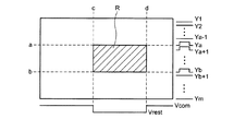
次に、第4の態様では、書き換えるべき領域を同時にリセットして、その後、当該領域の画素電極104に新たな階調電圧を印加する。ここでは、図14に示すように書き換えるべき領域Rが、a番目の行からb番目の行まで、かつ、c番目の列からd番目の列までにある場合を想定する。
Next, in the fourth aspect, the region to be rewritten is reset at the same time, and then a new gradation voltage is applied to the
まず、走査線駆動回路としては、第3の態様と同様に書き換えるべき複数の走査線101を同時に選択できるものを用いる。次に、画像信号処理回路300Aは、1ライン分のデータとして、第1番目から第c-1番目までは共通電圧データDcomを、第c番目から第d番目まではリセットデータDrestを、第d+1番目から第n番目までは共通電圧データDcomを出力する。また、無バイアスタイミング信号Cbは非アクティブとしておく。これにより、所定の水平走査期間において、データ線信号X1〜Xc-1、およびXd+1〜Xnを共通電極電圧Vcomにする一方、データ線信号Xc〜Xdをリセット電圧Vrestにすることができる。そして、当該水平走査期間において、走査線信号Ya〜Ybのみをアクティブとすることにより、領域Rをリセットすることができる。
First, as the scanning line driving circuit, one that can simultaneously select a plurality of
次に、書込動作において、画像信号処理回路300Aは、領域Rに対応する画素電極に画像データDを出力する一方、他の画素電極には共通電圧データDcomを出力する。これにより、領域Rについてのみ書き換えを行うことができる。
次に、第5の態様では総ての画素を同時にリセットして、この後、通常の書込動作を行って書き換えを実行する。図15は、第5の態様に係る電気泳動パネルBのブロック図である。この電気泳動パネルBは、各列毎にTFT105が設けられている点、および走査線駆動回路130Bが総ての走査線信号Y1〜Ymを同時にアクティブとできるようになっている点を除いて、図3に示す電気泳動パネルAと同様に構成されている。
Next, in the writing operation, the image
Next, in the fifth mode, all the pixels are reset at the same time, and thereafter, a normal writing operation is performed to perform rewriting. FIG. 15 is a block diagram of the electrophoresis panel B according to the fifth aspect. The electrophoretic panel B has a
図15において、各TFT105のソース電極にはリセット電圧Vrestが給電され、そのゲート電極にはリセットタイミング信号Crが供給され、さらにそのドレイン電極は各データ線102に接続されている。ここで、リセットタイミング信号Crは、所定のリセット期間Trにおいてのみアクティブとなる信号であり、タイミングジェネレータ400で生成されるようになっている。そして、このリセットタイミング信号Crがアクティブになると、総てのTFT105が同時にオン状態となって、リセット電圧Vrestが各データ線102に供給される。一方、走査線駆動回路130Bは、リセットタイミング信号Crがアクティブになると、総ての走査線信号Y1〜Ymを同時にアクティブにする。したがって、リセットタイミング信号Crのアクティブ期間に、総ての画素電極104にリセット電圧Vrestが印加される。これにより、総ての画素が同時にリセットされる。
In FIG. 15, a reset voltage Vrest is supplied to the source electrode of each
なお、この場合にTFT105の各ソース電極を接地しておき、共通電極電圧Vcomとして接地電位を基準として初期化するのに十分な正極性の電圧を印加するようにしてもよい。すなわち、画素電極104と共通電極201とのうちいずれか一方の電位を基準として、他方の電極に初期化するのに十分な電圧を印加すればよい。なお、共通電極201を分割して複数の分割電極(例えば、上半分と下半分)を設けておき、書き換えるべき画像領域が属する分割電極に初期化するための電圧を印加するようにしてもよい。
In this case, each source electrode of the
B:第2実施形態
上記の実施形態では、画面を書き換える際には、図16(A)に示されるリセット動作を行った後、同図の(B)で示されるような書き込み動作を行い、表示画面を更新していた。この場合、電気泳動粒子3の空間的な状態は一旦初期化される。例えば、分散媒2が黒色に着色されており、電気泳動粒子3が白色であるとすれば、表示を更新する際に、画面全体が暗転(黒)することになる。人の視覚は短時間の変化を検知することができないので、リセット動作に要する期間が短ければ、次々と画面を更新することによって、動画を表示することも可能である。
B: Second Embodiment In the above embodiment, when rewriting the screen, after performing the reset operation shown in FIG. 16A, the write operation shown in FIG. The display screen was updated. In this case, the spatial state of the
しかしながら、分散系1の物理的な性質によっては、リセット動作に長い時間を必要とし、電気泳動粒子3の初期化に伴う輝度変化が検知されることもある。そこで、このような不都合を解消するために、次に表示するべき階調に対応する電気泳動粒子の平均位置と、現在表示中の階調に対応する電気泳動粒子の平均位置との差分に相当する電圧を、両電極間に一定時間、印加しても良い。例えば、現在の階調が50%であり、これを75%の階調に変化させる場合を想定する。図16(B)に示すように電気泳動粒子3の平均的な位置が分散系1の厚さ方向の約1/2にあると、表示階調は50%になる。この階調を75%に変化させるためには、図16(C)に示すように電気泳動粒子3の平均的な位置を厚さ方向に約3/4まで移動させる必要がある。そこで、次に表示すべき階調と現在の階調との差分に応じた電圧を画素電極104に給電して電気泳動粒子3を所定位置まで移動させる。これにより、リセット動作を行うことなく、表示画面の更新が可能となり、動画を容易に表示することができる。
However, depending on the physical properties of the
B−1:画像信号処理回路
次に、画像信号処理回路301Aについて説明する。図17は画像信号処理回路301Aの構成を示すブロック図である。この図に示すように、画像信号処理回路301Aは、A/D変換器310、補正部320、演算部330、選択部340を備えている。外部から供給される画像信号VIDはA/D変換器310を介して入力画像データDinとして補正部320に供給される。補正部320は、ROM等を有しており、入力画像データDinにガンマ補正等の補正処理を施して画像データDvを生成し演算部330に出力する。
B-1: Image Signal Processing Circuit Next, the image
次に、演算部330は、メモリ331と減算器332と備えている。画像データDvは減算器332の一方の入力端子とメモリ331に供給される。メモリ331は、奇数フィールドで書込動作を行う一方、偶数フィールドで読出動作を行う第1フィールドメモリ331Aと、奇数フィールドで読出動作を行う一方、偶数フィールドで書込動作を行う第2フィールドメモリ331Bとを備えている。このメモリ331によって画像データDvは1フィールド遅延され、遅延画像データDv’として減算器332の他方の入力端子に供給される。
Next, the
次に、減算器332は、画像データDvから遅延画像データDv’を減算して差分画像データDdを生成し、これを選択部340に出力する。選択部340は、リセット期間TrにおいてリセットデータDrestを選択する一方、書込期間Twにあっては、差分画像データDdを出力する。なお、最初のフィールドにあっては、遅延画像データDv’が存在しないので、減算器332の他方の入力端子には、データ値が‘0’となるダミーデータが供給されるようになっている。したがって、最初のフィールドでは画像データDvが差分画像データDdとして出力される。
Next, the
ここで、遅延画像データDv’を現在の表示階調とすれば、画像データDvは次に表示すべき階調に相当する。したがって、差分画像データDdは現在の階調と次に表示すべき階調の差分に相当するデータとなる。 Here, if the delayed image data Dv ′ is the current display gradation, the image data Dv corresponds to the gradation to be displayed next. Therefore, the difference image data Dd is data corresponding to the difference between the current gradation and the gradation to be displayed next.
本実施形態の駆動回路およびデータ線回路の構成は第1実施形態と同様のため、説明を省略する。 Since the configuration of the drive circuit and the data line circuit of this embodiment is the same as that of the first embodiment, description thereof is omitted.
B−2:第2実施形態における全体動作
次に、第2実施形態における、電気泳動表示装置の動作について説明する。図18は画像信号処理回路301Aの出力データを示すタイミングチャートである。この図を参照しつつ、動作の概要を説明する。
B-2: Overall Operation in Second Embodiment Next, the operation of the electrophoretic display device in the second embodiment will be described. FIG. 18 is a timing chart showing output data of the image
まず、時刻t0において、電気泳動表示装置の電源がオフ状態からオン状態に切り替わると、画像信号処理回路301A、タイミングジェネレータ400および電気泳動表示パネルAに電源が給電される。そして、所定期間が経過し回路動作が安定した時刻t1において、画像信号処理回路301Aは、リセットデータDrestを1フィールド期間出力する。このリセット期間Trにあっては、表示原理で説明したように、電気泳動粒子3が画素電極104側に引き寄せられ、その空間的な状態が初期化される。詳細は後述するが、データ線駆動回路140Aが、リセットデータDrestのデータ値に応じたリセット電圧Vrestを各データ線102に出力する一方、走査線駆動回路130が各走査線101を順次選択することにより、総ての画素電極104にリセット電圧Vrestが印加される。
First, when the power supply of the electrophoretic display device is switched from the off state to the on state at time t0, the power is supplied to the image
次に、時刻t2に至ると、書込期間Twが開始する。この書込期間Twにあっては、画像信号処理回路301Aは差分画像データDdを出力する。これにより、各画素電極104には表示中の階調と次に表示すべき階調との差に応じた差分階調電圧Vdが書き込まれる。ただし、最初のフィールド(時刻t2から時刻t3まで)にあっては、画像データDvが差分画像データDdとしてデータ線駆動回路140Aに供給されるから、表示すべき階調に応じた電圧が各画素電極104に書き込まれることになる。もっとも、リセット動作によって、表示階調は0%(あるいは100%)になっているから、基本的な機能に着目すれば、最初のフィールドにあっても、表示中の階調と次に表示すべき階調との差分に応じた差分階調電圧Vdを印加しているといえる。
Next, when the time t2 is reached, the writing period Tw starts. In the writing period Tw, the image
このようにして、最初のフィールドで画像が表示されると、次のフィールドでは、差分の階調に対応する電圧が印加され、さらに以後のフィールドでも差分の階調に対応する電圧が印加される。例えば、ある画素に対応する階調電圧Vが、第1フィールドF1から第7フィールドF7までの期間において図19(A)に示すようにv1、v2、…、v7といったように変化するとすれば、差分階調電圧Vdは、同図(B)に示すVd1、Vd2、…、Vd7となる。 In this way, when an image is displayed in the first field, a voltage corresponding to the difference gradation is applied in the next field, and a voltage corresponding to the difference gradation is applied in the subsequent fields. . For example, if the gradation voltage V corresponding to a certain pixel changes in the period from the first field F1 to the seventh field F7 as shown in FIG. 19A, such as v1, v2,. The differential gradation voltage Vd becomes Vd1, Vd2,..., Vd7 shown in FIG.
次に、時刻t5以降の保持期間Thは、直前の書込期間Twで書き込まれた画像を保持する期間であり、その長さは任意に設定できる。当該期間において、画像信号処理回路301Aは動作を停止しデータを出力せず、また、画素電極104と共通電極201との間には、電界が発生しないようになっている。電気泳動粒子3は、電界がなければ空間的な状態に変化がない。したがって当該期間にあっては、静止画像が表示されることになる。
Next, the holding period Th after time t5 is a period for holding the image written in the immediately preceding writing period Tw, and the length thereof can be arbitrarily set. In this period, the image
B−2:書き込み動作
次に、書込動作について詳細に説明する。図20は書込動作における電気泳動表示装置のタイミングチャートである。ここでは、i行(i番目の走査線)・j列(j番目のデータ線)の画素における書込動作を説明するが、他の画素においても同様の書き込みがなされることは勿論である。なお、以下の説明では、i行j列の画素をPijと、画素Pijに表示すべき階調を示す差分階調電圧をVdijと、また、画素Pijの輝度をIijと表すことにする。また、この例では、直前のフィールドにおいて画素Pijは100%の階調レベルを表示したものとする。くわえて、表示階調を0%(総ての電気泳動粒子3が画素電極104側にある)から、100%(総ての電気泳動粒子3が共通電極201側にある)へ変化させる場合に、共通電極電圧Vcomを基準としたときに必要な電圧を+V100、また、表示階調を100%から0%へ変化させる場合に必要な電圧を-V100と表すことにする。
B-2: Write Operation Next, the write operation will be described in detail. FIG. 20 is a timing chart of the electrophoretic display device in the writing operation. Here, the writing operation in the pixels of i row (i th scanning line) and j column (j th data line) will be described, but it goes without saying that the same writing is performed in other pixels. In the following description, a pixel in i row and j column is represented as Pij, a differential gradation voltage indicating a gradation to be displayed on the pixel Pij is represented as Vdij, and a luminance of the pixel Pij is represented as Iij. In this example, it is assumed that the pixel Pij displays a gradation level of 100% in the immediately preceding field. In addition, when the display gradation is changed from 0% (all the
各データ線信号X1〜Xnは、図7(P)〜(R)に示すデータDc1〜DcnをD/A変換して生成されるので、j番目のデータ線102に供給されるデータ線信号Xjの電圧は、図20に示すように、時刻T1から時刻T2までの差分電圧印加期間Tdvにおいて差分階調電圧Vdijとなる。一方、時刻2から時刻T3までの無バイアス期間Tbにおいて共通電極電圧Vcomとなる。ここで、現在のフィールドで表示すべき階調が50%であるとすれば、直前のフィールドの階調と較べて50%減っているので、差分階調電圧Vdijの値は、同図に実線で示すように-V50となる。また、例えば、現在のフィールドで表示すべき階調が0%であるとすれば、同図に一点鎖線で示すように-V100となる。
Since the data line signals X1 to Xn are generated by D / A converting the data Dc1 to Dcn shown in FIGS. 7 (P) to (R), the data line signal Xj supplied to the
C:第3実施形態
次に、第3実施形態に係る電気泳動表示装置について説明する。第1実施形態の電気泳動表示装置にあっては、画素電極104に階調電圧を印加して、表示すべき階調に応じた距離だけ電気泳動粒子3を移動させた後、画素電極104に共通電極電圧Vcomを印加して電気泳動粒子3にクローン力を作用させないようにした。また、分散媒2の粘性抵抗が小さい場合には、共通電極電圧Vcomを印加した後も電気泳動粒子3が惰性で泳動するため、画像信号処理回路300Aにおいて、惰性による泳動を見込んで画像データDを生成していた。
C: Third Embodiment Next, an electrophoretic display device according to a third embodiment will be described. In the electrophoretic display device of the first embodiment, a gradation voltage is applied to the
しかしながら、分散媒2の粘性抵抗の値によっては、電気泳動粒子3の運動をとめさせるのに長時間を要する場合もある。上述した例では電気泳動粒子3が画素電極104から共通電極201に向けて泳動するから、粘性抵抗が極端に小さいと表示画面が次第に明るくなり、やがてある明るさに落ち着くことになる。
However, depending on the value of the viscous resistance of the
第3実施形態は、このような表示画面の明るさの変動を防止できる電気泳動表示装置を提供するものであり、画像信号処理回路300Aの替わりに画像信号処理回路300Bを用いる点、データ線駆動回路140Aの替わりにデータ線駆動回路140Bを用いる点を除いて、図3に示す第1実施形態の電気泳動表示装置と同様に構成されている。
The third embodiment provides an electrophoretic display device that can prevent such fluctuations in the brightness of the display screen, and uses an image
C−1:画像信号処理回路
まず、画像信号処理回路300Bについて説明する。図21は画像信号処理回路300Bのブロック図であり、図22はその出力データのタイミングチャートである。
C-1: Image Signal Processing Circuit First, the image
図21に示すように画像信号処理回路300Bは、A/D変換器310、補正部320、制動電圧データ生成部330、および選択部340を備えている。外部から供給される画像信号VIDはA/D変換器310を介して入力画像データDinとして補正部320に供給される。補正部320は、ROM等を有しており、入力画像データDinにガンマ補正等の補正処理を施して画像データDを生成する。
As illustrated in FIG. 21, the image
制動電圧データ生成部330は、その内部に制動電圧データDsのデータ値を画像データDの取り得るデータ値と対応付けて記憶するテーブルを有しており、画像データDをアドレスとして当該テーブルにアクセスして制動電圧データDsを得るようになっている。なお、テーブルは、RAMやROM等の記憶回路によって構成されている。
The braking voltage
ここで、制動電圧データDsは、後述する制動電圧Vsに対応するものであり、電気泳動粒子3の運動を減衰させるために用いられる。上述したように、分散系1に電界を付与することを停止しても、電気泳動粒子3は惰性による運動を続けるが、この運動の方向と逆向きの力を付与すれば電気泳動粒子3の運動を減衰させその泳動を停止させることができる。電気泳動粒子3は、当初、階調電圧に応じた電界によって泳動しているから、その運動を減衰させるには、第1に逆向きの電界を印加する必要があり、第2にその電界強度は、電気泳動粒子3の運動エネルギー、換言すれば階調電圧Vに応じて定まることになる。そこで、本実施形態にあっては、分散媒2の粘性抵抗等を考慮して、画像データDの値に応じた制動電圧データDsをテーブルに予め記憶しておき読み出すようにしている。
Here, the braking voltage data Ds corresponds to a braking voltage Vs described later, and is used to attenuate the movement of the
次に、選択部340は、図22に示すようにリセット期間TrにおいてはリセットデータDrestを出力する一方、書込期間においては、画像データDと制動電圧データDsを多重した多重データDmを出力する。画像データDが6ビット、制動電圧データDsが6ビットであるとすれば、多重データDmは12ビットのデータであり、MSBから6ビットが画像データD、LSBから6ビットが制動電圧データDsとなる。
Next, as shown in FIG. 22, the
C−2:データ線駆動回路
次に、データ線駆動回路140Bについて説明する。図23はデータ線駆動回路140Bのブロック図である。第2実施形態のデータ線駆動回路140Bは、第1ラッチ142Bおよび第2ラッチ143Bが12ビットのデータをラッチする点、選択回路144の替わりに選択回路144Bを用いる点を除いて、第1実施形態のデータ線駆動回路140Aと同様に構成されている。
C-2: Data Line Drive Circuit Next, the data
第1ラッチ142Bは、12ビットの多重データDmをラッチして点順次画像データDa1〜Danを生成し、第2ラッチ143Bは点順次画像データDa1〜Danを線順次画像データDb1〜Dbnに変換している。もっとも、リセット期間Trに供給されるリセットデータDrestについては、6ビットのままで線順次画像データDb1〜Dbnにしている。
The
次に、図24は、選択回路144Bの詳細な構成を示すブロック図であり、図25はそのタイミングチャートである。図24に示すように選択回路144Bは、n個の選択ユニットU1〜Unを備えており、各選択ユニットU1〜Unは、無バイアスタイミング信号Cbおよび制動タイミング信号Csに基づいて、共通電圧データDcomと多重データDmを構成する画像データDおよび制動電圧データDsとの中から、必要なデータを選択して出力するようになっている。ここで、無バイアスタイミング信号Cbは、上述した第1実施形態と同様に、共通電圧データDcomを選択する期間においてのみアクティブ(Hレベル)となる一方、制動タイミング信号Csは制動電圧データDsを選択する期間にのみアクティブ(Hレベル)となる。
Next, FIG. 24 is a block diagram showing a detailed configuration of the
選択回路144Bは、両信号がともに非アクティブ(Lレベル)のとき、画像データDを選択出力し、さらに制動タイミング信号Csがアクティブのとき制動電圧データDsを選択出力し、くわえて無バイアスタイミング信号Cbがアクティブのとき共通電圧データDcomを選択出力する。
The
例えば、図25に示すように、ある水平走査期間において、i番目の選択ユニットUiにi番目の線順次画像データDbiとして多重データDmiが供給されたとする。この場合、選択回路144Bには、多重データDmiの上位ビットから構成される画像データDiと下位ビットから構成される制動電圧データDsiが供給されることになる。階調電圧印加期間Tvにあっては、制動タイミング信号Csと無バイアスタイミング信号Cbがともに非アクティブであるから、画像データDiが選択され、制動電圧印加期間Tsにあっては制動タイミング信号Csがアクティブとなるから制動電圧データDsiが選択され、さらに、無バイアス期間Tbにあっては、無バイアスタイミング信号Cbがアクティブとなるから共通電圧データDcomが選択されることになる。
For example, as shown in FIG. 25, it is assumed that multiplexed data Dmi is supplied as the i-th line sequential image data Dbi to the i-th selection unit Ui in a certain horizontal scanning period. In this case, the
このようにして選択されたデータは、図23に示すD/Aコンバータ145に供給され、データ線信号X1〜Xnとして各データ線101に出力されることになる。
The data selected in this way is supplied to the D /
C−3:電気泳動表示装置の動作
次に、第3実施形態に係る電気泳動表示装置の動作について説明する。この電気泳動表示装置は、リセット動作→書込動作→保持動作→書換動作(リセット動作および書込動作)といった順に動作する点では、図8を参照して説明した第1実施形態の電気泳動表示装置と同様である。ただし、書込動作(書換動作中のものを含む)中に、画素電極104に電荷を供給し制動電圧を電極間に印加する工程が加えられている点で相違する。以下、相違点である書込動作の詳細について説明する。
C-3: Operation of Electrophoretic Display Device Next, the operation of the electrophoretic display device according to the third embodiment will be described. This electrophoretic display device operates in the order of reset operation → write operation → hold operation → rewrite operation (reset operation and write operation) in the electrophoretic display of the first embodiment described with reference to FIG. It is the same as the device. However, the difference is that a step of supplying a charge to the
図26は書込動作における電気泳動表示装置のタイミングチャートである。ここでは、i行j列の画素Pijにおける書込動作を説明するが、他の画素においても同様の書き込みがなされることは勿論である。 FIG. 26 is a timing chart of the electrophoretic display device in the writing operation. Here, the writing operation in the pixel Pij in the i row and the j column will be described, but it goes without saying that the same writing is performed in the other pixels.
j番目のデータ線102に供給されるデータ線信号Xjの電圧は、図26に示すように、時刻T1から時刻T2まで階調電圧印加期間Tvにおいて階調電圧Vijとなり、時刻T2から時刻T3までの制動電圧印加期間Tsにおいて制動電圧Vsとなり、さらに時刻T3から時刻T4までの無バイアス期間Tbにおいて共通電極電圧Vcomとなる。
As shown in FIG. 26, the voltage of the data line signal Xj supplied to the
また、i番目の走査線101に供給される走査線信号Yiはi番目の水平走査期間においてアクティブとなる。このため、画素Pijを構成するTFT103は当該水平走査期間においてオン状態となり、画素Pijの画素電極104には、時刻T1から時刻T4までのデータ線信号Xjが取り込まれることになる。すなわち、この例ではある走査線のある選択期間において、画素電極104に電荷を供給して、電極間に階調電圧Vijを印加してから、共通電極電圧Vcomを印加するまでの動作が終了する。
Further, the scanning line signal Yi supplied to the i-
次に、画素Pijにおける電気泳動粒子3の挙動について考察する。この書込動作の前にはリセット動作が行われているから、時刻T1において、画素Pijの電気泳動粒子3は画素電極104側に総て位置している。このとき、画素電極104に階調電圧Vijが印加されると、画素電極104から共通電極201へ向けて電界が付与される。したがって、時刻T1から電気泳動粒子3は移動を開始し、輝度Iijは次第に高くなる。
Next, the behavior of the
そして、時刻T2に至ると、画素電極104に制動電圧Vsが印加される。制動電圧Vsの値は、直前に印加される階調電圧Vijの値に応じて設定されており、また、共通電極電圧Vcomを基準として負極性のものである。これは、階調電圧印加期間Tvにおいて、電気泳動粒子3には画素電極104から共通電極201へ向けてのクローン力が作用していたので、これを打ち消す方向に電界を付与する必要があるからである。
Then, at time T2, the braking voltage Vs is applied to the
この制動電圧Vsは、いわばブレーキとして電気泳動粒子3に作用するものであり、運動方向とは逆方向のクローン力を電気泳動粒子3に付与する。これにより、停電圧印加期間Tsの終了時刻T3までに電気泳動粒子3は泳動を停止することとなる。
This braking voltage Vs acts on the
そして、時刻T3に至ると、画素電極104には共通電極電圧Vcomが印加される。すると、画素電極104と共通電極201との電圧が一致して、画素容量に蓄積されていた電荷を放電させることができる。これにより、TFT103をオフ状態にしても画素Pijには電界が全く発生しないことになるので、電気泳動粒子3の空間的な状態を保持することができる。
At time T3, the common electrode voltage Vcom is applied to the
このように本実施形態の書込動作にあっては、まず、画素Pijの画素電極104に階調電圧Vijを印加することにより電気泳動粒子3を移動させ、さらに、制動電圧Vsを印加することによって、電気泳動粒子3の運動を減衰させて停止させるので、分散媒2の粘性抵抗が小さい場合であっても、電気泳動粒子3の惰性による泳動距離を短くすることができる。この結果、輝度の変化がない安定した画像を短時間で表示させることが可能となる。
As described above, in the writing operation of this embodiment, first, the
D:第4実施形態
上記の実施形態においては、階調電圧を印加していたが、その代わりに差分階調電圧を印加しても良い。以下に詳しく説明する。
D: Fourth Embodiment In the above embodiment, the gradation voltage is applied, but a differential gradation voltage may be applied instead. This will be described in detail below.
D−1:画像信号処理回路
まず、画像信号処理回路301Bについて説明する。図27は画像信号処理回路301Bのブロック図であり。
D-1: Image Signal Processing Circuit First, the image
制動電圧データ生成部350は、その内部に制動電圧データDsのデータ値を差分画像データDdの取り得るデータ値と対応付けて記憶するテーブルを有しており、差分画像データDdをアドレスとして当該テーブルにアクセスして制動電圧データDdsを得るようになっている。なお、テーブルは、RAMやROM等の記憶回路によって構成されている。
The braking voltage
ここで、制動電圧データDdsは、後述する制動電圧Vdsに対応するものであり、電気泳動粒子3の運動を減衰させるために用いられる。上述したように、分散系1に電界を付与することを停止しても、電気泳動粒子3は惰性による運動を続けるが、この運動の方向と逆向きの力を付与すれば電気泳動粒子3の運動を減衰させその泳動を停止させることができる。電気泳動粒子3は、当初、差分階調電圧Vdに応じた電界によって与えられるクローン力によって泳動しているから、その運動を減衰させるには、第1に逆向きの電界を印加する必要があり、第2にその電界強度は、電気泳動粒子3の運動エネルギー、換言すれば差分階調電圧Vdに応じて定まることになる。そこで、本実施形態にあっては、分散媒2の粘性抵抗等を考慮して、差分画像データDdの値に応じた制動電圧データDdsをテーブルに予め記憶しておき読み出すようにしている。
Here, the braking voltage data Dds corresponds to a braking voltage Vds described later, and is used to attenuate the movement of the
データ線駆動回路、選択回路は第2実施形態を同様のため、説明を省略する。 Since the data line driving circuit and the selection circuit are the same as those in the second embodiment, description thereof is omitted.
D−2:電気泳動装置の動作
次に、第4実施形態に係る電気泳動表示装置の動作について説明する。
図28は書込動作における電気泳動表示装置のタイミングチャートである。ここでは、i行j列の画素Pijにおける書込動作を説明するが、他の画素においても同様の書き込みがなされることは勿論である。また、この例では、直前のフィールドにおいて画素Pijは100%の階調レベルを表示したものとする。
j番目のデータ線102に供給されるデータ線信号Xjの電圧は、図28に示すように、時刻T1から時刻T2までの差分階調電圧印加期間Tdvにおいて差分階調電圧Vdijとなる。例えば、現在のフィールドで表示すべき階調が50%であるとすれば、直全のフィールドの階調と較べて50%減っているので、差分階調電圧Vdijの値は、同図に実線で示すように-V50となる。また、例えば、現在のフィールドで表示すべき階調が0%であるとすれば、同図に一点鎖線で示すように-V100となる。次に、時刻T2から時刻T3までの制動電圧印加期間Tsにおいてデータ線信号Xjの電圧は制動電圧Vdsijとなる。ここで、制動電圧Vdsijの値は、差分階調電圧Vdijの値に応じて定まる。さらに時刻T3から時刻T4までの無バイアス期間Tdbにおいてデータ線信号Xjの電圧は共通電極電圧Vcomとなる
D-2: Operation of Electrophoretic Device Next, the operation of the electrophoretic display device according to the fourth embodiment will be described.
FIG. 28 is a timing chart of the electrophoretic display device in the writing operation. Here, the writing operation in the pixel Pij in the i row and the j column will be described, but it goes without saying that the same writing is performed in the other pixels. In this example, it is assumed that the pixel Pij displays a gradation level of 100% in the immediately preceding field.
As shown in FIG. 28, the voltage of the data line signal Xj supplied to the
E:第5実施形態
E−1:表示装置
第1実施形態の電気泳動表示装置にあっては、1水平走査期間内に階調電圧印加期間Tvと無バイアス期間Tbを設けて、電気泳動粒子3の移動と停止とを完結させていた。
E: Fifth Embodiment E-1: Display Device In the electrophoretic display device according to the first embodiment, an electrophoretic particle is provided with a gradation voltage application period Tv and a non-bias period Tb within one horizontal scanning period. 3 movement and stop were completed.
これに対して第5実施形態に係る電気泳動表示装置では、フィールド期間単位の階調電圧印加期間Tvfと無バイアス期間Tbfとを設けている。この電気泳動表示装置の構成は、図3に示す第1実施形態と同様であり、無バイアスタイミング信号Cbのアクティブ期間が異なる。 On the other hand, in the electrophoretic display device according to the fifth embodiment, a gradation voltage application period Tvf and a non-bias period Tbf are provided for each field period. The configuration of the electrophoretic display device is the same as that of the first embodiment shown in FIG. 3, and the active period of the biasless timing signal Cb is different.
E−2:全体動作
図29は、電気泳動表示装置の全体動作を示すタイミングチャートである。この図に示すように画像信号処理回路300Aは、リセット期間TrにリセットデータDrestを出力する。当該期間にあっては、電気泳動粒子3が画素電極104側に引き寄せられ、その空間的な状態が初期化される。
E-2: Overall Operation FIG. 29 is a timing chart showing the overall operation of the electrophoretic display device. As shown in this figure, the image
次に、書込期間は1フィールド単位の階調電圧印加期間Tvfと無バイアス期間Tbfとで構成される。階調電圧印加期間Tvfにあっては、画像信号処理回路300Aから出力された画像データDに基づいて、各画素電極104に階調電圧が印加される。ただし、当該期間において無バイアスタイミング信号Cbは非アクティブのままである。したがって、当該期間において共通電極電圧Vcomが各画素電極104に印加されることはない。
Next, the writing period includes a gradation voltage application period Tvf and a non-bias period Tbf in one field unit. In the gradation voltage application period Tvf, a gradation voltage is applied to each
一方、無バイアス期間Tbfにあっては、画像信号処理回路300Aからデータが供給されないが、無バイアスタイミング信号Cbがアクティブとなるので、当該期間にあっては、総てのデータ線102に共通電極電圧Vcomが供給されることになる。したがって、各画素電極104に共通電極電圧Vcomが印加される。すなわち、この例にあっては、ある走査線のある選択期間において、画素電極104に階調電圧Vを印加し、当該走査線が次に選択されるまでの期間、階調電圧Vを保持し、当該走査線の次の選択期間において共通電極電圧Vcomを画素電極104に印加する。
On the other hand, in the no-bias period Tbf, no data is supplied from the image
次に、保持期間Thにあっては、画素電極104と共通電極201との間に、電界を発生させないようになっており、直前の書込期間で書き込まれた画像が保持される。
Next, in the holding period Th, an electric field is not generated between the
そして、書換期間にあっては、最初の画像表示と同様に、リセット→階調電圧の印加→無バイアス(共通電極電圧の印加)といった一連の処理が行われることになる。 In the rewriting period, a series of processes such as reset → application of gradation voltage → no bias (application of common electrode voltage) is performed as in the first image display.
E−3:書き込み動作
図30は書込動作における電気泳動表示装置のタイミングチャートである。ここでは、i行j列の画素Pijにおける書込動作を説明するが、他の画素においても同様の書き込みがなされることは勿論である。
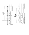
E-3: Write Operation FIG. 30 is a timing chart of the electrophoretic display device in the write operation. Here, the writing operation in the pixel Pij in the i row and the j column will be described, but it goes without saying that the same writing is performed in the other pixels.
j番目のデータ線102に供給されるデータ線信号Xjの電圧は、図30に示すように、階調電圧印加期間Tvfにあっては、1水平走査期間毎に変化する。そして、i番目の水平走査期間においてデータ線信号Xjは階調電圧Vijとなる。このとき、走査線信号Yiがアクティブ(Hレベル)となるから、階調電圧Vijが画素Pijの画素電極104に書き込まれる。これにより、画素電極104の電圧は、時刻T1においてリセット電圧Vrestから階調電圧Vijに遷移して、分散系1に階調に応じた電界が印加されることになる。
As shown in FIG. 30, the voltage of the data line signal Xj supplied to the
また、時刻T2において、走査線信号Yiが非アクティブ(Lレベル)になると、画素PijのTFT103はオフ状態になるが、画素容量には電荷が蓄積されているため、画素電極104の電圧は階調電圧Vijを維持する。
At time T2, when the scanning line signal Yi becomes inactive (L level), the
そして、無バイアス期間Tbfのi番目の水平走査期間において、走査線信号Yiがアクティブになると、共通電極電圧Vcomが画素電極104に印加される。これにより、画素電極104の電圧は、時刻T4に至ると、共通電極電圧Vcomと一致することになる。
In the i-th horizontal scanning period of the non-bias period Tbf, when the scanning line signal Yi becomes active, the common electrode voltage Vcom is applied to the
E−4:電気泳動粒子の挙動
次に、画素Pijにおける電気泳動粒子3の挙動について考察する。この書込動作の前にはリセット動作が行われているから、時刻T0において、画素Pijの電気泳動粒子3は画素電極104側に総て位置している。時刻T1において、画素電極104に階調電圧Vijが印加されると、画素電極104から共通電極201へ向けて電界が付与される。したがって、時刻T1から電気泳動粒子3は移動を開始し、輝度Iijは次第に高くなる。
E-4: Behavior of Electrophoretic Particle Next, the behavior of the
この階調電圧Vijに応じた電界は、時刻T1から時刻T4までの1フィールド期間中印加される。したがって、当該期間において電気泳動粒子3が画素電極104へ向けて移動することになる。すなわち、第1実施形態にあっては、1水平期間中の所定期間に階調電圧Vijを印加したが、第3実施形態では1フィールド期間にわたって階調電圧Vijを印加している。電気泳動粒子3の移動量は、表示原理でも説明したように、分散系1に付与する電界の強さと印加時間に応じて定まる。この例では、1フィールドという長時間に亘って電界を印加するから、弱い電界を印加しても所望の輝度Iijを得ることができる。したがって、本実施形態によればデータ線信号X1〜Xnを低電圧で駆動することが可能となる。
The electric field corresponding to the gradation voltage Vij is applied during one field period from time T1 to time T4. Therefore, the
F:第6実施形態
さらに、上記実施形態においては、階調電圧を印加していたが、それに代わって差分階調電圧を印加しても良い。
F: Sixth Embodiment Further, in the above embodiment, the gradation voltage is applied, but a differential gradation voltage may be applied instead.
F−1:表示装置
図31は、電気泳動表示装置の全体動作を示すタイミングチャートである。この図に示すように画像信号処理回路301Aは、リセット期間TrにリセットデータDrestを出力する。当該期間にあっては、電気泳動粒子3が画素電極104側に引き寄せられ、その空間的な状態が初期化される。
F-1: Display Device FIG. 31 is a timing chart showing the overall operation of the electrophoretic display device. As shown in this figure, the image
次に、書込期間Twは複数の単位期間を備えており、1つの単位期間は1フィールド単位の差分階調電圧印加期間Tdvfと無バイアス期間Tdbfとの組で構成される。差分階調電圧印加期間Tdvfにあっては、画像信号処理回路301Aから出力された差分画像データDdに基づいて、各画素電極104に差分階調電圧Vdが印加される。ただし、当該期間において無バイアスタイミング信号Cbは非アクティブのままである。したがって、当該期間において共通電極電圧Vcomが各画素電極104に印加されることはない。
Next, the writing period Tw includes a plurality of unit periods, and one unit period is composed of a set of a differential gradation voltage application period Tdvf and a non-bias period Tdbf in one field unit. In the difference gradation voltage application period Tdvf, the difference gradation voltage Vd is applied to each
一方、無バイアス期間Tbfにあっては、画像信号処理回路301Aからデータが供給されないが、無バイアスタイミング信号Cbがアクティブとなるので、当該期間にあっては、総てのデータ線102に共通電極電圧Vcomが供給されることになる。したがって、各画素電極104に共通電極電圧Vcomが書き込まれる。すなわち、この例にあっては、ある走査線のある選択期間において、画素電極104に差分階調電圧Vdを印加し、当該走査線が次に選択されるまでの期間、差分階調電圧Vdを保持し、当該走査線の次の選択期間において共通電極電圧Vcomを画素電極104に印加する。
On the other hand, in the no-bias period Tbf, no data is supplied from the image
次に、保持期間Thにあっては、画素電極104と共通電極201との間に、電界を発生させないようになっており、直前の書込期間で書き込まれた画像が保持される。
Next, in the holding period Th, an electric field is not generated between the
F−2:書き込み動作
図32は書込動作における電気泳動表示装置のタイミングチャートである。ここでは、i行j列の画素Pijにおける書込動作を説明するが、他の画素においても同様の書き込みがなされることは勿論である。また、この例では、画素Pijにおける直前の単位期間の階調が10%であり、現在の単位期間で50%の階調を表示させるものとする。
F-2: Write Operation FIG. 32 is a timing chart of the electrophoretic display device in the write operation. Here, the writing operation in the pixel Pij in the i row and the j column will be described, but it goes without saying that the same writing is performed in the other pixels. In this example, the gradation of the unit period immediately before in the pixel Pij is 10%, and 50% gradation is displayed in the current unit period.
j番目のデータ線102に供給されるデータ線信号Xjの電圧は、図32に示すように、差分階調電圧印加期間Tdvfにおいて、1水平走査期間毎に変化する。そして、i番目の水平走査期間においてデータ線信号Xjは差分階調電圧Vdijとなる。このとき、走査線信号Yiがアクティブ(Hレベル)となるから、差分階調電圧Vdijが画素Pijの画素電極104に印加される。これにより、両極間の電圧は、時刻T1において、差分階調電圧Vdijとなり、分散系1に差分階調に応じた電界が印加されることになる。
As shown in FIG. 32, the voltage of the data line signal Xj supplied to the
また、時刻T2において、走査線信号Yiが非アクティブ(Lレベル)になると、画素PijのTFT103はオフ状態になるが、画素容量には電荷が蓄積されているため、電極間の電圧は差分階調電圧Vdijを維持する。
At time T2, when the scanning line signal Yi becomes inactive (L level), the
そして、無バイアス期間Tdbfのi番目の水平走査期間において、走査線信号Yiがアクティブになると、共通電極電圧Vcomが画素電極104に印加される。これにより、画素電極104の電位は、時刻T4に至ると、共通電極電圧Vcomと一致することになる。
In the i-th horizontal scanning period of the non-bias period Tdbf, when the scanning line signal Yi becomes active, the common electrode voltage Vcom is applied to the
G:第7実施形態
G−1:表示装置
第3実施形態の電気泳動表示装置にあっては、1水平走査期間内に階調電圧印加期間Tv、制動電圧印加期間Ts、および無バイアス期間Tbを設けて、電気泳動粒子3の移動と停止とを完結させていた。
G: Seventh Embodiment G-1: Display Device In the electrophoretic display device of the third embodiment, within one horizontal scanning period, the gradation voltage application period Tv, the braking voltage application period Ts, and the no-bias period Tb To complete the movement and stop of the
これに対して第7実施形態に係る電気泳動表示装置では、フィールド単位の階調電圧印加期間Tvf、制動電圧印加期間Tsf、および無バイアス期間Tbfとを設けている。この電気泳動表示装置の構成は、第1実施形態と同様であるが、無バイアスタイミング信号Cbのアクティブ期間が異なる。 On the other hand, in the electrophoretic display device according to the seventh embodiment, a gradation voltage application period Tvf, a braking voltage application period Tsf, and a non-bias period Tbf are provided for each field. The configuration of the electrophoretic display device is the same as that of the first embodiment, but the active period of the biasless timing signal Cb is different.
G−2:全体動作
図33は、電気泳動表示装置の全体動作を示すタイミングチャートである。この図に示すように画像信号処理回路300Aは、リセット期間TrにリセットデータDrestを出力する。当該期間にあっては、電気泳動粒子3が画素電極104側に引き寄せられ、その空間的な状態が初期化される。
G-2: Overall Operation FIG. 33 is a timing chart showing the overall operation of the electrophoretic display device. As shown in this figure, the image
次に、書込期間は1フィールド単位の階調電圧印加期間Tvf、制動電圧印加期間Tsf、および無バイアス期間Tbfとで構成される。階調電圧印加期間Tvfと制動電圧印加期間Tsfとにあっては、画像信号処理回路300Aから出力された画像データDと制動電圧データDsとに基づいて、各画素電極104に階調電圧Vと制動電圧Vsとが各々書き込まれる。ただし、これらの期間において無バイアスタイミング信号Cbは非アクティブのままである。したがって、これらの期間において共通電極電圧Vcomが各画素電極104に印加されることはない。
Next, the writing period includes a gradation voltage application period Tvf, a braking voltage application period Tsf, and a no-bias period Tbf in one field unit. In the gradation voltage application period Tvf and the braking voltage application period Tsf, the gradation voltage V is applied to each
一方、無バイアス期間Tbfにあっては、画像信号処理回路300Aからデータが供給されないが、無バイアスタイミング信号Cbがアクティブとなるので、当該期間にあっては、総てのデータ線102に共通電極電圧Vcomが供給されることになる。したがって、各画素電極104に共通電極電圧Vcomが印加される。すなわち、この例にあっては、ある走査線のある選択期間において、画素電極104に階調電圧Vを書き込み、当該走査線が次に選択されるまでの期間、階調電圧Vを保持し、当該走査線の次の選択期間において画素電極104に制動電圧Vsを印加し、当該走査線がその次に選択されるまでの期間、制動電圧Vsを保持し、当該走査線がその次に選択される期間において共通電極電圧Vcomを画素電極Vcomを印加する。
On the other hand, in the no-bias period Tbf, no data is supplied from the image
次に、保持期間Thにあっては、画素電極104と共通電極201との間に、電界を発生させないようになっており、直前の書込期間で書き込まれた画像が保持される。
Next, in the holding period Th, an electric field is not generated between the
そして、書換期間にあっては、最初の画像表示と同様に、リセット→階調電圧の印加→制動電圧の印加→無バイアス(共通電極電圧の印加)といった一連の処理が行われることになる。 In the rewriting period, as in the first image display, a series of processing such as reset → application of gradation voltage → application of braking voltage → no bias (application of a common electrode voltage) is performed.
G−3:書き込み動作
次に、第4実施形態に係る電気泳動表示装置の書込動作(書換動作中のものを含む)について詳細に説明する。図34は書込動作における電気泳動表示装置のタイミングチャートである。ここでは、i行j列の画素Pijにおける書込動作を説明するが、他の画素においても同様の書き込みがなされることは勿論である。
G-3: Write Operation Next, the write operation (including the rewrite operation) of the electrophoretic display device according to the fourth embodiment will be described in detail. FIG. 34 is a timing chart of the electrophoretic display device in the writing operation. Here, the writing operation in the pixel Pij in the i row and the j column will be described, but it goes without saying that the same writing is performed in the other pixels.
図34に示すように、階調電圧印加期間Tvfのi番目の水平走査期間においてデータ線信号Xjは階調電圧Vijとなる。このとき、走査線信号Yiがアクティブ(Hレベル)となるから、階調電圧Vijが画素Pijの画素電極104に書き込まれる。これにより、画素電極104の電圧は、時刻T1においてリセット電圧Vrestから階調電圧Vijに遷移して、分散系1に階調に応じた電界が印加されることになる。
As shown in FIG. 34, the data line signal Xj becomes the gradation voltage Vij in the i-th horizontal scanning period of the gradation voltage application period Tvf. At this time, since the scanning line signal Yi becomes active (H level), the gradation voltage Vij is written to the
また、時刻T2において、走査線信号Yiが非アクティブ(Lレベル)になると、画素PijのTFT103はオフ状態になるが、画素容量には電荷が蓄積されているため、画素電極104の電圧は階調電圧Vijを維持する。
At time T2, when the scanning line signal Yi becomes inactive (L level), the
次に、制動電圧印加期間Tsfのi番目の水平走査期間において、走査線信号Yiがアクティブになると、階調電圧Vijに応じた制動電圧Vsijが画素電極104に印加される。これにより、画素電極104の電圧は、時刻T4に至ると、制動電圧Vsijと一致することになる。
Next, in the i-th horizontal scanning period of the braking voltage application period Tsf, when the scanning line signal Yi becomes active, the braking voltage Vsij corresponding to the gradation voltage Vij is applied to the
さらに、1フィールド期間が経過すると、無バイアス期間Tbfのi番目の水平走査期間において、走査線信号Yiがアクティブになると、共通電極電圧Vcomが画素電極104に印加される。これにより、画素電極104の電位は、時刻T4に至ると、共通電極電位Vcomと一致することになる。
Further, when one field period elapses, the common electrode voltage Vcom is applied to the
G−4:電気泳動粒子の挙動
次に、画素Pijにおける電気泳動粒子3の挙動について考察する。書込動作前にリセット動作が行われているから、時刻T0において、画素Pijの電気泳動粒子3は画素電極104側に総て位置している。時刻T1において、画素電極104に階調電圧Vijが印加されると、画素電極104から共通電極201へ向けて電界が付与される。したがって、時刻T1から電気泳動粒子3は移動を開始し、輝度Iijは次第に高くなる。
G-4: Behavior of Electrophoretic Particle Next, the behavior of the
次に、時刻T4から時刻T6までの1フィールド期間にあっては、制動電圧Vsijが画素電極に印加される。制動電圧Vsijは共通電極電位Vcomを基準として負極性の電位であるから、共通電極201から画素電極104の向きにクーロン力が作用する。これにより、電気泳動粒子3の運動方向とは逆方向の力を作用させ、電気泳動粒子3の速度を低下させ、時刻T6に至るまでに、その運動を完全に停止させることができる。くわえて、時刻T6から時刻T7の期間には、共通電極電位Vcomが画素電極104に印加されるから、画素容量に蓄積された電荷が放電される。これにより、時刻T7以降、画素PijのTFT103がオフ状態になっても電極間に電界が発生しなくなり、電気泳動粒子3の空間的な状態が保持されることになる。
Next, in one field period from time T4 to time T6, the braking voltage Vsij is applied to the pixel electrode. Since the braking voltage Vsij is a negative potential with respect to the common electrode potential Vcom, a Coulomb force acts in the direction from the
ところで、上述した第2実施形態にあっては、1水平期間中の所定期間に階調電圧Vij、制動電圧Vs、共通電極電圧Vcomを印加するようにしたが、第4実施形態では1フィールド期間にわたって階調電圧Vijおよび制動電圧Vsijを印加している。すなわち、この例では、1フィールドという長時間に亘って階調電圧Vijおよび制動電圧Vsijを印加するから、低い電圧値でも所望の輝度Iijを得ることができる。したがって、本実施形態によればデータ線信号X1〜Xnを低電圧で駆動することが可能となる。 In the second embodiment described above, the gradation voltage Vij, the braking voltage Vs, and the common electrode voltage Vcom are applied in a predetermined period of one horizontal period. In the fourth embodiment, however, one field period is applied. The gradation voltage Vij and the braking voltage Vsij are applied over the entire area. That is, in this example, since the gradation voltage Vij and the braking voltage Vsij are applied for a long time of one field, a desired luminance Iij can be obtained even with a low voltage value. Therefore, according to the present embodiment, the data line signals X1 to Xn can be driven with a low voltage.
H:第8実施形態
さらに、上記第7実施形態においては、階調電圧を印加していたが、これに換えて差分階調電圧を印加することも可能である。
H: Eighth Embodiment Further, in the seventh embodiment, the gradation voltage is applied, but a differential gradation voltage can be applied instead.
H−1:表示装置
図35は、第8実施形態に係る電気泳動表示装置の全体動作を示すタイミングチャートである。この図に示すように画像信号処理回路301Bは、リセット期間TrにリセットデータDrestを出力する。当該期間にあっては、電気泳動粒子3が画素電極104側に引き寄せられ、その空間的な状態が初期化される。
H-1: Display Device FIG. 35 is a timing chart showing the overall operation of the electrophoretic display device according to the eighth embodiment. As shown in this figure, the image
次に、書込期間Twは、複数の単位期間から構成されており、1つの単位期間は、1フィールド単位の差分階調電圧印加期間Tdvf、制動電圧印加期間Tdsf、および無バイアス期間Tdbfで構成される。差分階調電圧印加期間Tdvfと制動電圧印加期間Tdsfとにあっては、画像信号処理回路301Bから出力された差分画像データDdと制動電圧データDdsとに基づいて、各画素電極104に差分階調電圧Vdと制動電圧Vsとが各々印加される。ただし、これらの期間において無バイアスタイミング信号Cbは非アクティブのままである。したがって、これらの期間において共通電極電圧Vcomが各画素電極104に書き込まれることはない。
Next, the writing period Tw is composed of a plurality of unit periods, and one unit period is composed of a differential gradation voltage application period Tdvf, a braking voltage application period Tdsf, and a non-bias period Tdbf in one field unit. Is done. In the difference gradation voltage application period Tdvf and the braking voltage application period Tdsf, a difference gradation is applied to each
一方、無バイアス期間Tbfにあっては、画像信号処理回路301Bからデータが供給されないが、無バイアスタイミング信号Cbがアクティブとなるので、当該期間にあっては、総てのデータ線102に共通電極電圧Vcomが供給されることになる。したがって、各画素電極104に共通電極電圧Vcomが書き込まれる。すなわち、この例にあっては、ある走査線のある選択期間において、画素電極104に差分階調電圧Vdを印加し、当該走査線が次に選択されるまでの期間、差分階調電圧Vdを保持し、当該走査線の次の選択期間において画素電極104に制動電圧Vdsを印加し、当該走査線がその次に選択されるまでの期間、制動電圧Vdsを保持し、当該走査線がその次に選択される期間において共通電極電圧Vcomを画素電極104に印加する。
On the other hand, in the no-bias period Tbf, no data is supplied from the image
次に、保持期間Thにあっては、画素電極104と共通電極201との間に、電界を発生させないようになっており、直前の書込期間Twで書き込まれた画像が保持される。
Next, in the holding period Th, an electric field is not generated between the
H−2:書き込み動作
図36は書込動作における電気泳動表示装置のタイミングチャートである。ここでは、i行j列の画素Pijにおける書込動作を説明するが、他の画素においても同様の書き込みがなされることは勿論である。また、この例では、画素Pijにおける直前の単位期間の階調が10%であり、現在の単位期間で50%の階調を表示させるものとする。 図36に示すように、差分階調電圧印加期間Tdvfのi番目の水平走査期間においてデータ線信号Xjは差分階調電圧Vdijとなる。このとき、走査線信号Yiがアクティブ(Hレベル)となるから、差分階調電圧Vdijが画素Pijの画素電極104に書き込まれる。これにより、画素電極104の電位は、時刻T1において差分階調電圧Vdijに遷移して、分散系1に差分階調に応じた電界が印加されることになる。
H-2: Write Operation FIG. 36 is a timing chart of the electrophoretic display device in the write operation. Here, the writing operation in the pixel Pij in the i row and the j column will be described, but it goes without saying that the same writing is performed in the other pixels. In this example, the gradation of the unit period immediately before in the pixel Pij is 10%, and 50% gradation is displayed in the current unit period. As shown in FIG. 36, the data line signal Xj becomes the differential gradation voltage Vdij in the i-th horizontal scanning period of the differential gradation voltage application period Tdvf. At this time, since the scanning line signal Yi becomes active (H level), the differential gradation voltage Vdij is written to the
また、時刻T2において、走査線信号Yiが非アクティブ(Lレベル)になると、画素PijのTFT103はオフ状態になるが、画素容量には電荷が蓄積されているため、画素電極104の電圧は差分階調電圧Vdijを維持する。
次に、制動電圧印加期間Tsfのi番目の水平走査期間において、走査線信号Yiがアクティブになると、差分階調電圧Vdijに応じた制動電圧Vdsijが画素電極104に印加される。これにより、画素電極104の電圧は、時刻T4に至ると、制動電圧Vdsijと一致することになる。さらに、1フィールド期間が経過すると、無バイアス期間Tdbfのi番目の水平走査期間において、走査線信号Yiがアクティブになる。すると、共通電極電圧Vcomが画素電極104に印加される。
At time T2, when the scanning line signal Yi becomes inactive (L level), the
Next, in the i-th horizontal scanning period of the braking voltage application period Tsf, when the scanning line signal Yi becomes active, the braking voltage Vdsij corresponding to the differential gradation voltage Vdij is applied to the
I:応用例
以上、本発明の一実施形態について説明したが、本発明はこれに限定されるものではなく、その趣旨を逸脱しない範囲で応用・変形が可能であり、例えば、以下に述べる変形が可能である。
I: Application Examples Although one embodiment of the present invention has been described above, the present invention is not limited to this, and can be applied and modified without departing from the spirit thereof. For example, the modifications described below are possible. Is possible.
I−1:動画の表示
上述した各実施形態にあっては、1枚の画像をリセット動作、書込動作の順で形成してこれを保持し、必要に応じて書換動作を行うようにした。したがって、各実施形態の電気泳動表示装置は、静止画を表示するのに適している。しかし、リセット期間Trを短くするとともに、書換動作を周期で繰り返すことによって、動画を表示してもよいことは勿論である。動画を表示する場合には、第1に、電気泳動粒子3に移動速度が速いことが望ましい。このため、分散媒2の粘性抵抗は小さいことが好ましい。このような場合には、分散系1へ電界を付与することを停止しても電気泳動粒子3が惰性で泳動することが多い。したがって、第2実施形態やあるいは第4実施形態で説明したように制動電圧を印加して、電気泳動粒子3の運動を減衰させることが好ましい。
I-1: Display of moving images In each of the above-described embodiments, one image is formed in the order of the reset operation and the writing operation, and this is held, and the rewriting operation is performed as necessary. . Therefore, the electrophoretic display device of each embodiment is suitable for displaying a still image. However, it is a matter of course that a moving image may be displayed by shortening the reset period Tr and repeating the rewrite operation in a cycle. When displaying a moving image, first, it is desirable that the moving speed of the
I−2:リフレッシュ期間
分散系1を構成する分散媒2と電気泳動粒子3の比重は等しいことが好ましいが、素材の制約やバラツキによって両者の比重を完全に一致させることは難しい。このような場合、一旦、画像を書き込んでこれを長時間放置すると、電気泳動粒子3に重力が作用して、粒子が沈降・浮上することがある。そこで、タイミングジェネレータ400の内部に図37に示すタイマー装置を設けて、所定周期で同一画像を再書込みすることが好ましい。
I-2: Refresh Period It is preferable that the specific gravity of the
このタイマー装置410は、タイマー部411と比較部412とを備えている。タイマー部411は、時間か計測して継続時間データDtを生成するとともに、通常の書き込みを指示する書込開始信号Wsと再書込信号Ws’のうちいずれか一方がアクティブになると継続時間データDtの値を‘0’にリセットするようになっている。比較部412は継続時間データDtと予め定められたリフレッシュ期間を指示する基準時間データDrefとを比較して、継続時間データDtと基準時間データDrefを比較して、両者が一致すると、所定時間アクティブとなる再書込信号Ws’を生成するようになっている。
The
図38は、タイマー装置410のタイミングチャートである。この図に示すように書込開始信号Wsがアクティブになると、タイマー部411の継続時間データDtがリセットされ、計測が開始される。そして、予め定められたリフレッシュ期間が経過すると、継続時間データDtと基準時間データDrefとが一致して再書込信号Ws’がアクティブとなる。以後、リフレッシュ期間が経過する毎に再書込信号Ws’がアクティブとなる一方、途中で書込開始信号Wsがアクティブとなれば、その時点からリフレッシュ期間の計測が開始されることなる。このようにして得られた再書込信号Ws’をトリガとして上述した実施形態で説明した書き換え動作(ただし同一画像)を実行することによって、表示画像のリフレッシュを図ることができる
FIG. 38 is a timing chart of the
I−3:電子機器
次に、上述した電気泳動表示装置を用いた電子機器について説明する。
(1)電子書籍
まず、電気泳動表示装置を電子書籍に適用した例について説明する。図39は、この電子書籍を示す斜視図である。図において、電子書籍1000は、電気泳動表示パネル1001、電源スイッチ1002、第1ボタン1003、第2ボタン1004、およびCD−ROMスロット1005を備えている。
I-3: Electronic Device Next, an electronic device using the electrophoretic display device described above will be described.
(1) Electronic book First, an example in which an electrophoretic display device is applied to an electronic book will be described. FIG. 39 is a perspective view showing the electronic book. In the figure, an
利用者が電源スイッチ1002を押して、CD−ROMスロット1005にCD−ROMを装着すると、CD−ROMの内容が読み出され、電気泳動表示パネル1001にメニューが表示される。利用者が第1ボタン1003と第2ボタン1004を操作して、所望の書籍を選択すると電気泳動表示パネル1001に第1頁が表示される。頁を進める場合には第2ボタン1004を押し、頁を戻す場合には第1ボタン1003を押す。
When the user presses the
この電子書籍1000にあっては、書籍の内容を表示した後は、第1ボタン1003および第2ボタン1004を操作したときだけ表示画面を更新する。上述したように電気泳動粒子3は電界が印加されなければ泳動しない。換言すれば、表示画像を維持するためには給電が不要である。このため、表示画面を更新するときだけ、駆動回路に電圧を印加して電気泳動表示パネル1001を駆動している。この結果、液晶表示装置と比較して消費電力を大幅に削減することができる。
In the
また、電気泳動表示パネル1001の表示画像は、顔料粒子である電気泳動粒子3によって表示されるので、表示画面が光ることがない。したがって、電子書籍1000は印刷物と同様の表示が可能であり、これを長時間読んでも目の疲労が少ないといった利点がある。
In addition, since the display image of the
(2)パーソナルコンピュータ
次に、電気泳動表示装置を、モバイル型のパーソナルコンピュータに適用した例について説明する。図40は、このパーソナルコンピュータの構成を示す斜視図である。図において、コンピュータ1200は、キーボード1202を備えた本体部1204と、電気泳動表示パネル1206とから構成されている。この電気泳動表示パネル1206の表示画像は、顔料粒子である電気泳動粒子3によって表示されるので、透過型・半透過型の液晶表示装置で必要とされるバックライトが不要である。このため、コンピュータ1200を小型軽量化することができ、しかも、その消費電力を大幅に削減することが可能である。
(2) Personal Computer Next, an example in which the electrophoretic display device is applied to a mobile personal computer will be described. FIG. 40 is a perspective view showing the configuration of this personal computer. In the figure, a
(3)携帯電話
さらに、電気泳動表示装置を、携帯電話に適用した例について説明する。図41は、この携帯電話の構成を示す斜視図である。図において、携帯電話1300は、複数の操作ボタン1302のほか、受話口1304、送話口1306とともに、電気泳動表示パネル1308を備えるものである。液晶表示装置にあっては偏光板が必要であり、これにより表示画面が暗くなっていたが、電気泳動表示パネル1308は偏光板が不要である。このため、携帯電話1300は明るくて見やすい画面を表示することができる。
(3) Mobile phone Further, an example in which the electrophoretic display device is applied to a mobile phone will be described. FIG. 41 is a perspective view showing the configuration of this mobile phone. In the figure, a
なお、電子機器としては、図39〜図41を参照して説明した他にも、テレビジョンモニタや、屋外の広告板、道路標識、ビューファインダ型、モニタ直視型のビデオテープレコーダ、カーナビゲーション装置、ページャ、電子手帳、電卓、ワードプロセッサ、ワークステーション、テレビ電話、POS端末、タッチパネルを備えた機器等などが挙げられる。そして、これらの各種電子機器に対して、各実施形態の電気泳動表示パネル、さらにはこれを備えた電気光学装置が適用可能なのは言うまでもない。 In addition to the electronic devices described with reference to FIGS. 39 to 41, the electronic device includes a television monitor, an outdoor advertising board, a road sign, a viewfinder type, a monitor direct view type video tape recorder, and a car navigation device. , Pagers, electronic notebooks, calculators, word processors, workstations, videophones, POS terminals, devices equipped with touch panels, and the like. In addition, it goes without saying that the electrophoretic display panel of each embodiment and the electro-optical device including the same can be applied to these various electronic devices.
1……分散系
2……分散媒
3……電気泳動粒子
A……電気泳動表示パネル
101……走査線
102……データ線
103……TFT(スイッチング素子)
104……画素電極
201……共通電極
Vij……階調電圧
Vdij……差分階調電圧
Vs……制動電圧
Y1〜Ym……走査線信号
X1〜Xn……データ線信号
130……走査線駆動回路(走査線駆動部)
140A,140B……データ線駆動回路(データ線駆動部)
DESCRIPTION OF
104 ...
140A, 140B: Data line driving circuit (data line driving unit)
Claims (16)
前記第1の電極と前記第2の電極との間に配置された、電気泳動粒子を含有する分散系と、
複数の走査線と、
前記複数の走査線と交差する複数のデータ線と、
前記データ線と前記走査線との交差に対応して設けられ、前記データ線、前記走査線、及び前記第1の電極に電気的に接続されたスイッチング素子と、
を備えた電気泳動表示装置の駆動方法であって、
表示階調に対応した位置へ前記電気泳動粒子を移動させるために、前記表示階調に対応した値の第1の電圧を、前記第1の電極および前記第2の電極の間に印加するステップと、
前記第1の電極および前記第2の電極の間の電圧を、前記電気泳動粒子が泳動しない第2の電圧とするステップと
を有することを特徴とする電気泳動表示装置の駆動方法。 A first electrode and a second electrode;
A dispersion containing electrophoretic particles disposed between the first electrode and the second electrode;
A plurality of scan lines;
A plurality of data lines intersecting the plurality of scanning lines;
A switching element provided corresponding to the intersection of the data line and the scanning line, and electrically connected to the data line, the scanning line, and the first electrode;
A method for driving an electrophoretic display device comprising:
To move the electrophoretic particles to that corresponding to the display gray scale position, the step of the first voltage value corresponding to the display gradation is applied between the first electrode and the second electrode When,
A method for driving an electrophoretic display device , comprising: setting a voltage between the first electrode and the second electrode to a second voltage at which the electrophoretic particles do not migrate.
前記第1の電圧を印加するステップは、
1水平走査期間にわたって前記走査線に選択電圧を供給することにより前記スイッチング素子をオン状態とし、前記データ線と前記第1の電極とを接続するステップと、
前記スイッチング素子がオン状態となった前記水平走査期間のうち少なくとも一部の期間において、前記第1の電極と前記第2の電極との間に前記第1の電圧を生じさせるための信号を、前記データ線及び前記スイッチング素子を介して前記第1の電極に供給するステップと、
を有することを特徴とする電気泳動表示装置の駆動方法。 A method for driving an electrophoretic display device according to claim 1,
Applying the first voltage comprises:
Supplying a selection voltage to the scanning line over one horizontal scanning period to turn on the switching element, and connecting the data line and the first electrode;
A signal for generating the first voltage between the first electrode and the second electrode in at least a part of the horizontal scanning period in which the switching element is turned on, Supplying to the first electrode via the data line and the switching element ;
A method for driving an electrophoretic display device, comprising:
前記スイッチング素子がオン状態となった前記水平走査期間において、前記一部の期間の後に、前記第1の電極と前記第2の電極との間の電圧が前記第2の電圧となるような信号を、前記データ線及び前記スイッチング素子を介して前記第1の電極に供給することを特徴とする電気泳動表示装置の駆動方法。 A method for driving an electrophoretic display device according to claim 2,
In the horizontal scanning period in which the switching element is turned on, a signal that causes the voltage between the first electrode and the second electrode to become the second voltage after the partial period. Is supplied to the first electrode through the data line and the switching element.
前記第1の電圧を印加するステップは、
第1の水平走査期間において前記走査線に選択電圧を供給することにより前記スイッチング素子をオン状態とし、前記データ線と前記第1の電極とを接続するステップと、
前記第1の水平走査期間において、前記第1の電極と前記第2の電極との間に前記第1の電圧を生じさせるための信号を、前記データ線及び前記スイッチング素子を介して前記第1の電極に供給するステップと
を有し、
前記第1の電極および前記第2の電極の間の電圧を前記第2の電圧とするステップは、
第1の水平走査期間より後の第2の水平走査期間において前記走査線に選択電圧を供給することにより前記スイッチング素子をオン状態とし、前記データ線と前記第1の電極とを接続するステップと、
前記第2の水平走査期間において、前記第1の電極と前記第2の電極との間の電圧が前記第2の電圧となるような信号を、前記データ線及び前記スイッチング素子を介して前記第1の電極に供給するステップと
を有することを特徴とする電気泳動表示装置の駆動方法。 A method for driving an electrophoretic display device according to claim 1,
Applying the first voltage comprises:
Supplying a selection voltage to the scanning line in a first horizontal scanning period to turn on the switching element, and connecting the data line and the first electrode;
In the first horizontal scanning period, a signal for generating the first voltage is generated between the first electrode and the second electrode via the data line and the switching element. Supplying to the electrodes of the
Have
The step of setting the voltage between the first electrode and the second electrode as the second voltage is as follows:
Supplying a selection voltage to the scanning line in a second horizontal scanning period after the first horizontal scanning period to turn on the switching element, and connecting the data line and the first electrode; ,
In the second horizontal scanning period, a signal such that a voltage between the first electrode and the second electrode becomes the second voltage is transmitted through the data line and the switching element. Supplying to one electrode ;
A method for driving an electrophoretic display device, comprising:
前記第1の水平走査期間は、第1のフィールド期間に含まれ、前記第2の水平走査期間
は、前記第1のフィールド期間より後の第2のフィールド期間に含まれることを特徴とする電気泳動表示装置の駆動方法。 A method for driving an electrophoretic display device according to claim 4,
The first horizontal scanning period is included in a first field period, and the second horizontal scanning period is included in a second field period after the first field period. Driving method of electrophoretic display device.
前記第1の電圧を印加するステップの前に、前記第1の電極および前記第2の電極の間にリセット電圧を印加することにより、前記電気泳動粒子を、前記分散系中において前記第1電極側または前記第2電極側へ引き寄せるリセットステップをさらに有することを特徴とする電気泳動表示装置の駆動方法。 A method for driving an electrophoretic display device according to any one of claims 1 to 5,
By applying a reset voltage between the first electrode and the second electrode before applying the first voltage, the electrophoretic particles are moved into the first electrode in the dispersion system. A driving method of an electrophoretic display device, further comprising a reset step of drawing toward the side or the second electrode side.
前記第1の電極と前記第2の電極との間に配置された、電気泳動粒子を含有する分散系と、
複数の走査線と、
前記複数の走査線と交差する複数のデータ線と、
前記データ線と前記走査線との交差に対応して設けられ、前記データ線、前記走査線、及び前記第1の電極に電気的に接続されたスイッチング素子と、
を有する電気泳動表示装置の駆動回路であって、
表示階調に対応した位置へ前記電気泳動粒子を移動させるために、前記第1の電圧を、前記第1の電極および前記第2の電極の間に印加し、
前記第1の電圧を印加した後に、前記第1の電極および前記第2の電極の間の電圧を、前記電気泳動粒子が泳動しない第2の電圧とすることを特徴とする電気泳動表示装置の駆動回路。 A first electrode and a second electrode;
A dispersion containing electrophoretic particles disposed between the first electrode and the second electrode;
A plurality of scan lines;
A plurality of data lines intersecting the plurality of scanning lines;
A switching element provided corresponding to the intersection of the data line and the scanning line, and electrically connected to the data line, the scanning line, and the first electrode;
A drive circuit for an electrophoretic display device comprising:
In order to move the electrophoretic particles to a position corresponding to a display gradation, the first voltage is applied between the first electrode and the second electrode ,
An electrophoretic display device characterized in that after applying the first voltage, the voltage between the first electrode and the second electrode is a second voltage at which the electrophoretic particles do not migrate. Driving circuit.
1水平走査期間にわたって前記走査線に選択電圧を供給することにより前記スイッチング素子をオン状態とし、前記データ線と前記第1の電極とを接続する走査線駆動部と、
前記スイッチング素子がオン状態となった前記水平走査期間のうち少なくとも一部の期間において、前記第1の電極と前記第2の電極との間に前記第1の電圧を生じさせるための信号を、前記データ線及び前記スイッチング素子を介して前記第1の電極に供給するデータ線駆動部と、を有することを特徴とする電気泳動表示装置の駆動回路。 A drive circuit for an electrophoretic display device according to claim 7,
A scanning line driving unit that turns on the switching element by supplying a selection voltage to the scanning line over one horizontal scanning period, and connects the data line and the first electrode;
A signal for generating the first voltage between the first electrode and the second electrode in at least a part of the horizontal scanning period in which the switching element is turned on, A drive circuit for an electrophoretic display device, comprising: a data line drive unit that supplies the first electrode through the data line and the switching element.
前記複数の走査線を駆動する走査線駆動部と、
前記複数のデータ線を駆動するデータ線駆動部と、を有し、
前記走査線駆動部は、第1の水平走査期間において前記走査線に選択電圧を供給することにより前記スイッチング素子をオン状態とし、前記データ線と前記第1の電極とを接続し、
前記データ線駆動部は、前記第1の水平走査期間において、前記第1の電極と前記第2の電極との間に前記第1の電圧を生じさせるための信号を、前記データ線及び前記スイッチング素子を介して前記第1の電極に供給し、
前記走査線駆動部は、前記第1の水平走査期間より後の第2の水平走査期間において前記走査線に選択電圧を供給することにより前記スイッチング素子をオン状態とし、前記データ線と前記第1の電極とを接続し、
前記データ線駆動部は、前記第2の水平走査期間において、前記第1の電極と前記第2の電極との間の電圧が前記第2の電圧となるような信号を、前記データ線及び前記スイッチング素子を介して前記第1の電極に供給することを特徴とする電気泳動表示装置の駆動回路。 A drive circuit for an electrophoretic display device according to claim 7,
A scanning line driving unit for driving the plurality of scanning lines;
A data line driving unit that drives the plurality of data lines,
The scanning line driving unit turns on the switching element by supplying a selection voltage to the scanning line in a first horizontal scanning period, and connects the data line and the first electrode.
The data line driving unit outputs a signal for generating the first voltage between the first electrode and the second electrode in the first horizontal scanning period, and outputs the signal for generating the first voltage. Supplying the first electrode via an element;
The scanning line driving unit turns on the switching element by supplying a selection voltage to the scanning line in a second horizontal scanning period after the first horizontal scanning period, so that the data line and the first line are turned on. Connect with the electrode of
In the second horizontal scanning period, the data line driving unit outputs a signal such that a voltage between the first electrode and the second electrode becomes the second voltage, and the data line and the data line A driving circuit for an electrophoretic display device, wherein the driving circuit supplies the first electrode through a switching element.
前記第1の電極と前記第2の電極との間に配置された、電気泳動粒子を含有する分散系
と、
複数の走査線と、
前記複数の走査線と交差する複数のデータ線と、
前記データ線と前記走査線との交差に対応して設けられ、前記データ線、前記走査線、
及び前記第1の電極に電気的に接続されたスイッチング素子と、
を備え、
表示階調に対応した位置へ前記電気泳動粒子を移動させるために、前記表示階調に対応した値の第1の電圧が、前記第1の電極および前記第2の電極の間に印加され、
前記第1の電圧が印加された後に、前記第1の電極および前記第2の電極の間の電圧が、前記電気泳動粒子が泳動しない第2の電圧とされることを特徴とする電気泳動表示装置。 A first electrode and a second electrode;
A dispersion containing electrophoretic particles disposed between the first electrode and the second electrode;
A plurality of scan lines;
A plurality of data lines intersecting the plurality of scanning lines;
Provided corresponding to the intersection of the data line and the scanning line, the data line, the scanning line,
And a switching element electrically connected to the first electrode;
With
In order to move the electrophoretic particles to a position corresponding to a display gradation, a first voltage having a value corresponding to the display gradation is applied between the first electrode and the second electrode ,
The electrophoretic display characterized in that after the first voltage is applied, the voltage between the first electrode and the second electrode is a second voltage at which the electrophoretic particles do not migrate. apparatus.
1水平走査期間にわたって前記走査線に選択電圧が供給されることにより前記スイッチング素子がオン状態となって前記データ線と前記第1の電極とが接続され、
前記スイッチング素子がオン状態となった前記水平走査期間のうち少なくとも一部の期間において、前記第1の電極と前記第2の電極との間に前記第1の電圧を生じさせるための信号が、前記データ線及び前記スイッチング素子を介して前記第1の電極に供給されることを特徴とする電気泳動表示装置。 The electrophoretic display device according to claim 10,
By supplying a selection voltage to the scanning line over one horizontal scanning period, the switching element is turned on, and the data line and the first electrode are connected,
A signal for generating the first voltage between the first electrode and the second electrode in at least a part of the horizontal scanning period in which the switching element is turned on, The electrophoretic display device, wherein the electrophoretic display device is supplied to the first electrode through the data line and the switching element.
前記スイッチング素子がオン状態となった前記水平走査期間において、前記一部の期間の後に、前記第1の電極と前記第2の電極との間の電圧が前記第2の電圧となるような信号が、前記データ線及び前記スイッチング素子を介して前記第1の電極に供給されることを特徴とする電気泳動表示装置。 The electrophoretic display device according to claim 11,
In the horizontal scanning period in which the switching element is turned on, a signal that causes the voltage between the first electrode and the second electrode to become the second voltage after the partial period. Is supplied to the first electrode through the data line and the switching element.
第1の水平走査期間において前記走査線に選択電圧が供給されることにより前記スイッチング素子がオン状態となって前記データ線と前記第1の電極とが接続され、
前記第1の水平走査期間において、前記第1の電極と前記第2の電極との間に前記第1の電圧を生じさせるための信号が、前記データ線及び前記スイッチング素子を介して前記第1の電極に供給され、
前記第1の水平走査期間より後の第2の水平走査期間において前記走査線に選択電圧が供給されて前記スイッチング素子がオン状態となって前記データ線と前記第1の電極とが接続され、
前記第2の水平走査期間において、前記第1の電極と前記第2の電極との間の電圧が前記第2の電圧となるような信号が、前記データ線及び前記スイッチング素子を介して前記第1の電極に供給されることを特徴とする電気泳動表示装置。 The electrophoretic display device according to claim 10,
By supplying a selection voltage to the scanning line in the first horizontal scanning period, the switching element is turned on, and the data line and the first electrode are connected,
In the first horizontal scanning period, a signal for generating the first voltage is generated between the first electrode and the second electrode via the data line and the switching element. Supplied to the electrode
In a second horizontal scanning period after the first horizontal scanning period, a selection voltage is supplied to the scanning line, the switching element is turned on, and the data line and the first electrode are connected,
In the second horizontal scanning period, a signal such that a voltage between the first electrode and the second electrode becomes the second voltage is transmitted through the data line and the switching element. An electrophoretic display device, wherein the electrophoretic display device is supplied to one electrode.
前記第1の水平走査期間は、第1のフィールド期間に含まれ、前記第2の水平走査期間は、前記第1のフィールド期間より後の第2のフィールド期間に含まれることを特徴とする電気泳動表示装置。 The electrophoretic display device according to claim 13,
The first horizontal scanning period is included in a first field period, and the second horizontal scanning period is included in a second field period after the first field period. Electrophoretic display device.
前記第1の電圧が印加される前に、前記第1の電極および前記第2の電極の間にリセット電圧が印加されることにより、前記電気泳動粒子が、前記分散系中において前記第1電極側または前記第2電極側へ引き寄せられることを特徴とする電気泳動表示装置。 The electrophoretic display device according to any one of claims 10 to 14,
Before the first voltage is applied, by the reset voltage is applied between the first electrode and the second electrode, the electrophoretic particles, the first electrode during the dispersion The electrophoretic display device is drawn to the side or the second electrode side.
Priority Applications (1)
| Application Number | Priority Date | Filing Date | Title |
|---|---|---|---|
| JP2005209302A JP4613727B2 (en) | 2000-06-22 | 2005-07-19 | Electrophoretic display device driving method, driving circuit, electrophoretic display device, and electronic apparatus |
Applications Claiming Priority (3)
| Application Number | Priority Date | Filing Date | Title |
|---|---|---|---|
| JP2000187922 | 2000-06-22 | ||
| JP2000236197 | 2000-08-03 | ||
| JP2005209302A JP4613727B2 (en) | 2000-06-22 | 2005-07-19 | Electrophoretic display device driving method, driving circuit, electrophoretic display device, and electronic apparatus |
Related Parent Applications (1)
| Application Number | Title | Priority Date | Filing Date |
|---|---|---|---|
| JP2001187279A Division JP3750566B2 (en) | 2000-06-22 | 2001-06-20 | Electrophoretic display device driving method, driving circuit, electrophoretic display device, and electronic apparatus |
Related Child Applications (3)
| Application Number | Title | Priority Date | Filing Date |
|---|---|---|---|
| JP2008216246A Division JP4557068B2 (en) | 2000-06-22 | 2008-08-26 | Electrophoretic display device driving method, driving circuit, electrophoretic display device, and electronic apparatus |
| JP2008290705A Division JP4557076B2 (en) | 2000-06-22 | 2008-11-13 | Electrophoretic display device driving method, electrophoretic display device, and electronic apparatus |
| JP2009036205A Division JP4557083B2 (en) | 2000-06-22 | 2009-02-19 | Electrophoretic display device driving method, driving circuit, electrophoretic display device, and electronic apparatus |
Publications (3)
| Publication Number | Publication Date |
|---|---|
| JP2006023757A JP2006023757A (en) | 2006-01-26 |
| JP2006023757A5 JP2006023757A5 (en) | 2009-05-28 |
| JP4613727B2 true JP4613727B2 (en) | 2011-01-19 |
Family
ID=35797015
Family Applications (1)
| Application Number | Title | Priority Date | Filing Date |
|---|---|---|---|
| JP2005209302A Expired - Lifetime JP4613727B2 (en) | 2000-06-22 | 2005-07-19 | Electrophoretic display device driving method, driving circuit, electrophoretic display device, and electronic apparatus |
Country Status (1)
| Country | Link |
|---|---|
| JP (1) | JP4613727B2 (en) |
Cited By (1)
| Publication number | Priority date | Publication date | Assignee | Title |
|---|---|---|---|---|
| JP2013140391A (en) * | 2000-06-22 | 2013-07-18 | Seiko Epson Corp | Control method of electrophoretic display device, control device of electrophoretic display device, electrophoretic display device, and electronic apparatus |
Families Citing this family (8)
| Publication number | Priority date | Publication date | Assignee | Title |
|---|---|---|---|---|
| JP5348363B2 (en) | 2006-04-25 | 2013-11-20 | セイコーエプソン株式会社 | Electrophoretic display device, electrophoretic display device driving method, and electronic apparatus |
| KR101499240B1 (en) | 2006-12-12 | 2015-03-05 | 삼성디스플레이 주식회사 | Method for driving electrophoretic display |
| KR101344272B1 (en) | 2007-04-18 | 2013-12-23 | 삼성디스플레이 주식회사 | Method for driving electro-phoretic display panel |
| KR101383716B1 (en) | 2007-08-17 | 2014-04-10 | 삼성디스플레이 주식회사 | Device and method for driving electrophoretic display |
| KR101427577B1 (en) | 2007-09-06 | 2014-08-08 | 삼성디스플레이 주식회사 | Electrophoretic display and driving method of the same |
| JP5163182B2 (en) * | 2008-02-27 | 2013-03-13 | セイコーエプソン株式会社 | Image rewriting control device and information display device |
| JP5256504B2 (en) * | 2009-11-11 | 2013-08-07 | コニカミノルタ株式会社 | Electronic information display device |
| TWI484275B (en) * | 2010-05-21 | 2015-05-11 | E Ink Corp | Electro-optic display, method for driving the same and microcavity electrophoretic display |
Citations (3)
| Publication number | Priority date | Publication date | Assignee | Title |
|---|---|---|---|---|
| JPH09504618A (en) * | 1993-08-26 | 1997-05-06 | コピイテル,インコーポレイテッド | Electrophoretic display device with short writing time |
| JP2000035775A (en) * | 1998-07-17 | 2000-02-02 | Nok Corp | Electrophoresis display device |
| WO2001091096A1 (en) * | 2000-05-26 | 2001-11-29 | Seiko Epson Corporation | Display and recorded medium |
Family Cites Families (4)
| Publication number | Priority date | Publication date | Assignee | Title |
|---|---|---|---|---|
| JPS51112360A (en) * | 1974-03-25 | 1976-10-04 | Fuji Denko Kk | Display equipment of electrophoresis |
| JPS5327151B2 (en) * | 1974-10-05 | 1978-08-07 | ||
| NL8502663A (en) * | 1985-09-30 | 1987-04-16 | Philips Nv | DISPLAY DEVICE WITH IMPROVED CONTROL. |
| JPH11265167A (en) * | 1998-01-23 | 1999-09-28 | Eastman Kodak Co | Non-radiative color display |
-
2005
- 2005-07-19 JP JP2005209302A patent/JP4613727B2/en not_active Expired - Lifetime
Patent Citations (3)
| Publication number | Priority date | Publication date | Assignee | Title |
|---|---|---|---|---|
| JPH09504618A (en) * | 1993-08-26 | 1997-05-06 | コピイテル,インコーポレイテッド | Electrophoretic display device with short writing time |
| JP2000035775A (en) * | 1998-07-17 | 2000-02-02 | Nok Corp | Electrophoresis display device |
| WO2001091096A1 (en) * | 2000-05-26 | 2001-11-29 | Seiko Epson Corporation | Display and recorded medium |
Cited By (2)
| Publication number | Priority date | Publication date | Assignee | Title |
|---|---|---|---|---|
| JP2013140391A (en) * | 2000-06-22 | 2013-07-18 | Seiko Epson Corp | Control method of electrophoretic display device, control device of electrophoretic display device, electrophoretic display device, and electronic apparatus |
| JP2013167885A (en) * | 2000-06-22 | 2013-08-29 | Seiko Epson Corp | Control method of electrophoretic display device, control device of electrophoretic display device, electrophoretic display device and electronic apparatus |
Also Published As
| Publication number | Publication date |
|---|---|
| JP2006023757A (en) | 2006-01-26 |
Similar Documents
| Publication | Publication Date | Title |
|---|---|---|
| JP3750566B2 (en) | Electrophoretic display device driving method, driving circuit, electrophoretic display device, and electronic apparatus | |
| JP3750565B2 (en) | Electrophoretic display device driving method, driving circuit, and electronic apparatus | |
| JP4613727B2 (en) | Electrophoretic display device driving method, driving circuit, electrophoretic display device, and electronic apparatus | |
| JP4557083B2 (en) | Electrophoretic display device driving method, driving circuit, electrophoretic display device, and electronic apparatus | |
| JP4618031B2 (en) | Electrophoretic display device driving method, driving circuit, electrophoretic display device, and electronic apparatus | |
| JP5045976B2 (en) | Electrophoretic display device and driving method thereof | |
| KR20070105279A (en) | Electrophoresis display device, method of driving electrophoresis display device, and electronic apparatus | |
| JP4013550B2 (en) | Electro-optical device driving method, driving circuit, electro-optical device, and electronic apparatus | |
| JP3613180B2 (en) | Electro-optical device driving method, driving circuit, electro-optical device, and electronic apparatus | |
| JP2003022058A (en) | Electrooptic device, driving circuit for electrooptic device, driving method for electrooptic device, and electronic equipment | |
| JP2004094168A (en) | Electro-optical device, method for driving electro-optical device and electronic appliance | |
| JP5668771B2 (en) | Control method for electrophoretic display device, control device for electrophoretic display device, electrophoretic display device, and electronic apparatus | |
| JP4269605B2 (en) | Dispersion system drive circuit drive method and electrophoretic display device drive method | |
| JP2009109705A (en) | Electro-optical device, driving method for electro-optical device, and electronic equipment | |
| JP2011013420A (en) | Electro-optical device, method for driving the same, and electronic apparatus | |
| JP3931909B2 (en) | Electro-optical device driving method, driving circuit, electro-optical device, and electronic apparatus | |
| JP4877314B2 (en) | Liquid crystal display | |
| JP4386608B2 (en) | Electro-optical device, driving method thereof, and electronic apparatus | |
| JP2015197581A (en) | Electro-optic device, control method of electro-optic device, electrooptical panel drive circuit and electronic device | |
| JP2009075298A (en) | Electrooptical device, driving circuit, driving method and electronic apparatus | |
| JP2006184653A (en) | Electro-optical device, drive circuit and method therefor, and electronic equipment | |
| JP2007279479A (en) | Electrooptical device and electronic equipment |
Legal Events
| Date | Code | Title | Description |
|---|---|---|---|
| A621 | Written request for application examination |
Free format text: JAPANESE INTERMEDIATE CODE: A621 Effective date: 20080610 |
|
| A521 | Written amendment |
Free format text: JAPANESE INTERMEDIATE CODE: A523 Effective date: 20090415 |
|
| A131 | Notification of reasons for refusal |
Free format text: JAPANESE INTERMEDIATE CODE: A131 Effective date: 20100413 |
|
| A131 | Notification of reasons for refusal |
Free format text: JAPANESE INTERMEDIATE CODE: A131 Effective date: 20100706 |
|
| A521 | Written amendment |
Free format text: JAPANESE INTERMEDIATE CODE: A523 Effective date: 20100901 |
|
| TRDD | Decision of grant or rejection written | ||
| A01 | Written decision to grant a patent or to grant a registration (utility model) |
Free format text: JAPANESE INTERMEDIATE CODE: A01 Effective date: 20100921 |
|
| A01 | Written decision to grant a patent or to grant a registration (utility model) |
Free format text: JAPANESE INTERMEDIATE CODE: A01 |
|
| A61 | First payment of annual fees (during grant procedure) |
Free format text: JAPANESE INTERMEDIATE CODE: A61 Effective date: 20101004 |
|
| R150 | Certificate of patent or registration of utility model |
Ref document number: 4613727 Country of ref document: JP Free format text: JAPANESE INTERMEDIATE CODE: R150 Free format text: JAPANESE INTERMEDIATE CODE: R150 |
|
| FPAY | Renewal fee payment (event date is renewal date of database) |
Free format text: PAYMENT UNTIL: 20131029 Year of fee payment: 3 |
|
| S531 | Written request for registration of change of domicile |
Free format text: JAPANESE INTERMEDIATE CODE: R313532 |
|
| R350 | Written notification of registration of transfer |
Free format text: JAPANESE INTERMEDIATE CODE: R350 |
|
| S111 | Request for change of ownership or part of ownership |
Free format text: JAPANESE INTERMEDIATE CODE: R313113 |
|
| R350 | Written notification of registration of transfer |
Free format text: JAPANESE INTERMEDIATE CODE: R350 |
|
| R250 | Receipt of annual fees |
Free format text: JAPANESE INTERMEDIATE CODE: R250 |
|
| R250 | Receipt of annual fees |
Free format text: JAPANESE INTERMEDIATE CODE: R250 |
|
| EXPY | Cancellation because of completion of term |