JP4606540B2 - Multi-domain liquid crystal display device - Google Patents
Multi-domain liquid crystal display device Download PDFInfo
- Publication number
- JP4606540B2 JP4606540B2 JP2000045403A JP2000045403A JP4606540B2 JP 4606540 B2 JP4606540 B2 JP 4606540B2 JP 2000045403 A JP2000045403 A JP 2000045403A JP 2000045403 A JP2000045403 A JP 2000045403A JP 4606540 B2 JP4606540 B2 JP 4606540B2
- Authority
- JP
- Japan
- Prior art keywords
- liquid crystal
- voltage
- crystal molecules
- protrusions
- display device
- Prior art date
- Legal status (The legal status is an assumption and is not a legal conclusion. Google has not performed a legal analysis and makes no representation as to the accuracy of the status listed.)
- Expired - Fee Related
Links
Images


Landscapes
- Liquid Crystal (AREA)
Description
【0001】
【発明の属する技術分野】
本発明はマルチドメイン型液晶表示装置に関するものであり、特に、高品質のMVA(マルチドメイン垂直配向)型液晶表示装置における応答速度を向上させるための構成に特徴のあるマルチドメイン型液晶表示装置に関するものである。
【0002】
【従来の技術】
近年、情報機器の普及に伴い、表示パネルの高性能化が要請されており、このような要請に応えるために、垂直配向膜を用いるとともに負の誘電率異方性を有するネガ型液晶を組合せ、さらに、複数の方向に液晶分子の配向分割を行なったMVA型液晶表示装置(必要ならば、特開平11−242225号公報)が注目されている。
【0003】
ここで、図9を参照して従来のMVA型液晶表示装置を説明する。
図9(a)参照
図9(a)は、電圧を印加しない状態における従来のMVA型液晶表示装置における概略的要部断面図であり、TFT基板61上にITO透明電極からなる画素電極62を設けるとともに、局所的に液晶分子70の配向を規制する絶縁体からなる突起63を設け、これらを覆うように垂直配向膜64を設ける。
一方、TFT基板61と対向するCF(カラーフィルタ)基板65上には、ITO透明電極からなる共通電極66を設けるとともに、局所的に液晶分子70の配向を規制する絶縁体からなる突起67を突起63と投影的に重ならない位置に設け、これらを覆うように垂直配向膜68を設け、対向するTFT基板61とCF基板65との間に負の誘電率異方性を有する液晶69を注入する。
【0004】
この場合、突起63,67の近傍の液晶分子70は、突起63,67の形状に依存した配向状態を示すことになり、突起63,67の表面を覆う垂直配向膜64,68の法線方向に揃うように液晶分子70は傾斜することになる。
一方、突起63,67から離れた位置の液晶分子70は垂直配向することになる。
【0005】
この様な液晶表示装置において、TFT基板61側に設ける偏光板71とCF基板65側に設ける偏光板72とをクロスニコルに配置することによって、電圧を印加しない状態においては“黒”表示になる。
【0006】
図9(b)参照
図9(b)は電圧を印加した状態における液晶分子70の配列状態を示す図であり、電圧を印加することによって、既に傾斜配向している突起63,67の近傍の液晶分子70の配向の傾斜が伝搬し、負の誘電率異方性を有する液晶分子70全体が、印加電圧に応じて傾斜角θpだけ傾斜し、“白”表示が得られることになる。
【0007】
この様に、MVA型液晶表示装置においては、予め突起63,67を設けて液晶分子70の一部を傾斜配向させているので、従来の液晶表示装置に比べて速い応答速度が得られるとともに、液晶分子が複数の方向に分割されて配向されているので、コントラスト比が10以上において、上下左右160°の広い視野角が実現している。
【0008】
【発明が解決しようとする課題】
しかし、この様なMVA型液晶表示装置においても、傾斜方向を規制する構造、即ち、突起63,67のない領域を液晶配向の傾斜が伝播するのには時間がかかり、画素全体の液晶が応答するのに時間が必要となり、必ずしも十分な応答性が得られないという問題がある。
特に、中間調表示が低階調の場合、電圧が低いために液晶配向の伝播が遅くなり、応答時間が通常の3倍以上となるという問題がある。
【0009】
図10参照
図10は、従来のMVA型液晶表示装置の一例の特性の説明図であり、●は透過率の印加電圧依存性を示す特性曲線であり、■は応答速度の印加電圧依存性を示す特性曲線である。
図から明らかなように、透過率は印加電圧の増加とともに透過率の上昇するのに対し、応答速度は印加電圧の増加とともに速くなるが、4.5V程度で再び遅くなる傾向を示す。
【0010】
したがって、低階調の中間調表示の場合、印加電圧が低いので応答速度は100ms以上となり、動画を表示する時に、像が流れる表示が見られるという問題がある。
【0011】
したがって、本発明は、表示品質を損なうことなく、応答速度を向上することを目的とする。
【0012】
【課題を解決するための手段】
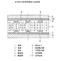
ここで、図1を参照して本発明における課題を解決するための手段を説明する。
なお、図1は本発明のマルチドメイン型液晶表示装置の概略的要部断面図である。
図1参照
(1)本発明は、互いに対向する二枚の基板1,2の間に誘電率異方性が正の液晶3を挟持するとともに、両方の基板1,2の対向する表面に絶縁性の突起状の構造物4,5を1画素内に複数設け、垂直配向膜7,8を構造物4,5の表面に沿って基板1,2の全面を覆うように設けて電圧無印加時における液晶分子6の配向を基板1,2の厚さ方向に歪ませるとともに、電圧を二枚の基板1,2の間に印加するマルチドメイン型液晶表示装置において、電圧無印加時における液晶分子6の配向が二枚の基板1,2の間の中心面に対して対称になっていることを特徴とする。
【0013】
この様に、液晶分子6の配向を二枚の基板1,2の間の中心面に対して対称にすることにより、絶縁性の突起状の構造物4,5の近傍に局在している液晶分子6のみが、構造物4,5の傾斜によってベント配向して表示に寄与するため、液晶配向する時間が短くなり、応答速度が向上する。
なお、この様に、液晶分子6の配向を二枚の基板1,2の間の中心面に対して対称にするためには、両方の構造物4,5が互いに投影的に重なるように対称に設ければ良い。
【0014】
(2)また、本発明は、互いに対向する二枚の基板1,2の間に誘電率異方性が正の液晶3を挟持するとともに、一方の基板1の他方の基板2に対向する表面に絶縁性の突起状の構造物4を1画素内に複数設け、垂直配向膜7を前記構造物4の表面に沿って前記基板1の全面を覆うように設けて電圧無印加時における液晶分子6の配向を前記基板1,2の厚さ方向に歪ませるとともに、電圧を前記二枚の基板1,2の間に印加するマルチドメイン型液晶表示装置において、電圧無印加時における液晶分子6の配向が構造物4の基板1に垂直な中心線に対して対称になっていることを特徴とする。
【0015】
この様に、絶縁性の突起状の構造物4を一方の基板1にのみ設けた場合にも、構造物4の近傍に局在している液晶分子6のみが、構造物4の傾斜によってHAN(Hybrid Aligned Nematic)型に配向して表示に寄与するため、液晶配向する時間が短くなり、応答速度が向上する。
【0017】
特に、垂直配向膜7,8と正の誘電率異方性を有する液晶3を組み合わせて用いることによって、構造物4,5の近傍に局在する液晶分子6のみを表示に寄与させることができ、確実に応答時間を速くすることができる。
即ち、正の誘電率異方性を有する液晶3を用いているので、構造物4,5から離れた領域における液晶分子6は、電圧の印加状態の如何に拘わらず、常に垂直配向しているので表示は寄与しないことになる。
【0018】
また、本発明は、上記(1)乃至(3)のいずれかにおいて、構造物4,5が、基板1,2の厚さ方向の断面形状が半円形状、矩形状、台形状、或いは、三角形状のいずれかの形状の突起であることが望ましい。
【0019】
この様に、構造物4,5としては、構造物4,5の近傍に局在する液晶分子6が十分傾斜して配向するように、基板1,2の厚さ方向の断面形状が半円形状、矩形状、台形状、或いは、三角形状のいずれかの形状の突起であることが望ましい。
【0024】
【発明の実施の形態】
ここで、図2を参照して本発明の第1の実施の形態のマルチドメイン型液晶表示装置を説明する。
なお、図においては、TFT基板、CF基板、TFT等のアクティブ素子、及び、偏光板等の図示を省略している。
図2(a)参照
図2(a)は、本発明の第1の実施の形態のマルチドメイン型液晶表示装置の概略的要部断面図であり、中央の一点鎖線より左側は電圧を印加しない状態を示し、右側は電圧を印加した状態を示している。
図に示すように、ITOからなるTFT基板側透明電極11及びCF基板側透明電極21上に、透明度の高いフォトレジスト、例えば、ポジ型フォトレジストPC−335(JSR製商品名)を塗布してパターニングすることによって、例えば、幅が5μmで高さが5μmの半円状の突起12,22を形成し、全面に垂直配向膜13,23を設ける。
【0025】
図2(b)参照
図2(b)は、突起12の概略的パターンを示す平面図であり、画素マトリクス16に対して突起12は山折れ状のパターンとなっており、隣接する突起12の間隔、即ち、突起12の中心線の間隔は、例えば、13μmにする。
なお、図示を省略するものの、突起22も全く同様のパターンに形成する。
【0026】
再び、図2(a)参照
次いで、TFT基板側透明電極11とCF基板側透明電極21とを突起12と突起22とが投影的に重なるように対向させ、スペーサ(図示せず)を用いてTFT基板側透明電極11とCF基板側透明電極21との間に正の誘電率異方性を有する液晶14を注入して液晶セルを構成する。
なお、互いに対向する突起12と突起22との間隔、即ち、セルギャップは10μmとする。
【0027】
この場合、液晶14を構成する液晶分子15は、垂直配向膜13,23の法線方向に沿って垂直配向することになるが、突起12,22の近傍においては、突起12,22を覆う垂直配向膜13,23の表面の法線方向が基板の厚さ方向に対して傾斜するので、液晶分子15が傾斜してベント配向となる。
【0028】
したがって、偏光板(図示を省略)を図9(a)に示すようにクロスニコルにした場合には、電圧無印加時には、突起12,22の近傍の液晶分子15の配向が表示に寄与して“白”表示となる。
【0029】
一方、電圧印加時においては、突起12,22の近傍の液晶分子15も、正の誘電率異方性によって電圧印加方向に沿って垂直配向するので、“黒”表示となる。
なお、突起12,22から離れた領域における液晶分子15は、電圧の印加状態の如何によらず常に垂直配向しているので、表示に寄与することはない。
【0030】
この様に、本発明の第1の実施の形態においては、表示に寄与するのは突起12,22の近傍に局在する液晶分子15のみであるので、液晶配向が伝播する時間が短くなり、且つ、突起12,22の近傍における液晶分子15のベンド配向によってOCB(光学補償ベンド配向)効果(必要ならば、例えば、S.Onda et al.,Asia Display ‘98 Digest,p.1055,1988参照)が得られるので、応答速度が短くなる。
なお、この場合、突起12,22から離れた領域の液晶が表示に寄与しないので、輝度が低くなるが、隣接する突起12,22同士の間隔を狭めることで輝度の低下を抑制することができる。
但し、あまり間隔を狭くすると液晶分子15の配向が乱れる問題がある。
【0031】
次に、図3を参照して、本発明の第1の実施の形態の変形例を二つ説明するが、突起の形状が異なるだけで、製造工程及び使用材料は第1の実施の形態と全く同様であるので、工程等の説明は省略する。
図3(a)参照
図3(a)は、本発明の第1の実施の形態の変形例の概略的要部断面図であり、この場合の突起17,24は、例えば、幅3μmで高さが3μmの矩形状であり、また、突起17,24の中心線の間隔は8μmとし、且つ、互いに対向する突起17と突起24との間隔、即ち、セルギャップは8μmとする。
【0032】
この変形例においては、突起17,24の形状が矩形状であるので、液晶分子15のベンド配向が非常に強くなり、それによって、パネルの透過率が高くなるので明るい表示が可能になる。
但し、この様な矩形状の突起17,24を設けた場合に、垂直配向膜13,23を均一に塗布することが困難になる。
【0033】
図3(b)参照
図3(b)は、本発明の第1の実施の形態の他の変形例の概略的要部断面図であり、この場合の突起18,25は、例えば、幅5μmで高さが5μmの三角形状であり、また、突起18,25の中心線の間隔は13μmとし、且つ、互いに対向する突起18と突起25との間隔、即ち、セルギャップは10μmとする。
【0034】
この変形例においては、突起18,25の形状が三角形状であるので、液晶分子15のベンド配向が第1の実施の形態より強くなり、パネルの透過率が高くなるので明るい表示が可能になる。
【0035】
次に、図4を参照して、本発明の第2の実施の形態を説明するが、基本的構成は上記第1の実施の形態と同様である。
図4参照
図4は、本発明の第2の実施の形態のマルチドメイン型液晶表示装置の概略的要部断面図であり、中央の一点鎖線より左側は電圧を印加しない状態を示し、右側は電圧を印加した状態を示している。
図に示すように、ITOからなるTFT基板側透明電極11及びCF基板側透明電極21上に、透明度の高いフォトレジスト、例えば、ポジ型フォトレジストPC−335(JSR製商品名)を塗布してパターニングすることによって、図3(b)に示す実施例と同様に、例えば、幅が5μmで高さが5μmの三角形状の突起18,25を形成し、次いで、全面に水平配向膜19,26を設ける。
なお、この場合も、隣接する突起18,25の間隔、即ち、突起18,25の中心線の間隔は、例えば、13μmにする。
【0036】
次いで、TFT基板側透明電極11とCF基板側透明電極21とを突起18と突起25とが投影的に重なるように対向させ、スペーサ(図示せず)を用いてTFT基板側透明電極11とCF基板側透明電極21との間に正の誘電率異方性を有する液晶14を注入して液晶セルを構成する。
なお、互いに対向する突起18と突起25との間隔、即ち、セルギャップは10μmとする。
【0037】
この場合、液晶14を構成する液晶分子15は、突起18,25の近傍においては、突起18,25を覆う水平配向膜19,26の表面の形状に沿って傾斜するので、液晶分子15は上記の図3(b)の場合とは逆に傾斜するベント配向となる。
【0038】
したがって、この場合にも、偏光板(図示を省略)をクロスニコルにした場合には、電圧無印加時には、突起18,25の近傍の液晶分子15の配向が表示に寄与して“白”表示となる。
一方、電圧印加時においては、突起18,25の近傍の液晶分子15も、正の誘電率異方性によって電圧印加方向に沿って垂直配向するので、“黒”表示となる。
【0039】
この様に、本発明の第2の実施の形態においても、表示に実効的に寄与するのは突起18,25の近傍に局在する液晶分子15のみであるので、液晶配向が伝播する時間が短くなり、応答速度が短くなる。
【0040】
次に、図5を参照して本発明の第3の実施の形態のマルチドメイン型液晶表示装置を説明するが、この第3の実施の形態においては、一方の基板側にのみ突起を設けただけで、他の構成は上記の第1の実施の形態と同様である。
なお、この場合も、TFT基板、CF基板、TFT等のアクティブ素子、及び、偏光板等の図示を省略している。
図5参照
図5は、本発明の第3の実施の形態のマルチドメイン型液晶表示装置の概略的要部断面図であり、中央の一点鎖線より左側は電圧を印加しない状態を示し、右側は電圧を印加した状態を示している。
図に示すように、ITOからなるTFT基板側透明電極11上に、透明度の高いフォトレジスト、例えば、ポジ型フォトレジストPC−335(JSR製商品名)を塗布してパターニングすることによって、例えば、幅が5μmで高さが5μmの半円状の突起12を形成し、次いで、TFT基板側透明電極11及びCF基板側透明電極21の全面に垂直配向膜13,23を設ける。
なお、この場合も隣接する突起12の間隔、即ち、突起12の中心線の間隔は、例えば、13μmにする。
【0041】
次いで、TFT基板側透明電極11とCF基板側透明電極21とを対向させ、スペーサ(図示せず)を用いてTFT基板側透明電極11とCF基板側透明電極21との間に正の誘電率異方性を有する液晶14を注入して液晶セルを構成する。
なお、互いに対向する突起12とCF基板側透明電極21との間隔、即ち、セルギャップは10μmとする。
【0042】
この場合、液晶14を構成する液晶分子15は、垂直配向膜13,23の法線方向に沿って垂直配向することになるが、突起12の近傍においてのみ、突起12を覆う垂直配向膜13の表面の法線方向が基板の厚さ方向に対して傾斜するので、液晶分子15は傾斜してHAN型にハイブリッド配向する。
【0043】
したがって、偏光板(図示を省略)をクロスニコルにした場合には、電圧無印加時には、突起12の近傍の液晶分子15の配向が表示に寄与して“白”表示となる。
一方、電圧印加時においては、突起12の近傍の液晶分子15も、正の誘電率異方性によって電圧印加方向に沿って垂直配向するので、“黒”表示となる。
なお、突起12から離れた領域における液晶分子15は、電圧の印加状態の如何によらず常に垂直配向しているので、表示に寄与することはない。
【0044】
この様に、本発明の第3の実施の形態においては、表示に寄与するのは突起12の近傍に局在する液晶分子15のみであるので、液晶配向が伝播する時間が短くなり、応答速度が短くなる。
【0045】
次に、図6を参照して、本発明の第3の実施の形態の変形例を二つ説明するが、突起の形状が異なるだけで、製造工程及び使用材料は第3の実施の形態と全く同様であるので、工程等の説明は省略する。
図6(a)参照
図6(a)は、本発明の第3の実施の形態の変形例の概略的要部断面図であり、この場合の突起17は、例えば、幅3μmで高さが3μmの矩形状であり、また、突起17の中心線の間隔は8μmとし、且つ、互いに対向する突起17とCF基板側透明電極21との間隔、即ち、セルギャップは5μmとする。
【0046】
この変形例においては、突起17の形状が矩形状であるので、図3(a)の場合と同様に、液晶分子15のHAN型のハイブリッド配向が非常に強くなり、パネルの透過率が高くなるので明るい表示が可能になる。
但し、この様な矩形状の突起17を設けた場合に、垂直配向膜13を均一に塗布することが困難になる。
【0047】
図6(b)参照
図6(b)は、本発明の第3の実施の形態の他の変形例の概略的要部断面図であり、この場合の突起18は、例えば、幅5μmで高さが5μmの三角形状であり、また、突起18の中心線の間隔は13μmとし、且つ、互いに対向する突起18とCF基板側透明電極21との間隔、即ち、セルギャップは8μmとする。
【0048】
この変形例においては、突起18の形状が三角形状であるので、液晶分子15のHAN型のハイブリッド配向が第3の実施の形態より強くなり、パネルの透過率が高くなるので明るい表示が可能になる。
【0049】
次に、図7を参照して、本発明の第4の実施の形態を説明するが、基本的構成は上記第3の実施の形態と同様である。
図7参照
図7は、本発明の第4の実施の形態のマルチドメイン型液晶表示装置の概略的要部断面図であり、中央の一点鎖線より左側は電圧を印加しない状態を示し、右側は電圧を印加した状態を示している。
図に示すように、ITOからなるTFT基板側透明電極11上に、透明度の高いフォトレジスト、例えば、ポジ型フォトレジストPC−335(JSR製商品名)を塗布してパターニングすることによって、図6(b)に示す実施例と同様に、例えば、幅が5μmで高さが5μmの三角形状の突起18を形成し、次いで、全面に水平配向膜19,26を設ける。
【0050】
次いで、TFT基板側透明電極11とCF基板側透明電極21とを対向させ、スペーサ(図示せず)を用いてTFT基板側透明電極11とCF基板側透明電極21との間に正の誘電率異方性を有する液晶14を注入して液晶セルを構成する。
なお、互いに対向する突起18とCF基板側透明電極21との間隔、即ち、セルギャップは8μmとする。
【0051】
この場合、液晶14を構成する液晶分子15は、突起18の近傍においては、突起18を覆う水平配向膜19の表面の形状に沿って傾斜するので、液晶分子15はHAN型のハイブリッド配向となる。
【0052】
したがって、この場合にも、偏光板(図示を省略)をクロスニコルにした場合には、電圧無印加時には、突起18の近傍の液晶分子15の配向が表示に寄与して“白”表示となる。
一方、電圧印加時においては、突起18の近傍の液晶分子15も、正の誘電率異方性によって電圧印加方向に沿って垂直配向するので、“黒”表示となる。
【0053】
この様に、本発明の第4の実施の形態においても、表示に実効的に寄与するのは突起18の近傍に局在する液晶分子15のみであるので、液晶配向が伝播する時間が短くなり、応答速度が短くなる。
【0054】
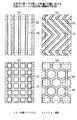
次に、図8を参照して、本発明の第1乃至第4の実施の形態における突起のパターンの変形例を4つ説明するが、各図は突起のパターンを示す概略的平面図である。
図8(a)参照
図8(a)の場合には、突起31をデータバスライン或いはゲートバスラインに沿って直線状の突起にしたものであり、最も簡単なパターンとしている。
【0055】
図8(b)参照
図8(b)の場合には、突起32を山折れ状の波型にしたものであり、実質的には、図2(b)に示したパターンと同様であり、図8(a)の場合に比べて液晶分子の配向方向が紙面の上下方向に分散するので視野角が広くなる利点がある。
【0056】
図8(c)参照
図8(c)の場合には、突起33を格子状にしたものであり、この場合も液晶分子の配向方向が紙面の上下方向に分散するので図8(a)の場合に比べて視野角を広くすることができる。
【0057】
図8(d)参照
図8(d)の場合には、突起34をハニカム状にしたものであり、この場合も液晶分子の配向方向が紙面の上下方向に分散するので図8(a)の場合に比べて視野角を広くすることができる。
【0072】
以上、本発明の各実施の形態を説明してきたが、本発明は各実施の形態に記載した構成及び条件に限られるものではなく、各種の変更が可能である。
例えば、上記の第1乃至第4の実施の形態においては、液晶として、正の誘電率異方性を有する液晶を用いているが、従来のMVA型液晶表示装置と同様に負の誘電率異方性を有する液晶を用いても良いものであり、その場合には、電圧印加とともにベンド配向或いはHAN型配向が強くなるので、上記の第1乃至第4の実施の形態とは逆に“黒”表示となる。
【0073】
また、上記の第1乃至第4の実施の形態においては、偏光板をクロスニコル配置にして、ノーマリホワイト表示にしているが、偏光板をパラニコル配置にしてノーマリブラック表示にしても良いものである。
【0074】
また、上記の第3及び第4の実施の形態においては、突起をTFT基板側に設けているが、逆にCF基板側に設けても良いものであり、第3及び第4の実施の形態と全く同様な効果が得られるものである。
【0080】
【発明の効果】
本発明によれば、基板の少なくとも一方に設けた突起の近傍に局在する液晶分子のみの配向に対する寄与を利用しているので、低階調を含めた全階調において応答速度を改善することができ、それによって、広視野角のMVA型液晶表示装置の高速化に寄与するところが大きい。
【図面の簡単な説明】
【図1】本発明の原理的構成の説明図である。
【図2】本発明の第1の実施の形態の概略的要部構造図である。
【図3】本発明の第1の実施の形態の変形例の概略的要部断面図である。
【図4】本発明の第2の実施の形態の概略的要部断面図である。
【図5】本発明の第3の実施の形態の概略的要部断面図である。
【図6】本発明の第3の実施の形態の変形例の概略的要部断面図である。
【図7】本発明の第4の実施の形態の概略的要部断面図である。
【図8】本発明の第1乃至第4の実施の形態における突起のパターンの変形例の概略的平面図である。
【図9】 従来のMVA型液晶表示装置の説明図である。
【図10】 従来のMVA型液晶表示装置の特性の説明図である。
【符号の説明】
1 基板
2 基板
3 液晶
4 構造物
5 構造物
6 液晶分子
7 垂直配向膜
8 垂直配向膜
9 透明電極
10 透明電極
11 TFT基板側透明電極
12 突起
13 垂直配向膜
14 液晶
15 液晶分子
16 画素マトリクス
17 突起
18 突起
19 水平配向膜
21 CF基板側透明電極
22 突起
23 垂直配向膜
24 突起
25 突起
26 水平配向膜
31 突起
32 突起
33 突起
34 突起
61 TFT基板
62 画素電極
63 突起
64 垂直配向膜
65 CF基板
66 共通電極
67 突起
68 垂直配向膜
69 液晶
70 液晶分子
71 偏光板
72 偏光板[0001]
BACKGROUND OF THE INVENTION
The present invention relates to a multi-domain liquid crystal display device, and more particularly to a multi-domain liquid crystal display device characterized by a structure for improving response speed in a high-quality MVA (multi-domain vertical alignment) liquid crystal display device. Is.
[0002]
[Prior art]
In recent years, with the widespread use of information equipment, there has been a demand for higher performance display panels. To meet these demands, a negative alignment liquid crystal that uses a vertical alignment film and has negative dielectric anisotropy is combined. Further, an MVA liquid crystal display device (Japanese Patent Laid-Open No. 11-242225, if necessary) in which liquid crystal molecules are aligned in a plurality of directions is attracting attention.
[0003]
Here, explaining the conventional MVA type liquid crystal display device with reference to FIG.
Figure 9 (a) see FIG. 9 (a) is a schematic fragmentary sectional view of a conventional MVA type liquid crystal display device in a state where no voltage is applied, the
On the other hand, on the CF (color filter)
[0004]
In this case, the
On the other hand, the
[0005]
In such a liquid crystal display device, the polarizing
[0006]
See FIG. 9 (b) diagram. 9 (b) is a diagram showing the arrangement of the
[0007]
As described above, in the MVA liquid crystal display device, since the
[0008]
[Problems to be solved by the invention]
However, even in such an MVA type liquid crystal display device, it takes time for the tilt of the liquid crystal alignment to propagate through the structure that regulates the tilt direction, that is, the region without the
In particular, when the halftone display has a low gradation, there is a problem in that the propagation of the liquid crystal alignment is slow because the voltage is low, and the response time is three times or more the normal time.
[0009]
Figure 10 Referring to FIG. 10 is an explanatory view of an example of a characteristic of the conventional MVA type liquid crystal display device, ● is a characteristic curve showing an applied voltage dependence of the transmittance, ■ the applied voltage dependence of the response speed It is the characteristic curve shown.
As is apparent from the figure, the transmittance increases as the applied voltage increases, whereas the response speed increases as the applied voltage increases, but tends to decrease again at about 4.5V.
[0010]
Therefore, in the case of low gradation halftone display, since the applied voltage is low, the response speed is 100 ms or more, and there is a problem that a display in which an image flows can be seen when displaying a moving image.
[0011]
Therefore, an object of the present invention is to improve response speed without impairing display quality.
[0012]
[Means for Solving the Problems]
Here, means for solving the problems in the present invention will be described with reference to FIG.
FIG. 1 is a schematic cross-sectional view of the main part of the multi-domain liquid crystal display device of the present invention.
See FIG. 1. (1) The present invention sandwiches a
[0013]
In this way, the orientation of the
In this way, in order to make the orientation of the
[0014]
(2) Further, according to the present invention, the
[0015]
In this way, even when the insulating protrusion-
[0017]
In particular, by using the
That is, since the
[0018]
Further, according to the present invention, in any one of the above (1) to (3), the
[0019]
As described above, the
[0024]
DETAILED DESCRIPTION OF THE INVENTION
Here, the multi-domain liquid crystal display device according to the first embodiment of the present invention will be described with reference to FIG.
In the figure, illustration of active elements such as a TFT substrate, a CF substrate, a TFT, a polarizing plate, and the like is omitted.
FIG. 2A is a schematic cross-sectional view of the main part of the multi-domain type liquid crystal display device according to the first embodiment of the present invention, and no voltage is applied to the left side of the central one-dot chain line. The right side shows a state in which a voltage is applied.
As shown in the figure, on the TFT substrate side
[0025]
FIG. 2B is a plan view showing a schematic pattern of the
Although not shown, the
[0026]
Again referring to FIG. 2A, the TFT substrate side
The interval between the
[0027]
In this case, the
[0028]
Therefore, when the polarizing plate (not shown) in a cross nicol state, as shown in FIG. 9 (a), when no voltage is applied, and contribute to the display orientation of the
[0029]
On the other hand, when a voltage is applied, the
Note that the
[0030]
As described above, in the first embodiment of the present invention, only the
In this case, since the liquid crystal in the region away from the
However, if the interval is too narrow, there is a problem that the alignment of the
[0031]
Next, with reference to FIG. 3, two modified examples of the first embodiment of the present invention will be described. However, the manufacturing process and the materials used are different from those of the first embodiment except that the shape of the protrusions is different. Since it is completely the same, description of a process etc. is abbreviate | omitted.
FIG. 3A is a schematic cross-sectional view of an essential part of a modification of the first embodiment of the present invention. In this case, the
[0032]
In this modified example, since the
However, when such
[0033]
FIG. 3B is a schematic cross-sectional view of an essential part of another modification of the first embodiment of the present invention. In this case, the
[0034]
In this modification, since the
[0035]
Next, a second embodiment of the present invention will be described with reference to FIG. 4, but the basic configuration is the same as that of the first embodiment.
FIG. 4 is a schematic cross-sectional view of the main part of the multi-domain liquid crystal display device according to the second embodiment of the present invention. The left side of the central one-dot chain line shows a state in which no voltage is applied, and the right side A state in which a voltage is applied is shown.
As shown in the figure, on the TFT substrate side
Also in this case, the interval between the
[0036]
Next, the TFT substrate side
The interval between the
[0037]
In this case, the
[0038]
Therefore, also in this case, when the polarizing plate (not shown) is crossed Nicol, when no voltage is applied, the orientation of the
On the other hand, when a voltage is applied, the
[0039]
As described above, also in the second embodiment of the present invention, only the
[0040]
Next, a multi-domain liquid crystal display device according to a third embodiment of the present invention will be described with reference to FIG. 5. In this third embodiment, a protrusion is provided only on one substrate side. However, other configurations are the same as those of the first embodiment.
Also in this case, illustration of active elements such as TFT substrates, CF substrates, TFTs, polarizing plates, and the like is omitted.
FIG. 5 is a schematic cross-sectional view of a main part of a multi-domain liquid crystal display device according to a third embodiment of the present invention. The left side of the central one-dot chain line shows a state in which no voltage is applied, and the right side A state in which a voltage is applied is shown.
As shown in the figure, on the TFT substrate side
Also in this case, the interval between the
[0041]
Next, the TFT substrate side
In addition, the space | interval of the processus |
[0042]
In this case, the
[0043]
Therefore, when the polarizing plate (not shown) is crossed Nicol, when no voltage is applied, the orientation of the
On the other hand, when a voltage is applied, the
Note that the
[0044]
As described above, in the third embodiment of the present invention, only the
[0045]
Next, two modified examples of the third embodiment of the present invention will be described with reference to FIG. 6. However, the manufacturing process and the materials used are different from those of the third embodiment except that the shape of the protrusions is different. Since it is completely the same, description of a process etc. is abbreviate | omitted.
FIG. 6A is a schematic cross-sectional view of a principal part of a modification of the third embodiment of the present invention. In this case, the
[0046]
In this modified example, since the shape of the
However, when such a
[0047]
FIG. 6B is a schematic cross-sectional view of the main part of another modification of the third embodiment of the present invention. In this case, the
[0048]
In this modification, since the shape of the
[0049]
Next, a fourth embodiment of the present invention will be described with reference to FIG. 7, but the basic configuration is the same as that of the third embodiment.
FIG. 7 is a schematic cross-sectional view of a main part of a multi-domain liquid crystal display device according to a fourth embodiment of the present invention. The left side of the central one-dot chain line shows a state in which no voltage is applied, and the right side A state in which a voltage is applied is shown.
As shown in the figure, a highly transparent photoresist, for example, positive photoresist PC-335 (trade name of JSR) is applied and patterned on the TFT substrate-side
[0050]
Next, the TFT substrate side
In addition, the space | interval of the
[0051]
In this case, the
[0052]
Therefore, also in this case, when the polarizing plate (not shown) is crossed Nicol, when no voltage is applied, the orientation of the
On the other hand, when a voltage is applied, the
[0053]
As described above, also in the fourth embodiment of the present invention, only the
[0054]
Next, with reference to FIG. 8, four modified examples of the pattern of protrusions in the first to fourth embodiments of the present invention will be described. Each figure is a schematic plan view showing the pattern of protrusions. .
Reference to FIG. 8A In the case of FIG. 8A, the
[0055]
In the case of FIG. 8B, the
[0056]
Reference to FIG. 8C In the case of FIG. 8C, the
[0057]
In the case of FIG. 8D, the
[0072]
Although the embodiments of the present invention have been described above, the present invention is not limited to the configurations and conditions described in the embodiments, and various modifications can be made.
For example, in the above first to fourth embodiments, a liquid crystal having positive dielectric anisotropy is used as the liquid crystal, but the negative dielectric constant is different from that of the conventional MVA liquid crystal display device. In this case, bend alignment or HAN type alignment becomes stronger as voltage is applied. In contrast to the first to fourth embodiments described above, “black” is used. "Is displayed.
[0073]
In the first to fourth embodiments described above, the polarizing plates are arranged in a crossed Nicols arrangement for normally white display. However, the polarizing plates may be arranged in a paranicols arrangement for normally black display. It is.
[0074]
In the third and fourth embodiments described above, the protrusion is provided on the TFT substrate side, but conversely, it may be provided on the CF substrate side, and the third and fourth embodiments. The same effect can be obtained.
[0080]
【The invention's effect】
According to the present invention, to improve the response speed in all gradations, including utilizing a contribution Tei Runode, the low tone with respect to the orientation of the liquid crystal molecules only localized in the vicinity of the projection provided on at least one of the substrates As a result, it greatly contributes to speeding up the MVA liquid crystal display device with a wide viewing angle.
[Brief description of the drawings]
FIG. 1 is an explanatory diagram of a basic configuration of the present invention.
FIG. 2 is a schematic structural diagram of an essential part of the first embodiment of the present invention.
FIG. 3 is a schematic cross-sectional view of an essential part of a modification of the first embodiment of the present invention.
FIG. 4 is a schematic cross-sectional view of a main part of a second embodiment of the present invention.
FIG. 5 is a schematic cross-sectional view of an essential part of a third embodiment of the present invention.
FIG. 6 is a schematic cross-sectional view of an essential part of a modification of the third embodiment of the present invention.
FIG. 7 is a schematic cross-sectional view of a main part of a fourth embodiment of the present invention.
FIG. 8 is a schematic plan view of a modification of the pattern of protrusions in the first to fourth embodiments of the present invention.
FIG. 9 is an explanatory diagram of a conventional MVA liquid crystal display device.
FIG. 10 is an explanatory diagram of characteristics of a conventional MVA liquid crystal display device.
[Explanation of symbols]
DESCRIPTION OF
61
Claims (2)
Priority Applications (1)
| Application Number | Priority Date | Filing Date | Title |
|---|---|---|---|
| JP2000045403A JP4606540B2 (en) | 2000-02-23 | 2000-02-23 | Multi-domain liquid crystal display device |
Applications Claiming Priority (1)
| Application Number | Priority Date | Filing Date | Title |
|---|---|---|---|
| JP2000045403A JP4606540B2 (en) | 2000-02-23 | 2000-02-23 | Multi-domain liquid crystal display device |
Publications (2)
| Publication Number | Publication Date |
|---|---|
| JP2001235748A JP2001235748A (en) | 2001-08-31 |
| JP4606540B2 true JP4606540B2 (en) | 2011-01-05 |
Family
ID=18567995
Family Applications (1)
| Application Number | Title | Priority Date | Filing Date |
|---|---|---|---|
| JP2000045403A Expired - Fee Related JP4606540B2 (en) | 2000-02-23 | 2000-02-23 | Multi-domain liquid crystal display device |
Country Status (1)
| Country | Link |
|---|---|
| JP (1) | JP4606540B2 (en) |
Families Citing this family (13)
| Publication number | Priority date | Publication date | Assignee | Title |
|---|---|---|---|---|
| JP3338025B2 (en) * | 1999-10-05 | 2002-10-28 | 松下電器産業株式会社 | Liquid crystal display device |
| JP4248835B2 (en) | 2002-04-15 | 2009-04-02 | シャープ株式会社 | Substrate for liquid crystal display device and liquid crystal display device including the same |
| JP4248306B2 (en) | 2002-06-17 | 2009-04-02 | シャープ株式会社 | Liquid crystal display |
| KR100945372B1 (en) | 2002-12-31 | 2010-03-08 | 엘지디스플레이 주식회사 | Multi-domain liquid crystal display device |
| JP2005215115A (en) * | 2004-01-28 | 2005-08-11 | Fujitsu Display Technologies Corp | Liquid crystal display device |
| JP2006091547A (en) | 2004-09-24 | 2006-04-06 | Sharp Corp | Liquid crystal panel and liquid crystal display device |
| JP4648169B2 (en) * | 2005-11-25 | 2011-03-09 | 株式会社 日立ディスプレイズ | Liquid crystal display device |
| JP5436844B2 (en) * | 2008-12-03 | 2014-03-05 | スタンレー電気株式会社 | Character type vertical alignment liquid crystal display device |
| US20100134749A1 (en) | 2008-12-03 | 2010-06-03 | Stanley Electric Co., Ltd. | Character type vertical alignment mode liquid crystal display device with wall layers |
| JP5281376B2 (en) * | 2008-12-04 | 2013-09-04 | スタンレー電気株式会社 | Character type vertical alignment liquid crystal display device |
| JP5617256B2 (en) * | 2010-01-27 | 2014-11-05 | 株式会社ニコン | Liquid crystal display device manufacturing method and exposure apparatus |
| JP2011197493A (en) * | 2010-03-23 | 2011-10-06 | Stanley Electric Co Ltd | Vertical alignment liquid crystal display element |
| JP2020129081A (en) * | 2019-02-08 | 2020-08-27 | 株式会社ジャパンディスプレイ | Laser scanner and distance measuring device |
Citations (8)
| Publication number | Priority date | Publication date | Assignee | Title |
|---|---|---|---|---|
| JPH07311383A (en) * | 1994-05-18 | 1995-11-28 | Sanyo Electric Co Ltd | Liquid crystal display device |
| JPH1172793A (en) * | 1997-08-29 | 1999-03-16 | Sharp Corp | Liquid crystal display device and its production |
| JPH11101993A (en) * | 1997-08-01 | 1999-04-13 | Canon Inc | Liquid crystal element, method for controlling orientation of liquid crystal and manufacture of liquid crystal element |
| JPH11242225A (en) * | 1997-06-12 | 1999-09-07 | Fujitsu Ltd | Liquid crystal display device |
| JPH11295739A (en) * | 1998-04-15 | 1999-10-29 | Nec Corp | Liquid crystal display device, manufacture and driving method thereof |
| JPH11352491A (en) * | 1998-05-20 | 1999-12-24 | Samsung Electronics Co Ltd | Wide visual field angle liquid crystal display device |
| JPH11352487A (en) * | 1998-06-10 | 1999-12-24 | Canon Inc | Liquid crystal element and its drive method |
| JPH11352483A (en) * | 1998-05-29 | 1999-12-24 | Hyundai Electronics Ind Co Ltd | Perpendicularly aligned liquid crystal display device having multiple domains |
-
2000
- 2000-02-23 JP JP2000045403A patent/JP4606540B2/en not_active Expired - Fee Related
Patent Citations (8)
| Publication number | Priority date | Publication date | Assignee | Title |
|---|---|---|---|---|
| JPH07311383A (en) * | 1994-05-18 | 1995-11-28 | Sanyo Electric Co Ltd | Liquid crystal display device |
| JPH11242225A (en) * | 1997-06-12 | 1999-09-07 | Fujitsu Ltd | Liquid crystal display device |
| JPH11101993A (en) * | 1997-08-01 | 1999-04-13 | Canon Inc | Liquid crystal element, method for controlling orientation of liquid crystal and manufacture of liquid crystal element |
| JPH1172793A (en) * | 1997-08-29 | 1999-03-16 | Sharp Corp | Liquid crystal display device and its production |
| JPH11295739A (en) * | 1998-04-15 | 1999-10-29 | Nec Corp | Liquid crystal display device, manufacture and driving method thereof |
| JPH11352491A (en) * | 1998-05-20 | 1999-12-24 | Samsung Electronics Co Ltd | Wide visual field angle liquid crystal display device |
| JPH11352483A (en) * | 1998-05-29 | 1999-12-24 | Hyundai Electronics Ind Co Ltd | Perpendicularly aligned liquid crystal display device having multiple domains |
| JPH11352487A (en) * | 1998-06-10 | 1999-12-24 | Canon Inc | Liquid crystal element and its drive method |
Also Published As
| Publication number | Publication date |
|---|---|
| JP2001235748A (en) | 2001-08-31 |
Similar Documents
| Publication | Publication Date | Title |
|---|---|---|
| JP3826217B2 (en) | Fringe field switching mode liquid crystal display | |
| US7586573B2 (en) | Substrate for liquid crystal display and liquid crystal display having the same | |
| JP3926056B2 (en) | Liquid crystal display | |
| US6501524B1 (en) | Liquid crystal display device | |
| JPH1124068A (en) | Method for forming dual domain inside liquid crystal layer, manufacture of liquid crystal display device using the method and liquid crystal display device | |
| JP2001324718A (en) | Structure of multidomain wide viewing angle liquid crystal display | |
| JPH0728063A (en) | Liquid crystal display device | |
| JP4606540B2 (en) | Multi-domain liquid crystal display device | |
| JP4902345B2 (en) | Liquid crystal display element | |
| JP3031317B2 (en) | Active matrix liquid crystal display | |
| KR100833955B1 (en) | Array substate for In Plane Switching mode Liquid crystal display device | |
| KR100688265B1 (en) | Liquid crystal display | |
| US6469764B1 (en) | Liquid crystal display and method for manufacturing the same | |
| JP3684398B2 (en) | Optically compensated splay mode liquid crystal display | |
| JPH07225389A (en) | Liquid crystal display element and its manufacture | |
| JP4447484B2 (en) | Liquid crystal display | |
| WO2020088383A1 (en) | Display substrate, method for manufacturing same, and display device | |
| US20100097559A1 (en) | Simple matrix vertical alignment mode liquid crystal display device with linear wall layers | |
| JP3746333B2 (en) | Liquid crystal display | |
| JP3356273B2 (en) | Liquid crystal display | |
| JPH0713166A (en) | Liquid crystal display element | |
| JP4262001B2 (en) | Vertical alignment mode liquid crystal display device | |
| KR19980077802A (en) | LCD and its manufacturing method | |
| JP4019906B2 (en) | Liquid crystal display | |
| US20040125276A1 (en) | Liquid crystal display |
Legal Events
| Date | Code | Title | Description |
|---|---|---|---|
| A711 | Notification of change in applicant |
Free format text: JAPANESE INTERMEDIATE CODE: A711 Effective date: 20050712 |
|
| A711 | Notification of change in applicant |
Free format text: JAPANESE INTERMEDIATE CODE: A711 Effective date: 20050713 |
|
| RD03 | Notification of appointment of power of attorney |
Free format text: JAPANESE INTERMEDIATE CODE: A7423 Effective date: 20050809 |
|
| A621 | Written request for application examination |
Free format text: JAPANESE INTERMEDIATE CODE: A621 Effective date: 20060810 |
|
| A977 | Report on retrieval |
Free format text: JAPANESE INTERMEDIATE CODE: A971007 Effective date: 20090611 |
|
| A131 | Notification of reasons for refusal |
Free format text: JAPANESE INTERMEDIATE CODE: A131 Effective date: 20090616 |
|
| A521 | Written amendment |
Free format text: JAPANESE INTERMEDIATE CODE: A523 Effective date: 20090806 |
|
| A131 | Notification of reasons for refusal |
Free format text: JAPANESE INTERMEDIATE CODE: A131 Effective date: 20100713 |
|
| A521 | Written amendment |
Free format text: JAPANESE INTERMEDIATE CODE: A523 Effective date: 20100910 |
|
| TRDD | Decision of grant or rejection written | ||
| A01 | Written decision to grant a patent or to grant a registration (utility model) |
Free format text: JAPANESE INTERMEDIATE CODE: A01 Effective date: 20101005 |
|
| A01 | Written decision to grant a patent or to grant a registration (utility model) |
Free format text: JAPANESE INTERMEDIATE CODE: A01 |
|
| A61 | First payment of annual fees (during grant procedure) |
Free format text: JAPANESE INTERMEDIATE CODE: A61 Effective date: 20101006 |
|
| R150 | Certificate of patent or registration of utility model |
Ref document number: 4606540 Country of ref document: JP Free format text: JAPANESE INTERMEDIATE CODE: R150 Free format text: JAPANESE INTERMEDIATE CODE: R150 |
|
| FPAY | Renewal fee payment (event date is renewal date of database) |
Free format text: PAYMENT UNTIL: 20131015 Year of fee payment: 3 |
|
| LAPS | Cancellation because of no payment of annual fees |